KR102545297B1 - Layer Structure for the channel line of Field Effect Transistors - Google Patents
Layer Structure for the channel line of Field Effect Transistors Download PDFInfo
- Publication number
- KR102545297B1 KR102545297B1 KR1020210081012A KR20210081012A KR102545297B1 KR 102545297 B1 KR102545297 B1 KR 102545297B1 KR 1020210081012 A KR1020210081012 A KR 1020210081012A KR 20210081012 A KR20210081012 A KR 20210081012A KR 102545297 B1 KR102545297 B1 KR 102545297B1
- Authority
- KR
- South Korea
- Prior art keywords
- silicon
- germanium
- etching
- field effect
- channel
- Prior art date
- Legal status (The legal status is an assumption and is not a legal conclusion. Google has not performed a legal analysis and makes no representation as to the accuracy of the status listed.)
- Active
Links
Images


Classifications
-
- H—ELECTRICITY
- H10—SEMICONDUCTOR DEVICES; ELECTRIC SOLID-STATE DEVICES NOT OTHERWISE PROVIDED FOR
- H10D—INORGANIC ELECTRIC SEMICONDUCTOR DEVICES
- H10D64/00—Electrodes of devices having potential barriers
- H10D64/01—Manufacture or treatment
- H10D64/017—Manufacture or treatment using dummy gates in processes wherein at least parts of the final gates are self-aligned to the dummy gates, i.e. replacement gate processes
-
- H01L29/66545—
-
- H01L29/0673—
-
- H01L29/42392—
-
- H01L29/78696—
-
- H—ELECTRICITY
- H10—SEMICONDUCTOR DEVICES; ELECTRIC SOLID-STATE DEVICES NOT OTHERWISE PROVIDED FOR
- H10D—INORGANIC ELECTRIC SEMICONDUCTOR DEVICES
- H10D30/00—Field-effect transistors [FET]
- H10D30/60—Insulated-gate field-effect transistors [IGFET]
- H10D30/67—Thin-film transistors [TFT]
- H10D30/6729—Thin-film transistors [TFT] characterised by the electrodes
- H10D30/673—Thin-film transistors [TFT] characterised by the electrodes characterised by the shapes, relative sizes or dispositions of the gate electrodes
- H10D30/6735—Thin-film transistors [TFT] characterised by the electrodes characterised by the shapes, relative sizes or dispositions of the gate electrodes having gates fully surrounding the channels, e.g. gate-all-around
-
- H—ELECTRICITY
- H10—SEMICONDUCTOR DEVICES; ELECTRIC SOLID-STATE DEVICES NOT OTHERWISE PROVIDED FOR
- H10D—INORGANIC ELECTRIC SEMICONDUCTOR DEVICES
- H10D30/00—Field-effect transistors [FET]
- H10D30/60—Insulated-gate field-effect transistors [IGFET]
- H10D30/67—Thin-film transistors [TFT]
- H10D30/6757—Thin-film transistors [TFT] characterised by the structure of the channel, e.g. transverse or longitudinal shape or doping profile
-
- H—ELECTRICITY
- H10—SEMICONDUCTOR DEVICES; ELECTRIC SOLID-STATE DEVICES NOT OTHERWISE PROVIDED FOR
- H10D—INORGANIC ELECTRIC SEMICONDUCTOR DEVICES
- H10D62/00—Semiconductor bodies, or regions thereof, of devices having potential barriers
- H10D62/10—Shapes, relative sizes or dispositions of the regions of the semiconductor bodies; Shapes of the semiconductor bodies
- H10D62/117—Shapes of semiconductor bodies
- H10D62/118—Nanostructure semiconductor bodies
- H10D62/119—Nanowire, nanosheet or nanotube semiconductor bodies
- H10D62/121—Nanowire, nanosheet or nanotube semiconductor bodies oriented parallel to substrates
Landscapes
- Insulated Gate Type Field-Effect Transistor (AREA)
Abstract
전계 효과 트랜지스터의 채널 개선 구조 및 그 공정 방법이 제시된다. 본 발명에서 제안하는 전계 효과 트랜지스터의 채널 개선 구조 공정 방법은 실리콘 기판에 채널형성을 위한 이온을 주입하는 단계, 상기 실리콘 기판 상에 실리콘을 에피택셜을 성장시키는 과정에서 열 산화 공정을 통해 중간 절연막이 형성되는 실리콘 층, 상하부 실리콘-게르마늄 희생층 및 상기 실리콘-게르마늄 희생층보다 게르마늄 비율이 더 높은 중간 실리콘-게르마늄 희생층을 번갈아 가며 증착하는 단계, 상기 증착된 실리콘-게르마늄 희생층 상에 더미 게이트를 형성하고, 건식 식각을 통해 소스/드레인 전극 리세스를 형성하는 단계, 상기 실리콘-게르마늄 희생층을 식각 물질을 이용하여 식각하고, 소스/드레인 영역을 에피택셜 증착하는 단계, 실리콘-게르마늄을 식각하고, 절연물질을 증착하여 내부 스페이서를 형성하는 단계 및 채널 부분의 절연물질을 식각하고, 게이트 유전물질 및 게이트 전극을 형성하는 단계를 포함한다.A channel improvement structure of a field effect transistor and a process method thereof are presented. The process method for a channel enhancement structure of a field effect transistor proposed in the present invention includes the steps of implanting ions for channel formation into a silicon substrate, and forming an intermediate insulating film through a thermal oxidation process in the process of epitaxially growing silicon on the silicon substrate. alternately depositing a formed silicon layer, upper and lower silicon-germanium sacrificial layers, and an intermediate silicon-germanium sacrificial layer having a higher germanium ratio than the silicon-germanium sacrificial layer; dummy gates on the deposited silicon-germanium sacrificial layer; and forming source/drain electrode recesses through dry etching, etching the silicon-germanium sacrificial layer using an etching material, epitaxially depositing source/drain regions, etching the silicon-germanium, , depositing an insulating material to form internal spacers, etching the insulating material of the channel portion, and forming a gate dielectric material and a gate electrode.
Description
본 발명은 전계 효과 트랜지스터의 공정과정 중 발생하는 채널의 수직 방향 휨 현상을 개선하는 구조 및 그 공정 방법에 관한 것이다.The present invention relates to a structure and a process method for improving a vertical direction bending phenomenon of a channel generated during a process of manufacturing a field effect transistor.
종래기술에 따른 평면 전계 효과 트랜지스터 구조의 미세화가 한계에 다다르면서, 게이트를 지느러미 모양으로 감싸는 핀형 전계 효과 트랜지스터 구조가 새로운 대안으로 주목받고 있다. 게이트와 채널사이의 접촉면적을 늘린 핀형 전계 효과 트랜지스터 구조가 적용되면서, 누설전류가 감소하고 결과적으로 구동 전압이 낮아지는 효과를 누릴 수 있게 되었다. 그러나 칩의 미세화로 핀형 전계 효과 트랜지스터의 종횡비가 증가하고 그로 인한 공정 비용이 급증하면서 새로운 전계 효과 트랜지스터 구조의 필요성이 제기되었다. As the miniaturization of the planar field effect transistor structure according to the prior art approaches the limit, a fin-type field effect transistor structure that wraps the gate in a fin shape is attracting attention as a new alternative. As the fin-type field effect transistor structure with increased contact area between the gate and the channel is applied, leakage current is reduced and consequently, the effect of lowering the driving voltage can be enjoyed. However, as the aspect ratio of the fin-type field effect transistor increases due to miniaturization of the chip, and process costs accordingly increase, the need for a new field effect transistor structure has been raised.
게이트 올 어라운드(Gate All Around; GAA) 전계 효과 트랜지스터(Field Effect Transistor; FET)는 기존 핀형 전계 효과 트랜지스터(FinFET; Fin Field Effect Transistor) 구조와 달리 채널의 4 면을 모두 게이트가 둘러싸고 있는 구조를 특징으로 한다. 이를 통해 게이트의 전류 조절 능력을 향상시켜, 게이트 누설 전류를 감소시키고 구동 전압을 낮출 수 있다. 또한, 핀형 전계효과 트랜지스터에 비해 작은 종횡비를 가져 공정의 용이성도 향상시킬 수 있었다. 게이트 올 어라운드 나노시트 전계 효과 트랜지스터는 기존 와이어(wire) 모양의 채널을 시트(sheet) 모양으로 확장시킨 구조로서 전류 이동 면적을 크게 증가시킨 구조이다. Gate All Around (GAA) Field Effect Transistor (FET) features a structure in which gates surround all four sides of the channel, unlike the existing fin field effect transistor (FinFET) structure. to be Through this, the current control ability of the gate can be improved, thereby reducing the gate leakage current and lowering the driving voltage. In addition, the ease of processing could be improved by having a smaller aspect ratio than the fin-type field effect transistor. The gate all-around nanosheet field effect transistor is a structure in which a conventional wire-shaped channel is extended into a sheet shape, and the current moving area is greatly increased.
게이트 올 어라운드 나노시트 전계 효과 나노시트 트랜지스터는 공정 과정 중 실리콘 채널이 브릿지 형태로 노출된다. 실리콘 채널이 노출된 상태에서 고온 공정에 노출되면, 재료의 열팽창으로 인해 수직방향으로 휨 현상이 발생하게 되어 소자의 나노구조 정렬의 정확도가 떨어지게 된다.In the gate all-around nanosheet field effect nanosheet transistor, the silicon channel is exposed in the form of a bridge during the process. When exposed to a high-temperature process while the silicon channel is exposed, a bending phenomenon occurs in a vertical direction due to thermal expansion of the material, and thus the accuracy of nanostructure alignment of the device is deteriorated.
본 발명이 이루고자 하는 기술적 과제는 전계 효과 트랜지스터의 고온 공정 시 실리콘 층의 수직방향 휨 현상을 개선하기 위한 전계 효과 트랜지스터의 채널 개선 구조 및 그 공정 방법을 제공하는데 있다. 특히 실리콘 층 사이에 적절한 절연물질을 증착하여 제작 공정 과정 중 실리콘 층이 브릿지 형태로 고온 공정에 노출되는 게이트 올 어라운드 나노시트 전계 효과 트랜지스터의 수직 방향 채널 휨 현상을 개선하고자 한다.A technical problem to be achieved by the present invention is to provide a channel improvement structure of a field effect transistor and a process method for improving a vertical warp phenomenon of a silicon layer during a high-temperature process of a field effect transistor. In particular, an appropriate insulating material is deposited between the silicon layers to improve the vertical channel bending phenomenon of the gate all-around nanosheet field effect transistor in which the silicon layer is exposed to a high-temperature process in the form of a bridge during the fabrication process.
일 측면에 있어서, 본 발명에서 제안하는 전계 효과 트랜지스터의 채널 개선 구조 공정 방법은 실리콘 기판에 채널형성을 위한 이온을 주입하는 단계, 상기 실리콘 기판 상에 실리콘을 에피택셜을 성장시키는 과정에서 열 산화 공정을 통해 중간 절연막이 형성되는 실리콘 층, 상하부 실리콘-게르마늄 희생층 및 상기 실리콘-게르마늄 희생층보다 게르마늄 비율이 더 높은 중간 실리콘-게르마늄 희생층을 번갈아 가며 증착하는 단계, 상기 증착된 실리콘-게르마늄 희생층 상에 더미 게이트를 형성하고, 건식 식각을 통해 소스/드레인 전극 리세스를 형성하는 단계, 상기 실리콘-게르마늄 희생층을 식각 물질을 이용하여 식각하고, 소스/드레인 영역을 에피택셜 증착하는 단계, 실리콘-게르마늄을 식각하고, 절연물질을 증착하여 내부 스페이서를 형성하는 단계 및 채널 부분의 절연물질을 식각하고, 게이트 유전물질 및 게이트 전극을 형성하는 단계를 포함한다. In one aspect, the process method for a channel enhancement structure of a field effect transistor proposed in the present invention includes the steps of implanting ions for channel formation into a silicon substrate, and a thermal oxidation process in the process of epitaxially growing silicon on the silicon substrate. Alternately depositing a silicon layer on which an intermediate insulating film is formed, upper and lower silicon-germanium sacrificial layers, and an intermediate silicon-germanium sacrificial layer having a higher germanium ratio than the silicon-germanium sacrificial layer, the deposited silicon-germanium sacrificial layer Forming a dummy gate on the surface and forming source/drain electrode recesses through dry etching, etching the silicon-germanium sacrificial layer using an etching material, and epitaxially depositing source/drain regions, silicon - Etching germanium and depositing an insulating material to form internal spacers, etching the insulating material of the channel portion, and forming a gate dielectric material and a gate electrode.
상기 실리콘 기판 상에 실리콘을 에피택셜을 성장시키는 과정에서 열 산화 공정을 통해 중간 절연막이 형성되는 실리콘 층, 상하부 실리콘-게르마늄 희생층 및 상기 실리콘-게르마늄 희생층보다 게르마늄 비율이 더 높은 중간 실리콘-게르마늄 희생층을 번갈아 가며 증착하는 단계는 내부 스페이서를 형성하기 위한 실리콘-게르마늄의 식각을 진행할 때, 채널의 위치에 따른 증착 두께의 차이가 발생하여 오버 에칭을 필요로 하지 않도록 수직방향 변위를 일정하게 유지하기 위해 상기 실리콘 층 사이에 중간 절연막을 형성한다. In the process of epitaxially growing silicon on the silicon substrate, a silicon layer in which an intermediate insulating film is formed through a thermal oxidation process, upper and lower silicon-germanium sacrificial layers, and an intermediate silicon-germanium having a higher germanium ratio than the silicon-germanium sacrificial layer In the step of alternately depositing sacrificial layers, when etching silicon-germanium to form internal spacers, a difference in deposition thickness occurs depending on the location of the channel, so that over-etching is not required, so that the vertical displacement is kept constant. In order to do so, an intermediate insulating film is formed between the silicon layers.
본 발명의 일 실시예들에 따른 상기 실리콘 층 사이의 중간 절연막의 절연물질은 실리콘보다 열팽창 계수가 낮은 절연물질을 포함할 수 있다. An insulating material of an intermediate insulating layer between the silicon layers according to an embodiment of the present invention may include an insulating material having a lower coefficient of thermal expansion than silicon.
본 발명의 일 실시예들에 따른 상기 실리콘 층 사이의 중간 절연막의 절연물질은 실리콘 다이옥사이드를 포함하고, 상기 실리콘 층에 대한 상기 중간 절연막의 두께 비율은 전계 효과 트랜지스터의 전기적 특성 및 공정에 따라 조절될 수 있다. According to one embodiment of the present invention, the insulating material of the intermediate insulating film between the silicon layers includes silicon dioxide, and the thickness ratio of the intermediate insulating film to the silicon layer is adjusted according to the electrical characteristics and processes of the field effect transistor. can
본 발명의 일 실시예들에 따른 상기 실리콘 층에 대한 상기 중간 절연막의 두께 비율은 10 ~ 75% 일 수 있다. According to one embodiment of the present invention, a thickness ratio of the intermediate insulating film to the silicon layer may be 10 to 75%.
또 다른 일 측면에 있어서, 본 발명에서 제안하는 전계 효과 트랜지스터의 채널 개선 구조는 채널형성을 위한 이온이 주입된 실리콘 기판, 상기 실리콘 기판 상에 번갈아 가며 증착되는 실리콘 층, 상하부 실리콘-게르마늄 희생층 및 중간 실리콘-게르마늄 희생층을 포함하고, 상기 실리콘 층은 실리콘을 에피택셜 성장시키는 과정에서 열 산화 공정을 통해 중간 절연막이 형성되고, 상기 중간 실리콘-게르마늄 희생층은 상기 상하부 실리콘-게르마늄 희생층보다 게르마늄 비율이 더 높을 수 있다. In another aspect, the channel improvement structure of the field effect transistor proposed in the present invention includes a silicon substrate implanted with ions for channel formation, a silicon layer alternately deposited on the silicon substrate, upper and lower silicon-germanium sacrificial layers, and An intermediate silicon-germanium sacrificial layer is formed on the silicon layer through a thermal oxidation process during epitaxial growth of silicon, and the intermediate silicon-germanium sacrificial layer contains more germanium than the upper and lower silicon-germanium sacrificial layers. ratio could be higher.
본 발명에서 제안하는 전계 효과 트랜지스터의 채널 개선 구조는 상기 증착된 실리콘-게르마늄 희생층 상에 형성되는 더미 게이트, 건식 식각을 통해 소스/드레인 전극 리세스를 형성한 후, 상기 실리콘-게르마늄 희생층을 식각 물질을 이용하여 식각하고, 에피택셜을 통해 증착되는 소스/드레인 영역, 실리콘-게르마늄을 식각하고, 절연물질을 증착하여 형성되는 내부 스페이서 및 채널 부분의 절연물질을 식각하여 형성되는 게이트 유전물질 및 게이트 전극을 더 포함할 수 있다.In the channel improvement structure of the field effect transistor proposed in the present invention, a dummy gate formed on the deposited silicon-germanium sacrificial layer and source/drain electrode recesses are formed through dry etching, and then the silicon-germanium sacrificial layer is formed. A gate dielectric material formed by etching using an etching material, etching the source/drain region and silicon-germanium deposited through epitaxial deposition, and etching the insulating material of the internal spacer and channel portion formed by depositing an insulating material, and A gate electrode may be further included.
본 발명의 실시예들에 따른 전계 효과 트랜지스터의 채널 개선 구조를 통해 전계 효과 트랜지스터의 고온 공정 시 실리콘 층의 수직방향 휨 현상을 개선할 수 있다. 특히 실리콘 층 사이에 적절한 절연물질을 증착하여 제작 공정 과정 중 실리콘 층이 브릿지 형태로 고온 공정에 노출되는 게이트 올 어라운드 나노시트 전계 효과 트랜지스터의 수직 방향 채널 휨 현상을 개선할 수 있다.Through the channel enhancement structure of the field effect transistor according to the embodiments of the present invention, it is possible to improve the vertical direction warpage of the silicon layer during a high-temperature process of the field effect transistor. In particular, by depositing an appropriate insulating material between the silicon layers, it is possible to improve the vertical channel warpage of the gate all-around nanosheet field effect transistor in which the silicon layer is exposed to a high-temperature process in the form of a bridge during the fabrication process.
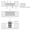
도 1은 종래기술에 따른 게이트 올 어라운드 나노시트 전계 효과 트랜지스터의 전공정 과정을 나태내는 도면이다.
도 2는 본 발명의 일 실시예에 따른 전계효과 트랜지스터의 절연막 증착 공정 중 수직 변위 양상을 설명하기 위한 도면이다.
도 3은 본 발명의 일 실시예에 따른 전계 효과 트랜지스터의 채널 구조 공정 방법을 설명하기 위한 흐름도이다.
도 4는 본 발명의 일 실시예에 따른 전계 효과 트랜지스터의 채널 구조를 나타내는 도면이다.
도 5는 본 발명의 일 실시예에 따른 실리콘 층 내의 중간 절연막의 비율에 따른 수직 변위 양상을 나타내는 도면이다.
도 6은 본 발명의 일 실시예에 따른 실리콘 층 내의 중간 절연막 비율에 따른 수직 변위를 나타내는 그래프이다. 1 is a view showing the entire process of a gate all-around nanosheet field effect transistor according to the prior art.
FIG. 2 is a view for explaining a vertical displacement aspect during a process of depositing an insulating film of a field effect transistor according to an embodiment of the present invention.
3 is a flowchart illustrating a method of processing a channel structure of a field effect transistor according to an embodiment of the present invention.
4 is a diagram showing a channel structure of a field effect transistor according to an embodiment of the present invention.
5 is a view showing a vertical displacement pattern according to a ratio of an intermediate insulating film in a silicon layer according to an embodiment of the present invention.
6 is a graph showing vertical displacement according to a ratio of an intermediate insulating film in a silicon layer according to an embodiment of the present invention.
본 발명은 전계 효과 트랜지스터의 공정과정 중 발생하는 채널의 수직 방향 휨 현상을 개선하는 구조 및 그 공정 방법에 관한 것으로서, 더욱 상세하게는 형성되는 채널에 중간 절연막을 추가하여 수직방향 변위를 개선할 뿐 아니라, 채널의 전기적 특성도 향상시키는 구조 및 그 공정 방법에 관한 것이다. 이하, 본 발명의 실시 예를 첨부된 도면을 참조하여 상세하게 설명한다.The present invention relates to a structure and process method for improving vertical warping of a channel generated during the process of a field effect transistor, and more particularly, by adding an intermediate insulating film to a formed channel to improve vertical displacement. In addition, it relates to a structure and a process method for improving the electrical characteristics of a channel. Hereinafter, embodiments of the present invention will be described in detail with reference to the accompanying drawings.
도 1은 종래기술에 따른 게이트 올 어라운드 나노시트 전계 효과 트랜지스터의 전공정 과정을 나태내는 도면이다. 1 is a view showing the entire process of a gate all-around nanosheet field effect transistor according to the prior art.
종래기술에 따른 게이트 올 어라운드 나노시트 전계 효과 트랜지스터의 전공정 과정은 실리콘 기판에 채널형성을 위한 이온을 주입하는 단계, 상기 실리콘 기판 상에 실리콘 층, 상하부 실리콘-게르마늄 희생층 및 상하부 상기 실리콘-게르마늄 희생층보다 게르마늄 비율이 더 높은 중간 실리콘-게르마늄 희생층을 번갈아 가며 증착하는 단계, 상기 증착된 실리콘-게르마늄 희생층 상에 더미 게이트를 형성하고, 건식 식각을 통해 소스/드레인 전극 리세스를 형성하는 단계, 상기 실리콘-게르마늄 희생층을 식각 물질을 이용하여 식각하고, 소스/드레인 영역을 에피택셜 증착하는 단계, 실리콘-게르마늄을 식각하고, 절연물질을 증착하여 내부 스페이서를 형성하는 단계 및 채널 부분의 절연물질을 식각하고, 게이트 유전물질 및 게이트 전극을 형성하는 단계를 포함한다. The entire process of the gate all-around nanosheet field effect transistor according to the prior art includes implanting ions for channel formation into a silicon substrate, a silicon layer on the silicon substrate, upper and lower silicon-germanium sacrificial layers, and upper and lower silicon-germanium alternately depositing intermediate silicon-germanium sacrificial layers having a higher germanium ratio than the sacrificial layer, forming dummy gates on the deposited silicon-germanium sacrificial layer, and forming source/drain electrode recesses through dry etching; Step, etching the silicon-germanium sacrificial layer using an etching material, epitaxially depositing source/drain regions, etching the silicon-germanium, depositing an insulating material to form internal spacers, and Etching the insulating material and forming a gate dielectric material and a gate electrode.
도 1(a)는 실리콘 기판 상에 채널 절연(Channel Isolation) 이온을 주입하는 과정을 나타내는 도면이다. 1(a) is a diagram illustrating a process of implanting channel isolation ions onto a silicon substrate.
도 1(b)는 실리콘 층(다시 말해, 실리콘 채널(Channel))과 상하부 실리콘-게르마늄 희생층 및 실리콘-게르마늄 희생층보다 게르마늄 비율이 더 높은 중간 실리콘-게르마늄 희생층을 번갈아 가며 증착하는 과정을 나타내는 도면이다. 1(b) shows a process of alternately depositing a silicon layer (ie, a silicon channel), upper and lower silicon-germanium sacrificial layers, and an intermediate silicon-germanium sacrificial layer having a higher germanium ratio than the silicon-germanium sacrificial layer. It is a drawing that represents
도 1(c)는 더미 게이트를 형성하는 과정을 나타내는 도면이고, 도1(d)는 건식 식각을 통해 소스/드레인 전극 리세스를 형성하는 과정을 나타내는 도면이다. FIG. 1(c) is a diagram illustrating a process of forming a dummy gate, and FIG. 1(d) is a diagram illustrating a process of forming source/drain electrode recesses through dry etching.
도 1(e)는 적절한 식각비를 가진 물질을 이용해 실리콘-게르마늄 영역을 식각하는 과정을 나타내는 도면이다. 1(e) is a diagram illustrating a process of etching a silicon-germanium region using a material having an appropriate etching ratio.
도 1(f)는 소스/드레인 영역을 에피택셜 증착하는 과정을 나타내는 도면이다. 1(f) is a diagram illustrating a process of epitaxially depositing source/drain regions.
도 1(g)는 실리콘-게르마늄을 식각하고, 적절한 절연물질을 증착하여 내부 스페이서를 형성하는 과정을 나타내는 도면이다. 1(g) is a diagram illustrating a process of forming an internal spacer by etching silicon-germanium and depositing an appropriate insulating material.
도 1(h)는 채널부분 절연물질을 식각하는 과정을 나타내는 도면이다. 1(h) is a view showing a process of etching the insulating material of the channel portion.
도 1(i)는 게이트 유전물질 및 게이트 전극을 형성하는 과정을 나타내는 도면이다. 1(i) is a diagram illustrating a process of forming a gate dielectric material and a gate electrode.
도 1(g)의 채널에 절연물질을 증착하는 과정에서 나노 시트 채널이 고온 증착 공정에 노출되는 상황에 있어서, 실리콘 층이 고온에 노출될 경우, 재료의 열팽창으로 인해 수직 방향으로 휘어지는 현상이 발생할 수 있다. In the process of depositing an insulating material on the channel of FIG. 1(g), in a situation where the nanosheet channel is exposed to a high temperature deposition process, when the silicon layer is exposed to a high temperature, a phenomenon that is bent in the vertical direction due to thermal expansion of the material may occur. can
본 발명에서는 이러한 전계 효과 트랜지스터의 고온 공정 시 실리콘 층의 수직방향 휨 현상을 개선하기 위한 전계 효과 트랜지스터의 채널 개선 구조 및 그 공정 방법을 제안한다. 특히 실리콘 층 사이에 적절한 절연물질을 증착하여 제작 공정 과정 중 실리콘 층이 브릿지 형태로 고온 공정에 노출되는 게이트 올 어라운드 나노시트 전계 효과 트랜지스터의 수직 방향 채널 휨 현상을 개선하고자 한다. The present invention proposes a structure for improving a channel of a field effect transistor and a process method for improving vertical warping of a silicon layer during a high-temperature process of such a field effect transistor. In particular, an appropriate insulating material is deposited between the silicon layers to improve the vertical channel bending phenomenon of the gate all-around nanosheet field effect transistor in which the silicon layer is exposed to a high-temperature process in the form of a bridge during the fabrication process.
도 2는 본 발명의 일 실시예에 따른 전계효과 트랜지스터의 절연막 증착 공정 중 수직 변위 양상을 설명하기 위한 도면이다. FIG. 2 is a view for explaining a vertical displacement aspect during a process of depositing an insulating film of a field effect transistor according to an embodiment of the present invention.
도 2는 고온 증착 공정(Plasma Enhanced Chemical Vapor Deposition; PECVD) 중 발생하는 게이트 올 어라운드 나노시트 전계 효과 트랜지스터의 수직방향 변위를 나타낸다. 이러한 문제가 발생할 경우, 후속 공정의 난이도가 증가하는 단점이 있다. Figure 2 shows the vertical displacement of the gate all-around nanosheet field effect transistor that occurs during a high-temperature deposition process (Plasma Enhanced Chemical Vapor Deposition; PECVD). When this problem occurs, there is a disadvantage in that the difficulty of the subsequent process increases.
예를 들어, 도 1(h)에서 내부 스페이서를 형성하기 위해 습식 식각을 진행할 때, 실리콘 층(다시 말해, 실리콘 채널(Channel))의 위치에 따라 증착 두께 차이가 일정하지 않다면, 확실한 절연막 제거를 위해 오버 에칭을 수행해야 하고 결과적으로, 유지되어야 할 내부 스페이서까지 식각이 진행될 문제점이 발생할 수 있다.For example, when wet etching is performed to form internal spacers in FIG. 1 (h), if the difference in deposition thickness is not constant depending on the position of the silicon layer (ie, silicon channel), reliable removal of the insulating film Over-etching must be performed to achieve this, and as a result, a problem in that etching proceeds to the inner spacer to be maintained may occur.
본 발명에서는 이러한 수직방향 변위에 대한 문제점을 개선하기 위해 실리콘 층(다시 말해, 실리콘 채널(Channel)) 사이에 적절한 절연물질을 증착하는 방법을 제안한다. 중간 절연막의 절연물질은 열적 특성이나 공정의 용이성에 따라 선택가능하며, 본 발명의 일 실시예에서는 실리콘 다이옥사이드 막을 중간 절연막으로 적용하였다. The present invention proposes a method of depositing an appropriate insulating material between silicon layers (ie, silicon channels) in order to improve the vertical displacement problem. The insulating material of the intermediate insulating film can be selected according to thermal characteristics or ease of processing, and in one embodiment of the present invention, a silicon dioxide film is applied as an intermediate insulating film.
도 3은 본 발명의 일 실시예에 따른 전계 효과 트랜지스터의 채널 구조 공정 방법을 설명하기 위한 흐름도이다. 3 is a flowchart illustrating a method of processing a channel structure of a field effect transistor according to an embodiment of the present invention.
제안하는 전계 효과 트랜지스터의 채널 구조 공정 방법은 실리콘 기판에 채널형성을 위한 이온을 주입하는 단계(310), 상기 실리콘 기판 상에 실리콘을 에피택셜을 성장시키는 과정에서 열 산화 공정을 통해 중간 절연막이 형성되는 실리콘 층, 상하부 실리콘-게르마늄 희생층 및 상기 실리콘-게르마늄 희생층보다 게르마늄 비율이 더 높은 중간 실리콘-게르마늄 희생층을 번갈아 가며 증착하는 단계(320), 상기 증착된 실리콘-게르마늄 희생층 상에 더미 게이트를 형성하고, 건식 식각을 통해 소스/드레인 전극 리세스를 형성하는 단계(330), 상기 실리콘-게르마늄 희생층을 식각 물질을 이용하여 식각하고, 소스/드레인 영역을 에피택셜 증착하는 단계(340), 실리콘-게르마늄을 식각하고, 절연물질을 증착하여 내부 스페이서를 형성하는 단계(350), 및 채널 부분의 절연물질을 식각하고, 게이트 유전물질 및 게이트 전극을 형성하는 단계(360)를 포함한다. In the process method of the channel structure of the proposed field effect transistor, injecting ions for channel formation into a silicon substrate (310), an intermediate insulating film is formed through a thermal oxidation process in the process of epitaxially growing silicon on the silicon substrate Alternately depositing a silicon layer, upper and lower silicon-germanium sacrificial layers, and an intermediate silicon-germanium sacrificial layer having a higher germanium ratio than the silicon-germanium sacrificial layer (320). Forming gates and forming source/drain electrode recesses through dry etching (330), etching the silicon-germanium sacrificial layer using an etching material, and epitaxially depositing source/drain regions (340) ), etching the silicon-germanium and depositing an insulating material to form an internal spacer (350), and etching the insulating material of the channel portion and forming a gate dielectric material and a gate electrode (360). .
앞서 설명된 바와 같이 먼저 단계(310)에서, 실리콘 기판에 채널형성을 위한 이온을 주입한다. As described above, in
단계(320)에서, 상기 실리콘 기판 상에 실리콘을 에피택셜을 성장시키는 과정에서 열 산화 공정을 통해 중간 절연막이 형성되는 실리콘 층, 상하부 실리콘-게르마늄 희생층 및 상기 실리콘-게르마늄 희생층보다 게르마늄 비율이 더 높은 중간 실리콘-게르마늄 희생층을 번갈아 가며 증착한다. In
본 발명의 일 실시예에 따르면, 단계(320)에서 내부 스페이서를 형성하기 위한 실리콘-게르마늄의 식각을 진행할 때(단계(350)), 채널의 위치에 따른 증착 두께의 차이가 발생하여 오버 에칭을 필요로 하지 않도록 수직방향 변위를 일정하게 유지하기 위해 상기 실리콘 층 사이에 중간 절연막을 형성한다. According to an embodiment of the present invention, when etching silicon-germanium to form internal spacers in step 320 (step 350), a difference in deposition thickness occurs depending on the position of the channel, resulting in over-etching. An intermediate insulating film is formed between the silicon layers to keep the vertical displacement constant so that it is not needed.
상기 실리콘 층 사이의 중간 절연막의 절연물질은 실리콘보다 열팽창 계수가 낮은 절연물질을 포함할 수 있다. The insulating material of the intermediate insulating layer between the silicon layers may include an insulating material having a lower coefficient of thermal expansion than silicon.
본 발명의 일 실시예에 따른 상기 실리콘 층 사이의 중간 절연막의 절연물질은 실리콘 다이옥사이드를 포함하고, 상기 실리콘 층에 대한 상기 중간 절연막의 두께 비율은 전계 효과 트랜지스터의 전기적 특성 및 공정에 따라 조절될 수 있다. 예를 들어, 상기 실리콘 층에 대한 상기 중간 절연막의 두께 비율은 10 ~ 75% 일 수 있다. The insulating material of the intermediate insulating film between the silicon layers according to an embodiment of the present invention includes silicon dioxide, and the thickness ratio of the intermediate insulating film to the silicon layer may be adjusted according to electrical characteristics and processes of the field effect transistor. there is. For example, a thickness ratio of the intermediate insulating film to the silicon layer may be 10 to 75%.
단계(330)에서 상기 증착된 실리콘-게르마늄 희생층 상에 더미 게이트를 형성하고, 건식 식각을 통해 소스/드레인 전극 리세스를 형성하고, 단계(340)에서 상기 실리콘-게르마늄 희생층을 식각 물질을 이용하여 식각하고, 소스/드레인 영역을 에피택셜 증착한다. In
단계(350)에서, 실리콘-게르마늄을 식각하고, 절연물질을 증착하여 내부 스페이서를 형성하며, 마지막으로 단계(360)에서 채널 부분의 절연물질을 식각하고, 게이트 유전물질 및 게이트 전극을 형성한다. In
도 4는 본 발명의 일 실시예에 따른 전계 효과 트랜지스터의 채널 구조를 나타내는 도면이다. 4 is a diagram showing a channel structure of a field effect transistor according to an embodiment of the present invention.
제안하는 전계 효과 트랜지스터의 채널 구조는 채널형성을 위한 이온이 주입된 실리콘 기판(410), 상기 실리콘 기판(410) 상에 번갈아 가며 증착되는 실리콘 층(420), 상하부 실리콘-게르마늄 희생층(430) 및 중간 실리콘-게르마늄 희생층(440)을 포함하고, The channel structure of the proposed field effect transistor includes a
상기 실리콘 층(420)은 실리콘을 에피택셜 성장시키는 과정에서 열 산화 공정을 통해 중간 절연막(Insulator Layer)(421)이 형성되고, 상기 중간 실리콘-게르마늄 희생층(440)은 상기 상하부 실리콘-게르마늄 희생층(430)보다 게르마늄 비율이 더 높을 수 있다. In the
제안하는 전계 효과 트랜지스터의 채널 구조는 상기 증착된 실리콘-게르마늄 희생층 상에 더미 게이트가 형성되고, 건식 식각을 통해 소스/드레인 전극 리세스가 형성된다. 이후, 상기 실리콘-게르마늄 희생층이 식각 물질을 이용하여 식각되고, 소스/드레인 영역이 에피택셜 증착된다. 실리콘-게르마늄을 식각하고, 절연물질을 증착함으로써 내부 스페이서가 형성되고, 마지막으로 채널 부분의 절연물질을 식각하고, 게이트 유전물질 및 게이트 전극이 형성된다. In the channel structure of the proposed field effect transistor, a dummy gate is formed on the deposited silicon-germanium sacrificial layer, and source/drain electrode recesses are formed through dry etching. Thereafter, the silicon-germanium sacrificial layer is etched using an etching material, and source/drain regions are epitaxially deposited. Internal spacers are formed by etching the silicon-germanium and depositing an insulating material, and finally, the insulating material of the channel part is etched, and a gate dielectric material and a gate electrode are formed.
본 발명의 일 실시예에 따르면, 내부 스페이서를 형성하기 위한 실리콘-게르마늄의 식각을 진행할 때, 채널의 위치에 따른 증착 두께의 차이가 발생하여 오버 에칭을 필요로 하지 않도록 수직방향 변위를 일정하게 유지하기 위해 상기 실리콘 층(420) 사이에 중간 절연막(421)을 형성한다. According to an embodiment of the present invention, when etching silicon-germanium to form internal spacers, a difference in deposition thickness occurs depending on the location of a channel, so that over-etching is not required, and the vertical displacement is kept constant. To do this, an intermediate
상기 실리콘 층(420) 사이의 중간 절연막(421)의 절연물질은 실리콘보다 열팽창 계수가 낮은 절연물질을 포함할 수 있다. An insulating material of the intermediate insulating
본 발명의 일 실시예에 따른 상기 실리콘 층(420) 사이의 중간 절연막(421)의 절연물질은 실리콘 다이옥사이드를 포함하고, 상기 실리콘 층(420)에 대한 상기 중간 절연막(421)의 두께 비율은 전계 효과 트랜지스터의 전기적 특성 및 공정에 따라 조절될 수 있다. 예를 들어, 상기 실리콘 층(420)에 대한 상기 중간 절연막(421)의 두께 비율은 10 ~ 75% 일 수 있다. An insulating material of the intermediate
도 5는 본 발명의 일 실시예에 따른 실리콘 층 내의 중간 절연막의 비율에 따른 수직 변위 양상을 나타내는 도면이다. 5 is a view showing a vertical displacement pattern according to a ratio of an intermediate insulating film in a silicon layer according to an embodiment of the present invention.
도 5는 나노시트 채널 두께 대비 중간 절연막의 비율에 따른 수직방향 변위의 분포를 나타낸다. 중간 절연막을 추가함으로써, 수직 방향의 변위 효과를 확인할 수 있다. 본 발명의 일 실시예에 따른 중간 절연막의 비율은 소자의 전기적 특성이나, 공정의 용이성에 따라 조절될 수 있다. 5 shows the distribution of vertical displacement according to the ratio of the intermediate insulating film to the nanosheet channel thickness. By adding an intermediate insulating film, the displacement effect in the vertical direction can be confirmed. The ratio of the intermediate insulating film according to an embodiment of the present invention may be adjusted according to the electrical characteristics of the device or the ease of the process.
도 6은 본 발명의 일 실시예에 따른 실리콘 층 내의 중간 절연막 비율에 따른 수직 변위를 나타내는 그래프이다.6 is a graph showing vertical displacement according to a ratio of an intermediate insulating film in a silicon layer according to an embodiment of the present invention.
실리콘 층 내의 중간 절연막의 비율이 증가할수록 수직 방향 변위는 감소한다. 따라서 소자의 전기적 특성과 공정의 용이성을 고려하여 적절한 두께의 중간 레이어를 채택할 수 있다.As the ratio of the intermediate insulating film in the silicon layer increases, the vertical displacement decreases. Accordingly, an intermediate layer having an appropriate thickness may be employed in consideration of electrical characteristics of the device and ease of processing.
도 6을 참조하면, 중간 절연막의 두께 비율을 40%까지 증가시켰을 시, 적용 전 구조에 비해 약 20%의 수직 변위 완화 효과가 있음을 확인 할 수 있다. Referring to FIG. 6, when the thickness ratio of the intermediate insulating film is increased to 40%, it can be confirmed that there is an effect of mitigating vertical displacement by about 20% compared to the structure before application.
본 발명의 일 실시예에 따르면, 전계 효과 트랜지스터의 채널에 중간 절연막을 추가하여, 제작 공정 중 발생 가능한 수직방향 변형을 개선할 수 있다. 이를 통해 후속 공정에서의 공정난이도 및 공정 비용을 절감할 수 있다. According to one embodiment of the present invention, by adding an intermediate insulating film to the channel of the field effect transistor, it is possible to improve vertical deformation that may occur during a manufacturing process. Through this, it is possible to reduce the process difficulty and process cost in the subsequent process.
이상에서 설명된 장치는 하드웨어 구성요소, 소프트웨어 구성요소, 및/또는 하드웨어 구성요소 및 소프트웨어 구성요소의 조합으로 구현될 수 있다. 예를 들어, 실시예들에서 설명된 장치 및 구성요소는, 예를 들어, 프로세서, 콘트롤러, ALU(arithmetic logic unit), 디지털 신호 프로세서(digital signal processor), 마이크로컴퓨터, FPA(field programmable array), PLU(programmable logic unit), 마이크로프로세서, 또는 명령(instruction)을 실행하고 응답할 수 있는 다른 어떠한 장치와 같이, 하나 이상의 범용 컴퓨터 또는 특수 목적 컴퓨터를 이용하여 구현될 수 있다. 처리 장치는 운영 체제(OS) 및 상기 운영 체제 상에서 수행되는 하나 이상의 소프트웨어 애플리케이션을 수행할 수 있다. The devices described above may be implemented as hardware components, software components, and/or a combination of hardware components and software components. For example, devices and components described in the embodiments may include, for example, a processor, a controller, an arithmetic logic unit (ALU), a digital signal processor, a microcomputer, a field programmable array (FPA), It may be implemented using one or more general purpose or special purpose computers, such as a programmable logic unit (PLU), microprocessor, or any other device capable of executing and responding to instructions. A processing device may run an operating system (OS) and one or more software applications running on the operating system.
이상과 같이 실시예들이 비록 한정된 실시예와 도면에 의해 설명되었으나, 해당 기술분야에서 통상의 지식을 가진 자라면 상기의 기재로부터 다양한 수정 및 변형이 가능하다. 예를 들어, 설명된 기술들이 설명된 방법과 다른 순서로 수행되거나, 및/또는 설명된 시스템, 구조, 장치, 회로 등의 구성요소들이 설명된 방법과 다른 형태로 결합 또는 조합되거나, 다른 구성요소 또는 균등물에 의하여 대치되거나 치환되더라도 적절한 결과가 달성될 수 있다.As described above, although the embodiments have been described with limited examples and drawings, those skilled in the art can make various modifications and variations from the above description. For example, the described techniques may be performed in an order different from the method described, and/or components of the described system, structure, device, circuit, etc. may be combined or combined in a different form than the method described, or other components may be used. Or even if it is replaced or substituted by equivalents, appropriate results can be achieved.
그러므로, 다른 구현들, 다른 실시예들 및 특허청구범위와 균등한 것들도 후술하는 특허청구범위의 범위에 속한다.Therefore, other implementations, other embodiments, and equivalents of the claims are within the scope of the following claims.
Claims (7)
상기 실리콘 기판 상에 실리콘을 에피택셜을 성장시키는 과정에서 열 산화 공정을 통해 중간 절연막이 형성되는 실리콘 층, 상하부 실리콘-게르마늄 희생층 및 상기 실리콘-게르마늄 희생층보다 게르마늄 비율이 더 높은 중간 실리콘-게르마늄 희생층을 번갈아 가며 증착하는 단계;
상기 증착된 실리콘-게르마늄 희생층 상에 더미 게이트를 형성하고, 건식 식각을 통해 소스/드레인 전극 리세스를 형성하는 단계;
상기 실리콘-게르마늄 희생층을 식각 물질을 이용하여 식각하고, 소스/드레인 영역을 에피택셜 증착하는 단계;
실리콘-게르마늄을 식각하고, 절연물질을 증착하여 내부 스페이서를 형성하는 단계; 및
채널 부분의 절연물질을 식각하고, 게이트 유전물질 및 게이트 전극을 형성하는 단계
를 포함하고,
상기 실리콘 기판 상에 실리콘을 에피택셜을 성장시키는 과정에서 열 산화 공정을 통해 중간 절연막이 형성되는 실리콘 층, 상하부 실리콘-게르마늄 희생층 및 상기 실리콘-게르마늄 희생층보다 게르마늄 비율이 더 높은 중간 실리콘-게르마늄 희생층을 번갈아 가며 증착하는 단계는,
내부 스페이서를 형성하기 위한 실리콘-게르마늄의 식각을 진행할 때, 채널의 위치에 따른 증착 두께의 차이가 발생하여 오버 에칭을 필요로 하지 않도록 수직방향 변위를 일정하게 유지하기 위해 상기 실리콘 층 사이에 중간 절연막을 형성하고,
상기 실리콘 층 사이의 중간 절연막의 절연물질은 실리콘보다 열팽창 계수가 낮은 절연물질을 포함하는
전계 효과 트랜지스터의 채널 구조 공정 방법. implanting ions to form a channel into a silicon substrate;
In the process of epitaxially growing silicon on the silicon substrate, a silicon layer in which an intermediate insulating film is formed through a thermal oxidation process, upper and lower silicon-germanium sacrificial layers, and an intermediate silicon-germanium having a higher germanium ratio than the silicon-germanium sacrificial layer alternately depositing sacrificial layers;
forming a dummy gate on the deposited silicon-germanium sacrificial layer and forming source/drain electrode recesses through dry etching;
etching the silicon-germanium sacrificial layer using an etchant and epitaxially depositing source/drain regions;
forming internal spacers by etching silicon-germanium and depositing an insulating material; and
Etching the insulating material of the channel portion and forming a gate dielectric material and a gate electrode
including,
In the process of epitaxially growing silicon on the silicon substrate, a silicon layer in which an intermediate insulating film is formed through a thermal oxidation process, upper and lower silicon-germanium sacrificial layers, and an intermediate silicon-germanium having a higher germanium ratio than the silicon-germanium sacrificial layer The step of alternately depositing the sacrificial layer,
When etching the silicon-germanium to form the internal spacer, a difference in deposition thickness occurs depending on the position of the channel, so that over-etching is not required, so as to keep the vertical displacement constant. form,
The insulating material of the intermediate insulating film between the silicon layers includes an insulating material having a lower coefficient of thermal expansion than silicon.
Channel structure process method of field effect transistor.
상기 실리콘 층 사이의 중간 절연막의 절연물질은 실리콘 다이옥사이드를 포함하고,
상기 실리콘 층에 대한 상기 중간 절연막의 두께 비율은 전계 효과 트랜지스터의 전기적 특성 및 공정에 따라 조절되는
전계 효과 트랜지스터의 채널 구조 공정 방법. According to claim 1,
The insulating material of the intermediate insulating film between the silicon layers includes silicon dioxide,
The thickness ratio of the intermediate insulating film to the silicon layer is adjusted according to the electrical characteristics and process of the field effect transistor
Channel structure process method of field effect transistor.
상기 실리콘 층에 대한 상기 중간 절연막의 두께 비율은 10 ~ 75% 인
전계 효과 트랜지스터의 채널 구조 공정 방법. According to claim 1,
The thickness ratio of the intermediate insulating film to the silicon layer is 10 to 75%
Channel structure process method of field effect transistor.
Priority Applications (1)
| Application Number | Priority Date | Filing Date | Title |
|---|---|---|---|
| KR1020210081012A KR102545297B1 (en) | 2021-06-22 | 2021-06-22 | Layer Structure for the channel line of Field Effect Transistors |
Applications Claiming Priority (1)
| Application Number | Priority Date | Filing Date | Title |
|---|---|---|---|
| KR1020210081012A KR102545297B1 (en) | 2021-06-22 | 2021-06-22 | Layer Structure for the channel line of Field Effect Transistors |
Publications (2)
| Publication Number | Publication Date |
|---|---|
| KR20220170228A KR20220170228A (en) | 2022-12-29 |
| KR102545297B1 true KR102545297B1 (en) | 2023-06-20 |
Family
ID=84539669
Family Applications (1)
| Application Number | Title | Priority Date | Filing Date |
|---|---|---|---|
| KR1020210081012A Active KR102545297B1 (en) | 2021-06-22 | 2021-06-22 | Layer Structure for the channel line of Field Effect Transistors |
Country Status (1)
| Country | Link |
|---|---|
| KR (1) | KR102545297B1 (en) |
Citations (2)
| Publication number | Priority date | Publication date | Assignee | Title |
|---|---|---|---|---|
| KR100585148B1 (en) * | 2004-06-22 | 2006-05-30 | 삼성전자주식회사 | A method of forming a fine pattern of a semiconductor device using a silicon low maenyum sacrificial layer and a method of forming a self-aligned contact using the pattern forming method |
| JP2014131043A (en) * | 2012-12-28 | 2014-07-10 | Renesas Electronics Corp | Field effect transistor having channel core that is improved so as to reduce leakage current and manufacturing method therefor |
Family Cites Families (2)
| Publication number | Priority date | Publication date | Assignee | Title |
|---|---|---|---|---|
| US9685564B2 (en) | 2015-10-16 | 2017-06-20 | Samsung Electronics Co., Ltd. | Gate-all-around field effect transistors with horizontal nanosheet conductive channel structures for MOL/inter-channel spacing and related cell architectures |
| KR102388463B1 (en) * | 2017-08-21 | 2022-04-20 | 삼성전자주식회사 | Semiconductor device including channel pattern and manufacturing method thereof |
-
2021
- 2021-06-22 KR KR1020210081012A patent/KR102545297B1/en active Active
Patent Citations (2)
| Publication number | Priority date | Publication date | Assignee | Title |
|---|---|---|---|---|
| KR100585148B1 (en) * | 2004-06-22 | 2006-05-30 | 삼성전자주식회사 | A method of forming a fine pattern of a semiconductor device using a silicon low maenyum sacrificial layer and a method of forming a self-aligned contact using the pattern forming method |
| JP2014131043A (en) * | 2012-12-28 | 2014-07-10 | Renesas Electronics Corp | Field effect transistor having channel core that is improved so as to reduce leakage current and manufacturing method therefor |
Also Published As
| Publication number | Publication date |
|---|---|
| KR20220170228A (en) | 2022-12-29 |
Similar Documents
| Publication | Publication Date | Title |
|---|---|---|
| KR100487656B1 (en) | Semiconductor device including an air gap between a semiconductor substrate and an L-shape spacer and method for forming the same | |
| JP4378293B2 (en) | Structure and method for forming strained SiMOSFETs | |
| US10431671B2 (en) | Fin field-effect transistor | |
| TW202017018A (en) | Semiconductor device and method of forming the same | |
| CN105938800A (en) | Thin film transistor manufacture method and array substrate manufacture method | |
| US10714469B2 (en) | Electrostatic discharge protection structure | |
| US11387338B1 (en) | Methods for forming planar metal-oxide-semiconductor field-effect transistors | |
| WO2016029551A1 (en) | Method for manufacturing thin film transistor and thin film transistor | |
| JP4834304B2 (en) | Manufacturing method of semiconductor device | |
| KR102545297B1 (en) | Layer Structure for the channel line of Field Effect Transistors | |
| CN104347508B (en) | Semiconductor structure and formation method thereof | |
| US11374116B2 (en) | Semiconductor devices | |
| WO2026025656A1 (en) | Semiconductor device and manufacturing method therefor | |
| CN111697066A (en) | Electronic device | |
| JPS6143477A (en) | Manufacture of mos transistor | |
| KR101060697B1 (en) | MOS transistor with increased channel width and manufacturing method thereof | |
| KR100223754B1 (en) | Thin film transistor and its manufacturing method | |
| KR100588777B1 (en) | Semiconductor device and manufacturing method | |
| KR100412137B1 (en) | Method for forming gate spacer of semiconductor device | |
| CN117558756A (en) | Transistor and manufacturing method thereof | |
| JPH06204241A (en) | Field effect transistor and manufacture thereof | |
| KR970007963B1 (en) | Transistor Formation Method of Semiconductor Device | |
| KR0130626B1 (en) | Lateral source / drain transistors and method for manufacturing same | |
| KR100743636B1 (en) | Manufacturing method of MOSFET device | |
| CN108054100B (en) | Method for manufacturing fin field effect transistor |
Legal Events
| Date | Code | Title | Description |
|---|---|---|---|
| A201 | Request for examination | ||
| PA0109 | Patent application |
Patent event code: PA01091R01D Comment text: Patent Application Patent event date: 20210622 |
|
| PA0201 | Request for examination | ||
| E902 | Notification of reason for refusal | ||
| PE0902 | Notice of grounds for rejection |
Comment text: Notification of reason for refusal Patent event date: 20220830 Patent event code: PE09021S01D |
|
| AMND | Amendment | ||
| PG1501 | Laying open of application | ||
| E601 | Decision to refuse application | ||
| PE0601 | Decision on rejection of patent |
Patent event date: 20230228 Comment text: Decision to Refuse Application Patent event code: PE06012S01D Patent event date: 20220830 Comment text: Notification of reason for refusal Patent event code: PE06011S01I |
|
| X091 | Application refused [patent] | ||
| AMND | Amendment | ||
| PX0901 | Re-examination |
Patent event code: PX09011S01I Patent event date: 20230228 Comment text: Decision to Refuse Application Patent event code: PX09012R01I Patent event date: 20221020 Comment text: Amendment to Specification, etc. |
|
| PX0701 | Decision of registration after re-examination |
Patent event date: 20230612 Comment text: Decision to Grant Registration Patent event code: PX07013S01D Patent event date: 20230517 Comment text: Amendment to Specification, etc. Patent event code: PX07012R01I Patent event date: 20230228 Comment text: Decision to Refuse Application Patent event code: PX07011S01I Patent event date: 20221020 Comment text: Amendment to Specification, etc. Patent event code: PX07012R01I |
|
| X701 | Decision to grant (after re-examination) | ||
| GRNT | Written decision to grant | ||
| PR0701 | Registration of establishment |
Comment text: Registration of Establishment Patent event date: 20230614 Patent event code: PR07011E01D |
|
| PR1002 | Payment of registration fee |
Payment date: 20230615 End annual number: 3 Start annual number: 1 |
|
| PG1601 | Publication of registration |