KR102545044B1 - Method of erasing data in nonvolatile memory device and nonvolatile memory device performing the same - Google Patents
Method of erasing data in nonvolatile memory device and nonvolatile memory device performing the same Download PDFInfo
- Publication number
- KR102545044B1 KR102545044B1 KR1020180063474A KR20180063474A KR102545044B1 KR 102545044 B1 KR102545044 B1 KR 102545044B1 KR 1020180063474 A KR1020180063474 A KR 1020180063474A KR 20180063474 A KR20180063474 A KR 20180063474A KR 102545044 B1 KR102545044 B1 KR 102545044B1
- Authority
- KR
- South Korea
- Prior art keywords
- erase
- data
- voltage
- level
- deteriorated
- Prior art date
- Legal status (The legal status is an assumption and is not a legal conclusion. Google has not performed a legal analysis and makes no representation as to the accuracy of the status listed.)
- Active
Links
- 238000000034 method Methods 0.000 title claims abstract description 49
- 230000006866 deterioration Effects 0.000 claims description 33
- 238000009826 distribution Methods 0.000 claims description 8
- 238000002347 injection Methods 0.000 description 23
- 239000007924 injection Substances 0.000 description 23
- 238000010586 diagram Methods 0.000 description 22
- 239000000758 substrate Substances 0.000 description 21
- 239000004020 conductor Substances 0.000 description 20
- 239000000872 buffer Substances 0.000 description 18
- 239000011810 insulating material Substances 0.000 description 18
- 230000007423 decrease Effects 0.000 description 11
- 239000010410 layer Substances 0.000 description 9
- 101100386054 Saccharomyces cerevisiae (strain ATCC 204508 / S288c) CYS3 gene Proteins 0.000 description 7
- 101150035983 str1 gene Proteins 0.000 description 7
- 239000004065 semiconductor Substances 0.000 description 4
- 239000002344 surface layer Substances 0.000 description 4
- 102100030851 Cortistatin Human genes 0.000 description 3
- 101000906005 Fasciola hepatica Glutathione S-transferase class-mu 26 kDa isozyme 1 Proteins 0.000 description 3
- 102100036534 Glutathione S-transferase Mu 1 Human genes 0.000 description 3
- 101000851788 Homo sapiens Eukaryotic peptide chain release factor GTP-binding subunit ERF3A Proteins 0.000 description 3
- 101001071694 Homo sapiens Glutathione S-transferase Mu 1 Proteins 0.000 description 3
- 101100366710 Arabidopsis thaliana SSL12 gene Proteins 0.000 description 2
- 101100481702 Arabidopsis thaliana TMK1 gene Proteins 0.000 description 2
- 102100037478 Glutathione S-transferase A2 Human genes 0.000 description 2
- 101001026115 Homo sapiens Glutathione S-transferase A2 Proteins 0.000 description 2
- 101150081316 SSL11 gene Proteins 0.000 description 2
- 101150071821 SSL13 gene Proteins 0.000 description 2
- VYPSYNLAJGMNEJ-UHFFFAOYSA-N Silicium dioxide Chemical compound O=[Si]=O VYPSYNLAJGMNEJ-UHFFFAOYSA-N 0.000 description 2
- XUIMIQQOPSSXEZ-UHFFFAOYSA-N Silicon Chemical compound [Si] XUIMIQQOPSSXEZ-UHFFFAOYSA-N 0.000 description 2
- 102100029563 Somatostatin Human genes 0.000 description 2
- 230000003247 decreasing effect Effects 0.000 description 2
- 230000006870 function Effects 0.000 description 2
- 239000007769 metal material Substances 0.000 description 2
- 229910021420 polycrystalline silicon Inorganic materials 0.000 description 2
- 229920005591 polysilicon Polymers 0.000 description 2
- 230000004044 response Effects 0.000 description 2
- 229910052710 silicon Inorganic materials 0.000 description 2
- 239000010703 silicon Substances 0.000 description 2
- 229910052814 silicon oxide Inorganic materials 0.000 description 2
- 239000002210 silicon-based material Substances 0.000 description 2
- 101000641216 Aquareovirus G (isolate American grass carp/USA/PB01-155/-) Non-structural protein 4 Proteins 0.000 description 1
- 101100481704 Arabidopsis thaliana TMK3 gene Proteins 0.000 description 1
- ZOXJGFHDIHLPTG-UHFFFAOYSA-N Boron Chemical compound [B] ZOXJGFHDIHLPTG-UHFFFAOYSA-N 0.000 description 1
- 101000927946 Homo sapiens LisH domain-containing protein ARMC9 Proteins 0.000 description 1
- 102100036882 LisH domain-containing protein ARMC9 Human genes 0.000 description 1
- 238000003491 array Methods 0.000 description 1
- 229910052796 boron Inorganic materials 0.000 description 1
- 230000015556 catabolic process Effects 0.000 description 1
- 238000006731 degradation reaction Methods 0.000 description 1
- 229910021478 group 5 element Inorganic materials 0.000 description 1
- 230000010354 integration Effects 0.000 description 1
- 239000000463 material Substances 0.000 description 1
- 229920000642 polymer Polymers 0.000 description 1
- 238000011084 recovery Methods 0.000 description 1
- 239000007787 solid Substances 0.000 description 1
Images


Classifications
-
- G—PHYSICS
- G11—INFORMATION STORAGE
- G11C—STATIC STORES
- G11C16/00—Erasable programmable read-only memories
- G11C16/02—Erasable programmable read-only memories electrically programmable
- G11C16/06—Auxiliary circuits, e.g. for writing into memory
- G11C16/10—Programming or data input circuits
- G11C16/14—Circuits for erasing electrically, e.g. erase voltage switching circuits
- G11C16/16—Circuits for erasing electrically, e.g. erase voltage switching circuits for erasing blocks, e.g. arrays, words, groups
-
- G—PHYSICS
- G11—INFORMATION STORAGE
- G11C—STATIC STORES
- G11C16/00—Erasable programmable read-only memories
- G11C16/02—Erasable programmable read-only memories electrically programmable
- G11C16/06—Auxiliary circuits, e.g. for writing into memory
- G11C16/08—Address circuits; Decoders; Word-line control circuits
-
- G—PHYSICS
- G11—INFORMATION STORAGE
- G11C—STATIC STORES
- G11C16/00—Erasable programmable read-only memories
- G11C16/02—Erasable programmable read-only memories electrically programmable
- G11C16/06—Auxiliary circuits, e.g. for writing into memory
- G11C16/10—Programming or data input circuits
- G11C16/14—Circuits for erasing electrically, e.g. erase voltage switching circuits
-
- G—PHYSICS
- G11—INFORMATION STORAGE
- G11C—STATIC STORES
- G11C11/00—Digital stores characterised by the use of particular electric or magnetic storage elements; Storage elements therefor
- G11C11/56—Digital stores characterised by the use of particular electric or magnetic storage elements; Storage elements therefor using storage elements with more than two stable states represented by steps, e.g. of voltage, current, phase, frequency
- G11C11/5621—Digital stores characterised by the use of particular electric or magnetic storage elements; Storage elements therefor using storage elements with more than two stable states represented by steps, e.g. of voltage, current, phase, frequency using charge storage in a floating gate
- G11C11/5628—Programming or writing circuits; Data input circuits
- G11C11/5635—Erasing circuits
-
- G—PHYSICS
- G11—INFORMATION STORAGE
- G11C—STATIC STORES
- G11C16/00—Erasable programmable read-only memories
- G11C16/02—Erasable programmable read-only memories electrically programmable
- G11C16/04—Erasable programmable read-only memories electrically programmable using variable threshold transistors, e.g. FAMOS
- G11C16/0483—Erasable programmable read-only memories electrically programmable using variable threshold transistors, e.g. FAMOS comprising cells having several storage transistors connected in series
-
- G—PHYSICS
- G11—INFORMATION STORAGE
- G11C—STATIC STORES
- G11C16/00—Erasable programmable read-only memories
- G11C16/02—Erasable programmable read-only memories electrically programmable
- G11C16/06—Auxiliary circuits, e.g. for writing into memory
- G11C16/10—Programming or data input circuits
- G11C16/12—Programming voltage switching circuits
-
- G—PHYSICS
- G11—INFORMATION STORAGE
- G11C—STATIC STORES
- G11C16/00—Erasable programmable read-only memories
- G11C16/02—Erasable programmable read-only memories electrically programmable
- G11C16/06—Auxiliary circuits, e.g. for writing into memory
- G11C16/24—Bit-line control circuits
-
- G—PHYSICS
- G11—INFORMATION STORAGE
- G11C—STATIC STORES
- G11C16/00—Erasable programmable read-only memories
- G11C16/02—Erasable programmable read-only memories electrically programmable
- G11C16/06—Auxiliary circuits, e.g. for writing into memory
- G11C16/26—Sensing or reading circuits; Data output circuits
-
- G—PHYSICS
- G11—INFORMATION STORAGE
- G11C—STATIC STORES
- G11C16/00—Erasable programmable read-only memories
- G11C16/02—Erasable programmable read-only memories electrically programmable
- G11C16/06—Auxiliary circuits, e.g. for writing into memory
- G11C16/34—Determination of programming status, e.g. threshold voltage, overprogramming or underprogramming, retention
- G11C16/3418—Disturbance prevention or evaluation; Refreshing of disturbed memory data
- G11C16/3431—Circuits or methods to detect disturbed nonvolatile memory cells, e.g. which still read as programmed but with threshold less than the program verify threshold or read as erased but with threshold greater than the erase verify threshold, and to reverse the disturbance via a refreshing programming or erasing step
-
- G—PHYSICS
- G11—INFORMATION STORAGE
- G11C—STATIC STORES
- G11C16/00—Erasable programmable read-only memories
- G11C16/02—Erasable programmable read-only memories electrically programmable
- G11C16/06—Auxiliary circuits, e.g. for writing into memory
- G11C16/34—Determination of programming status, e.g. threshold voltage, overprogramming or underprogramming, retention
- G11C16/3436—Arrangements for verifying correct programming or erasure
- G11C16/344—Arrangements for verifying correct erasure or for detecting overerased cells
- G11C16/3445—Circuits or methods to verify correct erasure of nonvolatile memory cells
-
- G—PHYSICS
- G11—INFORMATION STORAGE
- G11C—STATIC STORES
- G11C16/00—Erasable programmable read-only memories
- G11C16/02—Erasable programmable read-only memories electrically programmable
- G11C16/06—Auxiliary circuits, e.g. for writing into memory
- G11C16/34—Determination of programming status, e.g. threshold voltage, overprogramming or underprogramming, retention
- G11C16/349—Arrangements for evaluating degradation, retention or wearout, e.g. by counting erase cycles
-
- G—PHYSICS
- G11—INFORMATION STORAGE
- G11C—STATIC STORES
- G11C7/00—Arrangements for writing information into, or reading information out from, a digital store
- G11C7/12—Bit line control circuits, e.g. drivers, boosters, pull-up circuits, pull-down circuits, precharging circuits, equalising circuits, for bit lines
-
- G—PHYSICS
- G11—INFORMATION STORAGE
- G11C—STATIC STORES
- G11C8/00—Arrangements for selecting an address in a digital store
- G11C8/12—Group selection circuits, e.g. for memory block selection, chip selection, array selection
Landscapes
- Engineering & Computer Science (AREA)
- Microelectronics & Electronic Packaging (AREA)
- Computer Hardware Design (AREA)
- Read Only Memory (AREA)
- Semiconductor Memories (AREA)
Abstract
비휘발성 메모리 장치의 데이터 소거 방법에서, 비휘발성 메모리 장치는 복수의 메모리 셀들이 수직 방향으로 배치되는 메모리 블록을 포함한다. 미리 정해진 주기마다 메모리 블록에 대한 데이터 소거 특성이 열화되었는지 판단한다. 데이터 소거 특성이 열화된 것으로 판단된 경우에, 메모리 블록을 소거 대상 블록으로 선택하기 위한 선택 트랜지스터들에 인가되는 전압의 레벨을 변경하여 데이터 소거 동작을 수행한다.In a data erasing method of a nonvolatile memory device, the nonvolatile memory device includes a memory block in which a plurality of memory cells are arranged in a vertical direction. It is determined whether data erasing characteristics of the memory block are deteriorated at each predetermined period. When it is determined that the data erase characteristics are deteriorated, the data erase operation is performed by changing the level of voltage applied to selection transistors for selecting a memory block as an erase target block.
Description
본 발명은 반도체 메모리 장치에 관한 것으로서, 더욱 상세하게는 비휘발성 메모리 장치의 데이터 소거 방법 및 상기 데이터 소거 방법을 수행하는 비휘발성 메모리 장치에 관한 것이다.The present invention relates to a semiconductor memory device, and more particularly, to a data erasing method of a non-volatile memory device and a non-volatile memory device performing the data erasing method.
반도체 메모리 장치는 전원 공급이 중단될 때 저장된 데이터를 상실하는지 여부에 따라 휘발성 메모리 장치(volatile memory device)와 비휘발성 메모리 장치(nonvolatile memory device)로 구분될 수 있다. 휘발성 메모리 장치는 읽고 쓰는 속도가 빠르지만 전원 공급이 끊기면 저장된 내용이 사라져 버리는 단점이 있다. 반면에, 비휘발성 메모리 장치는 전원 공급이 중단되더라도 그 내용을 보존한다. 그러므로, 비휘발성 메모리 장치는 전원이 공급되었는지의 여부에 관계없이 보존되어야 할 내용을 기억시키는 데 쓰인다. 또한, 최근에는 반도체 메모리 장치의 집적도를 향상시키기 위하여 메모리 셀들이 3차원으로 적층되는 비휘발성 메모리 장치가 활발히 연구되고 있다.Semiconductor memory devices may be classified into volatile memory devices and nonvolatile memory devices according to whether stored data is lost when power supply is interrupted. Volatile memory devices have high reading and writing speeds, but have a disadvantage in that stored contents disappear when power supply is cut off. On the other hand, a non-volatile memory device retains its contents even when power supply is interrupted. Therefore, non-volatile memory devices are used to store contents to be preserved regardless of whether power is supplied or not. In addition, recently, in order to improve the degree of integration of the semiconductor memory device, a nonvolatile memory device in which memory cells are stacked in three dimensions has been actively researched.
본 발명의 일 목적은 메모리 셀들이 3차원으로 적층되는 비휘발성 메모리 장치에서 데이터 소거 동작의 특성 및 신뢰성을 향상시킬 수 있는 데이터 소거 방법을 제공하는 것이다.One object of the present invention is to provide a data erasing method capable of improving the characteristics and reliability of a data erasing operation in a nonvolatile memory device in which memory cells are stacked in three dimensions.
본 발명의 다른 목적은 상기 데이터 소거 방법을 수행하는 비휘발성 메모리 장치를 제공하는 것이다.Another object of the present invention is to provide a non-volatile memory device that performs the data erasing method.
상기 일 목적을 달성하기 위해, 본 발명의 실시예들에 따른 비휘발성 메모리 장치의 데이터 소거 방법에서, 상기 비휘발성 메모리 장치는 복수의 메모리 셀들이 수직 방향으로 배치되는 메모리 블록을 포함한다. 미리 정해진 주기마다 상기 메모리 블록에 대한 데이터 소거 특성이 열화되었는지 판단한다. 상기 데이터 소거 특성이 열화된 것으로 판단된 경우에, 상기 메모리 블록을 소거 대상 블록으로 선택하기 위한 선택 트랜지스터들에 인가되는 전압의 레벨을 변경하여 데이터 소거 동작을 수행한다.In order to achieve the above object, in a data erasing method of a nonvolatile memory device according to example embodiments, the nonvolatile memory device includes a memory block in which a plurality of memory cells are arranged in a vertical direction. It is determined whether data erasing characteristics of the memory block are deteriorated at each predetermined period. When it is determined that the data erase characteristics are deteriorated, a data erase operation is performed by changing the level of voltage applied to selection transistors for selecting the memory block as an erase target block.
상기 일 목적을 달성하기 위해, 본 발명의 실시예들에 따른 비휘발성 메모리 장치의 데이터 소거 방법에서, 상기 비휘발성 메모리 장치는 복수의 메모리 셀들이 수직 방향으로 배치되는 메모리 블록을 포함한다. 미리 정해진 주기마다 상기 메모리 블록에 대한 데이터 소거 특성이 열화되었는지 판단한다. 상기 데이터 소거 특성이 열화된 것으로 판단된 경우에, 상기 메모리 블록을 소거 대상 블록으로 선택하기 위한 선택 트랜지스터들에 인가되는 전압의 인가 시간을 변경하여 데이터 소거 동작을 수행한다.In order to achieve the above object, in a data erasing method of a nonvolatile memory device according to example embodiments, the nonvolatile memory device includes a memory block in which a plurality of memory cells are arranged in a vertical direction. It is determined whether data erasing characteristics of the memory block are deteriorated at each predetermined period. When it is determined that the data erase characteristics are deteriorated, a data erase operation is performed by changing an application time of a voltage applied to selection transistors for selecting the memory block as an erase target block.
상기 다른 목적을 달성하기 위해, 본 발명의 실시예들에 따른 비휘발성 메모리 장치는 메모리 블록 및 제어 회로를 포함한다. 상기 메모리 블록은 복수의 메모리 셀들이 수직 방향으로 배치된다. 상기 제어 회로는 미리 정해진 주기마다 상기 메모리 블록에 대한 데이터 소거 특성이 열화되었는지 판단하고, 상기 데이터 소거 특성이 열화된 것으로 판단된 경우에, 상기 메모리 블록을 소거 대상 블록으로 선택하기 위한 선택 트랜지스터들에 인가되는 전압의 레벨을 변경하는 제1 변경 동작 및 상기 선택 트랜지스터들에 인가되는 상기 전압의 인가 시간을 변경하는 제2 변경 동작 중 적어도 하나를 수행하여 데이터 소거 동작을 수행한다.To achieve the above object, a non-volatile memory device according to example embodiments includes a memory block and a control circuit. In the memory block, a plurality of memory cells are vertically arranged. The control circuit determines whether data erasing characteristics of the memory block have deteriorated at predetermined intervals, and if it is determined that the data erasing characteristics have deteriorated, select transistors for selecting the memory block as a block to be erased. A data erase operation is performed by performing at least one of a first change operation of changing the level of the applied voltage and a second change operation of changing the application time of the voltage applied to the selection transistors.
상기와 같은 본 발명의 실시예들에 따른 데이터 소거 방법 및 이를 수행하는 비휘발성 메모리 장치에서는, 데이터 소거 특성이 열화된 것으로 판단된 경우에, 선택 트랜지스터들에 인가되는 전압의 레벨을 변경하는 제1 변경 동작 및 전압의 인가 시간을 변경하는 제2 변경 동작 중 적어도 하나를 수행하여 데이터 소거 동작을 수행함으로써, 데이터 소거 동작의 특성 및 신뢰성이 향상되고, 비휘발성 메모리 장치의 수명이 연장될 수 있다.In the data erasing method according to the embodiments of the present invention and the non-volatile memory device performing the method as described above, when it is determined that the data erasing characteristics are deteriorated, the first method of changing the level of the voltage applied to the selection transistors is performed. By performing at least one of the change operation and the second change operation of changing the voltage application time to perform the data erase operation, the characteristics and reliability of the data erase operation may be improved and the lifetime of the nonvolatile memory device may be extended.
도 1은 본 발명의 실시예들에 따른 비휘발성 메모리 장치의 데이터 소거 방법을 나타내는 순서도이다.
도 2, 3a 및 3b는 본 발명의 실시예들에 따른 비휘발성 메모리 장치의 데이터 소거 방법을 설명하기 위한 도면들이다.
도 4는 본 발명의 실시예들에 따른 비휘발성 메모리 장치를 나타내는 블록도이다.
도 5는 도 4의 비휘발성 메모리 장치의 메모리 셀 어레이에 포함되는 메모리 블록의 일 예를 나타내는 사시도이다.
도 6은 도 5를 참조하여 설명된 메모리 블록의 등가 회로를 나타내는 회로도이다.
도 7은 본 발명의 실시예들에 따른 메모리 블록을 나타내는 회로도이다.
도 8은 도 1의 데이터 소거 동작을 수행하는 단계의 일 예를 나타내는 순서도이다.
도 9a 및 9b는 도 8의 데이터 소거 동작을 설명하기 위한 도면들이다.
도 10은 도 1의 데이터 소거 동작을 수행하는 단계의 다른 예를 나타내는 순서도이다.
도 11a 및 11b는 도 10의 데이터 소거 동작을 설명하기 위한 도면들이다.
도 12는 도 1의 데이터 소거 동작을 수행하는 단계의 또 다른 예를 나타내는 순서도이다.
도 13a 및 13b는 도 12의 데이터 소거 동작을 설명하기 위한 도면들이다.
도 14, 15 및 16은 도 1의 데이터 소거 동작을 수행하는 단계의 또 다른 예를 나타내는 순서도들이다.
도 17은 도 1의 데이터 소거 특성이 열화되었는지 판단하는 단계의 일 예를 나타내는 순서도이다.
도 18은 도 17의 데이터 소거 특성의 열화 정도를 판단하는 단계의 일 예를 나타내는 순서도이다.
도 19는 도 1의 데이터 소거 특성이 열화되었는지 판단하는 단계의 다른 예를 나타내는 순서도이다.
도 20은 도 19의 데이터 소거 특성의 열화 정도를 판단하는 단계의 일 예를 나타내는 순서도이다.
도 21 및 22는 도 1의 데이터 소거 특성이 열화되었는지 판단하는 단계의 또 다른 예를 나타내는 순서도들이다.
도 23 및 24는 본 발명의 실시예들에 따른 메모리 블록을 나타내는 회로도들이다.
도 25는 본 발명의 실시예들에 따른 비휘발성 메모리 장치의 데이터 소거 방법을 나타내는 순서도이다.
도 26은 도 25의 데이터 소거 동작을 수행하는 단계의 일 예를 나타내는 순서도이다.
도 27a 및 27b는 도 26의 데이터 소거 동작을 설명하기 위한 도면들이다.
도 28은 도 25의 데이터 소거 동작을 수행하는 단계의 다른 예를 나타내는 순서도이다.
도 29는 본 발명의 실시예들에 따른 비휘발성 메모리 장치의 데이터 소거 방법을 나타내는 순서도이다.
도 30은 본 발명의 실시예들에 따른 비휘발성 메모리 장치를 포함하는 메모리 시스템을 나타내는 블록도이다.
도 31은 본 발명의 실시예들에 따른 비휘발성 메모리 장치를 포함하는 저장 장치를 나타내는 블록도이다.1 is a flowchart illustrating a method of erasing data of a non-volatile memory device according to example embodiments.
2, 3a and 3b are diagrams for explaining a method of erasing data of a nonvolatile memory device according to example embodiments.
4 is a block diagram illustrating a non-volatile memory device according to example embodiments.
FIG. 5 is a perspective view illustrating an example of a memory block included in a memory cell array of the nonvolatile memory device of FIG. 4 .
FIG. 6 is a circuit diagram illustrating an equivalent circuit of the memory block described with reference to FIG. 5 .
7 is a circuit diagram illustrating a memory block according to example embodiments.
FIG. 8 is a flowchart illustrating an example of performing the data erase operation of FIG. 1 .
9A and 9B are diagrams for explaining the data erase operation of FIG. 8 .
FIG. 10 is a flowchart illustrating another example of performing the data erase operation of FIG. 1 .
11A and 11B are diagrams for explaining a data erase operation of FIG. 10 .
FIG. 12 is a flowchart illustrating another example of performing the data erase operation of FIG. 1 .
13A and 13B are diagrams for explaining a data erase operation of FIG. 12 .
14, 15, and 16 are flowcharts illustrating another example of performing the data erase operation of FIG. 1 .
FIG. 17 is a flowchart illustrating an example of determining whether the data erasing characteristics of FIG. 1 are deteriorated.
FIG. 18 is a flowchart illustrating an example of a step of determining a degree of deterioration of data erasing characteristics of FIG. 17 .
FIG. 19 is a flowchart illustrating another example of determining whether the data erasing characteristics of FIG. 1 are deteriorated.
20 is a flowchart illustrating an example of a step of determining a degree of deterioration of data erasing characteristics of FIG. 19 .
21 and 22 are flowcharts illustrating another example of determining whether the data erasing characteristics of FIG. 1 are deteriorated.
23 and 24 are circuit diagrams illustrating memory blocks according to example embodiments.
25 is a flowchart illustrating a method of erasing data of a nonvolatile memory device according to example embodiments.
FIG. 26 is a flowchart illustrating an example of performing the data erase operation of FIG. 25 .
27A and 27B are diagrams for explaining the data erase operation of FIG. 26 .
FIG. 28 is a flowchart illustrating another example of performing the data erase operation of FIG. 25 .
29 is a flowchart illustrating a method of erasing data of a nonvolatile memory device according to example embodiments.
30 is a block diagram illustrating a memory system including a nonvolatile memory device according to example embodiments.
31 is a block diagram illustrating a storage device including a nonvolatile memory device according to example embodiments.
이하, 첨부한 도면들을 참조하여, 본 발명의 바람직한 실시예를 보다 상세하게 설명하고자 한다. 도면상의 동일한 구성요소에 대해서는 동일한 참조부호를 사용하고 동일한 구성요소에 대해서 중복된 설명은 생략한다.Hereinafter, with reference to the accompanying drawings, preferred embodiments of the present invention will be described in more detail. The same reference numerals are used for the same components in the drawings, and redundant descriptions of the same components are omitted.
도 1은 본 발명의 실시예들에 따른 비휘발성 메모리 장치의 데이터 소거 방법을 나타내는 순서도이다. 도 2, 3a 및 3b는 본 발명의 실시예들에 따른 비휘발성 메모리 장치의 데이터 소거 방법을 설명하기 위한 도면들이다.1 is a flowchart illustrating a method of erasing data of a non-volatile memory device according to example embodiments. 2, 3a and 3b are diagrams for explaining a method of erasing data of a nonvolatile memory device according to example embodiments.
도 1, 2, 3a 및 3b를 참조하면, 본 발명의 실시예들에 따른 비휘발성 메모리 장치의 데이터 소거 방법은, 복수의 메모리 셀들이 수직 방향으로 배치되는 메모리 블록을 포함하는 비휘발성 메모리 장치에 의해 수행된다. 비휘발성 메모리 장치 및 메모리 블록의 구체적인 구조는 도 4 내지 6을 참조하여 상세하게 후술하도록 한다.1, 2, 3a and 3b, a method of erasing data of a nonvolatile memory device according to embodiments of the present invention is a nonvolatile memory device including a memory block in which a plurality of memory cells are arranged in a vertical direction. performed by Specific structures of the non-volatile memory device and the memory block will be described later in detail with reference to FIGS. 4 to 6 .
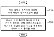
본 발명의 실시예들에 따른 비휘발성 메모리 장치의 데이터 소거 방법에서, 미리 정해진 주기마다 상기 메모리 블록에 대한 데이터 소거 특성이 열화되었는지 판단한다(단계 S100). 상기 데이터 소거 특성이 열화된 것으로 판단된 경우에, 상기 메모리 블록을 소거 대상 블록으로 선택하기 위한 선택 트랜지스터들에 인가되는 전압의 레벨을 변경하여 데이터 소거 동작을 수행한다(단계 S200).In the data erasing method of a nonvolatile memory device according to embodiments of the present invention, it is determined whether data erasing characteristics of the memory block are deteriorated at predetermined intervals (step S100). When it is determined that the data erase characteristics are deteriorated, a data erase operation is performed by changing the level of voltage applied to selection transistors for selecting the memory block as an erase target block (step S200).
상기 데이터 소거 동작은 GIDL(gate induced drain leakage) 방식에 기초하여 수행될 수 있다. 예를 들어, 상기 선택 트랜지스터들의 제1 전극(예를 들어, 드레인 전극)에 상대적으로 높은 전압을 인가하고 상기 선택 트랜지스터들의 제어 전극(예를 들어, 게이트 전극)에 상대적으로 낮은 전압을 인가함으로써, GIDL 현상을 발생시킬 수 있다. 상기 선택 트랜지스터들은 GIDL 주입(injection) 트랜지스터들로 부를 수 있다.The data erase operation may be performed based on a gate induced drain leakage (GIDL) scheme. For example, by applying a relatively high voltage to the first electrodes (eg, drain electrodes) of the selection transistors and applying a relatively low voltage to the control electrodes (eg, gate electrodes) of the selection transistors, GIDL phenomenon can occur. The select transistors may be referred to as GIDL injection transistors.
상기 데이터 소거 특성이 열화되었다는 것은 상기 GIDL 주입 트랜지스터들의 특성이 열화된 것을 나타낼 수 있다. 예를 들어, 상기 GIDL 주입 트랜지스터들의 특성이 열화되었다는 것은 상기 GIDL 주입 트랜지스터들의 문턱 전압이 감소한 것을 나타낼 수 있다. 상기 GIDL 주입 트랜지스터들의 문턱 전압이 감소한 경우에, 도 2에 도시된 것처럼 상기 GIDL 주입 트랜지스터들의 I-V 곡선(curve)이 CASEA에서 CASEB로 변할 수 있다. 이에 따라, 상기 GIDL 주입 트랜지스터들의 게이트 전극의 전압(Vg)이 동일 레벨(예를 들어, Vgidl)로 유지되더라도 드레인 전극의 전류(Id)가 감소할 수 있다. 다시 말하면, 동일 전압 조건에서의 GIDL 발생량이 감소하며, 따라서 상기 GIDL 주입 트랜지스터들의 문턱 전압이 감소한 경우에 상기 데이터 소거 동작이 정상적으로 수행되지 않을 수 있다.The deterioration of the data erasing characteristics may indicate deterioration of characteristics of the GIDL injection transistors. For example, the deterioration of the characteristics of the GIDL injection transistors may indicate that the threshold voltages of the GIDL injection transistors are reduced. When the threshold voltage of the GIDL injection transistors decreases, as shown in FIG. 2 , the I-V curve of the GIDL injection transistors may change from CASEA to CASEB. Accordingly, even if the voltage Vg of the gate electrode of the GIDL injection transistors is maintained at the same level (eg, Vgidl), the current Id of the drain electrode may decrease. In other words, the amount of GIDL generation decreases under the same voltage condition, and thus, the data erase operation may not be normally performed when the threshold voltages of the GIDL injection transistors decrease.
본 발명의 실시예들에 따른 비휘발성 메모리 장치의 데이터 소거 방법에서 상기 데이터 소거 동작을 수행하는데 있어서(단계 S200), 구조적 변경 없이 상기 선택 트랜지스터들에 인가되는 상기 전압의 레벨을 변경하여 GIDL 발생량을 조절함으로써(즉, 상기 GIDL 주입 트랜지스터들에 대한 전압 가변을 통해 GIDL 발생량을 조절함으로써), 상기 데이터 소거 동작의 특성 및 신뢰성을 향상시킬 수 있다.In the method of erasing data of a nonvolatile memory device according to embodiments of the present invention, in performing the data erasing operation (step S200), the level of the voltage applied to the selection transistors is changed without structural change to reduce the amount of GIDL generation. By controlling (that is, by adjusting the amount of GIDL generation by varying the voltage of the GIDL injection transistors), characteristics and reliability of the data erase operation may be improved.
일 실시예에서, 상기 선택 트랜지스터들(즉, 상기 GIDL 주입 트랜지스터들)의 드레인 전극과 게이트 전극의 전압 차이를 조절하여 GIDL 발생량을 조절할 수 있다. 예를 들어, 상기 선택 트랜지스터들의 드레인 전극과 게이트 전극의 전압 차이가 증가할수록 상기 GIDL 발생량은 증가할 수 있다.In an embodiment, the amount of GIDL generation may be adjusted by adjusting a voltage difference between a drain electrode and a gate electrode of the selection transistors (ie, the GIDL injection transistors). For example, as the voltage difference between the drain electrode and the gate electrode of the selection transistors increases, the amount of GIDL generation may increase.
구체적으로, 상기 GIDL 주입 트랜지스터들의 드레인 전극의 전압을 증가시키는 경우에, 도 3a에 도시된 것처럼 상기 GIDL 주입 트랜지스터들의 I-V 곡선이 CASEB에서 CASEC로 변할 수 있다. 이 경우, 상기 GIDL 주입 트랜지스터들의 게이트 전극의 전압(Vg)이 동일 레벨(예를 들어, Vgidl)로 유지되더라도 드레인 전극의 전류(Id)가 증가하며, 이에 따라 상기 GIDL 발생량이 증가할 수 있다. 또한, 상기 GIDL 주입 트랜지스터들의 게이트 전극의 전압을 감소시키는 경우에, 예를 들어 도 3b에 도시된 것처럼 게이트 전극의 전압(Vg)을 Vgidl에서 Vgidl'로 감소시키는 경우에, 드레인 전극의 전류(Id)가 증가하며, 이에 따라 상기 GIDL 발생량이 증가할 수 있다. 추가적으로, 상기 GIDL 주입 트랜지스터들의 드레인 전극의 전압을 증가시키고 이와 함께 게이트 전극의 전압을 감소시키는 경우에도, 상기 GIDL 발생량이 증가할 수 있다. 상기 GIDL 주입 트랜지스터들의 드레인 전극과 게이트 전극의 전압 차이를 조절하는 구체적인 방식은 도 7 내지 16을 참조하여 상세하게 후술하도록 한다.Specifically, when the voltage of the drain electrode of the GIDL injection transistors is increased, the I-V curve of the GIDL injection transistors may change from CASEB to CASEC as shown in FIG. 3A . In this case, even if the voltage Vg of the gate electrode of the GIDL injection transistors is maintained at the same level (eg, Vgidl), the current Id of the drain electrode increases, and accordingly, the amount of GIDL generation may increase. In addition, when the voltage of the gate electrode of the GIDL injection transistors is reduced, for example, when the voltage (Vg) of the gate electrode is reduced from Vgidl to Vgidl' as shown in FIG. 3B, the current (Id) of the drain electrode ) increases, and accordingly, the amount of GIDL generation may increase. Additionally, when the voltage of the drain electrode of the GIDL injection transistors is increased and the voltage of the gate electrode is decreased together with the increase, the amount of GIDL generation may be increased. A specific method of adjusting the voltage difference between the drain electrode and the gate electrode of the GIDL injection transistors will be described later in detail with reference to FIGS. 7 to 16 .
일 실시예에서, 상기 데이터 소거 특성이 열화되었는지 판단하는 상기 미리 정해진 주기는 상기 데이터 소거 동작의 수행 횟수(즉, 프로그램/소거 사이클의 수행 횟수)와 관련될 수 있다. 상기 데이터 소거 동작의 수행 횟수가 증가할수록 상기 데이터 소거 특성의 열화(즉, 상기 GIDL 주입 트랜지스터들의 문턱 전압의 감소)는 심해지며, 따라서 상기 데이터 소거 동작이 I(I는 2 이상의 자연수)회 수행될 때마다 상기 데이터 소거 특성이 열화되었는지 판단할 수 있다. 예를 들어, I=100인 경우에, 상기 데이터 소거 동작이 100회, 200회, 300회 ... 수행될 때마다 상기 데이터 소거 특성이 열화되었는지 판단할 수 있다.In an embodiment, the predetermined cycle for determining whether the data erase characteristics are deteriorated may be related to the number of times the data erase operation is performed (ie, the number of program/erase cycles performed). As the number of times the data erase operation is performed increases, the deterioration of the data erase characteristic (that is, the decrease in the threshold voltage of the GIDL injection transistors) becomes severe, and thus the data erase operation is performed I (where I is a natural number greater than or equal to 2) times. Each time, it may be determined whether the data erasing characteristics are deteriorated. For example, in the case of I=100, it may be determined whether the data erasing characteristics are deteriorated every time the data erasing operation is performed 100 times, 200 times, 300 times, and so on.
다른 실시예에서, 상기 데이터 소거 특성이 열화되었는지 판단하는 상기 미리 정해진 주기는 상기 비휘발성 메모리 장치의 동작 환경의 온도 및/또는 구동 시간과 관련될 수 있다. 상기 동작 환경의 온도가 상대적으로 낮은 저온 환경 또는 상대적으로 높은 고온 환경에서 상기 데이터 소거 특성의 열화(즉, 상기 GIDL 주입 트랜지스터들의 문턱 전압의 감소)는 심해지며, 상기 저온 환경 또는 상기 고온 환경에서의 구동 시간이 J(J는 양의 실수)시간 경과할 때마다 상기 데이터 소거 특성이 열화되었는지 판단할 수 있다.In another embodiment, the predetermined cycle for determining whether the data erase characteristics are deteriorated may be related to a temperature of an operating environment and/or an operating time of the nonvolatile memory device. In a low-temperature environment in which the temperature of the operating environment is relatively low or in a high-temperature environment where the temperature of the operating environment is relatively high, the deterioration of the data erasing characteristic (that is, the decrease in the threshold voltage of the GIDL injection transistors) becomes severe, and in the low-temperature environment or the high-temperature environment It may be determined whether the data erasing characteristics are deteriorated whenever the driving time elapses by J (where J is a positive real number).
또 다른 실시예에서, 상기 데이터 소거 특성이 열화되었는지 판단하는 상기 미리 정해진 주기는 상기 데이터 소거 특성의 열화를 유발하는 다양한 요인들 중 적어도 하나와 관련될 수 있다.In another embodiment, the predetermined cycle for determining whether the data erasing characteristics are degraded may be related to at least one of various factors causing deterioration of the data erasing characteristics.
한편, 본 발명의 실시예들에 따른 비휘발성 메모리 장치의 데이터 소거 방법은 데이터 소거 동작을 수행하기 위한 커맨드 및 어드레스에 기초하여(예를 들어, 커맨드 및 어드레스가 수신되면) 수행될 수 있다.Meanwhile, a data erasing method of a nonvolatile memory device according to embodiments of the present invention may be performed based on a command and an address for performing a data erasing operation (eg, when a command and an address are received).
도 4는 본 발명의 실시예들에 따른 비휘발성 메모리 장치를 나타내는 블록도이다.4 is a block diagram illustrating a non-volatile memory device according to example embodiments.
도 4를 참조하면, 비휘발성 메모리 장치(100)는 메모리 셀 어레이(110), 로우 디코더(120), 페이지 버퍼 회로(130), 데이터 입출력 회로(140), 전압 발생기(150) 및 제어 회로(160)를 포함한다.Referring to FIG. 4 , the
메모리 셀 어레이(110)는 복수의 스트링 선택 라인들(SSL), 복수의 워드 라인들(WL) 및 복수의 접지 선택 라인들(GSL)을 통해 로우 디코더(120)와 연결된다. 또한, 메모리 셀 어레이(110)는 복수의 비트 라인들(BL)을 통해 페이지 버퍼 회로(130)와 연결된다. 메모리 셀 어레이(110)는 복수의 워드 라인들(WL) 및 복수의 비트 라인들(BL)에 연결되는 복수의 메모리 셀들을 포함할 수 있다. 메모리 셀 어레이(110)는 각각 메모리 셀들을 포함하는 복수의 메모리 블록들(BLK1, BLK2, ..., BLKz)로 구분될 수 있다.The
일 실시예에서, 도 5 및 6을 참조하여 후술하는 것처럼, 메모리 셀 어레이(110)는 기판 상에 삼차원 구조(또는 수직 구조)로 형성되는 삼차원(three dimensional) 메모리 셀 어레이일 수 있다. 이 경우, 메모리 셀 어레이(110)는 서로 적층되어 형성되는 복수의 메모리 셀들을 포함하는 셀 스트링들, 예를 들어 수직 메모리 낸드 스트링들을 포함할 수 있다.In one embodiment, as described below with reference to FIGS. 5 and 6 , the
제어 회로(160)는 메모리 컨트롤러(예를 들어, 도 30의 600)로부터 커맨드(CMD) 및 어드레스(ADDR)를 수신하고, 커맨드(CMD) 및 어드레스(ADDR)에 기초하여 비휘발성 메모리 장치(100)의 소거 루프, 프로그램 루프 및 독출 동작을 제어한다.The
예를 들어, 제어 회로(160)는 커맨드(CMD)에 기초하여 전압 발생기(150)를 제어하기 위한 제어 신호들(CON) 및 페이지 버퍼 회로(130)를 제어하기 위한 제어 신호들(PBC)을 발생하고, 어드레스(ADDR)에 기초하여 로우 어드레스(R_ADDR) 및 컬럼 어드레스(C_ADDR)를 발생할 수 있다. 제어 회로(160)는 로우 어드레스(R_ADDR)를 로우 디코더(120)에 제공하고, 컬럼 어드레스(C_ADDR)를 데이터 입출력 회로(140)에 제공할 수 있다.For example, the
또한, 제어 회로(160)는 본 발명의 실시예들에 따른 데이터 소거 방법을 수행하도록 로우 디코더(120), 페이지 버퍼 회로(130), 데이터 입출력 회로(140) 및 전압 발생기(150)를 제어할 수 있다.In addition, the
로우 디코더(120)는 복수의 스트링 선택 라인들(SSL), 복수의 워드 라인들(WL) 및 복수의 접지 선택 라인들(GSL)을 통해 메모리 셀 어레이(110)와 연결된다.The
예를 들어, 소거/프로그램/독출 동작 시에, 로우 디코더(120)는 로우 어드레스(R_ADDR)에 응답하여, 복수의 워드 라인들(WL) 중 적어도 하나를 선택 워드 라인으로 결정하고, 복수의 워드 라인들(WL) 중에서 상기 선택 워드 라인을 제외한 나머지 워드 라인들을 비선택 워드 라인들로 결정할 수 있다. 또한, 복수의 스트링 선택 라인들(SSL) 중 적어도 하나를 선택 스트링 선택 라인으로 결정하고, 나머지 스트링 선택 라인들을 비선택 스트링 선택 라인들로 결정할 수 있다. 추가적으로, 복수의 접지 선택 라인들(GSL) 중 적어도 하나를 선택 접지 선택 라인으로 결정하고, 나머지 접지 선택 라인들을 비선택 접지 선택 라인들로 결정할 수 있다.For example, during an erase/program/read operation, the
전압 발생기(150)는 전원 전압(PWR) 및 제어 신호들(CON)에 기초하여 비휘발성 메모리 장치(100)의 동작에 필요한 워드 라인 전압들(VWL)을 발생할 수 있다. 워드 라인 전압들(VWL)은 로우 디코더(120)를 통해 복수의 스트링 선택 라인들(SSL), 복수의 워드 라인들(WL) 및 복수의 접지 선택 라인들(GSL)에 인가될 수 있다. 또한, 전압 발생기(150)는 전원 전압(PWR) 및 제어 신호들(CON)에 기초하여 소거 동작에 필요한 소거 전압(VERS)을 발생할 수 있다.The
예를 들어, 소거 동작 시에, 전압 발생기(150)는 메모리 블록들(BLK1~BLKz)의 공통 소스 라인(CSL) 및/또는 비트 라인들(BL)에 소거 전압(VERS)을 인가하고, 로우 디코더(120)를 통해 하나의 메모리 블록의 모든 워드 라인들 또는 일부의 서브 블록에 해당하는 워드 라인들에 소거 허용 전압(예를 들어, 접지 전압)을 인가할 수 있다. 소거 검증 동작 시에, 전압 발생기(150)는 하나의 메모리 블록의 모든 워드 라인들에 소거 검증 전압을 인가하거나 워드 라인 단위로 소거 검증 전압을 인가할 수 있다.For example, during an erase operation, the
페이지 버퍼 회로(130)는 복수의 비트 라인들(BL)을 통해 메모리 셀 어레이(110)와 연결될 수 있다. 페이지 버퍼 회로(130)는 복수의 페이지 버퍼들을 포함할 수 있다. 일 실시예에서, 하나의 페이지 버퍼에 하나의 비트 라인이 연결될 수 있다. 다른 실시예에서, 하나의 페이지 버퍼에 두 개 이상의 비트 라인들이 연결될 수 있다.The
페이지 버퍼 회로(130)는 메모리 셀 어레이(110)에 프로그램 될 기입 데이터(DAT)를 저장하거나 혹은 메모리 셀 어레이(110)로부터 감지된 독출 데이터(DAT)를 저장할 수 있다. 즉, 페이지 버퍼 회로(130)는 비휘발성 메모리 장치(100)의 동작 모드에 따라 기입 드라이버로서 또는 감지 증폭기로서 동작할 수 있다.The
데이터 입출력 회로(140)는 데이터 라인들(DL)을 통해 페이지 버퍼 회로(130)와 연결될 수 있다. 데이터 입출력 회로(140)는 컬럼 어드레스(C_ADDR)에 응답하여, 기입 데이터(DAT)를 페이지 버퍼 회로(130)를 거쳐서 메모리 셀 어레이(110)에 제공하거나 혹은 메모리 셀 어레이(110)로부터 페이지 버퍼 회로(130)를 거쳐서 출력되는 독출 데이터(DAT)를 외부(예를 들어, 도 30의 메모리 컨트롤러(600))에 제공할 수 있다.The data input/
도 5는 도 4의 비휘발성 메모리 장치의 메모리 셀 어레이에 포함되는 메모리 블록의 일 예를 나타내는 사시도이다.FIG. 5 is a perspective view illustrating an example of a memory block included in a memory cell array of the nonvolatile memory device of FIG. 4 .
도 5를 참조하면, 메모리 블록(BLKi)은 3차원 구조 또는 수직 구조로 형성되는 낸드 스트링들을 포함한다. 메모리 블록(BLKi)은 복수의 방향들(D1, D2, D3)을 따라 신장된 구조물들을 포함한다.Referring to FIG. 5 , the memory block BLKi includes NAND strings formed in a 3D structure or a vertical structure. The memory block BLKi includes structures extending along a plurality of directions D1 , D2 , and D3 .
메모리 블록(BLKi)을 형성하기 위해서는, 우선 기판(111)이 제공된다. 예를 들어, 기판(111)은 붕소(B, boron)와 같은 5족 원소가 주입되어 형성된 P-웰로 형성될 수 있다. 또는, 기판(111)은 N-웰 내에 제공되는 포켓 P-웰로 형성될 수 있다. 이하에서, 기판(111)은 P-웰인 것으로 가정한다. 그러나 기판(111)은 P-웰에만 한정되지 않는다.To form the memory block BLKi, a
기판(111) 상에, 제1 방향(D1)을 따라 복수의 도핑 영역들(311, 312, 313, 314)이 형성된다. 예를 들어, 복수의 도핑 영역들(311~314)은 기판(111)과 상이한 N-타입의 도전체로 형성될 수 있다. 이하에서, 복수의 도핑 영역들(311~314)은 N-타입을 갖는 것으로 가정한다. 그러나 복수의 도핑 영역들(311~314)은 N-타입을 갖는 것으로만 한정되지 않는다.On the
도핑 영역들(311, 312) 사이의 기판(111) 상에, 제2 방향(D2)을 따라 신장되는 복수의 절연 물질들(112)이 제3 방향(D3)을 따라 순차적으로 제공된다. 예를 들어, 복수의 절연 물질들(112)은 제3 방향(D3)을 따라 특정 거리만큼 이격되어 형성될 수 있다. 예를 들어, 복수의 절연 물질들(112)은 실리콘 산화물(silicon oxide)과 같은 절연 물질을 포함할 수 있다.On the
도핑 영역들(311, 312) 사이의 기판(111) 상에, 제2 방향(D2)을 따라 순차적으로 배치되며 제3 방향(D3)을 따라 복수의 절연 물질들(112)을 관통하는 복수의 필라들(113)이 형성된다. 예를 들어, 복수의 필라들(113)은 복수의 절연 물질들(112)을 관통하여 기판(111)과 연결될 수 있다. 또한, 복수의 필라들(113)은 도핑 영역들(312, 313) 사이의 기판 상에, 및 도핑 영역들(313, 314) 사이의 기판 상에도 형성된다.On the
일 실시예에서, 각 필라(113)는 복수의 물질들로 구성될 수 있다. 예를 들어, 각 필라(113)의 표면층(114)은 제1 타입을 갖는 실리콘 물질을 포함할 수 있고, 낸드 스트링의 채널이 형성되는 영역으로 기능할 수 있다. 예를 들어, 각 필라(113)의 표면층(114)은 기판(111)과 동일한 타입을 갖는 실리콘 물질을 포함할 수 있다. 이하에서, 각 필라(113)의 표면층(114)은 P-타입 실리콘을 포함하는 것으로 가정한다. 그러나 각 필라(113)의 표면층(114)은 P-타입 실리콘을 포함하는 것으로 한정되지 않는다.In one embodiment, each
각 필라(113)의 내부층(115)은 절연 물질로 구성된다. 예를 들어, 각 필라(113)의 내부층(115)은 실리콘 산화물(silicon oxide)과 같은 절연 물질을 포함할 수 있다. 예를 들어, 각 필라(113)의 내부층(115)은 에어 갭(air gap)을 포함할 수 있다.The
도핑 영역들(311, 312) 사이의 영역에서, 복수의 절연 물질들(112), 복수의 필라들(113), 그리고 기판(111)의 노출된 표면을 따라 절연막(116)이 제공된다. 예를 들어, 제3 방향(D3)을 따라 제공되는 마지막 절연 물질(112)의 제3 방향(D3) 쪽의 노출면에 제공되는 절연막(116)은 제거될 수 있다.In a region between the
도핑 영역들(311, 312) 사이의 영역에서, 절연막(116)의 노출된 표면상에 복수의 제1 도전 물질들(211, 221, 231, 241, 251, 261, 271, 281, 291)이 제공된다. 예를 들어, 기판(111)에 인접한 절연 물질(112) 및 기판(111) 사이에 제2 방향(D2)을 따라 신장되는 제1 도전 물질(211)이 제공될 수 있다. 구체적으로, 기판(111)에 인접한 절연 물질(112)의 하부면의 절연막(116) 및 기판(111) 사이에, 제2 방향(D2)으로 신장되는 제1 도전 물질(211)이 제공될 수 있다.A plurality of first
절연 물질들(112) 중 특정 절연 물질 상부면의 절연막(116) 및 특정 절연 물질 상부에 배치된 절연 물질의 하부면의 절연막(116) 사이에, 제2 방향(D2)을 따라 신장되는 제1 도전 물질이 제공된다. 예를 들어, 절연 물질들(112) 사이에, 제2 방향(D2)으로 신장되는 제1 도전 물질들(221~281)이 제공될 수 있다. 예를 들어, 제1 도전 물질들(211~291)은 금속 물질일 수 있다. 예를 들어, 제1 도전 물질들(211~291)은 폴리 실리콘 등과 같은 도전 물질들일 수 있다.A first layer extending along the second direction D2 between the insulating
도핑 영역들(312, 313) 사이의 영역에서, 도핑 영역들(311, 312) 사이의 영역 상의 구조물과 동일한 구조물이 제공될 수 있다. 또한, 도핑 영역들(313, 314) 사이의 영역에서, 도핑 영역들(311, 312) 사이의 영역 상의 구조물과 동일한 구조물이 제공될 수 있다.In the region between the
복수의 필라들(113) 상에 복수의 드레인들(320)이 각각 제공된다. 드레인들(320) 상에, 제1 방향(D1)으로 신장된 복수의 제2 도전 물질들(331, 332, 333)이 제공된다. 제2 도전 물질들(331~333)은 제2 방향(D2)을 따라 순차적으로 배치된다. 제2 도전 물질들(331~333) 각각은 대응하는 영역의 드레인(320)과 연결된다. 예를 들어, 드레인들(320) 및 제1 방향(D1)으로 신장된 제2 도전 물질들(331~333)은 각각 콘택 플러그들(contact plug)을 통해 연결될 수 있다. 예를 들어, 제2 도전 물질들(331~333)은 금속 물질들일 수 있다. 예를 들어, 제2 도전 물질들(331~333)은 폴리 실리콘 등과 같은 도전 물질들일 수 있다.A plurality of
도 5의 예에서, 제1 도전 물질들(211~291)은 워드 라인들(WL), 스트링 선택 라인들(SSL) 및 접지 선택 라인들(GSL)을 형성할 수 있다. 제1 도전 물질들(211~291) 중에서 워드 라인들(WL)을 형성하는 일부(예를 들어, 231~271)는 동일한 층에 속한 것들은 상호 연결될 수 있다. 제2 도전 물질들(331~333)은 비트 라인들(BL)을 형성할 수 있다.In the example of FIG. 5 , the first
도 6은 도 5를 참조하여 설명된 메모리 블록의 등가 회로를 나타내는 회로도이다.FIG. 6 is a circuit diagram illustrating an equivalent circuit of the memory block described with reference to FIG. 5 .
도 6에 도시된 메모리 블록(BLKi)은 기판 상에 삼차원 구조로 형성되는 삼차원 메모리 블록을 나타낸다. 예를 들어, 메모리 블록(BLKi)에 포함되는 복수의 메모리 낸드 스트링들은 상기 기판과 수직한 방향으로 형성될 수 있다.The memory block BLKi shown in FIG. 6 represents a three-dimensional memory block formed in a three-dimensional structure on a substrate. For example, a plurality of memory NAND strings included in the memory block BLKi may be formed in a direction perpendicular to the substrate.
도 6을 참조하면, 메모리 블록(BLKi)은 비트 라인들(BL1, BL2, BL3)과 공통 소스 라인(CSL) 사이에 연결되는 복수의 메모리 낸드 스트링들(NS11, NS12, NS13, NS21, NS22, NS23, NS31, NS32, NS33)을 포함할 수 있다. 복수의 메모리 낸드 스트링들(NS11~NS33) 각각은 복수의 스트링 선택 트랜지스터들(SST1, SST2), 복수의 메모리 셀들(MC1, MC2, MC3, MC4, MC5, MC6) 및 복수의 접지 선택 트랜지스터들(GST1, GST2)을 포함할 수 있다. 예를 들어, 비트 라인들(BL1~BL3)은 도 5의 제2 도전 물질들(331~333)에 대응할 수 있고, 도 5의 도핑 영역들(311~314)이 서로 연결되어 공통 소스 라인(CSL)을 형성할 수 있다.Referring to FIG. 6 , the memory block BLKi includes a plurality of memory NAND strings NS11, NS12, NS13, NS21, NS22, NS23, NS31, NS32, NS33) may be included. Each of the plurality of memory NAND strings NS11 to NS33 includes a plurality of string selection transistors SST1 and SST2, a plurality of memory cells MC1, MC2, MC3, MC4, MC5, and MC6, and a plurality of ground selection transistors ( GST1, GST2) may be included. For example, the bit lines BL1 to BL3 may correspond to the second
스트링 선택 트랜지스터들(SST1, SST2)은 상응하는 스트링 선택 라인들(SSL11, SSL12, SSL13, SSL21, SSL22, SSL23)에 연결될 수 있다. 복수의 메모리 셀들(MC1~MC6)은 각각 상응하는 워드 라인(WL1, WL2, WL3, WL4, WL5, WL6)에 연결될 수 있다. 접지 선택 트랜지스터들(GST1, GST2)은 상응하는 접지 선택 라인들(GSL11, GSL21, GSL22, GSL23)에 연결될 수 있다. 가장 상단의 스트링 선택 트랜지스터(SST2)는 상응하는 비트 라인(BL1, BL2, BL3)에 연결되고, 가장 하단의 접지 선택 트랜지스터(GST1)는 공통 소스 라인(CSL)에 연결될 수 있다.The string select transistors SST1 and SST2 may be connected to corresponding string select lines SSL11 , SSL12 , SSL13 , SSL21 , SSL22 and SSL23 . The plurality of memory cells MC1 to MC6 may be connected to corresponding word lines WL1 , WL2 , WL3 , WL4 , WL5 , and WL6 , respectively. The ground select transistors GST1 and GST2 may be connected to corresponding ground select lines GSL11, GSL21, GSL22 and GSL23. The uppermost string select transistor SST2 may be connected to the corresponding bit lines BL1 , BL2 , and BL3 , and the lowermost ground select transistor GST1 may be connected to the common source line CSL.
동일한 층의 워드 라인(예를 들면, WL1)은 공통으로 연결되고, 접지 선택 라인(GSL11)은 공통으로 연결되며, 접지 선택 라인들(GSL21, GSL22, GSL23) 및 스트링 선택 라인들(SSL11, SSL12, SSL13, SSL21, SSL22, SSL23)은 각각 분리될 수 있다. 동일한 반도체 층의 메모리 셀들은 워드 라인을 공유하고, 동일한 행의 셀 스트링들은 스트링 선택 라인을 공유하며, 공통 소스 라인(CSL)은 모든 셀 스트링들에 공통으로 연결될 수 있다.A word line (eg, WL1) of the same layer is connected in common, a ground select line (GSL11) is connected in common, ground select lines (GSL21, GSL22, GSL23) and string select lines (SSL11, SSL12) , SSL13, SSL21, SSL22, SSL23) can be separated respectively. Memory cells of the same semiconductor layer may share a word line, cell strings of the same row may share a string select line, and a common source line CSL may be commonly connected to all cell strings.
수직형(또는 3차원) 메모리 셀 어레이에 대한 자세한 설명은 본 명세서에 참고 문헌으로 결합된 미국 등록 번호 7,679,133; 8,553,466; 8,654,587; 8,559,235 및 미국 공개 번호 2011/0233648에 기술되어 있다.A detailed description of vertical (or three-dimensional) memory cell arrays can be found in US Registration Nos. 7,679,133; 8,553,466; 8,654,587; 8,559,235 and US Publication No. 2011/0233648.
한편, NAND 플래시 메모리 장치에 기초하여 본 발명의 실시예들에 따른 비휘발성 메모리 장치에 포함되는 메모리 셀 어레이 및 메모리 블록을 설명하였으나, 본 발명의 실시예들에 따른 비휘발성 메모리 장치는 PRAM(Phase Change Random Access Memory), RRAM(Resistance Random Access Memory), NFGM(Nano Floating Gate Memory), PoRAM(Polymer Random Access Memory), MRAM(Magnetic Random Access Memory), FRAM(Ferroelectric Random Access Memory) 등과 같은 임의의 비휘발성 메모리 장치일 수 있다.Meanwhile, a memory cell array and a memory block included in a nonvolatile memory device according to embodiments of the present invention have been described based on a NAND flash memory device, but a nonvolatile memory device according to embodiments of the present invention is PRAM (Phase Change Random Access Memory), Resistance Random Access Memory (RRAM), Nano Floating Gate Memory (NFGM), Polymer Random Access Memory (PoRAM), Magnetic Random Access Memory (MRAM), Ferroelectric Random Access Memory (FRAM), etc. It may be a volatile memory device.
도 7은 본 발명의 실시예들에 따른 메모리 블록을 나타내는 회로도이다.7 is a circuit diagram illustrating a memory block according to example embodiments.
도 7에는 편의상 하나의 비트 라인(BL)에 연결되는 복수의 셀 스트링들(STR1, STR2, STR3, STR4)이 도시되어 있다. 도 5 및 6을 참조하여 전술한 바와 같이, 제2 방향(D2)으로 신장된 복수의 비트 라인들이 제1 방향(D1)으로 배열될 수 있다.7 illustrates a plurality of cell strings STR1 , STR2 , STR3 , and STR4 connected to one bit line BL for convenience. As described above with reference to FIGS. 5 and 6 , a plurality of bit lines extending in the second direction D2 may be arranged in the first direction D1 .
도 7을 참조하면, 비휘발성 메모리 장치의 메모리 블록은 복수의 셀 스트링들(STR1~STR4)을 포함하고, 복수의 셀 스트링들(STR1~STR4)의 각각은 수직 방향 또는 제3 방향(D1)으로 배치되는 복수의 메모리 셀들을 포함한다.Referring to FIG. 7 , the memory block of the non-volatile memory device includes a plurality of cell strings STR1 to STR4, and each of the plurality of cell strings STR1 to STR4 extends in a vertical direction or in a third direction D1. It includes a plurality of memory cells arranged in
복수의 게이트 라인 층들에는 스트링 선택 라인들(SSL0u, SSL1u, SSL2u, SSL3u, SSL0d, SSL1d, SSL2d, SSL3d), 워드 라인들(WL0, WL1, WL2, ..., WL(K-1), WLK) 및 접지 선택 라인들(GSLd, GSL0u, GSL1u, GSL2u, GSL3u)이 형성될 수 있다. 실시예에 따라서, 인접한 워드 라인들 사이에 적어도 하나의 더미 워드 라인이 배치될 수도 있고, 하부 스트링 선택 라인들(SSL0d~SSL3d) 및 상부 접지 선택 라인들(GSL0u~GSL3u) 중 적어도 하나는 생략될 수도 있다.The plurality of gate line layers include string select lines (SSL0u, SSL1u, SSL2u, SSL3u, SSL0d, SSL1d, SSL2d, SSL3d), word lines (WL0, WL1, WL2, ..., WL(K-1), WLK ) and ground selection lines GSLd, GSL0u, GSL1u, GSL2u, and GSL3u may be formed. Depending on embodiments, at least one dummy word line may be disposed between adjacent word lines, and at least one of the lower string select lines SSL0d to SSL3d and the upper ground select lines GSL0u to GSL3u may be omitted. may be
일 실시예에서, 도 8 내지 13b를 참조하여 후술하는 것처럼, 소거 전압(VERS)은 공통 소스 라인(CSL)에 인가될 수 있으며, 이 경우 공통 소스 라인(CSL)과 직접 연결되고 하부 접지 선택 라인(GSLd)과 연결된 접지 선택 트랜지스터들이 도 1의 단계 S200에서의 상기 선택 트랜지스터들에 대응할 수 있다. 다른 실시예에서, 도 14 내지 16을 참조하여 후술하는 것처럼, 소거 전압(VERS)은 비트 라인(BL)에 인가될 수 있으며, 이 경우 비트 라인(BL)과 직접 연결되고 상부 스트링 선택 라인들(SSL0u~SSL3u)과 연결된 스트링 선택 트랜지스터들이 도 1의 단계 S200에서의 상기 선택 트랜지스터들에 대응할 수 있다.In one embodiment, as described below with reference to FIGS. 8 to 13B , the erase voltage VERS may be applied to the common source line CSL, in which case it is directly connected to the common source line CSL and the lower ground select line. Ground selection transistors connected to (GSLd) may correspond to the selection transistors in step S200 of FIG. 1 . In another embodiment, as will be described later with reference to FIGS. 14 to 16 , the erase voltage VERS may be applied to the bit line BL, in which case it is directly connected to the bit line BL and the upper string select lines ( The string selection transistors connected to SSL0u to SSL3u) may correspond to the selection transistors in step S200 of FIG. 1 .
도 8은 도 1의 데이터 소거 동작을 수행하는 단계의 일 예를 나타내는 순서도이다. 도 9a 및 9b는 도 8의 데이터 소거 동작을 설명하기 위한 도면들이다.FIG. 8 is a flowchart illustrating an example of performing the data erase operation of FIG. 1 . 9A and 9B are diagrams for explaining the data erase operation of FIG. 8 .
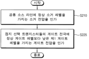
도 7, 8, 9a 및 9b를 참조하면, 상기 데이터 소거 동작을 수행하는데 있어서, 메모리 블록의 공통 소스 라인(CSL)에 정상 소거 레벨(VERSN)을 가지는 소거 전압(VERS)을 인가할 수 있다(단계 S210).7, 8, 9a and 9b, in performing the data erase operation, an erase voltage VERS having a normal erase level VERSN may be applied to a common source line CSL of a memory block ( Step S210).
예를 들어, 도 9a에 도시된 것처럼, 공통 소스 라인(CSL)에 인가되는 소거 전압(VERS)의 레벨은 시간 T1에서 정상 소거 레벨(VERSN)보다 낮은 정상 GIDL 소거 레벨(VGERSN)을 가지고, 시간 T2에서 증가하여 시간 T3에서 정상 소거 레벨(VERSN)을 가질 수 있다. 다른 예에서, 도 9b에 도시된 것처럼, 공통 소스 라인(CSL)에 인가되는 소거 전압(VERS)의 레벨은 시간 TA에서 증가하여 시간 TB에서 정상 소거 레벨(VERSN)을 가질 수 있다. 도 9a의 시간 T3 및 도 9b의 시간 TB가 상기 데이터 소거 동작이 실제로 수행되는 구간을 나타낼 수 있다.For example, as shown in FIG. 9A , the level of the erase voltage VERS applied to the common source line CSL has a normal GIDL erase level VGERSN lower than the normal erase level VERSN at time T1, and It may increase at T2 and have a normal erase level (VERSN) at time T3. In another example, as shown in FIG. 9B , the level of the erase voltage VERS applied to the common source line CSL may increase at time TA to have a normal erase level VERSN at time TB. Time T3 of FIG. 9A and time TB of FIG. 9B may indicate a period in which the data erase operation is actually performed.
공통 소스 라인(CSL)에 소거 전압(VERS)을 인가하는 동안에, 공통 소스 라인(CSL)과 직접 연결되고 하부 접지 선택 라인(GSLd)과 연결된 상기 접지 선택 트랜지스터들의 게이트 전극(즉, 하부 접지 선택 라인(GSLd))에 정상 게이트 레벨(VGN)보다 낮은 제1 게이트 레벨(VGN-ΔVG)을 가지는 게이트 전압을 인가할 수 있다(단계 S225).While the erase voltage VERS is applied to the common source line CSL, the gate electrodes of the ground select transistors directly connected to the common source line CSL and connected to the lower ground select line GSLd (that is, the lower ground select line A gate voltage having a first gate level (VGN-ΔVG) lower than the normal gate level (VGN) may be applied to (GSLd) (step S225).
예를 들어, 도 9a 및 9b에 점선으로 도시된 것처럼, 상기 데이터 소거 특성이 열화되지 않은 경우에 하부 접지 선택 라인(GSLd)에 인가되는 상기 게이트 전압의 레벨은 시간 T2 및 TA에서 증가하여 시간 T3 및 TB에서 정상 게이트 레벨(VGN)을 가질 수 있다. 도 9a 및 9b에 실선으로 도시된 것처럼, 상기 데이터 소거 특성이 열화된 경우에 하부 접지 선택 라인(GSLd)에 인가되는 상기 게이트 전압의 레벨은 시간 T2 및 TA에서 증가하여 시간 T3 및 TB에서 제1 게이트 레벨(VGN-ΔVG)을 가질 수 있다. 이 때, 도 9a 및 9b에 도시된 것처럼 상기 게이트 전압의 증가량(즉, 증가되는 기울기)을 동일하게 유지하면서 상기 게이트 전압의 인가 시점을 지연시키는 방식으로 상기 게이트 전압의 레벨을 감소시킬 수도 있고, 도시하지는 않았지만 상기 게이트 전압의 인가 시점을 동일하게 유지하면서 상기 게이트 전압의 증가량을 변경(예를 들어, 감소)하는 방식으로 상기 게이트 전압의 레벨을 감소시킬 수도 있다.For example, as shown by dotted lines in FIGS. 9A and 9B , when the data erasing characteristics are not deteriorated, the level of the gate voltage applied to the lower ground select line GSLd increases at times T2 and TA to increase at times T3 and a normal gate level (VGN) at TB. As shown by solid lines in FIGS. 9A and 9B , when the data erasing characteristics are degraded, the level of the gate voltage applied to the lower ground select line GSLd increases at times T2 and TA and reaches a first level at times T3 and TB. It may have a gate level (VGN-ΔVG). At this time, as shown in FIGS. 9A and 9B , the level of the gate voltage may be reduced by delaying the application time of the gate voltage while maintaining the same increase in the gate voltage (ie, increased slope), Although not shown, the level of the gate voltage may be reduced by changing (eg, decreasing) the amount of increase of the gate voltage while maintaining the same timing at which the gate voltage is applied.
일 실시예에서, 상기 게이트 전압의 변화량(ΔVG)은 상기 데이터 소거 특성의 열화 정도에 따라 결정되고, 상기 열화 정도가 심할수록 증가할 수 있으며, 이에 대해서는 도 17 내지 22를 참조하여 후술하도록 한다.In one embodiment, the amount of change (ΔVG) of the gate voltage is determined according to the degree of deterioration of the data erasure characteristics, and may increase as the degree of deterioration increases, which will be described later with reference to FIGS. 17 to 22 .
시간 T3 및 TB 동안 공통 소스 라인(CSL)에 정상 소거 레벨(VERSN)을 가지는 소거 전압(VERS)을 인가하고 하부 접지 선택 라인(GSLd)에 제1 게이트 레벨(VGN-ΔVG)을 가지는 상기 게이트 전압을 인가함에 따라, 상기 접지 선택 트랜지스터들의 드레인 전극과 게이트 전극의 전압 차이가 증가하며, 따라서 상기 데이터 소거 동작이 효과적으로 수행될 수 있다. 다시 말하면, 도 8, 9a 및 9b의 실시예는 GIDL 주입 트랜지스터들의 게이트 전압을 감소시켜 GIDL 발생량을 증가시키는 도 3b의 예에 대응할 수 있다.During times T3 and TB, the erase voltage VERS having the normal erase level VERSN is applied to the common source line CSL and the gate voltage having the first gate level VGN-ΔVG is applied to the lower ground select line GSLd. As the voltage difference between the drain and gate electrodes of the ground selection transistors increases, the data erasing operation can be effectively performed. In other words, the embodiments of FIGS. 8, 9a and 9b may correspond to the example of FIG. 3b in which the amount of GIDL generation is increased by reducing the gate voltage of the GIDL injection transistors.
이 때, 상기 접지 선택 트랜지스터들은 하나의 하부 접지 선택 라인(GSLd)과 공통적으로 연결되어 있으므로, 모든 셀 스트링들(STR1~STR4)에 대하여 동일한 전압 조건으로 상기 데이터 소거 동작이 수행될 수 있다.In this case, since the ground select transistors are commonly connected to one lower ground select line GSLd, the data erase operation may be performed on all cell strings STR1 to STR4 under the same voltage condition.
상술한 데이터 소거 동작이 완료되면 시간 T4 및 TC에서 소거 전압(VERS) 및 상기 게이트 전압이 감소할 수 있다.When the above-described data erase operation is completed, the erase voltage VERS and the gate voltage may decrease at times T4 and TC.
한편, 상기 데이터 소거 동작이 수행되는 동안에, 워드 라인들(WL)에는 소거 허용 전압(VERSWL)을 인가할 수 있고, 채널(CH) 내의 전압 변화 파형은 소거 전압(VERS)의 파형과 실질적으로 동일할 수 있다.Meanwhile, while the data erase operation is being performed, the erase allowable voltage VERSWL may be applied to the word lines WL, and the waveform of the voltage change in the channel CH is substantially the same as that of the erase voltage VERS. can do.
도 10은 도 1의 데이터 소거 동작을 수행하는 단계의 다른 예를 나타내는 순서도이다. 도 11a 및 11b는 도 10의 데이터 소거 동작을 설명하기 위한 도면들이다. 이하 도 8, 9a 및 9b와 중복되는 설명은 생략한다.FIG. 10 is a flowchart illustrating another example of performing the data erase operation of FIG. 1 . 11A and 11B are diagrams for explaining a data erase operation of FIG. 10 . Descriptions overlapping those of FIGS. 8, 9a and 9b will be omitted.
도 7, 10, 11a 및 11b를 참조하면, 상기 데이터 소거 동작을 수행하는데 있어서, 메모리 블록의 공통 소스 라인(CSL)에 정상 소거 레벨(VERSN)보다 높은 제1 소거 레벨(VERSN+ΔVE)을 가지는 소거 전압(VERS)을 인가할 수 있다(단계 S215).7, 10, 11a and 11b, in performing the data erase operation, the common source line CSL of the memory block has a first erase level VERSN+ΔVE higher than the normal erase level VERSN. The erase voltage VERS may be applied (step S215).
예를 들어, 도 11a에 점선으로 도시된 것처럼, 상기 데이터 소거 특성이 열화되지 않은 경우에 공통 소스 라인(CSL)에 인가되는 소거 전압(VERS)의 레벨은 시간 T1에서 정상 GIDL 소거 레벨(VGERSN)을 가지고, 시간 T2에서 증가하여 시간 T3에서 정상 소거 레벨(VERSN)을 가질 수 있다. 도 11a에 실선으로 도시된 것처럼, 상기 데이터 소거 특성이 열화된 경우에 공통 소스 라인(CSL)에 인가되는 소거 전압(VERS)의 레벨은 시간 T1에서 정상 GIDL 소거 레벨(VGERSN)보다 높은 제1 GIDL 소거 레벨(VGERSN+ΔVE)을 가지고, 시간 T2에서 증가하여 시간 T3에서 제1 소거 레벨(VERSN+ΔVE)을 가질 수 있다.For example, as shown by a dotted line in FIG. 11A , when the data erasing characteristics are not deteriorated, the level of the erase voltage VERS applied to the common source line CSL reaches the normal GIDL erase level VGERSN at time T1. , and may increase at time T2 to have a normal erase level (VERSN) at time T3. As shown by a solid line in FIG. 11A, when the data erase characteristics are deteriorated, the level of the erase voltage VERS applied to the common source line CSL is higher than the normal GIDL erase level VGERSN at time T1. It may have an erase level (VGERSN+ΔVE), increase at time T2, and have a first erase level (VERSN+ΔVE) at time T3.
다른 예에서, 도 11b에 점선으로 도시된 것처럼, 상기 데이터 소거 특성이 열화되지 않은 경우에 공통 소스 라인(CSL)에 인가되는 소거 전압(VERS)의 레벨은 시간 TA에서 증가하여 시간 TB에서 정상 소거 레벨(VERSN)을 가질 수 있다. 도 11b에 실선으로 도시된 것처럼, 상기 데이터 소거 특성이 열화된 경우에 공통 소스 라인(CSL)에 인가되는 소거 전압(VERS)의 레벨은 시간 TA에서 증가하여 시간 TB에서 제1 소거 레벨(VERSN+ΔVE)을 가질 수 있다.In another example, as shown by a dotted line in FIG. 11B , when the data erasing characteristics are not deteriorated, the level of the erase voltage VERS applied to the common source line CSL increases at time TA to normal erase at time TB. It can have a level (VERSN). As shown by the solid line in FIG. 11B, when the data erase characteristics are deteriorated, the level of the erase voltage VERS applied to the common source line CSL increases at time TA and reaches the first erase level VERSN+ at time TB. ΔVE).
이 때, 도 11a 및 11b에 도시된 것처럼 소거 전압(VERS)의 증가량(즉, 증가되는 기울기)을 동일하게 유지하면서 소거 전압(VERS)의 인가 시점을 앞당기는 방식으로 소거 전압(VERS)의 레벨을 증가시킬 수도 있고, 도시하지는 않았지만 소거 전압(VERS)의 인가 시점을 동일하게 유지하면서 소거 전압(VERS)의 증가량을 변경(예를 들어, 증가)하는 방식으로 소거 전압(VERS)의 레벨을 증가시킬 수도 있다.At this time, as shown in FIGS. 11A and 11B , the level of the erase voltage VERS is advanced by advancing the application time of the erase voltage VERS while maintaining the same increasing amount (ie, increased slope) of the erase voltage VERS. Although not shown, the level of the erase voltage VERS is increased by changing (eg, increasing) the increase amount of the erase voltage VERS while maintaining the same application time of the erase voltage VERS. You can do it.
일 실시예에서, 소거 전압(VERS)의 변화량(ΔVE)은 상기 데이터 소거 특성의 열화 정도에 따라 결정되고, 상기 열화 정도가 심할수록 증가할 수 있으며, 이에 대해서는 도 17 내지 22를 참조하여 후술하도록 한다.In an embodiment, the variation ΔVE of the erase voltage VERS is determined according to the degree of deterioration of the data erase characteristics, and may increase as the degree of deterioration increases, which will be described later with reference to FIGS. 17 to 22 . do.
공통 소스 라인(CSL)에 소거 전압(VERS)을 인가하는 동안에, 공통 소스 라인(CSL)과 직접 연결되고 하부 접지 선택 라인(GSLd)과 연결된 상기 접지 선택 트랜지스터들의 게이트 전극에 정상 게이트 레벨(VGN)을 가지는 게이트 전압을 인가할 수 있다(단계 S220).While the erase voltage VERS is applied to the common source line CSL, a normal gate level VGN is applied to the gate electrodes of the ground select transistors directly connected to the common source line CSL and connected to the lower ground select line GSLd. A gate voltage having ? may be applied (step S220).
예를 들어, 도 11a 및 11b에 도시된 것처럼, 하부 접지 선택 라인(GSLd)에 인가되는 상기 게이트 전압의 레벨은 시간 T2 및 TA에서 증가하여 시간 T3 및 TB에서 정상 게이트 레벨(VGN)을 가질 수 있다.For example, as shown in FIGS. 11A and 11B , the level of the gate voltage applied to the lower ground select line GSLd may increase at times T2 and TA to have a normal gate level VGN at times T3 and TB. there is.
시간 T3 및 TB에서 공통 소스 라인(CSL)에 제1 소거 레벨(VERSN+ΔVE)을 가지는 소거 전압(VERS)을 인가하고 하부 접지 선택 라인(GSLd)에 정상 게이트 레벨(VGN)을 가지는 게이트 전압을 인가함에 따라, 상기 접지 선택 트랜지스터들의 드레인 전극과 게이트 전극의 전압 차이가 증가하며, 따라서 상기 데이터 소거 동작이 효과적으로 수행될 수 있다. 다시 말하면, 도 10, 11a 및 11b의 실시예는 GIDL 주입 트랜지스터들의 드레인 전압을 증가시켜 GIDL 발생량을 증가시키는 도 3a의 예에 대응할 수 있다.At times T3 and TB, the erase voltage VERS having the first erase level VERSN+ΔVE is applied to the common source line CSL and the gate voltage having the normal gate level VGN is applied to the lower ground select line GSLd. As the voltage is applied, the voltage difference between the drain electrode and the gate electrode of the ground selection transistors increases, and thus the data erasing operation can be effectively performed. In other words, the embodiments of FIGS. 10, 11a and 11b may correspond to the example of FIG. 3a in which the amount of GIDL generation is increased by increasing the drain voltages of the GIDL injection transistors.
도 12는 도 1의 데이터 소거 동작을 수행하는 단계의 또 다른 예를 나타내는 순서도이다. 도 13a 및 13b는 도 12의 데이터 소거 동작을 설명하기 위한 도면들이다. 이하 도 8, 9a, 9b, 10, 11a 및 11b와 중복되는 설명은 생략한다.FIG. 12 is a flowchart illustrating another example of performing the data erase operation of FIG. 1 . 13A and 13B are diagrams for explaining a data erase operation of FIG. 12 . Descriptions overlapping those of FIGS. 8, 9a, 9b, 10, 11a and 11b will be omitted.
도 7, 12, 13a 및 13b를 참조하면, 도 12의 단계 S215는 도 10의 단계 S215와 실질적으로 동일하며, 이에 따라 도 13a 및 13b의 공통 소스 라인(CSL)의 전압 변화는 도 11a 및 11b와 실질적으로 동일할 수 있다. 도 12의 단계 S225는 도 8의 단계 S225와 실질적으로 동일하며, 이에 따라 도 13a 및 13b의 하부 접지 선택 라인(GSLd)의 전압 변화는 도 9a 및 9b와 실질적으로 동일할 수 있다. 도 12, 13a 및 13b의 실시예는 GIDL 주입 트랜지스터들의 드레인 전압을 증가시키고 동시에 게이트 전압을 감소시켜 GIDL 발생량을 증가시키는 도 3a 및 3b를 조합한 예에 대응할 수 있다.Referring to FIGS. 7, 12, 13a and 13b, step S215 of FIG. 12 is substantially the same as step S215 of FIG. 10, and accordingly, the voltage change of the common source line CSL of FIGS. may be substantially the same as Step S225 of FIG. 12 is substantially the same as step S225 of FIG. 8 , and accordingly, the voltage change of the lower ground selection line GSLd of FIGS. 13A and 13B may be substantially the same as that of FIGS. 9A and 9B. The embodiments of FIGS. 12, 13A and 13B may correspond to a combination example of FIGS. 3A and 3B in which the amount of GIDL generation is increased by increasing the drain voltage of the GIDL injection transistors and simultaneously reducing the gate voltage.
도 14, 15 및 16은 도 1의 데이터 소거 동작을 수행하는 단계의 또 다른 예를 나타내는 순서도들이다. 이하 도 8, 9a, 9b, 10, 11a, 11b, 12, 13a 및 13b와 중복되는 설명은 생략한다.14, 15, and 16 are flowcharts illustrating another example of performing the data erase operation of FIG. 1 . Descriptions overlapping those of FIGS. 8, 9a, 9b, 10, 11a, 11b, 12, 13a, and 13b will be omitted.
도 7 및 14를 참조하면, 상기 데이터 소거 동작을 수행하는데 있어서, 메모리 블록의 비트 라인들(BL)에 정상 소거 레벨(VERSN)을 가지는 소거 전압(VERS)을 인가할 수 있다(단계 S230). 비트 라인들(BL)에 소거 전압(VERS)을 인가하는 동안에, 비트 라인들(BL)과 직접 연결되고 상부 스트링 선택 라인들(SSL0u~SSL3u)과 연결된 상기 스트링 선택 트랜지스터들의 게이트 전극(즉, 상부 스트링 선택 라인들(SSL0u~SSL3u))에 정상 게이트 레벨(VGN)보다 낮은 제1 게이트 레벨(VGN-ΔVG)을 가지는 게이트 전압을 인가할 수 있다(단계 S245).7 and 14 , in performing the data erase operation, an erase voltage VERS having a normal erase level VERSN may be applied to the bit lines BL of the memory block (step S230). While the erase voltage VERS is applied to the bit lines BL, the gate electrodes of the string select transistors (that is, the upper A gate voltage having a first gate level (VGN-ΔVG) lower than the normal gate level (VGN) may be applied to the string select lines SSL0u to SSL3u (step S245).
도 7 및 15를 참조하면, 상기 데이터 소거 동작을 수행하는데 있어서, 메모리 블록의 비트 라인들(BL)에 정상 소거 레벨(VERSN)보다 높은 제1 소거 레벨(VERSN+ΔVE)을 가지는 소거 전압(VERS)을 인가할 수 있다(단계 S235). 비트 라인들(BL)에 소거 전압(VERS)을 인가하는 동안에, 비트 라인들(BL)과 직접 연결되고 상부 스트링 선택 라인들(SSL0u~SSL3u)과 연결된 상기 스트링 선택 트랜지스터들의 게이트 전극에 정상 게이트 레벨(VGN)을 가지는 게이트 전압을 인가할 수 있다(단계 S240).7 and 15 , in performing the data erase operation, an erase voltage VERS having a first erase level VERSN+ΔVE higher than the normal erase level VERSN is applied to the bit lines BL of the memory block. ) can be applied (step S235). While the erase voltage VERS is applied to the bit lines BL, a normal gate level is applied to the gate electrodes of the string select transistors directly connected to the bit lines BL and connected to the upper string select lines SSL0u to SSL3u. A gate voltage having (VGN) may be applied (step S240).
도 7 및 16을 참조하면, 도 16의 단계 S235는 도 15의 단계 S235와 실질적으로 동일하며, 도 16의 단계 S245는 도 14의 단계 S245와 실질적으로 동일할 수 있다.Referring to FIGS. 7 and 16 , step S235 of FIG. 16 is substantially the same as step S235 of FIG. 15 , and step S245 of FIG. 16 may be substantially the same as step S245 of FIG. 14 .
공통 소스 라인(CSL)이 비트 라인들(BL)로 변경되고 상기 접지 선택 트랜지스터들이 상기 스트링 선택 트랜지스터들로 변경되는 것을 제외하면, 도 14, 15 및 16의 실시예들은 도 8, 10 및 12의 실시예들과 각각 실질적으로 동일할 수 있으며, 비트 라인들(BL) 및 상부 스트링 선택 라인들(SSL0u~SSL3u)의 전압 파형 역시 도 9a, 9b, 11a, 11b, 13a 및 13b에 도시된 공통 소스 라인(CSL) 및 하부 접지 선택 라인(GSLd)의 전압 파형과 실질적으로 동일할 수 있다.The embodiments of FIGS. 14, 15 and 16 are the same as those of FIGS. 8, 10 and 12 except that the common source line CSL is changed to bit lines BL and the ground select transistors are changed to the string select transistors. Each may be substantially the same as the embodiments, and the voltage waveforms of the bit lines BL and the upper string select lines SSL0u to SSL3u are also common sources shown in FIGS. 9a, 9b, 11a, 11b, 13a, and 13b. Voltage waveforms of the line CSL and the lower ground select line GSLd may be substantially the same.
다시 말하면, 도 8, 10 및 12의 실시예들은 GSL 측(side) GIDL 방식 또는 하단 GIDL 방식을 예시하고 있으며, 도 14, 15 및 16의 실시예들은 SSL 측 GIDL 방식 또는 상단 GIDL 방식을 예시하고 있다.In other words, the embodiments of FIGS. 8, 10 and 12 illustrate the GSL side GIDL method or the lower GIDL method, and the embodiments of FIGS. 14, 15 and 16 illustrate the SSL side GIDL method or the upper GIDL method, there is.
한편, 도시하지는 않았으나, 상술한 두 가지 방식을 혼합하여 데이터 소거 동작을 수행할 수도 있다. 구체적으로, GIDL 현상을 상/하단 모두에서 발생시킬 수 있으며, 이 때 GIDL 주입 트랜지스터들의 드레인 전극과 게이트 전극의 전압 차이가 증가하도록 소거 전압(VERS)의 레벨 및 상기 게이트 전압의 레벨 중 적어도 하나를 조절할 수 있다.Meanwhile, although not shown, the data erase operation may be performed by mixing the above two methods. Specifically, the GIDL phenomenon can be generated at both the upper and lower ends, and at least one of the level of the erase voltage VERS and the level of the gate voltage is set so that the voltage difference between the drain electrode and the gate electrode of the GIDL injection transistors increases. can be adjusted
일 실시예에서, 상기 스트링 선택 트랜지스터들은 상부 스트링 선택 라인들(SSL0u~SSL3u)과 각각 연결되어 있으므로, 셀 스트링들(STR1~STR4) 각각에 대하여 서로 다른 전압 조건으로 상기 데이터 소거 동작이 수행될 수 있다. 다시 말하면, 상기 스트링 선택 트랜지스터들에 인가되는 상기 전압의 레벨을 셀 스트링마다 다르게 설정하여(즉, SSL별로 개별 제어하여) 상기 데이터 소거 동작이 수행될 수 있다.In an embodiment, since the string select transistors are connected to the upper string select lines SSL0u to SSL3u, respectively, the data erase operation may be performed under different voltage conditions for each of the cell strings STR1 to STR4. there is. In other words, the data erase operation may be performed by differently setting the level of the voltage applied to the string select transistors for each cell string (ie, individually controlling each SSL).
도 17은 도 1의 데이터 소거 특성이 열화되었는지 판단하는 단계의 일 예를 나타내는 순서도이다.FIG. 17 is a flowchart illustrating an example of determining whether the data erasing characteristics of FIG. 1 are deteriorated.
도 17을 참조하면, 상기 데이터 소거 특성이 열화되었는지 판단하는데 있어서, 상기 선택 트랜지스터들(즉, 상기 GIDL 주입 트랜지스터들)의 문턱 전압의 산포를 측정할 수 있다(단계 S110). 예를 들어, 도 8, 10 및 12의 실시예에서는 상기 접지 선택 트랜지스터들의 문턱 전압의 산포를 측정할 수 있고, 도 14, 15 및 16의 실시예에서는 상기 스트링 선택 트랜지스터들의 문턱 전압의 산포를 측정할 수 있다.Referring to FIG. 17 , in determining whether the data erasing characteristics are deteriorated, threshold voltage distributions of the selection transistors (ie, the GIDL injection transistors) may be measured (step S110). For example, in the embodiments of FIGS. 8, 10, and 12, the threshold voltage distribution of the ground select transistors may be measured, and in the embodiments of FIGS. 14, 15, and 16, the threshold voltage distribution of the string select transistors may be measured. can do.
상기 선택 트랜지스터들 중 문턱 전압이 제1 기준 전압보다 낮게 센싱되는 제1 선택 트랜지스터들의 개수를 카운트할 수 있고(단계 S120), 상기 제1 선택 트랜지스터들의 개수에 기초하여 상기 데이터 소거 특성의 열화 정도를 판단할 수 있다(단계 S130).Among the selection transistors, the number of first selection transistors whose threshold voltage is sensed lower than a first reference voltage may be counted (step S120), and the degree of deterioration of the data erasing characteristic may be determined based on the number of the first selection transistors. It can be determined (step S130).
도 18은 도 17의 데이터 소거 특성의 열화 정도를 판단하는 단계의 일 예를 나타내는 순서도이다.FIG. 18 is a flowchart illustrating an example of a step of determining a degree of deterioration of data erasing characteristics of FIG. 17 .
도 17 및 18을 참조하면, 상기 데이터 소거 특성의 열화 정도를 판단하는데 있어서, 상기 선택 트랜지스터의 문턱 전압이 상기 제1 기준 전압보다 낮다는 것은 상기 선택 트랜지스터가 열화되었다는 것을 의미할 수 있다. 따라서, 상기 제1 선택 트랜지스터들의 개수가 증가할수록 상기 데이터 소거 특성의 열화 정도가 심한 것으로 판단되며, 이를 보상하기 위해 상기 데이터 소거 동작 시에 상기 선택 트랜지스터들에 인가되는 상기 전압의 레벨 변화량(즉, 상기 선택 트랜지스터들의 드레인 전극과 게이트 전극의 전압 차이)을 증가시킬 수 있다.Referring to FIGS. 17 and 18 , in determining the degree of deterioration of the data erasing characteristic, when the threshold voltage of the selection transistor is lower than the first reference voltage, it may mean that the selection transistor is degraded. Therefore, as the number of the first selection transistors increases, it is determined that the degree of deterioration of the data erasing characteristics is severe, and to compensate for this, the level variation of the voltage applied to the selection transistors during the data erasing operation A voltage difference between a drain electrode and a gate electrode of the selection transistors) may be increased.
구체적으로, 상기 제1 선택 트랜지스터들의 개수(n1)가 제1 개수(N1)보다 작거나 같은 경우에(단계 S131: 아니오), 상기 데이터 소거 특성이 열화되지 않은 것으로 판단하고, 이에 따라 상기 선택 트랜지스터들의 드레인 전극과 게이트 전극의 전압 차이(VDG)를 초기값(VDG_INIT)으로 설정할 수 있다(단계 S132).Specifically, when the number n1 of the first selection transistors is less than or equal to the first number N1 (step S131: No), it is determined that the data erasing characteristics are not deteriorated, and accordingly, the selection transistors A voltage difference (VDG) between the drain electrode and the gate electrode of the fields may be set as an initial value (VDG_INIT) (step S132).
상기 제1 선택 트랜지스터들의 개수(n1)가 제1 개수(N1)보다 크고(단계 S131: 예) 제2 개수(N2)보다 작거나 같은 경우에(단계 S133: 아니오), 상기 데이터 소거 특성이 열화된 것으로 판단할 수 있다. 이 때, 열화 정도가 상대적으로 적으므로, 상기 선택 트랜지스터들의 드레인 전극과 게이트 전극의 전압 차이(VDG)를 초기값(VDG_INIT)보다 ΔV1만큼 증가시킬 수 있다(단계 S134).When the number n1 of the first selection transistors is greater than the first number N1 (step S131: Yes) and less than or equal to the second number N2 (step S133: No), the data erasing characteristics are deteriorated. can be judged to have been At this time, since the degree of degradation is relatively small, the voltage difference (VDG) between the drain electrode and the gate electrode of the selection transistors may be increased by ΔV1 from the initial value (VDG_INIT) (step S134).
이와 유사하게, 상기 제1 선택 트랜지스터들의 개수(n1)가 제2 개수(N2)보다 크고(단계 S133: 예) 제X(X는 3 이상의 자연수) 개수(NX)보다 작거나 같은 경우에(단계 S135: 아니오), 상기 데이터 소거 특성이 열화된 것으로 판단하고, 이 때 열화 정도가 상대적으로 크므로, 상기 선택 트랜지스터들의 드레인 전극과 게이트 전극의 전압 차이(VDG)를 초기값(VDG_INIT)보다 ΔV(X-1)만큼 증가시킬 수 있다(단계 S136).Similarly, when the number n1 of the first selection transistors is greater than the second number N2 (step S133: Yes) and is less than or equal to the Xth (X is a natural number equal to or greater than 3) number NX (step S133) S135: No), it is determined that the data erasing characteristics are deteriorated, and since the degree of deterioration is relatively large at this time, the voltage difference (VDG) between the drain electrode and the gate electrode of the selection transistors is set to ΔV ( X-1) can be increased (step S136).
상기 제1 선택 트랜지스터들의 개수(n1)가 제X 개수(NX)보다 큰 경우에(단계 S135: 예), 상기 데이터 소거 특성이 가장 심하게 열화된 것으로 판단하고, 상기 선택 트랜지스터들의 드레인 전극과 게이트 전극의 전압 차이(VDG)를 초기값(VDG_INIT)보다 ΔVX만큼 증가시킬 수 있다(단계 S137).When the number n1 of the first selection transistors is greater than the X number NX (step S135: Yes), it is determined that the data erasing characteristics are most severely deteriorated, and the drain and gate electrodes of the selection transistors are determined. The voltage difference (VDG) of may be increased by ΔVX from the initial value (VDG_INIT) (step S137).
상술한 것처럼, 제1 선택 트랜지스터들의 개수(n1)가 증가할수록 상기 선택 트랜지스터들의 드레인 전극과 게이트 전극의 전압 차이(VDG)를 증가시키므로, 제1 개수(N1), 제2 개수(N2), ..., 제X 개수(NX)의 순서로 값이 증가할 수 있고(즉, N1<N2<...<NX), ΔV1, ..., ΔV(X-1), ΔVX의 순서로 값이 증가할 수 있다(즉, ΔV1<ΔV(X-1)<...<ΔVX).As described above, as the number n1 of the first selection transistors increases, the voltage difference VDG between the drain electrode and the gate electrode of the selection transistors increases, so the first number N1, the second number N2, . .., the value may increase in the order of the Xth number (NX) (i.e., N1<N2<...<NX), and the value in the order of ΔV1, ..., ΔV(X-1), ΔVX may increase (i.e., ΔV1<ΔV(X−1)<...<ΔVX).
일 실시예에서, 도 8 및 14를 참조하여 상술한 것처럼 상기 선택 트랜지스터들의 게이트 전극에 인가되는 상기 게이트 전압의 레벨을 감소시키는 방식으로 상기 데이터 소거 특성의 열화를 보상하는 경우에, 상기 선택 트랜지스터들의 드레인 전극과 게이트 전극의 전압 차이(VDG)의 변화량(즉, ΔV1~ΔVX)은 도 9a 및 9b에 도시된 상기 게이트 전압의 변화량(ΔVG)에 대응할 수 있다. 다른 실시예에서, 도 10 및 15를 참조하여 상술한 것처럼 상기 선택 트랜지스터들의 드레인 전극(즉, 공통 소스 라인(CSL) 및 비트 라인들(BL))에 인가되는 소거 전압(VERS)의 레벨을 증가시키는 방식으로 상기 데이터 소거 특성의 열화를 보상하는 경우에, 상기 선택 트랜지스터들의 드레인 전극과 게이트 전극의 전압 차이(VDG)의 변화량(즉, ΔV1~ΔVX)은 도 11a 및 11b에 도시된 소거 전압(VERS)의 변화량(ΔVE)에 대응할 수 있다.In one embodiment, in the case of compensating for the deterioration of the data erase characteristic by reducing the level of the gate voltage applied to the gate electrodes of the selection transistors as described above with reference to FIGS. 8 and 14 , the selection transistors The amount of change in the voltage difference (VDG) between the drain electrode and the gate electrode (ie, ΔV1 to ΔVX) may correspond to the amount of change in the gate voltage (ΔVG) shown in FIGS. 9A and 9B. In another embodiment, as described above with reference to FIGS. 10 and 15 , the level of the erase voltage VERS applied to the drain electrodes (ie, the common source line CSL and the bit lines BL) of the selection transistors is increased. In the case of compensating for the deterioration of the data erase characteristics in such a way, the amount of change in the voltage difference (VDG) between the drain electrode and the gate electrode of the selection transistors (ie, ΔV1 to ΔVX) is the erase voltage (shown in FIGS. 11A and 11B). VERS) can correspond to the amount of change (ΔVE).
도 19는 도 1의 데이터 소거 특성이 열화되었는지 판단하는 단계의 다른 예를 나타내는 순서도이다. 이하 도 17과 중복되는 설명은 생략한다.FIG. 19 is a flowchart illustrating another example of determining whether the data erasing characteristics of FIG. 1 are deteriorated. A description overlapping with that of FIG. 17 will be omitted.
도 19를 참조하면, 상기 데이터 소거 특성이 열화되었는지 판단하는데 있어서, 상기 선택 트랜지스터들의 문턱 전압의 산포를 측정할 수 있다(단계 S110).Referring to FIG. 19 , in determining whether the data erase characteristics are degraded, a distribution of threshold voltages of the selection transistors may be measured (step S110).
상기 선택 트랜지스터들 중 문턱 전압이 제2 기준 전압보다 높게 센싱되는 제2 선택 트랜지스터들의 개수를 카운트할 수 있고(단계 S125), 상기 제2 선택 트랜지스터들의 개수에 기초하여 상기 데이터 소거 특성의 열화 정도를 판단할 수 있다(단계 S140). 상기 제2 기준 전압은 도 17의 상기 제1 기준 전압과 동일할 수도 있고 서로 다를 수도 있다.Among the selection transistors, the number of second selection transistors whose threshold voltage is sensed higher than the second reference voltage may be counted (step S125), and the degree of deterioration of the data erasing characteristic may be determined based on the number of second selection transistors. It can be determined (step S140). The second reference voltage may be the same as or different from the first reference voltage of FIG. 17 .
도 20은 도 19의 데이터 소거 특성의 열화 정도를 판단하는 단계의 일 예를 나타내는 순서도이다. 이하 도 18과 중복되는 설명은 생략한다.20 is a flowchart illustrating an example of a step of determining a degree of deterioration of data erasing characteristics of FIG. 19 . A description overlapping with that of FIG. 18 will be omitted.
도 19 및 20을 참조하면, 상기 데이터 소거 특성의 열화 정도를 판단하는데 있어서, 상기 선택 트랜지스터의 문턱 전압이 상기 제2 기준 전압보다 높다는 것은 상기 선택 트랜지스터가 열화되지 않았다는 것을 의미할 수 있다. 따라서, 상기 제2 선택 트랜지스터들의 개수가 감소할수록 상기 데이터 소거 특성의 열화 정도가 심한 것으로 판단되며, 이를 보상하기 위해 상기 데이터 소거 동작 시에 상기 선택 트랜지스터들에 인가되는 상기 전압의 레벨 변화량을 증가시킬 수 있다.Referring to FIGS. 19 and 20 , in determining the degree of deterioration of the data erasing characteristic, when the threshold voltage of the selection transistor is higher than the second reference voltage, it may mean that the selection transistor is not degraded. Therefore, as the number of the second selection transistors decreases, it is determined that the degree of deterioration of the data erasing characteristics is severe. can
구체적으로, 상기 제2 선택 트랜지스터들의 개수(n2)가 제1 개수(NA)보다 크거나 같은 경우에(단계 S141: 아니오), 상기 데이터 소거 특성이 열화되지 않은 것으로 판단하고, 이에 따라 상기 선택 트랜지스터들의 드레인 전극과 게이트 전극의 전압 차이(VDG)를 초기값(VDG_INIT)으로 설정할 수 있다(단계 S142).Specifically, when the number n2 of the second selection transistors is greater than or equal to the first number NA (step S141: No), it is determined that the data erasing characteristics are not deteriorated, and accordingly, the selection transistors A voltage difference (VDG) between the drain electrode and the gate electrode of the fields may be set as an initial value (VDG_INIT) (step S142).
상기 제2 선택 트랜지스터들의 개수(n2)가 제1 개수(NA)보다 작고(단계 S141: 예) 제2 개수(NB)보다 크거나 같은 경우에(단계 S143: 아니오), 상기 데이터 소거 특성이 열화된 것으로 판단하고, 상기 선택 트랜지스터들의 드레인 전극과 게이트 전극의 전압 차이(VDG)를 초기값(VDG_INIT)보다 ΔVA만큼 증가시킬 수 있다(단계 S144).When the number n2 of the second selection transistors is smaller than the first number NA (step S141: Yes) and greater than or equal to the second number NB (step S143: No), the data erasing characteristics are deteriorated. It is determined that the voltage difference (VDG) between the drain and gate electrodes of the selection transistors is increased by ΔVA from the initial value (VDG_INIT) (step S144).
상기 제2 선택 트랜지스터들의 개수(n2)가 제2 개수(NB)보다 작고(단계 S143: 예) 제Y(Y는 3 이상의 자연수) 개수(NY)보다 크거나 같은 경우에(단계 S145: 아니오), 상기 데이터 소거 특성이 더욱 열화된 것으로 판단하고, 상기 선택 트랜지스터들의 드레인 전극과 게이트 전극의 전압 차이(VDG)를 초기값(VDG_INIT)보다 ΔV(Y-1)만큼 증가시킬 수 있다(단계 S146).When the number n2 of the second selection transistors is smaller than the second number NB (step S143: Yes) and greater than or equal to the Yth (Y is a natural number greater than or equal to 3) number NY (step S145: No) , it is determined that the data erasing characteristics are further deteriorated, and the voltage difference (VDG) between the drain and gate electrodes of the selection transistors may be increased by ΔV (Y-1) from the initial value (VDG_INIT) (step S146). .
상기 제2 선택 트랜지스터들의 개수(n2)가 제Y 개수(NY)보다 작은 경우에(단계 S145: 예), 상기 데이터 소거 특성이 가장 심하게 열화된 것으로 판단하고, 상기 선택 트랜지스터들의 드레인 전극과 게이트 전극의 전압 차이(VDG)를 초기값(VDG_INIT)보다 ΔVY만큼 증가시킬 수 있다(단계 S147).When the number n2 of the second selection transistors is smaller than the Y-th number NY (step S145: Yes), it is determined that the data erasing characteristics are most severely deteriorated, and the drain and gate electrodes of the selection transistors are determined. The voltage difference (VDG) of may be increased by ΔVY from the initial value (VDG_INIT) (step S147).
상술한 것처럼, 제2 선택 트랜지스터들의 개수(n2)가 감소할수록 상기 선택 트랜지스터들의 드레인 전극과 게이트 전극의 전압 차이(VDG)를 증가시키므로, 제1 개수(NA), 제2 개수(NB), ..., 제Y 개수(NY)의 순서로 값이 감소할 수 있고(즉, NA>NB>...>NY), ΔVA, ..., ΔV(Y-1), ΔVY의 순서로 값이 증가할 수 있다(즉, ΔVA<ΔV(Y-1)<...<ΔVY). 도 20의 개수들(NA~NY) 및 변화량들(ΔVA~ΔVY)은 도 18의 개수들(N1~NX) 및 변화량들(ΔV1~ΔVX)과 동일할 수도 있고 서로 다를 수도 있다.As described above, as the number n2 of the second selection transistors decreases, the voltage difference VDG between the drain electrode and the gate electrode of the selection transistors increases, so that the first number NA, the second number NB, . .., the value may decrease in the order of the Y number (NY) (i.e., NA>NB>...>NY), and the value in the order of ΔVA, ..., ΔV(Y-1), ΔVY may increase (i.e., ΔVA<ΔV(Y−1)<...<ΔVY). The numbers NA to NY and variations ΔVA to ΔVY of FIG. 20 may be the same as or different from the numbers N1 to NX and variations ΔV1 to ΔVX of FIG. 18 .
도 21 및 22는 도 1의 데이터 소거 특성이 열화되었는지 판단하는 단계의 또 다른 예를 나타내는 순서도들이다. 이하 도 17 및 19와 중복되는 설명은 생략한다.21 and 22 are flowcharts illustrating another example of determining whether the data erasing characteristics of FIG. 1 are deteriorated. Descriptions overlapping those of FIGS. 17 and 19 will be omitted.
도 21을 참조하면, 상기 데이터 소거 특성이 열화되었는지 판단하는데 있어서, 상기 복수의 메모리 셀들 중 소거 상태를 가지는 소거 메모리 셀들의 문턱 전압의 산포를 측정할 수 있다(단계 S150). 도 17 및 19의 실시예에서는 상기 선택 트랜지스터들을 이용하여 상기 데이터 소거 특성의 열화 정도를 판단하였으나, 도 21의 실시예에서는 상기 소거 메모리 셀들을 이용하여 상기 데이터 소거 특성의 열화 정도를 판단할 수 있다.Referring to FIG. 21 , in determining whether the data erase characteristics are degraded, a distribution of threshold voltages of erase memory cells having an erase state among the plurality of memory cells may be measured (step S150). In the embodiments of FIGS. 17 and 19, the degree of deterioration of the data erase characteristic is determined using the selection transistors, but in the embodiment of FIG. 21, the degree of deterioration of the data erase characteristic can be determined using the erase memory cells. .
상기 소거 메모리 셀들 중 문턱 전압이 제1 기준 전압보다 높게 센싱되는 제1 소거 메모리 셀들의 개수를 카운트할 수 있고(단계 S160), 상기 제1 소거 메모리 셀들의 개수에 기초하여 상기 데이터 소거 특성의 열화 정도를 판단할 수 있다(단계 S170). 도 21의 상기 제1 기준 전압은 도 17의 상기 제1 기준 전압과 다를 수 있다.Among the erase memory cells, the number of first erase memory cells whose threshold voltage is sensed higher than a first reference voltage may be counted (step S160), and the data erase characteristic is deteriorated based on the number of the first erase memory cells. The degree can be determined (step S170). The first reference voltage of FIG. 21 may be different from the first reference voltage of FIG. 17 .
상기 데이터 소거 특성의 열화 정도를 판단하는데 있어서, 상기 소거 메모리 셀의 문턱 전압이 상기 제1 기준 전압보다 높다는 것은 상기 소거 메모리 셀이 정상적인 소거 상태가 아닌 것을 의미할 수 있다. 따라서, 상기 제1 소거 메모리 셀들의 개수가 증가할수록 상기 데이터 소거 특성의 열화 정도가 심한 것으로 판단되며, 이를 보상하기 위해 상기 데이터 소거 동작 시에 상기 선택 트랜지스터들에 인가되는 상기 전압의 레벨 변화량을 증가시킬 수 있다. 다시 말하면, 도 21의 단계 S170은 도 17의 단계 S130 및 도 18과 유사하게 구현될 수 있다.In determining the degree of deterioration of the data erase characteristics, if the threshold voltage of the erase memory cell is higher than the first reference voltage, it may mean that the erase memory cell is not in a normal erase state. Therefore, as the number of the first erase memory cells increases, it is determined that the deterioration of the data erase characteristics is severe. To compensate for this, the amount of change in the level of the voltage applied to the selection transistors during the data erase operation is increased. can make it In other words, step S170 of FIG. 21 may be implemented similarly to steps S130 of FIG. 17 and FIG. 18 .
도 22를 참조하면, 상기 데이터 소거 특성이 열화되었는지 판단하는데 있어서, 상기 소거 메모리 셀들의 문턱 전압의 산포를 측정할 수 있다(단계 S150). 상기 소거 메모리 셀들 중 문턱 전압이 제2 기준 전압보다 낮게 센싱되는 제2 소거 메모리 셀들의 개수를 카운트할 수 있고(단계 S165), 상기 제2 소거 메모리 셀들의 개수에 기초하여 상기 데이터 소거 특성의 열화 정도를 판단할 수 있다(단계 S180). 도 22의 상기 제2 기준 전압은 도 19의 상기 제2 기준 전압과 다를 수 있다.Referring to FIG. 22 , in determining whether the data erasing characteristics are deteriorated, a distribution of threshold voltages of the erasing memory cells may be measured (step S150). Among the erase memory cells, the number of second erase memory cells whose threshold voltage is sensed lower than a second reference voltage may be counted (step S165), and the data erase characteristic is deteriorated based on the number of the second erase memory cells. The degree can be determined (step S180). The second reference voltage of FIG. 22 may be different from the second reference voltage of FIG. 19 .
상기 데이터 소거 특성의 열화 정도를 판단하는데 있어서, 상기 소거 메모리 셀의 문턱 전압이 상기 제2 기준 전압보다 낮다는 것은 상기 소거 메모리 셀이 정상적인 소거 상태인 것을 의미할 수 있다. 따라서, 상기 제2 소거 메모리 셀들의 개수가 감소할수록 상기 데이터 소거 특성의 열화 정도가 심한 것으로 판단되며, 이를 보상하기 위해 상기 데이터 소거 동작 시에 상기 선택 트랜지스터들에 인가되는 상기 전압의 레벨 변화량을 증가시킬 수 있다. 다시 말하면, 도 22의 단계 S180은 도 19의 단계 S140 및 도 20과 유사하게 구현될 수 있다.In determining the degree of deterioration of the data erase characteristics, when the threshold voltage of the erase memory cell is lower than the second reference voltage, it may mean that the erase memory cell is in a normal erase state. Therefore, as the number of second erase memory cells decreases, it is determined that the deterioration of the data erase characteristics is severe, and to compensate for this, the amount of change in the level of the voltage applied to the selection transistors during the data erase operation is increased. can make it In other words, step S180 of FIG. 22 may be implemented similarly to steps S140 of FIG. 19 and FIG. 20 .
도 23 및 24는 본 발명의 실시예들에 따른 메모리 블록을 나타내는 회로도들이다.23 and 24 are circuit diagrams illustrating memory blocks according to example embodiments.
도 23을 참조하면, 비휘발성 메모리 장치의 메모리 블록은 하부 접지 선택 라인들(GSL0d, GSL1d)이 두 개로 분리된 것을 제외하면 도 7의 메모리 블록과 실질적으로 동일할 수 있다. 도 7의 실시예와 다르게, GSL 측 GIDL 방식으로 데이터 소거 동작을 수행하는 경우에, 하부 접지 선택 라인(GSL0d)과 연결되는 제1 그룹의 셀 스트링들(STR1, STR2) 및 하부 접지 선택 라인(GSL1d)과 연결되는 제2 그룹의 셀 스트링들(STR3, STR4)에 대하여 서로 다른 전압 조건으로(즉, GSL별로 전압 레벨을 개별 제어하여) 상기 데이터 소거 동작이 수행될 수 있다.Referring to FIG. 23 , the memory block of the nonvolatile memory device may be substantially the same as the memory block of FIG. 7 except that the lower ground select lines GSL0d and GSL1d are separated into two. Unlike the embodiment of FIG. 7 , when a data erase operation is performed using the GSL-side GIDL method, the first group of cell strings STR1 and STR2 connected to the lower ground select line GSL0d and the lower ground select line ( The data erasing operation may be performed on the second group of cell strings STR3 and STR4 connected to GSL1d under different voltage conditions (that is, by individually controlling voltage levels for each GSL).
도 24를 참조하면, 비휘발성 메모리 장치의 메모리 블록은 하부 접지 선택 라인들(GSL0d, GSL1d, GSL2d, GSL3d)이 네 개로 분리된 것을 제외하면 도 7의 메모리 블록과 실질적으로 동일할 수 있다. GSL 측 GIDL 방식으로 데이터 소거 동작을 수행하는 경우에, 셀 스트링들(STR1~STR4) 각각에 대하여 서로 다른 전압 조건으로 상기 데이터 소거 동작이 수행될 수 있다.Referring to FIG. 24 , the memory block of the nonvolatile memory device may be substantially the same as the memory block of FIG. 7 except that the lower ground select lines GSL0d, GSL1d, GSL2d, and GSL3d are divided into four. When the data erase operation is performed using the GSL-side GIDL method, the data erase operation may be performed under different voltage conditions for each of the cell strings STR1 to STR4 .
한편, 도시하지는 않았으나, 접지 선택 라인들과 유사하게 스트링 선택 라인들이 두 개 이상의 셀 스트링들과 연결되도록 구현될 수도 있다.Meanwhile, although not shown, similar to ground selection lines, string selection lines may be implemented to be connected to two or more cell strings.
도 25는 본 발명의 실시예들에 따른 비휘발성 메모리 장치의 데이터 소거 방법을 나타내는 순서도이다. 이하 도 1과 중복되는 설명은 생략한다.25 is a flowchart illustrating a method of erasing data of a nonvolatile memory device according to example embodiments. Descriptions overlapping those of FIG. 1 will be omitted.
도 25를 참조하면, 본 발명의 실시예들에 따른 비휘발성 메모리 장치의 데이터 소거 방법에서, 미리 정해진 주기마다 상기 메모리 블록에 대한 데이터 소거 특성이 열화되었는지 판단한다(단계 S100). 상기 데이터 소거 특성이 열화된 것으로 판단된 경우에, 상기 메모리 블록을 소거 대상 블록으로 선택하기 위한 선택 트랜지스터들에 인가되는 전압의 인가 시간을 변경하여 데이터 소거 동작을 수행한다(단계 S300).Referring to FIG. 25 , in a data erasing method of a nonvolatile memory device according to embodiments of the present invention, it is determined whether data erasing characteristics of the memory block are degraded at every predetermined period (step S100). When it is determined that the data erase characteristics are deteriorated, a data erase operation is performed by changing a voltage application time applied to selection transistors for selecting the memory block as an erase target block (step S300).
본 발명의 실시예들에 따른 비휘발성 메모리 장치의 데이터 소거 방법에서 상기 데이터 소거 동작을 수행하는데 있어서(단계 S300), 구조적 변경 없이 상기 선택 트랜지스터들에 인가되는 상기 전압의 인가 시간을 변경하여 GIDL 발생량을 조절함으로써, 상기 데이터 소거 동작의 특성 및 신뢰성을 향상시킬 수 있다. 예를 들어, 상기 전압의 인가 시간이 증가할수록 상기 GIDL 발생량은 증가할 수 있다.In the method of erasing data of a nonvolatile memory device according to embodiments of the present invention, in performing the data erasing operation (step S300), the application time of the voltage applied to the selection transistors is changed without structural change, thereby increasing the amount of GIDL generation. By adjusting , it is possible to improve the characteristics and reliability of the data erase operation. For example, as the voltage application time increases, the amount of GIDL generation may increase.
도 26은 도 25의 데이터 소거 동작을 수행하는 단계의 일 예를 나타내는 순서도이다. 도 27a 및 27b는 도 26의 데이터 소거 동작을 설명하기 위한 도면들이다. 이하 도 8, 9a 및 9b와 중복되는 설명은 생략한다.FIG. 26 is a flowchart illustrating an example of performing the data erase operation of FIG. 25 . 27A and 27B are diagrams for explaining the data erase operation of FIG. 26 . Descriptions overlapping those of FIGS. 8, 9a and 9b will be omitted.
도 7, 26, 27a 및 27b를 참조하면, 상기 데이터 소거 동작을 수행하는데 있어서, 메모리 블록의 공통 소스 라인(CSL)에 소거 전압(VERS)을 정상 시간(예를 들어, 도 9a 및 9b의 시간 T3 및 TB)보다 긴 제1 시간(T3' 및 TB') 동안 인가할 수 있다(단계 S310). 공통 소스 라인(CSL)에 소거 전압(VERS)을 인가하는 동안에, 공통 소스 라인(CSL)과 직접 연결되고 하부 접지 선택 라인(GSLd)과 연결된 상기 접지 선택 트랜지스터들의 게이트 전극에 게이트 전압을 제1 시간(T3' 및 TB') 동안 인가할 수 있다(단계 S320).7, 26, 27a and 27b, in performing the data erase operation, the erase voltage VERS is applied to the common source line CSL of the memory block for a normal time (eg, the time of FIGS. 9A and 9B). It may be applied for a first time (T3' and TB') longer than T3 and TB (step S310). While the erase voltage VERS is applied to the common source line CSL, a gate voltage is applied to gate electrodes of the ground select transistors directly connected to the common source line CSL and connected to the lower ground select line GSLd for a first time. It may be applied during (T3' and TB') (step S320).
예를 들어, 공통 소스 라인(CSL)에 인가되는 소거 전압(VERS)의 레벨은 도 27a에 도시된 것처럼 정상 GIDL 소거 레벨(VGERSN)을 거쳐 정상 소거 레벨(VERSN)로 증가하거나, 도 27b에 도시된 것처럼 바로 정상 소거 레벨(VERSN)로 증가할 수 있다. 하부 접지 선택 라인(GSLd)에 인가되는 상기 게이트 전압의 레벨은 정상 게이트 레벨(VGN)로 증가할 수 있다.For example, the level of the erase voltage VERS applied to the common source line CSL increases to the normal erase level VERSN via the normal GIDL erase level VGERSN as shown in FIG. 27A, or as shown in FIG. 27B. It can increase to the normal erase level (VERSN) as soon as it is done. A level of the gate voltage applied to the lower ground select line GSLd may increase to a normal gate level VGN.
정상 시간(T3 및 TB)보다 긴 제1 시간(T3' 및 TB') 동안 공통 소스 라인(CSL)에 소거 전압(VERS)을 인가하고 상기 접지 선택 트랜지스터들의 게이트 전극(즉, 하부 접지 선택 라인(GSLd))에 상기 게이트 전압을 인가함에 따라, GIDL 발생량이 증가하며, 따라서 상기 데이터 소거 동작이 효과적으로 수행될 수 있다.The erase voltage VERS is applied to the common source line CSL for a first time period T3 'and TB' longer than the normal times T3 and TB, and the gate electrodes of the ground selection transistors (that is, the lower ground selection line ( As the gate voltage is applied to GSLd)), the amount of GIDL generation increases, and thus the data erase operation can be effectively performed.
도 28은 도 25의 데이터 소거 동작을 수행하는 단계의 다른 예를 나타내는 순서도이다.FIG. 28 is a flowchart illustrating another example of performing the data erase operation of FIG. 25 .
도 7 및 28을 참조하면, 상기 데이터 소거 동작을 수행하는데 있어서, 메모리 블록의 비트 라인들(BL)에 소거 전압(VERS)을 정상 시간(T3 및 TB)보다 긴 제1 시간(T3' 및 TB') 동안 인가할 수 있다(단계 S330). 비트 라인들(BL)에 소거 전압(VERS)을 인가하는 동안에, 비트 라인들(BL)과 직접 연결되고 상부 스트링 선택 라인들(SSL0u~SSL3u)과 연결된 상기 스트링 선택 트랜지스터들의 게이트 전극에 게이트 전압을 제1 시간(T3' 및 TB') 동안 인가할 수 있다(단계 S340).7 and 28, in performing the data erase operation, the erase voltage VERS is applied to the bit lines BL of the memory block for a first time T3' and TB longer than the normal time T3 and TB. ') may be applied during (step S330). While the erase voltage VERS is applied to the bit lines BL, a gate voltage is applied to the gate electrodes of the string select transistors directly connected to the bit lines BL and connected to the upper string select lines SSL0u to SSL3u. It may be applied during the first time (T3' and TB') (step S340).
공통 소스 라인(CSL)이 비트 라인들(BL)로 변경되고 상기 접지 선택 트랜지스터들이 상기 스트링 선택 트랜지스터들로 변경되는 것을 제외하면, 도 28의 실시예는 도 25의 실시예와 실질적으로 동일할 수 있다.The embodiment of FIG. 28 may be substantially the same as the embodiment of FIG. 25 except that the common source line CSL is changed to bit lines BL and the ground select transistors are changed to the string select transistors. there is.
도 29는 본 발명의 실시예들에 따른 비휘발성 메모리 장치의 데이터 소거 방법을 나타내는 순서도이다. 이하 도 1 및 25와 중복되는 설명은 생략한다.29 is a flowchart illustrating a method of erasing data of a nonvolatile memory device according to example embodiments. Descriptions overlapping those of FIGS. 1 and 25 will be omitted.
도 29를 참조하면, 본 발명의 실시예들에 따른 비휘발성 메모리 장치의 데이터 소거 방법에서, 미리 정해진 주기마다 상기 메모리 블록에 대한 데이터 소거 특성이 열화되었는지 판단한다(단계 S100). 상기 데이터 소거 특성이 열화된 것으로 판단된 경우에, 상기 메모리 블록을 소거 대상 블록으로 선택하기 위한 선택 트랜지스터들에 인가되는 전압의 레벨 및 상기 전압의 인가 시간을 모두 변경하여 데이터 소거 동작을 수행한다(단계 S400). 상기 전압의 레벨을 변경하는 동작은 도 1 및 7 내지 16을 참조하여 상술한 것과 실질적으로 동일하고, 상기 전압의 인가 시간을 변경하는 동작은 도 7 및 25 내지 28을 참조하여 상술한 것과 실질적으로 동일할 수 있다.Referring to FIG. 29 , in the method of erasing data of a nonvolatile memory device according to embodiments of the present invention, it is determined whether the data erasing characteristics of the memory block are deteriorated at predetermined intervals (step S100). When it is determined that the data erase characteristics are deteriorated, a data erase operation is performed by changing both the voltage level and the voltage application time applied to selection transistors for selecting the memory block as an erase target block ( Step S400). The operation of changing the level of the voltage is substantially the same as that described above with reference to FIGS. 1 and 7 to 16, and the operation of changing the application time of the voltage is substantially the same as that described above with reference to FIGS. 7 and 25 to 28. can be the same
상술한 것처럼, 상기 데이터 소거 특성이 열화된 것으로 판단된 경우에, 상기 선택 트랜지스터들에 인가되는 상기 전압의 레벨을 변경하는 제1 변경 동작 및 상기 전압의 인가 시간을 변경하는 제2 변경 동작 중 적어도 하나를 수행하여 데이터 소거 동작을 수행함으로써, 상기 데이터 소거 동작의 특성 및 신뢰성이 향상되고, 수명이 연장될 수 있다.As described above, when it is determined that the data erase characteristics are deteriorated, at least one of the first change operation of changing the level of the voltage applied to the selection transistors and the second change operation of changing the voltage application time. By performing the data erasing operation by performing one, the characteristics and reliability of the data erasing operation can be improved and the lifespan can be extended.
도 30은 본 발명의 실시예들에 따른 비휘발성 메모리 장치를 포함하는 메모리 시스템을 나타내는 블록도이다.30 is a block diagram illustrating a memory system including a nonvolatile memory device according to example embodiments.
도 30을 참조하면, 메모리 시스템(500)은 메모리 컨트롤러(600) 및 적어도 하나의 비휘발성 메모리 장치(700)를 포함한다.Referring to FIG. 30 , a
비휘발성 메모리 장치(700)는 본 발명의 실시예들에 따른 비휘발성 메모리 장치이며, 메모리 컨트롤러(600)의 제어에 따라 도 1 내지 29를 참조하여 상술한 데이터 소거 동작 등을 수행할 수 있다. 이를 위하여, 비휘발성 메모리 장치(700)는 입출력 라인을 통해 메모리 컨트롤러(600)로부터 커맨드(CMD) 및 어드레스(ADDR)를 수신하고, 메모리 컨트롤러(600)와 프로그램 동작 또는 독출 동작을 위한 데이터(DAT)를 송수신할 수 있다. 또한, 비휘발성 메모리 장치(700)는 제어 라인을 통해 메모리 컨트롤러(600)로부터 제어 신호(CTRL)를 수신하고, 전원 라인을 통해 메모리 컨트롤러(600)로부터 전원 전압(PWR)을 제공받을 수 있다.The
도 31은 본 발명의 실시예들에 따른 비휘발성 메모리 장치를 포함하는 저장 장치를 나타내는 블록도이다.31 is a block diagram illustrating a storage device including a nonvolatile memory device according to example embodiments.
도 31을 참조하면, 저장 장치(1000)는 복수의 비휘발성 메모리 장치들(1100) 및 컨트롤러(1200)를 포함한다. 실시예에 따라서, 저장 장치(1000)는 eMMC(embedded multimedia card), UFS(universal flash storage), SSD(solid state drive) 등으로 구현될 수 있다.Referring to FIG. 31 , a
컨트롤러(1200)는 복수의 채널들(CH1, CH2, CH3, ..., CHi)을 통하여 비휘발성 메모리 장치들(1100)에 연결된다. 컨트롤러(1200)는 적어도 하나의 프로세서(1210), 버퍼 메모리(1220), 에러 정정 회로(error correction circuit; ECC)(1230), 호스트 인터페이스(1250) 및 비휘발성 메모리 인터페이스(1260)를 포함한다. 버퍼 메모리(1220)는 컨트롤러(1200)의 구동에 필요한 데이터를 임시로 저장할 수 있다. 또한, 버퍼 메모리(1220)는 기입 요청시 프로그램 동작에 이용될 데이터를 버퍼링해 놓을 수 있다. 에러 정정 회로(1230)는 기입 동작에서 프로그램될 데이터의 에러 정정 코드 값을 계산하고, 독출 동작에서 읽혀진 데이터를 에러 정정 코드 값에 근거로 하여 에러 정정하고, 데이터 복구 동작에서 비휘발성 메모리 장치(1100)로부터 복구된 데이터의 에러를 정정할 수 있다. 호스트 인터페이스(1250) 및 비휘발성 메모리 인터페이스(1260)는 외부의 장치 및 비휘발성 메모리 장치(1100)와 인터페이스 기능을 제공할 수 있다.The
비휘발성 메모리 장치들(1100)은 본 발명의 실시예들에 따른 비휘발성 메모리 장치이며, 옵션적으로 외부 고전압(VPP)을 제공받을 수 있다.The
본 발명의 실시예들은 비휘발성 메모리 장치를 포함하는 임의의 전자 장치 및 시스템에 유용하게 이용될 수 있다. 예를 들어, 본 발명의 실시예들은 컴퓨터, 노트북, 핸드폰, 스마트 폰, MP3 플레이어, PDA, PMP, 디지털 TV, 디지털 카메라, 포터블 게임 콘솔, 네비게이션 기기, 웨어러블 기기, IoT 기기, IoE 기기, e-북, VR 기기, AR 기기 등과 같은 전자 기기에 더욱 유용하게 적용될 수 있다.Embodiments of the present invention may be usefully used in any electronic device and system including a non-volatile memory device. For example, embodiments of the present invention are computer, laptop, mobile phone, smart phone, MP3 player, PDA, PMP, digital TV, digital camera, portable game console, navigation device, wearable device, IoT device, IoE device, e- It can be more usefully applied to electronic devices such as books, VR devices, and AR devices.
상기에서는 본 발명의 바람직한 실시예를 참조하여 설명하였지만, 해당 기술분야의 숙련된 당업자는 하기의 특허청구범위에 기재된 본 발명의 사상 및 영역으로부터 벗어나지 않는 범위 내에서 본 발명을 다양하게 수정 및 변경시킬 수 있음을 이해할 것이다.Although the above has been described with reference to preferred embodiments of the present invention, those skilled in the art can variously modify and change the present invention without departing from the spirit and scope of the present invention described in the claims below. you will understand that you can
Claims (20)
미리 정해진 주기마다 상기 메모리 블록에 대한 데이터 소거 특성이 열화되었는지 판단하는 단계; 및
상기 데이터 소거 특성이 열화된 것으로 판단된 경우에, 상기 메모리 블록을 소거 대상 블록으로 선택하기 위한 선택 트랜지스터들에 인가되는 전압의 레벨을 변경하여 데이터 소거 동작을 수행하는 단계를 포함하고,
상기 데이터 소거 동작을 수행하는 단계는,
상기 메모리 블록의 공통 소스 라인에 정상 소거 레벨을 가지는 소거 전압을 인가하는 단계; 및
상기 공통 소스 라인에 상기 소거 전압을 인가하는 동안에 상기 공통 소스 라인과 연결된 접지 선택 트랜지스터들의 게이트 전극에 정상 게이트 레벨보다 낮은 제1 게이트 레벨을 가지는 게이트 전압을 인가하는 단계를 포함하는 비휘발성 메모리 장치의 데이터 소거 방법.A data erasing method of a non-volatile memory device including a memory block in which a plurality of memory cells are arranged in a vertical direction, comprising:
determining whether data erasing characteristics of the memory block are deteriorated at predetermined intervals; and
performing a data erase operation by changing a level of a voltage applied to selection transistors for selecting the memory block as an erase target block when it is determined that the data erase characteristics are deteriorated;
The step of performing the data erasing operation,
applying an erase voltage having a normal erase level to a common source line of the memory block; and
applying a gate voltage having a first gate level lower than a normal gate level to gate electrodes of ground select transistors connected to the common source line while applying the erase voltage to the common source line. Data erasure method.
미리 정해진 주기마다 상기 메모리 블록에 대한 데이터 소거 특성이 열화되었는지 판단하는 단계; 및
상기 데이터 소거 특성이 열화된 것으로 판단된 경우에, 상기 메모리 블록을 소거 대상 블록으로 선택하기 위한 선택 트랜지스터들에 인가되는 전압의 레벨을 변경하여 데이터 소거 동작을 수행하는 단계를 포함하고,
상기 데이터 소거 동작을 수행하는 단계는,
상기 메모리 블록의 공통 소스 라인에 정상 소거 레벨보다 높은 제1 소거 레벨을 가지는 소거 전압을 인가하는 단계; 및
상기 공통 소스 라인에 상기 소거 전압을 인가하는 동안에 상기 공통 소스 라인과 연결된 접지 선택 트랜지스터들의 게이트 전극에 정상 게이트 레벨을 가지는 게이트 전압을 인가하는 단계를 포함하는 것을 특징으로 하는 비휘발성 메모리 장치의 데이터 소거 방법.A data erasing method of a non-volatile memory device including a memory block in which a plurality of memory cells are arranged in a vertical direction, comprising:
determining whether data erasing characteristics of the memory block are deteriorated at predetermined intervals; and
performing a data erase operation by changing a level of a voltage applied to selection transistors for selecting the memory block as an erase target block when it is determined that the data erase characteristics are deteriorated;
The step of performing the data erasing operation,
applying an erase voltage having a first erase level higher than a normal erase level to a common source line of the memory block; and
and applying a gate voltage having a normal gate level to gate electrodes of ground select transistors connected to the common source line while applying the erase voltage to the common source line. method.
미리 정해진 주기마다 상기 메모리 블록에 대한 데이터 소거 특성이 열화되었는지 판단하는 단계; 및
상기 데이터 소거 특성이 열화된 것으로 판단된 경우에, 상기 메모리 블록을 소거 대상 블록으로 선택하기 위한 선택 트랜지스터들에 인가되는 전압의 레벨을 변경하여 데이터 소거 동작을 수행하는 단계를 포함하고,
상기 데이터 소거 동작을 수행하는 단계는,
상기 메모리 블록의 공통 소스 라인에 정상 소거 레벨보다 높은 제1 소거 레벨을 가지는 소거 전압을 인가하는 단계; 및
상기 공통 소스 라인에 상기 소거 전압을 인가하는 동안에 상기 공통 소스 라인과 연결된 접지 선택 트랜지스터들의 게이트 전극에 정상 게이트 레벨보다 낮은 제1 게이트 레벨을 가지는 게이트 전압을 인가하는 단계를 포함하는 것을 특징으로 하는 비휘발성 메모리 장치의 데이터 소거 방법.A data erasing method of a non-volatile memory device including a memory block in which a plurality of memory cells are arranged in a vertical direction, comprising:
determining whether data erasing characteristics of the memory block are deteriorated at predetermined intervals; and
performing a data erase operation by changing a level of a voltage applied to selection transistors for selecting the memory block as an erase target block when it is determined that the data erase characteristics are deteriorated;
The step of performing the data erasing operation,
applying an erase voltage having a first erase level higher than a normal erase level to a common source line of the memory block; and
and applying a gate voltage having a first gate level lower than a normal gate level to gate electrodes of ground select transistors connected to the common source line while applying the erase voltage to the common source line. A method for erasing data in a volatile memory device.
미리 정해진 주기마다 상기 메모리 블록에 대한 데이터 소거 특성이 열화되었는지 판단하는 단계; 및
상기 데이터 소거 특성이 열화된 것으로 판단된 경우에, 상기 메모리 블록을 소거 대상 블록으로 선택하기 위한 선택 트랜지스터들에 인가되는 전압의 레벨을 변경하여 데이터 소거 동작을 수행하는 단계를 포함하고,
상기 데이터 소거 특성이 열화되었는지 판단하는 단계는,
상기 선택 트랜지스터들의 문턱 전압의 산포를 측정하는 단계;
상기 선택 트랜지스터들 중 문턱 전압이 제1 기준 전압보다 낮게 센싱되는 제1 선택 트랜지스터들의 개수를 카운트하는 단계; 및
상기 제1 선택 트랜지스터들의 개수에 기초하여 상기 데이터 소거 특성의 열화 정도를 판단하는 단계를 포함하며,
상기 제1 선택 트랜지스터들의 개수가 증가할수록 상기 데이터 소거 특성의 열화 정도가 심한 것으로 판단되며,
상기 제1 선택 트랜지스터들의 개수가 증가할수록 상기 선택 트랜지스터들에 인가되는 상기 전압의 레벨 변화량을 증가시키는 것을 특징으로 하는 비휘발성 메모리 장치의 데이터 소거 방법.A data erasing method of a non-volatile memory device including a memory block in which a plurality of memory cells are arranged in a vertical direction, comprising:
determining whether data erasing characteristics of the memory block are deteriorated at predetermined intervals; and
performing a data erase operation by changing a level of a voltage applied to selection transistors for selecting the memory block as an erase target block when it is determined that the data erase characteristics are deteriorated;
Determining whether the data erasing characteristics are deteriorated,
measuring threshold voltage distributions of the selection transistors;
counting the number of first selection transistors whose threshold voltage is sensed lower than a first reference voltage among the selection transistors; and
Determining a degree of deterioration of the data erase characteristic based on the number of the first selection transistors;
It is determined that as the number of the first selection transistors increases, the degree of deterioration of the data erasing characteristic is severe;
The method of erasing data from a non-volatile memory device according to claim 1 , wherein the amount of change in the level of the voltage applied to the selection transistors increases as the number of the first selection transistors increases.
미리 정해진 주기마다 상기 메모리 블록에 대한 데이터 소거 특성이 열화되었는지 판단하는 단계; 및
상기 데이터 소거 특성이 열화된 것으로 판단된 경우에, 상기 메모리 블록을 소거 대상 블록으로 선택하기 위한 선택 트랜지스터들에 인가되는 전압의 레벨을 변경하여 데이터 소거 동작을 수행하는 단계를 포함하고,
상기 데이터 소거 특성이 열화되었는지 판단하는 단계는,
상기 복수의 메모리 셀들 중 소거 상태를 가지는 소거 메모리 셀들의 문턱 전압의 산포를 측정하는 단계;
상기 소거 메모리 셀들 중 문턱 전압이 제1 기준 전압보다 높게 센싱되는 제1 소거 메모리 셀들의 개수를 카운트하는 단계; 및
상기 제1 소거 메모리 셀들의 개수에 기초하여 상기 데이터 소거 특성의 열화 정도를 판단하는 단계를 포함하며,
상기 제1 소거 메모리 셀들의 개수가 증가할수록 상기 데이터 소거 특성의 열화 정도가 심한 것으로 판단되며,
상기 제1 소거 메모리 셀들의 개수가 증가할수록 상기 선택 트랜지스터들에 인가되는 상기 전압의 레벨 변화량을 증가시키는 것을 특징으로 하는 비휘발성 메모리 장치의 데이터 소거 방법.A data erasing method of a non-volatile memory device including a memory block in which a plurality of memory cells are arranged in a vertical direction, comprising:
determining whether data erasing characteristics of the memory block are deteriorated at predetermined intervals; and
performing a data erase operation by changing a level of a voltage applied to selection transistors for selecting the memory block as an erase target block when it is determined that the data erase characteristics are deteriorated;
Determining whether the data erasing characteristics are deteriorated,
measuring a distribution of threshold voltages of erase memory cells having an erase state among the plurality of memory cells;
counting the number of first erase memory cells whose threshold voltage is sensed higher than a first reference voltage among the erase memory cells; and
determining a degree of deterioration of the data erase characteristic based on the number of the first erase memory cells;
It is determined that as the number of the first erase memory cells increases, the degree of deterioration of the data erase characteristic becomes severe;
The method of erasing data from a nonvolatile memory device, wherein the amount of change in the level of the voltage applied to the selection transistors increases as the number of the first erase memory cells increases.
미리 정해진 주기마다 상기 메모리 블록에 대한 데이터 소거 특성이 열화되었는지 판단하는 단계; 및
상기 데이터 소거 특성이 열화된 것으로 판단된 경우에, 상기 메모리 블록을 소거 대상 블록으로 선택하기 위한 선택 트랜지스터들에 인가되는 전압의 레벨을 변경하여 데이터 소거 동작을 수행하는 단계를 포함하고,
상기 선택 트랜지스터들에 인가되는 상기 전압의 레벨을 변경하면서 상기 전압의 인가 시간을 함께 변경하여 상기 데이터 소거 동작을 수행하는 것을 특징으로 하는 비휘발성 메모리 장치의 데이터 소거 방법.A data erasing method of a non-volatile memory device including a memory block in which a plurality of memory cells are arranged in a vertical direction, comprising:
determining whether data erasing characteristics of the memory block are deteriorated at predetermined intervals; and
performing a data erase operation by changing a level of a voltage applied to selection transistors for selecting the memory block as an erase target block when it is determined that the data erase characteristics are deteriorated;
The method of erasing data from a non-volatile memory device according to claim 1 , wherein the data erasing operation is performed by changing a level of the voltage applied to the selection transistors and simultaneously changing an application time of the voltage.
미리 정해진 주기마다 상기 메모리 블록에 대한 데이터 소거 특성이 열화되었는지 판단하는 단계;
상기 데이터 소거 특성이 열화된 것으로 판단된 경우에, 상기 메모리 블록을 소거 대상 블록으로 선택하기 위한 선택 트랜지스터들에 인가되는 전압의 인가 시간을 변경하여 데이터 소거 동작을 수행하는 단계를 포함하는 비휘발성 메모리 장치의 데이터 소거 방법.A data erasing method of a non-volatile memory device including a memory block in which a plurality of memory cells are arranged in a vertical direction, comprising:
determining whether data erasing characteristics of the memory block are deteriorated at predetermined intervals;
and performing a data erase operation by changing an application time of a voltage applied to selection transistors for selecting the memory block as an erase target block when it is determined that the data erase characteristics are deteriorated. Methods of erasing data from the device.
Priority Applications (5)
| Application Number | Priority Date | Filing Date | Title |
|---|---|---|---|
| KR1020180063474A KR102545044B1 (en) | 2018-06-01 | 2018-06-01 | Method of erasing data in nonvolatile memory device and nonvolatile memory device performing the same |
| US16/226,810 US10825530B2 (en) | 2018-06-01 | 2018-12-20 | Method of erasing data in nonvolatile memory device by changing level of voltage and duration of time to apply the voltage for target erase block |
| CN201910348734.1A CN110556136B (en) | 2018-06-01 | 2019-04-28 | Method for erasing data in NVM device and NVM device for executing the method |
| US17/021,407 US11289170B2 (en) | 2018-06-01 | 2020-09-15 | Nonvolatile memory device with capability of determing degradation of data erase characteristics |
| US17/694,229 US11688478B2 (en) | 2018-06-01 | 2022-03-14 | Nonvolatile memory device with capability of determining degradation of data erase characteristics |
Applications Claiming Priority (1)
| Application Number | Priority Date | Filing Date | Title |
|---|---|---|---|
| KR1020180063474A KR102545044B1 (en) | 2018-06-01 | 2018-06-01 | Method of erasing data in nonvolatile memory device and nonvolatile memory device performing the same |
Publications (2)
| Publication Number | Publication Date |
|---|---|
| KR20190137375A KR20190137375A (en) | 2019-12-11 |
| KR102545044B1 true KR102545044B1 (en) | 2023-06-19 |
Family
ID=68694279
Family Applications (1)
| Application Number | Title | Priority Date | Filing Date |
|---|---|---|---|
| KR1020180063474A Active KR102545044B1 (en) | 2018-06-01 | 2018-06-01 | Method of erasing data in nonvolatile memory device and nonvolatile memory device performing the same |
Country Status (3)
| Country | Link |
|---|---|
| US (1) | US10825530B2 (en) |
| KR (1) | KR102545044B1 (en) |
| CN (1) | CN110556136B (en) |
Families Citing this family (5)
| Publication number | Priority date | Publication date | Assignee | Title |
|---|---|---|---|---|
| US10923196B1 (en) | 2020-02-04 | 2021-02-16 | Sandisk Technologies Llc | Erase operation in 3D NAND |
| FR3109239B1 (en) | 2020-04-14 | 2022-04-22 | St Microelectronics Rousset | Method of writing in a non-volatile memory according to the aging of the memory cells and corresponding integrated circuit. |
| KR102905542B1 (en) * | 2020-04-22 | 2025-12-31 | 삼성전자주식회사 | Storage device with structure for improving security performance and removing data and method of operating the same |
| KR20220033369A (en) * | 2020-09-09 | 2022-03-16 | 에스케이하이닉스 주식회사 | Memory device and operating method of the memory device |
| KR20250057542A (en) * | 2023-10-20 | 2025-04-29 | 에스케이하이닉스 주식회사 | Memory device for supporting efficient erase operation and operation method for the same |
Citations (4)
| Publication number | Priority date | Publication date | Assignee | Title |
|---|---|---|---|---|
| US20090021988A1 (en) | 2007-06-14 | 2009-01-22 | Samsung Electronics Co., Ltd. | Nonvolatile memory device and method of operating fabricating the same |
| US20120269001A1 (en) | 2011-04-20 | 2012-10-25 | Kabushiki Kaisha Toshiba | Non-volatile semiconductor memory device |
| US20130054881A1 (en) | 2011-08-31 | 2013-02-28 | SMART Storage Systems, Inc. | Electronic system with storage management mechanism and method of operation thereof |
| US20180130535A1 (en) | 2016-11-10 | 2018-05-10 | SK Hynix Inc. | Semiconductor memory device and method of operating the same |
Family Cites Families (17)
| Publication number | Priority date | Publication date | Assignee | Title |
|---|---|---|---|---|
| US5978276A (en) | 1997-04-11 | 1999-11-02 | Programmable Silicon Solutions | Electrically erasable nonvolatile memory |
| CN101199024B (en) * | 2005-03-31 | 2010-09-01 | 桑迪士克股份有限公司 | Erasing non-volatile memory using changing word line conditions to compensate for slower erasing memory cells |
| JP2008251138A (en) | 2007-03-30 | 2008-10-16 | Toshiba Corp | Nonvolatile semiconductor memory, control method of nonvolatile semiconductor memory, nonvolatile semiconductor memory system, and memory card |
| JP2009266349A (en) * | 2008-04-28 | 2009-11-12 | Toshiba Corp | Nonvolatile semiconductor memory device |
| JP5275052B2 (en) | 2009-01-08 | 2013-08-28 | 株式会社東芝 | Nonvolatile semiconductor memory device |
| JP2010267341A (en) * | 2009-05-15 | 2010-11-25 | Renesas Electronics Corp | Semiconductor device |
| US9136005B2 (en) | 2010-11-16 | 2015-09-15 | Samsung Electronics Co., Ltd. | Erasing methods of three-dimensional nonvolatile memory devices with cell strings and dummy word lines |
| US8514624B2 (en) * | 2011-06-21 | 2013-08-20 | Micron Technology, Inc. | In-field block retiring |
| US8908435B2 (en) | 2011-12-21 | 2014-12-09 | Sandisk Technologies Inc. | Erase operation with controlled select gate voltage for 3D non-volatile memory |
| US9019775B2 (en) | 2012-04-18 | 2015-04-28 | Sandisk Technologies Inc. | Erase operation for 3D non-volatile memory with controllable gate-induced drain leakage current |
| US8891308B1 (en) | 2013-09-11 | 2014-11-18 | Sandisk Technologies Inc. | Dynamic erase voltage step size selection for 3D non-volatile memory |
| KR102154620B1 (en) * | 2013-12-19 | 2020-09-10 | 삼성전자주식회사 | Erase methof of nonvolatile memory device and storage device having the same |
| US9263143B2 (en) | 2014-07-14 | 2016-02-16 | Macronix International Co., Ltd. | Three dimensional memory device and data erase method thereof |
| KR102258117B1 (en) * | 2014-11-10 | 2021-05-31 | 삼성전자주식회사 | Nonvolatile memory device and erasing method thereof |
| KR102415401B1 (en) * | 2015-05-21 | 2022-07-01 | 삼성전자주식회사 | 3-dimsional semiconductor memory device and operation method thereof |
| KR102606497B1 (en) * | 2016-06-27 | 2023-11-29 | 삼성전자주식회사 | Nonvolatile memory device and erasing method of nonvolatile memory device |
| KR102696971B1 (en) * | 2016-09-06 | 2024-08-21 | 삼성전자주식회사 | Storage device including nonvolatile memory device and access method for nonvolatile memory device |
-
2018
- 2018-06-01 KR KR1020180063474A patent/KR102545044B1/en active Active
- 2018-12-20 US US16/226,810 patent/US10825530B2/en active Active
-
2019
- 2019-04-28 CN CN201910348734.1A patent/CN110556136B/en active Active
Patent Citations (4)
| Publication number | Priority date | Publication date | Assignee | Title |
|---|---|---|---|---|
| US20090021988A1 (en) | 2007-06-14 | 2009-01-22 | Samsung Electronics Co., Ltd. | Nonvolatile memory device and method of operating fabricating the same |
| US20120269001A1 (en) | 2011-04-20 | 2012-10-25 | Kabushiki Kaisha Toshiba | Non-volatile semiconductor memory device |
| US20130054881A1 (en) | 2011-08-31 | 2013-02-28 | SMART Storage Systems, Inc. | Electronic system with storage management mechanism and method of operation thereof |
| US20180130535A1 (en) | 2016-11-10 | 2018-05-10 | SK Hynix Inc. | Semiconductor memory device and method of operating the same |
Also Published As
| Publication number | Publication date |
|---|---|
| CN110556136B (en) | 2024-10-01 |
| US20190371410A1 (en) | 2019-12-05 |
| CN110556136A (en) | 2019-12-10 |
| KR20190137375A (en) | 2019-12-11 |
| US10825530B2 (en) | 2020-11-03 |
Similar Documents
| Publication | Publication Date | Title |
|---|---|---|
| KR102532998B1 (en) | Nonvolatile memory device and method of programming in the same | |
| JP7478527B2 (en) | Non-volatile memory device and method for programming the non-volatile memory device | |
| KR102369391B1 (en) | Method of erasing data in nonvolatile memory device and nonvolatile memory device performing the same | |
| KR102388068B1 (en) | Method of erasing data in nonvolatile memory device and nonvolatile memory device performing the same | |
| KR102442337B1 (en) | Non-volatile memory device and operating method of non-volatile memory device | |
| KR102326558B1 (en) | Memory device including NAND strings and method of operating the same | |
| KR102467291B1 (en) | Nonvolatile memory device and method of programming in the same | |
| KR102374103B1 (en) | Nonvolatile memory device and method of performing an erase operation in the same | |
| KR102620820B1 (en) | A method of reading data in non-volatile memory devices | |
| EP3989230B1 (en) | Nonvolatile memory device and method of programming in a nonvolatile memory | |
| US8711635B2 (en) | Nonvolatile semiconductor memory device | |
| KR102314136B1 (en) | Non-volatile memory device, memory system and operating method thereof | |
| KR102545044B1 (en) | Method of erasing data in nonvolatile memory device and nonvolatile memory device performing the same | |
| KR20140025164A (en) | Nonvolitile memory device and data processing methods thereof | |
| JP2019160380A (en) | Semiconductor storage device | |
| KR20120000900A (en) | Nonvolatile Memory Device, Its Read Method, and Memory System Including It | |
| KR20180057260A (en) | Methods of operating nonvolatile memory devices | |
| KR102617353B1 (en) | 3-Dimensional Memory device having a plurality vertical channel structures | |
| KR20190106480A (en) | Nonvolatile memory device and memory system including nonvolatile memory device | |
| KR20200072314A (en) | Nonvolatile memory device and method of operating the nonvolatile memory device | |
| JP2012212483A (en) | Semiconductor memory device |
Legal Events
| Date | Code | Title | Description |
|---|---|---|---|
| PA0109 | Patent application |
Patent event code: PA01091R01D Comment text: Patent Application Patent event date: 20180601 |
|
| PG1501 | Laying open of application | ||
| A201 | Request for examination | ||
| PA0201 | Request for examination |
Patent event code: PA02012R01D Patent event date: 20210428 Comment text: Request for Examination of Application Patent event code: PA02011R01I Patent event date: 20180601 Comment text: Patent Application |
|
| E902 | Notification of reason for refusal | ||
| PE0902 | Notice of grounds for rejection |
Comment text: Notification of reason for refusal Patent event date: 20220930 Patent event code: PE09021S01D |
|
| E701 | Decision to grant or registration of patent right | ||
| PE0701 | Decision of registration |
Patent event code: PE07011S01D Comment text: Decision to Grant Registration Patent event date: 20230427 |
|
| GRNT | Written decision to grant | ||
| PR0701 | Registration of establishment |
Comment text: Registration of Establishment Patent event date: 20230614 Patent event code: PR07011E01D |
|
| PR1002 | Payment of registration fee |
Payment date: 20230615 End annual number: 3 Start annual number: 1 |
|
| PG1601 | Publication of registration |