KR102539921B1 - Method and system for inspection of semiconductor structures with automatically generated defect features - Google Patents
Method and system for inspection of semiconductor structures with automatically generated defect features Download PDFInfo
- Publication number
- KR102539921B1 KR102539921B1 KR1020217026273A KR20217026273A KR102539921B1 KR 102539921 B1 KR102539921 B1 KR 102539921B1 KR 1020217026273 A KR1020217026273 A KR 1020217026273A KR 20217026273 A KR20217026273 A KR 20217026273A KR 102539921 B1 KR102539921 B1 KR 102539921B1
- Authority
- KR
- South Korea
- Prior art keywords
- model
- deep learning
- neural network
- attributes
- image
- Prior art date
- Legal status (The legal status is an assumption and is not a legal conclusion. Google has not performed a legal analysis and makes no representation as to the accuracy of the status listed.)
- Active
Links
Images





Classifications
-
- H01L22/12—
-
- G—PHYSICS
- G06—COMPUTING OR CALCULATING; COUNTING
- G06F—ELECTRIC DIGITAL DATA PROCESSING
- G06F18/00—Pattern recognition
- G06F18/20—Analysing
- G06F18/21—Design or setup of recognition systems or techniques; Extraction of features in feature space; Blind source separation
- G06F18/214—Generating training patterns; Bootstrap methods, e.g. bagging or boosting
- G06F18/2148—Generating training patterns; Bootstrap methods, e.g. bagging or boosting characterised by the process organisation or structure, e.g. boosting cascade
-
- G—PHYSICS
- G06—COMPUTING OR CALCULATING; COUNTING
- G06F—ELECTRIC DIGITAL DATA PROCESSING
- G06F18/00—Pattern recognition
- G06F18/20—Analysing
- G06F18/24—Classification techniques
-
- G—PHYSICS
- G06—COMPUTING OR CALCULATING; COUNTING
- G06F—ELECTRIC DIGITAL DATA PROCESSING
- G06F18/00—Pattern recognition
- G06F18/20—Analysing
- G06F18/24—Classification techniques
- G06F18/241—Classification techniques relating to the classification model, e.g. parametric or non-parametric approaches
- G06F18/2413—Classification techniques relating to the classification model, e.g. parametric or non-parametric approaches based on distances to training or reference patterns
-
- G—PHYSICS
- G06—COMPUTING OR CALCULATING; COUNTING
- G06N—COMPUTING ARRANGEMENTS BASED ON SPECIFIC COMPUTATIONAL MODELS
- G06N20/00—Machine learning
- G06N20/10—Machine learning using kernel methods, e.g. support vector machines [SVM]
-
- G—PHYSICS
- G06—COMPUTING OR CALCULATING; COUNTING
- G06N—COMPUTING ARRANGEMENTS BASED ON SPECIFIC COMPUTATIONAL MODELS
- G06N3/00—Computing arrangements based on biological models
- G06N3/02—Neural networks
- G06N3/04—Architecture, e.g. interconnection topology
- G06N3/045—Combinations of networks
-
- G—PHYSICS
- G06—COMPUTING OR CALCULATING; COUNTING
- G06N—COMPUTING ARRANGEMENTS BASED ON SPECIFIC COMPUTATIONAL MODELS
- G06N3/00—Computing arrangements based on biological models
- G06N3/02—Neural networks
- G06N3/04—Architecture, e.g. interconnection topology
- G06N3/0464—Convolutional networks [CNN, ConvNet]
-
- G—PHYSICS
- G06—COMPUTING OR CALCULATING; COUNTING
- G06N—COMPUTING ARRANGEMENTS BASED ON SPECIFIC COMPUTATIONAL MODELS
- G06N3/00—Computing arrangements based on biological models
- G06N3/02—Neural networks
- G06N3/04—Architecture, e.g. interconnection topology
- G06N3/0495—Quantised networks; Sparse networks; Compressed networks
-
- G—PHYSICS
- G06—COMPUTING OR CALCULATING; COUNTING
- G06N—COMPUTING ARRANGEMENTS BASED ON SPECIFIC COMPUTATIONAL MODELS
- G06N3/00—Computing arrangements based on biological models
- G06N3/02—Neural networks
- G06N3/08—Learning methods
-
- G—PHYSICS
- G06—COMPUTING OR CALCULATING; COUNTING
- G06N—COMPUTING ARRANGEMENTS BASED ON SPECIFIC COMPUTATIONAL MODELS
- G06N3/00—Computing arrangements based on biological models
- G06N3/02—Neural networks
- G06N3/08—Learning methods
- G06N3/082—Learning methods modifying the architecture, e.g. adding, deleting or silencing nodes or connections
-
- G—PHYSICS
- G06—COMPUTING OR CALCULATING; COUNTING
- G06N—COMPUTING ARRANGEMENTS BASED ON SPECIFIC COMPUTATIONAL MODELS
- G06N3/00—Computing arrangements based on biological models
- G06N3/02—Neural networks
- G06N3/08—Learning methods
- G06N3/09—Supervised learning
-
- G—PHYSICS
- G06—COMPUTING OR CALCULATING; COUNTING
- G06T—IMAGE DATA PROCESSING OR GENERATION, IN GENERAL
- G06T7/00—Image analysis
- G06T7/0002—Inspection of images, e.g. flaw detection
- G06T7/0004—Industrial image inspection
-
- G—PHYSICS
- G06—COMPUTING OR CALCULATING; COUNTING
- G06V—IMAGE OR VIDEO RECOGNITION OR UNDERSTANDING
- G06V10/00—Arrangements for image or video recognition or understanding
- G06V10/70—Arrangements for image or video recognition or understanding using pattern recognition or machine learning
- G06V10/764—Arrangements for image or video recognition or understanding using pattern recognition or machine learning using classification, e.g. of video objects
-
- H01L22/20—
-
- H—ELECTRICITY
- H10—SEMICONDUCTOR DEVICES; ELECTRIC SOLID-STATE DEVICES NOT OTHERWISE PROVIDED FOR
- H10P—GENERIC PROCESSES OR APPARATUS FOR THE MANUFACTURE OR TREATMENT OF DEVICES COVERED BY CLASS H10
- H10P74/00—Testing or measuring during manufacture or treatment of wafers, substrates or devices
- H10P74/20—Testing or measuring during manufacture or treatment of wafers, substrates or devices characterised by the properties tested or measured, e.g. structural or electrical properties
- H10P74/203—Structural properties, e.g. testing or measuring thicknesses, line widths, warpage, bond strengths or physical defects
-
- H—ELECTRICITY
- H10—SEMICONDUCTOR DEVICES; ELECTRIC SOLID-STATE DEVICES NOT OTHERWISE PROVIDED FOR
- H10P—GENERIC PROCESSES OR APPARATUS FOR THE MANUFACTURE OR TREATMENT OF DEVICES COVERED BY CLASS H10
- H10P74/00—Testing or measuring during manufacture or treatment of wafers, substrates or devices
- H10P74/23—Testing or measuring during manufacture or treatment of wafers, substrates or devices characterised by multiple measurements, corrections, marking or sorting processes
-
- G—PHYSICS
- G06—COMPUTING OR CALCULATING; COUNTING
- G06N—COMPUTING ARRANGEMENTS BASED ON SPECIFIC COMPUTATIONAL MODELS
- G06N20/00—Machine learning
- G06N20/20—Ensemble learning
-
- G—PHYSICS
- G06—COMPUTING OR CALCULATING; COUNTING
- G06N—COMPUTING ARRANGEMENTS BASED ON SPECIFIC COMPUTATIONAL MODELS
- G06N5/00—Computing arrangements using knowledge-based models
- G06N5/01—Dynamic search techniques; Heuristics; Dynamic trees; Branch-and-bound
-
- G—PHYSICS
- G06—COMPUTING OR CALCULATING; COUNTING
- G06T—IMAGE DATA PROCESSING OR GENERATION, IN GENERAL
- G06T2207/00—Indexing scheme for image analysis or image enhancement
- G06T2207/20—Special algorithmic details
- G06T2207/20081—Training; Learning
-
- G—PHYSICS
- G06—COMPUTING OR CALCULATING; COUNTING
- G06T—IMAGE DATA PROCESSING OR GENERATION, IN GENERAL
- G06T2207/00—Indexing scheme for image analysis or image enhancement
- G06T2207/20—Special algorithmic details
- G06T2207/20084—Artificial neural networks [ANN]
-
- G—PHYSICS
- G06—COMPUTING OR CALCULATING; COUNTING
- G06T—IMAGE DATA PROCESSING OR GENERATION, IN GENERAL
- G06T2207/00—Indexing scheme for image analysis or image enhancement
- G06T2207/20—Special algorithmic details
- G06T2207/20212—Image combination
- G06T2207/20224—Image subtraction
-
- G—PHYSICS
- G06—COMPUTING OR CALCULATING; COUNTING
- G06T—IMAGE DATA PROCESSING OR GENERATION, IN GENERAL
- G06T2207/00—Indexing scheme for image analysis or image enhancement
- G06T2207/30—Subject of image; Context of image processing
- G06T2207/30108—Industrial image inspection
- G06T2207/30148—Semiconductor; IC; Wafer
Landscapes
- Engineering & Computer Science (AREA)
- Theoretical Computer Science (AREA)
- Physics & Mathematics (AREA)
- General Physics & Mathematics (AREA)
- Data Mining & Analysis (AREA)
- Artificial Intelligence (AREA)
- Evolutionary Computation (AREA)
- General Engineering & Computer Science (AREA)
- Software Systems (AREA)
- Computer Vision & Pattern Recognition (AREA)
- Life Sciences & Earth Sciences (AREA)
- Computing Systems (AREA)
- Mathematical Physics (AREA)
- General Health & Medical Sciences (AREA)
- Health & Medical Sciences (AREA)
- Computational Linguistics (AREA)
- Molecular Biology (AREA)
- Biophysics (AREA)
- Biomedical Technology (AREA)
- Bioinformatics & Cheminformatics (AREA)
- Bioinformatics & Computational Biology (AREA)
- Evolutionary Biology (AREA)
- Medical Informatics (AREA)
- Quality & Reliability (AREA)
- Databases & Information Systems (AREA)
- Multimedia (AREA)
- Testing Or Measuring Of Semiconductors Or The Like (AREA)
- Investigating Materials By The Use Of Optical Means Adapted For Particular Applications (AREA)
Abstract
관심 결함(DOI)의 개선된 검출 및 분류를 위한 방법 및 시스템은 후보 결함의 이미지로부터 유도된 하나 이상의 자동으로 생성된 속성의 값에 기초하여 실현된다. 자동으로 생성된 속성은 딥 러닝 모델을 반복적으로 트레이닝, 축소 및 리트레이닝함으로써 결정된다. 딥 러닝 모델은 후보 결함의 광학 이미지를 이들 결함의 알려진 분류와 관련시킨다. 모델 축소 후, 후보 결함의 광학 이미지를 알려진 결함 분류와 강하게 연관시키는 축소된 모델의 속성이 식별된다. 축소된 모델은 후속적으로, 알려지지 않은 분류를 갖는 후보 결함의 이미지와 연관되는 상기 식별된 속성의 값을 생성하는데 사용된다. 다른 양태에서, 자동으로 생성된 속성 및 수동으로 식별된 속성에 기초하여 결함을 분류하도록 통계적 분류기가 사용된다.A method and system for improved detection and classification of a defect of interest (DOI) is realized based on values of one or more automatically generated attributes derived from an image of a candidate defect. The automatically generated attributes are determined by iteratively training, reducing, and retraining the deep learning model. Deep learning models relate optical images of candidate defects to known classes of these defects. After model reduction, attributes of the reduced model that strongly associate the optical image of a candidate defect with a known defect class are identified. The reduced model is subsequently used to generate values of the identified attributes associated with images of candidate defects with unknown classifications. In another aspect, a statistical classifier is used to classify defects based on automatically generated and manually identified attributes.
Description
관련 출원에 대한 상호 참조CROSS REFERENCES TO RELATED APPLICATIONS
본 특허 출원은 35 U.S.C.§119 하에서 2019년 1월 18일에 출원된 인도 정부 특허청의 특허 출원 번호 제201941002244호로부터의 우선권을 주장하며, 35 U.S.C.§119 하에서 2019년 9월 6일에 출원된 미국 가특허 출원 일련 번호 제62/896,578호로부터의 우선권을 주장한다. 각각의 이전에 출원된 명세서의 주제는 그 전체가 참조로 여기에 통합된다.This patent application claims priority from Patent Application No. 201941002244 of the Office of Intellectual Property, Government of India, filed on January 18, 2019 under 35 U.S.C.§119, filed on September 6, 2019 under 35 U.S.C. Priority is claimed from Provisional Patent Application Serial No. 62/896,578. The subject matter of each previously filed specification is incorporated herein by reference in its entirety.
기술 분야technical field
설명된 실시예는 시료(specimen) 검사를 위한 시스템에 관한 것으로, 보다 구체적으로는 반도체 웨이퍼 검사에 관한 것이다.The described embodiment relates to a system for inspecting a specimen, and more particularly to inspecting semiconductor wafers.
로직 및 메모리 디바이스와 같은 반도체 디바이스는 일반적으로 기판 또는 웨이퍼에 적용되는 일련의 처리 단계에 의해 제조된다. 이러한 처리 단계에 의해 반도체 디바이스의 다양한 피처 및 다중 구조 레벨이 형성된다. 예를 들어, 그 중에서도 리소그래피는 반도체 웨이퍼에 패턴을 생성하는 것을 수반하는 하나의 반도체 제조 프로세스이다. 반도체 제조 프로세스의 추가 예는 화학 기계적 연마, 에칭, 퇴적, 및 이온 주입을 포함하지만 이에 제한되지는 않는다. 다중 반도체 디바이스는 단일 반도체 웨이퍼에서 제조된 후, 개별 반도체 디바이스로 분리될 수 있다.Semiconductor devices, such as logic and memory devices, are generally manufactured by a series of processing steps applied to a substrate or wafer. These processing steps form the various features and multiple structural levels of the semiconductor device. For example, lithography, among others, is one semiconductor manufacturing process that involves creating a pattern on a semiconductor wafer. Additional examples of semiconductor fabrication processes include, but are not limited to, chemical mechanical polishing, etching, deposition, and ion implantation. Multiple semiconductor devices can be fabricated on a single semiconductor wafer and then separated into individual semiconductor devices.
검사 프로세스는 반도체 제조 프로세스 동안 다양한 단계에서 사용되어, 패턴화되지 않은 웨이퍼와 패턴화된 웨이퍼 모두에서 결함을 검출하여 더 높은 수율을 촉진한다. 설계 규칙과 프로세스 윈도우의 크기가 계속 줄어듦에 따라, 검사 시스템은 높은 처리량을 유지하면서 심지어 더 작은 최소 결함 크기를 가진 더 넓은 범위의 물리적 결함을 포착해야 한다.Inspection processes are used at various stages during the semiconductor fabrication process to detect defects in both unpatterned and patterned wafers to promote higher yields. As design rules and process window sizes continue to shrink, inspection systems must capture a wider range of physical defects with even smaller minimum defect sizes while maintaining high throughput.
또한, 메모리 아키텍처는 2차원 플로팅-게이트 아키텍처로부터 완전한 3차원 기하학적 구조로 전환되고 있다. 일부 예에서, 막 스택 및 에칭된 구조는 매우 깊다(예를 들어, 깊이가 최대 6마이크로미터 이상). 이러한 높은 종횡비 구조는 패턴화된 웨이퍼 검사에 대한 문제점을 생성한다. 이러한 구조 내에 매립된 결함을 측정하는 능력은, 원하는 성능 레벨과 디바이스 수율을 달성하는데 중요하다.Also, memory architectures are transitioning from two-dimensional floating-gate architectures to fully three-dimensional geometries. In some examples, the film stack and etched structures are very deep (eg, up to 6 micrometers or more in depth). These high aspect ratio structures create problems for patterned wafer inspection. The ability to measure defects embedded within these structures is critical to achieving desired performance levels and device yields.
광학 검사 기술은 2차원 구조와 연관된 결함 및 3차원 구조 내에 매립된 결함의 높은 처리량 검출에 효과적인 것으로 입증되었다. 전통적으로, 결함 발견 및 검사 레시피 최적화는, 평면의 2차원 구조의 검사에 기초한다. 광학 검사 툴은, 웨이퍼의 표면에 위치한 2차원 구조(예를 들어, 두께 1마이크로미터 미만)와 연관된 복수의 후보 결함을 측정하는데 사용된다. 광학 검사 툴에 의해 검출된 후보 결함은 식별된 DOI를 주사 전자 현미경(SEM) 툴로 검사함으로써 검증된다. 이는 일반적으로 SEM 검토(review)라고 지칭된다. SEM 툴은 사용자가 후보 결함을 뉴슨스(nuisance) 결함(즉, 실제 결함이 아닌 광학 검사 툴에 의해 식별된 결함) 또는 관심 결함(defect of interest; DOI)으로서 정확하게 분류할 수 있도록 하는 이미지를 생성할 수 있다. 또한, SEM 이미지는 사용자로 하여금 DOI 유형을 정확하게 분류할 수 있게 한다. SEM 검토의 결과는 웨이퍼 상의 뉴슨스 결함 및 DOI의 위치와 DOI의 분류를 식별하는 라벨링된 결함 세트이다.Optical inspection techniques have proven effective for high-throughput detection of defects associated with two-dimensional structures and defects embedded within three-dimensional structures. Traditionally, defect detection and inspection recipe optimization is based on the inspection of planar two-dimensional structures. An optical inspection tool is used to measure a plurality of candidate defects associated with two-dimensional structures (eg, less than 1 micron in thickness) located on the surface of a wafer. Candidate defects detected by the optical inspection tool are verified by inspecting the identified DOI with a scanning electron microscope (SEM) tool. This is commonly referred to as a SEM review. SEM tools produce images that allow users to accurately classify candidate defects as nuisance defects (i.e., defects identified by optical inspection tools that are not real defects) or defects of interest (DOI). can do. In addition, SEM images allow users to accurately classify DOI types. The result of the SEM review is a set of labeled defects that identify the location of Newson's defects and DOIs on the wafer and the classification of the DOIs.
많은 예에서, 광학 검사 툴에 대한 검사 레시피는, SEM 검토 동안 식별되는 라벨링된 결함에 기초하여 공식화된다. 뉴슨스 이벤트로부터 관심 결함을 식별해야 하는 검사 작업의 경우, 반도체 층에 대한 성공적인 검사 레시피는 검출된 뉴슨스 이벤트의 수를 최소화하면서 검출된 관심 결함(DOI)의 수를 최대화해야 한다. 더 나아가, 결함의 비닝(binning)이 필요한 검사 작업의 경우, 반도체 층에 대한 성공적인 검사 레시피는, 검출된 뉴슨스 이벤트의 수와 잘못 분류된 결함의 수를 최소화하면서 올바르게 비닝된 결함(즉, 올바르게 분류된 결함)의 수를 최대화해야 한다.In many instances, inspection recipes for optical inspection tools are formulated based on labeled defects identified during SEM review. For inspection tasks that require identifying defects of interest from Newson's events, a successful inspection recipe for a semiconductor layer should maximize the number of detected defects of interest (DOIs) while minimizing the number of detected Newson's events. Furthermore, for inspection tasks that require binning of defects, a successful inspection recipe for a semiconductor layer is one that correctly bins defects (i.e., correctly Classified defects) should be maximized.
일 예에서, 광학 검사에 기초한 뉴슨스 필터링 및 결함 분류는, 후보 결함의 이미지로부터 유도된 하나 이상의 속성 값을 추정함으로써 실현된다. 트레이닝된 분류 모델은 하나 이상의 속성 값에 기초하여, 뉴슨스 결함으로부터 DOI를 식별하거나, DOI를 분류하거나, 둘 다를 행하는데 사용된다. 분류 모델은 일반적으로 광학 검사 시스템에 의해 수집되는 라벨링된 결함의 이미지 속성에 기초하여 트레이닝된다. 분류 모델은 수동 결정 트리 또는 지원 벡터 머신(SVM), 랜덤 포레스트, K-최근접 이웃 등과 같은 고전적인 기계 학습 알고리즘을 사용하여 트레이닝된다. 이러한 예에서, 이미지로부터 유도된 하나 이상의 속성은 수동으로 선택된다(즉, 사람에 의해 생성됨). 선택된 속성 또는 속성의 세트가, DOI와 뉴슨스 결함 간의 원하는 분리를 최적으로 포착한다는 보장은 없다. 또한, 선택된 속성 또는 속성의 세트가 DOI를 광학적으로 분류한다는 보장은 없다. 따라서 수동으로 선택된 속성에 기초하여 트레이닝된 분류 모델은 성능이 저하될 가능성이 높다. 검사 애플리케이션이 점점 더 어려워짐에 따라, 이는 제한적인 것이 된다.In one example, Newson's filtering and defect classification based on optical inspection is realized by estimating one or more attribute values derived from an image of a candidate defect. A trained classification model is used to identify DOIs from Newson's defects, classify DOIs, or both, based on one or more attribute values. Classification models are typically trained based on image properties of labeled defects collected by optical inspection systems. Classification models are trained using manual decision trees or classical machine learning algorithms such as Support Vector Machines (SVMs), Random Forests, K-Nearest Neighbors, etc. In this example, one or more attributes derived from the image are manually selected (ie, created by a human). There is no guarantee that the selected attribute or set of attributes will optimally capture the desired separation between the DOI and Newson's fault. Furthermore, there is no guarantee that the selected attribute or set of attributes optically classifies the DOI. Therefore, classification models trained based on manually selected attributes are likely to perform poorly. As inspection applications become increasingly difficult, this becomes limiting.
다른 예에서, 광학 검사에 기초하는 뉴슨스 필터링 및 결함 분류는, 이미지의 속성이 아니라, 후보 결함의 이미지로부터 결함을 직접 식별하고 분류함으로써 실현된다. 트레이닝된 분류 모델은, 후보 결함의 이미지에 기초하여, 뉴슨스 결함으로부터 DOI를 직접 식별하거나, DOI를 분류하거나, 둘 다를 행하는데 사용된다. 트레이닝된 분류 모델은, 일반적으로 광학 검사 시스템에 의해 수집되는 라벨링된 결함의 이미지에 기초하여 트레이닝된다. 분류 모델은 컨볼루션 신경망, 딥 러닝 신경망(Deep Learning Neural Network) 등과 같은 기계 학습 알고리즘을 사용하여 트레이닝된다. 이들 예에서, 신경망은 가까운 장래에 분류 작업에 최적인 커스텀 피처를 학습할 수 있다. 그러나, 인라인 웨이퍼 검사를 위해 복잡하고 트레이닝된 신경망을 실행하는데 드는 계산 비용은 과도하게 높다. 따라서, 허용 가능한 비용으로 높은 처리량이 달성되지 않았다. 또한, 결함 분류에 대한 인간의 지식이나 사용 가능한 광학 이미지를 넘어 정보를 통합하여 트레이닝 프로세스를 향상시키는 것이 불가능했다. 따라서, 현재, 이미지에서 직접 작동하도록 신경망에 기초하여 트레이닝된 분류 모델은, 트레이닝된 분류기의 성능을 더욱 개선할 수도 있는 추가 신호 정보 또는 인간 지식으로부터 이점을 얻을 수 없다.In another example, Newson's filtering and defect classification based on optical inspection is realized by directly identifying and classifying defects from images of candidate defects, rather than attributes of the image. The trained classification model is used to directly identify DOIs from Newson's defects, to classify DOIs, or both, based on images of candidate defects. A trained classification model is typically trained based on images of labeled defects collected by an optical inspection system. Classification models are trained using machine learning algorithms such as convolutional neural networks and deep learning neural networks. In these examples, the neural network can learn custom features that are optimal for classification tasks in the near future. However, the computational cost of running complex and trained neural networks for inline wafer inspection is excessively high. Thus, high throughput has not been achieved at an acceptable cost. Additionally, it has not been possible to improve the training process by integrating information beyond human knowledge of defect classification or available optical images. Thus, currently, classification models trained on the basis of neural networks to operate directly on images cannot benefit from human knowledge or additional signal information that may further improve the performance of the trained classifier.
따라서, 광학 검사 시스템에 의한 복잡한 구조 및 수직 반도체 디바이스의 분류 및 결함 발견을 향상시키기 위해, 개선된 성능을 갖는 결함 분류 모델을 생성하기 위한 방법 및/또는 시스템을 개발하는 것이 유리할 것이다.Accordingly, it would be advantageous to develop methods and/or systems for generating defect classification models with improved performance to improve classification and defect finding of complex structures and vertical semiconductor devices by optical inspection systems.
관심 결함(DOI)의 개선된 검출 및 분류를 위한 방법 및 시스템은 후보 결함의 이미지로부터 유도된 하나 이상의 자동으로 생성된 속성의 값을 추정함으로써 실현된다. 통계적 분류기는 자동으로 생성된 속성의 값에 기초하여 결함을 분류하도록 트레이닝된다.A method and system for improved detection and classification of a defect of interest (DOI) is realized by estimating the value of one or more automatically generated attributes derived from an image of a candidate defect. Statistical classifiers are trained to classify defects based on automatically generated values of attributes.
일 양태에서, 자동으로 생성된 속성은 딥 러닝 모델을 반복적으로 트레이닝, 축소(reducing) 및 리트레이닝함으로써 결정된다. 딥 러닝 모델은 후보 결함의 광학 이미지를 이들 결함의 알려진 분류와 관련시킨다. 딥 러닝 모델은 반복적으로 복잡성이 감소된다. 모델 축소 후, 후보 결함의 광학 이미지를 알려진 결함 분류와 강하게 연관시키는 축소된 모델의 속성이 식별된다. 축소된 모델은 후속적으로, 알려지지 않은 분류를 갖는 후보 결함의 이미지와 연관되는 상기 식별된 속성의 값을 생성하는데 사용된다. 속성 값은 후보 결함을 분류하기 위해 통계적 분류기에 의해 사용된다.In one aspect, automatically generated attributes are determined by iteratively training, reducing, and retraining a deep learning model. Deep learning models relate optical images of candidate defects to known classes of these defects. Deep learning models are iteratively reduced in complexity. After model reduction, attributes of the reduced model that strongly associate the optical image of a candidate defect with a known defect class are identified. The reduced model is subsequently used to generate values of the identified attributes associated with images of candidate defects with unknown classifications. Attribute values are used by statistical classifiers to classify candidate defects.
다른 양태에서, 통계적 분류기는 입력 노드의 값을 트레이닝된 신경망 모델의 각 계층의 출력 노드와 관련시키도록 트레이닝된다. 각각의 통계 분류기는 신경망 모델의 축소를 안내하기 위해 분석된다. 일부 예에서, 대응하는 계층이 신경망 모델에 새로운 정보를 추가하는지 여부를 식별하기 위해 각각의 통계적 분류기가 분석된다. 계층이 실질적인 새로운 정보를 추가하지 않으면, 전체 계층이 제거된다. 다른 예에서, 각각의 통계적 분류기는 대응하는 계층의 노드가 계층에 실질적으로 기여하는지 여부를 식별하기 위해 분석된다. 계층에 상대적으로 작은 기여를 하는 노드는 제거된다. 이와 유사하게, 컨볼루션 계층의 출력에 상대적으로 작은 기여를 하는 필터는 제거된다.In another aspect, a statistical classifier is trained to relate values of input nodes to output nodes of each layer of a trained neural network model. Each statistical classifier is analyzed to guide the reduction of the neural network model. In some examples, each statistical classifier is analyzed to identify whether the corresponding layer adds new information to the neural network model. If a layer does not add substantial new information, the entire layer is removed. In another example, each statistical classifier is analyzed to identify whether a node in the corresponding layer substantially contributes to the layer. Nodes that make a relatively small contribution to the hierarchy are eliminated. Similarly, filters that make a relatively small contribution to the output of the convolutional layer are removed.
딥 러닝 기반 모델의 축소를 안내하는 딥 러닝 및 독립 통계 분류기의 조합은, 성능 손실 없이 속성을 결정하는 계산 비용을 최소화하는 직접적인 성능 중심 접근 방식을 제공한다. The combination of deep learning and independent statistical classifiers guiding the reduction of deep learning-based models provides a direct performance-driven approach that minimizes the computational cost of determining attributes without loss of performance.
다른 추가 양태에서, 통계적 분류기는 자동으로 생성된 속성의 값과 알려진 분류를 갖는 결함의 수동으로 생성된 속성의 값에 기초하여 트레이닝된다. 이러한 방식으로, 트레이닝된 통계적 분류기는 결함의 중요한 지표가 되는 인간 사용자에게 알려진 속성과 동일한 결함의 중요한 지표가 되는 수학적 계산에 의해 결정된 속성을 함께 통합한다.In another further aspect, the statistical classifier is trained based on values of automatically generated attributes and manually generated attributes of defects with known classifications. In this way, the trained statistical classifier integrates attributes known to human users that are important indicators of a defect together with attributes determined by mathematical calculations that are important indicators of the same defect.
또 다른 추가 양태에서, 통계적 분류기의 트레이닝은 결함 분류기의 트레이닝에 사용된 속성의 수를 감소시키면서 반복적인 방식으로 수행된다.In a still further aspect, training of the statistical classifier is performed in an iterative manner while reducing the number of attributes used to train the defect classifier.
전술한 내용은 요약이므로, 필요에 따라 세부 사항의 단순화, 일반화 및 생략을 포함하는데, 결과적으로, 당업자는 요약이 단지 예시적이며 어떤 식으로든 제한하지 않는다는 것을 인식할 것이다. 본 명세서에 설명된 디바이스 및/또는 프로세스의 다른 양태, 독창적인 피처, 및 이점은 본 명세서에 기재된 비제한적인 상세한 설명에서 명백해질 것이다.The foregoing is a summary and, where necessary, includes simplifications, generalizations, and omissions of detail; consequently, those skilled in the art will recognize that the summary is illustrative only and not limiting in any way. Other aspects, inventive features, and advantages of the devices and/or processes described herein will become apparent from the non-limiting detailed description set forth herein.
도 1은 이미지에 기초하여 반도체 웨이퍼에 대한 결함 검출 및 분류를 수행하도록 구성된 광학 검사 시스템(100)의 일 실시예의 단순화된 개략도이다.
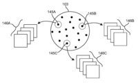
도 2는 후보 결함 및 선택된 후보 결함 또는 그 부근에서 수집된 이미지를 포함하는 웨이퍼를 예시하는 도면이다.
도 3은 특정한 측정 애플리케이션에 대한 결함을 분류하도록 구성된 시스템의 일 실시예의 단순화된 개략도이다.
도 4는 일 실시예에서 결함 분류기 트레이닝 엔진을 예시하는 도면이다.
도 5는 결함 분류에 유용한 결함 이미지의 속성을 식별하기 위해 사용되는 신경망 모델의 단순화된 예시를 도시한다.
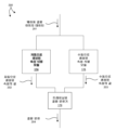
도 6은 트레이닝된 신경망 모델의 계층을 에뮬레이트하도록 트레이닝된 통계적 분류기의 단순화된 예시를 도시한다.
도 7은 일 실시예에서 결함 분류 엔진(200)의 예시를 도시한다.
도 8은 상이한 분류기에 기초하는 공지된 분류의 결함과 연관된 포착 레이트 대(versus) 뉴슨스 레이트의 플롯을 도시한다.
도 9는 통계적 분류기에 의해 측정된 상대적 중요도에 기초하여 랭크된(ranked) 속성의 목록을 예시하는 차트를 도시한다.
도 10은 웨이퍼 생산 프로세스의 질화규소 제거 단계에서 3D NAND 구조(180)의 단순화된 예시를 도시한다.
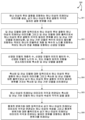
도 11은 결함 이미지의 자동으로 생성된 속성에 기초하여 결함을 분류하는데 유용한 예시적인 방법(300)의 흐름도를 도시한다.1 is a simplified schematic diagram of one embodiment of an
2 is a diagram illustrating a wafer containing candidate defects and images collected at or near selected candidate defects.
3 is a simplified schematic diagram of one embodiment of a system configured to classify defects for a particular measurement application.
4 is a diagram illustrating a defect classifier training engine in one embodiment.
5 shows a simplified example of a neural network model used to identify attributes of a defect image that are useful for defect classification.
6 shows a simplified example of a statistical classifier trained to emulate a layer of a trained neural network model.
7 shows an example of a
8 shows a plot of the acquisition rate versus the Newson's rate associated with known classifications of defects based on different classifiers.
9 shows a chart illustrating a list of attributes ranked based on their relative importance as measured by a statistical classifier.
10 shows a simplified illustration of a
11 shows a flow diagram of an
이제 본 발명의 배경 예 및 일부 실시예가 상세하게 참조될 것이며, 그 예는 첨부 도면에 도시되어 있다. Reference will now be made in detail to a background example and some embodiments of the present invention, examples of which are shown in the accompanying drawings.
반도체 구조 내에서 관심 결함(DOI)의 개선된 검출 및 분류를 위한 방법 및 시스템이 본 명세서에서 설명된다. 특히, 광학 검사를 기반으로 하는 뉴슨스 필터링 및 결함 분류는, 후보 결함의 이미지로부터 유도된 하나 이상의 자동으로 생성된 속성의 값을 추정함으로써 실현된다. 통계적 분류기는 자동으로 생성된 속성의 값에 기초하여 결함을 분류하도록 트레이닝된다.Methods and systems for improved detection and classification of defects of interest (DOIs) within semiconductor structures are described herein. In particular, Newsonian filtering and defect classification based on optical inspection is realized by estimating the values of one or more automatically generated attributes derived from images of candidate defects. Statistical classifiers are trained to classify defects based on automatically generated values of attributes.
자동으로 생성된 속성은, 딥 러닝 모델을 반복적으로 트레이닝, 축소, 및 리트레이닝하여 결정된다. 딥 러닝 모델은 후보 결함의 광학 이미지를 해당 결함의 알려진 분류와 관련시킨다. 딥 러닝 모델은 반복적으로 복잡성을 줄이면서 충분한 분류 성능을 유지한다. 모델 축소 후, 후보 결함의 광학 이미지를 알려진 결함 분류와 강하게 연관시키는 축소된 모델의 속성이 식별된다. 축소된 모델은 후속적으로, 알려지지 않은 분류를 갖는 후보 결함의 이미지와 연관되는 식별된 속성의 값을 생성하는데 사용된다. 속성 값은 후보 결함을 분류하기 위해 통계적 분류기에 의해 사용된다.The automatically generated attributes are determined by iteratively training, reducing, and retraining the deep learning model. A deep learning model relates an optical image of a candidate defect to a known class of that defect. Deep learning models maintain sufficient classification performance while iteratively reducing complexity. After model reduction, attributes of the reduced model that strongly associate the optical image of a candidate defect with a known defect class are identified. The reduced model is subsequently used to generate values of identified attributes that are associated with images of candidate defects with unknown classifications. Attribute values are used by statistical classifiers to classify candidate defects.
이러한 방식으로, 결함의 인라인 분류는, 검출된 이미지에 대해 작동하는 계산 비용이 많이 들고 복잡한 신경망이 아니라 계산 비용이 저렴한 통계적 분류기에 의해 수행된다. 계산 비용이 많이 드는 딥 러닝은, 트레이닝 단계에서만 사용되지만 인라인 검사 중에는 사용되지 않는다. 트레이닝된 딥 러닝 기반 모델은, 과도한 파라미터화 및 네트워크 용량을 최소화하기 위해 축소되며, 그 후, 축소된 네트워크는 웨이퍼 스캔 동안에 계산 효율적인 속성 계산에 사용된다.In this way, inline classification of defects is performed by a computationally inexpensive statistical classifier rather than by a computationally expensive and complex neural network operating on the detected image. Deep learning, which is computationally expensive, is only used during the training phase, but not during inline inspection. The trained deep learning-based model is reduced to minimize excessive parameterization and network capacity, and then the reduced network is used for computationally efficient attribute calculations during wafer scans.
딥 러닝에 기초하여 식별된 속성을 기반으로 결함 분류를 수행하면 특정 사용 사례에 맞는 속성을 학습할 수 있다. 일반적으로, 원하는 분류 작업은, 딥 러닝 기반 모델의 트레이닝 중에 사용되는 출력 및 목적 함수의 선택을 안내한다. 이러한 방식으로, 동일한 데이터를 사용하여, 출력 및 목적 함수의 선택을 기반으로 하는 특정 분류 작업에 각각 최적으로 적합한 상이한 속성을 학습한다. 일부 예에서, 하나의 결함 유형을 다른 결함 유형과 가장 잘 분리하는 속성이 학습된다(즉, 결함 분류). 이들 예에서, 출력은 각각 다른 결함 클래스이고, 목적 함수는 각 후보 결함에 대한 결함 클래스 중 하나의 클래스로부터 이진 선택을 강제한다. 일부 예에서, 관심 결함(DOI), 즉, 뉴슨스 필터링으로부터 뉴슨스 결함을 가장 잘 분리하는 다른 속성이 학습된다. 이들 예에서, 출력은 DOI 또는 뉴슨스 결함이고, 목적 함수는 각 후보 결함에 대해 이들 2개의 결함 클래스 중 하나의 클래스의 이진 선택을 강제한다.Performing fault classification based on properties identified based on deep learning allows learning properties specific to specific use cases. In general, the desired classification task guides the selection of output and objective functions used during training of a deep learning-based model. In this way, using the same data, different properties are learned, each optimally suited to a particular classification task based on the choice of output and objective function. In some examples, the attribute that best separates one defect type from another is learned (ie, a defect classification). In these examples, the outputs are each a different defect class, and the objective function forces a binary selection from one of the defect classes for each candidate defect. In some examples, another property that best separates a defect of interest (DOI), i.e., a Newsonian defect from a Newsonian filtering, is learned. In these examples, the output is a DOI or Newson's defect, and the objective function forces a binary selection of one of these two defect classes for each candidate defect.
도 1은 후보 결함을 검출하고 반도체 구조의 관심 결함(DOI)을 분류하도록 구성된 광학 검사 시스템(100)의 일 실시예의 단순화된 개략도이다. 광학 검사 시스템(100)은, 컴퓨팅 시스템, 웨이퍼 위치결정 시스템, 그리고 조명 서브시스템, 수집 서브시스템, 및 하나 이상의 검출기를 포함하는 광학 검사 서브시스템을 포함한다. 조명 서브시스템은 조명 소스(101) 및 조명 소스로부터 웨이퍼까지의 조명 광학 경로의 모든 광학 요소를 포함한다. 수집 서브시스템은 시료에서 각 검출기까지의 수집 광학 경로의 모든 광학 요소를 포함한다. 단순화를 위해, 시스템의 일부 광학 구성요소가 생략되어 있다. 예를 들어, 접는 거울, 편광기, 빔 형성 광학계, 추가 광원, 추가 수집기 및 검출기가 포함될 수도 있다. 이러한 모든 변형은 본 명세서에 설명된 본 발명의 범위 내에 있다. 본 명세서에 설명된 검사 시스템은 패턴화된 웨이퍼 및 패턴화되지 않은 웨이퍼 및 레티클을 검사하는데 사용될 수 있다.1 is a simplified schematic diagram of one embodiment of an
도 1에 도시된 바와 같이, 웨이퍼(103)는 하나 이상의 조명 소스(101)에 의해 생성된 수직 입사 빔(104)에 의해 조명된다. 대안적으로, 조명 서브시스템은 경사 입사각으로 시료에 광선을 지향시키도록 구성될 수 있다. 일부 실시예에서, 시스템(100)은 경사 입사광 빔 및 수직 입사광 빔과 같은 다수의 광 빔을 시료에 지향시키도록 구성될 수 있다. 복수의 광빔은 실질적으로 동시에 또는 순차적으로 시료로 지향될 수 있다.As shown in FIG. 1 ,
조명 소스(101)는 예를 들어, 광대역 레이저 지속 플라즈마 광원, 레이저, 초연속체 레이저, 다이오드 레이저, 헬륨 네온 레이저, 아르곤 레이저, 고체 상태 레이저, DPSS(diode pumped solid state) 레이저, 크세논 아크 램프, 가스 방전 램프, LED 어레이 및 백열 램프를 포함할 수 있다. 광원은 거의 단색광 또는 광대역 광을 방출하도록 구성될 수 있다. 일부 실시예에서, 조명 서브시스템은 또한, 시료로 향하는 광의 파장을 제한할 수 있는 하나 이상의 스펙트럼 필터를 포함할 수 있다. 하나 이상의 스펙트럼 필터는 대역통과 필터 및/또는 에지 필터 및/또는 노치 필터일 수 있다. 조명은 임의의 적절한 파장 범위에 걸쳐 시료에 제공될 수 있다. 일부 예에서, 조명 광은 260 나노미터 내지 950 나노미터 범위의 파장을 포함한다. 일부 예에서, 조명 광은 높은 종횡비 구조의 결함을 포착하기 위해 950 나노미터보다 큰 파장(예를 들어, 2,500 나노미터 및 그 이상으로 확장)을 포함한다. 일부 실시예에서, 조명 서브시스템은 또한 시료로 향하는 조명 광의 편광을 제어하기 위해 하나 이상의 편광 광학계를 포함할 수 있다.The
조명 소스(101)에 의해 생성된 빔(104)은, 빔 스플리터(105)로 지향된다. 빔 스플리터(105)는 빔을 대물 렌즈(109)로 향하게 한다. 대물 렌즈(109)는 입사 스폿(spot)(119)에서 웨이퍼(103) 상으로 빔(111)을 포커싱한다. 입사 스폿(119)은 조명 소스(101)로부터 웨이퍼(103)의 표면 상으로 방출된 광의 투영에 의해 규정된다(즉, 형상 및 크기가 정해짐).The
검사 시스템(100)은 조명 개구(124)를 포함한다. 도 1에 도시된 바와 같이, 컴퓨팅 시스템(130)은 명령 신호(122C)를 조명 개구(124)에 전달한다. 이에 응답하여, 조명 개구(124)는 웨이퍼(103)의 표면 상에 제공된 조명 방향 및 빔 형상을 조정한다. 일 실시예에서, 조명 개구(124)는 컴퓨팅 시스템(130)으로부터 전달된 명령 신호(122C)에 의해 제어되는 다양한 개구 형상을 제공하는 어셈블리이다.The
도 1에 도시된 바와 같이, 컴퓨팅 시스템(130)은 명령 신호(122A)를 조명 소스(101)에 전달한다. 이에 응답하여, 조명 소스(101)는 조명 빔(111)의 스펙트럼 범위(들)를 조정한다. 일반적으로, 웨이퍼(103)에 입사하는 빔(111)은, 편광, 강도, 크기 및 모양 등을 포함하여 하나 이상의 방식으로 조명 소스(101)에 의해 방출된 광과 다를 수 있다.As shown in FIG. 1 ,
도 1에 도시된 실시예에서, 검사 시스템(100)은 선택 가능한 조명 편광 요소(147)를 포함한다. 일 예에서, 컴퓨팅 시스템(130)은 명령 신호(122E)를 조명 편광 요소(147)에 전달한다. 이에 응답하여, 조명 편광 요소(147)는 웨이퍼(103)의 표면 상에 제공된 조명 광의 편광을 조정한다.In the embodiment shown in FIG. 1 ,
도 1에 도시된 바와 같이, 검사 시스템(100)은 웨이퍼(103)에 전달되는 조명 전력을 제어하는 조명 전력 감쇠기(102)를 포함한다. 일부 다른 실시예에서, 조명 전력 밀도 감쇠기는, 웨이퍼(103)에 전달되는 조명 전력 밀도를 감소시키기 위해 조명 스폿(119)의 크기를 조절하는 빔 성형 요소이다. 일부 다른 실시예에서, 조명 전력 감소 및 빔 사이징(sizing)의 조합이 웨이퍼(103)에 전달되는 조명 전력 밀도를 감소시키기 위해 사용된다. 도 1에 도시된 바와 같이, 컴퓨팅 시스템(130)은 검출기(115, 120, 125) 중 임의의 검출기에 의해 검출된 이미지에 기초하여 조명 전력을 제어하기 위해 제어 신호(122B)를 조명 전력 감쇠기(102)에 전달한다. 일반적으로, 조명 전력 감쇠기(102)는 선택적이다. 따라서, 일부 다른 실시예에서, 검사 시스템(100)은 조명 전력 감쇠기(102)를 포함하지 않는다.As shown in FIG. 1 , the
일부 실시예에서, 시스템(100)은 조명 경로에 디플렉터(미도시)를 포함할 수 있다. 일 실시예에서, 디플렉터는 음향 광학 디플렉터(AOD)일 수 있다. 다른 실시예에서, 디플렉터는 기계적 스캐닝 어셈블리, 전자 스캐너, 회전 거울, 다각형 기반 스캐너, 공진 스캐너, 압전 스캐너, 갈보(galvo) 미러, 또는 검류계를 포함할 수 있다. 디플렉터는 시료 위의 광선을 스캔한다. 일부 실시예에서, 디플렉터는 대략 일정한 스캐닝 속도로 시료 위의 광선을 스캔할 수 있다.In some embodiments,
시스템(100)은 웨이퍼(103)에 의해 산란 및/또는 반사된 광을 수집하고 그 광을 검출기 어레이(115, 120, 125)에 각각 포커싱하기 위한 수집 광학계(116, 117, 및 118)를 포함한다. 검출기(115, 120, 및 125)의 출력은 신호를 처리하고 후보 결함의 존재 및 그 위치를 결정하기 위해 컴퓨팅 시스템(130)에 전달된다.
수집 광학계(116-118) 중 임의의 것은, 렌즈, 복합 렌즈, 또는 당해 분야에 공지된 임의의 적절한 렌즈일 수 있다. 대안적으로, 수집 광학계(116-118) 중 임의의 것은, 거울과 같은 반사형 또는 부분 반사형 광학 구성요소일 수 있다. 또한, 특정 수집 각도가 도 1에 도시되어 있지만, 수집 광학계는 임의의 적절한 수집 각도로 배열될 수 있음을 이해해야 한다. 수집 각도는 예를 들어, 입사각 및/또는 시료의 지형적 특성에 따라 변할 수 있다.Any of collection optics 116-118 may be lenses, compound lenses, or any suitable lenses known in the art. Alternatively, any of collection optics 116-118 may be reflective or partially reflective optical components, such as mirrors. Also, while a specific collection angle is shown in FIG. 1 , it should be understood that the collection optics may be arranged at any suitable collection angle. The collection angle may vary, for example, depending on the angle of incidence and/or topographical characteristics of the sample.
검출기(115, 120, 및 125)의 각각은 일반적으로 반사 및 산란된 광을 전기 신호로 변환하는 기능을 하며, 따라서 실질적으로 당업 분야에 공지된 임의의 광검출기를 포함할 수 있다. 그러나, 특정 검출기는 검출기의 원하는 성능 특성, 검사될 시료의 유형, 및 조명의 구성에 기초하여 본 발명의 하나 이상의 실시예 내에서 사용하기 위해 선택될 수 있다. 예를 들어, 검사에 사용할 수 있는 광의 양이 상대적으로 적은 경우, TDI(Time Delay Integration) 카메라와 같은 효율성 향상 검출기는 시스템의 신호 대 잡음비와 처리량을 증가시킬 수 있다. 그러나, 검사에 사용할 수 있는 광의 양과 수행되는 검사 유형에 따라, 전하 결합 소자(charge-coupled device; CCD) 카메라, 광다이오드, 광전관 및 광전자 증배관(PMT)과 같은 다른 검출기를 사용할 수 있다. 본 발명의 적어도 하나의 실시예에서, 광전자 증배관은 시료로부터 산란된 광을 검출하기 위해 사용된다. 각 검출기는 하나의 감지 영역만 포함하거나 가능하게는 여러 감지 영역(예를 들어, 검출기 어레이 또는 다중 양극 PMT)을 포함할 수 있다.Each of
시스템(100)은 명시야 및 암시야 모드와 같은 다양한 이미징 모드를 사용할 수 있다. 예를 들어, 일 실시예에서, 검출기(125)는 명시야 이미지를 생성한다. 도 1에 도시된 바와 같이, 웨이퍼(103)의 표면으로부터 좁은 각도로 산란된 광량의 일부는 대물 렌즈(109)에 의해 집광된다. 이 광은 대물 렌즈(109)를 다시 통과하여 빔 스플리터(105)에 충돌한다. 빔 스플리터(105)는 광의 일부를 수집 광학계(118)로 전송하고, 수집 광학계는 차례로 검출기(125)에 광을 포커싱한다. 이러한 방식으로, 명시야 이미지는 검출기 어레이(125)에 의해 생성된다. 수집 광학계(118)는 대물 렌즈(109)에 의해 수집된 반사광을 검출기 어레이(125) 상으로 이미징하는 이미징 렌즈(107)를 포함한다. 조리개(182), 푸리에 필터(106), 또는 둘 다는 대물 렌즈(109)의 후면 초점면에 배치된다. 명시야, 암시야, 및 위상 콘트라스트와 같은 다양한 이미징 모드는, 다른 조명 개구(124), 수집 개수, 푸리에 필터(106), 또는 이들의 조합을 사용하여 구현될 수 있다. 조명 방향이나 이미징 수집 입체각과 같은 이미징 모드의 구성은, DOI 신호 및 수집된 이미지에 기초하여 결정될 수 있다. 본 명세서에 참고로 통합되는 미국 특허 제7,295,303호 및 제7,130,039호는 이들 이미징 모드를 더욱 상세하게 설명한다. 다른 예에서, 검출기(115 및 120)는 더 큰 시야각에서 수집된 산란광을 이미징함으로써 암시야 이미지를 생성한다. 본 명세서에 참고로 통합된 미국 특허 제6,208,411호는 이러한 이미징 모드를 더욱 상세하게 설명한다.
도 1에 도시된 실시예에서, 검사 시스템(100)은 선택 가능한 수집 편광 요소(181)를 포함한다. 일 예에서, 컴퓨팅 시스템(130)은 명령 신호(122F)를 수집 편광 요소(181)에 전달한다. 이에 응답하여, 수집 편광 요소(181)는 검출기(125)의 표면 상에 제공되는 수집된 광의 편광을 조정한다.In the embodiment shown in FIG. 1 ,
도 1에 도시된 바와 같이, 검사 시스템(100)은 선택 가능한 푸리에 필터(106)를 포함한다. 컴퓨팅 시스템(130)은 명령 신호(122D)를 푸리에 필터(106)에 전달한다. 이에 응답하여, 푸리에 필터(106)는 (예를 들어, 수집 빔 경로에 위치한 특정 푸리에 필터 요소를 변경함으로써) 푸리에 필터의 푸리에 필터링 특성을 조정한다.As shown in FIG. 1 ,
검사 시스템(100)은 수집 개구(182)를 포함한다. 도 1에 도시된 바와 같이, 컴퓨팅 시스템(130)은 명령 신호(122G)를 수집 개구(182)에 전달한다. 이에 응답하여, 수집 개구(182)는, 대응하는 검출기로 전송되는, 웨이퍼(103)의 표면으로부터 수집된 광의 양을 조정한다. 일 실시예에서, 수집 개구(182)는 컴퓨팅 시스템(130)으로부터 전달된 명령 신호(122G)에 의해 제어되는 다양한 개구 형상을 제공하는 어셈블리이다.The
시스템(100)은 또한 검출기(115, 120, 및 125) 중 임의의 검출기에 의해 검출된 반사 및/또는 산란 신호를 처리하는데 필요한 다양한 전자 구성요소(도시되지 않음)를 포함한다. 예를 들어, 시스템(100)은, 검출기(115, 120, 및 125) 중 임의의 검출기로부터 출력 신호를 수신하고 이러한 출력 신호를 미리 결정된 양만큼 증폭하는 증폭기 회로 및 증폭된 신호를 프로세서(131) 내에서 사용하기에 적합한 디지털 포맷으로 변환하는 아날로그/디지털 변환기(ADC)를 포함할 수 있다. 일 실시예에서, 프로세서는 전송 매체에 의해 ADC에 직접 결합될 수 있다. 대안적으로, 프로세서는 ADC에 결합된 다른 전자 구성요소로부터 신호를 수신할 수 있다. 이러한 방식으로, 프로세서는 전송 매체 및 임의의 개재 전자 구성요소에 의해 ADC에 간접적으로 결합될 수 있다.
도 1에 도시된 실시예에서, 웨이퍼 위치결정 시스템(114)은, 컴퓨팅 시스템(130)으로부터 수신된 명령(126)에 기초하여 빔(111) 아래에서 웨이퍼(103)를 이동시킨다. 웨이퍼 위치결정 시스템(114)은 웨이퍼 척(108), 움직임 제어기(113), 회전 스테이지(110), 병진 이동 스테이지(112), 및 z-병진 이동 스테이지(121)를 포함한다. Z-병진 이동 스테이지(121)는 웨이퍼(103)의 표면에 수직인 방향(예를 들어, 좌표계(123)의 z-방향)으로 웨이퍼(103)를 이동시키도록 구성된다. 병진 이동 스테이지(112) 및 회전 스테이지(110)는 웨이퍼(103)의 표면에 평행한 방향(예를 들어, 좌표계(123)의 x 및 y 방향)으로 웨이퍼(103)를 이동시키도록 구성된다. 일부 다른 실시예에서, 웨이퍼(103)는 다중 병진 이동 스테이지의 조정된 움직임에 의해 면내 방향(예를 들어, x 및 y 방향)으로 이동된다.In the embodiment shown in FIG. 1 ,
웨이퍼(103)는, 웨이퍼 척(108) 상에 지지된다. 일부 실시예에서, 웨이퍼(103)는 회전 스테이지(110)의 회전 축과 대략 정렬된 기하학적 중심에 위치된다. 이러한 방식으로, 회전 스테이지(110)는 허용 가능한 허용 오차 내에서, 지정된 각속도(ω)로 기하학적 중심을 중심으로 웨이퍼(103)를 회전시킨다. 또한, 병진 이동 스테이지(112)는, 지정된 속도(VT)로 회전 스테이지(110)의 회전 축에 대략 수직인 방향으로 웨이퍼(103)를 병진 이동시킨다. 움직임 제어기(113)는, 검사 시스템(100) 내에서 웨이퍼(103)의 원하는 면내 스캐닝 움직임을 달성하기 위해 회전 스테이지(110)에 의한 웨이퍼(103)의 회전 및 병진 이동 스테이지(112)에 의한 웨이퍼(103)의 병진 이동을 조정한다. 또한, 움직임 제어기(113)는 검사 시스템(100) 내에서 웨이퍼(103)의 원하는 면외 스캐닝 움직임을 달성하기 위해 병진 이동 스테이지(121)에 의한 웨이퍼(103)의 이동을 조정한다. The
웨이퍼(103)는 복수의 상이한 모드에서 검사 시스템(100)의 광학 서브시스템에 대해 위치될 수 있다. 검사 모드에서, 웨이퍼(103)는 2차원 스캔을 위해 측방향(예를 들어, x 방향 및 y 방향)으로 반복적으로 스캔된다. 또한, 웨이퍼(103)는 3차원 스캔을 위해 상이한 z-위치에서 측방향으로 반복 스캔될 수 있다. 일부 예에서, 웨이퍼(103)는 적층 구조를 통해 2개 이상의 깊이(예를 들어, 웨이퍼 표면 아래의 거리)에 대응하는 2개 이상의 상이한 z-위치에서 스캔된다. 결함 검토 모드에서, 웨이퍼(103)는 z 방향으로 스캐닝하는 동안 x 방향 및 y 방향으로 고정된 위치에 위치된다. 이러한 방식으로, 측정 중인 구조체 내의 깊이 범위에 걸쳐 웨이퍼(103)의 고정된 측방 위치에서 측정 데이터에 기초하여 3차원 이미지가 생성된다. 결함 검토 모드는 일반적으로 결함에 대한 보다 상세한 조사(예를 들어, 더 높은 이미지 해상도, 더 높은 초점 깊이 해상도, 또는 둘 다)를 수행하는데 사용된다.
일부 실시예에서, 웨이퍼는 웨이퍼 스택의 상이한 깊이를 이미징하기 위해 검사 시스템의 초점면에 대해 복수의 상이한 z-위치로 이동된다. 일부 다른 실시예에서, 검사 시스템의 초점면의 위치는 웨이퍼 스택의 상이한 깊이를 이미징하기 위해 웨이퍼에 대해 복수의 상이한 z-위치로 광학적으로 조정된다. 일부 예에서, 각각의 z-위치에서 수집된 이미지는, 2개의 측방 치수(예를 들어, 웨이퍼 표면에 평행) 및 복수의 상이한 깊이(즉, 상이한 z-위치)에서 측정된 두꺼운 반도체 구조의 3차원 체적 이미지를 형성하기 위해 집계된다.In some embodiments, the wafer is moved to a plurality of different z-positions relative to the focal plane of the inspection system to image different depths of the wafer stack. In some other embodiments, the position of the focal plane of the inspection system is optically adjusted to a plurality of different z-positions relative to the wafer to image different depths of the wafer stack. In some examples, the images collected at each z-position are three lateral dimensions of the thick semiconductor structure measured in two lateral dimensions (eg, parallel to the wafer surface) and at a plurality of different depths (ie, different z-positions). are aggregated to form a dimensional volumetric image.
일반적으로, 조명 및 수집 서브시스템 둘 다를 포함하는 광학 서브시스템(140)은, 측정 중인 구조(예를 들어, 수직 적층 구조)의 복수의 상이한 깊이에 위치된 복수의 초점면의 각각에서 포커싱된 광학 이미지를 생성한다. 각각의 상이한 깊이에서 광학 서브시스템의 초점면의 정렬은, 초점면을 z 방향으로 이동시키는 광학 조정, z 방향으로의 시료 위치결정, 또는 둘 다에 의해 달성된다. 하나 이상의 검출기는, 복수의 상이한 깊이의 각각에서 수집된 광을 검출하고, 복수의 상이한 깊이의 각각에서 수집된 광의 양을 나타내는 복수의 출력 신호를 생성한다.
일부 예에서, 광학 검사 시스템(100)은 2개의 측방 치수(예를 들어, 웨이퍼 표면에 평행한 치수) 및 깊이 치수(예를 들어, 웨이퍼 표면에 수직인 치수)로 측정된 체적으로부터 두꺼운 반도체 구조의 3차원 이미지를 생성한다. 도 1에 도시된 실시예에서, 컴퓨팅 시스템(130)은 하나 이상의 측정 채널로부터(예를 들어, 하나 이상의 검출기(115, 120, 및 125)로부터)의 출력을, 측정된 체적에 대응하는 체적 데이터 세트로 배열한다. In some examples, the
결함 검토 예에서, 일련의 이미지가 검사 시스템의 초점면 내의 다수의 상이한 웨이퍼 위치에 대한 동일한 (x,y) 위치에서 획득된다. 이 예에서, 컴퓨팅 시스템(130)은 각각의 상이한 초점 오프셋에서 획득된 일련의 2차원 이미지의 스택을 어셈블링함으로써 측정된 체적의 3차원 이미지를 생성한다. 초점 오프셋은 시료의 가장 반사율이 높은 표면과 검사 시스템의 초점면 사이의 상대 거리이다. 일반적으로, 스캔할 파라미터는 초점 오프셋에 제한되지 않는다. 다른 예에서, 센서 축 위치, 스펙트럼 대역, 조명 방향 등이 스캔되어, 3차원 결함 이미지를 형성할 수 있다. 일부 실시예에서, 3차원보다 많은 치수를 갖는 결함 이미지가 컴퓨팅 시스템(130)에 의해 생성된다. 일 예에서, 초점 오프셋과 조명 방향 모두는 주어진 (x, y) 위치에 대해 스캔된다. 일 예에서, 컴퓨팅 시스템(130)은 각각의 상이한 초점 오프셋 및 각각의 상이한 조명 각도에서 획득된 일련의 2차원 이미지를 4차 텐서(tensor)로 어셈블링함으로써 측정된 체적의 4차원 이미지를 생성한다. 일부 예에서, 미리 정의된 초점 오프셋 세트에 대한 일련의 이미지는, 조명 강도 및 다른 시스템 파라미터를 변경하지 않고 유지하면서 수집된다.In the defect review example, a series of images are acquired at the same (x,y) location for a number of different wafer locations within the focal plane of the inspection system. In this example,
일반적으로, 결함 검출 알고리즘을 적용함으로써 이미지로부터 결함을 검출한다. 일부 실시예에서, 결함 검출은 검사 시스템(100)에 의해 생성된 이미지 데이터로부터 직접 수행된다. 일부 실시예에서, 수집된 이미지 데이터로부터 하나 이상의 속성 벡터가 추출되고, 측정된 속성 벡터에 기초하여 결함 검출이 수행된다. 일반적으로, 속성 벡터는 객체(object)(예: 관심 결함, 공칭 구조 등)를 나타내는 숫자 속성의 n차원 벡터이다. 일부 예에서, 결함 검출 알고리즘은 결함 검출 알고리즘의 감도를 조정하는 하나 이상의 선택 가능한 임계값을 포함한다. 매우 제한적인 임계값을 선택하면, 결함 검출 알고리즘이 이미지 세트에서 더 적은 수의 관심 결함을 검출한다. 높은 허용 임계값을 선택하면, 결함 검출 알고리즘이 동일한 이미지 세트에서 더 많은 관심 결함을 검출한다. 너무 적은 수의 결함이 검출되면 실제 결함을 놓칠 수 있고, 너무 많은 결함이 검출되면 많은 뉴슨스(예를 들어, 거짓(false)) 결함이 포착된다. 따라서, 특정 측정 애플리케이션에 맞게 조정된 최적화된 측정 레시피는, 실제 결함의 포착 레이트를 최대화하면서 뉴슨스(즉, 거짓) 결함의 포착 레이트를 최소화하는 검출 알고리즘 임계값을 선택하는 것을 포함한다.Generally, defects are detected from an image by applying a defect detection algorithm. In some embodiments, defect detection is performed directly from image data generated by
도 1에 대해 설명된 바와 같이, 컴퓨팅 시스템(130)은 조명 전력, 조명 개구, 수집 개수, 스펙트럼 대역, 푸리에 필터, 조명 편광, 수집 편광, 또는 이들의 임의의 조합이 지정된 광학 모드에 따라 선택되도록, 명령 신호(122A-G)를 생성하고 전달한다. 또한, 검사 시스템(100)과 같은 검사 시스템은, 입사각, 방위각 등과 같은 다른 선택 가능한 광학 시스템 설정을 포함한다. 광학 시스템 설정의 각각의 별개의 조합은 광학 검사 시스템(100)의 별개의 광학 모드로 지칭된다.As described with respect to FIG. 1 ,
실제로, 하나 이상의 성능 목표를 달성하기 위해 특정 측정 애플리케이션에 대해 최적의 광학 모드가 선택된다. 예시적인 성능 목표는 검출된 이미지에서 공칭 구조의 응답을 최소화하는 것, 검출된 이미지에서 결함 신호의 응답을 향상시키는 것, 검출된 이미지에서 웨이퍼 노이즈 또는 뉴슨스 신호의 응답을 최소화하는 것, 웨이퍼 노이즈 또는 검출된 이미지의 뉴슨스 신호로부터의 결함의 응답을 구별하는 것, 검출된 이미지로부터 결함의 추정된 물리적 위치의 정확도를 개선하는 것, 또는 이들의 임의의 조합을 포함하지만, 이에 제한되지는 않는다.In practice, the optimal optical mode is selected for a particular measurement application to achieve one or more performance goals. Exemplary performance goals include minimizing the response of the nominal structure in the detected image, improving the response of the defect signal in the detected image, minimizing the response of wafer noise or Newson's signal in the detected image, wafer noise or differentiating the response of a defect from a Newson's signal of a detected image, improving the accuracy of an estimated physical location of a defect from a detected image, or any combination thereof. .
도 1에 도시된 실시예에서, 고려 중인 측정 애플리케이션(136)에 대한 정보는 사용자 입력 소스(135)로부터 컴퓨팅 시스템(130)에 의해 수신된다. 일반적으로, 사용자 입력 소스(135)는 검사 중인 구조 및 예상되는 결함에 대한 지식을 가진 사용자 또는 조작자와 같은 엔티티이다. 비제한적인 예로서, 구조적 정보(136)는 관심 결함의 예상 스택 깊이, 관심 결함의 웨이퍼 레벨 시그니처, 3-D 스택의 굴절률 등을 포함한다. 일 실시예에서, 검사 시스템(100)은 사용자로부터 검사 시스템(100)으로 구조적 정보(136)를 전달하기 위해 조작자(예를 들어, 키보드, 마우스, 터치스크린, 통신 포트 등)로부터 입력을 수용하는데 유용한 주변 장치를 포함한다.In the embodiment shown in FIG. 1 , information about the
일부 실시예에서, 사용자는 또한 검사 시스템(100)에 대한 광학 모드의 초기 세트를 전달한다. 검사 시스템(100)의 사용자는 일반적으로 예비 모델링을 수행하거나 과거 경험을 사용하여, 검사 시스템(100)의 광학 모드의 초기 세트에 도달하는데, 이는 최상의 검사 결과를 초래할 가능성이 가장 높다. 일반적으로, 초기 광학 모드 세트는 수십 개의 상이한 광학 모드를 포함하지만, 수천 개의 사용 가능한 광학 모드보다 훨씬 적다. 일부 예에서, 사용자는 또한 하나 이상의 초기 초점 레벨을 검사 시스템(100)에 전달한다. 하나 이상의 초기 초점 레벨은 관심 결함이 위치해야 하는 초점 레벨을 포함한다.In some embodiments, the user also conveys an initial set of optical modes for
사용자 입력(136 및 137)에 응답하여, 검사 시스템(100)은 광학 모드의 초기 세트의 각각에서 그리고 하나 이상의 초기 초점 레벨의 각각에서 웨이퍼(103)의 검사를 수행한다. 일반적으로, 검사는 웨이퍼의 넓은 영역(예를 들어, 웨이퍼의 전체 영역)이 하나 이상의 초기 초점 레벨의 각각에서 검사되는 스캐닝 모드에서 실행된다. 초기 검사 동안에 사용된 결함 검출 알고리즘의 임계값은, 많은 후보 결함(즉, 실제 결함과 뉴슨스 결함 모두)을 식별하는 높은 허용 값으로 설정된다. 예를 들어, 도 2는 웨이퍼(103) 상의 검사 시스템(100)에 의해 식별된 후보 결함을 도시한다.In response to
초기 검사를 수행한 후, 컴퓨팅 시스템(130)은 초기 검사에서 식별된 가장 유망한 후보 결함(예를 들어, 도 2에 도시된 후보 결함(145A-C)) 중 몇 가지를 선택한다. 가장 유망한 결함은, 검사 시스템(100)의 사용자에 의해 제공되는 예상 결함과 가장 근접하게 일치하는 관심 결함이다.After performing the initial tests,
일부 실시예에서, 검사 시스템(100)은 선택된 관심 결함이 검사 시스템(100)의 시야 내에 있도록, 광학 검사 서브시스템(140)에 대해 웨이퍼(103)의 위치를 결정함으로써 선택된 관심 결함의 스루(through) 초점 검토를 수행한다. 측정 중인 구조 전체에 걸쳐 복수의 초점 레벨에서 일련의 측정이 수행된다. 스루 초점 검토의 결과에 기초하여, 컴퓨팅 시스템(130)은 관심 결함을 가장 잘 포착하는 하나 이상의 초점면 또는 초점 범위를 결정한다. 일부 예에서, 하나 이상의 초점면 또는 초점 범위는, 측정된 결함 시그니처(예를 들어, 이미지 또는 속성 벡터)와 예상된 결함 시그니처 간의 최상의 매치에 기초하여 결정된다.In some embodiments, the
하나 이상의 초점면 또는 초점 범위를 결정한 후, 검사 시스템(100)은, 구조체의 전체 깊이 전체에 대한 것이기 보다는, 초기 검사의 각각에서 하나 이상의 초점면 또는 초점 범위에서 식별된 결함 위치와 연관된 이미지 패치(예를 들어, 32x32 픽셀 패치, 64x64 픽셀 패치 등)를 기록한다. 도 2는 각각 후보 결함(145A-C)과 연관된 이미지 패치(146A-C)의 세트를 도시한다. 일부 예에서, 1억 개 이상의 결함 위치가, 다중 초점 레벨에서 이미징되고 기록된다. 이러한 방식으로, 결함 발견과 연관되는 기록된 데이터의 양은 깊이의 서브세트로 제한된다. 기록된 데이터는 후속 결함 검증 및 분류기 트레이닝 프로세스 동안에 사용된다. 기록된 데이터의 양을 제한함으로써, 후속 결함 검증 및 분류기 트레이닝 프로세스가 크게 간소화된다.After determining one or more focal planes or focal ranges,
다른 양태에서, 검증된 결함 이미지 및 연관된 결함 분류는 검사 시스템(100)에 의해 식별된 대응하는 결함에 매핑된다. 연관된 기록 이미지 및 결함 분류를 포함하는 검증된 결함은, 뉴슨스 필터, 통계적 분류기, 또는 둘 다를 트레이닝하는데 사용된다.In another aspect, the verified defect images and associated defect classifications are mapped to corresponding defects identified by
도 3은 반도체 구조의 검사를 위한 결함 발견 및 검증을 위한 시스템(150)의 일 실시예의 단순화된 개략도이다. 시스템(150)은 도 1을 참조하여 설명된 검사 시스템(100), 결함 검증 툴(151), 및 컴퓨팅 시스템(160)을 포함한다. 일부 실시예에서, 컴퓨팅 시스템(160)에 의해 수행되는 작업은 본 명세서에 설명된 바와 같이 컴퓨팅 시스템(130) 또는 또 다른 컴퓨팅 시스템에 의해 구현된다. 3 is a simplified schematic diagram of one embodiment of a
일부 실시예에서, 결함 검증 툴(151)은 전자 빔 기반 분석 툴이다. 일부 다른 실시예에서, 결함 검증 툴(151)은 x-선 기반 분석 툴이다. 이들 실시예에서, 매립된 결함을 x-선 기반 분석 툴에 가시적으로 만들기 위해 재료 제거 툴이 필요하지 않을 수 있다. 따라서, 관련 재료 제거 툴은 옵션이다.In some embodiments, defect verification tool 151 is an electron beam based analysis tool. In some other embodiments, defect verification tool 151 is an x-ray based analysis tool. In these embodiments, a material removal tool may not be needed to make the buried defect visible to an x-ray based analysis tool. Therefore, a related material removal tool is optional.
일부 예에서, 결함 검증은 웨이퍼(103)를 디프로세싱하고 검사 시스템(100)을 사용하여 노출된 결함을 검사함으로써 달성된다. 이들 예에서, 다른 결함 검증 툴(151)은 필요하지 않을 수 있다. 일부 실시예에서, SEM 검토 툴과 같은 결함 검증 툴은, 단일 웨이퍼 처리 툴로서 검사 시스템(100)과 통합될 수 있거나, 대안적으로는, 개별적으로 또는 임의의 조합으로 상이한 웨이퍼 처리 시스템으로 분리될 수 있다. In some examples, defect verification is accomplished by deprocessing the
컴퓨팅 시스템(130)은 검사 프로세스를 조정하고, 분석, 데이터 처리, 및 통신 작업을 수행한다. 이와 유사하게, 컴퓨팅 시스템(160)은 물질 제거 및 검토 프로세스를 조정하고, 분석을 수행하고, 데이터 처리 및 통신 작업을 수행한다.
결함 검증은 많은 상이한 방식으로 달성될 수 있다. 일부 실시예에서, 결함을 검증하기 위해 전압 콘트라스트 검사가 수행된다. 이들 실시예에서, 웨이퍼는 작은 샘플 계획에 따라 장식되고, 전압 콘트라스트 측정은 전압 콘트라스트 검사 툴에 의해 상기 장식된 웨이퍼에 대해 수행된다.Fault verification can be accomplished in many different ways. In some embodiments, a voltage contrast check is performed to verify defects. In these embodiments, a wafer is decorated according to a small sample plan, and voltage contrast measurements are performed on the decorated wafer by a voltage contrast inspection tool.
일부 다른 실시예에서, 웨이퍼 제조가 완료되고 결함을 검증하기 위해 완성된 웨이퍼에 대해 비트맵 테스트가 수행된다.In some other embodiments, wafer fabrication is complete and bitmap testing is performed on the finished wafer to verify defects.
일부 다른 실시예에서, 웨이퍼는 고려 중인 다층 구조의 계층을 제거하기 위해 디프로세싱된다. 디프로세싱은 화학적 프로세스, 기계적 프로세스, 또는 둘 다에 의해 달성될 수 있다. 일 예로, FIB(focused ion beam; 포커싱된 이온 빔) 툴을 사용하여 웨이퍼의 표면으로부터 재료를 제거한다. 웨이퍼는 매립된 결함이 웨이퍼의 표면에 또는 그 근처에 위치될 때까지 디프로세싱되고, 결함 검증 툴(151), 예를 들어 SEM 검토 툴, 검사 시스템(100) 등에 의해 효과적으로 이미징될 수 있다. 결함 검증 측정과 연관되는 결함 위치 및 연관된 결함 이미지(152)는 메모리(예를 들어, 보드 컴퓨팅 시스템(160) 상의 메모리(162))에 저장된다. 일부 실시예에서, 결함 정보는 KLA 결과 파일(KLARF)의 형태로 저장된다. KLARF 파일은 결함 검증 툴(150)에 의해 생성된 플랫 ASCII 파일이다. 동일한 KLARF 파일 포맷은 검사 시스템(100)으로부터의 결함 정보를 저장하는데 사용된다.In some other embodiments, the wafer is deprocessed to remove layers of the multilayer structure under consideration. Deprocessing can be accomplished by chemical processes, mechanical processes, or both. In one example, a focused ion beam (FIB) tool is used to remove material from the surface of the wafer. The wafer is deprocessed until buried defects are located at or near the surface of the wafer, and can be effectively imaged by a defect verification tool 151, such as a SEM review tool,
추가 양태에서, 결함 발견의 일부로서 검사 시스템(100)에 의해 식별된 결함과 연관된 결함 정보(141)는, 컴퓨팅 시스템(160)에 전달된다. 컴퓨팅 시스템(160)은 식별된 결함을 샘플링하여 결함 검증 툴(151)로 전달되는 후보 결함(153)의 다양성 세트를 생성한다. 일부 실시예에서, 컴퓨팅 시스템(160)은 결함 발견 동안 검사 시스템(100)에 의해 식별된 결함(예를 들어, 1억 개 이상의 DOI)을 비닝(bin)하고, 후보 결함(153)의 다양성 세트를 생성하기 위해 각 빈(bin)으로부터 몇 개의 결함을 선택한다. 후보 결함(153)의 다양성 세트는, 메모리(예를 들어, 보드 컴퓨팅 시스템(160) 상의 메모리(162))에 저장된다.In a further aspect,
결함 검증 측정은 후보 결함의 다양성 세트에 대해 수행된다. 결함 검증 측정으로부터의 결함 위치, 결함 분류, 및 연관된 결함 이미지는, 메모리(예를 들어, 보드 컴퓨팅 시스템(160) 상의 메모리(162))에 저장된다. 결함 분류는 인간 사용자의 도움으로 또는 자동으로 수행될 수 있다. 결함 분류는 결함을 뉴슨스 결함 또는 관심 결함(DOI)으로서 식별한다. 결함이 DOI로서 분류되면, 결함의 특정 분류가 식별된다. 일부 실시예에서, 후보 결함의 다양성 세트와 연관되는 결함 위치, 분류, 및 연관된 결함 이미지는 또한, KLARF 파일 포맷으로 저장된다.Defect validation measurements are performed on a diverse set of candidate defects. The defect location, defect classification, and associated defect images from the defect verification measurements are stored in memory (eg,
후보 결함의 다양성 세트, 검증된 결함의 임의의 다른 세트, 또는 이들의 조합으로부터의 결함 검증 데이터는, 라벨링된 결함 데이터(171)로서 저장된 결함 이미지 패치에 매핑된다. 결함 검증 데이터 및 대응하는 결함 이미지 패치는, 뉴슨스 필터, 결함 분류기, 또는 둘 다를 트레이닝하는데 사용된다.The defect verification data from the diversity set of candidate defects, any other set of verified defects, or combinations thereof are mapped to defect image patches stored as labeled
일 양태에서, 통계적 분류기는 속성 식별 모듈에 의해 결함 이미지로부터 결정된 자동으로 생성된 속성의 값에 기초하여 결함을 분류하도록 트레이닝된다.In one aspect, the statistical classifier is trained to classify defects based on values of automatically generated attributes determined from defect images by the attribute identification module.
도 4는 일 실시예에서의 결함 분류기 트레이닝 엔진(170)을 예시하는 도면이다. 도 4에 도시된 바와 같이, 딥 러닝 기반 속성 모델 트레이닝 모듈(172)은 각 결함의 알려진 분류(171B)와 함께, 검증된 웨이퍼 결함과 연관된 이미지 데이터(171A)(예를 들어, 이미지 패치)를 수신한다. 각 결함과 연관된 이미지 데이터(171A) 및 분류(171B)는 라벨링된 결함 데이터(171)로부터 추출된다.4 is a diagram illustrating a defect
자동으로 생성된 속성에 기초하여 분류기를 훈련시키기 위해 사용된 이미지 데이터는 각각의 결함 인스턴스와 개별적으로, 동일한 공칭 구조의 다른 인스턴스와 조합하여, 또는 둘 다와 연관될 수 있다. 일부 예에서, 자동 생성된 속성에 기초하여 분류기를 훈련하기 위해 사용된 이미지 데이터는, 테스트 웨이퍼의 결함, 기준 웨이퍼의 해당 결함 위치, 테스트 웨이퍼와 기준 웨이퍼 상의 결함 이미지 간의 차이, 또는 이들의 조합과 연관될 수 있다.The image data used to train the classifier based on automatically generated attributes can be associated with each defect instance individually, in combination with other instances of the same nominal structure, or both. In some examples, the image data used to train the classifier based on automatically generated attributes may be related to defects on a test wafer, locations of corresponding defects on a reference wafer, differences between defect images on a test wafer and a reference wafer, or a combination thereof. can be related
일부 예에서, 이미지 데이터는 반도체 구조체의 특정 인스턴스와 연관된다. 일부 예에서, 이미지 데이터는 동일한 공칭 반도체 구조체의 2개의 상이한 인스턴스와 연관된다. 일부 다른 예에서, 이미지 데이터는 동일한 공칭 반도체 구조체의 2개의 상이한 인스턴스들 사이의 차이 이미지(즉, 픽셀 x 픽셀 차이)와 연관된다. 일부 예에서, 동일한 공칭 구조의 2개의 상이한 경우는 동일한 웨이퍼 상의 상이한 다이 상에서 제조된 동일한 공칭 구조이다. 일부 예에서, 동일한 공칭 구조의 2개의 상이한 인스턴스는 상이한 웨이퍼 상의 상이한 다이 상에서 제조된 동일한 공칭 구조이다.In some examples, image data is associated with a specific instance of a semiconductor structure. In some examples, image data is associated with two different instances of the same nominal semiconductor structure. In some other examples, the image data is associated with a difference image (ie, pixel by pixel difference) between two different instances of the same nominal semiconductor structure. In some examples, the two different instances of the same nominal structure are the same nominal structure fabricated on different dies on the same wafer. In some examples, two different instances of the same nominal structure are the same nominal structure fabricated on different dies on different wafers.
딥 러닝 기반 속성 모델 트레이닝 모듈(172)은 결함 이미지 데이터를 입력으로 그리고 알려진 결함 분류를 출력으로 갖는 딥 러닝 기반 모델을 생성한다. 일부 실시예에서, 딥 러닝 기반 모델은 복수의 이미지 필터를 포함하는 적어도 하나의 컨볼루션 계층 및 복수의 노드(즉, 뉴런)를 포함하는 적어도 하나의 연결 계층을 포함하는 신경망 모델이다. 도 5는 고려 중인 각 이미지 패치의 이미지 픽셀에 대응하는 입력 노드(191)의 세트를 포함하는 신경망 모델(190)의 단순화된 예시를 도시한다. 예를 들어, 32x32 픽셀 이미지 패치를 사용하는 경우, 입력 노드(191)의 수는 32*32이다. 신경망 모델(190)은 컨볼루션 계층(192) 및 N개의 연결 계층(195)을 포함한다. 컨볼루션 계층은 입력 노드(191)에 제시되는 이미지 데이터에 대해 동작하는 복수의 필터(193)(예를 들어, 32개의 필터)를 포함한다. 필터의 각각의 출력은 LAYER1의 입력 노드에 있다. 일 예에서, 32x32 픽셀 이미지 패치와 32개의 필터를 사용하는 경우, LAYER1의 노드 수는 32*32*32이다. 그러나, 일반적으로, 컨볼루션 계층의 출력에서 노드 수를 줄이는 다른 풀링 방식이 사용될 수 있다. 연결된 각 계층은 입력 노드 세트와 출력 노드 세트를 포함한다. 가중치 세트는, 연결된 계층의 각 입력 노드를 연결된 계층의 출력 노드와 연관시킨다. 도 5에 도시된 바와 같이, 노드(194)는 LAYER1의 입력 노드이고, 노드(194)는 가중치 세트(예를 들어, WI1-WIK)에 의해 LAYER1의 출력 노드의 각각에 결합된다. 일부 예에서, 연결된 계층은 LAYERN에 의해 예시된 바와 같이 완전히 연결된다(즉, 각 입력 노드가 가중 값에 의해 각 출력 노드에 연결됨). 일부 예들에서, 연결된 계층들은 성기게 연결된다(즉, 모든 입력 노드가 모든 출력 노드에 연결되지는 않음).The deep learning based attribution
일반적으로, 신경망 모델(190)은 비제한적인 예로서 제시된다. 이 특허 문서의 범위 내에서 다른 딥 러닝 모델이 고려될 수 있다. 예를 들어, 신경망 모델(190)은 임의의 수의 컨볼루션 계층, 임의의 수의 연결된 계층, 또는 둘다를 포함할 수 있다.In general,
신경망 모델(190)은 결함 이미지 데이터 및 대응하는 분류에 기초하여 트레이닝된다. 예를 들어, 신경망(190)의 마지막 연결 계층(예를 들어, LAYERN)의 출력 노드의 각각은 상이한 분류에 대응한다. 예를 들어, 도 5에 도시된 바와 같이, LAYERN의 3개의 출력 노드가 있으며, 각각은 상이한 결함 분류에 대응한다. 예를 들어, 알려진 분류 Class1을 갖는 결함에 대한 LAYERN의 출력 노드의 값은, 이상적으로는 {1, 0, 0}이다. 알려진 분류 Class2를 갖는 결함에 대한 LAYERN의 출력 노드의 값은 이상적으로는 {0, 1, 0}이다. 알려진 분류 Class3을 갖는 결함에 대한 LAYERN의 출력 노드의 값은 이상적으로는 {0, 0, 1}이다. 모델 트레이닝 동안에 각 연결된 계층의 가중치와 컨볼루션 계층의 각 필터의 필터 값은, 고려 중인 모든 이미지 결함의 알려진 분류와 연관된 이상적인 모델 출력을 가장 근접하게 달성하도록 조정된다.A
일부 예에서, 신경망 모델은 뉴슨스 필터와 연관된 속성들을 식별하도록 트레이닝된다. 이들 예에서, LAYERN의 두 개의 출력 노드가 존재한다. 이 예에서, 뉴슨스 결함에 대한 LAYERN의 출력 노드의 값은 {1, 0}이고, DOI에 대한 LAYERN의 출력 노드의 값은 {0, 1}이다. 이러한 방식으로, 신경망은 신경망 모델의 구조체와 모델 트레이닝을 구동하는데 사용되는 성능 목적 함수를 조정(tune)함으로써 동일한 이미지 데이터에 기초하여 상이한 분류 목표와 연관된 속성을 식별하도록 트레이닝될 수 있다. In some examples, a neural network model is trained to identify properties associated with a Newsons filter. In these examples, there are two output nodes of LAYER N. In this example, the value of the output node of LAYER N for the Newson's defect is {1, 0}, and the value of the output node of LAYER N for the DOI is {0, 1}. In this way, a neural network can be trained to identify attributes associated with different classification goals based on the same image data by tuning the structure of the neural network model and the performance objective function used to drive model training.
원칙적으로, 인라인 검사 프로세스의 일부로서 수집된 이미지 데이터에 기초하여 결함을 직접 분류하기 위해 트레이닝된 신경망 모델이 사용될 수 있다. 그러나, 이러한 모델을 구현하는데 드는 계산 비용은 처리량이 많은 반도체 웨이퍼 검사의 맥락에서 엄두도 못 낼 정도로 높다. In principle, a trained neural network model can be used to directly classify defects based on image data collected as part of an inline inspection process. However, the computational cost of implementing these models is prohibitively high in the context of high-throughput semiconductor wafer inspection.
추가 양태에서, 트레이닝된 신경망 모델은 원래 모델의 예측 능력을 유지하는 더 작은 차원 모델에 도달하기 위해 일반적으로 반복적인 방식으로 복잡성이 감소된다. 일부 실시예에서, 신경망 모델은, 모델 계층(컨볼루션 계층, 연결된 계층 또는 둘 다)의 수를 줄이고, 컨볼루션 계층의 이미지 필터의 수를 줄이고, 하나 이상의 연결 층과 연관된 노드의 수, 또는 이들의 임의의 조합을 줄임으로써 축소된다. 축소 단계가 수행된 후, 축소된 신경망 모델은 동일한 이미지 데이터 및 알려진 분류에 대해 리트레이닝된다. 축소된 신경망 모델의 성능은, 트레이닝 프로세스를 구동하는 성능 목적 함수의 잔차를 비교함으로써 원래 모델과 비교된다. 축소된 신경망 모델의 성능이 원래 트레이닝된 모델의 성능과 크게 다를 때까지, 신경망 모델을 반복적으로 축소시킨다.In a further aspect, the trained neural network model is reduced in complexity, generally in an iterative manner, to arrive at a smaller dimensional model that retains the predictive power of the original model. In some embodiments, a neural network model reduces the number of model layers (convolutional layers, connected layers, or both), reduces the number of image filters in a convolutional layer, reduces the number of nodes associated with one or more connected layers, or is reduced by reducing any combination of After the reduction step is performed, the reduced neural network model is retrained on the same image data and known classifications. The performance of the reduced neural network model is compared to the original model by comparing the residuals of the performance objective function driving the training process. We iteratively reduce the neural network model until the performance of the reduced neural network model differs significantly from the performance of the originally trained model.
다른 양태에서, 통계적 분류기는 입력 노드의 값을 트레이닝된 신경망 모델의 각 계층의 출력 노드와 관련시키도록 트레이닝된다. 예를 들어, 도 6은 LAYERI를 에뮬레이트하도록 트레이닝된 통계적 분류기(196)를 도시한다. 각 통계 분류기는 신경망 모델의 축소를 안내하기 위해 분석된다. 일부 예에서, 대응하는 계층이 신경망 모델에 새로운 정보를 추가하는지 여부를 식별하기 위해 각각의 통계적 분류기가 분석된다. 계층이가 실질적인 새로운 정보를 추가하지 않으면, 전체 계층이 제거된다. 다른 예에서, 각 통계적 분류기는 대응하는 계층의 노드가 계층에 실질적으로 기여하는지 여부를 식별하기 위해 분석된다. 계층에 상대적으로 작은 기여를 하는 노드는 제거된다. 이와 유사하게, LAYER1의 입력 노드는, LAYER1을 에뮬레이트하도록 트레이닝된 통계 분류기에 기초하여 분석된다. LAYER1에 실질적으로 기여하지 않는 것으로 밝혀진 LAYER1의 입력 노드는, 컨볼루션 계층의 어떤 필터가 모델에 실질적인 새로운 정보를 제공하지 않는지를 나타낸다. 이러한 필터는 제거된다.In another aspect, a statistical classifier is trained to relate values of input nodes to output nodes of each layer of a trained neural network model. For example, FIG. 6 shows a statistical classifier 196 trained to emulate LAYER I. Each statistical classifier is analyzed to guide the reduction of the neural network model. In some examples, each statistical classifier is analyzed to identify whether the corresponding layer adds new information to the neural network model. If a layer does not add substantial new information, the entire layer is removed. In another example, each statistical classifier is analyzed to identify whether a node in the corresponding layer substantially contributes to the layer. Nodes that make a relatively small contribution to the hierarchy are eliminated. Similarly, the input nodes of LAYER 1 are analyzed based on a statistical classifier trained to emulate LAYER 1 . Input nodes of LAYER 1 that are found not to contribute substantially to LAYER 1 indicate which filters in the convolutional layer do not provide substantial new information to the model. These filters are removed.
딥 러닝 기반 모델의 축소를 안내하는 딥 러닝 및 독립적인 통계적 분류기의 조합은, 성능 손실 없이 속성을 결정하는 계산 비용을 최소화하기 위한 직접적인 성능 중심 접근 방식을 제공한다.The combination of deep learning and independent statistical classifiers guiding the reduction of deep learning-based models provides a direct, performance-driven approach to minimizing the computational cost of determining attributes without performance loss.
일반적으로, 딥 러닝 기반 모델을 줄이기 위한 다른 접근 방식이 이 특허 문서의 범위 내에서 고려된다. 예를 들어, 기존의 가중치 희소성 분석 및 활성화 맵을 단독으로, 또는 트레이닝된 통계적 분류기와 함께 구현하여 성능 영향을 최소화하면서 모델 축소를 달성할 수 있다.In general, other approaches for reducing deep learning-based models are contemplated within the scope of this patent document. For example, traditional weight sparsity analysis and activation maps can be implemented alone or in conjunction with trained statistical classifiers to achieve model reduction with minimal performance impact.
다른 추가 양태에서, 각 트레이닝 이미지 또는 이미지 세트와 연관된 자동으로 생성된 속성의 값은 축소된 딥 러닝 모델로부터 추출된다. 도 4에 도시된 바와 같이, 딥 러닝 기반 속성 모델 트레이닝 모듈(172)은 축소된 속성 모델(173)을 생성한다. 축소된 속성 모델(173)은 최종 모델 축소 단계 이후에 트레이닝된 딥 러닝 기반 모델이다.In another further aspect, values of automatically generated attributes associated with each training image or set of images are extracted from the reduced deep learning model. As shown in FIG. 4 , a deep learning based attribute
자동으로 생성된 속성은 감소된 속성 모델(173)의 요소 또는 요소들의 조합이다. 일 예에서, 자동으로 생성된 속성은. 컨볼루션 계층(192)의 필터(193) 중 하나 이상의 필터에 의해 필터링된 입력 이미지의 최대 픽셀 강도이다. 다른 예에서, 자동으로 생성된 속성은 하나 이상의 연결된 계층의 노드, 또는 노드 조합의 값이다. 일반적으로, 축소 속성 모델(173)로부터 추출된 속성은, 특정 분류 적용에 대해 가장 큰 민감도를 나타내는 축소 속성 모델(173)의 요소들이다.The automatically generated attribute is an element or combination of elements of the reduced
자동으로 생성된 속성 식별 모듈(174)은 각 웨이퍼 결함 이미지에 대한 축소된 속성 모델(173)의 하나 이상의 요소로부터 유도된 속성의 값을 계산함으로써 각 웨이퍼 결함 이미지, 또는 이미지들의 조합에 대한 각각의 자동으로 생성된 속성의 값(175)을 결정한다.The automatically generated
다른 양태에서, 통계적 분류기는 알려진 분류를 갖는 결함의 자동으로 생성된 속성의 값에 기초하여 트레이닝된다. 도 4에 도시된 바와 같이, 라벨링된 결함 데이터(171)와 연관된 자동으로 생성된 속성의 값(175)은 결함 분류기 트레이닝 모듈(178)에 전달된다. 또한, 라벨링된 결함 데이터에 대응하는 알려진 결함 분류(171B)는 또한 결함 분류기 트레이닝 모듈(178)로 전달된다. 결함 분류기 트레이닝 모듈(178)은 결함과 연관된 자동으로 생성된 속성의 값에 기초하여 결함의 분류를 예측하는 통계 모델을 트레이닝시킨다. 일반적으로, 통계 모델은, 임의의 적합한 모델(예를 들어, 의사결정 트리, 지원 벡터 머신(SVM), 랜덤 포레스트, K-최근접 이웃 등)일 수 있다. 트레이닝된 결함 분류기(179)는 결함 분류기 트레이닝 모듈(178)로부터 전달된다.In another aspect, a statistical classifier is trained based on values of automatically generated attributes of defects with known classifications. As shown in FIG. 4 , automatically generated
또 다른 추가 양태에서, 통계적 분류기는 자동으로 생성된 속성의 값 및 알려진 분류를 갖는 결함의 수동으로 생성된 속성의 값에 기초하여 트레이닝된다. 도 4에 도시된 바와 같이, 자동으로 생성된 속성의 값(175) 및 라벨링된 결함 데이터(171)와 연관되는 수동으로 생성된 속성의 값(177)은, 결함 분류기 트레이닝 모듈(178)에 전달된다. 결함 분류기 트레이닝 모듈(178)은 전술한 바와 같이 결함과 연관되는 자동 및 수동으로 생성된 속성의 값에 기초하여 결함의 분류를 예측하는 통계적 모델을 트레이닝시킨다.In a still further aspect, the statistical classifier is trained based on values of automatically generated attributes and manually generated attributes of defects with known classifications. As shown in FIG. 4 , automatically generated
이러한 방식으로, 트레이닝된 통계적 분류기는 동일한 결함의 중요한 지표가 될 수학적 계산에 의해 결정된 속성과 함께, 결함의 중요한 지표가 될 인간 사용자에게 알려진 속성을 통합한다. 중요하게는, 수동으로 생성된 일부 속성은, 속성 모델(173)(예를 들어, GDS 데이터, 계측 측정 등)을 트레이닝하는데 사용되는 광학 패치와는 상이한 입력 소스와 연관된다. 일부 예에서, 수동으로 생성된 속성은, 이미지 패치보다는, 검사 시스템에 의해 수집된 전체 이미지 프레임과 연관된다.In this way, a trained statistical classifier integrates attributes known to human users that would be important indicators of a defect, along with attributes determined by mathematical calculations that would be important indicators of the same defect. Importantly, some manually created attributes are associated with a different input source than the optical patch used to train the attribute model 173 (eg, GDS data, metrology measurements, etc.). In some examples, manually created attributes are associated with entire image frames collected by the inspection system, rather than image patches.
도 4에 도시된 바와 같이, 수동으로 생성된 속성의 값(177)은 웨이퍼 결함 이미지 데이터(171A)에 기초하여 수동으로 생성된 속성 식별 모듈(176)에 의해 결정된다.As shown in FIG. 4, the
수동으로 생성된 결함 속성은, 기계가 아닌 인간에 의해 생성된 결함의 속성을 포함한다. 예를 들어, 수동으로 생성된 속성은, 픽셀 밝기 크기, MDAT 오프셋, MDAT 그레이 레벨(기준 그레이 레벨), 및 에너지를 포함한다. 또한, 수동으로 생성된 속성은 스캔 동안 검출된 결함으로부터의 광의 특성(예를 들어, 강도) 또는 심지어 픽셀 그룹 간의 상대적 응답에 응답하는 결함의 속성을 포함할 수 있다. 결함의 수동으로 생성된 속성은, 가능한 한 일반적일 수 있다. 이는 결함 위치, 결함 크기 등과 같은 비강도 유형 속성을 포함할 수 있다. 이는 GDS(Graphic Database System) 파일 또는 기타 소스로부터 유도된 디자인 속성(예를 들어, 참조 지오메트리 및 재료 사양)을 포함할 수 있다. The manually created defect attributes include those of defects created by humans rather than machines. For example, manually created attributes include pixel brightness magnitude, MDAT offset, MDAT gray level (reference gray level), and energy. Additionally, the manually created attributes may include properties of the defects that respond to the characteristics (eg, intensity) of the light from the defects detected during the scan, or even the relative response between groups of pixels. A manually created attribute of a defect can be as generic as possible. This may include non-intensity type properties such as defect location, defect size, etc. This may include design attributes (eg, reference geometry and material specifications) derived from a Graphic Database System (GDS) file or other source.
다른 양태에서, 알려지지 않은 분류를 갖는 결함의 이미지로부터 유도된 자동으로 생성된 속성의 값에 기초하여 결함을 분류하기 위해 트레이닝된 결함 분류기가 사용된다.In another aspect, a trained defect classifier is used to classify defects based on values of automatically generated attributes derived from images of defects with unknown classifications.
도 7은 일 실시예에서 결함 분류 엔진(200)의 예시를 도시한다. 알려지지 않은 분류를 갖는 후보 결함과 연관되는 이미지 데이터(201)는, 도 4을 참조하여 설명된 자동으로 생성된 속성 식별 모듈(174)에 전달된다. 분류되지 않은 결함과 연관되는 자동으로 생성된 속성의 값(202)은, 도 4을 참조하여 설명된 동일한 축소 속성 모델(173)을 사용하여 자동으로 생성된 속성 식별 모듈(174)에 의해 결함 이미지 데이터(201)에 기초하여 결정된다. 일부 실시예에서, 자동으로 생성된 속성의 값(202)은 트레이닝된 결함 분류기(179)에 전달되고, 트레이닝된 결함 분류기(179)는, 자동으로 생성된 속성의 값(202)에 기초하여 이미징된 결함의 분류(204)를 결정한다. 이들 실시예에서, 트레이닝된 결함 분류기(179)는 도 4를 참조하여 설명된 바와 같이 자동으로 생성된 속성에만 기초하여 트레이닝된다.7 shows an example of a
일부 다른 실시예에서, 이미지 데이터(201)는 또한 도 4을 참조하여 설명된 바와 같이 수동으로 생성된 속성 식별 모듈(174)에 전달된다. 분류되지 않은 결함과 연관되는 수동으로 생성된 속성의 값(202)은, 도 4을 참조하여 설명된 바와 같이 수동으로 생성된 속성 식별 모듈(174)에 의해 결함 이미지 데이터(201)에 기초하여 결정된다. 이들 실시예에서, 자동으로 생성된 속성의 값(202)과 수동으로 생성된 속성의 값(203)은, 트레이닝된 결함 분류기(179)에 전달되고, 트레이닝된 결함 분류기(179)는 값(202 및 203)에 기초하여 이미징된 결함의 분류(204)를 결정한다. 이들 실시예에서, 트레이닝된 결함 분류기(179)는 도 4을 참조하여 설명된 바와 같이 자동으로 생성된 속성과 수동으로 생성된 속성의 조합에 기초하여 트레이닝된다.In some other embodiments, image data 201 is also passed to manually generated
도 8은 상이한 분류기에 기초하여 알려진 분류의 결함과 연관된 포착 레이트 대 뉴슨스 레이트의 플롯(210)을 도시한다. 검사 애플리케이션은 CMP(Chemical Mechanical Polishing) 프로세스 단계 후 구리 금속층의 결함을 분류하는 것이다. 플롯라인(214)은 수동으로 생성된 속성만을 사용하여 트레이닝된 통계적 분류기로 달성된 분류 결과를 도시한다. 플롯라인(212)은 본 명세서에 설명된 바와 같이 수동으로 생성된 속성과 자동으로 생성된 속성 모두를 사용하여 트레이닝된 통계적 분류기로 달성된 분류 결과를 도시한다. 플롯라인(210)은 이미지 데이터에 기초하여 직접 결함을 분류하도록 트레이닝된 단일 계층의 컨볼루션 신경망으로 달성된 분류 결과를 도시한다. 이와 유사하게, 플롯라인(211)은 이미지 데이터에 기초하여 직접 결함을 분류하도록 트레이닝된 이중층 컨벌루션 신경망으로 달성된 분류 결과를 도시한다.8 shows a
이미지 데이터에 기초하여 결함을 직접 분류하기 위해 훈련된 컨볼루션 신경망을 사용하는 것은 현재 계산 비용으로 인해 높은 처리량의 인라인 검사에 적합하지 않다. 그러나, 수동으로 생성된 속성과 자동으로 생성된 속성을 모두 사용하여 트레이닝된 통계적 분류기로 달성된 분류 결과는, 이러한 계산 집약적인 기술과 유리하게 비교된다. 또한, 도 8은 수동으로 생성된 속성만을 사용하여 트레이닝된 통계적 분류기와 비교하여 수동으로 생성된 속성 및 자동으로 생성된 속성 모두를 사용하여 트레이닝된 통계적 분류기로 달성된 분류 성능의 개선을 도시한다.Using trained convolutional neural networks to directly classify defects based on image data is currently not suitable for high-throughput inline inspection due to computational cost. However, classification results achieved with statistical classifiers trained using both manually and automatically generated attributes compare favorably with these computationally intensive techniques. 8 also shows the improvement in classification performance achieved with a statistical classifier trained using both manually and automatically generated attributes compared to a statistical classifier trained using only manually generated attributes.
도 9는 도 8를 참조하여 설명된 검사 애플리케이션에 대해 수동으로 생성된 속성과 자동으로 생성된 속성 모두를 사용하여 트레이닝된 통계적 분류기에 의해 측정된 상대적 중요도에 기초하여 랭크된 속성의 목록을 나타내는 차트(220)를 도시한다. 도 9에 도시된 바와 같이, "스폿 유사성(Spot Likeness)" 및 "패치 결함 신호(Patch Defect Signal)"로 라벨링된 속성만이 수동으로 생성된 속성이다. 다른 모든 속성은 자동으로 생성된다. 도 9에 도시된 바와 같이, 자동으로 생성된 많은 속성은, 이 특정 검사 애플리케이션에 대해 수동으로 생성된 속성보다 훨씬 높게 랭크된다.9 is a chart showing a list of attributes ranked based on relative importance as measured by a statistical classifier trained using both manually and automatically generated attributes for the inspection application described with reference to FIG. 8; (220) is shown. As shown in Fig. 9, only attributes labeled "Spot Likeness" and "Patch Defect Signal" are manually created attributes. All other properties are automatically generated. As shown in Figure 9, many of the automatically generated attributes rank much higher than the manually generated attributes for this particular inspection application.
또 다른 추가 양태에서, 도 4를 참조하여 설명된 통계적 분류기의 트레이닝은, 분류기의 트레이닝에 사용되는 속성의 수를 반복적으로 감소시킴으로써 반복적인 방식으로 수행될 수 있다.In yet a further aspect, the training of the statistical classifier described with reference to FIG. 4 can be performed in an iterative manner by iteratively reducing the number of attributes used to train the classifier.
도 4에 도시된 실시예에서, 결함 분류기 트레이닝 모듈(178)은 트레이닝된 통계적 분류기에 대한 입력으로서 제공된 하나 이상의 속성의 각각의 상대적 중요도를 결정한다. 도 9는 통계적 분류기에 대한 입력으로서 제공되는 복수의 속성의 상대적 중요도의 예시를 도시한다. 또한, 결함 분류기 트레이닝 모듈(178)은 하나 이상의 속성의 각각과 연관되는 상대적 중요도에 기초하여 속성의 서브세트를 결정한다. 예를 들어, 결함 분류기 트레이닝 모듈(178)은, 미리 결정된 임계값 미만의 중요도 값을 갖는 모든 속성이 제거된다고 결정한다. 일 예에서, 결함 분류기 트레이닝 모듈(178)은 25 미만의 중요도 값을 갖는 모든 속성이 제거된다고 결정한다. 통계적 분류기는, 통계적 분류기에 대한 입력으로서 하나 이상의 트레이닝 이미지의 각각과 연관되는 나머지 속성 그리고 통계적 분류기의 출력으로서 하나 이상의 트레이닝 이미지의 각각과 연관되는 알려진 분류에 기초하여, 후속적으로 리트레이닝된다. 통계적 분류기의 평가, 축소 및 리트레이닝은, 분류기 성능이 허용 가능한 레벨을 넘어 유지되는 동안에 반복적으로 반복될 수 있다.In the embodiment shown in FIG. 4, defect
검사 시스템(100)은 프로세서(131) 및 일정량의 컴퓨터 판독 가능 메모리(132)를 포함한다. 프로세서(131) 및 메모리(132)는 버스(133)를 통해 통신할 수 있다. 메모리(132)는 프로세서(131)에 의해 실행될 때, 프로세서(131)로 하여금 본 명세서에서 설명된 결함 검출 및 분류 기능을 실행하게 하는 일정량의 프로그램 코드를 저장하는 일정량의 메모리(134)를 포함한다.The
시스템(150)은 프로세서(161) 및 일정량의 컴퓨터 판독 가능한 메모리(162)를 포함한다. 프로세서(161) 및 메모리(162)는 버스(163)를 통해 통신할 수 있다. 메모리(162)는 프로세서(161)에 의해 실행될 때, 프로세서(161)로 하여금 본 명세서에 설명된 결함 검출 및 분류 기능을 실행하게 하는 일정량의 프로그램 코드를 저장하는 일정량의 메모리(164)를 포함한다.
일부 실시예에서, 트레이닝된 결함 분류기(179)는 검사 시스템(100)에 전달되고, 검사 시스템(100)에 의해 생성된 결함 이미지에 적용된다. 각 광학 모드와 연관된 검출 임계값은 원하는 뉴슨스 레이트를 달성하도록 조정된다. 도 1에 도시된 실시예에서, 검사 시스템(100)은, 생산 설정에서 반도체 구조체의 2차원 또는 3차원 이미지의 분석에 기초하여 결함을 식별하고 분류하기 위해 트레이닝된 결함 분류기(179)를 구현한다. 일부 예에서, 프로세서(131)는 본 명세서에 설명된 바와 같이 이미지로부터 결함을 검출 및 분류하도록 구성된다.In some embodiments, the trained
또한, 검사 시스템(100)은 조작자(예를 들어, 키보드, 마우스, 터치스크린 등)로부터의 입력을 수용하고 조작자에게 출력을 표시하는데 유용한 주변 장치(예를 들어, 디스플레이 모니터)를 포함할 수 있다. 조작자로부터의 입력 명령은 조명 전력을 제어하는데 사용되는 임계값을 조정하기 위해 컴퓨팅 시스템(130)에 의해 사용될 수 있다. 결과적인 전력 레벨은 디스플레이 모니터에서 조작자에게 그래픽으로 제시될 수 있다.Additionally,
도 11은 반도체 구조체의 이미지에 기초하여 결함을 검출하는데 유용한 예시적인 방법(300)의 흐름도를 도시한다. 일부 비제한적인 예에서, 도 1을 참조하여 설명되는 검사 시스템(100)은, 방법(300)을 구현하도록 구성된다. 그러나, 일반적으로, 방법(300)의 구현은 본 명세서에 설명된 특정 실시예에 의해 제한되지 않는다.11 shows a flow diagram of an
블록(301)에서, 하나 이상의 후보 결함을 포함하는 하나 이상의 트레이닝 이미지가 예를 들어 검사 시스템(100)에 의해 생성된다. 하나 이상의 후보 결함의 각각은 알려진 결함 분류를 갖는다.At
블록(302)에서, 입력으로서 하나 이상의 후보 결함의 하나 이상의 트레이닝 이미지를 그리고 출력으로서 하나 이상의 후보 결함의 각각의 알려진 분류를 갖는 딥 러닝 기반 모델이 트레이닝된다. 일부 실시예에서, 딥 러닝 기반 모델은 복수의 이미지 필터를 포함하는 적어도 하나의 컨볼루션 계층 및 복수의 노드를 포함하는 적어도 하나의 연결 계층을 포함하는 신경망 모델이다.At
블록(303)에서, 축소된 딥 러닝 모델은, 신경망 모델의 계층의 수, 신경망 모델의 이미지 필터의 수, 신경망 모델의 노드의 수, 또는 이들의 임의의 조합을 감소시킴으로써 결정된다. At
블록(304)에서, 축소된 딥 러닝 모델에 대한 입력으로서 하나 이상의 후보 결함의 하나 이상의 이미지를 그리고 출력으로서 상기 하나 이상의 후보 결함의 각각의 알려진 분류를 가지는 축소된 딥 러닝 기반 모델이 리트레이닝된다.At
블록(305)에서, 하나 이상의 트레이닝 이미지의 각각과 연관되는 축소된 딥 러닝 기반 모델의 하나 이상의 속성의 각각의 값이 결정된다.At
블록(306)에서, 입력으로서 상기 하나 이상의 트레이닝 이미지의 각각과 연관되는 하나 이상의 속성을 그리고 출력으로서 상기 하나 이상의 트레이닝 이미지의 각각과 연관된 알려진 분류를 포함하는 통계적 분류기가 트레이닝된다.At
일반적으로, 본 명세서에서 설명된 분류 기술은, 반도체 디바이스 제조의 연구 및 개발, 생산 램프 및 대량 생산 단계 동안에 적용될 수 있으며, 임의의 광학적 이미지 기반 측정 기술에 적용될 수 있다. 또한, 이러한 기술은 광학 및 x 선 검사 양식에 적용될 수 있다.In general, the classification techniques described herein can be applied during the research and development, production ramp and mass production stages of semiconductor device manufacturing, and can be applied to any optical image-based measurement technique. Also, these techniques can be applied to optical and x-ray inspection modalities.
특정 유형의 제조 프로세스에 관계없이, 결함은 다층 스택의 모든 레벨에서 그리고 특정 프로세스에서 가능한 한 빨리 검출될 필요가 있다. 특정 검사 실시예는, 바람직하게는 스택 표면을 포함하는 스택 전체에 걸쳐 그리고 스택의 다양한 깊이 전체에 걸쳐 결함의 검출을 포함한다. 예를 들어, 특정 실시예는 약 3 마이크로미터까지의 깊이에서 결함이 발견되는 것을 허용한다. 다른 실시예에서, 결함은 약 8 마이크로미터만큼 큰 스택 깊이에서 검출될 수 있다. 검사 중인 수직 ONON(oxide-nitride-oxide-nitrite) 또는 OPOP(oxide-polysilicon-oxide-polysilicon) 스택의 두께는, 조명 광의 침투 깊이에 의해서만 제한된다. ONON 또는 OPOP 스택을 통한 전송은, 더 긴 파장에서 흡수에 의해 덜 제한된다. 따라서, 매우 깊은 구조를 효과적으로 검사하기 위해 더 긴 조명 파장이 사용될 수 있다.Regardless of the specific type of manufacturing process, defects need to be detected at all levels of the multilayer stack and in the specific process as quickly as possible. Certain inspection embodiments include detection of defects throughout the stack, preferably including the stack surface, and throughout various depths of the stack. For example, certain embodiments allow defects to be found at depths of up to about 3 micrometers. In other embodiments, defects may be detected at stack depths as large as about 8 micrometers. The thickness of the vertical oxide-nitride-oxide-nitrite (ONON) or oxide-polysilicon-oxide-polysilicon (OPOP) stack under inspection is limited only by the penetration depth of the illumination light. Transmission through an ONON or OPOP stack is less limited by absorption at longer wavelengths. Thus, longer illumination wavelengths can be used to effectively inspect very deep structures.
본 명세서에 설명된 검사 시스템 및 분류 기술은, 테라비트 셀 어레이 트랜지스터(TCAT), 수직 적층 어레이 트랜지스터(VSAT), 비트 비용 확장 가능 기술(BiCST), 파이프 형상 BiCS 기술(P-BiCS) 등을 사용하여 형성된 NAND 또는 NOR 메모리 디바이스와 같은, 임의의 적절한 3D 수직 반도체 구조, 수직 NAND(VNAND) 메모리 구조, 3D 네거티브-AND(NAND) 게이트 메모리 디바이스를 포함하지만 이에 제한되지 않는 복잡한, 수직 적층 구조의 3차원 이미지에 적용될 수 있다. 수직 방향은 일반적으로 기판 표면에 직각인 방향이다. 또한, 특정 제조 단계, 프로세스, 및 재료가 이러한 3D 구조를 형성하기 위해 사용되지만, 검사 실시예는 제조 흐름의 임의의 지점에 적용될 수 있고, 이러한 계층은 임의의 수 및 유형의 재료를 포함할 수 있다.The inspection system and classification technology described herein uses Terabit Cell Array Transistor (TCAT), Vertical Stacked Array Transistor (VSAT), Bit Cost Scalable Technology (BiCST), Pipe Shaped BiCS Technology (P-BiCS), and the like. Any suitable 3D vertical semiconductor structure, vertical NAND (VNAND) memory structure, 3D negative-AND (NAND) gate memory device, such as a NAND or NOR memory device formed by It can be applied to dimensional images. A vertical direction is generally a direction perpendicular to the substrate surface. Further, while specific manufacturing steps, processes, and materials are used to form these 3D structures, inspection embodiments may be applied at any point in the manufacturing flow, and such layers may include any number and type of materials. there is.
도 10은 예시적인 목적을 위해 웨이퍼 생산 프로세스의 실리콘 질화물(예를 들어, SiN 또는 Si3N4) 제거 단계에서 3D NAND 구조(180)의 단순화된 예시를 도시한다. 제조된 3D NAND 구조는 추가적인 피처 및 요소를 포함한다. 일 예에서, 제조된 3D NAND 구조는 많은 추가 층을 포함하고 도시된 구조(예를 들어, 구조(182)) 중 일부는 추가 재료를 포함한다. 산화물 코어 구조(181)를 둘러싸는 폴리실리콘 구조(182)는 다층 3D NAND 구조에서 수직으로(예를 들어, 기판(186)의 표면에 수직으로) 연장된다. 실리콘 산화물의 층(187)은 후속적으로 에칭되는 실리콘 질화물의 층(도시되지 않음)에 의해 서로 이격된다. 실리콘 질화물 층(183)은 도 10의 예시를 위해 에칭되지 않는다. 프로세스의 다음 단계는, 실리콘 산화물층 사이의 공간에서 텅스텐을 성장시키는 것이다. 그러나, 도 10에 도시된 바와 같이, 불완전한 에칭은 실리콘 질화물 결함(184 및 185)을 남겼다. 전자 디바이스는 결함(184 및 185)으로 작동하지 않을 것이다. 따라서, 고장날 예정인 디바이스의 추가 처리와 연관된 시간 및 자원의 손실을 방지하기 위해, 제조 프로세스에서 가능한 한 빨리 이 결함을 측정하는 것이 중요하다.10 shows a simplified illustration of a
시료를 검사하는데 사용될 수 있는 검사 시스템 또는 툴에 대한 다양한 실시예가 본 명세서에 설명되어 있다. "시료"라는 용어는 본 명세서에서 웨이퍼, 레티클, 또는 당해 분야에 알려진 결함, 피처, 또는 기타 정보(예를 들어, 헤이즈의 양 또는 막 특성)에 대해 검사될 수 있는 임의의 다른 샘플을 지칭하는데 사용된다.Various embodiments of an inspection system or tool that can be used to inspect a sample are described herein. The term “sample” herein refers to a wafer, reticle, or any other sample that can be inspected for defects, features, or other information known in the art (eg, amount of haze or film properties); used
본 명세서에서 사용되는 바와 같이, "웨이퍼"라는 용어는 일반적으로 반도체 또는 비반도체 재료로 형성된 기판을 지칭한다. 예에는 단결정 실리콘, 갈륨 비소 및 인듐 인화물이 포함되지만 이에 제한되지는 않는다. 이러한 기판은 반도체 제조 시설에서 일반적으로 발견 및/또는 처리될 수 있다. 일부 경우에, 웨이퍼는 기판(즉, 베어 웨이퍼)만을 포함할 수 있다. 대안적으로, 웨이퍼는 기판 상에 형성된 상이한 재료의 하나 이상의 층을 포함할 수 있다. 웨이퍼 상에 형성된 하나 이상의 층은 "패턴화" 또는 "비패턴화"될 수 있다. 예를 들어, 웨이퍼는 반복 가능한 패턴 피처를 갖는 복수의 다이를 포함할 수 있다.As used herein, the term "wafer" generally refers to a substrate formed of a semiconductor or non-semiconductor material. Examples include, but are not limited to monocrystalline silicon, gallium arsenide and indium phosphide. Such substrates may be commonly found and/or processed in semiconductor fabrication facilities. In some cases, a wafer may include only a substrate (ie, a bare wafer). Alternatively, a wafer may include one or more layers of different materials formed on a substrate. One or more layers formed on a wafer may be “patterned” or “unpatterned”. For example, a wafer may include a plurality of dies having repeatable pattern features.
"레티클"은 레티클 제조 프로세스의 임의의 단계에 있는 레티클, 또는 반도체 제조 설비에서 사용하기 위해 해제되거나 해제되지 않을 수 있는 완성된 레티클일 수 있다. 레티클 또는 "마스크"는 일반적으로 상부에 형성되고 패턴으로 구성된 실질적으로 불투명한 영역을 갖는 실질적으로 투명한 기판으로서 규정된다. 기판은, 예를 들어, 석영과 같은 유리 재료를 포함할 수 있다. 레티클 상의 패턴이 레지스트로 전사될 수 있도록, 레티클은 리소그래피 프로세스의 노광 단계 동안에 레지스트로 덮인 웨이퍼 위에 배치될 수 있다.A “reticle” may be a reticle at any stage of the reticle manufacturing process, or a finished reticle that may or may not be released for use in a semiconductor manufacturing facility. A reticle or "mask" is generally defined as a substantially transparent substrate having substantially opaque regions formed thereon and configured in a pattern. The substrate may include, for example, a glass material such as quartz. A reticle may be placed over a resist-covered wafer during an exposure step of a lithography process so that a pattern on the reticle may be transferred to the resist.
하나 이상의 예시적인 실시예에서, 설명된 기능은 하드웨어, 소프트웨어, 펌웨어, 또는 이들의 임의의 조합으로 구현될 수 있다. 소프트웨어로 구현되는 경우, 기능은 컴퓨터 판독 가능한 매체에 하나 이상의 명령어 또는 코드로서 저장되거나 송신될 수 있다. 컴퓨터 판독 가능한 매체는, 컴퓨터 저장 매체 및 한 장소에서 다른 장소로 컴퓨터 프로그램의 전송을 용이하게 하는 임의의 매체를 포함하는 통신 매체를 모두 포함한다. 저장 매체는 범용 또는 특수 목적 컴퓨터에 의해 액세스될 수 있는 임의의 사용 가능한 매체일 수 있다. 제한이 아닌 예로서, 이러한 컴퓨터 판독 가능한 매체는, RAM, ROM, EEPROM, CD-ROM 또는 기타 광 디스크 저장 장치, 자기 디스크 저장 장치 또는 기타 자기 저장 디바이스, 또는 범용 또는 특수 목적 컴퓨터, 또는 범용 또는 특수 목적 프로세서에 의해 액세스될 수 있는 명령어 또는 데이터 구조체의 형태로 원하는 프로그램 코드 수단을 운반 또는 저장하는데 사용될 수 있는 임의의 다른 매체를 포함할 수 있다. 또한, 임의의 연결은 적절히 컴퓨터 판독 가능한 매체로 지칭된다. 예를 들어, 웹사이트; 서버; 또는 동축 케이블, 광섬유 케이블, 트위스트 페어, DSL(디지털 가입자 회선; digital subscriber line), 또는 적외선, 라디오, 및 마이크로파와 같은 무선 기술을 사용하는 기타 원격 소스로부터 소프트웨어가 송신되는 경우, 동축 케이블, 광섬유 케이블, 트위스트 페어, DSL, 또는 적외선, 라디오, 및 마이크로파와 같은 무선 기술이, 매체의 정의에 포함된다. 본 명세서에서 사용된 원판(disk) 및 디스크(disc)는, CD(컴팩트 디스크), 레이저 디스크, 광 디스크, DVD(디지털 다목적 디스크), 플로피 디스크 및 블루레이 디스크를 포함하며, 여기서 원판은 통상 자기적으로 데이터를 재생하는 반면 디스크는 레이저를 사용하여 데이터를 광학적으로 재생한다. 위의 조합도 컴퓨터 판독 가능한 매체의 범위 내에 포함되어야 한다.In one or more example embodiments, the described functionality may be implemented in hardware, software, firmware, or any combination thereof. If implemented in software, the functions may be stored on or transmitted over as one or more instructions or code on a computer readable medium. Computer readable media includes both computer storage media and communication media including any medium that facilitates transfer of a computer program from one place to another. A storage media may be any available media that can be accessed by a general purpose or special purpose computer. By way of example and not limitation, such computer readable media may include RAM, ROM, EEPROM, CD-ROM or other optical disk storage, magnetic disk storage or other magnetic storage device, or a general purpose or special purpose computer, or a general purpose or special purpose computer. any other medium that can be used to carry or store desired program code means in the form of instructions or data structures that can be accessed by a target processor. Also, any connection is properly termed a computer-readable medium. For example, a website; server; or if the Software is transmitted from a coaxial cable, fiber optic cable, twisted pair, digital subscriber line (DSL), or other remote source using wireless technologies such as infrared, radio, and microwave, coaxial cable, fiber optic cable , twisted pair, DSL, or wireless technologies such as infrared, radio, and microwave are included in the definition of medium. Discs and discs as used herein include CDs (compact discs), laser discs, optical discs, DVDs (digital versatile discs), floppy disks, and Blu-ray discs, where discs are usually magnetic. Discs reproduce data optically, using lasers, whereas discs reproduce data optically. Combinations of the above should also be included within the scope of computer readable media.
어느 특정 실시예가 교육 목적으로 위에서 설명되었지만, 이 특허 문서의 교시는 일반적인 적용 가능성을 가지며 위에서 설명된 특정 실시예로 제한되지 않는다. 일 예에서, 검출기는 섬유 어레이를 포함할 수 있다. 일 예에서, 검사 시스템(100)은 하나보다 많은 광원(미도시)을 포함할 수 있다. 광원은 다르게 구성되거나 동일하게 구성될 수 있다. 예를 들어, 광원은 동일하거나 상이한 시간에 동일하거나 상이한 입사각으로 동일하거나 상이한 조명 영역에서 웨이퍼로 지향될 수 있는 상이한 특성을 갖는 광을 생성하도록 구성될 수 있다. 광원은 본 명세서에 설명된 실시예들 중 임의의 실시예에 따라 구성될 수 있다. 추가로, 광원들 중 하나는 본 명세서에 설명된 실시예들 중 임의의 실시예에 따라 구성될 수 있고, 다른 광원은 당업계에 공지된 임의의 다른 광원일 수 있다. 일부 실시예에서, 검사 시스템은 하나보다 많은 조명 영역에 걸쳐 웨이퍼를 동시에 조명할 수 있다. 다중 조명 영역은 공간적으로 중첩될 수 있다. 다중 조명 영역은 공간적으로 구별될 수 있다. 일부 실시예에서, 검사 시스템은 상이한 시간에 하나보다 많은 조명 영역에 걸쳐 웨이퍼를 조명할 수 있다. 다른 조명 영역은 시간적으로 중첩될 수 있다(즉, 일정 기간 동안 동시에 조명됨). 상이한 조명 영역은 시간적으로 구별될 수 있다. 일반적으로, 조명 영역의 수는 임의적일 수 있으며, 각 조명 영역은 크기, 방향 및 입사각이 동일하거나 상이할 수 있다. 또 다른 예에서, 검사 시스템(100)은 웨이퍼(103)의 임의의 움직임과 독립적으로 스캔하는 하나 이상의 조명 영역을 갖는 스캔 스폿 시스템일 수 있다. 일부 실시예에서, 조명 영역은 스캔 라인을 따라 반복된 패턴으로 스캔하도록 만들어진다. 스캔 라인은 웨이퍼(103)의 스캔 움직임과 정렬되거나 정렬되지 않을 수 있다. 본 명세서에 제시된 바와 같이, 웨이퍼 위치결정 시스템(114)은 조정된 회전 및 병진 운동에 의해 웨이퍼(103)의 움직임을 생성하지만, 또 다른 예에서, 웨이퍼 위치결정 시스템(114)은 2개의 병진 움직임을 조정함으로써 웨이퍼(103)의 움직임을 생성할 수 있다. 예를 들어, 웨이퍼 위치결정 시스템(114)은 2개의 직교 선형 축을 따른 움직임(예를 들어, X-Y 움직임)을 생성할 수 있다.Although certain specific embodiments have been described above for educational purposes, the teachings of this patent document are of general applicability and are not limited to the specific embodiments described above. In one example, the detector may include a fiber array. In one example,
따라서, 설명된 실시예의 다양한 특징의 다양한 수정, 개조 및 조합이 청구범위에 기재된 본 발명의 범위를 벗어나지 않고 실시될 수 있다.Accordingly, various modifications, adaptations and combinations of various features of the described embodiments may be practiced without departing from the scope of the invention as set forth in the claims.
Claims (20)
하나 이상의 후보 결함을 포함하는 하나 이상의 트레이닝 이미지를 생성하는 단계 - 상기 하나 이상의 후보 결함의 각각은 알려진 결함 분류를 가짐 -;
상기 하나 이상의 후보 결함의 상기 하나 이상의 트레이닝 이미지를 딥 러닝(deep learning) 기반 모델에 대한 입력으로서 그리고 상기 하나 이상의 후보 결함의 각각의 알려진 결함 분류를 상기 딥 러닝 기반 모델에 대한 출력으로서 갖는 상기 딥 러닝 기반 모델을 트레이닝하는 단계 - 상기 딥 러닝 기반 모델은 복수의 이미지 필터를 포함하는 적어도 하나의 컨볼루션 계층 및 복수의 노드를 포함하는 적어도 하나의 연결 계층을 포함하는 신경망 모델임 -;
상기 신경망 모델의 계층의 수, 상기 신경망 모델의 이미지 필터의 수, 상기 신경망 모델의 노드의 수, 또는 이들의 임의의 조합을 감소시킴으로써 축소된 딥 러닝 기반 모델을 결정하는 단계;
상기 축소된 딥 러닝 기반 모델에 대한 입력으로서 상기 하나 이상의 후보 결함의 하나 이상의 이미지를 그리고 상기 축소된 딥 러닝 기반 모델에 대한 출력으로서 상기 하나 이상의 후보 결함의 각각의 알려진 결함 분류를 갖는 상기 축소된 딥 러닝 기반 모델을 리트레이닝하는 단계;
상기 하나 이상의 트레이닝 이미지의 각각과 연관되는 상기 축소된 딥 러닝 기반 모델의 하나 이상의 속성의 각각의 값을 결정하는 단계; 및
통계적 분류기에 대한 입력으로서 상기 하나 이상의 트레이닝 이미지의 각각과 연관되는 상기 축소된 딥 러닝 기반 모델의 하나 이상의 속성의 각각의 값을 그리고 상기 통계적 분류기에 대한 출력으로서 상기 하나 이상의 트레이닝 이미지의 각각과 연관되는 상기 알려진 결함 분류를 포함하는 통계적 분류기를 트레이닝하는 단계
를 포함하는 방법.in the method,
generating one or more training images comprising one or more candidate defects, each of the one or more candidate defects having a known defect class;
The deep learning having the one or more training images of the one or more candidate defects as input to a deep learning based model and the respective known defect classification of the one or more candidate defects as an output to the deep learning based model. training a base model, wherein the deep learning-based model is a neural network model including at least one convolution layer including a plurality of image filters and at least one connection layer including a plurality of nodes;
determining a reduced deep learning-based model by reducing the number of layers of the neural network model, the number of image filters of the neural network model, the number of nodes of the neural network model, or any combination thereof;
the reduced deep learning-based model having one or more images of the one or more candidate defects as input to the reduced deep learning-based model and each known defect classification of the one or more candidate defects as output to the reduced deep learning-based model; retraining the learning-based model;
determining a value of each of one or more attributes of the reduced deep learning-based model associated with each of the one or more training images; and
a value of each of the one or more attributes of the reduced deep learning-based model associated with each of the one or more training images as an input to a statistical classifier and as an output to the statistical classifier associated with each of the one or more training images training a statistical classifier including the known defect classification;
How to include.
상기 하나 이상의 후보 결함의 각각과 연관되는 하나 이상의 수동으로 생성된 속성의 각각의 값을 결정하는 단계를 더 포함하며,
상기 통계적 분류기의 입력은 또한, 상기 하나 이상의 수동으로 생성된 속성을 포함하는 것인 방법.According to claim 1,
determining a value of each of one or more manually generated attributes associated with each of the one or more candidate defects;
wherein the input of the statistical classifier also includes the one or more manually generated attributes.
상기 신경망 모델의 계층의 노드 값을 상기 신경망 모델의 후속 계층의 노드 값과 관련시키는 통계적 모델을 트레이닝하는 단계;
상기 트레이닝된 통계적 모델에 기초하여, 계층의 상대적 중요도(relative measure of importance), 계층의 각 노드의 상대적 중요도, 각 이미지 필터의 상대적 중요도, 또는 이들의 임의의 조합을 결정하는 단계 - 상기 신경망 모델의 계층의 수, 상기 신경망 모델의 이미지 필터의 수, 상기 신경망 모델의 노드의 수, 또는 이들의 임의의 조합을 감소시키는 것은, 상기 결정된, 상기 계층의 상대적 중요도, 상기 계층의 각 노드의 상대적 중요도, 상기 각 이미지 필터의 상대적 중요도, 또는 이들의 임의의 조합에 기초함 -;
를 더 포함하는 방법.According to claim 1,
training a statistical model relating node values of a layer of the neural network model to node values of a subsequent layer of the neural network model;
Based on the trained statistical model, determining a relative measure of importance of a layer, a relative measure of importance of each node in a layer, a relative measure of importance of each image filter, or any combination thereof - of the neural network model. Reducing the number of layers, the number of image filters of the neural network model, the number of nodes of the neural network model, or any combination thereof, determines the relative importance of the layer, the relative importance of each node in the layer, based on the relative importance of each of the above image filters, or any combination thereof;
How to include more.
상기 하나 이상의 후보 결함을 포함하는 하나 이상의 샘플 이미지를 생성하는 단계 - 상기 하나 이상의 후보 결함의 각각은 알려지지 않은 결함 분류를 가짐 -;
상기 하나 이상의 샘플 이미지의 각각과 연관되는 상기 축소된 딥 러닝 기반 모델의 하나 이상의 속성의 각각의 값을 결정하는 단계; 및
상기 트레이닝된 통계적 분류기에 기초하여 상기 하나 이상의 후보 결함의 각각의 분류를 결정하는 단계 - 상기 트레이닝된 통계적 분류기에 대한 입력은 상기 하나 이상의 샘플 이미지의 각각과 연관되는 상기 하나 이상의 속성의 값을 포함하고 상기 트레이닝된 통계적 분류기에 대한 출력은 상기 하나 이상의 후보 결합의 각각의 분류인 것인 방법.According to claim 1,
generating one or more sample images comprising the one or more candidate defects, each of the one or more candidate defects having an unknown defect class;
determining a value of each of one or more attributes of the reduced deep learning-based model associated with each of the one or more sample images; and
determining a class of each of the one or more candidate defects based on the trained statistical classifier, wherein an input to the trained statistical classifier includes a value of the one or more attributes associated with each of the one or more sample images; wherein the output for the trained statistical classifier is a respective classification of the one or more candidate combinations.
상기 트레이닝된 통계적 분류기에 기초하여 상기 하나 이상의 속성의 각각의 상대적 중요도를 결정하는 단계;
상기 하나 이상의 속성의 각각과 연관되는 상대적 중요도에 기초하여 상기 하나 이상의 속성의 서브세트를 결정하는 단계;
상기 통계적 분류기에 대한 입력으로서 상기 하나 이상의 트레이닝 이미지의 각각과 연관되는 상기 하나 이상의 속성의 서브세트를 그리고 상기 통계적 분류기에 대한 출력으로서 상기 하나 이상의 트레이닝 이미지의 각각과 연관되는 알려진 결함 분류를 포함하는 통계적 분류기를 리트레이닝하는 단계
를 더 포함하는 방법.According to claim 1,
determining a relative importance of each of the one or more attributes based on the trained statistical classifier;
determining a subset of the one or more attributes based on the relative importance associated with each of the one or more attributes;
a subset of the one or more attributes associated with each of the one or more training images as input to the statistical classifier and a known defect classification associated with each of the one or more training images as an output to the statistical classifier. Steps to retrain the classifier
How to include more.
반도체 웨이퍼 상의 하나 이상의 후보 결함의 위치에서 반도체 웨이퍼에 제1 양의 조명 광을 제공하는 조명 소스 - 상기 하나 이상의 후보 결함의 각각은 알려진 결함 분류를 가짐 -;
상기 제1 양의 조명 광에 응답하여 상기 반도체 웨이퍼로부터의 광량을 검출하고 상기 하나 이상의 후보 결함을 포함하는 복수의 트레이닝 이미지를 생성하는 검출기; 및
컴퓨팅 시스템
을 포함하고,
상기 컴퓨팅 시스템은,
딥 러닝 기반 모델에 대한 입력으로서 상기 하나 이상의 후보 결함의 하나 이상의 트레이닝 이미지를 그리고 상기 딥 러닝 기반 모델에 대한 출력으로서 상기 하나 이상의 후보 결함의 각각의 알려진 결함 분류를 갖는 상기 딥 러닝 기반 모델을 트레이닝하고 - 상기 딥 러닝 기반 모델은 복수의 이미지 필터를 포함하는 적어도 하나의 컨볼루션 계층 및 복수의 노드를 포함하는 적어도 하나의 연결 계층을 포함하는 신경망 모델임 -,
상기 신경망 모델의 계층의 수, 상기 신경망 모델의 이미지 필터의 수, 상기 신경망 모델의 노드의 수, 또는 이들의 임의의 조합을 감소시킴으로써 축소된 딥 러닝 기반 모델을 결정하고,
상기 축소된 딥 러닝 기반 모델에 대한 입력으로서 상기 하나 이상의 후보 결함의 하나 이상의 이미지를 그리고 상기 축소된 딥 러닝 기반 모델에 대한 출력으로서 상기 하나 이상의 후보 결함의 각각의 알려진 결함 분류를 갖는 상기 축소된 딥 러닝 기반 모델을 리트레이닝하고,
상기 하나 이상의 트레이닝 이미지의 각각과 연관되는 상기 축소된 딥 러닝 기반 모델의 하나 이상의 속성의 각각의 값을 결정하고,
통계적 분류기에 대한 입력으로서 상기 하나 이상의 트레이닝 이미지의 각각과 연관되는 상기 축소된 딥 러닝 기반 모델의 하나 이상의 속성의 각각의 값을 그리고 상기 통계적 분류기에 대한 출력으로서 상기 하나 이상의 트레이닝 이미지의 각각과 연관되는 알려진 결함 분류를 포함하는 상기 통계적 분류기를 트레이닝하도록
구성되는 것인 시스템.in the system,
an illumination source providing a first amount of illumination light to the semiconductor wafer at a location of one or more candidate defects on the semiconductor wafer, each of the one or more candidate defects having a known defect class;
a detector that detects an amount of light from the semiconductor wafer in response to the first amount of illumination light and generates a plurality of training images including the one or more candidate defects; and
computing system
including,
The computing system,
training the deep learning-based model with one or more training images of the one or more candidate defects as input to the deep learning-based model and each known defect classification of the one or more candidate defects as output to the deep learning-based model; - the deep learning-based model is a neural network model including at least one convolution layer including a plurality of image filters and at least one connection layer including a plurality of nodes -,
determining a reduced deep learning-based model by reducing the number of layers of the neural network model, the number of image filters of the neural network model, the number of nodes of the neural network model, or any combination thereof;
the reduced deep learning-based model having one or more images of the one or more candidate defects as input to the reduced deep learning-based model and each known defect classification of the one or more candidate defects as output to the reduced deep learning-based model; retraining the running-based model;
determine a value of each of one or more attributes of the reduced deep learning-based model associated with each of the one or more training images;
a value of each of the one or more attributes of the reduced deep learning-based model associated with each of the one or more training images as an input to a statistical classifier and as an output to the statistical classifier associated with each of the one or more training images To train the statistical classifier including a known defect class
A system that is configured.
상기 하나 이상의 후보 결함의 각각과 연관되는 하나 이상의 수동으로 생성된 속성의 각각의 값을 결정하도록 구성되고,
상기 통계적 분류기의 입력은 또한, 상기 하나 이상의 수동으로 생성된 속성을 포함하는 것인 시스템.12. The method of claim 11, wherein the computing system further comprises:
determine a value of each of one or more manually generated attributes associated with each of the one or more candidate defects;
wherein the input of the statistical classifier also includes the one or more manually generated attributes.
상기 신경망 모델의 계층의 노드 값을 상기 신경망 모델의 후속 계층의 노드 값과 관련시키는 통계적 모델을 트레이닝하고,
상기 트레이닝된 통계적 모델에 기초하여, 계층의 상대적 중요도, 계층의 각 노드의 상대적 중요도, 각 이미지 필터의 상대적 중요도, 또는 이들의 임의의 조합을 결정하도록 구성되고,
상기 신경망 모델의 계층의 수, 상기 신경망 모델의 이미지 필터의 수, 상기 신경망 모델의 노드의 수, 또는 이들의 임의의 조합을 감소시키는 것은, 상기 결정된, 상기 계층의 상대적 중요도, 상기 계층의 각 노드의 상대적 중요도, 상기 각 이미지 필터의 상대적 중요도, 또는 이들의 임의의 조합에 기초하는 것인 시스템.12. The method of claim 11, wherein the computing system further comprises:
training a statistical model that relates node values of a layer of the neural network model to node values of a subsequent layer of the neural network model;
determine the relative importance of a layer, the relative importance of each node in a hierarchy, the relative importance of each image filter, or any combination thereof, based on the trained statistical model;
Reducing the number of layers of the neural network model, the number of image filters of the neural network model, the number of nodes of the neural network model, or any combination thereof, determines the relative importance of the layer, each node of the layer the relative importance of each image filter, or the relative importance of each image filter, or any combination thereof.
하나 이상의 샘플 이미지의 각각과 연관되는 상기 축소된 딥 러닝 기반 모델의 하나 이상의 속성의 각각의 값을 결정하고,
상기 트레이닝된 통계적 분류기에 기초하여 상기 하나 이상의 후보 결함의 각각의 분류를 결정하도록 구성되고,
상기 트레이닝된 통계적 분류기에 대한 입력은, 상기 하나 이상의 샘플 이미지의 각각과 연관되는 상기 하나 이상의 속성의 값을 포함하고, 상기 트레이닝된 통계적 분류기에 대한 출력은, 상기 하나 이상의 후보 결함의 각각의 분류인 것인 시스템.12. The method of claim 11, wherein the illumination source provides a second amount of illumination light to the semiconductor wafer at a location of one or more candidate defects on the semiconductor wafer having an unknown defect class, and the detector is responsive to an incident amount of the illumination light. detecting a second amount of light from the semiconductor wafer and generating a plurality of sample images including the one or more candidate defects having an unknown defect classification, the computing system further comprising:
determining a value of each of one or more attributes of the reduced deep learning-based model associated with each of one or more sample images;
determine a classification of each of the one or more candidate defects based on the trained statistical classifier;
The input to the trained statistical classifier includes values of the one or more attributes associated with each of the one or more sample images, and the output to the trained statistical classifier is a classification of each of the one or more candidate defects. system that will.
반도체 웨이퍼 상의 하나 이상의 후보 결함의 위치에서 반도체 웨이퍼에 제1 양의 조명 광을 제공하는 조명 소스 - 상기 하나 이상의 후보 결함의 각각은 알려진 결함 분류를 가짐 -;
상기 제1 양의 조명 광에 응답하여 상기 반도체 웨이퍼로부터의 광량을 검출하고, 상기 하나 이상의 후보 결함을 포함하는 복수의 트레이닝 이미지를 생성하는 검출기; 및
컴퓨팅 시스템
을 포함하고,
상기 컴퓨팅 시스템은,
하나 이상의 프로세서; 및
명령어를 저장하는 비일시적 컴퓨터 판독 가능한 매체
를 포함하고,
상기 명령어는, 상기 하나 이상의 프로세서에 의해 실행될 때, 상기 컴퓨팅 시스템으로 하여금:
딥 러닝 기반 모델에 대한 입력으로서 상기 하나 이상의 후보 결함의 하나 이상의 트레이닝 이미지를 그리고 상기 딥 러닝 기반 모델에 대한 출력으로서 상기 하나 이상의 후보 결함의 각각의 알려진 결함 분류를 갖는 상기 딥 러닝 기반 모델을 트레이닝하게 하고 - 상기 딥 러닝 기반 모델은, 복수의 이미지 필터를 포함하는 적어도 하나의 컨볼루션 계층 및 복수의 노드를 포함하는 적어도 하나의 연결 계층을 포함하는 신경망 모델임 -,
상기 신경망 모델의 계층의 수, 상기 신경망 모델의 이미지 필터의 수, 상기 신경망 모델의 노드의 수, 또는 이들의 임의의 조합을 감소시킴으로써 축소된 딥 러닝 기반 모델을 결정하게 하고,
상기 축소된 딥 러닝 기반 모델에 대한 입력으로서 상기 하나 이상의 후보 결함의 하나 이상의 이미지를 그리고 상기 축소된 딥 러닝 기반 모델에 대한 출력으로서 상기 하나 이상의 후보 결함의 각각의 알려진 결함 분류를 갖는 상기 축소된 딥 러닝 기반 모델을 리트레이닝하게 하고,
상기 하나 이상의 트레이닝 이미지의 각각과 연관되는 상기 축소된 딥 러닝 기반 모델의 하나 이상의 속성의 각각의 값을 결정하게 하고,
통계적 분류기에 대한 입력으로서 상기 하나 이상의 트레이닝 이미지의 각각과 연관되는 상기 축소된 립 러닝 기반 모델의 하나 이상의 속성의 각각의 값을 그리고 상기 통계적 분류기에 대한 출력으로서 상기 하나 이상의 트레이닝 이미지의 각각과 연관되는 알려진 결함 분류를 포함하는 상기 통계적 분류기를 트레이닝하게 하는
것인 시스템.in the system,
an illumination source providing a first amount of illumination light to the semiconductor wafer at a location of one or more candidate defects on the semiconductor wafer, each of the one or more candidate defects having a known defect class;
a detector that detects an amount of light from the semiconductor wafer in response to the first amount of illumination light and generates a plurality of training images including the one or more candidate defects; and
computing system
including,
The computing system,
one or more processors; and
Non-transitory computer readable medium storing instructions
including,
The instructions, when executed by the one or more processors, cause the computing system to:
training the deep learning-based model with one or more training images of the one or more candidate defects as input to the deep learning-based model and each known defect classification of the one or more candidate defects as output to the deep learning-based model; And - the deep learning-based model is a neural network model including at least one convolution layer including a plurality of image filters and at least one connection layer including a plurality of nodes -,
determine a reduced deep learning-based model by reducing the number of layers in the neural network model, the number of image filters in the neural network model, the number of nodes in the neural network model, or any combination thereof;
the reduced deep learning-based model having one or more images of the one or more candidate defects as input to the reduced deep learning-based model and each known defect classification of the one or more candidate defects as output to the reduced deep learning-based model; retraining a learning-based model;
determine a value of each of one or more attributes of the reduced deep learning-based model associated with each of the one or more training images;
a value of each of the one or more attributes of the reduced lip learning-based model associated with each of the one or more training images as an input to a statistical classifier and as an output to the statistical classifier associated with each of the one or more training images To train the statistical classifier with a known defect class.
system that will.
상기 하나 이상의 프로세서에 의해 실행될 때, 상기 컴퓨팅 시스템으로 하여금,
상기 하나 이상의 후보 결함의 각각과 연관된 하나 이상의 수동으로 생성된 속성의 각각의 값을 결정하게 하는 명령어를 저장하고,
상기 통계적 분류기의 입력은 또한, 상기 하나 이상의 수동으로 생성된 속성을 포함하는 것인 시스템.18. The method of claim 17, wherein the non-transitory computer readable medium further comprises:
When executed by the one or more processors, it causes the computing system to:
storing instructions for determining a value of each of one or more manually generated attributes associated with each of the one or more candidate defects;
wherein the input of the statistical classifier also includes the one or more manually generated attributes.
상기 하나 이상의 프로세서에 의해 실행될 때, 상기 컴퓨팅 시스템으로 하여금,
상기 신경망 모델의 계층의 노드 값을, 상기 신경망 모델의 후속 계층의 노드 값과 관련시키는 통계적 모델을 트레이닝하게 하고,
상기 트레이닝된 통계적 모델에 기초하여, 계층의 상대적 중요도, 계층의 각 노드의 상대적 중요도, 각 이미지 필터의 상대적 중요도, 또는 이들의 임의의 조합을 결정하게 하는 명령어를 저장하고,
상기 신경망 모델의 계층의 수, 상기 신경망 모델의 이미지 필터의 수, 상기 신경망 모델의 노드의 수, 또는 이들의 임의의 조합을 감소시키는 것은, 상기 결정된, 상기 계층의 상대적 중요도, 상기 계층의 각 노드의 상대적 중요도, 상기 각 이미지 필터의 상대적 중요도, 또는 이들의 임의의 조합에 기초하는 것인 시스템.18. The method of claim 17, wherein the non-transitory computer readable medium further comprises:
When executed by the one or more processors, it causes the computing system to:
Train a statistical model that relates node values of a layer of the neural network model to node values of a subsequent layer of the neural network model;
Store instructions for determining the relative importance of a layer, the relative importance of each node in a hierarchy, the relative importance of each image filter, or any combination thereof, based on the trained statistical model;
Reducing the number of layers of the neural network model, the number of image filters of the neural network model, the number of nodes of the neural network model, or any combination thereof, determines the relative importance of the layer, each node of the layer the relative importance of each image filter, or the relative importance of each image filter, or any combination thereof.
Applications Claiming Priority (7)
| Application Number | Priority Date | Filing Date | Title |
|---|---|---|---|
| IN201941002244 | 2019-01-18 | ||
| IN201941002244 | 2019-01-18 | ||
| US201962896578P | 2019-09-06 | 2019-09-06 | |
| US62/896,578 | 2019-09-06 | ||
| US16/744,385 US11379967B2 (en) | 2019-01-18 | 2020-01-16 | Methods and systems for inspection of semiconductor structures with automatically generated defect features |
| US16/744,385 | 2020-01-16 | ||
| PCT/US2020/013969 WO2020150538A1 (en) | 2019-01-18 | 2020-01-17 | Methods and systems for inspection of semiconductor structures with automatically generated defect features |
Publications (2)
| Publication Number | Publication Date |
|---|---|
| KR20210107149A KR20210107149A (en) | 2021-08-31 |
| KR102539921B1 true KR102539921B1 (en) | 2023-06-02 |
Family
ID=71609095
Family Applications (1)
| Application Number | Title | Priority Date | Filing Date |
|---|---|---|---|
| KR1020217026273A Active KR102539921B1 (en) | 2019-01-18 | 2020-01-17 | Method and system for inspection of semiconductor structures with automatically generated defect features |
Country Status (6)
| Country | Link |
|---|---|
| US (1) | US11379967B2 (en) |
| KR (1) | KR102539921B1 (en) |
| CN (1) | CN113302728B (en) |
| IL (1) | IL284248B2 (en) |
| TW (1) | TWI809243B (en) |
| WO (1) | WO2020150538A1 (en) |
Families Citing this family (46)
| Publication number | Priority date | Publication date | Assignee | Title |
|---|---|---|---|---|
| US11055840B2 (en) * | 2019-08-07 | 2021-07-06 | Kla Corporation | Semiconductor hot-spot and process-window discovery combining optical and electron-beam inspection |
| WO2021091634A1 (en) | 2019-11-04 | 2021-05-14 | Tokyo Electron Limited | System and method to calibrate a plurality of wafer inspection system (wis) modules |
| US11624607B2 (en) | 2020-01-06 | 2023-04-11 | Tokyo Electron Limited | Hardware improvements and methods for the analysis of a spinning reflective substrates |
| US11435391B2 (en) * | 2020-01-22 | 2022-09-06 | Nanya Technology Corporation | Dual-sided wafer imaging apparatus and methods thereof |
| US11360030B2 (en) * | 2020-02-04 | 2022-06-14 | Applied Materials Isreal Ltd | Selecting a coreset of potential defects for estimating expected defects of interest |
| JP7671558B2 (en) | 2020-03-10 | 2025-05-02 | 東京エレクトロン株式会社 | Long-wave infrared thermal sensor for integration into track systems. |
| CN111429415B (en) * | 2020-03-18 | 2020-12-08 | 东华大学 | A method for constructing an efficient detection model for product surface defects based on network collaborative pruning |
| US11022566B1 (en) * | 2020-03-31 | 2021-06-01 | Applied Materials Israel Ltd. | Examination of a semiconductor specimen |
| US11150200B1 (en) * | 2020-06-15 | 2021-10-19 | Mitutoyo Corporation | Workpiece inspection and defect detection system indicating number of defect images for training |
| TWI732618B (en) * | 2020-07-02 | 2021-07-01 | 撼訊科技股份有限公司 | Image recognition method and system |
| DE112021004118T5 (en) * | 2020-08-03 | 2023-07-20 | Inspekto A.M.V. Ltd | ADAPTIVE SYSTEM AND PROCEDURE FOR INSPECTION OF DEPICTED ITEMS |
| IL276478B2 (en) * | 2020-08-03 | 2023-07-01 | Inspekto A M V Ltd | Adaptive system and method for inspection of imaged items |
| US11328410B2 (en) * | 2020-08-03 | 2022-05-10 | KLA Corp. | Deep generative models for optical or other mode selection |
| US11776108B2 (en) | 2020-08-05 | 2023-10-03 | KLA Corp. | Deep learning based defect detection |
| US12141173B2 (en) | 2020-09-17 | 2024-11-12 | Hitachi High-Tech Corporation | Error factor estimation device and error factor estimation method |
| CN112365491A (en) * | 2020-11-27 | 2021-02-12 | 上海市计算技术研究所 | Method for detecting welding seam of container, electronic equipment and storage medium |
| CN114626538A (en) * | 2020-12-09 | 2022-06-14 | 艾聚达信息技术(苏州)有限公司 | Artificial intelligence model automatic improvement training system and method |
| WO2022128373A1 (en) * | 2020-12-15 | 2022-06-23 | Asml Netherlands B.V. | Apparatus and method for determining three dimensional data based on an image of a patterned substrate |
| DE102020216289A1 (en) * | 2020-12-18 | 2022-06-23 | Fresenius Medical Care Deutschland Gmbh | METHODS OF CLASSIFICATION OF IMAGES AND METHODS OF OPTICAL CHECK OF AN OBJECT |
| WO2022135819A1 (en) * | 2020-12-21 | 2022-06-30 | Asml Netherlands B.V. | Feature extraction method for extracting feature vectors for identifying pattern objects |
| US20220270212A1 (en) * | 2021-02-25 | 2022-08-25 | Kla Corporation | Methods for improving optical inspection and metrology image quality using chip design data |
| US11216932B1 (en) * | 2021-03-26 | 2022-01-04 | Minds AI Technologies Ltd | Electronic substrate defect detection |
| TWI841834B (en) * | 2021-04-16 | 2024-05-11 | 威盛電子股份有限公司 | Apparatus and method for checking line defects on panel |
| TWI812091B (en) * | 2021-04-21 | 2023-08-11 | 德商卡爾蔡司Smt有限公司 | Methods of training a machine-learning logic and analyzing rings of pillar cross sections in high aspect ratio structures, semiconductor inspection devices, computer program, and tangible storage medium |
| US11738363B2 (en) | 2021-06-07 | 2023-08-29 | Tokyo Electron Limited | Bath systems and methods thereof |
| US12488452B2 (en) | 2021-06-16 | 2025-12-02 | Tokyo Electron Limited | Wafer bath imaging |
| CN113469997B (en) * | 2021-07-19 | 2024-02-09 | 京东科技控股股份有限公司 | Method, device, equipment and medium for detecting plane glass |
| US11791184B2 (en) | 2021-07-26 | 2023-10-17 | Samsung Electronics Co., Ltd. | Semiconductor fabrication process and method of optimizing the same |
| US12347086B2 (en) * | 2021-07-29 | 2025-07-01 | Intelligent Fusion Technology, Inc. | Method and system of multi-attribute network based fake imagery detection (MANFID) |
| US20230051330A1 (en) * | 2021-08-16 | 2023-02-16 | Applied Materials Inc. | Using defect models to estimate defect risk and optimize process recipes |
| US12250280B2 (en) * | 2021-08-23 | 2025-03-11 | Element8 Technology Investment Group Inc. | System and method for providing a multi-sided platform for broadband and content delivery networks |
| US11756186B2 (en) | 2021-09-15 | 2023-09-12 | Mitutoyo Corporation | Workpiece inspection and defect detection system utilizing color channels |
| US11955358B2 (en) * | 2021-09-24 | 2024-04-09 | Applied Materials, Inc. | Model-based failure mitigation for semiconductor processing systems |
| CN114494168A (en) * | 2022-01-17 | 2022-05-13 | 阿里巴巴(中国)有限公司 | Model determination, image recognition and industrial quality inspection method, equipment and storage medium |
| CN114881934B (en) * | 2022-04-13 | 2024-05-28 | 华南理工大学 | A hierarchical classification method for surface defects of flexible IC substrates based on neural network |
| FR3135554B1 (en) * | 2022-05-13 | 2024-05-31 | Commissariat Energie Atomique | Image processing method and device for locating drops representative of defects or irregularities |
| US12480889B2 (en) * | 2022-06-21 | 2025-11-25 | Applied Materials Israel Ltd. | Inspection recipe optimization for semiconductor specimens |
| US12591963B2 (en) * | 2022-11-14 | 2026-03-31 | Kla Corporation | System and method for enhancing defect detection in optical characterization systems using a digital filter |
| KR20240118980A (en) * | 2023-01-27 | 2024-08-06 | 삼성전자주식회사 | Defect detection device and defect detection method |
| CN116504663B (en) * | 2023-06-20 | 2023-08-22 | 深圳市芯片测试技术有限公司 | Wafer multi-level testing method and device |
| US20250037261A1 (en) * | 2023-07-27 | 2025-01-30 | Orbotech Ltd. | High-quality wide-spectrum data by generative ai |
| US12444174B2 (en) | 2023-08-16 | 2025-10-14 | Kla Corporation | Rare event training data sets for robust training of semiconductor yield related components |
| TWI859011B (en) * | 2023-11-29 | 2024-10-11 | 致茂電子股份有限公司 | A detection system, compensation method and computer readable recording media used for semiconductor surface morphology |
| US12574625B2 (en) | 2023-12-29 | 2026-03-10 | Mitutoyo Corporation | System with lighting control including grouped channels |
| CN120672669B (en) * | 2025-05-27 | 2025-11-18 | 北京思拓数科信息技术有限公司 | Fan defect detection method and system based on machine vision |
| CN121033062B (en) * | 2025-10-31 | 2026-04-07 | 江南大学 | Cross-domain gear surface defect detection method and system based on open set unknown separation |
Citations (2)
| Publication number | Priority date | Publication date | Assignee | Title |
|---|---|---|---|---|
| US20160163035A1 (en) | 2014-12-03 | 2016-06-09 | Kla-Tencor Corporation | Automatic Defect Classification Without Sampling and Feature Selection |
| US20180075594A1 (en) | 2016-09-14 | 2018-03-15 | Kla-Tencor Corporation | Convolutional Neural Network-based Mode Selection and Defect Classification for Image Fusion |
Family Cites Families (29)
| Publication number | Priority date | Publication date | Assignee | Title |
|---|---|---|---|---|
| US6271916B1 (en) | 1994-03-24 | 2001-08-07 | Kla-Tencor Corporation | Process and assembly for non-destructive surface inspections |
| US5608526A (en) | 1995-01-19 | 1997-03-04 | Tencor Instruments | Focused beam spectroscopic ellipsometry method and system |
| US5859424A (en) | 1997-04-08 | 1999-01-12 | Kla-Tencor Corporation | Apodizing filter system useful for reducing spot size in optical measurements and other applications |
| US6201601B1 (en) | 1997-09-19 | 2001-03-13 | Kla-Tencor Corporation | Sample inspection system |
| US6208411B1 (en) | 1998-09-28 | 2001-03-27 | Kla-Tencor Corporation | Massively parallel inspection and imaging system |
| US6429943B1 (en) | 2000-03-29 | 2002-08-06 | Therma-Wave, Inc. | Critical dimension analysis with simultaneous multiple angle of incidence measurements |
| US7130039B2 (en) | 2002-04-18 | 2006-10-31 | Kla-Tencor Technologies Corporation | Simultaneous multi-spot inspection and imaging |
| US7295303B1 (en) | 2004-03-25 | 2007-11-13 | Kla-Tencor Technologies Corporation | Methods and apparatus for inspecting a sample |
| US7478019B2 (en) | 2005-01-26 | 2009-01-13 | Kla-Tencor Corporation | Multiple tool and structure analysis |
| US7567351B2 (en) | 2006-02-02 | 2009-07-28 | Kla-Tencor Corporation | High resolution monitoring of CD variations |
| JP2009014510A (en) | 2007-07-04 | 2009-01-22 | Hitachi High-Technologies Corp | Inspection method and inspection apparatus |
| US9581430B2 (en) | 2012-10-19 | 2017-02-28 | Kla-Tencor Corporation | Phase characterization of targets |
| US8912495B2 (en) | 2012-11-21 | 2014-12-16 | Kla-Tencor Corp. | Multi-spectral defect inspection for 3D wafers |
| US9075027B2 (en) | 2012-11-21 | 2015-07-07 | Kla-Tencor Corporation | Apparatus and methods for detecting defects in vertical memory |
| US10769320B2 (en) | 2012-12-18 | 2020-09-08 | Kla-Tencor Corporation | Integrated use of model-based metrology and a process model |
| US9291554B2 (en) | 2013-02-05 | 2016-03-22 | Kla-Tencor Corporation | Method of electromagnetic modeling of finite structures and finite illumination for metrology and inspection |
| US9389349B2 (en) | 2013-03-15 | 2016-07-12 | Kla-Tencor Corporation | System and method to determine depth for optical wafer inspection |
| US9696264B2 (en) | 2013-04-03 | 2017-07-04 | Kla-Tencor Corporation | Apparatus and methods for determining defect depths in vertical stack memory |
| US9816940B2 (en) | 2015-01-21 | 2017-11-14 | Kla-Tencor Corporation | Wafer inspection with focus volumetric method |
| US9524450B2 (en) * | 2015-03-04 | 2016-12-20 | Accenture Global Services Limited | Digital image processing using convolutional neural networks |
| CN105719188B (en) * | 2016-01-22 | 2017-12-26 | 平安科技(深圳)有限公司 | The anti-method cheated of settlement of insurance claim and server are realized based on plurality of pictures uniformity |
| US10346740B2 (en) * | 2016-06-01 | 2019-07-09 | Kla-Tencor Corp. | Systems and methods incorporating a neural network and a forward physical model for semiconductor applications |
| US10223615B2 (en) | 2016-08-23 | 2019-03-05 | Dongfang Jingyuan Electron Limited | Learning based defect classification |
| BR102016028266A2 (en) * | 2016-12-01 | 2018-06-19 | Autaza Tecnologia Ltda - Epp | METHOD AND SYSTEM FOR AUTOMATIC QUALITY INSPECTION OF MATERIALS |
| US10810721B2 (en) * | 2017-03-14 | 2020-10-20 | Adobe Inc. | Digital image defect identification and correction |
| EP3596449A4 (en) | 2017-03-14 | 2021-01-06 | University of Manitoba | DETECTION OF STRUCTURAL DEFECTS USING AUTOMATIC LEARNING ALGORITHMS |
| GB201704373D0 (en) * | 2017-03-20 | 2017-05-03 | Rolls-Royce Ltd | Surface defect detection |
| US10453366B2 (en) | 2017-04-18 | 2019-10-22 | Samsung Display Co., Ltd. | System and method for white spot mura detection |
| US10607119B2 (en) * | 2017-09-06 | 2020-03-31 | Kla-Tencor Corp. | Unified neural network for defect detection and classification |
-
2020
- 2020-01-16 US US16/744,385 patent/US11379967B2/en active Active
- 2020-01-17 TW TW109101810A patent/TWI809243B/en active
- 2020-01-17 WO PCT/US2020/013969 patent/WO2020150538A1/en not_active Ceased
- 2020-01-17 KR KR1020217026273A patent/KR102539921B1/en active Active
- 2020-01-17 IL IL284248A patent/IL284248B2/en unknown
- 2020-01-17 CN CN202080009734.XA patent/CN113302728B/en active Active
Patent Citations (2)
| Publication number | Priority date | Publication date | Assignee | Title |
|---|---|---|---|---|
| US20160163035A1 (en) | 2014-12-03 | 2016-06-09 | Kla-Tencor Corporation | Automatic Defect Classification Without Sampling and Feature Selection |
| US20180075594A1 (en) | 2016-09-14 | 2018-03-15 | Kla-Tencor Corporation | Convolutional Neural Network-based Mode Selection and Defect Classification for Image Fusion |
Also Published As
| Publication number | Publication date |
|---|---|
| TW202044443A (en) | 2020-12-01 |
| IL284248B1 (en) | 2023-12-01 |
| US20200234428A1 (en) | 2020-07-23 |
| CN113302728A (en) | 2021-08-24 |
| WO2020150538A1 (en) | 2020-07-23 |
| US11379967B2 (en) | 2022-07-05 |
| CN113302728B (en) | 2024-02-09 |
| IL284248A (en) | 2021-08-31 |
| IL284248B2 (en) | 2024-04-01 |
| KR20210107149A (en) | 2021-08-31 |
| TWI809243B (en) | 2023-07-21 |
Similar Documents
| Publication | Publication Date | Title |
|---|---|---|
| KR102539921B1 (en) | Method and system for inspection of semiconductor structures with automatically generated defect features | |
| KR102438824B1 (en) | Defect detection and recipe optimization for inspection of 3D semiconductor structures | |
| US10887580B2 (en) | Three-dimensional imaging for semiconductor wafer inspection | |
| TWI797382B (en) | Dispositioning defects detected on extreme ultraviolet photomasks | |
| KR101995618B1 (en) | Automated inspection scenario generation | |
| KR102100007B1 (en) | Machine learning method and apparatus for inspecting reticles | |
| KR102550474B1 (en) | Autonomous Fault Segmentation | |
| KR102685758B1 (en) | Inspection or metrology of 3D structures using deep learning | |
| CN114096834B (en) | Methods and systems for material characterization of optical surface defects | |
| JP7037632B2 (en) | Hybrid inspection system for efficient process window discovery | |
| TW202407331A (en) | Multi-mode optical inspection |
Legal Events
| Date | Code | Title | Description |
|---|---|---|---|
| PA0105 | International application |
St.27 status event code: A-0-1-A10-A15-nap-PA0105 |
|
| PG1501 | Laying open of application |
St.27 status event code: A-1-1-Q10-Q12-nap-PG1501 |
|
| A201 | Request for examination | ||
| A302 | Request for accelerated examination | ||
| P11-X000 | Amendment of application requested |
St.27 status event code: A-2-2-P10-P11-nap-X000 |
|
| P13-X000 | Application amended |
St.27 status event code: A-2-2-P10-P13-nap-X000 |
|
| PA0201 | Request for examination |
St.27 status event code: A-1-2-D10-D11-exm-PA0201 |
|
| PA0302 | Request for accelerated examination |
St.27 status event code: A-1-2-D10-D17-exm-PA0302 St.27 status event code: A-1-2-D10-D16-exm-PA0302 |
|
| E902 | Notification of reason for refusal | ||
| PE0902 | Notice of grounds for rejection |
St.27 status event code: A-1-2-D10-D21-exm-PE0902 |
|
| E701 | Decision to grant or registration of patent right | ||
| PE0701 | Decision of registration |
St.27 status event code: A-1-2-D10-D22-exm-PE0701 |
|
| GRNT | Written decision to grant | ||
| PR0701 | Registration of establishment |
St.27 status event code: A-2-4-F10-F11-exm-PR0701 |
|
| PR1002 | Payment of registration fee |
St.27 status event code: A-2-2-U10-U12-oth-PR1002 Fee payment year number: 1 |
|
| PG1601 | Publication of registration |
St.27 status event code: A-4-4-Q10-Q13-nap-PG1601 |
|
| P22-X000 | Classification modified |
St.27 status event code: A-4-4-P10-P22-nap-X000 |