KR102537826B1 - Power supply apparatus and test system including the same - Google Patents
Power supply apparatus and test system including the same Download PDFInfo
- Publication number
- KR102537826B1 KR102537826B1 KR1020160133090A KR20160133090A KR102537826B1 KR 102537826 B1 KR102537826 B1 KR 102537826B1 KR 1020160133090 A KR1020160133090 A KR 1020160133090A KR 20160133090 A KR20160133090 A KR 20160133090A KR 102537826 B1 KR102537826 B1 KR 102537826B1
- Authority
- KR
- South Korea
- Prior art keywords
- power
- nth
- output
- mth
- power sources
- Prior art date
- Legal status (The legal status is an assumption and is not a legal conclusion. Google has not performed a legal analysis and makes no representation as to the accuracy of the status listed.)
- Active
Links
- 238000012360 testing method Methods 0.000 title claims description 36
- 239000013643 reference control Substances 0.000 claims description 11
- 238000010586 diagram Methods 0.000 description 10
- 238000000034 method Methods 0.000 description 7
- 239000003990 capacitor Substances 0.000 description 4
- 230000001174 ascending effect Effects 0.000 description 3
- 230000020169 heat generation Effects 0.000 description 2
- 238000010248 power generation Methods 0.000 description 2
- 101100102627 Oscarella pearsei VIN1 gene Proteins 0.000 description 1
- 208000006930 Pseudomyxoma Peritonei Diseases 0.000 description 1
- 238000004891 communication Methods 0.000 description 1
- 229920001690 polydopamine Polymers 0.000 description 1
- 229920000306 polymethylpentene Polymers 0.000 description 1
Images


Classifications
-
- H—ELECTRICITY
- H02—GENERATION; CONVERSION OR DISTRIBUTION OF ELECTRIC POWER
- H02M—APPARATUS FOR CONVERSION BETWEEN AC AND AC, BETWEEN AC AND DC, OR BETWEEN DC AND DC, AND FOR USE WITH MAINS OR SIMILAR POWER SUPPLY SYSTEMS; CONVERSION OF DC OR AC INPUT POWER INTO SURGE OUTPUT POWER; CONTROL OR REGULATION THEREOF
- H02M3/00—Conversion of DC power input into DC power output
- H02M3/02—Conversion of DC power input into DC power output without intermediate conversion into AC
- H02M3/04—Conversion of DC power input into DC power output without intermediate conversion into AC by static converters
- H02M3/10—Conversion of DC power input into DC power output without intermediate conversion into AC by static converters using discharge tubes with control electrode or semiconductor devices with control electrode
- H02M3/145—Conversion of DC power input into DC power output without intermediate conversion into AC by static converters using discharge tubes with control electrode or semiconductor devices with control electrode using devices of a triode or transistor type requiring continuous application of a control signal
- H02M3/155—Conversion of DC power input into DC power output without intermediate conversion into AC by static converters using discharge tubes with control electrode or semiconductor devices with control electrode using devices of a triode or transistor type requiring continuous application of a control signal using semiconductor devices only
- H02M3/156—Conversion of DC power input into DC power output without intermediate conversion into AC by static converters using discharge tubes with control electrode or semiconductor devices with control electrode using devices of a triode or transistor type requiring continuous application of a control signal using semiconductor devices only with automatic control of output voltage or current, e.g. switching regulators
-
- H—ELECTRICITY
- H02—GENERATION; CONVERSION OR DISTRIBUTION OF ELECTRIC POWER
- H02M—APPARATUS FOR CONVERSION BETWEEN AC AND AC, BETWEEN AC AND DC, OR BETWEEN DC AND DC, AND FOR USE WITH MAINS OR SIMILAR POWER SUPPLY SYSTEMS; CONVERSION OF DC OR AC INPUT POWER INTO SURGE OUTPUT POWER; CONTROL OR REGULATION THEREOF
- H02M3/00—Conversion of DC power input into DC power output
- H02M3/02—Conversion of DC power input into DC power output without intermediate conversion into AC
- H02M3/04—Conversion of DC power input into DC power output without intermediate conversion into AC by static converters
- H02M3/10—Conversion of DC power input into DC power output without intermediate conversion into AC by static converters using discharge tubes with control electrode or semiconductor devices with control electrode
- H02M3/125—Conversion of DC power input into DC power output without intermediate conversion into AC by static converters using discharge tubes with control electrode or semiconductor devices with control electrode using devices of a thyratron or thyristor type requiring extinguishing means
- H02M3/135—Conversion of DC power input into DC power output without intermediate conversion into AC by static converters using discharge tubes with control electrode or semiconductor devices with control electrode using devices of a thyratron or thyristor type requiring extinguishing means using semiconductor devices only
- H02M3/137—Conversion of DC power input into DC power output without intermediate conversion into AC by static converters using discharge tubes with control electrode or semiconductor devices with control electrode using devices of a thyratron or thyristor type requiring extinguishing means using semiconductor devices only with automatic control of output voltage or current, e.g. switching regulators
-
- G—PHYSICS
- G01—MEASURING; TESTING
- G01R—MEASURING ELECTRIC VARIABLES; MEASURING MAGNETIC VARIABLES
- G01R1/00—Details of instruments or arrangements of the types included in groups G01R5/00 - G01R13/00 and G01R31/00
- G01R1/30—Structural combination of electric measuring instruments with basic electronic circuits, e.g. with amplifier
-
- G—PHYSICS
- G01—MEASURING; TESTING
- G01R—MEASURING ELECTRIC VARIABLES; MEASURING MAGNETIC VARIABLES
- G01R31/00—Arrangements for testing electric properties; Arrangements for locating electric faults; Arrangements for electrical testing characterised by what is being tested not provided for elsewhere
- G01R31/28—Testing of electronic circuits, e.g. by signal tracer
- G01R31/317—Testing of digital circuits
- G01R31/3181—Functional testing
- G01R31/319—Tester hardware, i.e. output processing circuits
- G01R31/31917—Stimuli generation or application of test patterns to the device under test [DUT]
- G01R31/31926—Routing signals to or from the device under test [DUT], e.g. switch matrix, pin multiplexing
-
- G—PHYSICS
- G01—MEASURING; TESTING
- G01R—MEASURING ELECTRIC VARIABLES; MEASURING MAGNETIC VARIABLES
- G01R31/00—Arrangements for testing electric properties; Arrangements for locating electric faults; Arrangements for electrical testing characterised by what is being tested not provided for elsewhere
- G01R31/40—Testing power supplies
-
- G—PHYSICS
- G05—CONTROLLING; REGULATING
- G05F—SYSTEMS FOR REGULATING ELECTRIC OR MAGNETIC VARIABLES
- G05F1/00—Automatic systems in which deviations of an electric quantity from one or more predetermined values are detected at the output of the system and fed back to a device within the system to restore the detected quantity to its predetermined value or values, i.e. retroactive systems
- G05F1/10—Regulating voltage or current
- G05F1/46—Regulating voltage or current wherein the variable actually regulated by the final control device is DC
-
- H—ELECTRICITY
- H02—GENERATION; CONVERSION OR DISTRIBUTION OF ELECTRIC POWER
- H02M—APPARATUS FOR CONVERSION BETWEEN AC AND AC, BETWEEN AC AND DC, OR BETWEEN DC AND DC, AND FOR USE WITH MAINS OR SIMILAR POWER SUPPLY SYSTEMS; CONVERSION OF DC OR AC INPUT POWER INTO SURGE OUTPUT POWER; CONTROL OR REGULATION THEREOF
- H02M3/00—Conversion of DC power input into DC power output
- H02M3/02—Conversion of DC power input into DC power output without intermediate conversion into AC
-
- H—ELECTRICITY
- H02—GENERATION; CONVERSION OR DISTRIBUTION OF ELECTRIC POWER
- H02M—APPARATUS FOR CONVERSION BETWEEN AC AND AC, BETWEEN AC AND DC, OR BETWEEN DC AND DC, AND FOR USE WITH MAINS OR SIMILAR POWER SUPPLY SYSTEMS; CONVERSION OF DC OR AC INPUT POWER INTO SURGE OUTPUT POWER; CONTROL OR REGULATION THEREOF
- H02M1/00—Details of apparatus for conversion
- H02M1/0045—Converters combining the concepts of switch-mode regulation and linear regulation, e.g. linear pre-regulator to switching converter, linear and switching converter in parallel, same converter or same transistor operating either in linear or switching mode
-
- H—ELECTRICITY
- H02—GENERATION; CONVERSION OR DISTRIBUTION OF ELECTRIC POWER
- H02M—APPARATUS FOR CONVERSION BETWEEN AC AND AC, BETWEEN AC AND DC, OR BETWEEN DC AND DC, AND FOR USE WITH MAINS OR SIMILAR POWER SUPPLY SYSTEMS; CONVERSION OF DC OR AC INPUT POWER INTO SURGE OUTPUT POWER; CONTROL OR REGULATION THEREOF
- H02M1/00—Details of apparatus for conversion
- H02M1/0067—Converter structures employing plural converter units, other than for parallel operation of the units on a single load
-
- H—ELECTRICITY
- H02—GENERATION; CONVERSION OR DISTRIBUTION OF ELECTRIC POWER
- H02M—APPARATUS FOR CONVERSION BETWEEN AC AND AC, BETWEEN AC AND DC, OR BETWEEN DC AND DC, AND FOR USE WITH MAINS OR SIMILAR POWER SUPPLY SYSTEMS; CONVERSION OF DC OR AC INPUT POWER INTO SURGE OUTPUT POWER; CONTROL OR REGULATION THEREOF
- H02M1/00—Details of apparatus for conversion
- H02M1/0067—Converter structures employing plural converter units, other than for parallel operation of the units on a single load
- H02M1/008—Plural converter units for generating at two or more independent and non-parallel outputs, e.g. systems with plural point of load switching regulators
Landscapes
- Engineering & Computer Science (AREA)
- Power Engineering (AREA)
- Physics & Mathematics (AREA)
- General Physics & Mathematics (AREA)
- Computer Networks & Wireless Communication (AREA)
- General Engineering & Computer Science (AREA)
- Electromagnetism (AREA)
- Radar, Positioning & Navigation (AREA)
- Automation & Control Theory (AREA)
- Dc-Dc Converters (AREA)
Abstract
전원 공급 장치는 제1 내지 제M(M은 2 이상의 자연수) 스위칭 레귤레이터(switching regulator)들, 제1 내지 제N(N은 2 이상의 자연수) 멀티플렉서들, 및 제1 내지 제N 선형 레귤레이터(linear regulator)들을 포함한다. 제1 내지 제M 스위칭 레귤레이터들은 입력 전원에 기초하여 제1 내지 제M 기준 전원들을 발생한다. 제1 내지 제N 멀티플렉서들은 전원 선택 신호를 기초로 제1 내지 제M 기준 전원들 중 하나를 선택하여 제1 내지 제N 선택 전원들을 제공한다. 제1 내지 제N 선형 레귤레이터들은 제1 내지 제N 멀티플렉서들 중 하나와 각각 연결되고, 제1 내지 제N 선택 전원들에 기초하여 제1 내지 제N 출력 전원들을 발생한다.The power supply includes first to Mth (M is a natural number greater than or equal to 2) switching regulators, first to Nth (N is a natural number greater than or equal to 2) multiplexers, and first to Nth linear regulators. ) are included. The first to Mth switching regulators generate first to Mth reference power sources based on input power. The first to Nth multiplexers select one of the first to Mth reference power sources based on the power selection signal and provide the first to Nth selected power sources. The first to Nth linear regulators are connected to one of the first to Nth multiplexers, respectively, and generate first to Nth output power sources based on the first to Nth selected power sources.

Description
본 발명은 전원 공급에 관한 것으로서, 더욱 상세하게는 전원 공급 장치 및 상기 전원 공급 장치를 포함하는 테스트 시스템에 관한 것이다.The present invention relates to a power supply, and more particularly to a power supply and a test system including the power supply.
전자 회로 및 전자 기기는 외부에서 입력되는 전압을 변환하여 전원 전압을 공급하는 전원 공급 장치를 포함한다. 예를 들어, 전원 공급 장치는 상대적으로 고효율 특성을 갖는 스위칭 레귤레이터(switching regulator)를 포함하여 구현되거나, 상대적으로 고성능 특성을 갖는 선형 레귤레이터(linear regulator)를 포함하여 구현될 수 있다. 최근에는 스위칭 레귤레이터 및 선형 레귤레이터를 모두 포함하여 고효율 및 고성능 특성을 갖는 하이브리드(hybrid) 타입의 전원 공급 장치가 연구되고 있다.Electronic circuits and electronic devices include a power supply that converts a voltage input from the outside and supplies a power voltage. For example, the power supply device may be implemented by including a switching regulator having relatively high efficiency characteristics, or may be implemented by including a linear regulator having relatively high performance characteristics. Recently, a hybrid type power supply device including both a switching regulator and a linear regulator and having high efficiency and high performance characteristics has been studied.
본 발명의 일 목적은 멀티-채널(multi-channel) 형태로 구현되면서 상대적으로 크기가 작고 성능이 향상된 전원 공급 장치를 제공하는 것이다.One object of the present invention is to provide a power supply having a relatively small size and improved performance while implemented in a multi-channel form.
본 발명의 다른 목적은 상기 전원 공급 장치를 포함하는 테스트 시스템을 제공하는 것이다.Another object of the present invention is to provide a test system including the power supply device.
상기 일 목적을 달성하기 위해, 본 발명의 실시예들에 따른 전원 공급 장치는 제1 내지 제M(M은 2 이상의 자연수) 스위칭 레귤레이터(switching regulator)들, 제1 내지 제N(N은 2 이상의 자연수) 멀티플렉서들, 및 제1 내지 제N 선형 레귤레이터(linear regulator)들을 포함한다. 상기 제1 내지 제M 스위칭 레귤레이터들은 입력 전원에 기초하여 제1 내지 제M 기준 전원들을 발생한다. 상기 제1 내지 제N 멀티플렉서들은 전원 선택 신호를 기초로 상기 제1 내지 제M 기준 전원들 중 하나를 선택하여 제1 내지 제N 선택 전원들을 제공한다. 상기 제1 내지 제N 선형 레귤레이터들은 상기 제1 내지 제N 멀티플렉서들 중 하나와 각각 연결되고, 상기 제1 내지 제N 선택 전원들에 기초하여 제1 내지 제N 출력 전원들을 발생한다.In order to achieve the above object, a power supply device according to embodiments of the present invention includes first to Mth (M is a natural number of 2 or more) switching regulators, first to Nth (N is 2 or more) natural number) multiplexers, and first to Nth linear regulators. The first to Mth switching regulators generate first to Mth reference power sources based on input power. The first to Nth multiplexers select one of the first to Mth reference power sources based on a power selection signal and provide first to Nth selected power sources. The first to Nth linear regulators are connected to one of the first to Nth multiplexers, respectively, and generate first to Nth output power sources based on the first to Nth selected power sources.
상기 다른 목적을 달성하기 위해, 본 발명의 실시예들에 따른 테스트 시스템은 테스트 컨트롤러, 복수의 피검사 장치들 및 전원 공급 장치를 포함한다. 상기 복수의 피검사 장치들은 상기 테스트 컨트롤러에 의해 제어된다. 상기 전원 공급 장치는 상기 복수의 피검사 장치들 각각에 제1 내지 제N 출력 전원들 중 일부를 제공한다. 상기 전원 공급 장치는 제1 내지 제M(M은 2 이상의 자연수) 스위칭 레귤레이터(switching regulator)들, 제1 내지 제N(N은 2 이상의 자연수) 멀티플렉서들, 및 제1 내지 제N 선형 레귤레이터(linear regulator)들을 포함한다. 상기 제1 내지 제M 스위칭 레귤레이터들은 입력 전원에 기초하여 제1 내지 제M 기준 전원들을 발생한다. 상기 제1 내지 제N 멀티플렉서들은 전원 선택 신호를 기초로 상기 제1 내지 제M 기준 전원들 중 하나를 선택하여 제1 내지 제N 선택 전원들을 제공한다. 상기 제1 내지 제N 선형 레귤레이터들은 상기 제1 내지 제N 멀티플렉서들 중 하나와 각각 연결되고, 상기 제1 내지 제N 선택 전원들에 기초하여 상기 제1 내지 제N 출력 전원들을 발생한다.In order to achieve the other object, a test system according to embodiments of the present invention includes a test controller, a plurality of devices under test, and a power supply. The plurality of devices under test are controlled by the test controller. The power supply provides some of the first through Nth output powers to each of the plurality of devices under test. The power supply device includes first to Mth (M is a natural number greater than or equal to 2) switching regulators, first to Nth (N is a natural number greater than or equal to 2) multiplexers, and first to Nth linear regulators (linear regulators). The first to Mth switching regulators generate first to Mth reference power sources based on input power. The first to Nth multiplexers select one of the first to Mth reference power sources based on a power selection signal and provide first to Nth selected power sources. The first to Nth linear regulators are connected to one of the first to Nth multiplexers, respectively, and generate the first to Nth output power sources based on the first to Nth selected power sources.
상기와 같은 본 발명의 실시예들에 따른 전원 공급 장치는, 스위칭 레귤레이터들과 선형 레귤레이터들이 멀티-채널 형태로 병렬 연결되는 하이브리드 전원 공급 장치일 수 있으며, 선형 레귤레이터들 각각에 최적의 입력을 제공할 수 있도록 선형 레귤레이터들과 동일한 개수의 멀티플렉서들을 포함하여 구현될 수 있다. 따라서, 전원 공급 장치는 고효율 및 고성능 특성을 동시에 가지면서도 상대적으로 작은 크기 및 간단한 구조를 가질 수 있고, 선형 레귤레이터들의 드롭아웃이 전체적으로 최적화되어 향상된 성능을 가질 수 있다. 또한, 적용 대상 및/또는 동작 환경에 따라서 전원 공급 장치의 출력이 변경되는 경우에, 기준 전원들, 선택 전원들 및 출력 전원들이 최적화되도록 전원 공급 장치가 동적으로 제어될 수 있다.The power supply device according to the embodiments of the present invention as described above may be a hybrid power supply device in which switching regulators and linear regulators are connected in parallel in a multi-channel form, and provide optimal input to each of the linear regulators. It may be implemented by including the same number of multiplexers as the linear regulators. Accordingly, the power supply device may have a relatively small size and a simple structure while simultaneously having high efficiency and high performance characteristics, and may have improved performance because the dropout of the linear regulators is optimized as a whole. In addition, when the output of the power supply is changed according to an application target and/or an operating environment, the power supply may be dynamically controlled to optimize reference power sources, selected power sources, and output power sources.
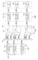
도 1은 본 발명의 실시예들에 따른 전원 공급 장치를 나타내는 블록도이다.
도 2, 3, 4, 5 및 6은 본 발명의 실시예들에 따른 전원 공급 장치의 동작을 설명하기 위한 도면들이다.
도 7은 본 발명의 실시예들에 따른 전원 공급 장치를 나타내는 블록도이다.
도 8a, 8b 및 8c는 본 발명의 실시예들에 따른 전원 공급 장치에 포함되는 레귤레이터의 예를 나타내는 회로도들이다.
도 9는 본 발명의 실시예들에 따른 전원 공급 장치의 제어 방법을 나타내는 순서도이다.
도 10은 도 9의 제1 내지 제M 기준 전원들의 값들을 설정하는 단계의 일 예를 나타내는 순서도이다.
도 11은 본 발명의 실시예들에 따른 테스트 시스템을 나타내는 블록도이다.1 is a block diagram illustrating a power supply device according to embodiments of the present invention.
2, 3, 4, 5 and 6 are diagrams for explaining the operation of a power supply device according to embodiments of the present invention.
7 is a block diagram illustrating a power supply device according to embodiments of the present invention.
8A, 8B, and 8C are circuit diagrams illustrating examples of regulators included in a power supply device according to embodiments of the present invention.
9 is a flowchart illustrating a control method of a power supply device according to embodiments of the present invention.
10 is a flowchart illustrating an example of a step of setting values of the first to M th reference power sources of FIG. 9 .
11 is a block diagram illustrating a test system according to embodiments of the present invention.
이하, 첨부한 도면들을 참조하여, 본 발명의 바람직한 실시예를 보다 상세하게 설명하고자 한다. 도면상의 동일한 구성요소에 대해서는 동일한 참조부호를 사용하고 동일한 구성요소에 대해서 중복된 설명은 생략한다.Hereinafter, with reference to the accompanying drawings, preferred embodiments of the present invention will be described in more detail. The same reference numerals are used for the same components in the drawings, and redundant descriptions of the same components are omitted.
도 1은 본 발명의 실시예들에 따른 전원 공급 장치를 나타내는 블록도이다.1 is a block diagram showing a power supply device according to embodiments of the present invention.
도 1을 참조하면, 전원 공급 장치(100)는 제1 전원 생성부(200), 선택부(400) 및 제2 전원 생성부(500)를 포함한다. 전원 공급 장치(100)는 전원 레일부(power rail)(300) 및 복수의 부하(load)들(600)을 더 포함할 수 있다.Referring to FIG. 1 , the
제1 전원 생성부(200)는 제1 내지 제M(M은 2 이상의 자연수) 스위칭 레귤레이터(switching regulator)들(210a, 210b, ..., 210m)을 포함한다. 제1 내지 제M 스위칭 레귤레이터들(210a~210m)은 입력 전원(IPWR)에 기초하여 제1 내지 제M 기준 전원들(RPWR1, RPWR2, ..., RPWRM)을 발생한다. 예를 들어, 제1 스위칭 레귤레이터(210a)는 입력 전원(IPWR)에 기초하여 제1 기준 전원(RPWR1)을 발생할 수 있고, 제2 스위칭 레귤레이터(210b)는 입력 전원(IPWR)에 기초하여 제2 기준 전원(RPWR2)을 발생할 수 있으며, 제M 스위칭 레귤레이터(210m)는 입력 전원(IPWR)에 기초하여 제M 기준 전원(RPWRM)을 발생할 수 있다. 예를 들어, 입력 전원(IPWR)은 전압 값일 수 있으며, 이에 따라 기준 전원들(RPWR1~RPWRM) 각각은 전압 값일 수 있다.The
스위칭 레귤레이터는 적어도 하나의 스위칭 소자를 포함하여 구현되며, 상기 스위칭 소자의 온/오프 동작을 고속으로 반복하여 스위칭 레귤레이터의 출력 전압이 조절된다. 스위칭 레귤레이터는 상대적으로 효율이 좋고 발열이 적은 것이 장점이나, 상대적으로 회로 구조가 복잡하고 상기와 같은 스위칭 동작에 의해 노이즈가 발생하는 단점이 있다.The switching regulator is implemented by including at least one switching element, and an output voltage of the switching regulator is adjusted by repeating an on/off operation of the switching element at high speed. The switching regulator has advantages of relatively high efficiency and low heat generation, but has a relatively complex circuit structure and noise generation due to the switching operation as described above.
선택부(400)는 제1 내지 제N(N은 2 이상의 자연수) 멀티플렉서들(410a, 410b, ..., 410n)을 포함한다. 제1 내지 제N 멀티플렉서들(410a~410n)은 전원 선택 신호(PSEL)를 기초로 제1 내지 제M 기준 전원들(RPWR1~RPWRM) 중 하나를 선택하여 제1 내지 제N 선택 전원들(SPWR1, SPWR2, ..., SPWRN)을 제공한다. 예를 들어, 전원 선택 신호(PSEL)는 제1 내지 제N 선택 신호들(S1, S2, ..., SN)을 포함할 수 있다. 제1 멀티플렉서(410a)는 제1 선택 신호(S1)에 기초하여 제1 내지 제M 기준 전원들(RPWR1~RPWRM) 중 하나를 제1 선택 전원(SPWR1)으로 출력할 수 있고, 제2 멀티플렉서(410b)는 제2 선택 신호(S2)에 기초하여 제1 내지 제M 기준 전원들(RPWR1~RPWRM) 중 하나를 제2 선택 전원(SPWR2)으로 출력할 수 있으며, 제N 멀티플렉서(410n)는 제N 선택 신호(SN)에 기초하여 제1 내지 제M 기준 전원들(RPWR1~RPWRM) 중 하나를 제N 선택 전원(SPWRN)으로 출력할 수 있다. 기준 전원들(RPWR1~RPWRM)과 유사하게, 선택 전원들(SPWR1~SPWRN) 각각은 전압 값일 수 있다.The
제2 전원 생성부(500)는 제1 내지 제N 선형 레귤레이터(linear regulator)들(510a, 510b, ..., 510n)을 포함한다. 제1 내지 제N 선형 레귤레이터들(510a~510n)은 제1 내지 제N 멀티플렉서들(410a~410n) 중 하나와 각각 연결되고, 제1 내지 제N 선택 전원들(SPWR1~SPWRN)에 기초하여 제1 내지 제N 출력 전원들(OPWR1, OPWR2, ..., OPWRN)을 발생한다. 예를 들어, 제1 선형 레귤레이터(510a)는 제1 멀티플렉서(410a)와 연결될 수 있고, 제1 선택 전원(SPWR1)에 기초하여 제1 출력 전원(OPWR1)을 발생할 수 있다. 제2 선형 레귤레이터(510b)는 제2 멀티플렉서(410b)와 연결될 수 있고, 제2 선택 전원(SPWR2)에 기초하여 제2 출력 전원(OPWR2)을 발생할 수 있다. 제N 선형 레귤레이터(510n)는 제N 멀티플렉서(410n)와 연결될 수 있고, 제N 선택 전원(SPWRN)에 기초하여 제N 출력 전원(OPWRN)을 발생할 수 있다. 선택 전원들(SPWR1~SPWRN)과 유사하게, 출력 전원들(OPWR1~OPWRN) 각각은 전압 값일 수 있다.The
선형 레귤레이터는 입력 전압과 출력 전압이 선형 관계를 가지도록 구현되며, 스위칭 레귤레이터와 다르게 스위칭 동작 없이 선형 레귤레이터의 출력 전압이 조절된다. 선형 레귤레이터는 상대적으로 회로 구조가 간단하고 노이즈가 적은 것이 장점이나, 상대적으로 효율이 떨어지고 발열이 큰 단점이 있다.The linear regulator is implemented so that the input voltage and the output voltage have a linear relationship, and unlike the switching regulator, the output voltage of the linear regulator is adjusted without a switching operation. The linear regulator has the advantage of having a relatively simple circuit structure and low noise, but has the disadvantage of relatively low efficiency and high heat generation.
일 실시예에서, 선형 레귤레이터에 의해 손실되는 전력은 선형 레귤레이터의 출력과 입력의 차이에 비례하여 증가할 수 있다. 예를 들어, 제1 선형 레귤레이터(510a)에 의해 손실되는 제1 손실 전력은 제1 출력 전원(OPWR1)과 제1 선택 전원(SPWR1)의 차이에 비례하여 증가할 수 있다.In one embodiment, the power dissipated by the linear regulator may increase proportionally to the difference between the output and input of the linear regulator. For example, the first loss power lost by the first
일 실시예에서, 도 2 내지 6을 참조하여 후술하는 것처럼, 기준 제어 신호(RCONT)에 기초하여 제1 내지 제M 기준 전원들(RPWR1~RPWRM)의 값들이 설정될 수 있고, 출력 제어 신호(OCONT)에 기초하여 제1 내지 제N 출력 전원들(OPWR1~OPWRN)의 값들이 설정될 수 있다. 예를 들어, 제1 내지 제N 출력 전원들(OPWR1~OPWRN)의 값들이 먼저 설정될 수 있고, 제1 내지 제N 선형 레귤레이터들(510a~510n)의 출력과 입력의 차이(즉, 드롭아웃(dropout))가 전체적으로 최적화되도록 상기 제1 내지 제M 기준 전원들(RPWR1~RPWRM)의 값들이 설정될 수 있다.In one embodiment, as will be described later with reference to FIGS. 2 to 6 , values of the first to M th reference power sources RPWR1 to RPWRM may be set based on the reference control signal RCONT, and the output control signal ( Values of the first to Nth output power supplies OPWR1 to OPWRN may be set based on OCONT. For example, the values of the first to Nth output power supplies OPWR1 to OPWRN may be set first, and the difference between the output and input of the first to Nth
일 실시예에서, 기준 제어 신호(RCONT), 전원 선택 신호(PSEL) 및 출력 제어 신호(OCONT)는 외부(예를 들어, 외부의 컨트롤러)로부터 수신될 수 있다.In an embodiment, the reference control signal RCONT, the power selection signal PSEL, and the output control signal OCONT may be received from an external source (eg, an external controller).
전원 레일부(300)는 제1 내지 제M 기준 전원들(RPWR1~RPWRM)을 제1 내지 제N 멀티플렉서들(410a~410n) 모두에 제공하도록 구현될 수 있다. 예를 들어, 전원 레일부(300)는 M*N개의 전원 배선들을 포함할 수 있다. 상기 M*N개의 전원 배선들은 제1 기준 전원(RPWR1)을 제1 내지 제N 멀티플렉서들(410a~410n)에 제공하기 위한 M개의 전원 배선들, 제2 기준 전원(RPWR2)을 제1 내지 제N 멀티플렉서들(410a~410n)에 제공하기 위한 M개의 전원 배선들, 제M 기준 전원(RPWRM)을 제1 내지 제N 멀티플렉서들(410a~410n)에 제공하기 위한 M개의 전원 배선들 등을 포함할 수 있다.The
복수의 부하들(600)은 제1 내지 제N 부하들(610a, 610b, ..., 610n)을 포함할 수 있다. 제1 내지 제N 부하들(610a~610n)은 제1 내지 제N 선형 레귤레이터들(510a~510n)과 각각 연결될 수 있고, 제1 내지 제N 출력 전원들(OPWR1~OPWRN)을 공급받을 수 있다. 예를 들어, 제1 부하(610a)는 제1 선형 레귤레이터(510a)와 연결되어 제1 출력 전원(OPWR1)을 공급받을 수 있고, 제2 부하(610b)는 제2 선형 레귤레이터(510b)와 연결되어 제2 출력 전원(OPWR2)을 공급받을 수 있으며, 제N 부하(610n)는 제N 선형 레귤레이터(510n)와 연결되어 제N 출력 전원(OPWRN)을 공급받을 수 있다.The plurality of
일 실시예에서, 스위칭 레귤레이터들(210a~210m)의 개수와 선형 레귤레이터들(510a~510n)의 개수는 서로 다를 수 있다. 다시 말하면, 스위칭 레귤레이터들(210a~210m)에 대한 채널 수와 선형 레귤레이터들(510a~510n)에 대한 채널 수는 서로 다를 수 있으며, M과 N은 서로 다른 자연수일 수 있다.In one embodiment, the number of
일 실시예에서, 선형 레귤레이터들(510a~510n)의 개수는 스위칭 레귤레이터들(210a~210m)의 개수보다 많을 수 있다. 다시 말하면, 선형 레귤레이터들(510a~510n)에 대한 채널 수는 스위칭 레귤레이터들(210a~210m)에 대한 채널 수보다 많을 수 있으며, N은 M보다 큰 자연수일 수 있다.In one embodiment, the number of
다른 실시예에서, 스위칭 레귤레이터들(210a~210m)의 개수와 선형 레귤레이터들(510a~510n)의 개수는 실질적으로 동일할 수도 있다.In another embodiment, the number of
본 발명의 실시예들에 따른 전원 공급 장치(100)는 스위칭 레귤레이터들(210a~210m)과 선형 레귤레이터들(510a~510n)이 멀티-채널(multi-channel) 형태로 병렬 연결되는 하이브리드(hybrid) 타입의 전원 공급 장치일 수 있다. 이 때, 선형 레귤레이터들(510a~510n) 각각에 최적의 입력을 제공할 수 있도록 선형 레귤레이터들(510a~510n)과 동일한 개수의 멀티플렉서들(410a~410n)을 포함하여 구현될 수 있다. 따라서, 전원 공급 장치(100)는 고효율 및 고성능 특성을 동시에 가지면서도 상대적으로 작은 크기 및 간단한 구조를 가질 수 있고, 선형 레귤레이터들(510a~510n)의 드롭아웃이 전체적으로 최적화되어 향상된 성능을 가질 수 있다.The
도 2, 3, 4, 5 및 6은 본 발명의 실시예들에 따른 전원 공급 장치의 동작을 설명하기 위한 도면들이다. 도 2, 3, 4, 5 및 6에서는 전원 공급 장치가 네 개의 스위칭 레귤레이터들(SR1, SR2, SR3, SR4) 및 일곱 개의 선형 레귤레이터들(LR1, LR2, LR3, LR4, LR5, LR6, LR7)을 포함하는 경우를 예시하였으며, 출력 전원들(OPWR1, OPWR2, OPWR3, OPWR4, OPWR5, OPWR6, OPWR7)의 값들 및 기준 전원들(RPWR1, RPWR2, RPWR3, RPWR4)의 값들을 설정하는 동작과 그 이후에 선택 신호들(S1, S2, S3, S4, S5, S6, S7) 및 선택 전원들(SPWR1, SPWR2, SPWR3, SPWR4, SPWR5, SPWR6, SPWR7)을 설정하는 동작을 도시하였다.2, 3, 4, 5 and 6 are diagrams for explaining the operation of a power supply device according to embodiments of the present invention. 2, 3, 4, 5 and 6, the power supply includes four switching regulators (SR1, SR2, SR3, SR4) and seven linear regulators (LR1, LR2, LR3, LR4, LR5, LR6, LR7) , and the operation of setting the values of the output power sources (OPWR1, OPWR2, OPWR3, OPWR4, OPWR5, OPWR6, OPWR7) and the values of the reference power sources (RPWR1, RPWR2, RPWR3, RPWR4) and thereafter An operation of setting the selection signals S1, S2, S3, S4, S5, S6, and S7 and the selection power sources SPWR1, SPWR2, SPWR3, SPWR4, SPWR5, SPWR6, and SPWR7 is shown in FIG.
도 2를 참조하면, 먼저 출력 제어 신호(도 1의 OCONT)에 기초하여 선형 레귤레이터들(LR1~LR7)에 대한 출력 전원들(OPWR1~OPWR7)의 값들이 설정될 수 있다. 예를 들어, 제1 선형 레귤레이터(LR1)의 제1 출력 전원(OPWR1)이 약 1.8V로 설정될 수 있고, 제2 선형 레귤레이터(LR2)의 제2 출력 전원(OPWR2)이 약 1V로 설정될 수 있고, 제3 선형 레귤레이터(LR3)의 제3 출력 전원(OPWR3)이 약 2V로 설정될 수 있고, 제4 선형 레귤레이터(LR4)의 제4 출력 전원(OPWR4)이 약 1.2V로 설정될 수 있고, 제5 선형 레귤레이터(LR5)의 제5 출력 전원(OPWR5)이 약 3.3V로 설정될 수 있고, 제6 선형 레귤레이터(LR6)의 제6 출력 전원(OPWR6)이 약 2.5V로 설정될 수 있으며, 제7 선형 레귤레이터(LR7)의 제7 출력 전원(OPWR7)이 약 1.5V로 설정될 수 있다.Referring to FIG. 2 , first, values of output power supplies OPWR1 to OPWR7 for linear regulators LR1 to LR7 may be set based on an output control signal (OCONT of FIG. 1 ). For example, the first output power OPWR1 of the first linear regulator LR1 may be set to about 1.8V, and the second output power OPWR2 of the second linear regulator LR2 may be set to about 1V. The third output power OPWR3 of the third linear regulator LR3 may be set to about 2V, and the fourth output power OPWR4 of the fourth linear regulator LR4 may be set to about 1.2V. , the fifth output power OPWR5 of the fifth linear regulator LR5 may be set to about 3.3V, and the sixth output power OPWR6 of the sixth linear regulator LR6 may be set to about 2.5V. , and the seventh output power OPWR7 of the seventh linear regulator LR7 may be set to about 1.5V.
일 실시예에서, 도 2에 도시된 것처럼 선형 레귤레이터들(LR1~LR7)의 출력 전원들(OPWR1~OPWR7) 모두가 서로 다른 값을 가지도록 설정될 수 있다. 다른 실시예에서, 도시하지는 않았지만 상기 선형 레귤레이터들의 출력 전원들 중 적어도 일부가 동일한 값을 가지도록 설정될 수도 있다.In one embodiment, as shown in FIG. 2 , all of the output power supplies OPWR1 to OPWR7 of the linear regulators LR1 to LR7 may be set to have different values. In another embodiment, although not shown, at least some of the output power supplies of the linear regulators may be set to have the same value.
도 3 및 4를 참조하면, 출력 제어 신호(도 1의 OCONT)에 기초하여 출력 전원들(OPWR1~OPWR7)의 값들이 설정된 이후에, 출력 전원들(OPWR1~OPWR7)이 전원 그룹들(PG1, PG2, PG3, PG4)로 그룹화될 수 있다.Referring to FIGS. 3 and 4 , after the values of the output power supplies OPWR1 to OPWR7 are set based on the output control signal (OCONT in FIG. PG2, PG3, and PG4).
구체적으로, 출력 전원들(OPWR1~OPWR7)을 전원 그룹들(PG1~PG4)로 그룹화하기 위해, 도 3에 도시된 것처럼 출력 전원들(OPWR1~OPWR7)이 미리 정해진 제1 규칙에 기초하여 정렬될 수 있다.Specifically, in order to group the output power supplies OPWR1 to OPWR7 into power groups PG1 to PG4, as shown in FIG. 3, the output power supplies OPWR1 to OPWR7 are arranged based on a first predetermined rule. can
일 실시예에서, 상기 제1 규칙은 출력 전원들(OPWR1~OPWR7)의 크기와 관련될 수 있다. 예를 들어, 출력 전원들(OPWR1~OPWR7)은 크기 순서로 정렬될 수 있다. 예를 들어, 도 3에 도시된 것처럼 출력 전원들(OPWR1~OPWR7)은 가장 작은 값(예를 들어, 약 1V)을 가지는 제2 출력 전원(OPWR2)부터 가장 큰 값(예를 들어, 약 3.3V)을 가지는 제5 출력 전원(OPWR5)까지 오름차순으로 정렬될 수 있다. 다른 예에서, 도시하지는 않았지만 상기 출력 전원들은 내림차순으로 정렬될 수도 있다.In one embodiment, the first rule may be related to the size of the output power supplies OPWR1 to OPWR7 . For example, the output power supplies OPWR1 to OPWR7 may be arranged in order of size. For example, as shown in FIG. 3 , the output power supplies OPWR1 to OPWR7 range from the second output power OPWR2 having the smallest value (eg, about 1V) to the largest value (eg, about 3.3 V). V) may be arranged in ascending order up to the fifth output power source OPWR5. In another example, although not shown, the output power supplies may be arranged in descending order.
다른 실시예에서, 상기 제1 규칙은 최적의 정렬을 위한 임의의 규칙일 수 있다. 도시하지는 않았지만, 이 경우 상기 출력 전원들은 임의의 규칙에 기초하여 정렬될 수 있다.In another embodiment, the first rule may be any rule for optimal alignment. Although not shown, in this case, the output power sources may be arranged based on an arbitrary rule.
또한, 도 4에 도시된 것처럼 정렬된 출력 전원들(OPWR1~OPWR7)이 미리 정해진 제2 규칙에 기초하여 전원 그룹들(PG1~PG4)로 그룹화될 수 있다. 전원 그룹들(PG1~PG4)의 개수는 스위칭 레귤레이터들(SR1~SR4)의 개수와 실질적으로 동일할 수 있다.Also, as shown in FIG. 4 , the aligned output power sources OPWR1 to OPWR7 may be grouped into power groups PG1 to PG4 based on a second predetermined rule. The number of power groups PG1 to PG4 may be substantially the same as the number of switching regulators SR1 to SR4.
일 실시예에서, 전원 그룹들(PG1~PG4) 각각은 출력 전원들(OPWR1~OPWR7) 중 적어도 하나를 포함할 수 있다. 예를 들어, 도 4에 도시된 것처럼, 제1 전원 그룹(PG1)은 제2 및 제4 출력 전원들(OPWR2, OPWR4)을 포함할 수 있고, 제2 전원 그룹(PG2)은 제1 및 제7 출력 전원들(OPWR1, OPWR7)을 포함할 수 있고, 제3 전원 그룹(PG3)은 제3 및 제6 출력 전원들(OPWR3, OPWR6)을 포함할 수 있으며, 제4 전원 그룹(PG4)은 제5 출력 전원(OPWR5)을 포함할 수 있다. 다시 말하면, 전원 그룹들(PG1~PG4) 중 출력 전원을 포함하지 않는, 즉 비어있는 전원 그룹은 존재하지 않을 수 있다.In one embodiment, each of the power groups PG1 to PG4 may include at least one of the output power sources OPWR1 to OPWR7 . For example, as shown in FIG. 4 , the first power group PG1 may include second and fourth output power sources OPWR2 and OPWR4, and the second power group PG2 may include the first and fourth output power sources OPWR2 and OPWR4. 7 output power sources OPWR1 and OPWR7 may be included, the third power group PG3 may include third and sixth output power sources OPWR3 and OPWR6, and the fourth power group PG4 may include A fifth output power source OPWR5 may be included. In other words, among the power groups PG1 to PG4, there may be no power group that does not include output power, that is, an empty power group.
일 실시예에서, 출력 전원들(OPWR1~OPWR7)이 크기 순서로 정렬된 경우에, 출력 전원들(OPWR1~OPWR7) 중 가장 작은 값을 갖는 최소 출력 전원 및 가장 큰 값을 갖는 최대 출력 전원 중 하나는 첫 번째 전원 그룹에 포함될 수 있고, 상기 최소 출력 전원 및 상기 최대 출력 전원 중 다른 하나는 마지막 전원 그룹에 포함될 수 있다. 예를 들어, 도 3 및 4에 도시된 것처럼 출력 전원들(OPWR1~OPWR7)이 오름차순으로 정렬된 경우에, 상기 최소 출력 전원(예를 들어, OPWR2)이 상기 첫 번째 전원 그룹(예를 들어, PG1)에 포함될 수 있고, 상기 최대 출력 전원(예를 들어, OPWR5)이 상기 마지막 전원 그룹(예를 들어, PG4)에 포함될 수 있다. 다른 예에서, 도시하지는 않았지만 상기 출력 전원들이 내림차순으로 정렬된 경우에, 상기 최대 출력 전원이 상기 첫 번째 전원 그룹에 포함될 수 있고, 상기 최소 출력 전원이 상기 마지막 전원 그룹에 포함될 수 있다.In one embodiment, when the output power supplies OPWR1 to OPWR7 are arranged in order of magnitude, one of a minimum output power having the smallest value and a maximum output power having the largest value among the output power supplies OPWR1 to OPWR7 . may be included in the first power group, and the other one of the minimum output power and the maximum output power may be included in the last power group. For example, as shown in FIGS. 3 and 4 , when the output power supplies (OPWR1 to OPWR7) are arranged in ascending order, the minimum output power (eg, OPWR2) is the first power group (eg, PG1), and the maximum output power (eg, OPWR5) may be included in the last power group (eg, PG4). In another example, although not shown, when the output power sources are arranged in descending order, the maximum output power may be included in the first power group and the minimum output power may be included in the last power group.
일 실시예에서, 상기 제2 규칙은 각 전원 그룹에 포함되는 출력 전원들의 개수와 관련될 수 있다. 예를 들어, 하나의 전원 그룹에 포함되는 출력 전원들의 개수가 유사하도록 출력 전원들(OPWR1~OPWR7)이 그룹화될 수 있다. 예를 들어, 도 4에 도시된 것처럼 일곱 개의 출력 전원들(OPWR1~OPWR7)을 네 개의 전원 그룹들(PG1~PG4)로 그룹화하는 경우에, 7/4=1.75이므로 하나의 전원 그룹이 1개 또는 2개의 출력 전원들을 포함하도록 그룹화될 수 있다.In one embodiment, the second rule may be related to the number of output power sources included in each power group. For example, the output power supplies OPWR1 to OPWR7 may be grouped so that the number of output power supplies included in one power supply group is similar. For example, as shown in FIG. 4 , when seven output power supplies (OPWR1 to OPWR7) are grouped into four power supply groups (PG1 to PG4), one power group is 1 because 7/4 = 1.75. or grouped to include two output power supplies.
다른 실시예에서, 상기 제2 규칙은 출력 전원들(OPWR1~OPWR7)의 값들과 관련될 수 있다. 예를 들어, 문턱 전원 값들에 기초하여 출력 전원들(OPWR1~OPWR7)이 그룹화될 수 있다. 예를 들어, 도 4에 도시된 것처럼 일곱 개의 출력 전원들(OPWR1~OPWR7)을 네 개의 전원 그룹들(PG1~PG4)로 그룹화하는 경우에, 제1, 제2 및 제3 문턱 전원 값들이 각각 약 1.5V, 2V, 3V로 설정될 수 있다. 상기 제1 문턱 전원 값보다 작은 적어도 하나의 출력 전원(예를 들어, OPWR2 및 OPWR4)이 제1 전원 그룹(PG1)에 포함될 수 있고, 상기 제1 문턱 전원 값보다 크거나 같고 상기 제2 문턱 전원 값보다 작은 적어도 하나의 출력 전원(예를 들어, OPWR1 및 OPWR7)이 제2 전원 그룹(PG2)에 포함될 수 있고, 상기 제2 문턱 전원 값보다 크거나 같고 상기 제3 문턱 전원 값보다 작은 적어도 하나의 출력 전원(예를 들어, OPWR3 및 OPWR6)이 제3 전원 그룹(PG3)에 포함될 수 있으며, 상기 제3 문턱 전원 값보다 크거나 같은 적어도 하나의 출력 전원(예를 들어, OPWR5)이 제4 전원 그룹(PG4)에 포함될 수 있다.In another embodiment, the second rule may be related to values of the output power supplies OPWR1 to OPWR7 . For example, the output power supplies OPWR1 to OPWR7 may be grouped based on threshold power values. For example, as shown in FIG. 4 , when seven output power supplies OPWR1 to OPWR7 are grouped into four power groups PG1 to PG4, first, second, and third threshold power values are respectively It can be set to about 1.5V, 2V, or 3V. At least one output power (for example, OPWR2 and OPWR4) smaller than the first threshold power value may be included in the first power group PG1 and greater than or equal to the first threshold power value, and the second threshold power value is greater than or equal to the first threshold power value. At least one output power (eg, OPWR1 and OPWR7) smaller than the value may be included in the second power group PG2, and at least one output power greater than or equal to the second threshold power value and less than the third threshold power value may be included in the second power group PG2. of output powers (eg, OPWR3 and OPWR6) may be included in the third power group PG3, and at least one output power greater than or equal to the third threshold power value (eg, OPWR5) may be included in the fourth power group. It may be included in the power group PG4.
또 다른 실시예에서, 상기 제2 규칙은 최적의 그룹화를 위한 임의의 규칙일 수 있다. 도시하지는 않았지만, 이 경우 상기 출력 전원들은 임의의 규칙에 기초하여 그룹화될 수 있다.In another embodiment, the second rule may be any rule for optimal grouping. Although not shown, in this case, the output power sources may be grouped based on an arbitrary rule.
도 5를 참조하면, 출력 전원들(OPWR1~OPWR7)이 전원 그룹들(PG1~PG4)로 그룹화된 이후에, 기준 제어 신호(도 1의 RCONT)에 기초하여 전원 그룹들(PG1~PG4)에 대한 기준 전원들(RPWR1~RPWR4)의 값들이 설정될 수 있다. 예를 들어, 제1 전원 그룹(PG1)에 대한 제1 기준 전원(RPWR1)이 약 3.2V로 설정될 수 있고, 제2 전원 그룹(PG2)에 대한 제2 기준 전원(RPWR2)이 약 3.8V로 설정될 수 있고, 제3 전원 그룹(PG3)에 대한 제3 기준 전원(RPWR3)이 약 4.5V로 설정될 수 있으며, 제4 전원 그룹(PG4)에 대한 제4 기준 전원(RPWR4)이 약 5.3V로 설정될 수 있다. 기준 전원들(RPWR1~RPWR4)의 값들은 미리 정해진 제3 규칙에 기초하여 설정될 수 있다.Referring to FIG. 5 , after the output power supplies OPWR1 to OPWR7 are grouped into power groups PG1 to PG4, the power groups PG1 to PG4 are assigned to the power groups PG1 to PG4 based on the reference control signal (RCONT of FIG. 1). Values of the reference power sources RPWR1 to RPWR4 may be set. For example, the first reference power supply RPWR1 for the first power group PG1 may be set to about 3.2V, and the second reference power supply RPWR2 for the second power group PG2 is about 3.8V. , the third reference power supply RPWR3 for the third power group PG3 may be set to about 4.5V, and the fourth reference power supply RPWR4 for the fourth power group PG4 is about It can be set to 5.3V. Values of the reference power sources RPWR1 to RPWR4 may be set based on a third predetermined rule.
일 실시예에서, 상기 제3 규칙은 각 전원 그룹에 포함되는 출력 전원들의 값들과 관련될 수 있다. 예를 들어, 각 기준 전압의 값은 각 전원 그룹에 포함되는 출력 전원들 중에서 가장 큰 값을 갖는 출력 전원보다 크도록 설정될 수 있으며, 상기 가장 큰 출력 전원의 값에 오프셋 값을 더하여 획득될 수 있다. 예를 들어, 도 4에 도시된 것처럼 상기 오프셋 값은 약 2V일 수 있다. 제1 기준 전원(RPWR1)은 제1 전원 그룹(PG1)에서 가장 큰 값을 갖는 제1 최대 출력 전원인 약 1.2V에 상기 오프셋 값을 더하여 획득될 수 있고, 제2 기준 전원(RPWR2)은 제2 전원 그룹(PG2)에서 가장 큰 값을 갖는 제2 최대 출력 전원인 약 1.8V에 상기 오프셋 값을 더하여 획득될 수 있고, 제3 기준 전원(RPWR3)은 제3 전원 그룹(PG3)에서 가장 큰 값을 갖는 제3 최대 출력 전원인 약 2.5V에 상기 오프셋 값을 더하여 획득될 수 있으며, 제4 기준 전원(RPWR4)은 제4 전원 그룹(PG4)에서 가장 큰 값을 갖는 제4 최대 출력 전원인 약 3.3V에 상기 오프셋 값을 더하여 획득될 수 있다.In one embodiment, the third rule may relate to values of output powers included in each power group. For example, the value of each reference voltage may be set to be greater than the output power having the largest value among the output powers included in each power group, and may be obtained by adding an offset value to the value of the largest output power. there is. For example, as shown in FIG. 4 , the offset value may be about 2V. The first reference power supply RPWR1 may be obtained by adding the offset value to about 1.2V, which is the first maximum output power having the largest value in the first power group PG1, and the second reference power supply RPWR2 may be It can be obtained by adding the offset value to about 1.8V, which is the second maximum output power having the largest value in the second power group PG2, and the third reference power RPWR3 is the largest in the third power group PG3. It can be obtained by adding the offset value to the third maximum output power having a value of about 2.5V, and the fourth reference power supply RPWR4 is the fourth maximum output power having the largest value in the fourth power group PG4. It can be obtained by adding the above offset value to about 3.3V.
다른 실시예에서, 상기 제3 규칙은 최적의 효율 및 최소의 드롭아웃을 구현하기 위한 임의의 규칙일 수 있다. 도시하지는 않았지만, 이 경우 상기 기준 전원들은 임의의 규칙에 기초하여 설정될 수 있다.In another embodiment, the third rule may be any rule for implementing optimal efficiency and minimum dropout. Although not shown, in this case, the reference power sources may be set based on an arbitrary rule.
도 6을 참조하면, 출력 전원들(OPWR1~OPWR7)의 값들 및 기준 전원들(RPWR1~RPWR4)의 값들이 설정된 이후에, 멀티플렉서들(MUX1, MUX2, MUX3, MUX4, MUX5, MUX6, MUX7)이 선형 레귤레이터들(LR1~LR7)에 적합한 최적의 선택 전원들(SPWR1~SPWR7)을 제공하도록, 전원 선택 신호(도 1의 PSEL)에 포함되는 선택 신호들(S1~S7)이 설정될 수 있다.Referring to FIG. 6, after the values of the output power sources OPWR1 to OPWR7 and the values of the reference power sources RPWR1 to RPWR4 are set, the multiplexers MUX1, MUX2, MUX3, MUX4, MUX5, MUX6, and MUX7 are Selection signals S1 to S7 included in the power selection signal (PSEL of FIG. 1 ) may be set to provide optimum selection power supplies SPWR1 to SPWR7 suitable for the linear regulators LR1 to LR7.
구체적으로, 제1 멀티플렉서(MUX1)가 전원 레일부(PR)를 통해 제공된 기준 전원들(RPWR1~RPWR4) 중 제2 기준 전원(RPWR2)을 제1 선택 전원(SPWR1)으로 출력하도록, 제1 선택 신호(S1)가 설정될 수 있다. 제2 멀티플렉서(MUX2)가 제1 기준 전원(RPWR1)을 제2 선택 전원(SPWR2)으로 출력하도록, 제2 선택 신호(S2)가 설정될 수 있다. 제3 멀티플렉서(MUX3)가 제3 기준 전원(RPWR3)을 제3 선택 전원(SPWR3)으로 출력하도록, 제3 선택 신호(S3)가 설정될 수 있다. 제4 멀티플렉서(MUX4)가 제1 기준 전원(RPWR1)을 제4 선택 전원(SPWR4)으로 출력하도록, 제4 선택 신호(S4)가 설정될 수 있다. 제5 멀티플렉서(MUX5)가 제4 기준 전원(RPWR4)을 제5 선택 전원(SPWR5)으로 출력하도록, 제5 선택 신호(S5)가 설정될 수 있다. 제6 멀티플렉서(MUX6)가 제3 기준 전원(RPWR3)을 제6 선택 전원(SPWR6)으로 출력하도록, 제6 선택 신호(S6)가 설정될 수 있다. 제7 멀티플렉서(MUX7)가 제2 기준 전원(RPWR2)을 제7 선택 전원(SPWR7)으로 출력하도록, 제7 선택 신호(S7)가 설정될 수 있다.Specifically, the first multiplexer MUX1 outputs the second reference power supply RPWR2 among the reference power supplies RPWR1 to RPWR4 provided through the power rail unit PR as the first selected power supply SPWR1. Signal S1 can be set. The second selection signal S2 may be set so that the second multiplexer MUX2 outputs the first reference power supply RPWR1 as the second selection power supply SPWR2. The third selection signal S3 may be set so that the third multiplexer MUX3 outputs the third reference power supply RPWR3 as the third selection power supply SPWR3. The fourth selection signal S4 may be set so that the fourth multiplexer MUX4 outputs the first reference power supply RPWR1 as the fourth selection power supply SPWR4. The fifth selection signal S5 may be set so that the fifth multiplexer MUX5 outputs the fourth reference power supply RPWR4 as the fifth selection power supply SPWR5. The sixth selection signal S6 may be set so that the sixth multiplexer MUX6 outputs the third reference power supply RPWR3 as the sixth selection power supply SPWR6. The seventh selection signal S7 may be set so that the seventh multiplexer MUX7 outputs the second reference power supply RPWR2 as the seventh selection power supply SPWR7.
다시 말하면, 멀티플렉서들(MUX1~MUX7)은 선택 신호들(S1~S7)에 기초하여 선형 레귤레이터들(LR1~LR7)과 이에 대응하는 최적의 스위칭 레귤레이터들(SR1~SR4)을 전기적으로 연결할 수 있다. 예를 들어, 제1 전원 그룹(PG1)과 관련된 제2 및 제4 선형 레귤레이터들(LR2, LR4)은 최적의 효율 및 드롭아웃을 구현하기 위해 제2 및 제4 멀티플렉서들(MUX2, MUX4)을 통해 제1 스위칭 레귤레이터(SR1)와 전기적으로 연결될 수 있다. 제2 전원 그룹(PG2)과 관련된 제1 및 제7 선형 레귤레이터들(LR1, LR7)은 최적의 효율 및 드롭아웃을 구현하기 위해 제1 및 제7 멀티플렉서들(MUX1, MUX7)을 통해 제2 스위칭 레귤레이터(SR2)와 전기적으로 연결될 수 있다. 제3 전원 그룹(PG3)과 관련된 제3 및 제6 선형 레귤레이터들(LR3, LR6)은 최적의 효율 및 드롭아웃을 구현하기 위해 제3 및 제6 멀티플렉서들(MUX3, MUX6)을 통해 제3 스위칭 레귤레이터(SR3)와 전기적으로 연결될 수 있다. 제4 전원 그룹(PG4)과 관련된 제5 선형 레귤레이터(LR5)는 최적의 효율 및 드롭아웃을 구현하기 위해 제5 멀티플렉서(MUX5)를 통해 제4 스위칭 레귤레이터(SR4)와 전기적으로 연결될 수 있다.In other words, the multiplexers MUX1 to MUX7 may electrically connect the linear regulators LR1 to LR7 and the corresponding optimal switching regulators SR1 to SR4 based on the selection signals S1 to S7. . For example, the second and fourth linear regulators LR2 and LR4 associated with the first power group PG1 include the second and fourth multiplexers MUX2 and MUX4 to implement optimal efficiency and dropout. Through this, it may be electrically connected to the first switching regulator SR1. The first and seventh linear regulators LR1 and LR7 associated with the second power group PG2 are switched through the first and seventh multiplexers MUX1 and MUX7 to achieve optimal efficiency and dropout. It may be electrically connected to the regulator SR2. The third and sixth linear regulators LR3 and LR6 associated with the third power group PG3 perform third switching through the third and sixth multiplexers MUX3 and MUX6 to implement optimal efficiency and dropout. It may be electrically connected to the regulator (SR3). The fifth linear regulator LR5 associated with the fourth power group PG4 may be electrically connected to the fourth switching regulator SR4 through the fifth multiplexer MUX5 to implement optimal efficiency and dropout.
일 실시예에서, 선택 신호들(S1~S7) 각각은 이진 신호일 수 있고, 상기 이진 신호의 비트 수는 전원 그룹들(PG1~PG4)의 개수 및 스위칭 레귤레이터들(SR1~SR4)의 개수와 실질적으로 동일할 수 있다. 도 6의 예에서, 선택 신호들(S1~S7) 각각은 4비트의 이진 신호일 수 있으며, 논리 하이 레벨(예를 들어, "1")에 대응하는 기준 전원이 선택 전원으로 출력될 수 있다. 예를 들어, 제2 및 제4 선택 신호들(S2, S4)은 제1 기준 전원(RPWR1)을 출력하도록 최하위 비트(least significant bit; LSB)만이 논리 하이 레벨(예를 들어, "1")을 갖는 "0001"로 설정될 수 있다. 제1 및 제7 선택 신호들(S1, S7)은 제2 기준 전원(RPWR2)을 출력하도록 두 번째 하위 비트만이 상기 논리 하이 레벨을 갖는 "0010"으로 설정될 수 있다. 제3 및 제6 선택 신호들(S3, S6)은 제3 기준 전원(RPWR3)을 출력하도록 차상위 비트만이 상기 논리 하이 레벨을 갖는 "0100"으로 설정될 수 있다. 제5 선택 신호(S5)는 제4 기준 전원(RPWR4)을 출력하도록 최상위 비트(most significant bit; MSB)만이 상기 논리 하이 레벨을 갖는 "1000"으로 설정될 수 있다.In one embodiment, each of the selection signals S1 to S7 may be a binary signal, and the number of bits of the binary signal is substantially equal to the number of power groups PG1 to PG4 and the number of switching regulators SR1 to SR4. can be the same as In the example of FIG. 6 , each of the selection signals S1 to S7 may be a 4-bit binary signal, and a reference power corresponding to a logic high level (eg, “1”) may be output as the selected power. For example, only the least significant bit (LSB) of the second and fourth selection signals S2 and S4 is a logic high level (eg, "1") to output the first reference power source RPWR1. It can be set to "0001" with Only the second lower bit of the first and seventh selection signals S1 and S7 may be set to “0010” having the logic high level so as to output the second reference power supply RPWR2. The third and sixth selection signals S3 and S6 may be set to "0100" having the logic high level only in the next higher order bit so as to output the third reference power supply RPWR3. The fifth selection signal S5 may be set to “1000” having only the most significant bit (MSB) having the logic high level so as to output the fourth reference power source RPWR4.
선형 레귤레이터들(LR1~LR7)은 드롭아웃이 최적화되도록 설정된 선택 전원들(SPWR1~SPWR7)에 기초하여 출력 전원들(OPWR1~OPWR7)을 발생할 수 있으며, 따라서 향상된 성능을 가질 수 있다.The linear regulators LR1 to LR7 may generate the output power supplies OPWR1 to OPWR7 based on the selected power supplies SPWR1 to SPWR7 set to optimize dropout, and thus may have improved performance.
도 2 내지 6을 참조하여 기준 전원들(RPWR1~RPWR4), 선택 전원들(SPWR1~SPWR7) 및 출력 전원들(OPWR1~OPWR7)을 설정하는 일 예를 설명하였으나, 실시예에 따라서 상기 기준 전원들, 상기 선택 전원들 및 상기 출력 전원들 중 적어도 하나는 가변될 수 있다. 다시 말하면, 본 발명의 실시예들에 따른 전원 공급 장치(100)에서 발생하고자 하는 목표 전원들(즉, 상기 출력 전원들)은 적용 대상 및/또는 동작 환경에 따라서 변경 가능하며, 상기 목표 전원들이 변경되는 경우에 상기 기준 전원들, 상기 선택 전원들 및 상기 출력 전원들이 최적화되도록 전원 공급 장치(100)가 동적으로(dynamically) 제어될 수 있다.An example of setting the reference power sources RPWR1 to RPWR4, the selected power sources SPWR1 to SPWR7, and the output power sources OPWR1 to OPWR7 has been described with reference to FIGS. 2 to 6, but according to the embodiment, the reference power sources , At least one of the selected power sources and the output power sources may be variable. In other words, the target power sources (i.e., the output power sources) to be generated by the
한편, 도 2 내지 6을 참조하여 상술한 레귤레이터들(SR1~SR4, LR1, LR7) 및 멀티플렉서들(MUX1~MUX7)의 개수와 이에 따른 전원들(RPWR1~RPWR4, SPWR1~SPWR7, OPWR1~OPWR7) 및 선택 신호들(S1~S7)의 개수, 전원들(RPWR1~RPWR4, SPWR1~SPWR7, OPWR1~OPWR7) 및 선택 신호들(S1~S7)의 값 등은 실시예에 따라서 다양하게 변경될 수 있다.On the other hand, the number of regulators (SR1 to SR4, LR1, LR7) and multiplexers (MUX1 to MUX7) described above with reference to FIGS. 2 to 6 and the corresponding power supplies (RPWR1 to RPWR4, SPWR1 to SPWR7, OPWR1 to OPWR7) The number of selection signals S1 to S7, the power supplies RPWR1 to RPWR4, SPWR1 to SPWR7, and OPWR1 to OPWR7, and the values of the selection signals S1 to S7 may be variously changed according to embodiments. .
도 7은 본 발명의 실시예들에 따른 전원 공급 장치를 나타내는 블록도이다.7 is a block diagram illustrating a power supply device according to embodiments of the present invention.
도 7을 참조하면, 전원 공급 장치(100a)는 제1 전원 생성부(200), 선택부(400) 및 제2 전원 생성부(500)를 포함하며, 전원 레일부(300), 복수의 부하들(600) 및 컨트롤러(700)를 더 포함할 수 있다.Referring to FIG. 7 , the
컨트롤러(700)를 더 포함하는 것을 제외하면, 도 7의 전원 공급 장치(100a)는 도 1의 전원 공급 장치(100)와 실질적으로 동일할 수 있다.Except for further including a
컨트롤러(700)는 기준 제어 신호(RCONT), 전원 선택 신호(PSEL) 및 출력 제어 신호(OCONT)를 발생할 수 있다. 기준 제어 신호(RCONT)에 기초하여 제1 내지 제M 기준 전원들(RPWR1~RPWRM)의 값들이 설정될 수 있고, 출력 제어 신호(OCONT)에 기초하여 제1 내지 제N 출력 전원들(OPWR1~OPWRN)의 값들이 설정될 수 있으며, 전원 선택 신호(PSEL)에 기초하여 제1 내지 제N 멀티플렉서들(410a~410n)에서 출력되는 제1 내지 제N 선택 전원들(SPWR1~SPWRN)이 결정될 수 있다. 예를 들어, 도 2 내지 6을 참조하여 상술한 방식에 기초하여 전원들이 설정될 수 있다.The
일 실시예에서, 기준 제어 신호(RCONT), 전원 선택 신호(PSEL) 및 출력 제어 신호(OCONT)에 기초하여 기준 전원들(RPWR1~RPWRM), 선택 전원들(SPWR1~SPWRN) 및 출력 전원들(OPWR1~OPWRN) 중 적어도 하나는 가변될 수 있다. 적용 대상 및/또는 동작 환경에 따라서 출력 전원들(OPWR1~OPWRN)이 변경되는 경우에, 기준 전원들(RPWR1~RPWRM), 선택 전원들(SPWR1~SPWRN) 및 출력 전원들(OPWR1~OPWRN)이 최적화되도록 전원 공급 장치(100a)가 동적으로 제어될 수 있다.In one embodiment, the reference power sources RPWR1 to RPWRM, the selected power sources SPWR1 to SPWRN, and the output power sources (RPWR1 to RPWRM) based on the reference control signal RCONT, the power selection signal PSEL, and the output control signal OCONT. At least one of OPWR1 to OPWRN) may be variable. When the output power supplies (OPWR1 to OPWRN) are changed according to the application target and/or operating environment, the reference power supplies (RPWR1 to RPWRM), the selected power supplies (SPWR1 to SPWRN), and the output power supplies (OPWR1 to OPWRN) are The
도 8a, 8b 및 8c는 본 발명의 실시예들에 따른 전원 공급 장치에 포함되는 레귤레이터의 예를 나타내는 회로도들이다. 도 8a 및 8b는 스위칭 레귤레이터의 예를 나타내며, 도 8c는 선형 레귤레이터의 예를 나타낸다.8A, 8B, and 8C are circuit diagrams illustrating examples of regulators included in a power supply device according to embodiments of the present invention. 8A and 8B show an example of a switching regulator, and FIG. 8C shows an example of a linear regulator.
스위칭 레귤레이터는 입력 전압과 출력 전압이 모두 직류(direct current; DC) 전압인 DC-DC 컨버터를 포함할 수 있다. 상기 DC-DC 컨버터는 벅 컨버터(buck converter 또는 step-down converter), 부스트 컨버터(boost converter 또는 step-up converter), 상기 벅 컨버터와 상기 부스트 컨버터가 결합된 벅-부스트 컨버터(buck-boost converter), 고립형(isolated) DC-DC 컨버터 등을 포함할 수 있다.The switching regulator may include a DC-DC converter in which both the input voltage and the output voltage are direct current (DC) voltages. The DC-DC converter is a buck converter (buck converter or step-down converter), a boost converter (boost converter or step-up converter), and a buck-boost converter in which the buck converter and the boost converter are combined , an isolated DC-DC converter, and the like.
도 8a를 참조하면, 상기 DC-DC 컨버터의 한 종류인 벅 컨버터는 스위치(SW1), 다이오드(D1), 인덕터(L1), 커패시터(C1) 및 저항(R1)을 포함할 수 있다.Referring to FIG. 8A , a buck converter, which is one type of the DC-DC converter, may include a switch SW1, a diode D1, an inductor L1, a capacitor C1, and a resistor R1.
스위치(SW1)는 제1 단자(T11)와 제1 노드(N11) 사이에 연결될 수 있고, 스위치 제어 신호(SC1)에 응답하여 온/오프될 수 있다. 다이오드(D1)는 제1 노드(N11)와 제2 노드(N12) 사이에 연결될 수 있다. 인덕터(L1)는 제1 노드(N11)와 제2 단자(T12) 사이에 연결될 수 있다. 커패시터(C1) 및 저항(R1)은 제2 단자(T12)와 제2 노드(N12) 사이에 병렬 연결될 수 있다. 상기 벅 컨버터에서, 제2 단자(T12)와 제2 노드(N12) 사이의 출력 전압(VOUT1)은 제1 단자(T11)와 제2 노드(N12) 사이의 입력 전압(VIN1)보다 작을 수 있다.The switch SW1 may be connected between the first terminal T11 and the first node N11 and may be turned on/off in response to the switch control signal SC1. The diode D1 may be connected between the first node N11 and the second node N12. The inductor L1 may be connected between the first node N11 and the second terminal T12. A capacitor C1 and a resistor R1 may be connected in parallel between the second terminal T12 and the second node N12. In the buck converter, the output voltage VOUT1 between the second terminal T12 and the second node N12 may be smaller than the input voltage VIN1 between the first terminal T11 and the second node N12. .
도 8b를 참조하면, 상기 DC-DC 컨버터의 다른 종류인 부스트 컨버터는 인덕터(L2), 스위치(SW2), 다이오드(D2), 커패시터(C2) 및 저항(R2)을 포함할 수 있다.Referring to FIG. 8B , the boost converter, which is another type of the DC-DC converter, may include an inductor L2, a switch SW2, a diode D2, a capacitor C2, and a resistor R2.
인덕터(L2)는 제1 단자(T21)와 제1 노드(N21) 사이에 연결될 수 있다. 스위치(SW2)는 제1 노드(N21)와 제2 노드(N22) 사이에 연결될 수 있고, 스위치 제어 신호(SC2)에 응답하여 온/오프될 수 있다. 다이오드(D2)는 제1 노드(N21)와 제2 단자(T22) 사이에 연결될 수 있다. 커패시터(C2) 및 저항(R2)은 제2 단자(T22)와 제2 노드(N22) 사이에 병렬 연결될 수 있다. 상기 부스트 컨버터에서, 제2 단자(T22)와 제2 노드(N22) 사이의 출력 전압(VOUT2)은 제1 단자(T21)와 제2 노드(N22) 사이의 입력 전압(VIN2)보다 클 수 있다.The inductor L2 may be connected between the first terminal T21 and the first node N21. The switch SW2 may be connected between the first node N21 and the second node N22 and may be turned on/off in response to the switch control signal SC2. The diode D2 may be connected between the first node N21 and the second terminal T22. A capacitor C2 and a resistor R2 may be connected in parallel between the second terminal T22 and the second node N22. In the boost converter, the output voltage VOUT2 between the second terminal T22 and the second node N22 may be greater than the input voltage VIN2 between the first terminal T21 and the second node N22. .
일 실시예에서, 스위치 제어 신호(도 8a의 SC1 또는 도 8b의 SC2)는 펄스 폭 변조(pulse width modulation; PWM) 방식 또는 펄스 주파수 변조(pulse frequency modulation; PFM) 방식에 기초하여 발생될 수 있다. 일 실시예에서, 스위치 제어 신호(도 8a의 SC1 또는 도 8b의 SC2)는 제2 단자(도 8a의 T12 또는 도 8b의 T22)로부터 피드백된 피드백 신호에 기초하여 발생될 수 있다.In one embodiment, the switch control signal (SC1 in FIG. 8A or SC2 in FIG. 8B) may be generated based on a pulse width modulation (PWM) method or a pulse frequency modulation (PFM) method. . In one embodiment, the switch control signal (SC1 in FIG. 8A or SC2 in FIG. 8B) may be generated based on a feedback signal fed back from the second terminal (T12 in FIG. 8A or T22 in FIG. 8B).
선형 레귤레이터는 션트(shunt) 레귤레이터, 시리즈(series) 레귤레이터, LDO(low dropout) 레귤레이터 등을 포함할 수 있다.Linear regulators may include shunt regulators, series regulators, low dropout (LDO) regulators, and the like.
도 8c를 참조하면, 선형 레귤레이터는 저항들(RA, RB) 및 제어 회로(10)를 포함할 수 있다.Referring to FIG. 8C , the linear regulator may include resistors RA and RB and a
저항(RA)은 제1 단자(TA1)와 제2 단자(TA2) 사이에 연결될 수 있고, 가변 저항일 수 있다. 저항(RB)은 제2 단자(TA2)와 제1 노드(NA1) 사이에 연결될 수 있다. 제어 회로(10)는 제2 단자(TA2)에서 피드백되는 피드백 신호에 기초하여 저항(RA)의 저항 값을 조절하는 저항 제어 신호(RC1)를 발생할 수 있다. 상기 선형 레귤레이터에서, 제2 단자(TA2)와 제1 노드(NA1) 사이의 출력 전압(VOUTA)은 제1 단자(TA1)와 제1 노드(NA1) 사이의 입력 전압(VINA)보다 작을 수 있다.The resistor RA may be connected between the first terminal TA1 and the second terminal TA2 and may be a variable resistor. The resistor RB may be connected between the second terminal TA2 and the first node NA1. The
도시하지는 않았지만, 스위칭 레귤레이터 및 선형 레귤레이터의 구조는 실시예에 따라서 다양하게 변경될 수 있다.Although not shown, structures of the switching regulator and the linear regulator may be variously changed according to embodiments.
도 9는 본 발명의 실시예들에 따른 전원 공급 장치의 제어 방법을 나타내는 순서도이다. 도 10은 도 9의 제1 내지 제M 기준 전원들의 값들을 설정하는 단계의 일 예를 나타내는 순서도이다.9 is a flowchart illustrating a control method of a power supply device according to embodiments of the present invention. 10 is a flowchart illustrating an example of a step of setting values of the first to M th reference power sources of FIG. 9 .
도 1 및 9를 참조하면, 제1 내지 제M 스위칭 레귤레이터들(210a~210m), 제1 내지 제N 멀티플렉서들(410a~410n) 및 제1 내지 제N 선형 레귤레이터들(510a~510n)을 포함하는 본 발명의 실시예들에 따른 전원 공급 장치(100)의 제어 방법에서, 출력 제어 신호(OCONT)에 기초하여 제1 내지 제N 출력 전원들(OPWR1~OPWRN)의 값들을 설정한다(단계 S100). 예를 들어, 도 2를 참조하여 상술한 것처럼 출력 전원들(OPWR1~OPWRN) 모두가 서로 다른 값을 가질 수 있다. 다른 예에서, 출력 전원들(OPWR1~OPWRN) 중 적어도 일부가 동일한 값을 가질 수도 있다.Referring to FIGS. 1 and 9 , the first to Mth switching
일 실시예에서, 스위칭 레귤레이터들(210a~210m)의 개수와 선형 레귤레이터들(510a~510n)의 개수는 서로 다를 수 있으며, 선형 레귤레이터들(510a~510n)의 개수는 스위칭 레귤레이터들(210a~210m)의 개수보다 많을 수 있다.In one embodiment, the number of
기준 제어 신호(RCONT)에 기초하여 제1 내지 제M 기준 전원들(RPWR1~RPWRM)의 값들을 설정한다(단계 S200).Based on the reference control signal RCONT, the values of the first to M th reference power supplies RPWR1 to RPWRM are set (step S200).
도 1 및 10을 참조하면, 제1 내지 제M 기준 전원들(RPWR1~RPWRM)의 값들을 설정하는데 있어서(도 9의 단계 S200), 제1 내지 제N 출력 전원들(OPWR1~OPWRN)을 제1 규칙에 기초하여 정렬할 수 있다(단계 S210). 예를 들어, 도 3을 참조하여 상술한 것처럼 출력 전원들(OPWR1~OPWRN)은 크기 순서로 정렬될 수 있으며, 오름차순으로 정렬될 수 있다.1 and 10, in setting the values of the first to Mth reference power sources RPWR1 to RPWRM (step S200 of FIG. 9), the first to Nth output power sources OPWR1 to OPWRN are set. It can be sorted based on 1 rule (step S210). For example, as described above with reference to FIG. 3 , the output power supplies OPWR1 to OPWRN may be arranged in order of size or in ascending order.
정렬된 제1 내지 제N 출력 전원들(OPWR1~OPWRN)을 제2 규칙에 기초하여 제1 내지 제M 전원 그룹들로 그룹화할 수 있다(단계 S220). 예를 들어, 상기 전원 그룹들의 개수는 제1 내지 제M 스위칭 레귤레이터들(210a~210m)의 개수와 실질적으로 동일할 수 있고, 상기 전원 그룹들 각각은 제1 내지 제N 출력 전원들(OPWR1~OPWRN) 중 적어도 하나를 포함할 수 있다. 예를 들어, 도 4를 참조하여 상술한 것처럼 각 전원 그룹에 포함되는 출력 전원들의 개수가 유사하도록, 및/또는 (M-1)개의 문턱 전원 값들에 기초하여, 제1 내지 제N 출력 전원들(OPWR1~OPWRN)을 M개의 전원 그룹들로 그룹화할 수 있다.The aligned first to Nth output power supplies OPWR1 to OPWRN may be grouped into first to Mth power groups based on a second rule (step S220). For example, the number of the power supply groups may be substantially the same as the number of the first to Mth switching
상기 제1 내지 제M 전원 그룹들 각각에 대한 제1 내지 제M 기준 전원들(RPWR1~RPWRM)의 값들을 제3 규칙에 기초하여 설정할 수 있다(단계 S230). 예를 들어, 도 5를 참조하여 상술한 것처럼 각 기준 전압은 각 전원 그룹에 포함되는 출력 전원들 중에서 가장 큰 출력 전원보다 크도록 설정될 수 있으며, 상기 가장 큰 출력 전원의 값에 오프셋 값을 더하여 획득될 수 있다. 각 전원 그룹에 대해 최소의 드롭아웃을 구현하도록 제1 내지 제M 기준 전원들(RPWR1~RPWRM)의 값들이 설정될 수 있다.Values of the first to Mth reference power sources RPWR1 to RPWRM for each of the first to Mth power groups may be set based on a third rule (step S230). For example, as described above with reference to FIG. 5, each reference voltage may be set to be greater than the largest output power among output powers included in each power group, and an offset value is added to the value of the largest output power. can be obtained Values of the first to M th reference power supplies RPWR1 to RPWRM may be set to implement the minimum dropout for each power group.
다시 도 1 및 9를 참조하면, 제1 내지 제N 멀티플렉서들(410a~410n) 이 제1 내지 제N 선형 레귤레이터들(510a~510n)에 적합한 최적의 제1 내지 제N 선택 전원들(SPWR1~SPWRN)을 제공하도록 전원 선택 신호(PSEL)를 설정한다(단계 S300). 예를 들어, 도 6을 참조하여 상술한 것처럼 제1 내지 제M 기준 전원들(RPWR1~RPWRM)은 제1 내지 제N 선형 레귤레이터들(510a~510n)에 최적화될 수 있으며, 제1 내지 제M 기준 전원들(RPWR1~RPWRM) 중 하나를 대응하는 선형 레귤레이터에 출력할 수 있도록 전원 선택 신호(PSEL)에 포함되는 선택 신호들(S1~SN)이 설정될 수 있다.Referring back to FIGS. 1 and 9 , the first to
일 실시예에서, 기준 제어 신호(RCONT), 전원 선택 신호(PSEL) 및 출력 제어 신호(OCONT)에 기초하여 기준 전원들(RPWR1~RPWRM), 선택 전원들(SPWR1~SPWRN) 및 출력 전원들(OPWR1~OPWRN) 중 적어도 하나는 가변될 수 있다. 다시 말하면, 전원 공급 장치(100)의 적용 대상 및/또는 동작 환경이 변경되는 경우에 단계 S100, S200 및 S300이 다시 수행될 수 있다.In one embodiment, the reference power sources RPWR1 to RPWRM, the selected power sources SPWR1 to SPWRN, and the output power sources (RPWR1 to RPWRM) based on the reference control signal RCONT, the power selection signal PSEL, and the output control signal OCONT. At least one of OPWR1 to OPWRN) may be variable. In other words, steps S100, S200 and S300 may be performed again when the target and/or operating environment of the
본 발명의 실시예들에 따른 제어 방법에 의해 동작하는 전원 공급 장치(100)는 하이브리드 타입의 전원 공급 장치일 수 있으며, 선형 레귤레이터들(510a~510n)과 동일한 개수의 멀티플렉서들(410a~410n)을 포함하여 구현될 수 있다. 따라서, 전원 공급 장치(100)는 고효율 및 고성능 특성을 동시에 가지면서도 상대적으로 작은 크기, 간단한 구조 및 향상된 성능을 가질 수 있으며, 기준 전원들(RPWR1~RPWRM) 및 출력 전원들(OPWR1~OPWRN)이 최적화되도록 동적으로 제어할 수 있다.The
본 발명의 실시예들에 따른 전원 공급 장치(100)는 다양한 종류의 시스템에 포함될 수 있다. 일 실시예에서, 전원 공급 장치(100)는 프로세서, 통신부, 메모리 장치, 사용자 인터페이스 등을 포함하는 임의의 전자 시스템에 포함될 수 있다. 상기 전자 시스템은 휴대폰, 스마트 폰, 태블릿 PC, 노트북, PDA, PMP, 디지털 카메라, 음악 재생기, 휴대용 게임 콘솔, 네비게이션 기기, 웨어러블 기기, IoT 기기, IoE 기기, e-북, VR 기기, AR 기기 등과 같은 임의의 모바일 기기일 수도 있고, PC, 서버 컴퓨터, 워크스테이션, 노트북, 디지털 TV, 셋-탑 박스 등과 같은 임의의 컴퓨팅 기기일 수도 있다. 다른 실시예에서, 전원 공급 장치(100)는 피검사 장치(device under test; DUT)들을 테스트하기 위한 임의의 테스트 시스템에 포함될 수 있다.The
도 11은 본 발명의 실시예들에 따른 테스트 시스템을 나타내는 블록도이다.11 is a block diagram illustrating a test system according to embodiments of the present invention.
도 11을 참조하면, 테스트 시스템(1000)은 테스트 컨트롤러(1100), 복수의 피검사 장치들(1200a, 1200b, ..., 1200k) 및 전원 공급 장치(1500)를 포함한다. 테스트 시스템(1000)은 메모리 장치(1300) 및 테스트 데이터 및 결과 발생부(1400)를 더 포함할 수 있다.Referring to FIG. 11 , the
피검사 장치들(1200a~1200k) 각각은 임의의 집적 회로일 수 있다. 테스트 컨트롤러(1100)는 테스트 시스템(1000)의 다른 구성요소들을 제어함으로써, 피검사 장치들(1200a~1200k) 각각에 대한 테스트를 제어할 수 있다. 전원 공급 장치(1500)는 본 발명의 실시예들에 따른 전원 공급 장치일 수 있고, 피검사 장치들(1200a~1200k) 각각에 복수의 출력 전원들 중 일부를 제공할 수 있다. 메모리 장치(1300)는 테스트를 수행하는 데 필요한 데이터를 저장할 수 있다. 테스트 데이터 및 결과 발생부(1400)는 테스트 패턴을 발생할 수 있고, 피검사 장치들(1200a~1200k)에서 출력되는 결과 값을 기준 패턴과 비교함으로써 테스트 결과를 발생할 수 있다.Each of the devices under
일 실시예에서, 전원 공급 장치(1500)로부터 공급되는 상기 출력 전원들은 가변될 수 있다. 예를 들어, 상기 출력 전원들 중 적어도 하나는 피검사 장치들(1200a~1200k)의 종류에 따라 최적화되도록 가변될 수 있다.In one embodiment, the output powers supplied from the
본 발명은 전원 공급 장치 및 이를 포함하는 다양한 장치 및 시스템에 적용될 수 있다. 예를 들어, 본 발명은 다양한 집적 회로들에 전원을 공급하도록 구현되는 임의의 전자 시스템, 테스트 시스템 등에 유용하게 적용될 수 있다.The present invention can be applied to a power supply and various devices and systems including the same. For example, the present invention can be usefully applied to any electronic system implemented to supply power to various integrated circuits, test systems, and the like.
상기에서는 본 발명의 바람직한 실시예를 참조하여 설명하였지만, 해당 기술분야의 숙련된 당업자는 하기의 특허청구범위에 기재된 본 발명의 사상 및 영역으로부터 벗어나지 않는 범위 내에서 본 발명을 다양하게 수정 및 변경시킬 수 있음을 이해할 것이다.Although the above has been described with reference to preferred embodiments of the present invention, those skilled in the art can variously modify and change the present invention without departing from the spirit and scope of the present invention described in the claims below. you will understand that you can
Claims (10)
전원 선택 신호를 기초로 상기 제1 내지 제M 기준 전원들 중 하나를 선택하여 제1 내지 제N(N은 2 이상의 자연수) 선택 전원들을 제공하는 제1 내지 제N 멀티플렉서들; 및
상기 제1 내지 제N 멀티플렉서들 중 하나와 각각 연결되고, 상기 제1 내지 제N 선택 전원들에 기초하여 제1 내지 제N 출력 전원들을 발생하는 제1 내지 제N 선형 레귤레이터(linear regulator)들을 포함하며,
기준 제어 신호에 기초하여 상기 제1 내지 제M 기준 전원들의 값들이 설정되고, 출력 제어 신호에 기초하여 상기 제1 내지 제N 출력 전원들의 값들이 설정되는 전원 공급 장치.first to Mth switching regulators generating first to Mth (M is a natural number equal to or greater than 2) reference power sources based on input power;
first to Nth multiplexers selecting one of the first to Mth reference power sources based on a power selection signal and providing first to Nth (N is a natural number equal to or greater than 2) selected power sources; and
First to Nth linear regulators respectively connected to one of the first to Nth multiplexers and generating first to Nth output power sources based on the first to Nth selected power sources. and
Values of the first to M th reference power sources are set based on a reference control signal, and values of the first to N th output power sources are set based on an output control signal.
상기 출력 제어 신호에 기초하여 상기 제1 내지 제N 출력 전원들의 값들이 설정된 이후에, 상기 제1 내지 제N 출력 전원들이 제1 내지 제M 전원 그룹들로 그룹화되며, 상기 기준 제어 신호에 기초하여 상기 제1 내지 제M 전원 그룹들에 대한 상기 제1 내지 제M 기준 전원들의 값들이 설정되는 것을 특징으로 하는 전원 공급 장치.According to claim 1,
After values of the first to Nth output powers are set based on the output control signal, the first to Nth output powers are grouped into first to Mth power groups, and based on the reference control signal The power supply device, characterized in that the values of the first to Mth reference power sources for the first to Mth power groups are set.
상기 제1 내지 제M 전원 그룹들 각각은 상기 제1 내지 제N 출력 전원들 중 적어도 하나를 포함하는 것을 특징으로 하는 전원 공급 장치.According to claim 3,
Wherein each of the first to Mth power supply groups includes at least one of the first to Nth output power supplies.
상기 제1 전원 그룹에 대한 상기 제1 기준 전원의 값은, 상기 제1 전원 그룹에 포함되는 출력 전원들 중에서 가장 큰 값을 갖는 제1 최대 출력 전원보다 크도록 설정되는 것을 특징으로 하는 전원 공급 장치.According to claim 4,
The value of the first reference power for the first power group is set to be greater than a first maximum output power having the largest value among output powers included in the first power group. .
상기 제1 내지 제N 출력 전원들을 상기 제1 내지 제M 전원 그룹들로 그룹화하기 위해, 상기 제1 내지 제N 출력 전원들이 크기 순서로 정렬되는 것을 특징으로 하는 전원 공급 장치.According to claim 3,
The power supply apparatus of claim 1, wherein the first to Nth output powers are arranged in order of size to group the first to Nth output powers into the first to Mth power groups.
상기 스위칭 레귤레이터들의 개수와 상기 선형 레귤레이터들의 개수는 서로 다르고, 상기 선형 레귤레이터들의 개수는 상기 스위칭 레귤레이터들의 개수보다 많은 것을 특징으로 하는 전원 공급 장치.According to claim 1,
The power supply device of claim 1 , wherein the number of the switching regulators and the number of the linear regulators are different from each other, and the number of the linear regulators is greater than the number of the switching regulators.
상기 제1 스위칭 레귤레이터는 상기 입력 전원에 기초하여 상기 제1 기준 전원을 발생하고,
상기 제1 멀티플렉서는 상기 전원 선택 신호에 포함되는 제1 선택 신호에 기초하여 상기 제1 내지 제M 기준 전원들 중 하나를 상기 제1 선택 전원으로 출력하며,
상기 제1 선형 레귤레이터는 상기 제1 선택 전원에 기초하여 상기 제1 출력 전원을 발생하는 것을 특징으로 하는 전원 공급 장치.According to claim 1,
The first switching regulator generates the first reference power based on the input power,
The first multiplexer outputs one of the first to Mth reference power sources as the first selection power source based on a first selection signal included in the power selection signal;
The power supply device of claim 1 , wherein the first linear regulator generates the first output power based on the first selected power.
상기 제1 선형 레귤레이터에 의해 손실되는 전력은 상기 제1 출력 전원과 상기 제1 선택 전원의 차이에 비례하여 증가하는 것을 특징으로 하는 전원 공급 장치.According to claim 8,
Power loss by the first linear regulator increases in proportion to a difference between the first output power and the first selected power.
상기 테스트 컨트롤러에 의해 제어되는 복수의 피검사 장치들; 및
상기 복수의 피검사 장치들 각각에 제1 내지 제N 출력 전원들 중 일부를 제공하는 전원 공급 장치를 포함하고,
상기 전원 공급 장치는,
입력 전원에 기초하여 제1 내지 제M(M은 2 이상의 자연수) 기준 전원들을 발생하는 제1 내지 제M 스위칭 레귤레이터(switching regulator)들;
전원 선택 신호를 기초로 상기 제1 내지 제M 기준 전원들 중 하나를 선택하여 제1 내지 제N(N은 2 이상의 자연수) 선택 전원들을 제공하는 제1 내지 제N 멀티플렉서들; 및
상기 제1 내지 제N 멀티플렉서들 중 하나와 각각 연결되고, 상기 제1 내지 제N 선택 전원들에 기초하여 상기 제1 내지 제N 출력 전원들을 발생하는 제1 내지 제N 선형 레귤레이터(linear regulator)들을 포함하며,
기준 제어 신호에 기초하여 상기 제1 내지 제M 기준 전원들의 값들이 설정되고, 출력 제어 신호에 기초하여 상기 제1 내지 제N 출력 전원들의 값들이 설정되는 테스트 시스템.test controller;
a plurality of devices under test controlled by the test controller; and
A power supply device providing some of the first to N th output power sources to each of the plurality of devices under test;
The power supply,
first to Mth switching regulators generating first to Mth (M is a natural number equal to or greater than 2) reference power sources based on input power;
first to Nth multiplexers selecting one of the first to Mth reference power sources based on a power selection signal and providing first to Nth (N is a natural number equal to or greater than 2) selected power sources; and
first to Nth linear regulators connected to one of the first to Nth multiplexers and generating the first to Nth output power sources based on the first to Nth selected power sources; contains,
Values of the first to Mth reference power sources are set based on a reference control signal, and values of the first to Nth output power sources are set based on an output control signal.
Priority Applications (2)
| Application Number | Priority Date | Filing Date | Title |
|---|---|---|---|
| KR1020160133090A KR102537826B1 (en) | 2016-10-13 | 2016-10-13 | Power supply apparatus and test system including the same |
| US15/584,486 US10381925B2 (en) | 2016-10-13 | 2017-05-02 | Power supply apparatus and a test system including the same |
Applications Claiming Priority (1)
| Application Number | Priority Date | Filing Date | Title |
|---|---|---|---|
| KR1020160133090A KR102537826B1 (en) | 2016-10-13 | 2016-10-13 | Power supply apparatus and test system including the same |
Publications (2)
| Publication Number | Publication Date |
|---|---|
| KR20180041010A KR20180041010A (en) | 2018-04-23 |
| KR102537826B1 true KR102537826B1 (en) | 2023-05-30 |
Family
ID=61904195
Family Applications (1)
| Application Number | Title | Priority Date | Filing Date |
|---|---|---|---|
| KR1020160133090A Active KR102537826B1 (en) | 2016-10-13 | 2016-10-13 | Power supply apparatus and test system including the same |
Country Status (2)
| Country | Link |
|---|---|
| US (1) | US10381925B2 (en) |
| KR (1) | KR102537826B1 (en) |
Families Citing this family (8)
| Publication number | Priority date | Publication date | Assignee | Title |
|---|---|---|---|---|
| KR102699041B1 (en) * | 2019-03-29 | 2024-08-26 | 삼성전자주식회사 | Regulating circuit comprising a plurality of low drop out regulators and operating method of the same |
| KR102781502B1 (en) * | 2019-05-28 | 2025-03-17 | 삼성전자주식회사 | Test board and test system for semiconductor package |
| KR102751327B1 (en) * | 2019-08-01 | 2025-01-07 | 삼성전자주식회사 | Electronic system including a plurality of voltage regulators |
| KR102928617B1 (en) * | 2019-11-26 | 2026-02-20 | 삼성전자 주식회사 | Apparatus and method for supplying voltage to amplifier using a plurality of linear regulators |
| CN117897672B (en) * | 2021-09-14 | 2025-09-26 | 苹果公司 | System on chip with power supply mode having a reduced number of phases |
| US11709512B2 (en) * | 2021-09-14 | 2023-07-25 | Apple Inc. | System-on-chip with power supply mode having reduced number of phases |
| KR20240175219A (en) * | 2023-06-12 | 2024-12-19 | 삼성전자주식회사 | A power management integrated circuit and a method of operation of the power management integrated circuit |
| KR102851887B1 (en) * | 2023-10-12 | 2025-08-27 | 송호진 | Power regulation test device for customized IoT device circuits with user power quality |
Citations (1)
| Publication number | Priority date | Publication date | Assignee | Title |
|---|---|---|---|---|
| US20060055381A1 (en) * | 2004-09-10 | 2006-03-16 | Semiconductor Components Industries, Llc. | Method of forming a multi-phase power supply controller |
Family Cites Families (11)
| Publication number | Priority date | Publication date | Assignee | Title |
|---|---|---|---|---|
| US6900621B1 (en) | 2003-07-03 | 2005-05-31 | Inovys | Digitally controlled modular power supply for automated test equipment |
| JP4421536B2 (en) * | 2005-09-09 | 2010-02-24 | 富士通マイクロエレクトロニクス株式会社 | DC-DC converter, control circuit for DC-DC converter, and control method for DC-DC converter |
| JP2007244046A (en) | 2006-03-06 | 2007-09-20 | Sharp Corp | Power circuit |
| TWI317858B (en) | 2006-06-23 | 2009-12-01 | Wistron Neweb Corp | Power converter for satellite receiving system |
| KR101029127B1 (en) | 2007-06-20 | 2011-04-13 | 엘지전자 주식회사 | Power supply |
| US20090115384A1 (en) * | 2007-11-01 | 2009-05-07 | Broadcom Corporation | Distributed Power Management |
| US9088176B2 (en) | 2007-12-17 | 2015-07-21 | Nvidia Corporation | Power management efficiency using DC-DC and linear regulators in conjunction |
| US9519300B2 (en) | 2007-12-20 | 2016-12-13 | Ken Tsz Kin Mok | Reducing cross-regulation interferences between voltage regulators |
| JP5060940B2 (en) | 2007-12-27 | 2012-10-31 | 三洋電機株式会社 | Power supply |
| KR102169384B1 (en) * | 2014-03-13 | 2020-10-23 | 삼성전자주식회사 | Switching regulator, power management device and system comprising the same |
| US9787091B2 (en) * | 2015-09-16 | 2017-10-10 | General Electric Company | Systems and methods for controlling a power conversion system |
-
2016
- 2016-10-13 KR KR1020160133090A patent/KR102537826B1/en active Active
-
2017
- 2017-05-02 US US15/584,486 patent/US10381925B2/en active Active
Patent Citations (1)
| Publication number | Priority date | Publication date | Assignee | Title |
|---|---|---|---|---|
| US20060055381A1 (en) * | 2004-09-10 | 2006-03-16 | Semiconductor Components Industries, Llc. | Method of forming a multi-phase power supply controller |
Also Published As
| Publication number | Publication date |
|---|---|
| KR20180041010A (en) | 2018-04-23 |
| US20180109184A1 (en) | 2018-04-19 |
| US10381925B2 (en) | 2019-08-13 |
Similar Documents
| Publication | Publication Date | Title |
|---|---|---|
| KR102537826B1 (en) | Power supply apparatus and test system including the same | |
| EP3026806B1 (en) | Dc-dc converter and display device having the same | |
| CN112928800B (en) | Charging circuit and charging system | |
| US7579902B2 (en) | Charge pump for generation of multiple output-voltage levels | |
| CN110383202B (en) | Programmable Power Generator | |
| KR102695929B1 (en) | Power management device and electronic device including the same | |
| TWI767399B (en) | Voltage regulator with piecewise linear loadlines | |
| US20060139827A1 (en) | Power management system | |
| CN110943503B (en) | Load switch circuit and method for controlling battery power using the load switch circuit | |
| CN107786081B (en) | Voltage conversion apparatus and method of controlling the same | |
| US12560956B2 (en) | Voltage regulation circuit, device, and method | |
| KR101387235B1 (en) | Circuit for generating constant voltage and method for generating constant voltage | |
| KR101677705B1 (en) | Multiple output switched capacitor dc-dc converter | |
| KR101640206B1 (en) | Cross regulation reduced multiple output buck converter with charge control and converting method thereof | |
| CN116339425A (en) | Digital Voltage Regulators Including Hybrid Stacked Power Stages | |
| EP4418481A2 (en) | Charger ic including short protection circuit and ground short test method thereof | |
| KR20190062019A (en) | Capacitor-less voltage regulator and semiconductor device including the same | |
| JP5090849B2 (en) | Overvoltage protection circuit and electronic device using the same | |
| US7884589B2 (en) | Controllable power supply device with step-up function | |
| US7619396B2 (en) | Thermal dissipation improved power supply arrangement and control method thereof | |
| JP5060940B2 (en) | Power supply | |
| JP5792504B2 (en) | POWER SUPPLY DEVICE, ITS CONTROL CIRCUIT, ELECTRONIC DEVICE | |
| WO2015078495A1 (en) | Determination of phase offsets in a power supply system having multiple switching converters | |
| CN115642775A (en) | Power supply system and control in dynamic load configuration | |
| US12567806B2 (en) | Configurable power conversion topology |
Legal Events
| Date | Code | Title | Description |
|---|---|---|---|
| PA0109 | Patent application |
Patent event code: PA01091R01D Comment text: Patent Application Patent event date: 20161013 |
|
| PG1501 | Laying open of application | ||
| A201 | Request for examination | ||
| PA0201 | Request for examination |
Patent event code: PA02012R01D Patent event date: 20210907 Comment text: Request for Examination of Application Patent event code: PA02011R01I Patent event date: 20161013 Comment text: Patent Application |
|
| E902 | Notification of reason for refusal | ||
| PE0902 | Notice of grounds for rejection |
Comment text: Notification of reason for refusal Patent event date: 20221128 Patent event code: PE09021S01D |
|
| E701 | Decision to grant or registration of patent right | ||
| PE0701 | Decision of registration |
Patent event code: PE07011S01D Comment text: Decision to Grant Registration Patent event date: 20230516 |
|
| GRNT | Written decision to grant | ||
| PR0701 | Registration of establishment |
Comment text: Registration of Establishment Patent event date: 20230524 Patent event code: PR07011E01D |
|
| PR1002 | Payment of registration fee |
Payment date: 20230525 End annual number: 3 Start annual number: 1 |
|
| PG1601 | Publication of registration |