KR102517937B1 - Organic light emitting device - Google Patents
Organic light emitting device Download PDFInfo
- Publication number
- KR102517937B1 KR102517937B1 KR1020150086918A KR20150086918A KR102517937B1 KR 102517937 B1 KR102517937 B1 KR 102517937B1 KR 1020150086918 A KR1020150086918 A KR 1020150086918A KR 20150086918 A KR20150086918 A KR 20150086918A KR 102517937 B1 KR102517937 B1 KR 102517937B1
- Authority
- KR
- South Korea
- Prior art keywords
- layer
- light emitting
- charge generation
- mixed layer
- mixed
- Prior art date
- Legal status (The legal status is an assumption and is not a legal conclusion. Google has not performed a legal analysis and makes no representation as to the accuracy of the status listed.)
- Active
Links
Images




Classifications
-
- C—CHEMISTRY; METALLURGY
- C09—DYES; PAINTS; POLISHES; NATURAL RESINS; ADHESIVES; COMPOSITIONS NOT OTHERWISE PROVIDED FOR; APPLICATIONS OF MATERIALS NOT OTHERWISE PROVIDED FOR
- C09K—MATERIALS FOR MISCELLANEOUS APPLICATIONS, NOT PROVIDED FOR ELSEWHERE
- C09K11/00—Luminescent materials, e.g. electroluminescent or chemiluminescent
- C09K11/06—Luminescent materials, e.g. electroluminescent or chemiluminescent containing organic luminescent materials
-
- H—ELECTRICITY
- H10—SEMICONDUCTOR DEVICES; ELECTRIC SOLID-STATE DEVICES NOT OTHERWISE PROVIDED FOR
- H10K—ORGANIC ELECTRIC SOLID-STATE DEVICES
- H10K50/00—Organic light-emitting devices
- H10K50/10—OLEDs or polymer light-emitting diodes [PLED]
- H10K50/11—OLEDs or polymer light-emitting diodes [PLED] characterised by the electroluminescent [EL] layers
-
- H—ELECTRICITY
- H10—SEMICONDUCTOR DEVICES; ELECTRIC SOLID-STATE DEVICES NOT OTHERWISE PROVIDED FOR
- H10K—ORGANIC ELECTRIC SOLID-STATE DEVICES
- H10K50/00—Organic light-emitting devices
- H10K50/10—OLEDs or polymer light-emitting diodes [PLED]
- H10K50/17—Carrier injection layers
-
- H—ELECTRICITY
- H10—SEMICONDUCTOR DEVICES; ELECTRIC SOLID-STATE DEVICES NOT OTHERWISE PROVIDED FOR
- H10K—ORGANIC ELECTRIC SOLID-STATE DEVICES
- H10K50/00—Organic light-emitting devices
- H10K50/10—OLEDs or polymer light-emitting diodes [PLED]
- H10K50/19—Tandem OLEDs
-
- H—ELECTRICITY
- H10—SEMICONDUCTOR DEVICES; ELECTRIC SOLID-STATE DEVICES NOT OTHERWISE PROVIDED FOR
- H10K—ORGANIC ELECTRIC SOLID-STATE DEVICES
- H10K85/00—Organic materials used in the body or electrodes of devices covered by this subclass
- H10K85/60—Organic compounds having low molecular weight
- H10K85/649—Aromatic compounds comprising a hetero atom
- H10K85/657—Polycyclic condensed heteroaromatic hydrocarbons
- H10K85/6572—Polycyclic condensed heteroaromatic hydrocarbons comprising only nitrogen in the heteroaromatic polycondensed ring system, e.g. phenanthroline or carbazole
-
- H01L2924/12044—
Landscapes
- Chemical & Material Sciences (AREA)
- Physics & Mathematics (AREA)
- Engineering & Computer Science (AREA)
- Materials Engineering (AREA)
- Optics & Photonics (AREA)
- Organic Chemistry (AREA)
- Electroluminescent Light Sources (AREA)
- Spectroscopy & Molecular Physics (AREA)
Abstract
본 발명의 일 실시예에 따른 유기발광소자는 양극과 음극 사이에 위치하며, 각각 발광층을 포함하는 발광부들, 상기 발광부들 사이에 위치하는 P형 전하생성층, 및 상기 발광층과 상기 P형 전하생성층 사이에 위치하는 적어도 하나의 혼합층을 포함하며, 상기 혼합층은 화학식 1로 표시되는 트리아진 화합물들의 혼합층, 화학식 2로 표시되는 페난쓰롤린 화합물들의 혼합층 또는 이들의 혼합층으로 이루어지는 것을 특징으로 한다.An organic light emitting device according to an embodiment of the present invention is located between an anode and a cathode, and includes light emitting units each including a light emitting layer, a P-type charge generation layer located between the light emitting units, and the light emitting layer and the P-type charge generation unit. It includes at least one mixed layer positioned between the layers, and the mixed layer is characterized in that it consists of a mixed layer of triazine compounds represented by Formula 1, a mixed layer of phenanthroline compounds represented by Formula 2, or a mixed layer thereof.
Description
본 발명은 유기발광소자에 관한 것으로, 보다 자세하게는 구동 전압을 저감하고 효율을 향상시킬 수 있는 유기발광소자에 관한 것이다.The present invention relates to an organic light emitting device, and more particularly, to an organic light emitting device capable of reducing a driving voltage and improving efficiency.
다양한 정보를 화면으로 구현해 주는 영상표시장치는 정보 통신 시대의 핵심 기술로 더 얇고 더 가볍고 휴대가 가능하면서도 고성능의 방향으로 발전하고 있다. 근래 정보화 사회의 발전과 더불어, 표시장치에 대한 다양한 형태의 요구가 증대되면서, 액정표시장치(Liquid Crystal Display, LCD), 플라즈마표시장치(Plasma Display Panel, PDP), 전계발광표시장치(Electro Luminescent Display, ELD), 전계방출표시장치(Field Emission Display, FED), 유기발광소자(Organic Light Emitting Diode, OLED)등 평판표시장치에 대한 연구가 활발히 진행되고 있다.BACKGROUND OF THE INVENTION [0002] Video display devices, which implement various information on a screen, are a core technology of the information and communication era, and are developing toward thinner, lighter, portable and high performance. Recently, with the development of the information society, as the demand for various types of display devices increases, liquid crystal displays (LCDs), plasma display panels (PDPs), electroluminescent displays (Electro Luminescent Displays) , ELD), Field Emission Display (FED), Organic Light Emitting Diode (OLED), and other flat panel display devices are being actively researched.
이 중 유기발광소자는 양극과 음극 사이에 형성된 유기 발광층에 전하를 주입하면 전자와 정공이 쌍을 이룬 후 소멸하면서 빛을 내는 소자이다. 유기발광소자는 플라스틱 같은 플렉서블(flexible) 투명 기판 위에도 형성할 수 있을 뿐 아니라, 플라즈마표시장치나 무기전계발광표시장치에 비해 낮은 전압에서 구동이 가능하고 전력 소모가 비교적 적으며 색감이 뛰어나다는 장점이 있다. 특히, 백색을 구현하는 유기발광소자는 조명뿐만 아니라 박형 광원, 액정표시장치의 백라이트 또는 컬러필터를 채용한 풀컬러 표시장치에 쓰이는 등 여러 용도로 이용되고 있는 소자이다.Among them, the organic light emitting device is a device that emits light while disappearing after electrons and holes form pairs when charge is injected into an organic light emitting layer formed between an anode and a cathode. Organic light emitting diodes can be formed on flexible transparent substrates such as plastic, and can be driven at a lower voltage than plasma displays or inorganic light emitting displays, consume relatively less power, and have excellent colors. there is. In particular, an organic light emitting device that implements white is a device that is used for various purposes, such as a thin light source, a backlight of a liquid crystal display device, or a full color display device employing a color filter, as well as lighting.
백색 유기발광소자 개발에 있어서 고효율, 장수명은 물론이고, 색순도, 전류 및 전압의 변화에 따른 색안정성, 소자 제조의 용이성 등이 중요하기 때문에 각각의 방식에 따라 연구 개발이 진행 중에 있다. 백색 유기발광소자 구조에는 크게 단일층 발광 구조, 다층 발광 구조 등으로 나눌 수 있다. 이 중 장수명을 가지는 백색 유기발광소자를 위해 형광 청색 발광층과 인광 노란색 발광층을 적층(tandem)하는 다층 발광 구조가 주로 채택되고 있다.In the development of white organic light emitting devices, research and development are underway according to each method because high efficiency, long lifespan, color purity, color stability according to changes in current and voltage, and ease of device manufacturing are important. The white organic light emitting device structure can be largely divided into a single layer light emitting structure and a multilayer light emitting structure. Among them, a multilayer light emitting structure in which a fluorescent blue light emitting layer and a phosphorescent yellow light emitting layer are stacked in tandem is mainly adopted for a white organic light emitting device having a long lifespan.
구체적으로, 청색(Blue) 형광 소자를 발광층으로 이용하는 제1 발광부와, 노란색 인광 소자를 발광층으로 이용하는 제2 발광부 구조가 적층된 형태의 인광 발광부 구조가 이용되고 있다. 이러한, 백색 유기발광소자는 청색 형광 소자로부터 발광되는 청색광과 노란색 인광 소자로부터 발광되는 노란색 광의 혼합 효과에 의해 백색광이 구현된다. 제1 발광부와 제2 발광부 사이에는 발광층에서 발생하는 전류 효율을 배로 증가시키고, 전하 분배를 원활하게 해주는 전하생성층(Charge generation layer)이 구비된다. 전하생성층은 N형 전하생성층과 P형 전하생성층으로 이루어진다.Specifically, a phosphorescent light emitting structure in which a first light emitting unit using a blue fluorescent element as a light emitting layer and a second light emitting unit structure using a yellow phosphorescent element as a light emitting layer are stacked. In the white organic light emitting diode, white light is implemented by a mixing effect of blue light emitted from the blue fluorescent element and yellow light emitted from the yellow phosphorescent element. A charge generation layer is provided between the first light emitting unit and the second light emitting unit to double the efficiency of the current generated in the light emitting layer and facilitate charge distribution. The charge generation layer is composed of an N-type charge generation layer and a P-type charge generation layer.
그러나 전술한 다층 발광 구조의 소자는 각 발광부들의 구동 전압의 합보다 다층 발광 구조의 소자 전체의 구동 전압이 더 크거나, 단일층의 발광 소자 대비 소자의 효율 저하가 나타날 수 있다. 특히, N형 전하생성층에 알칼리 금속 또는 알칼리 토금속을 도핑한 경우에, 소자를 구동함에 따라 N형 전하생성층에 도핑된 알칼리 금속류가 전자와 함께 전자수송층 쪽으로 이동하게 된다. 이로 인해 N형 전하생성층과 전자수송층 계면에 존재하는 알칼리 금속류는 증가하고, P형 전하생성층과 N형 전하생성층의 계면에 도핑된 알칼리 금속류는 줄어든다. 따라서, N형 전하생성층과 전자수송층 계면에 증가된 알칼리 금속류로 인해 전자수송층으로 주입되는 전자의 양이 줄어들어 구동전압이 상승하고 수명이 저하될 수 있다. 그리고 N형 전하생성층과 P형 전하생성층 간의 LUMO(Lowest Unoccupied Molecular Orbital: 최저비점유분자궤도) 에너지 레벨 차이로 인해 음극에서 주입된 전자가 N형 전하생성층으로 주입되는 특성이 저하된다. 또한 전자수송층과 N형 전하생성층 간의 LUMO 에너지 레벨 차이로 인해 N형 전하생성층에서 전자수송층으로의 전자의 이동이 원활하지 못해 소자 성능 및 수명이 저하된다. 따라서, 다층 발광 구조의 유기발광소자는 구조의 복잡성 때문에 고효율의 소자를 구성하는데 어려움이 있다.However, in the above-described multilayer light emitting structure device, the driving voltage of the entire multilayer light emitting structure device may be greater than the sum of the driving voltages of each light emitting unit, or the efficiency of the device may be lowered compared to a single layer light emitting device. In particular, when the N-type charge generation layer is doped with an alkali metal or an alkaline earth metal, the alkali metal doped in the N-type charge generation layer moves toward the electron transport layer together with electrons as the device is driven. As a result, the alkali metal present at the interface between the N-type charge generation layer and the electron transport layer increases, and the alkali metal doped at the interface between the P-type charge generation layer and the N-type charge generation layer decreases. Therefore, the amount of electrons injected into the electron transport layer is reduced due to the increased amount of alkali metal at the interface between the N-type charge generation layer and the electron transport layer, thereby increasing the driving voltage and reducing the lifetime. In addition, due to a difference in LUMO (Lowest Unoccupied Molecular Orbital) energy level between the N-type charge generation layer and the P-type charge generation layer, the electron injected from the cathode is injected into the N-type charge generation layer. In addition, due to the difference in LUMO energy levels between the electron transport layer and the N-type charge generation layer, the movement of electrons from the N-type charge generation layer to the electron transport layer is not smooth, resulting in deterioration in device performance and lifespan. Accordingly, it is difficult to construct a high-efficiency organic light emitting diode having a multi-layer light emitting structure due to the complexity of the structure.
본 발명은 구동 전압을 저감하고 효율을 향상시킬 수 있는 유기발광소자를 제공한다.The present invention provides an organic light emitting device capable of reducing driving voltage and improving efficiency.
상기한 목적을 달성하기 위해, 본 발명의 일 실시예에 따른 유기발광소자는 양극과 음극 사이에 위치하며, 각각 발광층을 포함하는 발광부들, 상기 발광부들 사이에 위치하는 P형 전하생성층, 및 상기 발광층과 상기 P형 전하생성층 사이에 위치하는 적어도 하나의 혼합층을 포함하며, 상기 혼합층은 하기 화학식 1로 표시되는 트리아진 화합물들의 혼합층, 하기 화학식 2로 표시되는 페난쓰롤린 화합물들의 혼합층 또는 이들의 혼합층으로 이루어지는 것을 특징으로 한다.In order to achieve the above object, an organic light emitting device according to an embodiment of the present invention is positioned between an anode and a cathode and includes light emitting parts each including a light emitting layer, a P-type charge generation layer positioned between the light emitting parts, and and at least one mixed layer positioned between the light emitting layer and the P-type charge generation layer, wherein the mixed layer is a mixed layer of triazine compounds represented by the following formula (1), a mixed layer of phenanthroline compounds represented by the following formula (2), or these It is characterized by consisting of a mixed layer of.
[화학식 1][Formula 1]

상기 화학식 1에서, X1 내지 X10은 각각 독립적으로 CH 또는 C(R1) 또는 C(R2)이며, R1 과 R2는 각각 독립적으로 탄소수 6 내지 50의 방향족 고리화합물 중에서 선택되거나 N, S, O 또는 Si 원자가 1개 이상 포함되고 탄소수 5 내지 50의 이형 고리화합물 중에서 선택되고, 상기 C(R1)이나 C(R2)는 각각 같은 고리 내에 존재하거나 존재하지 않는다. In Formula 1, X 1 to X 10 are each independently CH or C(R 1 ) or C(R 2 ), and R 1 and R 2 are each independently selected from aromatic ring compounds having 6 to 50 carbon atoms or N , It is selected from heterocyclic compounds containing one or more S, O or Si atoms and having 5 to 50 carbon atoms, and the C(R 1 ) or C(R 2 ) is present or absent in the same ring, respectively.
[화학식 2][Formula 2]

상기 화학식 2에서, X1 내지 X6은 각각 독립적으로 CH 또는 C(R1) 또는 C(R2)이며, R1 과 R2는 각각 독립적으로 탄소수 6 내지 50의 방향족 고리화합물 중에서 선택되거나 N, S, O 또는 Si 원자가 1개 이상 포함되고 탄소수 5 내지 50의 이형 고리화합물 중에서 선택되고, 상기 C(R1)이나 C(R2)는 각각 같은 고리 내에 존재하거나 존재하지 않는다. In Formula 2, X 1 to X 6 are each independently CH or C(R 1 ) or C(R 2 ), and R 1 and R 2 are each independently selected from aromatic ring compounds having 6 to 50 carbon atoms or N , It is selected from heterocyclic compounds containing one or more S, O or Si atoms and having 5 to 50 carbon atoms, and the C(R 1 ) or C(R 2 ) is present or absent in the same ring, respectively.
상기 화학식 1로 표시되는 트리아진 화합물은 하기 표시되는 화합물들 중에서 선택된 어느 하나인 것을 특징으로 한다.The triazine compound represented by Formula 1 is characterized in that any one selected from the compounds represented below.


상기 R1 및 R2는 각각 독립적으로 수소, 중수소, 할로겐원자, 하이드록실기, 시아노기, 니트로기, 아미노기, 아미디노기, 히드라진, 히드라존, 카르복실기나 이의 염, 술폰산기나 이의 염, 인산기나 이의 염, 치환 또는 비치환된 탄소수 1 내지 60의 알킬기, 치환 또는 비치환된 탄소수 2 내지 60의 알케닐기, 치환 또는 비치환된 탄소수 2 내지 60의 알키닐기, 치환 또는 비치환된 탄소수 1 내지 60의 알콕시기, 치환 또는 비치환된 탄소수 3 내지 60의 시클로 알킬기, 치환 또는 비치환된 탄소수 6 내지 60의 아릴기, 치환 또는 비치환된 아릴옥시기, 치환 또는 비치환된 탄소수 6 내지 60의 아릴싸이오기, 치환 또는 비치환된 탄소수 2 내지 60의 헤테로아릴기 중 선택된 어느 하나이다.Wherein R 1 and R 2 are each independently hydrogen, deuterium, a halogen atom, a hydroxyl group, a cyano group, a nitro group, an amino group, an amidino group, a hydrazine, a hydrazone, a carboxyl group or a salt thereof, a sulfonic acid group or a salt thereof, a phosphoric acid group or A salt thereof, a substituted or unsubstituted alkyl group having 1 to 60 carbon atoms, a substituted or unsubstituted alkenyl group having 2 to 60 carbon atoms, a substituted or unsubstituted alkynyl group having 2 to 60 carbon atoms, or a substituted or unsubstituted carbon atom having 1 to 60 carbon atoms. Alkoxy group, substituted or unsubstituted cycloalkyl group having 3 to 60 carbon atoms, substituted or unsubstituted aryl group having 6 to 60 carbon atoms, substituted or unsubstituted aryloxy group, substituted or unsubstituted aryl having 6 to 60 carbon atoms It is any one selected from a thio group and a substituted or unsubstituted heteroaryl group having 2 to 60 carbon atoms.
상기 R1 및 R2는 각각 독립적으로 하기 표시되는 화합물들 중에서 선택된 어느 하나인 것을 특징으로 한다.The R 1 and R 2 are each independently any one selected from the compounds shown below.


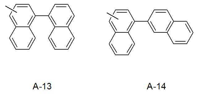


상기 화합물들에 있어서, 


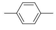


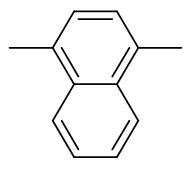
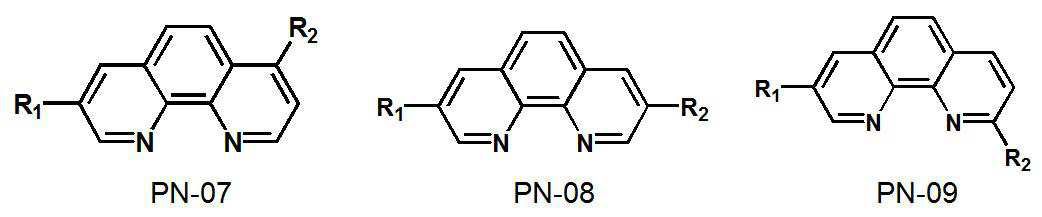
상기 화학식 2로 표시되는 페난쓰롤린 화합물은 하기 표시되는 화합물들 중에서 선택된 어느 하나인 것을 특징으로 한다.The phenanthroline compound represented by Chemical Formula 2 is characterized in that any one selected from the compounds represented below.




상기 발광층과 상기 P형 전하생성층 사이에 전자수송층을 더 포함하는 것을 특징으로 한다.It is characterized in that it further comprises an electron transport layer between the light emitting layer and the P-type charge generation layer.
상기 혼합층은 상기 전자수송층과 상기 P형 전하생성층 사이에 위치하며, 상기 트리아진 화합물들의 혼합 또는 상기 트리아진 화합물과 상기 페난쓰롤린 화합물의 혼합으로 이루어진 것을 특징으로 한다.The mixed layer is located between the electron transport layer and the P-type charge generation layer, and is characterized in that it consists of a mixture of the triazine compounds or a mixture of the triazine compound and the phenanthroline compound.
상기 혼합층은 전자수송층이며, 상기 트리아진 화합물들의 혼합 또는 상기 트리아진 화합물과 상기 페난쓰롤린 화합물의 혼합으로 이루어진 것을 특징으로 한다.The mixed layer is an electron transport layer, and is characterized in that it consists of a mixture of the triazine compounds or a mixture of the triazine compound and the phenanthroline compound.
상기 P형 전하생성층과 상기 전자수송층 사이에 위치하는 N형 전하생성층을 더 포함하는 것을 특징으로 한다.It is characterized in that it further comprises an N-type charge generation layer located between the P-type charge generation layer and the electron transport layer.
상기 혼합층은 상기 N형 전하생성층이며, 상기 페난쓰롤린 화합물들의 혼합 또는 상기 트리아진 화합물과 상기 페난쓰롤린 화합물의 혼합으로 이루어진 것을 특징으로 한다.The mixed layer is the N-type charge generation layer, and is characterized in that it is composed of a mixture of the phenanthroline compounds or a mixture of the triazine compound and the phenanthroline compound.
상기 혼합층은 상기 전자수송층과 상기 N형 전하생성층 사이에 위치하며, 상기 페난쓰롤린 화합물들의 혼합 또는 상기 트리아진 화합물과 상기 페난쓰롤린 화합물의 혼합으로 이루어진 것을 특징으로 한다.The mixed layer is located between the electron transport layer and the N-type charge generation layer, and is characterized in that it is composed of a mixture of the phenanthroline compounds or a mixture of the triazine compound and the phenanthroline compound.
상기 혼합층은 제1 혼합층 및 상기 제1 혼합층 상에 위치하는 제2 혼합층을 포함하며, 상기 제1 혼합층은 전자수송층이고 상기 제2 혼합층은 N형 전하생성층이고, 상기 제1 혼합층은 상기 트리아진 화합물들의 혼합 또는 상기 트리아진 화합물과 상기 페난쓰롤린 화합물의 혼합으로 이루어지며 상기 제2 혼합층은 상기 페난쓰롤린 화합물들의 혼합 또는 상기 트리아진 화합물과 상기 페난쓰롤린 화합물의 혼합으로 이루어진 것을 특징으로 한다.The mixed layer includes a first mixed layer and a second mixed layer disposed on the first mixed layer, the first mixed layer is an electron transport layer, the second mixed layer is an N-type charge generation layer, and the first mixed layer is the triazine. A mixture of compounds or a mixture of the triazine compound and the phenanthroline compound, and the second mixed layer is a mixture of the phenanthroline compounds or a mixture of the triazine compound and the phenanthroline compound. .
상기 혼합층은 상기 전자수송층과 상기 N형 전하생성층 사이에 위치하며, 상기 혼합층은 제1 혼합층 및 상기 제1 혼합층 상에 위치하는 제2 혼합층을 포함하고, 상기 제1 혼합층은 상기 트리아진 화합물들의 혼합 또는 상기 트리아진 화합물과 상기 페난쓰롤린 화합물의 혼합으로 이루어지며 상기 제2 혼합층은 상기 페난쓰롤린 화합물들의 혼합 또는 상기 트리아진 화합물과 상기 페난쓰롤린 화합물의 혼합으로 이루어진 것을 특징으로 한다.The mixed layer is located between the electron transport layer and the N-type charge generation layer, the mixed layer includes a first mixed layer and a second mixed layer disposed on the first mixed layer, and the first mixed layer is composed of the triazine compounds. It is characterized by mixing or mixing the triazine compound and the phenanthroline compound, and the second mixed layer is made of a mixture of the phenanthroline compounds or a mixture of the triazine compound and the phenanthroline compound.
본 발명의 트리아진 화합물은 전자가 풍부한 질소(N)를 3개 포함함으로써, 빠른 전자 이동도를 가져 전자의 수송을 용이하게 하고, 전자이동도가 상대적으로 빠른 치환기를 포함하여 혼합층에서 발광층으로의 전자의 수송을 용이하게 한다. 또한, 본 발명의 페난쓰롤린 화합물은 전자가 풍부한 질소(N)를 2개 포함함으로써, 빠른 전자 이동도를 가져 전자의 수송을 용이하게 한다. 특히, 페난쓰롤린 화합물은 전자가 상대적으로 풍부한 sp2 혼성 오비탈의 질소(N)를 포함하고, 이 질소가 N형 전하생성층의 도펀트인 알칼리금속 또는 알칼리 토금속과 결합(binding)하여 갭 스테이트(gap state)를 형성한다. 따라서, 형성된 갭 스테이트에 의해, N형 전하생성층에서 전자수송층으로 전자의 수송을 원활하게 할 수 있다. The triazine compound of the present invention contains three electron-rich nitrogen (N), thereby facilitating the transport of electrons by having fast electron mobility, and including a substituent having relatively fast electron mobility, so that it can move from the mixed layer to the light emitting layer. Facilitates the transport of electrons. In addition, since the phenanthroline compound of the present invention contains two electron-rich nitrogen (N), it has high electron mobility and facilitates electron transport. In particular, the phenanthroline compound contains nitrogen (N) of an sp2 hybrid orbital that is relatively rich in electrons, and this nitrogen is bound to an alkali metal or alkaline earth metal, which is a dopant of the N-type charge generation layer, to form a gap state (gap). state) is formed. Accordingly, electrons can be smoothly transported from the N-type charge generation layer to the electron transport layer by the formed gap state.
따라서, 본 발명의 유기발광소자는 발광층과 P형 전하생성층 사이에 혼합층을 구비하고, 혼합층에 2개 이상의 질소 원자를 포함하며 전자이동도가 상대적으로 빠른 치환기를 포함하는 화합물을 사용함으로써, N형 전하생성층으로부터 전달되는 전자를 발광층에 효율적으로 전달하여 소자의 효율 및 소자의 성능을 향상시킬 수 있다. 그리고 N형 전하생성층에서 전자수송층으로 전자의 전달이 원활해지므로 전자 주입이 원활하지 못해서 생기는 수명이 저하되는 문제점을 개선할 수 있다. 그리고 전자수송층과 N형 전하생성층 간의 LUMO 에너지 레벨 차이로 인해 N형 전하생성층으로 주입된 전자가 전자수송층으로 이동할 때 생기는 구동 전압이 상승되는 문제점을 개선할 수 있다. Therefore, the organic light emitting device of the present invention includes a mixed layer between the light emitting layer and the P-type charge generation layer, and uses a compound containing two or more nitrogen atoms in the mixed layer and a substituent having relatively fast electron mobility, so that N Efficiency and performance of the device may be improved by efficiently transferring electrons transferred from the type charge generation layer to the light emitting layer. In addition, since the transfer of electrons from the N-type charge generation layer to the electron transport layer is smooth, it is possible to improve the problem of reduced lifespan caused by poor electron injection. In addition, it is possible to improve a problem in which a driving voltage increases when electrons injected into the N-type charge generation layer move to the electron transport layer due to a difference in LUMO energy level between the electron transport layer and the N-type charge generation layer.
도 1 내지 도 6은 본 발명의 제1 실시예에 따른 유기발광소자를 나타낸 도면.
도 7 및 도 8은 본 발명의 제2 실시예에 따른 유기발광소자를 나타낸 도면.
도 9는 본 발명의 비교예 1과 2에 따라 제조된 소자의 구동전압에 따른 전류밀도를 나타낸 그래프.
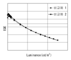
도 10은 본 발명의 비교예 1과 2에 따라 제조된 소자의 휘도에 따른 발광효율을 나타낸 그래프.
도 11은 본 발명의 비교예 1과 2에 따라 제조된 소자의 휘도에 따른 양자효율을 나타낸 그래프.
도 12는 본 발명의 비교예 1과 실시예 1에 따라 제조된 소자의 구동전압에 따른 전류밀도를 나타낸 그래프.
도 13은 본 발명의 비교예 1과 실시예 1에 따라 제조된 소자의 휘도에 따른 양자효율을 나타낸 그래프.
도 14는 본 발명의 비교예 1과 실시예 2에 따라 제조된 소자의 구동전압에 따른 전류밀도를 나타낸 그래프.
도 15는 본 발명의 비교예 1과 실시예 2에 따라 제조된 소자의 휘도에 따른 양자효율을 나타낸 그래프.
도 16은 본 발명의 비교예 1과 실시예 3에 따라 제조된 소자의 구동전압에 따른 전류밀도를 나타낸 그래프.
도 17은 본 발명의 비교예 1과 실시예 3에 따라 제조된 소자의 휘도에 따른 양자효율을 나타낸 그래프.
도 18은 본 발명의 비교예 1과 실시예 4에 따라 제조된 소자의 구동전압에 따른 전류밀도를 나타낸 그래프.
도 19는 본 발명의 비교예 1과 실시예 4에 따라 제조된 소자의 휘도에 따른 양자효율을 나타낸 그래프.
도 20은 본 발명의 비교예 1, 실시예 5 및 실시예 6에 따라 제조된 소자의 구동전압에 따른 전류밀도를 나타낸 그래프.
도 21은 본 발명의 비교예 1, 실시예 5 및 실시예 6에 따라 제조된 소자의 휘도에 따른 양자효율을 나타낸 그래프.
도 22는 본 발명의 비교예 1과 실시예 7에 따라 제조된 소자의 구동전압에 따른 전류밀도를 나타낸 그래프.
도 23은 본 발명의 비교예 1과 실시예 7에 따라 제조된 소자의 휘도에 따른 양자효율을 나타낸 그래프.1 to 6 are views illustrating an organic light emitting device according to a first embodiment of the present invention.
7 and 8 are views illustrating an organic light emitting device according to a second embodiment of the present invention.
9 is a graph showing the current density according to the driving voltage of the devices manufactured according to Comparative Examples 1 and 2 of the present invention.
10 is a graph showing the luminous efficiency according to the luminance of the devices manufactured according to Comparative Examples 1 and 2 of the present invention.
11 is a graph showing quantum efficiency according to luminance of devices manufactured according to Comparative Examples 1 and 2 of the present invention.
12 is a graph showing the current density according to the driving voltage of the devices manufactured according to Comparative Example 1 and Example 1 of the present invention.
13 is a graph showing quantum efficiency according to luminance of devices manufactured according to Comparative Example 1 and Example 1 of the present invention.
14 is a graph showing the current density according to the driving voltage of the devices manufactured according to Comparative Example 1 and Example 2 of the present invention.
15 is a graph showing quantum efficiency according to luminance of devices manufactured according to Comparative Example 1 and Example 2 of the present invention.
16 is a graph showing the current density according to the driving voltage of the devices manufactured according to Comparative Example 1 and Example 3 of the present invention.
17 is a graph showing quantum efficiency according to luminance of devices manufactured according to Comparative Example 1 and Example 3 of the present invention.
18 is a graph showing the current density according to the driving voltage of the devices manufactured according to Comparative Example 1 and Example 4 of the present invention.
19 is a graph showing quantum efficiency according to luminance of devices manufactured according to Comparative Example 1 and Example 4 of the present invention.
20 is a graph showing the current density according to the driving voltage of the devices manufactured according to Comparative Example 1, Example 5 and Example 6 of the present invention.
21 is a graph showing quantum efficiency according to luminance of devices manufactured according to Comparative Example 1, Example 5, and Example 6 of the present invention.
22 is a graph showing the current density according to the driving voltage of the devices manufactured according to Comparative Example 1 and Example 7 of the present invention.
23 is a graph showing quantum efficiency according to luminance of devices manufactured according to Comparative Example 1 and Example 7 of the present invention.
본 발명의 이점 및 특징, 그리고 그것들을 달성하는 방법은 첨부되는 도면과 함께 상세하게 후술되어 있는 실시예들을 참조하면 명확해질 것이다. 그러나 본 발명은 이하에서 개시되는 실시예들에 한정되는 것이 아니라 서로 다른 다양한 형태로 구현될 것이며, 단지 본 실시예들은 본 발명의 개시가 완전하도록 하며, 본 발명이 속하는 기술 분야에서 통상의 지식을 가진 자에게 발명의 범주를 완전하게 알려주기 위해 제공되는 것이며, 본 발명은 청구항의 범주에 의해 정의될 뿐이다. Advantages and features of the present invention, and methods of achieving them, will become clear with reference to the detailed description of the following embodiments taken in conjunction with the accompanying drawings. However, the present invention is not limited to the embodiments disclosed below, but will be implemented in a variety of different forms, and only the present embodiments make the disclosure of the present invention complete, and common knowledge in the art to which the present invention belongs. It is provided to fully inform the holder of the scope of the invention, and the present invention is only defined by the scope of the claims.
본 발명의 실시예를 설명하기 위한 도면에 개시된 형상, 크기, 비율, 각도, 개수 등은 예시적인 것이므로 본 발명이 도시된 사항에 한정되는 것은 아니다. 명세서 전체에 걸쳐 동일 참조 부호는 동일 구성 요소를 지칭한다. 또한, 본 발명을 설명함에 있어서, 관련된 공지 기술에 대한 구체적인 설명이 본 발명의 요지를 불필요하게 흐릴 수 있다고 판단되는 경우 그 상세한 설명은 생략한다. 본 명세서 상에서 언급한 '포함한다', '갖는다', '이루어진다' 등이 사용되는 경우 '~만'이 사용되지 않는 이상 다른 부분이 추가될 수 있다. 구성 요소를 단수로 표현한 경우에 특별히 명시적인 기재 사항이 없는 한 복수를 포함하는 경우를 포함한다.The shapes, sizes, ratios, angles, numbers, etc. disclosed in the drawings for explaining the embodiments of the present invention are illustrative, so the present invention is not limited to the details shown. Like reference numbers designate like elements throughout the specification. In addition, in describing the present invention, if it is determined that a detailed description of related known technologies may unnecessarily obscure the subject matter of the present invention, the detailed description will be omitted. When 'includes', 'has', 'consists of', etc. mentioned in this specification is used, other parts may be added unless 'only' is used. In the case where a component is expressed in the singular, the case including the plural is included unless otherwise explicitly stated.
구성 요소를 해석함에 있어서, 별도의 명시적 기재가 없더라도 오차 범위를 포함하는 것으로 해석한다.In interpreting the components, even if there is no separate explicit description, it is interpreted as including the error range.
위치 관계에 대한 설명일 경우, 예를 들어, '~상에', '~상부에', '~하부에', '~옆에' 등으로 두 부분의 위치 관계가 설명되는 경우, '바로' 또는 '직접'이 사용되지 않는 이상 두 부분 사이에 하나 이상의 다른 부분이 위치할 수도 있다.In the case of a description of a positional relationship, for example, 'on top of', 'on top of', 'at the bottom of', 'next to', etc. Or, unless 'directly' is used, one or more other parts may be located between the two parts.
시간 관계에 대한 설명일 경우, 예를 들어, '~후에', '~에 이어서', '~다음에', '~전에' 등으로 시간적 선후 관계가 설명되는 경우, '바로' 또는 '직접'이 사용되지 않는 이상 연속적이지 않은 경우도 포함할 수 있다.In the case of a description of a temporal relationship, for example, 'immediately' or 'directly' when a temporal precedence relationship is described in terms of 'after', 'following', 'next to', 'before', etc. It can also include non-continuous cases unless is used.
제1, 제2 등이 다양한 구성요소들을 서술하기 위해서 사용되나, 이들 구성요소들은 이들 용어에 의해 제한되지 않는다. 이들 용어들은 단지 하나의 구성 요소를 다른 구성요소와 구별하기 위하여 사용하는 것이다. 따라서, 이하에서 언급되는 제1 구성요소는 본 발명의 기술적 사상 내에서 제2 구성요소일 수도 있다.Although first, second, etc. are used to describe various components, these components are not limited by these terms. These terms are only used to distinguish one component from another. Therefore, the first component mentioned below may also be the second component within the technical spirit of the present invention.
본 발명의 여러 실시예들의 각각 특징들이 부분적으로 또는 전체적으로 서로 결합 또는 조합 가능하고, 기술적으로 다양한 연동 및 구동이 가능하며, 각 실시예들이 서로에 대하여 독립적으로 실시 가능할 수도 있고 연관 관계로 함께 실시할 수도 있다.Each feature of the various embodiments of the present invention can be partially or entirely combined or combined with each other, technically various interlocking and driving are possible, and each embodiment can be implemented independently of each other or can be implemented together in a related relationship. may be
이하, 첨부된 도면을 참조하여 본 발명의 다양한 실시 예들을 자세하게 설명하면 다음과 같다. Hereinafter, various embodiments of the present invention will be described in detail with reference to the accompanying drawings.
<제1 실시예><First Embodiment>
도 1 내지 도 6은 본 발명의 제1 실시예에 따른 유기발광소자를 나타낸 도면이다.1 to 6 are views showing an organic light emitting device according to a first embodiment of the present invention.
도 1을 참조하면, 본 발명의 유기발광소자(100)는 양극(110)과 음극(220) 사이에 위치하는 발광부들(ST1, ST2) 및 발광부들(ST1, ST2) 사이에 위치하는 전하생성층(160)을 포함한다. 상기 제1 발광부(ST1)는 하나의 발광소자 단위를 이루는 것으로, 제1 정공주입층(120), 제1 정공수송층(130), 제1 발광층(140), 제1 전자수송층(150), 혼합층(300)을 포함한다. Referring to FIG. 1, the organic
양극(110)은 정공을 주입하는 전극으로 일함수가 높은 ITO(Indium Tin Oxide), IZO(Indium Zinc Oxide) 또는 ZnO(Zinc Oxide) 중 어느 하나일 수 있다. 또한, 상기 양극(110)이 반사 전극일 경우에 양극(110)은 ITO, IZO 또는 ZnO 중 어느 하나로 이루어진 층 하부에 알루미늄(Al), 은(Ag) 또는 니켈(Ni) 중 어느 하나로 이루어진 반사층을 더 포함할 수 있다.The
제1 정공주입층(120)은 양극(110)으로부터 제1 발광층(140)으로 정공의 주입을 원활하게 하는 역할을 할 수 있으며, CuPc(cupper phthalocyanine), PEDOT(poly(3,4)-ethylenedioxythiophene), PANI(polyaniline) 및 NPD(N,N'-bis(naphthalen-1-yl)-N,N'-bis(phenyl)-2,2'-dimethylbenzidine)로 이루어진 군에서 선택된 어느 하나 이상으로 이루어질 수 있으나 이에 한정되지 않는다. 상기 제1 정공주입층(120)의 두께는 1 내지 150nm일 수 있다. 여기서, 상기 제1 정공주입층(120)의 두께가 1nm 이상이면 정공 주입 특성을 향상시킬 수 있고, 150nm 이하이면 제1 정공주입층(120)의 두께의 증가를 최소화하여 구동 전압의 상승을 최소화할 수 있다. 상기 제1 정공주입층(120)은 소자의 구조나 특성에 따라 유기발광소자의 구성에 포함되지 않을 수도 있다.The first
상기 제1 정공수송층(130)은 정공의 수송을 원활하게 하는 역할을 하며, NPD(N,N'-bis(naphthalen-1-yl)-N,N'-bis(phenyl)-2,2'-dimethylbenzidine), TPD(N,N'-bis(3-methylphenyl)-N,N'-bis-(phenyl)-benzidine), spiro-TAD(2,2',7,7'-tetrakis(N,N-diphenylamino)-9,9'-spirofluorene) 및 MTDATA(4,4',4"-Tris(N-3-methylphenyl-N-phenylamino)-triphenylamine)로 이루어진 군에서 선택된 어느 하나 이상으로 이루어질 수 있으나 이에 한정되지 않는다. 상기 제1 정공수송층(130)의 두께는 1 내지 150nm일 수 있다. 여기서, 상기 제1 정공수송층(130)의 두께가 1nm 이상이면 정공 수송 특성을 향상시킬 수 있고, 150nm 이하이면 제1 정공수송층(130)의 두께의 증가를 최소화하여 구동 전압의 상승을 최소화할 수 있다.The first
상기 제1 발광층(140)은 적색, 녹색 및 청색 중 하나의 색을 발광할 수 있으며, 본 실시예에서는 청색 발광층일 수 있다. 청색 발광층인 경우 제1 발광층(140)은 CBP(4,4'-bis(carbazol-9-yl)biphenyl) 등의 호스트 물질을 포함하며, 이리듐(iridium) 계열을 포함하는 도펀트 물질을 포함하는 인광물질로 이루어질 수 있으나, 이에 한정되지 않는다. 또는, spiro-DPVBi, spiro-CBP, 디스틸벤젠(DSB), 디스트릴아릴렌(DSA), PFO계 고분자 및 PPV계 고분자로 이루어진 군에서 선택된 어느 하나를 포함하는 형광물질로 이루어질 수 있으나 이에 한정되지 않는다. 여기서 청색 발광층은 청색(Blue) 발광층, 진청색(Dark Blue) 발광층 또는 스카이 블루(Sky Blue) 발광층 중 하나를 포함한다.The first light-emitting
상기 제1 전자수송층(150)은 전자의 수송을 원활하게 하는 역할을 하며, Alq3(tris(8-hydroxy-quinolinato)aluminum), PBD(2-(4-biphenyl)-5-(4-tert-butylphenyl)-1,3,4-oxadiazole), TAZ(3-(4-biphenyl)-4-phenyl-5-tert-butylphenyl-1,2,4-triazole), DPT(2-biphenyl-4-yl-4,6-bis-(4 ′-pyridin-2-yl-biphenyl-4-yl)-[1,3,5]triazine) 및 BAlq(Bis(2-methyl-8-quinolinolate)-4-(phenylphenolato)aluminum)로 이루어진 군에서 선택된 어느 하나 이상으로 이루어질 수 있으나 이에 한정되지 않는다. 제1 전자수송층(150)의 두께는 1 내지 150nm일 수 있다. 여기서, 제1 전자수송층(150)의 두께가 1nm 이상이면 전자 수송 특성이 저하되는 것을 최소화할 수 있는 이점이 있고, 150nm 이하이면 제1 전자수송층(150)의 두께의 증가를 최소화하여 구동 전압의 상승을 최소화할 수 있다. The first
제1 발광부(ST1) 상에 전하생성층(Charge Generation Layer; CGL)(160)이 위치한다. 상기 제1 발광부(ST1)와 상기 제2 발광부(ST2)는 상기 전하생성층(160)에 의해 연결된 구조로 이루어져 있다. 상기 전하생성층(160)은 N형 전하생성층(160N)과 P형 전하생성층(160P)이 접합된 PN접합 전하생성층일 수 있다. 이때, 상기 PN접합 전하생성층(160)은 전하를 생성하거나 정공 및 전자로 분리하여 상기 각 발광층에 전하를 주입한다. 즉, N형 전하생성층(160N)은 양극에 인접한 제1 발광층(140)에 전자를 공급하고, 상기 P형 전하생성층(160P)은 제2 발광부(ST2)의 발광층에 정공을 공급함으로써, 다수의 발광층을 구비하는 유기발광소자의 발광 효율을 더욱 증대시킬 수 있으며, 구동 전압도 낮출 수 있다. 따라서, 상기 전하생성층(160)은 유기발광소자의 특성인 발광 효율이나 구동 전압에 중요한 영향을 미치게 된다. A charge generation layer (CGL) 160 is positioned on the first light emitting part ST1. The first light emitting part ST1 and the second light emitting part ST2 have a structure connected by the
N형 전하생성층(160N)은 금속 또는 N형이 도핑된 유기물질로 이루어질 수 있다. 여기서, 상기 금속은 Li, Na, K, Rb, Cs, Mg, Ca, Sr, Ba, La, Ce, Sm, Eu, Tb, Dy 및 Yb로 이루어진 군에서 선택된 하나의 물질일 수 있다. 또한, 상기 N형이 도핑된 유기물질에 사용되는 N형 도펀트와 호스트의 물질은 통상적으로 사용되는 물질을 이용할 수 있다. 예를 들면, 상기 N형 도펀트는 알칼리 금속, 알칼리 금속 화합물, 알칼리 토금속 또는 알칼리 토금속 화합물일 수 있다. 자세하게는 상기 N형 도펀트는 Li, Cs, K, Rb, Mg, Na, Ca, Sr, Eu 및 Yb로 이루어진 군에서 선택된 하나일 수 있다. 도펀트의 비율은 호스트 전체 100% 대비 1 내지 10%로 혼합된다. 여기서, 도펀트의 일함수(work function)는 2.5eV 이상인 것이 바람직하다. 상기 호스트 물질은 질소 원자를 포함하는 헤테로고리를 갖는 탄소수가 20개 이상 60개 이하인 유기물일 수 있고, 예를 들어, Alq3(tris(8-hydroxy-quinolinato)aluminum), 페난쓰롤린(phenanthroline) 유도체, 하이드록시퀴놀린(hydroxy quinoline) 유도체 및 벤즈아졸(benzazole) 유도체 및 실롤(silole) 유도체로 이루어진 군에서 선택된 하나의 물질일 수 있다.The N-type
P형 전하생성층(160P)은 금속 또는 P형이 도핑된 유기물질로 이루어질 수 있다. 여기서, 상기 금속은 Al, Cu, Fe, Pb, Zn, Au, Pt, W, In, Mo, Ni 및 Ti로 이루어진 군에서 선택된 하나 또는 둘이상의 합금으로 이루어질 수 있다. 또한, 상기 P형이 도핑된 유기물질에 사용되는 P형 도펀트와 호스트의 물질은 통상적으로 사용되는 물질을 이용할 수 있다. 예를 들면, 상기 P형 도펀트는 F4-TCNQ(2,3,5,6-tetrafluoro-7,7,8,8-tetracyano-quinodimethane) 등의 테트라시아노퀴노디메탄의 유도체, 요오드, FeCl3, FeF3 및 SbCl5으로 이루어진 군에서 선택된 하나의 물질일 수 있다. 또한, 상기 호스트는 NPB(N,N’-bis(naphthaen-1-yl)-N,N’-bis(phenyl)-benzidine), TPD(N,N’-bis(3-methylphenyl)N,N’-bis(phenyl)-benzidine) 및 TNB(N,N,N’,N’-tetra-naphthalenyl-benzidine)로 이루어진 군에서 선택된 하나의 물질일 수 있다.The P-type
상기 전하생성층(160) 상에 제2 정공주입층(170), 제2 정공수송층(180), 제2 발광층(190), 제2 전자수송층(200) 및 전자주입층(210)을 포함하는 제2 발광부(ST2)가 위치한다. 제2 정공주입층(170), 제2 정공수송층(180) 및 제2 전자수송층(200)은 전술한 제1 발광부(ST1)의 제1 정공주입층(120), 제1 정공수송층(130) 및 제1 전자수송층(150)의 구성과 각각 동일하거나 다르게 이루어질 수 있다. 동일한 구성에 대해서는 자세한 설명을 생략하기로 한다.A second
제2 발광층(190)은 적색, 녹색, 청색 등의 하나의 색을 발광하는 발광층으로 본 실시예에서는 노란색 발광층일 수 있다. 제2 발광층(190)이 노란색 발광층인 경우 옐로그린(Yellow-Green)을 발광하는 발광층 또는 그린(Green)을 발광하는 발광층의 단층 구조 또는 옐로그린 발광층과 그린(Green)을 발광하는 발광층의 다층 구조로 이루어질 수 있다. 여기서 제2 발광층(190)은 옐로그린(Yellow-Green) 발광층 또는 그린(Green)을 발광하는 발광층 또는 옐로그린 발광층과 그린(Green)을 발광하는 발광층의 다층 구조를 포함한다. 본 실시예에서는 옐로그린을 발광하는 노란색 발광층의 단층 구조를 예로 설명한다. 제2 발광층(190)은 CBP(4,4'-bis(carbazol-9-yl)biphenyl) 또는 BAlq(Bis(2-methyl-8-quinolinolate)-4-(phenylphenolato)aluminium) 중 선택된 적어도 하나의 호스트에 옐로그린을 발광하는 인광 옐로그린 도펀트로 이루어질 수 있다. 그러나 이에 한정되는 것은 아니다.The second light-emitting
상기 전자주입층(210)은 전자의 수송을 원활하게 하는 역할을 하며, Alq3(tris(8-hydroxy-quinolinato)aluminum), PBD(2-(4-biphenyl)-5-(4-tert-butylphenyl)-1,3,4-oxadiazole), TAZ(3-(4-biphenyl)-4-phenyl-5-tert-butylphenyl-1,2,4-triazole), 및 BAlq(Bis(2-methyl-8-quinolinolate)-4-(phenylphenolato)aluminum)를 사용할 수 있으나 이에 한정되지 않는다. 반면, 전자주입층(210)은 금속화합물로 이루어질 수 있으며, 금속화합물은 예를 들어 LiQ, LiF, NaF, KF, RbF, CsF, FrF, BeF2, MgF2, CaF2, SrF2, BaF2 및 RaF2로 이루어진 군에서 선택된 어느 하나 이상일 수 있으나 이에 한정되지 않는다. 상기 전자주입층(210)의 두께는 1 내지 50nm일 수 있다. 여기서, 상기 전자주입층(210)의 두께가 1nm 이상이면, 전자 주입 특성이 저하되는 것을 최소화할 수 있는 이점이 있고, 50nm 이하이면 전자주입층(210)의 두께의 증가를 최소화하여 구동 전압의 상승을 최소화할 수 있다. 따라서, 전하생성층(160) 상에 제2 정공주입층(170), 제2 정공수송층(180), 제2 발광층(190), 제2 전자수송층(200) 및 전자주입층(210)을 포함하는 제2 발광부(ST2)를 구성한다. The
제2 발광부(ST2) 상에는 음극(220)이 위치한다. 상기 음극(220)은 전자 주입 전극으로, 일함수가 낮은 마그네슘(Mg), 칼슘(Ca), 알루미늄(Al), 은(Ag) 또는 이들의 합금으로 이루어질 수 있다. 여기서, 음극(220)은 유기발광소자가 전면 또는 양면발광구조일 경우, 빛을 투과할 수 있을 정도로 얇은 두께로 형성할 수 있으며, 유기발광소자가 배면발광구조일 경우, 빛을 반사시킬 수 있을 정도로 두껍게 형성할 수 있다. A
한편, 본 발명은 제1 발광부(ST1)에 혼합층(300)을 포함한다. 혼합층(300)은 제1 전자수송층(150)과 N형 전하생성층(160N) 사이에 위치하여, N형 전하생성층(160N)에서 제1 전자수송층(150)으로의 전자의 수송을 원활하게 하는 역할을 한다. Meanwhile, in the present invention, the
본 발명은 N형 전하생성층(160N)에서 제1 전자수송층(150)으로의 전자 주입 특성을 향상시키기 위한 여러 실험을 하게 되었다. 이 실험을 통하여 전자수송층과 N형 전하생성층 간의 LUMO 에너지 레벨 차이로 인해 N형 전하생성층으로 주입된 전자가 전자수송층으로 이동할 때 구동 전압이 상승함을 인식하였다. 따라서, 구동 전압이 감소되고 효율이 향상될 수 있도록 제1 전자수송층(150)과 N형 전하생성층(160N) 사이에 혼합층(300)을 형성하였다. 특히, 본 발명은 소자의 구동 전압의 상승을 최소화하고 효율을 향상시킬 수 있도록 여러 실험을 통하여 트리아진 화합물들의 혼합 또는 트리아진 화합물과 페난쓰롤린 화합물이 혼합된 혼합층(300)을 도입하였다. In the present invention, various experiments have been conducted to improve electron injection characteristics from the N-type
본 발명의 트리아진 화합물은 전자가 풍부한 질소(N)를 3개 포함함으로써, 빠른 전자 이동도를 가져 전자의 수송을 용이하게 한다. 또한, 트리아진 화합물은 전자이동도가 상대적으로 빠른 치환기를 포함하여, 혼합층에서 발광층으로의 전자의 수송을 용이하게 한다.The triazine compound of the present invention contains three electron-rich nitrogen (N), thereby facilitating the transport of electrons due to high electron mobility. In addition, the triazine compound includes a substituent having a relatively high electron mobility, thereby facilitating electron transport from the mixed layer to the light emitting layer.
본 발명의 실시예에서 혼합층(300)에 사용되는 트리아진 화합물은 하기 화학식 1로 표시된다. In an embodiment of the present invention, the triazine compound used in the
[화학식 1][Formula 1]

상기 화학식 1에서, X1 내지 X10은 각각 독립적으로 CH 또는 C(R1) 또는 C(R2)이며, R1 과 R2는 각각 독립적으로 탄소수 6 내지 50의 방향족 고리화합물 중에서 선택되거나 N, S, O 또는 Si 원자가 1개 이상 포함되고 탄소수 5 내지 50의 이형 고리화합물 중에서 선택되고, 상기 C(R1)이나 C(R2)는 각각 같은 고리 내에 존재하거나 존재하지 않는다. In Formula 1, X 1 to X 10 are each independently CH or C(R 1 ) or C(R 2 ), and R 1 and R 2 are each independently selected from aromatic ring compounds having 6 to 50 carbon atoms or N , It is selected from heterocyclic compounds containing one or more S, O or Si atoms and having 5 to 50 carbon atoms, and the C(R 1 ) or C(R 2 ) is present or absent in the same ring, respectively.
또한, 화학식 1로 표시되는 트리아진 화합물은 하기 표시되는 화합물들 중에서 선택된 어느 하나로 이루어진다. In addition, the triazine compound represented by Formula 1 consists of any one selected from the compounds represented below.


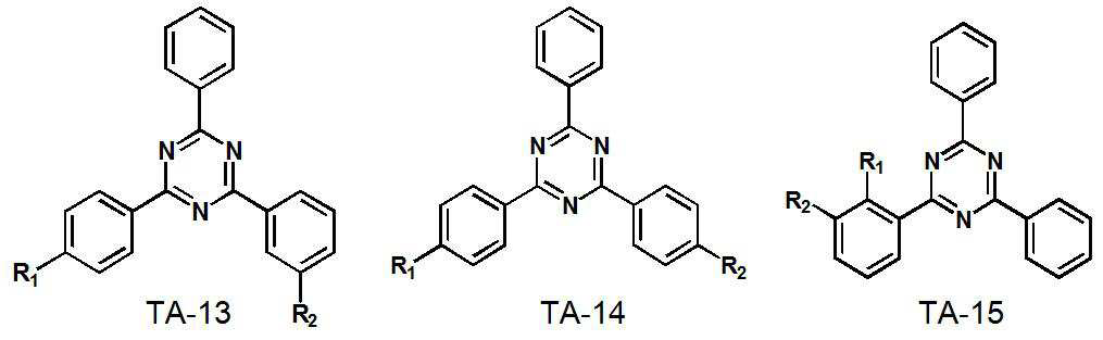


상기 화합물들 중에서 R1 및 R2는 각각 독립적으로 수소, 중수소, 할로겐원자, 하이드록실기, 시아노기, 니트로기, 아미노기, 아미디노기, 히드라진, 히드라존, 카르복실기나 이의 염, 술폰산기나 이의 염, 인산기나 이의 염, 치환 또는 비치환된 탄소수 1 내지 60의 알킬기, 치환 또는 비치환된 탄소수 2 내지 60의 알케닐기, 치환 또는 비치환된 탄소수 2 내지 60의 알키닐기, 치환 또는 비치환된 탄소수 1 내지 60의 알콕시기, 치환 또는 비치환된 탄소수 3 내지 60의 시클로 알킬기, 치환 또는 비치환된 탄소수 6 내지 60의 아릴기, 치환 또는 비치환된 아릴옥시기, 치환 또는 비치환된 탄소수 6 내지 60의 아릴싸이오기, 치환 또는 비치환된 탄소수 2 내지 60의 헤테로아릴기 중 선택된 어느 하나이다.Among the above compounds, R 1 and R 2 are each independently hydrogen, deuterium, halogen atom, hydroxyl group, cyano group, nitro group, amino group, amidino group, hydrazine, hydrazone, carboxyl group or its salt, sulfonic acid group or its salt , A phosphoric acid group or a salt thereof, a substituted or unsubstituted alkyl group having 1 to 60 carbon atoms, a substituted or unsubstituted alkenyl group having 2 to 60 carbon atoms, a substituted or unsubstituted alkynyl group having 2 to 60 carbon atoms, a substituted or unsubstituted carbon number 1 to 60 alkoxy group, substituted or unsubstituted cycloalkyl group having 3 to 60 carbon atoms, substituted or unsubstituted aryl group having 6 to 60 carbon atoms, substituted or unsubstituted aryloxy group, substituted or unsubstituted 6 to 60 carbon atoms It is any one selected from a 60 arylthio group and a substituted or unsubstituted heteroaryl group having 2 to 60 carbon atoms.
구체적으로, R1 및 R2는 각각 독립적으로 하기 표시되는 화합물들 중에서 선택된 어느 하나로 이루어진다.Specifically, R 1 and R 2 each independently consist of any one selected from compounds shown below.


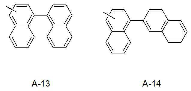


상기 화합물들에 있어서, 


또한, 본 발명의 페난쓰롤린 화합물은 전자가 풍부한 질소(N)를 2개 포함함으로써, 빠른 전자 이동도를 가져 전자의 수송을 용이하게 한다. 또한, 페난쓰롤린 화합물은 전자이동도가 상대적으로 빠른 치환기를 포함하여, 혼합층에서 발광층으로의 전자의 수송을 용이하게 한다.In addition, since the phenanthroline compound of the present invention contains two electron-rich nitrogen (N), it has high electron mobility and facilitates electron transport. In addition, the phenanthroline compound includes a substituent having relatively high electron mobility, thereby facilitating electron transport from the mixed layer to the light emitting layer.
본 발명의 실시예에서 혼합층(300)에 사용되는 페난쓰롤린 화합물은 하기 화학식 2로 표시된다. In an embodiment of the present invention, the phenanthroline compound used in the
[화학식 2][Formula 2]
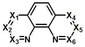
상기 화학식 2에서, X1 내지 X6은 각각 독립적으로 CH 또는 C(R1) 또는 C(R2)이며, R1 과 R2는 각각 독립적으로 탄소수 6 내지 50의 방향족 고리화합물 중에서 선택되거나 N, S, O 또는 Si 원자가 1개 이상 포함되고 탄소수 5 내지 50의 이형 고리화합물 중에서 선택되고, 상기 C(R1)이나 C(R2)는 각각 같은 고리 내에 존재하거나 존재하지 않는다. In Formula 2, X 1 to X 6 are each independently CH or C(R 1 ) or C(R 2 ), and R 1 and R 2 are each independently selected from aromatic ring compounds having 6 to 50 carbon atoms or N , It is selected from heterocyclic compounds containing one or more S, O or Si atoms and having 5 to 50 carbon atoms, and the C(R 1 ) or C(R 2 ) is present or absent in the same ring, respectively.
화학식 2로 표시되는 페난쓰롤린 화합물은 하기 표시되는 화합물들 중에서 선택된 어느 하나로 이루어진다.The phenanthroline compound represented by Formula 2 consists of any one selected from the compounds shown below.


여기서, 상기 R1과 R2는 전술한 트리아진 화합물의 R1과 R2와 동일하므로 그 설명을 생략한다.Here, since R 1 and R 2 are the same as R 1 and R 2 of the triazine compound described above, their descriptions are omitted.
본 발명의 혼합층(300)은 제1 전자수송층(150)과 N형 전하생성층(160N) 사이에 위치하여, 혼합 전자수송층 또는 혼합 N형 전하생성층으로 작용한다. 혼합 전자수송층은 화합물들이 혼합되되 전자 수송 특성이 우수한 혼합층이고, 혼합 N형 전하생성층은 화합물들이 혼합되되 전하 생성 특성이 우수한 혼합층이다. The
본 발명의 혼합층(300)은 트리아진 화합물들끼리의 혼합으로 이루어지거나 트리아진 화합물과 페난쓰롤린 화합물의 혼합으로 이루어져 혼합 전자수송층으로 작용할 수 있다. 또한, 본 발명의 혼합층(300)은 페난쓰롤린 화합물들끼리의 혼합으로 이루어지거나 트리아진 화합물과 페난쓰롤린 화합물의 혼합으로 이루어져 혼합 N형 전하생성층으로 작용할 수 있다. 여기서, 혼합층(300)이 혼합 N형 전하생성층으로 작용하는 경우, 혼합층(300)은 금속 또는 N형이 도핑된 유기물질로 이루어질 수 있다. 여기서, 상기 금속은 Li, Na, K, Rb, Cs, Mg, Ca, Sr, Ba, La, Ce, Sm, Eu, Tb, Dy 및 Yb로 이루어진 군에서 선택된 하나의 물질일 수 있다. 또한, 상기 N형이 도핑된 유기물질에 사용되는 N형 도펀트는 알칼리 금속, 알칼리 금속 화합물, 알칼리 토금속 또는 알칼리 토금속 화합물일 수 있다. 자세하게는 상기 N형 도펀트는 Li, Cs, K, Rb, Mg, Na, Ca, Sr, Eu 및 Yb로 이루어진 군에서 선택된 하나일 수 있다. 도펀트의 비율은 호스트 전체 100% 대비 1 내지 10%로 혼합된다. 여기서, 도펀트의 일함수(work function)는 2.5eV 이상인 것이 바람직하다. The
본 발명의 트리아진 화합물은 전하 생성 특성보다 전자 수송 특성이 더 우수하고, 페난쓰롤린 화합물은 전자 수송 특성보다 전하 생성 특성이 우수하다. 따라서, 본 발명의 혼합 전자수송층으로 작용하는 혼합층(300)의 경우는 적어도 트리아진 화합물이 포함되어 형성되고, 혼합 N형 전하생성층으로 작용하는 혼합층(300)의 경우는 적어도 페난쓰롤린 화합물이 포함되어 형성된다. The triazine compound of the present invention has better electron transport properties than charge generation properties, and the phenanthroline compound has better charge generation properties than electron transport properties. Therefore, in the case of the
한편, 혼합층(300)의 두께는 10 내지 600Å으로 이루어진다. 혼합층(300)의 두께가 10Å 이상이면 전자의 수송 특성을 향상시킬 수 있고, 600Å 이하이면 혼합층(300)의 두께의 증가를 최소화하여 구동 전압의 상승을 최소화할 수 있다. 또한, 혼합층(300)은 혼합된 화합물들이 일정 혼합비를 가지도록 형성된다. 예를 들어, 혼합층(300)은 혼합된 화합물들이 동일한 혼합비로 이루어지거나 서로 다른 혼합비로 이루어질 수 있다. 따라서 혼합층(300)의 혼합비는 0.1 : 99.9vol% 내지 99.9 : 0.1vol%로 이루어진다. 여기서 혼합층(300)의 혼합비가 0.1 : 99.9vol% 이상이면 혼합된 재료들의 전자 수송 특성을 극대화할 수 있고, 99.9 : 0.1vol% 이하이면 어느 하나의 재료의 특성이 약화되는 것을 최소화할 수 있다.Meanwhile, the
상기와 같이, 본 발명은 전자수송층과 N형 전하생성층 사이에 혼합 전자수송층 또는 혼합 N형 전하생성층으로 작용하는 혼합층을 형성하되 트리아진 화합물들의 혼합, 트리아진 화합물과 페난쓰롤린 화합물의 혼합 또는 페난쓰롤린 화합물들의 혼합으로 형성함으로써, N형 전하생성층으로부터 전자수송층으로 전달되는 전자의 수송을 원활하게 한다.As described above, the present invention forms a mixed layer acting as a mixed electron transport layer or a mixed N-type charge generation layer between the electron transport layer and the N-type charge generation layer, but a mixture of triazine compounds, a mixture of a triazine compound and a phenanthroline compound Or by forming a mixture of phenanthroline compounds, the transport of electrons transferred from the N-type charge generation layer to the electron transport layer is facilitated.
한편 본 발명의 제1 실시예에 따른 유기발광소자는 전술한 도 1의 구조와는 달리 발광층과 N형 전하생성층 사이에 전자수송층을 대신하는 혼합층(300)이 구비될 수도 있다.Meanwhile, unlike the structure of FIG. 1 described above, the organic light emitting device according to the first embodiment of the present invention may include a
도 2를 참조하면, 본 발명의 혼합층(300)은 제1 발광층(140)과 N형 전하생성층(160N) 사이에 위치한다. 여기서 혼합층(300)은 전자수송층의 역할을 하는 것으로, N형 전하생성층(160N)으로부터 제1 발광층(140)으로 전자를 용이하게 수송한다. 본 발명의 혼합층(300)이 전자수송층의 역할을 하는 경우, 혼합층(300)은 트리아진 화합물들의 혼합 또는 트리아진 화합물과 페난쓰롤린 화합물의 혼합으로 이루어진다. 전술한 바와 같이, 트리아진 화합물은 전자 수송 특성이 우수하기 때문에 전자수송층 대신에 혼합층이 사용되어도 전자수송층의 역할을 충분히 수행할 수 있다.Referring to FIG. 2 , the
한편 본 발명의 제1 실시예에 따른 유기발광소자는 전술한 도 1 및 도 2의 구조와는 달리 전자수송층과 P형 전하생성층 사이에 N형 전하생성층을 대신하는 혼합층(300)이 구비될 수도 있다.Meanwhile, unlike the structure of FIGS. 1 and 2 described above, the organic light emitting device according to the first embodiment of the present invention includes a
도 3을 참조하면, 본 발명의 혼합층(300)은 전자수송층(150)과 P형 전하생성층(160P) 사이에 위치한다. 여기서 혼합층(300)은 N형 전하생성층의 역할을 하는 것으로, 전자를 생성하여 제1 전자수송층(150)으로 전자를 수송한다. 본 발명의 혼합층(300)이 N형 전하생성층의 역할을 하는 경우, 혼합층(300)은 페난쓰롤린 화합물들의 혼합 또는 트리아진 화합물과 페난쓰롤린 화합물의 혼합으로 이루어진다. 전술한 바와 같이, 페난쓰롤린 화합물은 전자 생성 특성이 우수하기 때문에 N형 전하생성층 대신에 혼합층이 사용되어도 N형 전하생성층의 역할을 충분히 수행할 수 있다.Referring to FIG. 3 , the
한편, 본 발명의 제1 실시예에 따른 유기발광소자는 전술한 도 1 내지 도 3의 구조와는 달리 청색 발광층과 P형 전하생성층 사이에 전자수송층과 N형 전하생성층을 대신하는 제1 혼합층(310E)와 제2 혼합층(310N)이 구비될 수도 있다.On the other hand, the organic light emitting device according to the first embodiment of the present invention, unlike the structure of FIGS. 1 to 3 described above, the first instead of the electron transport layer and the N-type charge generation layer between the blue light emitting layer and the P-type charge generation layer. A
도 4를 참조하면, 본 발명의 혼합층은 제1 발광층(140)과 P형 전하생성층(160P) 사이에 위치하는 제1 혼합층(310E)와 제2 혼합층(310N)을 포함한다. 여기서 제1 혼합층(310E)은 전자수송층의 역할을 하는 것으로, 제2 혼합층(310N)으로부터 제1 발광층(140)으로 전자를 용이하게 수송한다. 본 발명의 제1 혼합층(310E)이 전자수송층의 역할을 하는 경우, 제1 혼합층(310E)은 트리아진 화합물들의 혼합 또는 트리아진 화합물과 페난쓰롤린 화합물의 혼합으로 이루어진다. 전술한 바와 같이, 트리아진 화합물은 전자 수송 특성이 우수하기 때문에 전자수송층 대신에 제1 혼합층이 사용되어도 전자수송층의 역할을 충분히 수행할 수 있다. 또한, 제2 혼합층(310N)은 N형 전하생성층의 역할을 하는 것으로, 전자를 생성하여 제1 혼합층(310E)으로 전자를 수송한다. 본 발명의 제2 혼합층(310N)이 N형 전하생성층의 역할을 하는 경우, 제2 혼합층(310N)은 페난쓰롤린 화합물들의 혼합 또는 트리아진 화합물과 페난쓰롤린 화합물의 혼합으로 이루어진다. 전술한 바와 같이, 페난쓰롤린 화합물은 전자 생성 특성이 우수하기 때문에 N형 전하생성층 대신에 제2 혼합층이 사용되어도 N형 전하생성층의 역할을 충분히 수행할 수 있다.Referring to FIG. 4 , the mixed layer of the present invention includes a first
여기서, 제1 혼합층(310E)과 제2 혼합층(310N)이 트리아진 화합물과 페난쓰롤린 화합물의 혼합으로 이루어져 서로 동일한 구성으로 형성될 수도 있다. 이때, 제1 혼합층(310E)과 제2 혼합층(310N)은 구조적으로 하나의 층으로 나타날 수 있고, 제1 혼합층(310E)과 제2 혼합층(310N)의 두께는 각각 10 내지 600Å으로 이루어지거나 제1 혼합층(310E)과 제2 혼합층(310N)의 두께의 합이 10 내지 600Å으로 이루어질 수도 있다.Here, the first
한편, 본 발명의 제1 실시예에 따른 유기발광소자는 전술한 도 1 내지 도 4의 구조와는 달리 전자수송층과 N형 전하생성층 사이에 제1 혼합층(310E)와 제2 혼합층(310N)이 구비될 수도 있다.Meanwhile, unlike the structure of FIGS. 1 to 4 , the organic light emitting device according to the first embodiment of the present invention includes a first
도 5를 참조하면, 본 발명의 혼합층은 전자수송층(150)과 N형 전하생성층(160N) 사이에 위치하는 제1 혼합층(310E)와 제2 혼합층(310N)을 포함한다. 여기서 제1 혼합층(310E)은 혼합 전자수송층의 역할을 하는 것으로, N형 전하생성층(160N)과 제2 혼합층(310N)으로부터 전자수송층(150)으로 전자를 용이하게 수송한다. 본 발명의 제1 혼합층(310E)이 혼합 전자수송층의 역할을 하는 경우, 제1 혼합층(310E)은 트리아진 화합물들의 혼합 또는 트리아진 화합물과 페난쓰롤린 화합물의 혼합으로 이루어진다. 또한, 제2 혼합층(310N)은 혼합 N형 전하생성층의 역할을 하는 것으로, 전자를 생성하여 제1 혼합층(310E)으로 전자를 수송한다. 본 발명의 제2 혼합층(310N)이 혼합 N형 전하생성층의 역할을 하는 경우, 제2 혼합층(310N)은 페난쓰롤린 화합물들의 혼합 또는 트리아진 화합물과 페난쓰롤린 화합물의 혼합으로 이루어진다. Referring to FIG. 5 , the mixed layer of the present invention includes a first
전술한 바와 같이, 본 발명의 트리아진 화합물은 전자가 풍부한 질소(N)를 3개 포함함으로써, 빠른 전자 이동도를 가져 전자의 수송을 용이하게 하고, 전자이동도가 상대적으로 빠른 치환기를 포함하여, 혼합층에서 발광층으로의 전자의 수송을 용이하게 한다. 또한, 본 발명의 페난쓰롤린 화합물은 전자가 풍부한 질소(N)를 2개 포함함으로써, 빠른 전자 이동도를 가져 전자의 수송을 용이하게 한다. 특히, 페난쓰롤린 화합물은 전자가 상대적으로 풍부한 sp2 혼성 오비탈의 질소(N)를 포함하고, 이 질소가 N형 전하생성층의 도펀트인 알칼리금속 또는 알칼리 토금속과 결합(binding)하여 갭 스테이트(gap state)를 형성한다. 따라서, 형성된 갭 스테이트에 의해, N형 전하생성층에서 전자수송층으로 전자의 수송을 원활하게 할 수 있다. As described above, the triazine compound of the present invention contains three electron-rich nitrogen (N), thereby facilitating the transport of electrons by having fast electron mobility, and including a substituent having relatively fast electron mobility , facilitates the transport of electrons from the mixed layer to the light emitting layer. In addition, since the phenanthroline compound of the present invention contains two electron-rich nitrogen (N), it has high electron mobility and facilitates electron transport. In particular, the phenanthroline compound contains nitrogen (N) of an sp2 hybrid orbital that is relatively rich in electrons, and this nitrogen is bound to an alkali metal or alkaline earth metal, which is a dopant of the N-type charge generation layer, to form a gap state (gap). state) is formed. Accordingly, electrons can be smoothly transported from the N-type charge generation layer to the electron transport layer by the formed gap state.
따라서, 본 발명의 유기발광소자는 발광층과 P형 전하생성층 사이에 혼합층을 구비하고, 혼합층에 2개 이상의 질소 원자를 포함하며 전자이동도가 상대적으로 빠른 치환기를 포함하는 화합물을 사용함으로써, N형 전하생성층으로부터 전달되는 전자를 발광층에 효율적으로 전달하여 소자의 효율 및 소자의 성능을 향상시킬 수 있다. 그리고, N형 전하생성층에서 전자수송층으로 전자의 전달이 원활해지므로 전자 주입이 원활하지 못해서 생기는 수명이 저하되는 문제점을 개선할 수 있다. 그리고, 전자수송층과 N형 전하생성층 간의 LUMO 에너지 레벨 차이로 인해 N형 전하생성층으로 주입된 전자가 전자수송층으로 이동할 때 생기는 구동 전압이 상승되는 문제점을 개선할 수 있다. Therefore, the organic light emitting device of the present invention includes a mixed layer between the light emitting layer and the P-type charge generation layer, and uses a compound containing two or more nitrogen atoms in the mixed layer and a substituent having relatively fast electron mobility, so that N Efficiency and performance of the device may be improved by efficiently transferring electrons transferred from the type charge generation layer to the light emitting layer. In addition, since the transfer of electrons from the N-type charge generation layer to the electron transport layer is smooth, it is possible to improve the problem of reduced lifespan caused by poor electron injection. In addition, it is possible to improve a problem in which a driving voltage increases when electrons injected into the N-type charge generation layer move to the electron transport layer due to a difference in LUMO energy levels between the electron transport layer and the N-type charge generation layer.
도 6은 본 발명의 제1 실시예에 따른 유기발광소자의 에너지 밴드 다이어그램이다.6 is an energy band diagram of an organic light emitting diode according to a first embodiment of the present invention.
도 6을 참조하면, 본 발명의 유기발광소자는 정공수송층(180), P형 전하생성층(160P), 제2 혼합층(310N), 제1 혼합층(310E) 및 전자수송층(150)을 포함한다. 제2 혼합층(310N)은 인접한 전자수송층(150)에 전자를 공급하고 P형 전하생성층(160P)은 인접한 정공수송층(180)에 정공을 공급한다. 일반적으로 N형 전하생성층에서 전자수송층으로 전자가 이동될 때 전자의 주입 장벽이 커 구동전압이 상승하였다. 본 발명에서는 P형 전하생성층(160P)과 전자수송층(150) 사이에 제1 혼합층(310E)과 N형 전하생성층으로 작용하는 제2 혼합층(310N)을 형성함으로써, 제2 혼합층(310N)에서 전자수송층(150)으로 이동하는 전자의 주입 장벽을 낮춰준다. 특히, 페난쓰롤린 화합물은 전자가 상대적으로 풍부한 sp2 혼성 오비탈의 질소(N)를 포함하고, 이 질소가 N형 전하생성층으로 작용하는 제2 혼합층(310N)의 도펀트인 알칼리금속 또는 알칼리 토금속과 결합하여 갭 스테이트를 형성한다. 따라서, 형성된 갭 스테이트에 의해, 전자수송층으로 전자의 수송을 원활하게 할 수 있다.Referring to FIG. 6 , the organic light emitting device of the present invention includes a
<제2 실시예><Second Embodiment>
도 7 및 도 8은 본 발명의 제2 실시예에 따른 유기발광소자를 나타낸 도면이다. 하기에서는 전술한 제1 실시예와 동일한 구성요소에 대해서는 동일한 도면부호를 붙여 그 설명을 생략하기로 한다.7 and 8 are views showing an organic light emitting device according to a second embodiment of the present invention. In the following, the same reference numerals are attached to the same components as those of the first embodiment described above, and description thereof will be omitted.
도 7을 참조하면, 본 발명의 유기발광소자(100)는 양극(110)과 음극(220) 사이에 위치하는 복수의 발광부들(ST1, ST2, ST3) 및 복수의 발광부들(ST1, ST2, ST3) 사이에 위치하는 제1 전하생성층(160)과 제2 전하생성층(230)을 포함한다. 본 실시예에서는 양극(110)과 음극(220) 사이에 3개의 발광부들이 위치하는 것으로 도시하고 설명하였으나, 이에 한정되지 않으며 양극(110)과 음극(220) 사이에 4개 또는 그 이상의 발광부들을 포함할 수도 있다.Referring to FIG. 7 , the organic
보다 자세하게, 제1 발광부(ST1)는 하나의 발광소자 단위를 이루는 것으로, 제1 발광층(140)을 포함한다. 제1 발광층(140)은 적색, 녹색 및 청색 중 어느 하나의 색을 발광할 수 있으며, 본 실시예에서는 청색(blue)을 발광하는 청색 발광층일 수 있다. 상기 청색 발광층은 청색(Blue) 발광층, 진청색(Dark Blue) 발광층 또는 스카이 블루(Sky Blue) 발광층 중 하나를 포함한다. 또는 제1 발광층(140)은 청색 발광층 및 적색(Red) 발광층, 또는 청색 발광층 및 옐로그린(Yellow-Green) 발광층, 또는 청색 발광층 및 녹색(Green) 발광층으로 구성할 수도 있다.More specifically, the first light emitting part ST1 constitutes one light emitting element unit and includes the first
상기 제1 발광부(ST1)는 양극(110)과 제1 발광층(140) 사이에 정공주입층(120), 제1 정공수송층(130)을 포함하고, 제1 발광층(140) 상에 제1 전자수송층(150) 및 혼합층(300)을 포함한다. 따라서, 양극(110) 상에 정공주입층(120), 제1 정공수송층(130), 제1 발광층(140), 제1 전자수송층(150) 및 혼합층(300)을 포함하는 제1 발광부(ST1)를 구성한다. 상기 정공주입층(120), 제1 정공수송층(130)은 소자의 구조나 특성에 따라 제1 발광부(ST1)의 구성에 포함되지 않을 수도 있다.The first light emitting part ST1 includes a
상기 제1 발광부(ST1) 상에 제1 전하생성층(160)이 위치한다. 제1 전하생성층(160)은 N형 전하생성층(160N)과 P형 전하생성층(160P)이 접합된 PN접합 전하생성층으로, 전하를 생성하거나 정공 및 전자로 분리하여 상기 각 발광층에 정공 및 전자를 주입한다. A first
한편, 상기 제1 전하생성층(160) 상에 제2 발광층(190)을 포함하는 제2 발광부(ST2)가 위치한다. 제2 발광층(190)은 적색, 녹색 및 청색 중 하나의 색을 발광할 수 있으며, 예를 들어 본 실시예에서는 노란색(yellow)을 발광하는 노란색 발광층일 수 있다. 노란색 발광층은 옐로그린(yellow-green) 발광층 또는 그린(Green) 발광층 또는 옐로그린(yellow-green) 발광층과 그린(green) 발광층 또는 노란색 발광층과 적색(Red) 발광층 또는 녹색 발광층과 적색 발광층 또는 옐로그린 발광층과 적색 발광층의 다층 구조로 이루어질 수 있다. 상기 제2 발광부(ST2)는 제1 전하생성층(160)과 상기 제2 발광층(190) 사이에 제2 정공수송층(180)을 더 포함하고, 제2 발광층(190) 상에 제2 전자수송층(200)을 포함한다. 따라서, 제1 전하생성층(160) 상에 제2 정공수송층(180), 제2 발광층(190) 및 제2 전자수송층(200)을 포함하는 제2 발광부(ST2)를 구성한다.Meanwhile, a second light emitting part ST2 including a second
본 발명은 전술한 제1 실시예와 동일하게 트리아진 화합물들의 혼합 또는 트리아진 화합물과 페난쓰롤린 화합물이 혼합되어 혼합 전자수송층으로 작용하는 혼합층(300)을 도입하였다. 그러나, 본 발명의 제2 실시예에서는 전술한 제1 실시예에서 개시한 도 2 내지 도 5의 다양한 혼합층의 구조가 적용될 수 있다. 이에 대한 자세한 설명은 제1 실시예에서 설명하였으므로 생략한다.In the same manner as in the first embodiment described above, the present invention introduced a
상기 제2 발광부(ST2) 상에 제2 전하생성층(230)이 위치한다. 제2 전하생성층(230)은 N형 전하생성층(230N)과 P형 전하생성층(230P)이 접합된 PN접합 전하생성층으로, 전하를 생성하거나 정공 및 전자로 분리하여 상기 각 발광층에 정공 및 전자를 주입한다. 상기 제2 전하생성층(230) 상에 제3 발광층(250)을 포함하는 제3 발광부(ST3)가 위치한다. 제3 발광층(250)은 적색, 녹색 및 청색 중 하나의 색을 발광할 수 있으며, 예를 들어 본 실시예에서는 청색(blue)을 발광하는 청색 발광층일 수 있다. 상기 청색 발광층은 청색(Blue) 발광층, 진청색(Dark Blue) 발광층 또는 스카이 블루(Sky Blue) 발광층 중 하나를 포함한다. 또는 제1 발광층(140)은 청색 발광층 및 적색(Red) 발광층, 또는 청색 발광층 및 옐로그린(Yellow-Green) 발광층, 또는 청색 발광층 및 녹색(Green) 발광층으로 구성할 수도 있다.A second
상기 제3 발광부(ST3)는 제2 전하생성층(230)과 상기 제3 발광층(250) 사이에 제3 정공수송층(240)을 포함하고, 제3 발광층(250) 상에 제3 전자수송층(260)과 전자주입층(210)을 포함한다. 제3 전자수송층(260)은 전술한 제1 전자수송층(150)과 동일하게 이루어지므로 설명을 생략한다. 따라서, 제2 전하생성층(230) 상에 제3 정공수송층(240), 제3 발광층(250), 제3 전자수송층(260) 및 전자주입층(210)을 포함하는 제3 발광부(ST3)를 구성한다. 제3 발광부(ST3) 상에는 음극(220)이 구비되어 본 발명의 제2 실시예에 따른 유기발광소자를 구성한다.The third light emitting part ST3 includes a third
한편, 도 8을 참조하면, 전술한 본 발명의 도 7에서는 제1 전자수송층(150)과 제1 전하생성층(160)의 N형 전하생성층(160N)에 혼합층(300)을 포함하는 것으로 설명하였으나, 이에 한정되지 않으며 제2 발광부(ST2)의 제2 발광층(200)과 제2 전하생성층(230)의 N형 전하생성층(230N) 사이에 혼합층(320)을 더 포함할 수도 있다. 또한, 제2 발광부(ST2)의 제2 발광층(200)과 제2 전하생성층(230)의 N형 전하생성층(230N) 사이에 형성된 혼합층(320)은 전술한 제1 실시예에서 개시한 도 2 내지 도 5의 다양한 혼합층의 구조가 적용될 수 있다. On the other hand, referring to FIG. 8, in FIG. 7 of the present invention described above, the N-type
전술한 바와 같이, 본 발명의 트리아진 화합물은 전자가 풍부한 질소(N)를 3개 포함함으로써, 빠른 전자 이동도를 가져 전자의 수송을 용이하게 하고, 전자이동도가 상대적으로 빠른 치환기를 포함하여, 혼합층에서 발광층으로의 전자의 수송을 용이하게 한다. 또한, 본 발명의 페난쓰롤린 화합물은 전자가 풍부한 질소(N)를 2개 포함함으로써, 빠른 전자 이동도를 가져 전자의 수송을 용이하게 한다. 특히, 페난쓰롤린 화합물은 전자가 상대적으로 풍부한 sp2 혼성 오비탈의 질소(N)를 포함하고, 이 질소가 N형 전하생성층의 도펀트인 알칼리금속 또는 알칼리 토금속과 결합(binding)하여 갭 스테이트(gap state)를 형성한다. 따라서, 형성된 갭 스테이트에 의해, N형 전하생성층에서 전자수송층으로 전자의 수송을 원활하게 할 수 있다. As described above, the triazine compound of the present invention contains three electron-rich nitrogen (N), thereby facilitating the transport of electrons by having fast electron mobility, and including a substituent having relatively fast electron mobility , facilitates the transport of electrons from the mixed layer to the light emitting layer. In addition, since the phenanthroline compound of the present invention contains two electron-rich nitrogen (N), it has high electron mobility and facilitates electron transport. In particular, the phenanthroline compound contains nitrogen (N) of an sp2 hybrid orbital that is relatively rich in electrons, and this nitrogen is bound to an alkali metal or alkaline earth metal, which is a dopant of the N-type charge generation layer, to form a gap state (gap). state) is formed. Accordingly, electrons can be smoothly transported from the N-type charge generation layer to the electron transport layer by the formed gap state.
따라서, 본 발명의 유기발광소자는 발광층과 P형 전하생성층 사이에 혼합층을 구비하고, 혼합층에 2개 이상의 질소 원자를 포함하며 전자이동도가 상대적으로 빠른 치환기를 포함하는 화합물을 사용함으로써, N형 전하생성층으로부터 전달되는 전자를 발광층에 효율적으로 전달하여 소자의 효율 및 소자의 성능을 향상시킬 수 있다. 그리고, N형 전하생성층에서 전자수송층으로 전자의 전달이 원활해지므로 전자 주입이 원활하지 못해서 생기는 수명이 저하되는 문제점을 개선할 수 있다. 그리고, 전자수송층과 N형 전하생성층 간의 LUMO 에너지 레벨 차이로 인해 N형 전하생성층으로 주입된 전자가 전자수송층으로 이동할 때 생기는 구동 전압이 상승되는 문제점을 개선할 수 있다. Therefore, the organic light emitting device of the present invention includes a mixed layer between the light emitting layer and the P-type charge generation layer, and uses a compound containing two or more nitrogen atoms in the mixed layer and a substituent having relatively fast electron mobility, so that N Efficiency and performance of the device may be improved by efficiently transferring electrons transferred from the type charge generation layer to the light emitting layer. In addition, since the transfer of electrons from the N-type charge generation layer to the electron transport layer is smooth, it is possible to improve the problem of reduced lifespan caused by poor electron injection. In addition, it is possible to improve a problem in which a driving voltage increases when electrons injected into the N-type charge generation layer move to the electron transport layer due to a difference in LUMO energy levels between the electron transport layer and the N-type charge generation layer.
이하, 본 발명의 화합물의 합성예에 관하여 하기 실시예에서 상술하기로 한다. 다만, 하기의 실시예는 본 발명을 예시하는 것이며, 본 발명이 하기 실시예에 한정되는 것은 아니다.Hereinafter, synthetic examples of the compounds of the present invention will be described in detail in the following examples. However, the following examples are intended to illustrate the present invention, and the present invention is not limited to the following examples.
합성예synthesis example 1 : One : 페난쓰롤린phenanthroline 화합물의 합성 synthesis of compounds
1) 중간체 A의 합성1) Synthesis of Intermediate A
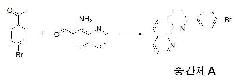
둥근 바닥 플라스크에 1-(4-브로모페닐)에타논 (1-(1-bromophenyl)ethanone) (11.5g, 0.058mol), 8-아미노퀴놀린-7-카발데히드 (8-aminoquinoline-7-carbaldehyde)(10g, 0.058mol), ABS 에탄올(Absolute EtOH) 800mL, 수산화칼륨(KOH) 13g을 넣고 온도를 승온하여 환류시키고 15시간 동안 교반한다. 반응액을 상온으로 냉각한 후 디클로로메탄(CH2Cl2, MC)/물로 추출하여 유기층을 회수한다. 유기층을 감압농축한 후 산화알루미늄(Al2O3)을 사용하여 디클로로메탄을 전개시켜 컬럼분리하여 9.5g의 중간체 A를 수득하였다. In a round bottom flask, 1-(4-bromophenyl)ethanone (11.5 g, 0.058 mol), 8-aminoquinoline-7-carbaldehyde ) (10 g, 0.058 mol), 800 mL of ABS ethanol (Absolute EtOH), and 13 g of potassium hydroxide (KOH) were added, the temperature was raised to reflux, and the mixture was stirred for 15 hours. After cooling the reaction solution to room temperature, the organic layer was recovered by extracting with dichloromethane (CH 2 Cl 2 , MC)/water. After concentrating the organic layer under reduced pressure, dichloromethane was developed using aluminum oxide (Al 2 O 3 ) to obtain 9.5 g of Intermediate A through column separation.
2) 화합물 PN03_A02 (2-(4-(10-phenylanthracen-9-yl)phenyl)-1,10-phenanthroline)의 합성2) Synthesis of compound PN03_A02 (2-(4-(10-phenylanthracen-9-yl)phenyl)-1,10-phenanthroline)

둥근 바닥 플라스크에 중간체 A 2.68g (8mmol), 9-페닐안트라센-10-보로닉산 (9-phenylanthracene-10-boronic acid) (2.8g, 9mmol), 테트라키스(트리페닐포스핀)팔라듐(0) (0.4g, 0.3mmol), 톨루엔 60mL, 에탄올 15mL, 2M 탄산칼륨 8ml을 넣고 12시간 동안 환류 교반시켰다. 반응 종료 후 반응액을 여과하여 크루드(Crude)상태의 생성물을 얻는다. 여과된 크루드 상태의 생성물을 클로로포름(CHCl3)에 가열하여 녹인 후, 산화알루미늄(Al2O3)에 감압여과한 후 농축하여 재결정하여 1.8g의 PN03_A02 화합물을 수득하였다.In a round bottom flask, intermediate A 2.68g (8mmol), 9-phenylanthracene-10-boronic acid (2.8g, 9mmol), tetrakis(triphenylphosphine)palladium(0) (0.4g, 0.3mmol), toluene 60mL, ethanol 15mL, and 2M potassium carbonate 8ml were added and refluxed and stirred for 12 hours. After completion of the reaction, the reaction solution is filtered to obtain a crude product. The filtered crude product was dissolved by heating in chloroform (CHCl 3 ), filtered under reduced pressure in aluminum oxide (Al 2 O 3 ), concentrated and recrystallized to obtain 1.8 g of a PN03_A02 compound.
3) 화합물 화합물 PN03_A03 의 합성3) Synthesis of Compound Compound PN03_A03

둥근 바닥 플라스크에 중간체 A 2.68g (8mmol), 9-페닐안트라센-10-보로닉산(9-phenylanthracene-10-boronic acid) (2.8g, 9mmol), 테트라키스(트리페닐포스핀)팔라듐(0) (0.4g, 0.3mmol), 톨루엔 60mL, 에탄올 15 mL, 2M 탄산칼륨 8ml을 넣고 12시간 동안 환류 교반시켰다. 반응 종료 후 반응액을 여과하여 크루드(Crude)상태의 생성물을 얻는다. 여과된 크루드 상태의 생성물을 클로로포름(CHCl3)에 가열하여 녹인 후, 산화알루미늄(Al2O3)에 감압여과한 후 농축하여 재결정하여 1.8g의 PN03_A03 화합물을 수득하였다.In a round bottom flask, 2.68 g (8 mmol) of intermediate A, 9-phenylanthracene-10-boronic acid (2.8 g, 9 mmol), tetrakis (triphenylphosphine) palladium (0) (0.4g, 0.3mmol), toluene 60mL, ethanol 15mL, and 2M potassium carbonate 8ml were added and refluxed and stirred for 12 hours. After completion of the reaction, the reaction solution is filtered to obtain a crude product. The filtered crude product was dissolved by heating in chloroform (CHCl 3 ), filtered under reduced pressure in aluminum oxide (Al 2 O 3 ), concentrated and recrystallized to obtain 1.8 g of a PN03_A03 compound.
합성예synthesis example 2 : 2 : 트리아진 화합물의of triazine compounds 합성 synthesis
1) 화합물 TA03_A05의 합성1) Synthesis of Compound TA03_A05


질소 분위기하에서 2-(4,4,5,5-테트라메틸-1,3,2-다이옥시보로렌-2-일)-4,6-다이페닐-1,3,5-트리아진 (2-(4,4,5,5-tetramethyl-1,3,2-dioxaborolan-2-yl)-4,6-diphenyl-1,3,5-triazine) (5.00g 13.9mmol), 중간체 C (5.63g 11.6mmol), 테트라키스트리페닐포스핀 팔라듐(0) (tetrakistriphenylphosphine palladium (0)) (Pd(PPh3)4) (0.53g 0.46mmol), 4M 포타슘 카보네이트 (potassium carbonate) 수용액 (10ml), 톨루엔 (tolulene) 30ml, 에탄올 (ethanol) 10ml을 넣고 12시간 환류 교반시켰다. 반응이 끝난 후 H2O 50ml을 넣고 3시간 교반 후 감압 여과하고 메틸렌 클로라이드 (methylene chloride)와 헥산 (hexane)을 용리제 (eluent)로 사용하여 컬럼크로마토그래피 (column chromatography)로 분리 후 MC 재결정하여 5.6g의 화합물 TA03_A05를 얻었다.2-(4,4,5,5-tetramethyl-1,3,2-dioxyborolen-2-yl)-4,6-diphenyl-1,3,5-triazine (2- (4,4,5,5-tetramethyl-1,3,2-dioxaborolan-2-yl)-4,6-diphenyl-1,3,5-triazine) (5.00 g 13.9 mmol), intermediate C (5.63 g 11.6mmol), tetrakistriphenylphosphine palladium (0) (Pd(PPh 3 ) 4 ) (0.53g 0.46mmol), 4M potassium carbonate aqueous solution (10ml), toluene ( Tolulene) 30ml, ethanol (ethanol) 10ml was added and stirred under reflux for 12 hours. After the reaction was completed, 50 ml of H 2 O was added, stirred for 3 hours, filtered under reduced pressure, separated by column chromatography using methylene chloride and hexane as eluents, and then MC recrystallized. 5.6 g of compound TA03_A05 was obtained.
2) 화합물 TA03_A04의 합성2) Synthesis of Compound TA03_A04


질소 분위기하에서 2-(4,4,5,5-테트라메틸-1,3,2-다이옥시보로렌-2-일)-4,6-다이페닐-1,3,5-트리아진 (2-(4,4,5,5-tetramethyl-1,3,2-dioxaborolan-2-yl)-4,6-diphenyl-1,3,5-triazine) (5.00g 13.9mmol), 중간체 C (5.70g 11.6mmol), 테트라키스트리페닐포스핀 팔라듐(0) (tetrakistriphenylphosphine palladium (0)) (Pd(PPh3)4) (0.53g 0.46mmol), 4M 포타슘 카보네이트 (potassium carbonate) 수용액 (10ml), 톨루엔 (tolulene) 30ml, 에탄올 (ethanol) 10ml을 넣고 12시간 환류 교반시켰다. 반응이 끝난 후 H2O 50ml을 넣고 3시간 교반 후 감압 여과하고 메틸렌 클로라이드 (methylene chloride) 와 헥산 (hexane)을 용리제 (eluent)로 사용하여 컬럼크로마토그래피 (column chromatography)로 분리 후 MC 재결정하여 5.2g의 화합물 TA03_A04를 얻었다.2-(4,4,5,5-tetramethyl-1,3,2-dioxyborolen-2-yl)-4,6-diphenyl-1,3,5-triazine (2- (4,4,5,5-tetramethyl-1,3,2-dioxaborolan-2-yl)-4,6-diphenyl-1,3,5-triazine) (5.00 g 13.9 mmol), Intermediate C (5.70 g 11.6mmol), tetrakistriphenylphosphine palladium (0) (Pd(PPh 3 ) 4 ) (0.53g 0.46mmol), 4M potassium carbonate aqueous solution (10ml), toluene ( Tolulene) 30ml, ethanol (ethanol) 10ml was added and stirred under reflux for 12 hours. After the reaction was completed, 50 ml of H 2 O was added, stirred for 3 hours, filtered under reduced pressure, separated by column chromatography using methylene chloride and hexane as eluents, and then MC recrystallized. 5.2 g of compound TA03_A04 was obtained.
3) 화합물 TA03_A07의 합성3) Synthesis of Compound TA03_A07


질소 분위기하에서 2-(4,4,5,5-테트라메틸-1,3,2-다이옥시보로렌-2-일)-4,6-다이페닐-1,3,5-트리아진 (2-(4,4,5,5-tetramethyl-1,3,2-dioxaborolan-2-yl)-4,6-diphenyl-1,3,5-triazine) (5.00g 13.9mmol), 중간체 D (5.63g 11.6mmol), 테트라키스트리페닐포스핀 팔라듐(0) (tetrakistriphenylphosphine palladium (0)) (Pd(PPh3)4) (0.53g 0.46mmol), 4M 포타슘 카보네이트 (potassium carbonate) 수용액 (10ml), 톨루엔 (tolulene) 30ml, 에탄올 (ethanol) 10ml을 넣고 12시간 환류 교반시켰다. 반응이 끝난 후 H2O 50ml을 넣고 3시간 교반 후 감압 여과하고 메틸렌 클로라이드 (methylene chloride)와 헥산 (hexane)을 용리제 (eluent)로 사용하여 컬럼 크로마토그래피 (column chromatography)로 분리 후 MC 재결정하여 4.8g 화합물 TA03_A07를 얻었다.2-(4,4,5,5-tetramethyl-1,3,2-dioxyborolen-2-yl)-4,6-diphenyl-1,3,5-triazine (2- (4,4,5,5-tetramethyl-1,3,2-dioxaborolan-2-yl)-4,6-diphenyl-1,3,5-triazine) (5.00 g 13.9 mmol), intermediate D (5.63 g 11.6mmol), tetrakistriphenylphosphine palladium (0) (Pd(PPh 3 ) 4 ) (0.53g 0.46mmol), 4M potassium carbonate aqueous solution (10ml), toluene ( Tolulene) 30ml, ethanol (ethanol) 10ml was added and stirred under reflux for 12 hours. After the reaction was completed, 50 ml of H 2 O was added, stirred for 3 hours, filtered under reduced pressure, separated by column chromatography using methylene chloride and hexane as eluents, and then MC recrystallized. 4.8g compound TA03_A07 was obtained.
이하, 전술한 화합물들을 전자수송층 또는 N형 전하생성층으로 사용하여 유기발광소자를 제작한 실시예를 개시한다. 아래의 유기막들의 두께나 형성 조건 등이 본 발명의 범위를 제한하는 것은 아니다.Hereinafter, an embodiment of fabricating an organic light emitting device using the aforementioned compounds as an electron transport layer or an N-type charge generation layer will be described. The thickness or formation conditions of the organic layers below do not limit the scope of the present invention.
실험 1 : 혼합층 유무에 따른 소자의 특성 측정Experiment 1: Measurement of device characteristics according to the presence or absence of a mixed layer
비교예comparative example 1 One
ITO 기판 상에 정공주입층, 정공수송층, 청색 발광층, 전자수송층, N형 전하생성층, P형 전하생성층, 정공수송층, 노란색 발광층, 전자수송층, 전자주입층 및 음극을 형성하여 2 스택 구조의 유기발광소자를 제조하였다. 여기서, 전자수송층은 이미다졸 화합물로 형성하고 N형 전하생성층은 안트라센 화합물로 형성하였다. A hole injection layer, a hole transport layer, a blue light emitting layer, an electron transport layer, an N-type charge generation layer, a P-type charge generation layer, a hole transport layer, a yellow light emitting layer, an electron transport layer, an electron injection layer, and a cathode are formed on an ITO substrate to form a two-stack structure. An organic light emitting device was manufactured. Here, the electron transport layer was formed of an imidazole compound and the N-type charge generation layer was formed of an anthracene compound.
비교예comparative example 2 2
전술한 비교예 1과 동일한 구성으로, 전자수송층과 N형 전하생성층을 각각 이미다졸 화합물과 안트라센 화합물을 혼합하여 형성한 것만을 달리하여 소자를 제조하였다.A device was manufactured with the same configuration as in Comparative Example 1, except that the electron transport layer and the N-type charge generation layer were formed by mixing an imidazole compound and an anthracene compound, respectively.
전술한 비교예 1과 2에 따라 제조된 소자의 구동전압에 따른 전류밀도를 측정하여 도 9에 나타내었고, 휘도에 따른 발광효율을 측정하여 도 10에 나타내었으며, 휘도에 따른 양자효율을 측정하여 도 11에 나타내었고, 이 구동전압, 발광효율 및 양자효율을 하기 표 1에 나타내었다. (구동전압, 발광효율 및 양자효율은 비교예 1의 값을 100%로 보고 그에 따른 비교예 2의 값을 퍼센트로 표시하였고, 소자의 구동 전류는 10mA/㎠이다.) The current density according to the driving voltage of the device manufactured according to Comparative Examples 1 and 2 is measured and shown in FIG. 9, and the luminous efficiency according to the luminance is measured and shown in FIG. 11, and the driving voltage, luminous efficiency and quantum efficiency are shown in Table 1 below. (For the driving voltage, luminous efficiency and quantum efficiency, the value of Comparative Example 1 was regarded as 100%, and the value of Comparative Example 2 was expressed as a percentage, and the driving current of the device was 10 mA/cm 2 .)
도 9 내지 도 11, 상기 표 1을 참조하면, 전자수송층과 N형 전하생성층을 재료의 혼합으로 구성하지 않은 비교예 1에 비해, 전자수송층과 N형 전하생성층을 재료의 혼합으로 구성한 비교예 2는 구동전압이 1% 감소되고 발광효율과 양자효율이 1% 증가되었다.9 to 11 and Table 1, compared to Comparative Example 1 in which the electron transport layer and the N-type charge generation layer were not composed of a mixture of materials, the electron transport layer and the N-type charge generation layer were composed of a mixture of materials. In Example 2, the driving voltage was reduced by 1% and the luminous efficiency and quantum efficiency were increased by 1%.
이 결과를 통해, 전자수송층과 N형 전하생성층을 이미다졸 화합물과 안트라센 화합물로 혼합하여 구성하더라도 소자의 특성 변화가 미비하다는 것을 확인하였다.Through this result, it was confirmed that even if the electron transport layer and the N-type charge generation layer were mixed with an imidazole compound and an anthracene compound, the change in the characteristics of the device was insignificant.
실험 2 : 혼합층으로 구성된 전자수송층을 구비한 소자의 특성 측정Experiment 2: Measurement of characteristics of a device having an electron transport layer composed of a mixed layer
실시예Example 1 One
전술한 비교예 1과 동일한 구성으로, 전자수송층을 트리아진 화합물 TA03_A04와 페난쓰롤린 화합물 PN03_A02를 혼합하여 형성하고 N형 전하생성층을 페난쓰롤린 화합물 PN03_A02로 형성한 것만을 달리하여 소자를 제조하였다.In the same configuration as in Comparative Example 1, the electron transport layer was formed by mixing the triazine compound TA03_A04 and the phenanthroline compound PN03_A02, and the N-type charge generation layer was formed with the phenanthroline compound PN03_A02. A device was manufactured. .
실시예Example 2 2
전술한 비교예 1과 동일한 구성으로, 전자수송층을 트리아진 화합물 TA03_A04와 페난쓰롤린 화합물 PN03_A03을 혼합하여 형성하고 N형 전하생성층을 페난쓰롤린 화합물 PN03_A03으로 형성한 것만을 달리하여 소자를 제조하였다.In the same configuration as in Comparative Example 1 described above, the electron transport layer was formed by mixing the triazine compound TA03_A04 and the phenanthroline compound PN03_A03, and the N-type charge generation layer was formed with the phenanthroline compound PN03_A03. A device was manufactured. .
전술한 비교예 1과 실시예 1에 따라 제조된 소자의 구동전압에 따른 전류밀도를 측정하여 도 12에 나타내었고, 휘도에 따른 양자효율을 측정하여 도 13에 나타내었다. 또한, 비교예 1과 실시예 2에 따라 제조된 소자의 구동전압에 따른 전류밀도를 측정하여 도 14에 나타내었고, 휘도에 따른 양자효율을 측정하여 도 15에 나타내었다. 이들의 구동전압 및 양자효율을 하기 표 2에 나타내었다. (구동전압 및 양자효율은 비교예 1의 값을 100%로 보고 그에 따른 실시예 1과 2의 값을 퍼센트로 표시하였고, 소자의 구동 전류는 10mA/㎠이다.) The current density according to the driving voltage of the devices manufactured according to Comparative Example 1 and Example 1 was measured and shown in FIG. 12, and the quantum efficiency according to luminance was measured and shown in FIG. In addition, the current density according to the driving voltage of the devices manufactured according to Comparative Example 1 and Example 2 was measured and shown in FIG. 14, and the quantum efficiency according to luminance was measured and shown in FIG. 15. Their driving voltages and quantum efficiencies are shown in Table 2 below. (For driving voltage and quantum efficiency, the value of Comparative Example 1 was regarded as 100%, and the values of Examples 1 and 2 were expressed as percentages, and the driving current of the device was 10 mA/cm 2 .)
상기 도 12 내지 도 15 및 표 2를 참조하면, 전자수송층과 N형 전하생성층을 재료의 혼합으로 구성하지 않은 비교예 1에 비해, 전자수송층을 트리아진 화합물과 페난쓰롤린 화합물의 혼합으로 구성하고 N형 전하생성층을 페난쓰롤린 화합물로 구성한 실시예 1은 구동전압이 6.07% 감소되고 양자효율이 1.42% 증가되었고 실시예 2는 구동전압이 6.25% 감소되고 양자효율이 1.42% 증가되었다.Referring to FIGS. 12 to 15 and Table 2, compared to Comparative Example 1 in which the electron transport layer and the N-type charge generation layer were not composed of a mixture of materials, the electron transport layer was composed of a mixture of a triazine compound and a phenanthroline compound. In Example 1, in which the N-type charge generation layer was composed of a phenanthroline compound, the driving voltage was reduced by 6.07% and the quantum efficiency was increased by 1.42%, and in Example 2, the driving voltage was reduced by 6.25% and the quantum efficiency was increased by 1.42%.
이 결과를 통해, 트리아진 화합물과 페난쓰롤린 화합물의 혼합으로 구성된 전자수송층을 구비함으로써, 소자의 구동전압이 감소되고 양자효율이 증가됨을 확인하였다. Through this result, it was confirmed that the driving voltage of the device was reduced and the quantum efficiency was increased by providing an electron transport layer composed of a mixture of a triazine compound and a phenanthroline compound.
실험 3 : 혼합층으로 구성된 N형 전하생성층을 구비한 소자의 특성 측정Experiment 3: Measurement of characteristics of a device having an N-type charge generation layer composed of a mixed layer
실시예Example 3 3
전술한 비교예 1과 동일한 구성으로, 전자수송층을 트리아진 화합물 TA03_A07로 형성하고, N형 전하생성층을 트리아진 화합물 TA03_A07과 페난쓰롤린 화합물 PN03_A22를 혼합하여 형성한 것만을 달리하여 소자를 제조하였다.With the same configuration as in Comparative Example 1 described above, the electron transport layer was formed with the triazine compound TA03_A07, and the N-type charge generation layer was formed by mixing the triazine compound TA03_A07 and the phenanthroline compound PN03_A22. A device was manufactured. .
실시예Example 4 4
전술한 비교예 1과 동일한 구성으로, 전자수송층을 트리아진 화합물 TA02_A24로 형성하고, N형 전하생성층을 트리아진 화합물 TA02_A24과 페난쓰롤린 화합물 PN03_A16을 혼합하여 형성한 것만을 달리하여 소자를 제조하였다.In the same configuration as in Comparative Example 1 described above, the electron transport layer was formed with the triazine compound TA02_A24, and the N-type charge generation layer was formed by mixing the triazine compound TA02_A24 and the phenanthroline compound PN03_A16. A device was manufactured. .
전술한 비교예 1과 실시예 3에 따라 제조된 소자의 구동전압에 따른 전류밀도를 측정하여 도 16에 나타내었고, 휘도에 따른 양자효율을 측정하여 도 17에 나타내었다. 또한, 비교예 1과 실시예 4에 따라 제조된 소자의 구동전압에 따른 전류밀도를 측정하여 도 18에 나타내었고, 휘도에 따른 양자효율을 측정하여 도 19에 나타내었다. 이들의 구동전압 및 양자효율을 하기 표 3에 나타내었다. (구동전압 및 양자효율은 비교예 1의 값을 100%로 보고 그에 따른 실시예 3과 4의 값을 퍼센트로 표시하였고, 소자의 구동 전류는 10mA/㎠이다.) The current density according to the driving voltage of the devices manufactured according to Comparative Example 1 and Example 3 was measured and shown in FIG. 16, and the quantum efficiency according to luminance was measured and shown in FIG. In addition, the current density according to the driving voltage of the devices manufactured according to Comparative Example 1 and Example 4 was measured and shown in FIG. 18, and the quantum efficiency according to luminance was measured and shown in FIG. Their driving voltages and quantum efficiencies are shown in Table 3 below. (For driving voltage and quantum efficiency, the value of Comparative Example 1 was regarded as 100%, and the values of Examples 3 and 4 were expressed as percentages, and the driving current of the device was 10 mA/cm 2 .)
상기 도 16 내지 도 19 및 표 3을 참조하면, 전자수송층과 N형 전하생성층을 재료의 혼합으로 구성하지 않은 비교예 1에 비해, 전자수송층을 트리아진 화합물로 구성하고, N형 전하생성층을 트리아진 화합물과 페난쓰롤린 화합물로 구성한 실시예 3은 구동전압이 2.95% 감소되고 양자효율이 2.34% 증가되었고 실시예 4는 구동전압이 2.86% 감소되고 양자효율이 2.35% 증가되었다.16 to 19 and Table 3, compared to Comparative Example 1 in which the electron transport layer and the N-type charge generation layer were not composed of a mixture of materials, the electron transport layer was composed of a triazine compound and the N-type charge generation layer In Example 3 composed of a triazine compound and a phenanthroline compound, the driving voltage was reduced by 2.95% and the quantum efficiency was increased by 2.34%, and in Example 4, the driving voltage was reduced by 2.86% and the quantum efficiency was increased by 2.35%.
이 결과를 통해, 트리아진 화합물과 페난쓰롤린 화합물의 혼합으로 구성된 전자수송층을 구비함으로써, 소자의 구동전압이 감소되고 양자효율이 증가됨을 확인하였다. Through this result, it was confirmed that the driving voltage of the device was reduced and the quantum efficiency was increased by providing an electron transport layer composed of a mixture of a triazine compound and a phenanthroline compound.
실험 4 : 혼합층으로 구성된 전자수송층과 N형 전하생성층을 구비한 소자의 특성 측정Experiment 4: Measurement of characteristics of a device having an electron transport layer composed of a mixed layer and an N-type charge generation layer
실시예Example 5 5
전술한 비교예 1과 동일한 구성으로, 전자수송층을 트리아진 화합물 TA03_A05와 TA02-A24를 1:1로 혼합하여 형성하고, N형 전하생성층을 트리아진 화합물 TA03_A05와 페난쓰롤린 화합물 PN03_A16을 혼합하여 형성한 것만을 달리하여 소자를 제조하였다. In the same configuration as in Comparative Example 1, the electron transport layer was formed by mixing the triazine compound TA03_A05 and TA02-A24 in a 1: 1 ratio, and the N-type charge generation layer was formed by mixing the triazine compound TA03_A05 and the phenanthroline compound PN03_A16. A device was manufactured by changing only the formation.
실시예Example 6 6
전술한 실시예 5와 동일한 구성으로, 전자수송층을 트리아진 화합물 TA03_A05와 TA02-A24를 2:1로 혼합하여 형성한 것만을 달리하여 소자를 제조하였다.With the same configuration as in Example 5 described above, a device was manufactured except that the electron transport layer was formed by mixing the triazine compounds TA03_A05 and TA02-A24 in a ratio of 2:1.
실시예Example 7 7
전술한 실시예 5와 동일한 구성으로, 전자수송층을 트리아진 화합물 TA03_A05와 TA19-A23을 혼합하여 형성하고, N형 전하생성층을 페난쓰롤린 화합물 PN03_A02와 PN03_A16을 혼합하여 형성한 것만을 달리하여 소자를 제조하였다.In the same configuration as in Example 5, the electron transport layer was formed by mixing the triazine compounds TA03_A05 and TA19-A23, and the N-type charge generation layer was formed by mixing the phenanthroline compounds PN03_A02 and PN03_A16. Device was manufactured.
전술한 비교예 1, 실시예 5 및 실시예 6에 따라 제조된 소자의 구동전압에 따른 전류밀도를 측정하여 도 20에 나타내었고, 휘도에 따른 양자효율을 측정하여 도 21에 나타내었다. 또한, 비교예 1과 실시예 7에 따라 제조된 소자의 구동전압에 따른 전류밀도를 측정하여 도 22에 나타내었고, 휘도에 따른 양자효율을 측정하여 도 23에 나타내었다. 이들의 구동전압 및 양자효율을 하기 표 4에 나타내었다. (구동전압 및 양자효율은 비교예 1의 값을 100%로 보고 그에 따른 실시예 5, 6 및 7의 값을 퍼센트로 표시하였고, 소자의 구동 전류는 10mA/㎠이다.) The current density according to the driving voltage of the devices manufactured according to Comparative Example 1, Example 5, and Example 6 was measured and shown in FIG. 20, and the quantum efficiency according to luminance was measured and shown in FIG. In addition, the current density according to the driving voltage of the devices manufactured according to Comparative Example 1 and Example 7 was measured and shown in FIG. 22, and the quantum efficiency according to luminance was measured and shown in FIG. Their driving voltages and quantum efficiencies are shown in Table 4 below. (For driving voltage and quantum efficiency, the value of Comparative Example 1 was regarded as 100%, and the values of Examples 5, 6, and 7 were expressed in percent, and the driving current of the device was 10 mA/cm 2 .)
상기 도 20, 도 21 및 표 4를 참조하면, 전자수송층과 N형 전하생성층을 재료의 혼합으로 구성하지 않은 비교예 1에 비해, 전자수송층을 트리아진 화합물들로 구성하고 N형 전하생성층을 페난쓰롤린 화합물과 트리아진 화합물로 구성한 실시예 5는 구동전압이 3.03% 감소되고 양자효율이 3.83% 증가되었고 실시예 6은 구동전압이 5.15% 감소되고 양자효율이 5.31% 증가되었다. 특히, TA03_A05와 TA02-A24를 1:1로 혼합하여 전자수송층을 구성한 실시예 5에 비해, TA03_A05와 TA02-A24를 2:1로 혼합하여 전자수송층을 구성한 실시예 6의 소자 구동전압이 더 감소되고 양자효율이 더 증가된 것을 확인하였다. 20, 21 and Table 4, compared to Comparative Example 1 in which the electron transport layer and the N-type charge generation layer were not composed of a mixture of materials, the electron transport layer was composed of triazine compounds and the N-type charge generation layer In Example 5 composed of a phenanthroline compound and a triazine compound, the driving voltage was reduced by 3.03% and the quantum efficiency was increased by 3.83%, and in Example 6, the driving voltage was reduced by 5.15% and the quantum efficiency was increased by 5.31%. In particular, compared to Example 5 in which the electron transport layer was formed by mixing TA03_A05 and TA02-A24 in a ratio of 1:1, the device driving voltage in Example 6 in which the electron transport layer was formed by mixing TA03_A05 and TA02-A24 in a ratio of 2:1 was further reduced. It was confirmed that the quantum efficiency was further increased.
이 결과를 통해, 트리아진 화합물들이 혼합된 전자수송층에서 특정 재료의 혼합비를 조절하여 소자의 구동전압과 양자효율 특성을 향상시킬 수 있음을 확인하였다.Through this result, it was confirmed that the driving voltage and quantum efficiency characteristics of the device can be improved by adjusting the mixing ratio of a specific material in the electron transport layer in which the triazine compounds are mixed.
또한, 상기 도 22, 도 23 및 표 4를 참조하면, 전자수송층과 N형 전하생성층을 재료의 혼합으로 구성하지 않은 비교예 1에 비해, 전자수송층을 트리아진 화합물들로 구성하고 N형 전하생성층을 페난쓰롤린 화합물들로 구성한 실시예 7은 구동전압이 동등 수준을 나타내나 양자효율이 23.20% 증가되었다. In addition, referring to FIGS. 22, 23 and Table 4, compared to Comparative Example 1 in which the electron transport layer and the N-type charge generation layer were not composed of a mixture of materials, the electron transport layer was composed of triazine compounds and N-type charge generation layer was formed. In Example 7, in which the generated layer was composed of phenanthroline compounds, the driving voltage was the same, but the quantum efficiency was increased by 23.20%.
이 결과를 통해, 트리아진 화합물들의 혼합으로 구성된 전자수송층과 페난쓰롤린 화합물들의 혼합으로 구성된 N형 전하생성층을 구비함으로써, 소자의 구동전압을 동등 수준으로 유지하면서 양자효율을 현저히 증가시킬 수 있음을 확인하였다. Through this result, by providing an electron transport layer composed of a mixture of triazine compounds and an N-type charge generation layer composed of a mixture of phenanthroline compounds, the quantum efficiency can be significantly increased while maintaining the driving voltage of the device at the same level. confirmed.
100 : 유기발광소자 110 : 양극
120 : 제1 정공주입층 130 : 제1 정공수송층
140 : 제1 발광층 150 : 제1 전자수송층
160N : N형 전하생성층 160P : P형 전하생성층
170 : 제2 정공주입층 180 : 제2 정공수송층
190 : 제2 발광층 200 : 제2 전자수송층
210 : 전자주입층 220 : 음극100: organic light emitting element 110: anode
120: first hole injection layer 130: first hole transport layer
140: first light emitting layer 150: first electron transport layer
160N: N-type
170: second hole injection layer 180: second hole transport layer
190: second light emitting layer 200: second electron transport layer
210: electron injection layer 220: cathode
Claims (13)
상기 발광부들 사이에 위치하는 P형 전하생성층; 및
상기 발광층과 상기 P형 전하생성층 사이에 위치하는 적어도 하나의 혼합층을 포함하며,
상기 혼합층은 하기 화학식 1로 표시되는 트리아진 화합물들의 혼합층, 하기 화학식 2로 표시되는 페난쓰롤린 화합물들의 혼합층 또는 이들의 혼합층으로 이루어지고,
상기 혼합층은 제1 혼합층 및 상기 제1 혼합층 상에 위치하는 제2 혼합층을 포함하며, 상기 제1 혼합층은 전자수송층이고 상기 제2 혼합층은 N형 전하생성층이고, 상기 제1 혼합층은 상기 트리아진 화합물들의 혼합 또는 상기 트리아진 화합물과 상기 페난쓰롤린 화합물의 혼합으로 이루어지며 상기 제2 혼합층은 상기 페난쓰롤린 화합물들의 혼합 또는 상기 트리아진 화합물과 상기 페난쓰롤린 화합물의 혼합으로 이루어지는 것을 특징으로 하는 유기발광소자.
[화학식 1]

상기 화학식 1에서, X1 내지 X10은 각각 독립적으로 CH 또는 C(R1) 또는 C(R2)이며, R1 과 R2는 각각 독립적으로 탄소수 6 내지 50의 방향족 고리화합물 중에서 선택되거나 N, S, O 또는 Si 원자가 1개 이상 포함되고 탄소수 5 내지 50의 이형 고리화합물 중에서 선택되고, 상기 C(R1)이나 C(R2)는 각각 같은 고리 내에 존재하거나 존재하지 않는다.
[화학식 2]

상기 화학식 2에서, X1 내지 X6은 각각 독립적으로 CH 또는 C(R1) 또는 C(R2)이며, R1 과 R2는 각각 독립적으로 탄소수 6 내지 50의 방향족 고리화합물 중에서 선택되거나 N, S, O 또는 Si 원자가 1개 이상 포함되고 탄소수 5 내지 50의 이형 고리화합물 중에서 선택되고, 상기 C(R1)이나 C(R2)는 각각 같은 고리 내에 존재하거나 존재하지 않는다. Light emitting units located between the anode and the cathode, each including a light emitting layer;
a P-type charge generation layer positioned between the light emitting units; and
At least one mixed layer positioned between the light emitting layer and the P-type charge generation layer,
The mixed layer is composed of a mixed layer of triazine compounds represented by Formula 1 below, a mixed layer of phenanthroline compounds represented by Formula 2 below, or a mixed layer thereof,
The mixed layer includes a first mixed layer and a second mixed layer disposed on the first mixed layer, the first mixed layer is an electron transport layer, the second mixed layer is an N-type charge generation layer, and the first mixed layer is the triazine. A mixture of compounds or a mixture of the triazine compound and the phenanthroline compound, and the second mixed layer is a mixture of the phenanthroline compounds or a mixture of the triazine compound and the phenanthroline compound. Characterized in that organic light-emitting device.
[Formula 1]
In Formula 1, X 1 to X 10 are each independently CH or C(R 1 ) or C(R 2 ), and R 1 and R 2 are each independently selected from aromatic ring compounds having 6 to 50 carbon atoms or N , It is selected from heterocyclic compounds containing one or more S, O or Si atoms and having 5 to 50 carbon atoms, and the C(R 1 ) or C(R 2 ) is present or absent in the same ring, respectively.
[Formula 2]
In Formula 2, X 1 to X 6 are each independently CH or C(R 1 ) or C(R 2 ), and R 1 and R 2 are each independently selected from aromatic ring compounds having 6 to 50 carbon atoms or N , It is selected from heterocyclic compounds containing one or more S, O or Si atoms and having 5 to 50 carbon atoms, and the C(R 1 ) or C(R 2 ) is present or absent in the same ring, respectively.
상기 화학식 1로 표시되는 트리아진 화합물은 하기 표시되는 화합물들 중에서 선택된 어느 하나인 것을 특징으로 하는 유기발광소자.


An organic light emitting device, characterized in that the triazine compound represented by Formula 1 is any one selected from compounds represented by the following.
상기 R1 및 R2는 각각 독립적으로 하기 표시되는 화합물들 중에서 선택된 어느 하나인 것을 특징으로 하는 유기발광소자.


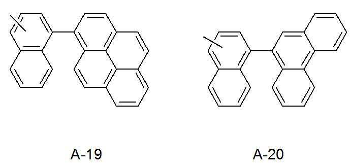


상기 화합물들에 있어서,


The R 1 and R 2 are each independently an organic light emitting device, characterized in that any one selected from the compounds shown below.
In the above compounds,
상기 화학식 2로 표시되는 페난쓰롤린 화합물은 하기 표시되는 화합물들 중에서 선택된 어느 하나인 것을 특징으로 하는 유기발광소자.


An organic light emitting device, characterized in that the phenanthroline compound represented by Chemical Formula 2 is any one selected from the compounds represented below.
상기 발광부들 사이에 위치하는 P형 전하생성층;
상기 발광층과 상기 P형 전하생성층 사이에 위치하는 전자수송층;
상기 P형 전하생성층과 상기 전자수송층 사이에 위치하는 N형 전하생성층; 및
상기 전자수송층과 상기 N형 전하생성층 사이에 위치하는 혼합층을 포함하며,
상기 혼합층은 하기 화학식 1로 표시되는 트리아진 화합물들의 혼합층, 하기 화학식 2로 표시되는 페난쓰롤린 화합물들의 혼합층 또는 이들의 혼합층으로 이루어지고,
상기 혼합층은 제1 혼합층 및 상기 제1 혼합층 상에 위치하는 제2 혼합층을 포함하고, 상기 제1 혼합층은 상기 트리아진 화합물들의 혼합 또는 상기 트리아진 화합물과 상기 페난쓰롤린 화합물의 혼합으로 이루어지며 상기 제2 혼합층은 상기 페난쓰롤린 화합물들의 혼합 또는 상기 트리아진 화합물과 상기 페난쓰롤린 화합물의 혼합으로 이루어진 것을 특징으로 하는 유기발광소자.
[화학식 1]

상기 화학식 1에서, X1 내지 X10은 각각 독립적으로 CH 또는 C(R1) 또는 C(R2)이며, R1 과 R2는 각각 독립적으로 탄소수 6 내지 50의 방향족 고리화합물 중에서 선택되거나 N, S, O 또는 Si 원자가 1개 이상 포함되고 탄소수 5 내지 50의 이형 고리화합물 중에서 선택되고, 상기 C(R1)이나 C(R2)는 각각 같은 고리 내에 존재하거나 존재하지 않는다.
[화학식 2]

상기 화학식 2에서, X1 내지 X6은 각각 독립적으로 CH 또는 C(R1) 또는 C(R2)이며, R1 과 R2는 각각 독립적으로 탄소수 6 내지 50의 방향족 고리화합물 중에서 선택되거나 N, S, O 또는 Si 원자가 1개 이상 포함되고 탄소수 5 내지 50의 이형 고리화합물 중에서 선택되고, 상기 C(R1)이나 C(R2)는 각각 같은 고리 내에 존재하거나 존재하지 않는다.Light emitting units located between the anode and the cathode, each including a light emitting layer;
a P-type charge generation layer positioned between the light emitting units;
an electron transport layer positioned between the light emitting layer and the P-type charge generation layer;
an N-type charge generation layer positioned between the P-type charge generation layer and the electron transport layer; and
A mixed layer positioned between the electron transport layer and the N-type charge generation layer,
The mixed layer is composed of a mixed layer of triazine compounds represented by Formula 1 below, a mixed layer of phenanthroline compounds represented by Formula 2 below, or a mixed layer thereof,
The mixed layer includes a first mixed layer and a second mixed layer disposed on the first mixed layer, and the first mixed layer is made of a mixture of the triazine compounds or a mixture of the triazine compound and the phenanthroline compound. The organic light emitting device, characterized in that the second mixed layer is made of a mixture of the phenanthroline compounds or a mixture of the triazine compound and the phenanthroline compound.
[Formula 1]
In Formula 1, X 1 to X 10 are each independently CH or C(R 1 ) or C(R 2 ), and R 1 and R 2 are each independently selected from aromatic ring compounds having 6 to 50 carbon atoms or N , It is selected from heterocyclic compounds containing one or more S, O or Si atoms and having 5 to 50 carbon atoms, and the C(R 1 ) or C(R 2 ) is present or absent in the same ring, respectively.
[Formula 2]
In Formula 2, X 1 to X 6 are each independently CH or C(R 1 ) or C(R 2 ), and R 1 and R 2 are each independently selected from aromatic ring compounds having 6 to 50 carbon atoms or N , It is selected from heterocyclic compounds containing one or more S, O or Si atoms and having 5 to 50 carbon atoms, and the C(R 1 ) or C(R 2 ) is present or absent in the same ring, respectively.
Priority Applications (1)
| Application Number | Priority Date | Filing Date | Title |
|---|---|---|---|
| KR1020150086918A KR102517937B1 (en) | 2015-06-18 | 2015-06-18 | Organic light emitting device |
Applications Claiming Priority (1)
| Application Number | Priority Date | Filing Date | Title |
|---|---|---|---|
| KR1020150086918A KR102517937B1 (en) | 2015-06-18 | 2015-06-18 | Organic light emitting device |
Publications (2)
| Publication Number | Publication Date |
|---|---|
| KR20160150185A KR20160150185A (en) | 2016-12-29 |
| KR102517937B1 true KR102517937B1 (en) | 2023-04-04 |
Family
ID=57736558
Family Applications (1)
| Application Number | Title | Priority Date | Filing Date |
|---|---|---|---|
| KR1020150086918A Active KR102517937B1 (en) | 2015-06-18 | 2015-06-18 | Organic light emitting device |
Country Status (1)
| Country | Link |
|---|---|
| KR (1) | KR102517937B1 (en) |
Families Citing this family (8)
| Publication number | Priority date | Publication date | Assignee | Title |
|---|---|---|---|---|
| KR102101473B1 (en) | 2017-07-10 | 2020-04-16 | 주식회사 엘지화학 | Hetero-cyclic compound and organic light emitting device comprising the same |
| EP3480192B1 (en) * | 2017-11-06 | 2020-12-23 | Novaled GmbH | Triazine compound and organic semiconducting layer comprising the same |
| WO2019093547A1 (en) * | 2017-11-10 | 2019-05-16 | 주식회사 진웅산업 | Phenanthroline-anthracene compound and organic light emitting device comprising same |
| KR102238901B1 (en) | 2018-07-19 | 2021-04-12 | 주식회사 엘지화학 | Organic light emitting device |
| KR102509034B1 (en) | 2020-02-13 | 2023-03-10 | 삼성디스플레이 주식회사 | Organic light emitting device and apparatus including the same |
| KR102761518B1 (en) * | 2020-03-19 | 2025-02-04 | 삼성디스플레이 주식회사 | Organic light emitting device |
| CN115802861A (en) * | 2022-12-07 | 2023-03-14 | 安徽省华显新材料科技有限公司 | Organic electroluminescent device and display or lighting device including same |
| KR102608380B1 (en) * | 2023-01-09 | 2023-12-01 | 덕산네오룩스 주식회사 | An organic electronic element comprising compound for organic electronic element and an electronic device thereof |
Citations (1)
| Publication number | Priority date | Publication date | Assignee | Title |
|---|---|---|---|---|
| WO2013145666A1 (en) * | 2012-03-29 | 2013-10-03 | ソニー株式会社 | Organic electroluminescent element |
Family Cites Families (4)
| Publication number | Priority date | Publication date | Assignee | Title |
|---|---|---|---|---|
| KR101367514B1 (en) * | 2008-07-11 | 2014-02-27 | 주식회사 엘지화학 | New anthracene derivatives and organic electronic device using the same |
| JP5973661B2 (en) * | 2012-05-31 | 2016-08-23 | エルジー ディスプレイ カンパニー リミテッド | Organic light emitting device |
| KR102079254B1 (en) * | 2013-06-24 | 2020-02-20 | 삼성디스플레이 주식회사 | Organic light emitting diode |
| KR102268119B1 (en) * | 2013-08-30 | 2021-06-21 | 엘지디스플레이 주식회사 | Pyrene compound and organic light emitting diode device comprising the same |
-
2015
- 2015-06-18 KR KR1020150086918A patent/KR102517937B1/en active Active
Patent Citations (1)
| Publication number | Priority date | Publication date | Assignee | Title |
|---|---|---|---|---|
| WO2013145666A1 (en) * | 2012-03-29 | 2013-10-03 | ソニー株式会社 | Organic electroluminescent element |
Also Published As
| Publication number | Publication date |
|---|---|
| KR20160150185A (en) | 2016-12-29 |
Similar Documents
| Publication | Publication Date | Title |
|---|---|---|
| KR102815660B1 (en) | Organic light emitting device | |
| KR102679133B1 (en) | Organic Light Emitting Diode Device | |
| KR102825250B1 (en) | Organic Light Emitting Diode Device | |
| KR102525492B1 (en) | Organic light emitting device | |
| KR102559121B1 (en) | Organic Light Emitting Diode Device | |
| KR102517937B1 (en) | Organic light emitting device | |
| KR102174066B1 (en) | Organic compounds and organic light emitting diode device comprising the same | |
| KR102491790B1 (en) | Organic Light Emitting Diode Device | |
| CN105609522A (en) | Organic light emitting display device | |
| KR102702918B1 (en) | Organic Light Emitting Diode Device | |
| KR102439571B1 (en) | organic light emitting device | |
| KR102488944B1 (en) | Pyrimidine derivative and organic light emitting device comprising the same | |
| KR102145425B1 (en) | Organic compounds and organic light emitting diode device comprising the same |
Legal Events
| Date | Code | Title | Description |
|---|---|---|---|
| PA0109 | Patent application |
St.27 status event code: A-0-1-A10-A12-nap-PA0109 |
|
| PG1501 | Laying open of application |
St.27 status event code: A-1-1-Q10-Q12-nap-PG1501 |
|
| P22-X000 | Classification modified |
St.27 status event code: A-2-2-P10-P22-nap-X000 |
|
| R17-X000 | Change to representative recorded |
St.27 status event code: A-3-3-R10-R17-oth-X000 |
|
| A201 | Request for examination | ||
| PA0201 | Request for examination |
St.27 status event code: A-1-2-D10-D11-exm-PA0201 |
|
| E902 | Notification of reason for refusal | ||
| PE0902 | Notice of grounds for rejection |
St.27 status event code: A-1-2-D10-D21-exm-PE0902 |
|
| T11-X000 | Administrative time limit extension requested |
St.27 status event code: U-3-3-T10-T11-oth-X000 |
|
| AMND | Amendment | ||
| E13-X000 | Pre-grant limitation requested |
St.27 status event code: A-2-3-E10-E13-lim-X000 |
|
| P11-X000 | Amendment of application requested |
St.27 status event code: A-2-2-P10-P11-nap-X000 |
|
| P13-X000 | Application amended |
St.27 status event code: A-2-2-P10-P13-nap-X000 |
|
| PE0601 | Decision on rejection of patent |
St.27 status event code: N-2-6-B10-B15-exm-PE0601 |
|
| AMND | Amendment | ||
| E13-X000 | Pre-grant limitation requested |
St.27 status event code: A-2-3-E10-E13-lim-X000 |
|
| P11-X000 | Amendment of application requested |
St.27 status event code: A-2-2-P10-P11-nap-X000 |
|
| P13-X000 | Application amended |
St.27 status event code: A-2-2-P10-P13-nap-X000 |
|
| PX0901 | Re-examination |
St.27 status event code: A-2-3-E10-E12-rex-PX0901 |
|
| PX0701 | Decision of registration after re-examination |
St.27 status event code: A-3-4-F10-F13-rex-PX0701 |
|
| X701 | Decision to grant (after re-examination) | ||
| P22-X000 | Classification modified |
St.27 status event code: A-2-2-P10-P22-nap-X000 |
|
| P22-X000 | Classification modified |
St.27 status event code: A-2-2-P10-P22-nap-X000 |
|
| GRNT | Written decision to grant | ||
| PR0701 | Registration of establishment |
St.27 status event code: A-2-4-F10-F11-exm-PR0701 |
|
| PR1002 | Payment of registration fee |
St.27 status event code: A-2-2-U10-U11-oth-PR1002 Fee payment year number: 1 |
|
| PG1601 | Publication of registration |
St.27 status event code: A-4-4-Q10-Q13-nap-PG1601 |
|
| P22-X000 | Classification modified |
St.27 status event code: A-4-4-P10-P22-nap-X000 |
|
| P22-X000 | Classification modified |
St.27 status event code: A-4-4-P10-P22-nap-X000 |