KR102510900B1 - Semiconductor device and method for operating semiconductor device - Google Patents
Semiconductor device and method for operating semiconductor device Download PDFInfo
- Publication number
- KR102510900B1 KR102510900B1 KR1020160014250A KR20160014250A KR102510900B1 KR 102510900 B1 KR102510900 B1 KR 102510900B1 KR 1020160014250 A KR1020160014250 A KR 1020160014250A KR 20160014250 A KR20160014250 A KR 20160014250A KR 102510900 B1 KR102510900 B1 KR 102510900B1
- Authority
- KR
- South Korea
- Prior art keywords
- latency
- counter
- transaction
- identification information
- packets
- Prior art date
- Legal status (The legal status is an assumption and is not a legal conclusion. Google has not performed a legal analysis and makes no representation as to the accuracy of the status listed.)
- Active
Links
Images




Classifications
-
- H—ELECTRICITY
- H04—ELECTRIC COMMUNICATION TECHNIQUE
- H04L—TRANSMISSION OF DIGITAL INFORMATION, e.g. TELEGRAPHIC COMMUNICATION
- H04L43/00—Arrangements for monitoring or testing data switching networks
- H04L43/08—Monitoring or testing based on specific metrics, e.g. QoS, energy consumption or environmental parameters
- H04L43/0852—Delays
-
- G—PHYSICS
- G06—COMPUTING OR CALCULATING; COUNTING
- G06F—ELECTRIC DIGITAL DATA PROCESSING
- G06F13/00—Interconnection of, or transfer of information or other signals between, memories, input/output devices or central processing units
- G06F13/38—Information transfer, e.g. on bus
- G06F13/42—Bus transfer protocol, e.g. handshake; Synchronisation
- G06F13/4282—Bus transfer protocol, e.g. handshake; Synchronisation on a serial bus, e.g. I2C bus, SPI bus
-
- G—PHYSICS
- G06—COMPUTING OR CALCULATING; COUNTING
- G06F—ELECTRIC DIGITAL DATA PROCESSING
- G06F15/00—Digital computers in general; Data processing equipment in general
- G06F15/16—Combinations of two or more digital computers each having at least an arithmetic unit, a program unit and a register, e.g. for a simultaneous processing of several programs
- G06F15/177—Initialisation or configuration control
-
- G—PHYSICS
- G06—COMPUTING OR CALCULATING; COUNTING
- G06F—ELECTRIC DIGITAL DATA PROCESSING
- G06F11/00—Error detection; Error correction; Monitoring
- G06F11/30—Monitoring
- G06F11/3051—Monitoring arrangements for monitoring the configuration of the computing system or of the computing system component, e.g. monitoring the presence of processing resources, peripherals, I/O links, software programs
-
- G—PHYSICS
- G06—COMPUTING OR CALCULATING; COUNTING
- G06F—ELECTRIC DIGITAL DATA PROCESSING
- G06F11/00—Error detection; Error correction; Monitoring
- G06F11/30—Monitoring
- G06F11/34—Recording or statistical evaluation of computer activity, e.g. of down time, of input/output operation ; Recording or statistical evaluation of user activity, e.g. usability assessment
- G06F11/3409—Recording or statistical evaluation of computer activity, e.g. of down time, of input/output operation ; Recording or statistical evaluation of user activity, e.g. usability assessment for performance assessment
- G06F11/3419—Recording or statistical evaluation of computer activity, e.g. of down time, of input/output operation ; Recording or statistical evaluation of user activity, e.g. usability assessment for performance assessment by assessing time
-
- G—PHYSICS
- G06—COMPUTING OR CALCULATING; COUNTING
- G06F—ELECTRIC DIGITAL DATA PROCESSING
- G06F11/00—Error detection; Error correction; Monitoring
- G06F11/30—Monitoring
- G06F11/34—Recording or statistical evaluation of computer activity, e.g. of down time, of input/output operation ; Recording or statistical evaluation of user activity, e.g. usability assessment
- G06F11/3466—Performance evaluation by tracing or monitoring
- G06F11/349—Performance evaluation by tracing or monitoring for interfaces, buses
-
- G—PHYSICS
- G06—COMPUTING OR CALCULATING; COUNTING
- G06F—ELECTRIC DIGITAL DATA PROCESSING
- G06F13/00—Interconnection of, or transfer of information or other signals between, memories, input/output devices or central processing units
- G06F13/14—Handling requests for interconnection or transfer
-
- G—PHYSICS
- G06—COMPUTING OR CALCULATING; COUNTING
- G06F—ELECTRIC DIGITAL DATA PROCESSING
- G06F13/00—Interconnection of, or transfer of information or other signals between, memories, input/output devices or central processing units
- G06F13/14—Handling requests for interconnection or transfer
- G06F13/36—Handling requests for interconnection or transfer for access to common bus or bus system
- G06F13/362—Handling requests for interconnection or transfer for access to common bus or bus system with centralised access control
- G06F13/364—Handling requests for interconnection or transfer for access to common bus or bus system with centralised access control using independent requests or grants, e.g. using separated request and grant lines
-
- G—PHYSICS
- G06—COMPUTING OR CALCULATING; COUNTING
- G06F—ELECTRIC DIGITAL DATA PROCESSING
- G06F15/00—Digital computers in general; Data processing equipment in general
- G06F15/76—Architectures of general purpose stored program computers
- G06F15/78—Architectures of general purpose stored program computers comprising a single central processing unit
- G06F15/7807—System on chip, i.e. computer system on a single chip; System in package, i.e. computer system on one or more chips in a single package
-
- G—PHYSICS
- G06—COMPUTING OR CALCULATING; COUNTING
- G06F—ELECTRIC DIGITAL DATA PROCESSING
- G06F3/00—Input arrangements for transferring data to be processed into a form capable of being handled by the computer; Output arrangements for transferring data from processing unit to output unit, e.g. interface arrangements
- G06F3/06—Digital input from, or digital output to, record carriers, e.g. RAID, emulated record carriers or networked record carriers
- G06F3/0601—Interfaces specially adapted for storage systems
- G06F3/0602—Interfaces specially adapted for storage systems specifically adapted to achieve a particular effect
- G06F3/061—Improving I/O performance
- G06F3/0611—Improving I/O performance in relation to response time
-
- G—PHYSICS
- G06—COMPUTING OR CALCULATING; COUNTING
- G06F—ELECTRIC DIGITAL DATA PROCESSING
- G06F3/00—Input arrangements for transferring data to be processed into a form capable of being handled by the computer; Output arrangements for transferring data from processing unit to output unit, e.g. interface arrangements
- G06F3/06—Digital input from, or digital output to, record carriers, e.g. RAID, emulated record carriers or networked record carriers
- G06F3/0601—Interfaces specially adapted for storage systems
- G06F3/0628—Interfaces specially adapted for storage systems making use of a particular technique
- G06F3/0653—Monitoring storage devices or systems
-
- G—PHYSICS
- G06—COMPUTING OR CALCULATING; COUNTING
- G06F—ELECTRIC DIGITAL DATA PROCESSING
- G06F3/00—Input arrangements for transferring data to be processed into a form capable of being handled by the computer; Output arrangements for transferring data from processing unit to output unit, e.g. interface arrangements
- G06F3/06—Digital input from, or digital output to, record carriers, e.g. RAID, emulated record carriers or networked record carriers
- G06F3/0601—Interfaces specially adapted for storage systems
- G06F3/0668—Interfaces specially adapted for storage systems adopting a particular infrastructure
- G06F3/0671—In-line storage system
- G06F3/0683—Plurality of storage devices
- G06F3/0685—Hybrid storage combining heterogeneous device types, e.g. hierarchical storage, hybrid arrays
-
- H—ELECTRICITY
- H04—ELECTRIC COMMUNICATION TECHNIQUE
- H04L—TRANSMISSION OF DIGITAL INFORMATION, e.g. TELEGRAPHIC COMMUNICATION
- H04L43/00—Arrangements for monitoring or testing data switching networks
- H04L43/02—Capturing of monitoring data
- H04L43/028—Capturing of monitoring data by filtering
-
- G—PHYSICS
- G06—COMPUTING OR CALCULATING; COUNTING
- G06F—ELECTRIC DIGITAL DATA PROCESSING
- G06F2201/00—Indexing scheme relating to error detection, to error correction, and to monitoring
- G06F2201/88—Monitoring involving counting
Landscapes
- Engineering & Computer Science (AREA)
- Theoretical Computer Science (AREA)
- General Engineering & Computer Science (AREA)
- Physics & Mathematics (AREA)
- General Physics & Mathematics (AREA)
- Computer Hardware Design (AREA)
- Human Computer Interaction (AREA)
- Quality & Reliability (AREA)
- Computing Systems (AREA)
- Microelectronics & Electronic Packaging (AREA)
- Software Systems (AREA)
- Debugging And Monitoring (AREA)
- Data Exchanges In Wide-Area Networks (AREA)
- Computer Networks & Wireless Communication (AREA)
- Signal Processing (AREA)
- Environmental & Geological Engineering (AREA)
Abstract
반도체 장치 및 반도체 장치의 동작 방법이 제공된다. 반도체 장치의 동작 방법은 마스터 디바이스(master device)와 슬레이브 디바이스(slave device) 사이에 전송되는 복수의 요청 패킷 및 복수의 응답 패킷을 모니터링하고, 상기 복수의 요청 패킷 중 미리 설정된 식별 정보에 부합하는 타겟 요청 패킷을 검출하고, 상기 타겟 요청 패킷과, 상기 복수의 응답 패킷 중 상기 식별 정보에 부합하는 타겟 응답 패킷을 포함하는 트랜잭션(transaction)의 레이턴시(latency)를 측정하기 위한 레이턴시 카운터(latency counter)의 동작을 시작하고, 상기 복수의 응답 패킷 중 상기 타겟 응답 패킷을 검출하고, 상기 레이턴시 카운터의 동작을 중지하고, 상기 레이턴시 카운터로부터 상기 트랜잭션의 레이턴시 값을 획득하는 것을 포함한다.A semiconductor device and a method of operating the semiconductor device are provided. A method of operating a semiconductor device monitors a plurality of request packets and a plurality of response packets transmitted between a master device and a slave device, and targets a target matching predetermined identification information among the plurality of request packets. A latency counter for detecting a request packet and measuring the latency of a transaction including the target request packet and a target response packet matching the identification information among the plurality of response packets and starting an operation, detecting the target response packet among the plurality of response packets, stopping the operation of the latency counter, and obtaining a latency value of the transaction from the latency counter.
Description
본 발명은 반도체 장치 및 반도체 장치의 동작 방법에 관한 것이다.The present invention relates to a semiconductor device and a method of operating the semiconductor device.
SoC(Sytem-on-Chip)은 고성능 온 칩 인터커넥트(on-chip interconnect)를 이용하여 여러 IP 블록(Intellectual Propertcy block) 사이에서의 데이터 전송을 구현한다. 온 칩 인터커넥트는, 예컨대 임의의 마스터 디바이스(master device)와 슬레이브 디바이스(slave device) 사이의 다중 트랜잭션을 전송할 수 있다. 이와 같은 마스터 디바이스와 슬레이브 디바이스 사이에 형성되는 채널은, 예컨대 디버깅, QoS 제어, 사용자에 의해 정의된 특정 이벤트 발생 추적 등을 수행하기 위해, 모니터링 장치(monitor)에 의해 모니터링될 수 있다.System-on-Chip (SoC) implements data transmission between multiple IP blocks (Intellectual Property blocks) using a high-performance on-chip interconnect. An on-chip interconnect can transfer multiple transactions between any master device and a slave device, for example. A channel formed between such a master device and a slave device may be monitored by a monitoring device in order to perform, for example, debugging, QoS control, tracking of occurrence of a specific event defined by a user, and the like.
본 발명이 해결하고자 하는 기술적 과제는 SoC의 마스터 디바이스와 슬레이브 디바이스 사이에 형성되는 채널에서 레이턴시(latency)를 효율적으로 측정하기 위한 반도체 장치의 동작 방법을 제공하는 것이다.A technical problem to be solved by the present invention is to provide a method of operating a semiconductor device for efficiently measuring latency in a channel formed between a master device and a slave device of an SoC.
본 발명이 해결하고자 하는 다른 기술적 과제는 SoC의 마스터 디바이스와 슬레이브 디바이스 사이에 형성되는 채널에서 레이턴시(latency)를 효율적으로 측정하기 위한 반도체 장치를 제공하는 것이다.Another technical problem to be solved by the present invention is to provide a semiconductor device for efficiently measuring latency in a channel formed between a master device and a slave device of an SoC.
본 발명이 해결하고자 하는 기술적 과제들은 이상에서 언급한 기술적 과제들로 제한되지 않으며, 언급되지 않은 또 다른 기술적 과제들은 아래의 기재로부터 해당 기술 분야의 통상의 기술자에게 명확하게 이해될 수 있을 것이다.The technical problems to be solved by the present invention are not limited to the technical problems mentioned above, and other technical problems not mentioned will be clearly understood by those skilled in the art from the description below.
상기 기술적 과제를 달성하기 위한 본 발명의 일 실시예에 따른 반도체 장치의 동작 방법은, 마스터 디바이스(master device)와 슬레이브 디바이스(slave device) 사이에 전송되는 복수의 요청 패킷 및 복수의 응답 패킷을 모니터링하고, 복수의 요청 패킷 중 미리 설정된 식별 정보에 부합하는 타겟 요청 패킷을 검출하고, 타겟 요청 패킷과, 복수의 응답 패킷 중 식별 정보에 부합하는 타겟 응답 패킷을 포함하는 트랜잭션(transaction)의 레이턴시(latency)를 측정하기 위한 레이턴시 카운터(latency counter)의 동작을 시작하고, 복수의 응답 패킷 중 타겟 응답 패킷을 검출하고, 레이턴시 카운터의 동작을 중지하고, 레이턴시 카운터로부터 트랜잭션의 레이턴시 값을 획득하는 것을 포함한다.In order to achieve the above technical problem, a method for operating a semiconductor device according to an embodiment of the present invention monitors a plurality of request packets and a plurality of response packets transmitted between a master device and a slave device. , detecting a target request packet matching preset identification information among a plurality of request packets, and latency of a transaction including a target request packet and a target response packet matching identification information among a plurality of response packets. ), detecting a target response packet among a plurality of response packets, stopping the operation of the latency counter, and obtaining a latency value of the transaction from the latency counter. .
본 발명의 몇몇의 실시예에서, 상기 방법은, MO 카운터(Multiple Outstanding Counter)를 이용하여, 상기 복수의 요청 패킷 중 대응하는 응답 패킷이 아직 검출되지 않은 요청 패킷의 개수를 카운트하는 것을 더 포함할 수 있다.In some embodiments of the present invention, the method may further include counting the number of request packets for which a corresponding response packet has not yet been detected among the plurality of request packets by using a multiple outstanding counter (MO counter). can
본 발명의 몇몇의 실시예에서, 상기 방법은, RO 카운터(Response Ordering Counter)를 이용하여, 상기 복수의 요청 패킷 중 대응하는 응답 패킷이 검출되었는지 여부를 결정하는 것을 더 포함할 수 있다.In some embodiments of the present invention, the method may further include determining whether a corresponding response packet among the plurality of request packets is detected by using a response ordering counter (RO).
본 발명의 몇몇의 실시예에서, 상기 레이턴시 카운터의 동작을 시작하는 것은, 상기 MO 카운터의 MO 카운트 값을 상기 RO 카운터의 초기 값으로 설정하는 것을 포함할 수 있다.In some embodiments of the present invention, starting the operation of the latency counter may include setting the MO count value of the MO counter to an initial value of the RO counter.
본 발명의 몇몇의 실시예에서, 상기 RO 카운터의 RO 카운트 값은 상기 복수의 요청 패킷 중 대응하는 응답 패킷이 검출될 때마다 감소하고, 상기 레이턴시 카운터의 동작을 중지하는 것은, 상기 RO 카운터의 RO 카운트 값이 0이 되면 상기 레이턴시 카운터의 동작을 중지하는 것을 포함할 수 있다.In some embodiments of the present invention, the RO count value of the RO counter is decreased whenever a corresponding response packet among the plurality of request packets is detected, and stopping the operation of the latency counter is When the count value becomes 0, the operation of the latency counter may be stopped.
본 발명의 몇몇의 실시예에서, 상기 미리 설정된 식별 정보는 트랜잭션 ID 정보 및 트랜잭션 속성(attribute) 정보 중 적어도 하나를 포함할 수 있다.In some embodiments of the present invention, the preset identification information may include at least one of transaction ID information and transaction attribute information.
본 발명의 몇몇의 실시예에서, 상기 트랜잭션 ID 정보는 상기 마스터 디바이스 또는 상기 슬레이브 디바이스를 식별하기 위한 고유 ID 정보를 포함할 수 있다.In some embodiments of the present invention, the transaction ID information may include unique ID information for identifying the master device or the slave device.
본 발명의 몇몇의 실시예에서, 상기 트랜잭션 속성 정보는 버스트 길이(burth length) 속성 정보 및 캐시 스누핑 타입(cache snooping type) 속성 정보 중 적어도 하나를 포함할 수 있다.In some embodiments of the present invention, the transaction attribute information may include at least one of burst length attribute information and cache snooping type attribute information.
본 발명의 몇몇의 실시예에서, 상기 마스터 디바이스는 시스템 온 칩(System-on-Chip, SoC)에 구비된 IP 블록(Intellectual Property Block)이고, 상기 마스터 디바이스와 상기 슬레이브 디바이스는 온 칩 인터커넥트(on-chip-interconnect)를 통해 상기 복수의 요청 패킷 및 복수의 응답 패킷을 주고 받을 수 있다.In some embodiments of the present invention, the master device is an IP block (Intellectual Property Block) included in a System-on-Chip (SoC), and the master device and the slave device are on-chip interconnects (on-chip interconnects). -chip-interconnect), the plurality of request packets and the plurality of response packets can be exchanged.
본 발명의 몇몇의 실시예에서, 상기 방법은, 상기 시스템 온 칩 외부로부터 사용자 또는 어플리케이션에 의해 미리 설정된 식별 정보를 수신하는 것을 더 포함할 수 있다.In some embodiments of the present invention, the method may further include receiving identification information preset by a user or an application from outside the system-on-chip.
본 발명의 몇몇의 실시예에서, 상기 방법은, 상기 식별 정보로부터 현재 트랙 ID(current-tracked ID) 정보를 설정하는 것을 더 포함하고, 상기 타겟 요청 패킷을 검출하는 것은, 상기 마스터 디바이스와 상기 슬레이브 디바이스 사이에 형성된 채널의 상태를 결정하고, 상기 채널이 아이들(idle) 상태인 경우, 상기 식별 정보에 부합하는 타겟 요청 패킷을 검출하고, 상기 채널이 비지(busy) 상태인 경우, 상기 현재 트랙 ID 정보에 부합하는 타겟 요청 패킷을 검출하는 것을 포함할 수 있다.In some embodiments of the present invention, the method further comprises setting current-tracked ID (ID) information from the identification information, and detecting the target request packet is performed by the master device and the slave Determines the state of a channel formed between devices, detects a target request packet matching the identification information when the channel is in an idle state, and detects the current track ID when the channel is in a busy state It may include detecting a target request packet matching the information.
본 발명의 몇몇의 실시예에서, 상기 방법은, 상기 채널이 아이들 상태에서 비지 상태로 변경되는 경우, 상기 현재 트랙 ID를 업데이트하는 것을 포함할 수 있다.In some embodiments of the present invention, the method may include updating the current track ID when the channel changes from an idle state to a busy state.
본 발명의 몇몇의 실시예에서, 상기 트랜잭션은 제1 트랜잭션 및 상기 제1 트랜잭션과 다른 제2 트랜잭션을 포함하고, 상기 트랜잭션의 레이턴시 값을 획득하는 것은, 상기 제1 트랜잭션의 제1 레이턴시 값 및 상기 제2 트랜잭션의 제2 레이턴시 값을 획득하는 것을 포함하고, 상기 방법은, 상기 제1 레이턴시 값 및 상기 제2 레이턴시 값으로부터 평균 레이턴시(average latency) 및 피크 레이턴시(peak latency)를 연산하는 것을 더 포함할 수 있다.In some embodiments of the present invention, the transaction includes a first transaction and a second transaction different from the first transaction, and obtaining the latency value of the transaction comprises: obtaining the first latency value of the first transaction and the second transaction; obtaining a second latency value of a second transaction, the method further comprising calculating an average latency and a peak latency from the first latency value and the second latency value; can do.
본 발명의 몇몇의 실시예에서, 상기 방법은, 상기 평균 레이턴시 및 상기 피크 레이턴시를 이용하여 상기 마스터 디바이스와 상기 슬레이브 디바이스 사이에 형성된 채널(channel)을 디버깅하는 것을 더 포함할 수 있다.In some embodiments of the present invention, the method may further include debugging a channel formed between the master device and the slave device using the average latency and the peak latency.
본 발명의 몇몇의 실시예에서, 상기 방법은, 상기 평균 레이턴시 및 상기 피크 레이턴시를 이용하여 상기 마스터 디바이스와 상기 슬레이브 디바이스 사이에 형성된 채널(channel)의 QoS(Quality of Service)를 제어하는 것을 더 포함할 수 있다.In some embodiments of the present invention, the method further includes controlling Quality of Service (QoS) of a channel formed between the master device and the slave device using the average latency and the peak latency. can do.
상기 기술적 과제를 달성하기 위한 본 발명의 다른 실시예에 따른 반도체 장치의 동작 방법은, 시스템 온 칩(System-on-Chip, SoC)에 구비된 제1 IP 블록(Intellectual Property Block)과 제2 IP 블록 사이의 복수의 트랜잭션을 모니터링하고, 시스템 온 칩 외부로부터 미리 설정된 제1 식별 정보 및 제2 식별 정보를 입력받고, 레이턴시 카운터(latency counter)를 이용하여 복수의 트랜잭션 중 제1 식별 정보에 부합하는 제1 트랜잭션의 레이턴시를 측정하고, 레이턴시 카운터를 이용하여 복수의 트랜잭션 중 제2 식별 정보에 부합하는 제2 트랜잭션의 레이턴시를 측정하고, 제1 트랜잭션 및 제2 트랜잭션의 레이턴시로부터 평균 레이턴시(average latency) 및 피크 레이턴시(peak latency)를 연산하는 것을 포함한다.In order to achieve the above technical problem, a method for operating a semiconductor device according to another embodiment of the present invention includes a first IP block (Intellectual Property Block) and a second IP included in a System-on-Chip (SoC). Monitoring a plurality of transactions between blocks, receiving preset first identification information and second identification information from the outside of the system-on-chip, and using a latency counter to match the first identification information among the plurality of transactions The latency of the first transaction is measured, the latency of the second transaction that matches the second identification information among the plurality of transactions is measured using the latency counter, and the average latency is calculated from the latencies of the first transaction and the second transaction. and calculating peak latency.
본 발명의 몇몇의 실시예에서, 상기 트랜잭션은 요청 패킷 및 상기 요청 패킷에 대응하는 응답 패킷을 포함하고, 상기 방법은, MO 카운터(Multiple Outstanding Counter)를 이용하여, 상기 제1 트랜잭션 및 상기 제2 트랜잭션에 대해 상기 응답 패킷이 아직 검출되지 않은 상기 요청 패킷의 개수를 카운트하는 것을 더 포함할 수 있다.In some embodiments of the present invention, the transaction includes a request packet and a response packet corresponding to the request packet, and the method includes the first transaction and the second transaction using a multiple outstanding counter (MO). The method may further include counting the number of request packets for which the response packet has not yet been detected for a transaction.
본 발명의 몇몇의 실시예에서, 상기 방법은, RO 카운터(Response Ordering Counter)를 이용하여, 상기 응답 패킷이 검출되었는지 여부를 결정하는 것을 더 포함할 수 있다.In some embodiments of the present invention, the method may further include determining whether the response packet is detected by using a response ordering counter (RO).
본 발명의 몇몇의 실시예에서, 상기 레이턴시 카운터의 초기 값은 상기 MO 카운터의 MO 카운트 값을 포함할 수 있다.In some embodiments of the present invention, the initial value of the latency counter may include the MO count value of the MO counter.
본 발명의 몇몇의 실시예에서, 상기 RO 카운터의 RO 카운트 값은 상기 응답 패킷이 검출될 때마다 감소하고, 상기 레이턴시 카운터는, 상기 RO 카운터의 RO 카운트 값이 0이 되면 카운트를 중지할 수 있다.In some embodiments of the present invention, the RO count value of the RO counter is decreased each time the response packet is detected, and the latency counter may stop counting when the RO count value of the RO counter becomes 0. .
본 발명의 몇몇의 실시예에서, 상기 미리 설정된 식별 정보는 트랜잭션 ID 정보 및 트랜잭션 속성(attribute) 정보 중 적어도 하나를 포함할 수 있다.In some embodiments of the present invention, the preset identification information may include at least one of transaction ID information and transaction attribute information.
본 발명의 몇몇의 실시예에서, 상기 트랜잭션 ID 정보는 상기 마스터 디바이스 또는 상기 슬레이브 디바이스를 식별하기 위한 고유 ID 정보를 포함할 수 있다.In some embodiments of the present invention, the transaction ID information may include unique ID information for identifying the master device or the slave device.
본 발명의 몇몇의 실시예에서, 상기 트랜잭션 속성 정보는 버스트 길이(burth length) 속성 정보 및 캐시 스누핑 타입(cache snooping type) 속성 정보 중 적어도 하나를 포함할 수 있다.In some embodiments of the present invention, the transaction attribute information may include at least one of burst length attribute information and cache snooping type attribute information.
본 발명의 몇몇의 실시예에서, 상기 방법은, 상기 평균 레이턴시 및 상기 피크 레이턴시를 이용하여 상기 마스터 디바이스와 상기 슬레이브 디바이스 사이에 형성된 채널(channel)을 디버깅하는 것을 더 포함할 수 있다.In some embodiments of the present invention, the method may further include debugging a channel formed between the master device and the slave device using the average latency and the peak latency.
본 발명의 몇몇의 실시예에서, 상기 방법은, 상기 평균 레이턴시 및 상기 피크 레이턴시를 이용하여 상기 마스터 디바이스와 상기 슬레이브 디바이스 사이에 형성된 채널(channel)의 QoS(Quality of Service)를 제어하는 것을 더 포함할 수 있다.In some embodiments of the present invention, the method further includes controlling Quality of Service (QoS) of a channel formed between the master device and the slave device using the average latency and the peak latency. can do.
상기 기술적 과제를 달성하기 위한 본 발명의 일 실시예에 따른 반도체 장치는, 마스터 디바이스(master device)와 슬레이브 디바이스(slave device) 사이에 전송되는 복수의 요청 패킷 중 미리 설정된 식별 정보에 부합하는 타겟 요청 패킷을 검출하는 필터링 모듈; 외부로부터 미리 설정된 식별 정보를 수신하여 필터링 모듈에 제공하는 설정 모듈; 타겟 요청 패킷과, 복수의 응답 패킷 중 식별 정보에 부합하는 타겟 응답 패킷을 포함하는 트랜잭션(transaction)의 레이턴시(latency)를 측정하기 위한 레이턴시 카운터(latency counter); 및 레이턴시 카운터 동작을 제어하고, 복수의 응답 패킷 중 타겟 응답 패킷을 검출하는 제어 모듈을 포함한다.A semiconductor device according to an embodiment of the present invention for achieving the above technical problem is a target request corresponding to preset identification information among a plurality of request packets transmitted between a master device and a slave device. a filtering module for detecting packets; a setting module that receives preset identification information from the outside and provides it to the filtering module; a latency counter for measuring latency of a transaction including a target request packet and a target response packet matching identification information among a plurality of response packets; and a control module for controlling a latency counter operation and detecting a target response packet among a plurality of response packets.
본 발명의 몇몇의 실시예에서, 상기 장치는, 상기 복수의 요청 패킷 중 대응하는 응답 패킷이 아직 검출되지 않은 요청 패킷의 개수를 카운트하는 MO 카운터(Multiple Outstanding Counter)를 더 포함할 수 있다.In some embodiments of the present invention, the apparatus may further include a Multiple Outstanding Counter (MO) counting the number of request packets for which a corresponding response packet has not yet been detected among the plurality of request packets.
본 발명의 몇몇의 실시예에서, 상기 장치는, 상기 복수의 요청 패킷 중 대응하는 응답 패킷이 검출되었는지 여부를 결정하는 RO 카운터(Response Ordering Counter)를 더 포함할 수 있다.In some embodiments of the present invention, the apparatus may further include a response ordering counter (RO) that determines whether a corresponding response packet among the plurality of request packets is detected.
본 발명의 몇몇의 실시예에서, 상기 RO 카운터는 상기 MO 카운터로부터 MO 카운트 값을 수신하고, 상기 MO 카운트 값을 상기 RO 카운터의 초기 값으로 설정할 수 있다.In some embodiments of the present invention, the RO counter may receive an MO count value from the MO counter and set the MO count value as an initial value of the RO counter.
본 발명의 몇몇의 실시예에서, 상기 RO 카운터는 상기 복수의 요청 패킷 중 대응하는 응답 패킷이 검출될 때마다 RO 카운트 값을 감소시키고, 상기 제어 모듈은, 상기 RO 카운트 값이 0이 되면 상기 레이턴시 카운터의 동작을 중지할 수 있다.In some embodiments of the present invention, the RO counter decrements an RO count value whenever a corresponding response packet among the plurality of request packets is detected, and the control module determines, when the RO count value becomes 0, the latency The operation of the counter can be stopped.
본 발명의 몇몇의 실시예에서, 상기 장치는, 상기 식별 정보로부터 현재 트랙 ID(current-tracked ID) 정보를 설정하는 트랙 ID 설정 모듈을 더 포함하고, 상기 필터링 모듈은, 상기 마스터 디바이스와 상기 슬레이브 디바이스 사이에 형성된 채널의 상태를 결정하고, 상기 채널이 아이들(idle) 상태인 경우, 상기 식별 정보에 부합하는 타겟 요청 패킷을 검출하고, 상기 채널이 비지(busy) 상태인 경우, 상기 현재 트랙 ID 정보에 부합하는 타겟 요청 패킷을 검출할 수 있다.In some embodiments of the present invention, the device further includes a track ID setting module configured to set current-tracked ID (ID) information from the identification information, and the filtering module controls the master device and the slave Determines the state of a channel formed between devices, detects a target request packet matching the identification information when the channel is in an idle state, and detects the current track ID when the channel is in a busy state A target request packet matching the information may be detected.
본 발명의 몇몇의 실시예에서, 상기 트랙 ID 설정 모듈은, 상기 채널이 아이들 상태에서 비지 상태로 변경되는 경우, 상기 현재 트랙 ID를 업데이트할 수 있다.In some embodiments of the present invention, the track ID setting module may update the current track ID when the channel changes from an idle state to a busy state.
본 발명의 몇몇의 실시예에서, 상기 미리 설정된 식별 정보는 트랜잭션 ID 정보 및 트랜잭션 속성(attribute) 정보 중 적어도 하나를 포함할 수 있다.In some embodiments of the present invention, the preset identification information may include at least one of transaction ID information and transaction attribute information.
본 발명의 몇몇의 실시예에서, 상기 트랜잭션 ID 정보는 상기 마스터 디바이스 또는 상기 슬레이브 디바이스를 식별하기 위한 고유 ID 정보를 포함할 수 있다.In some embodiments of the present invention, the transaction ID information may include unique ID information for identifying the master device or the slave device.
본 발명의 몇몇의 실시예에서, 상기 트랜잭션 속성 정보는 버스트 길이(burth length) 속성 정보 및 캐시 스누핑 타입(cache snooping type) 속성 정보 중 적어도 하나를 포함할 수 있다.In some embodiments of the present invention, the transaction attribute information may include at least one of burst length attribute information and cache snooping type attribute information.
본 발명의 몇몇의 실시예에서, 상기 마스터 디바이스는 시스템 온 칩(System-on-Chip, SoC)에 구비된 IP 블록(Intellectual Property Block)이고, 상기 마스터 디바이스와 상기 슬레이브 디바이스는 온 칩 인터커넥트(on-chip-interconnect)를 통해 상기 복수의 요청 패킷 및 복수의 응답 패킷을 주고 받을 수 있다.In some embodiments of the present invention, the master device is an IP block (Intellectual Property Block) included in a System-on-Chip (SoC), and the master device and the slave device are on-chip interconnects (on-chip interconnects). -chip-interconnect), the plurality of request packets and the plurality of response packets can be exchanged.
기타 실시예들의 구체적인 사항들은 상세한 설명 및 도면들에 포함되어 있다.Details of other embodiments are included in the detailed description and drawings.
도 1은 본 발명의 일 실시예에 따른 반도체 장치를 설명하기 위한 개략도이다.
도 2는 반도체 장치의 마스터 디바이스와 슬레이브 디바이스 사이에 형성되는 채널에서 레이턴시(latency)를 측정하는 방법을 설명하기 위한 타이밍도이다.
도 3은 본 발명의 일 실시예에 따른 반도체 장치를 설명하기 위한 개략도이다.
도 4는 본 발명의 일 실시예에 따른 반도체 장치의 동작 방법을 설명하기 위한 타이밍도이다.
도 5는 본 발명의 일 실시예에 따른 반도체 장치의 동작 방법을 설명하기 위한 순서도이다.
도 6은 본 발명의 다른 실시예에 따른 반도체 장치를 설명하기 위한 개략도이다.
도 7는 본 발명의 다른 실시예에 따른 반도체 장치의 동작 방법을 설명하기 위한 타이밍도이다.
도 8는 본 발명의 다른 실시예에 따른 반도체 장치의 동작 방법을 설명하기 위한 순서도이다.
도 9는 본 발명의 실시예에 따른 반도체 장치의 동작 방법 및 반도체 장치가 적용될 수 있는 반도체 시스템의 블록도이다.
도 10 내지 도 12는 본 발명의 몇몇 실시예들에 따른 반도체 장치의 동작 방법 및 반도체 장치를 적용할 수 있는 예시적인 반도체 시스템들이다.1 is a schematic diagram illustrating a semiconductor device according to an exemplary embodiment of the present invention.
2 is a timing diagram for explaining a method of measuring latency in a channel formed between a master device and a slave device of a semiconductor device.
3 is a schematic diagram illustrating a semiconductor device according to an exemplary embodiment of the present invention.
4 is a timing diagram illustrating an operating method of a semiconductor device according to an exemplary embodiment of the present invention.
5 is a flowchart illustrating a method of operating a semiconductor device according to an exemplary embodiment of the present invention.
6 is a schematic diagram illustrating a semiconductor device according to another exemplary embodiment of the present invention.
7 is a timing diagram illustrating an operating method of a semiconductor device according to another exemplary embodiment of the present invention.
8 is a flowchart illustrating a method of operating a semiconductor device according to another embodiment of the present invention.
9 is a block diagram of a semiconductor system to which an operating method of a semiconductor device and a semiconductor device according to an embodiment of the present invention may be applied.
10 to 12 are exemplary semiconductor systems to which a method of operating a semiconductor device and a semiconductor device according to some embodiments of the present invention may be applied.
본 발명의 이점 및 특징, 그리고 그것들을 달성하는 방법은 첨부되는 도면과 함께 상세하게 후술되어 있는 실시예들을 참조하면 명확해질 것이다. 그러나 본 발명은 이하에서 개시되는 실시예들에 한정되는 것이 아니라 서로 다른 다양한 형태로 구현될 것이며, 단지 본 실시예들은 본 발명의 개시가 완전하도록 하며, 본 발명이 속하는 기술분야에서 통상의 지식을 가진 자에게 발명의 범주를 완전하게 알려주기 위해 제공되는 것이며, 본 발명은 청구항의 범주에 의해 정의될 뿐이다. 도면에서 층 및 영역들의 상대적인 크기는 설명의 명료성을 위해 과장된 것일 수 있다. 명세서 전체에 걸쳐 동일 참조 부호는 동일 구성 요소를 지칭한다. Advantages and features of the present invention, and methods of achieving them, will become clear with reference to the detailed description of the following embodiments taken in conjunction with the accompanying drawings. However, the present invention is not limited to the embodiments disclosed below, but will be implemented in various different forms, only these embodiments make the disclosure of the present invention complete, and common knowledge in the art to which the present invention belongs. It is provided to fully inform the holder of the scope of the invention, and the present invention is only defined by the scope of the claims. The relative sizes of layers and regions in the drawings may be exaggerated for clarity of explanation. Like reference numbers designate like elements throughout the specification.
하나의 소자(elements)가 다른 소자와 "접속된(connected to)" 또는 "커플링된(coupled to)" 이라고 지칭되는 것은, 다른 소자와 직접 연결 또는 커플링된 경우 또는 중간에 다른 소자를 개재한 경우를 모두 포함한다. 반면, 하나의 소자가 다른 소자와 "직접 접속된(directly connected to)" 또는 "직접 커플링된(directly coupled to)"으로 지칭되는 것은 중간에 다른 소자를 개재하지 않은 것을 나타낸다. 명세서 전체에 걸쳐 동일 참조 부호는 동일 구성 요소를 지칭한다. "및/또는"은 언급된 아이템들의 각각 및 하나 이상의 모든 조합을 포함한다. An element is said to be "connected to" or "coupled to" another element when it is directly connected or coupled to another element or intervening with another element. include all cases. On the other hand, when one element is referred to as “directly connected to” or “directly coupled to” another element, it indicates that another element is not intervened. Like reference numbers designate like elements throughout the specification. “And/or” includes each and every combination of one or more of the recited items.
비록 제1, 제2 등이 다양한 소자, 구성요소 및/또는 섹션들을 서술하기 위해서 사용되나, 이들 소자, 구성요소 및/또는 섹션들은 이들 용어에 의해 제한되지 않음은 물론이다. 이들 용어들은 단지 하나의 소자, 구성요소 또는 섹션들을 다른 소자, 구성요소 또는 섹션들과 구별하기 위하여 사용하는 것이다. 따라서, 이하에서 언급되는 제1 소자, 제1 구성요소 또는 제1 섹션은 본 발명의 기술적 사상 내에서 제2 소자, 제2 구성요소 또는 제2 섹션일 수도 있음은 물론이다. Although first, second, etc. are used to describe various elements, components and/or sections, it is needless to say that these elements, components and/or sections are not limited by these terms. These terms are only used to distinguish one element, component or section from another element, component or section. Accordingly, it goes without saying that the first element, first element, or first section referred to below may also be a second element, second element, or second section within the spirit of the present invention.
본 명세서에서 사용된 용어는 실시예들을 설명하기 위한 것이며 본 발명을 제한하고자 하는 것은 아니다. 본 명세서에서, 단수형은 문구에서 특별히 언급하지 않는 한 복수형도 포함한다. 명세서에서 사용되는 "포함한다(comprises)" 및/또는 "포함하는(comprising)"은 언급된 구성요소, 단계, 동작 및/또는 소자는 하나 이상의 다른 구성요소, 단계, 동작 및/또는 소자의 존재 또는 추가를 배제하지 않는다. Terminology used herein is for describing the embodiments and is not intended to limit the present invention. In this specification, singular forms also include plural forms unless specifically stated otherwise in a phrase. As used herein, "comprises" and/or "comprising" means that a stated component, step, operation, and/or element is present in the presence of one or more other components, steps, operations, and/or elements. or do not rule out additions.
다른 정의가 없다면, 본 명세서에서 사용되는 모든 용어(기술 및 과학적 용어를 포함)는 본 발명이 속하는 기술분야에서 통상의 지식을 가진 자에게 공통적으로 이해될 수 있는 의미로 사용될 수 있을 것이다. 또 일반적으로 사용되는 사전에 정의되어 있는 용어들은 명백하게 특별히 정의되어 있지 않는 한 이상적으로 또는 과도하게 해석되지 않는다.Unless otherwise defined, all terms (including technical and scientific terms) used in this specification may be used in a meaning commonly understood by those of ordinary skill in the art to which the present invention belongs. In addition, terms defined in commonly used dictionaries are not interpreted ideally or excessively unless explicitly specifically defined.
도 1은 본 발명의 일 실시예에 따른 반도체 장치를 설명하기 위한 개략도이다.1 is a schematic diagram illustrating a semiconductor device according to an exemplary embodiment of the present invention.
도 1을 참조하면, 본 발명의 일 실시예에 따른 반도체 장치(100)는 하나 이상의 IP 블록(110, 112) 및 모니터링 장치(200)를 포함한다. 본 발명의 몇몇의 실시예에서, 반도체 장치(100)는 메모리 컨트롤러(114)를 더 포함할 수 있으며, 메모리 컨트롤러(114) 역시 IP 블록으로 구현될 수 있다.Referring to FIG. 1 , a
반도체 장치(110)는, 프로세싱 유닛, 컨트롤러, 인터페이스 등 일반적인 컴퓨터 요소들을 포함하는 집적 회로이다. 예를 들어, 반도체 장치(110)는 시스템 온 칩(SoC)을 포함한다. 상기 컴퓨터 요소들은 IP 블록(110, 112)으로서 구현된다. 예를 들어, IP 블록(110, 112)은 CPU(Central Processing Unit), GPU(Graphic Processing Unit) 등을 포함할 수 있으나, 본 발명의 범위가 이에 한정되는 것은 아니다.The
IP 블록(110, 112) 및 메모리 컨트롤러(114)는 단일 실리콘 다이로 구현될 수 있으며, 이들 요소들은 온 칩 인터커넥트(130)를 통해 서로 데이터를 주고 받을 수 있다. 한편, 메모리 컨트롤러(114)는 메모리 장치(300)를 제어할 수 있다.IP blocks 110 and 112 and
모니터링 장치(200)는 온 칩 인터커넥트(130)를 통해 서로 데이터를 주고 받는 IP 블록(110, 112) 및 메모리 컨트롤러(114) 사이의 트랜잭션을 모니터링한다. 온 칩 인터커넥트(130)를 통해 주고 받는 데이터를 모니터링함으로써, 개발자들은 IP 블록(110, 112) 및 메모리 컨트롤러(114) 사이에 형성된 채널을 디버깅하거나, QoS(Quality of Service)를 제어하거나, 사용자에 의해 정의된 특정 이벤트의 발생을 추적할 수 있다.The
모니터링 장치(200)는 반도체 장치(100) 내부에서 원하는 지점에 대해 트랜잭션 모니터링을 수행할 수 있다. 도 1에 나타낸 바와 같이, 모니터링 장치(200)는 IP 블록(110)과 연관된 트랜잭션을 모니터링할 수도 있고, IP 블록(112)과 연관된 트랜잭션을 모니터링할 수도 있다. 그러나, 모니터링 장치(200)가 모니터링를 할 수 있는 지점은 도시된 것에 한정되지 않으며, 구체적인 용도에 따라 반도체 장치(100) 내부의 임의의 지점을 포함할 수 있다.The
트랜잭션은 요청 패킷 및 응답 패킷을 포함한다. 예를 들어, 마스터 디바이스로서 동작하는 IP 블록(110)과 슬레이브 디바이스로서 동작하는 메모리 컨트롤러(114) 사이에는 리드 트랜잭션(read transaction), 라이트 트랜잭션(write transaction) 등이 발생될 수 있다. 구체적으로, 예를 들어, 리드 트랜잭션인 경우, IP 블록(110)이 메모리 컨트롤러(114)에 리드 요청 패킷을 전송하면, 메모리 컨트롤러(114)는 이에 대한 응답으로 IP 블록(110)에 리드 응답 패킷을 전송할 수 있다.A transaction includes a request packet and a response packet. For example, a read transaction, a write transaction, and the like may occur between the
반도체 장치(100)에서 복수의 마스터/슬레이브 관계가 형성된 경우나, 하나의 마스터/슬레이브 관계에서 복수의 작업이 할당되는 경우, 반도체 장치(100)에서 모니터링되는 트랜잭션은 복수 개를 포함할 수 있다. 이 경우 마스터 디바이스와 슬레이브 디바이스 사이에는 복수의 요청 패킷 및 복수의 응답 패킷이 전송될 수 있다.When a plurality of master/slave relationships are formed in the
본 발명의 다양한 실시예에서, 복수의 요청 패킷 및 복수의 응답 패킷은 식별 정보를 포함할 수 있다. 구체적으로, 복수의 요청 패킷 및 복수의 응답 패킷은 트랜잭션을 고유하게 식별하기 위한 트랜잭션 ID 정보 및 트랜잭션 속성 정보 중 적어도 하나를 포함할 수 있다. 예를 들어, 트랜잭션 ID 정보는 마스터 디바이스 또는 슬레이브 디바이스를 식별하기 위한 고유 ID 정보를 포함할 수 있다. 한편, 트랜잭션 속성 정보는 버스트 길이(burth length) 속성 정보, 캐시 스누핑 타입(cache snooping type) 속성 정보 등을 포함할 수 있다. 복수의 트랜잭션이 존재하는 경우, 이와 같은 트랜잭션 ID 정보 및 트랜잭션 속성 정보를 이용하여 트랜잭션을 구별할 수 있다.In various embodiments of the present invention, the plurality of request packets and the plurality of response packets may include identification information. Specifically, the plurality of request packets and the plurality of response packets may include at least one of transaction ID information and transaction attribute information for uniquely identifying a transaction. For example, transaction ID information may include unique ID information for identifying a master device or a slave device. Meanwhile, the transaction attribute information may include burst length attribute information, cache snooping type attribute information, and the like. When a plurality of transactions exist, the transactions can be distinguished using such transaction ID information and transaction attribute information.
도 2는 반도체 장치의 마스터 디바이스와 슬레이브 디바이스 사이에 형성되는 채널에서 레이턴시를 측정하는 방법을 설명하기 위한 타이밍도이다.2 is a timing diagram illustrating a method of measuring latency in a channel formed between a master device and a slave device of a semiconductor device.
도 2를 참조하면, 모니터링 장치(200)를 이용하여 반도체 장치(100) 내부에서 원하는 지점에 대해 트랜잭션 모니터링을 수행한 결과가 나타나 있다.Referring to FIG. 2 , a result of performing transaction monitoring on a desired point inside the
시점(t0, t1, t2)에서, 트랜잭션 ID가 각각 '0', '1', '0'인 3 개의 요청 패킷이 순차적으로 검출되었다. 시점(t7)에서는, 시점(t1)에 검출된 트랜잭션 ID가 '1'인 요청 패킷에 대응하는 응답 패킷이 검출되었다. 시점(t9, t11)에서는, 각각 시점(t0, t2)에 검출된 트랜잭션 ID가 '0'인 요청 패킷들에 대응하는 응답 패킷들이 검출되었다.At points in time t0, t1, and t2, three request packets having transaction IDs of '0', '1', and '0' were sequentially detected. At time point t7, a response packet corresponding to the request packet having a transaction ID of '1' detected at time point t1 is detected. At time points t9 and t11, response packets corresponding to the request packets having a transaction ID of '0' detected at time points t0 and t2, respectively, are detected.
도 2에 도시된 바와 같이, 복수의 응답 패킷들이 검출된 경우, 트랜잭션 ID가 서로 다른 요청 패킷들에 대응하는 응답 패킷들은 트랜잭션 ID만으로 식별이 가능하다. 이와 다르게, 트랜잭션 ID가 서로 동일한 요청 패킷들에 대응하는 응답 패킷들의 검출 순서는 요청 패킷의 검출 순서에 따르게 된다. 즉, 트랜잭션 ID가 '0'으로 동일한 시점(t9, t11)에 검출된 응답 패킷의 검출 순서는 시점(t0, t2)에 검출된 요청 패킷의 검출 순서에 따른다. 이로부터 트랜잭션 ID가 서로 동일한 경우에 응답 패킷들을 식별할 수 있다.As shown in FIG. 2 , when a plurality of response packets are detected, response packets corresponding to request packets having different transaction IDs can be identified only with the transaction ID. Alternatively, the detection order of response packets corresponding to request packets having the same transaction ID follows the detection order of request packets. That is, the detection order of response packets detected at time points t9 and t11 when the transaction ID is '0' is the same as that of request packets detected at time points t0 and t2. From this, response packets can be identified when transaction IDs are the same.
본 발명의 다양한 실시예에 따른 반도체 장치(100)는 복수의 요청 패킷 중 대응하는 응답 패킷이 아직 검출되지 않은 요청 패킷의 개수를 카운트한다. 도 2의 "MULTIPLE OUTSTANDING"을 참조하면, 트랜잭션 ID가 '0'인 경우와 트랜잭션 ID가 '1'인 경우의 MO 카운트(Multiple Outstanding Count) 값이 나타나 있다. The
예를 들어, 트랜잭션 ID가 '0'인 경우, 시점(t0)에 트랜잭션 ID가 '0'인 요청 패킷이 하나 검출되면서 MO 카운트 값은 '1' 증가하여 '1'이 되고, 시점(t2)에 트랜잭션 ID가 '0'인 요청 패킷이 하나 더 검출되면서 MO 카운트 값은 '1' 증가하여 '2'가 된다. 한편, 시점(t9)에 트랜잭션 ID가 '0'인 응답 패킷이 하나 검출되면서 MO 카운트 값은 '1' 감소하여 '1'이 되고, 시점(t11)에 트랜잭션 ID가 '0'인 응답 패킷이 하나 더 검출되면서 MO 카운트 값은 '1' 감소하여 '0'이 된다. For example, when the transaction ID is '0', a request packet having a transaction ID of '0' is detected at time point t0, and the MO count value increases by '1' to become '1', and at time point t2 As one more request packet having a transaction ID of '0' is detected, the MO count value increases by '1' and becomes '2'. Meanwhile, as one response packet having a transaction ID of '0' is detected at time point t9, the MO count value decreases by '1' to become '1', and at time point t11, a response packet having a transaction ID of '0' As one more is detected, the MO count value decreases by '1' and becomes '0'.
다른 예로서, 예를 들어, 트랜잭션 ID가 '1'인 경우, 시점(t1)에 트랜잭션 ID가 '1'인 요청 패킷이 하나 검출되면서 MO 카운트 값은 '1' 증가하여 '1'이 되고, 시점(t7)에 트랜잭션 ID가 '1'인 응답 패킷이 하나 검출되면서 MO 카운트 값은 '1' 감소하여 '0'이 된다.As another example, for example, when the transaction ID is '1', one request packet having a transaction ID of '1' is detected at time point t1, and the MO count value increases by '1' to become '1', At time t7, as one response packet having a transaction ID of '1' is detected, the MO count value decreases by '1' and becomes '0'.
본 발명의 다양한 실시예에 따른 반도체 장치(100)는 이와 같이 MO 카운트 값을 연산하기 위해, 도 3과 관련하여 후술할 MO 카운터(Multiple Outstanding Counter)를 이용할 수 있다.The
반도체 장치(100)에서 형성된 채널을 디버깅하거나, QoS를 제어하기 위해서는 레이턴시를 측정하는 것이 필요하다. 레이턴시 값은 마스터 디바이스와 슬레이브 디바이스 사이에 형성된 채널에서, 요청 패킷이 발생된 후 이에 대한 응답 패킷이 발생될 때까지의 시간을 측정함으로써 획득할 수 있다. 모니터링 장치(200)의 관점에서는 요청 패킷이 검출된 후 이에 대한 응답 패킷이 검출될 때까지의 시간을 측정함으로써 레이턴시 값을 측정할 수 있다.To debug a channel formed in the
예를 들어, 시점(t0)에 검출된 트랜잭션 ID가 '0'인 요청 패킷이 포함된 트랜잭션의 레이턴시는, 이에 대응하는 요청 패킷이 발생된 시점(t9)까지의 시간으로서, '10'으로 측정될 수 있다. 마찬가지로, 시점(t1)에 검출된 트랜잭션 ID가 '1'인 요청 패킷이 포함된 트랜잭션의 레이턴시는, 이에 대응하는 요청 패킷이 발생된 시점(t7)까지의 시간으로서, '7'로 측정될 수 있다.For example, the latency of a transaction including a request packet having a transaction ID of '0' detected at time point t0 is the time until the time point t9 when the corresponding request packet is generated, and is measured as '10'. It can be. Similarly, the latency of a transaction including a request packet having a transaction ID of '1' detected at time point t1 is the time until the time point t7 when the corresponding request packet is generated, and can be measured as '7'. there is.
이와 같이, 반도체 장치(100)에서 형성된 채널에서 복수의 트랜잭션이 수행되는 경우, 각각의 트랜잭션에 대한 레이턴시 값을 모두 측정하기 위해서는 트랜잭션 별로 각각 카운트를 해야 하므로, 레이턴시 카운터와 같은 반도체 장치(100)의 자원을 많이 소모하게 된다. 예를 들어, n(단, n은 자연수) 개의 트랜잭션에 대해 모두 레이턴시를 측정하기 위해서는 적어도 n 개의 레이턴시 카운터가 필요하고, 트랜잭션 ID가 m(단, m은 n 이하의 자연수) 종류인 경우 m 개의 MO 카운터가 필요할 수 있다.As such, when a plurality of transactions are performed in a channel formed in the
도 3은 본 발명의 일 실시예에 따른 반도체 장치를 설명하기 위한 개략도이다.3 is a schematic diagram illustrating a semiconductor device according to an exemplary embodiment of the present invention.
도 3을 참조하면, 본 발명의 일 실시예에 따른 반도체 장치의 모니터링 장치(200)는 설정 모듈(210), 필터링 모듈(220), MO 카운터(230), RO 카운터(Response Ordering Counter)(240), 제어 모듈(250) 및 레이턴시 카운터(260)를 포함한다.Referring to FIG. 3 , the semiconductor
설정 모듈(210)은 모니터링 장치(200)의 외부로부터 미리 설정된 식별 정보를 수신하고, 수신한 식별 정보를 필터링 모듈에 제공한다. 본 발명의 다양한 실시예에서는, 반도체 장치(100)에서 형성된 채널에서 복수의 트랜잭션 중 미리 설정된 식별 정보에 부합하는 트랜잭션만을 모니터링하게 되는데, 이를 위한 식별 정보는 예컨대, 모니터링 장치(200) 외부 또는 반도체 장치(100) 외부로부터 사용자 또는 어플리케이션에 의해 미리 설정된 식별 정보를 수신한 것일 수 있다. 그러나 본 발명의 범위는 이에 한정되는 것은 아니고, 모니터링 장치(200) 내부 또는 반도체 장치(100) 내부에 미리 설정된 식별 정보가 특정 IP 블록에 저장되어 있을 수도 있다.The
본 발명의 몇몇의 실시예에서, 설정 모듈(210)로부터 제공되는 식별 정보는 트랜잭션 ID 정보 및 트랜잭션 속성 정보 중 적어도 하나를 포함할 수 있다. 예를 들어, 트랜잭션 ID 정보는 마스터 디바이스 또는 슬레이브 디바이스를 식별하기 위한 고유 ID 정보를 포함할 수 있다. 한편, 트랜잭션 속성 정보는 버스트 길이 속성 정보, 캐시 스누핑 타입 속성 정보 등을 포함할 수 있다.In some embodiments of the present invention, the identification information provided from the
필터링 모듈(220)은 마스터 디바이스와 슬레이브 디바이스 사이의 채널 상에서 전송되는 복수의 요청 패킷 중, 설정 모듈(210)로부터 제공받은 식별 정보에 부합하는 타겟 요청 패킷을 검출한다. 이것은, 마스터 디바이스와 슬레이브 디바이스 사이의 채널 상에서 전송되는 복수의 트랜잭션 중, 설정 모듈(210)로부터 제공받은 식별 정보에 부합하는 트랜잭션에 대해서만 레이턴시 측정을 수행하기 위함이다.The
MO 카운터(230)는 복수의 요청 패킷 중 대응하는 응답 패킷이 아직 검출되지 않은 요청 패킷의 개수를 카운트한다.The MO counter 230 counts the number of request packets for which a corresponding response packet has not yet been detected among a plurality of request packets.
RO 카운터(240)는 복수의 요청 패킷 중 대응하는 응답 패킷이 검출되었는지 여부를 결정한다. 구체적으로, 레이턴시 측정을 시작할 때, RO 카운터(240)는 MO 카운터(230)로부터 MO 카운트 값(mo_value)을 수신하고, 수신한 MO 카운트 값(mo_value)을 RO 카운터(230)의 초기 값으로 설정한다. 이후, 레이턴시 측정 중, RO 카운터(240)는 복수의 요청 패킷 중 대응하는 응답 패킷이 검출될 때마다 RO 카운트 값(resp_ordering)을 감소시킨다.The
레이턴시 카운터(260)를 먼저 설명하면, 레이턴시 카운터(260)는 타겟 요청 패킷과, 복수의 응답 패킷 중 식별 정보에 부합하는 타겟 응답 패킷을 포함하는 트랜잭션의 레이턴시를 측정한다.Referring to the
제어 모듈(250)은 마스터 디바이스와 슬레이브 디바이스 사이의 채널 상의 복수의 응답 패킷 중 타겟 응답 패킷을 검출한다. 한편, 레이턴시 카운터(260)를 제어하여, 그 동작을 시작 또는 중지한다. 예를 들어, 제어 모듈(250)은 RO 카운트(240)의 RO 카운트 값(resp_ordering)이 0이 되면 레이턴시 카운터(260)의 동작을 중지한다.The
도 4는 본 발명의 일 실시예에 따른 반도체 장치의 동작 방법을 설명하기 위한 타이밍도이고, 도 5는 본 발명의 일 실시예에 따른 반도체 장치의 동작 방법을 설명하기 위한 순서도이다.FIG. 4 is a timing diagram illustrating a method of operating a semiconductor device according to an exemplary embodiment, and FIG. 5 is a flowchart illustrating a method of operating a semiconductor device according to an exemplary embodiment.
도 4 및 도 5를 함께 참조하면, 본 발명의 일 실시예에 따른 반도체 장치의 동작 방법은, 마스터 디바이스와 슬레이브 디바이스 사이에 전송되는 복수의 요청 패킷 및 복수의 응답 패킷을 모니터링한다. 본 발명의 몇몇의 실시예에서, 마스터 디바이스는 시스템 온 칩에 구비된 제1 IP 블록에 해당되고, 슬레이브 디바이스는 시스템 온 칩에 구비된 제2 IP 블록에 해당될 수 있다.Referring to FIGS. 4 and 5 together, a method of operating a semiconductor device according to an embodiment of the present invention monitors a plurality of request packets and a plurality of response packets transmitted between a master device and a slave device. In some embodiments of the present invention, the master device may correspond to the first IP block included in the system-on-chip, and the slave device may correspond to the second IP block included in the system-on-chip.
여기서, 레이턴시를 측정하고자 하는 트랜잭션은, 트랜잭션 ID 정보가 '0'에 해당하고 트랜잭션 속성 정보인 캐시 스누핑 타입 속성 정보는 "RS(Read-Shared)"값을 갖는 것으로 가정한다. 이에 따라, 예컨대 트랜잭션 ID 정보가 '0'이 아니거나, 캐시 스누핑 타입 속성 정보가 "RNS(Read-No-Snoop)"에 해당하는 트랜잭션은 레이턴시 카운트 작업의 대상에서 제외된다. 이와 같은 식별 정보는 앞서 언급한 설정 모듈(210)을 통해 제공받을 수 있다.Here, it is assumed that transaction ID information of the transaction for which latency is to be measured corresponds to '0' and cache snooping type attribute information, which is transaction attribute information, has a value of "RS (Read-Shared)". Accordingly, for example, a transaction whose transaction ID information is not '0' or whose cache snooping type attribute information is "RNS (Read-No-Snoop)" is excluded from the latency count task. Such identification information may be provided through the
이제 복수의 요청 패킷 및 복수의 응답 패킷에 대한 샘플링을 시작(S501)한다. 먼저, 검출되는 요청 패킷이, 설정 모듈(210)을 통해 제공받은 식별 정보에 부합하는지 여부를 결정(S503)한다. 시점(t0)에서 검출된 요청 패킷은 트랜잭션 ID가 '0'에 해당되지만, 캐시 스누핑 타입 속성 정보가 "RNS"에 해당되어 레이턴시 카운트 작업의 대상에서 제외된다. 다음으로 시점(t1)에서 검출된 요청 패킷은 트랜잭션 ID가 '0'에 해당되고, 캐시 스누핑 타입 속성 정보가 "RS"에 해당되므로, 설정 모듈(210)을 통해 제공받은 식별 정보에 부합한다. 따라서 시점(t1)에서 검출된 요청 패킷을 타겟 요청 패킷으로 선정한다.Now, sampling of a plurality of request packets and a plurality of response packets starts (S501). First, it is determined whether the detected request packet matches the identification information provided through the setting module 210 (S503). The request packet detected at time t0 has a transaction ID of '0', but cache snooping type attribute information corresponds to 'RNS' and is therefore excluded from the latency count task. Next, the request packet detected at time point t1 has a transaction ID of '0' and cache snooping type attribute information of 'RS', so it corresponds to the identification information provided through the
시점(t1)에서 검출된 요청 패킷을 타겟 요청 패킷으로 선정한 후, MO 카운터(230)의 MO 카운트 값(mo_value)을 RO 카운터(240)의 초기 값으로 설정한다. 즉, MO 카운트 값 '1'을 RO 카운터(240)의 초기 값으로 설정(S505)한다. 또한, 레이턴시 카운터(260)의 동작을 시작시킨다.After selecting the request packet detected at the time point t1 as the target request packet, the MO count value (mo_value) of the
이후, 시점(t1)에서 검출된 요청 패킷에 대응되는 타겟 응답 패킷을 검출한다. 구체적으로, 채널 상에서 검출되는 응답 패킷의 식별 정보, 예컨대 트랜잭션 ID가 시점(t1)에서 검출된 요청 패킷의 식별 정보, 예컨대 트랜잭션 ID와 부합하는지 여부를 결정(S507)한다. 레이턴시 카운터(260)는 요청 패킷과 이에 대응하는 응답 패킷이 도착할 때까지 레이턴시 카운트 값을, 예컨대 '1'씩 증가(시킨다. 예를 들어, 레이턴시 카운터(260)는 RO 카운터(240)의 RO 카운트 값이, 예컨대 '0'인 상태에서, 요청 패팃의 식별 정보에 부합하는 응답 패킷이 도착할 때까지 레이턴시 카운트 값을, 예컨대 '1'씩 증가시킨다.Thereafter, a target response packet corresponding to the detected request packet is detected at time point t1. Specifically, it is determined whether the identification information of the response packet detected on the channel, for example, the transaction ID matches the identification information of the request packet detected at the time point t1, for example, the transaction ID (S507). The
이와 다르게 채널 상에서 검출되는 응답 패킷의 식별 정보가 시점(t1)에서 검출된 요청 패킷의 식별 정보에 부합하는 경우에는, RO 카운터(240)의 RO 카운트 값(resp_ordering)을 검사(S511)한다. 예를 들어, 시점(t9)에서 검출된 응답 패킷은 시점(t1)에서 검출된 요청 패킷의 식별 정보와 부합한다. 이 때, RO 카운트 값(resp_ordering)이 '1' 이상의 값에 해당된다면, RO 카운트 값(resp_ordering)을 예컨대 '1'씩 감소(S513)시키고 레이턴시 카운트를 계속 수행한다.In contrast, when the identification information of the response packet detected on the channel coincides with the identification information of the request packet detected at the time point t1, the RO count value (resp_ordering) of the
이와 다르게, RO 카운트 값(resp_ordering)이 '0'에 해당된다면, 레이턴시 측정이 완료되었으므로 레이턴시 값을 출력(S513)한다. 도 4에서는 시점(t8) 이후 RO 카운트 값(resp_ordering)이 '0'이 되었으므로 레이턴시 값으로 '102'를 출력한다.Alternatively, if the RO count value (resp_ordering) corresponds to '0', the latency value is output (S513) since the latency measurement is completed. In FIG. 4 , since the RO count value (resp_ordering) becomes '0' after the time point t8, '102' is output as the latency value.
이후 샘플링을 종료(S515)하고, 새로운 샘플링을 시작하기 위해 설정 모듈(210)을 통해 제공받은 식별 정보에 부합하는 타겟 요청 패킷을 검출하는 과정을 반복한다.Thereafter, the sampling ends (S515), and a process of detecting a target request packet matching the identification information provided through the
이와 같은 방법으로, 복수의 트랜잭션의 레이턴시를 일일이 측정하지 않고, 샘플링 기법에 기반하여 복수의 트랜잭션 중 일부 트랜잭션의 레이턴시만을 측정함으로써, MO 카운터, RO 카운터, 레이턴시 카운터와 같은 반도체 장치(100)의 자원을 최소한으로 사용할 수 있다. 나아가, 자원을 절약하면서도 디버깅, QoS 컨트롤과 같은 작업을 수행하기 위해 충분한 정확도를 갖는 레이턴시 값을 획득할 수 있다.In this way, resources of the
예를 들어, 반도체 장치(100)에 대한 디버깅, QoS 컨트롤과 같은 작업을 수행하기 위해서는 복수의 레이턴시 값으로부터 연산된 평균 레이턴시(average latency) 및 피크 레이턴시(peak latency)를 이용할 수 있는데, 본 발명의 다양한 실시예에 따르면 자원을 적게 소모하면서 충분한 정확도를 갖는 평균 레이턴시 및 피크 레이턴시 값을 획득할 수 있다.For example, in order to perform tasks such as debugging and QoS control of the
또한, 레이턴시를 측정하고자 하는 대상 트랜잭션을 커스터마이징할 수 있어 구체적인 응용 환경에 더욱 적합하게 디버깅, QoS 컨트롤과 같은 작업을 수행할 수 있다. 예를 들어, 특정 디바이스를 식별하는 ID 값을, 레이턴시 측정을 하기 위한 트랜잭션 ID로 설정함으로서, 사용자가 원하는 트랜잭션 ID를 갖는 트랜잭션에 대해서만 레이턴시 측정을 할 수 있다.In addition, since it is possible to customize the target transaction for which latency is to be measured, tasks such as debugging and QoS control can be performed more appropriately for a specific application environment. For example, by setting an ID value for identifying a specific device as a transaction ID for latency measurement, latency measurement can be performed only for a transaction having a transaction ID desired by a user.
도 6은 본 발명의 다른 실시예에 따른 반도체 장치를 설명하기 위한 개략도이다.6 is a schematic diagram illustrating a semiconductor device according to another exemplary embodiment of the present invention.
도 6을 참조하면, 본 발명의 다른 실시예에 따른 반도체 장치의 모니터링 장치(200)는 설정 모듈(210), 필터링 모듈(220), MO 카운터(230), RO 카운터 (240), 제어 모듈(250), 레이턴시 카운터(260) 및 트랙 ID 설정 모듈(270)을 포함한다.Referring to FIG. 6 , a semiconductor
설정 모듈(210), 필터링 모듈(220), MO 카운터(230), RO 카운터 (240), 제어 모듈(250) 및 레이턴시 카운터(260)에 관한 설명은 도 3과 관련하여 앞서 설명한 내용과 동일하므로, 중복되는 설명은 생략하도록 한다.Descriptions of the
트랙 ID 설정 모듈(270)은 설정 모듈(210)로부터 제공받은 식별 정보를 이용하여 현재 트랙 ID(current-tracked ID) 정보를 설정한다. 여기서 현재 트랙 ID는, 예를 들어 마스터 디바이스와 슬레이브 디바이스 사이에 형성된 채널이 비지 상태인 경우, 레이턴시 측정의 대상이 되는 트랜잭션 ID를 저장하기 위해 사용된다. 다시 말해서, 예컨대 현재 트랙 ID가 '1'로 설정된 경우, 마스터 디바이스와 슬레이브 디바이스 사이에 형성된 채널이 비지 상태인 동안에는, 식별 정보에 포함된 트랜잭션 ID 값의 변화와 무관하게, 트랜잭션 ID 정보가 '1'인 요청 및 응답 패킷에 대해서만 레이턴시를 측정하게 된다.The track
이에 따라, 필터링 모듈(220)은, 마스터 디바이스와 슬레이브 디바이스 사이에 형성된 채널의 상태를 결정하고, 만일 채널이 아이들 상태인 경우에는 설정 모듈(210)로부터 제공받은 식별 정보에 부합하는 타겟 요청 패킷을 검출하고, 이와 다르게 채널이 비지 상태인 경우에는 현재 트랙 ID 정보에 부합하는 타겟 요청 패킷을 검출한다.Accordingly, the
도 7는 본 발명의 다른 실시예에 따른 반도체 장치의 동작 방법을 설명하기 위한 타이밍도이다.7 is a timing diagram illustrating an operating method of a semiconductor device according to another exemplary embodiment of the present invention.
여기서, 레이턴시를 측정하고자 하는 트랜잭션은, 트랜잭션 ID 정보가 '0'에 해당하고 트랜잭션 속성 정보인 캐시 스누핑 타입 속성 정보는 "RS(Read-Shared)"값을 갖는 것으로 가정한다. 이에 따라, 예컨대 트랜잭션 ID 정보가 '0'이 아니거나, 캐시 스누핑 타입 속성 정보가 "RNS(Read-No-Snoop)"에 해당하는 트랜잭션은 레이턴시 카운트 작업의 대상에서 제외된다. 이와 같은 식별 정보는 앞서 언급한 설정 모듈(210)을 통해 제공받을 수 있다. 한편, 레이턴시를 측정하고자 하는 트랜잭션의 트랜잭션 ID 정보가 '0'이므로, 현재 트랙 ID 정보도 '0'으로 설정된다.Here, it is assumed that transaction ID information of the transaction for which latency is to be measured corresponds to '0' and cache snooping type attribute information, which is transaction attribute information, has a value of "RS (Read-Shared)". Accordingly, for example, a transaction whose transaction ID information is not '0' or whose cache snooping type attribute information is "RNS (Read-No-Snoop)" is excluded from the latency count task. Such identification information may be provided through the
시점(t1) 내지 시점(t13)에서 채널은 비지 상태이다. 따라서 레이턴시 측정은 현재 트랙 ID 정보가 '0'이고, 캐시 스누핑 타입 속성 정보가 "RS"인 시점(t1)의 요청 패킷과 시점(t9)의 응답 패킷 사이에서만 수행된다. 시점(t1) 내지 시점(t13)에서 채널은 비지 상태이기 때문에, 시점(t10)에 설정 모듈(210)로부터 제공받은 트랜잭션 ID가 '1'이고, 트랜잭션 ID 정보가 '1'에 해당하는 요청 패킷이 검출되더라도, 상기 요청 패킷은 대상 요청 패킷에서 제외된다. 결국 시점(t1) 내지 시점(t13) 중에서 레이턴시 측정이 이루어지는 구간은 시점(t1) 내지 시점(t9)만에 불과하다.From time t1 to time t13, the channel is busy. Therefore, latency measurement is performed only between a request packet at time t1 and a response packet at time t9 when current track ID information is '0' and cache snooping type attribute information is "RS". Since the channel is busy at time t1 to time t13, the transaction ID provided from the
본 실시예를 통해 설명한 방법은, 도 3 내지 도 6과 관련하여 설명한 예시적인 방법보다 샘플링 레이트가 감소하는 대신, 레이턴시 측정의 정확도를 증가시킬 수 있다.The method described through this embodiment may increase the accuracy of latency measurement instead of reducing the sampling rate compared to the exemplary method described with reference to FIGS. 3 to 6 .
도 8는 본 발명의 다른 실시예에 따른 반도체 장치의 동작 방법을 설명하기 위한 순서도이다.8 is a flowchart illustrating a method of operating a semiconductor device according to another embodiment of the present invention.
도 8을 참조하면, 본 발명의 일 실시예에 따른 반도체 장치의 동작 방법은, 마스터 디바이스와 슬레이브 디바이스 사이에 전송되는 복수의 요청 패킷 및 복수의 응답 패킷을 모니터링한다.Referring to FIG. 8 , a method of operating a semiconductor device according to an embodiment of the present invention monitors a plurality of request packets and a plurality of response packets transmitted between a master device and a slave device.
복수의 요청 패킷 및 복수의 응답 패킷에 대한 샘플링을 시작(S801)한다. 먼저, 마스터 디바이스와 슬레이브 디바이스 사이에 형성되는 채널의 상태가 아이들인지 결정(S803)한다.Sampling of a plurality of request packets and a plurality of response packets is started (S801). First, it is determined whether the channel formed between the master device and the slave device is idle (S803).
만일 채널의 상태가 아이들인 경우에는, 검출되는 요청 패킷이 설정 모듈(210)을 통해 제공받은 식별 정보 중 트랜잭션 속성 정보에 부합하는지 여부를 결정(S805)한다.If the state of the channel is idle, it is determined whether the detected request packet matches transaction attribute information among the identification information provided through the setting module 210 (S805).
검출되는 요청 패킷이 설정 모듈(210)을 통해 제공받은 식별 정보 중 트랜잭션 속성 정보에 부합하지 않는 경우에는, 검출되는 요청 패킷이 설정 모듈(210)을 통해 제공받은 식별 정보 중 트랜잭션 ID 정보에 부합하는지 여부를 결정(S809)한다. 만일 부합하는 경우에는 현재 트랙 ID 정보(cur_tracked_id)를 설정 모듈(210)을 통해 제공받은 식별 정보로 설정(S811)한다.If the detected request packet does not conform to the transaction attribute information among the identification information provided through the
만일 채널의 상태가 아이들이 아닌 경우에는, 검출되는 요청 패킷이 현재 트랙 ID 정보에 부합하는지 여부를 결정(S807)한다. 검출되는 요청 패킷이 현재 트랙 ID 정보에 부합하는 경우에는, 단계(S805)로 진행한다.If the channel state is not idle, it is determined whether the detected request packet matches the current track ID information (S807). If the detected request packet matches the current track ID information, the process proceeds to step S805.
단계(S805)에서, 검출되는 요청 패킷이 설정 모듈(210)을 통해 제공받은 식별 정보 중 트랜잭션 속성 정보에 부합하는 경우에는, 현재 트랙 ID 정보(cur_tracked_id)를 설정 모듈(210)을 통해 제공받은 식별 정보로 설정(S813)한다.In step S805, if the detected request packet matches the transaction attribute information among the identification information provided through the
이후, MO 카운터(230)의 MO 카운트 값(mo_value)을 RO 카운터(240)의 초기 값으로 설정한다. 즉, MO 카운트 값 '1'을 RO 카운터(240)의 초기 값으로 설정(S815)한다. 또한, 레이턴시 카운터(260)의 동작을 시작시킨다.Then, the MO count value mo_value of the
이후, 타겟 요청 패킷에 대응되는 타겟 응답 패킷을 검출한다. 구체적으로, 채널 상에서 검출되는 응답 패킷의 식별 정보, 예컨대 트랜잭션 ID가 타겟 요청 패킷의 식별 정보, 예컨대 트랜잭션 ID와 부합하는지 여부를 결정(S817)한다. 만일 채널 상에서 검출되는 응답 패킷의 식별 정보가 타겟 요청 패킷의 식별 정보와 부합하지 않는 경우에는 레이턴시 카운터의 값을, 예컨대 '1'씩 증가(S819)시킨다. Then, a target response packet corresponding to the target request packet is detected. Specifically, it is determined whether the identification information of the response packet detected on the channel, for example, the transaction ID matches the identification information of the target request packet, for example, the transaction ID (S817). If the identification information of the response packet detected on the channel does not match the identification information of the target request packet, the value of the latency counter is increased by, for example, '1' (S819).
이와 다르게 채널 상에서 검출되는 응답 패킷의 식별 정보가 타겟 요청 패킷의 식별 정보에 부합하는 경우에는, RO 카운터(240)의 RO 카운트 값(resp_ordering)을 검사(S821)한다. 이 때, RO 카운트 값(resp_ordering)이 '1' 이상의 값에 해당된다면, RO 카운트 값(resp_ordering)을 예컨대 '1'씩 감소(S823)시키고 레이턴시 카운트를 계속 수행한다.In contrast, when the identification information of the response packet detected on the channel matches the identification information of the target request packet, the RO count value (resp_ordering) of the
이와 다르게, RO 카운트 값(resp_ordering)이 '0'에 해당된다면, 레이턴시 측정이 완료되었으므로 레이턴시 값을 출력(S825)한다. Unlike this, if the RO count value (resp_ordering) corresponds to '0', latency measurement is completed, so the latency value is output (S825).
이후 샘플링을 종료(S515)하고, 새로운 샘플링을 시작하기 위해 설정 모듈(210)을 통해 제공받은 식별 정보에 부합하는 타겟 요청 패킷을 검출하는 과정을 반복한다.Thereafter, the sampling ends (S515), and a process of detecting a target request packet matching the identification information provided through the
이와 같은 방법으로, 복수의 트랜잭션의 레이턴시를 일일이 측정하지 않고, 샘플링 기법에 기반하여 복수의 트랜잭션 중 일부 트랜잭션의 레이턴시만을 측정함으로써, MO 카운터, RO 카운터, 레이턴시 카운터와 같은 반도체 장치(100)의 자원을 최소한으로 사용할 수 있다. 나아가, 자원을 절약하면서도 디버깅, QoS 컨트롤과 같은 작업을 수행하기 위해 충분한 정확도를 갖는 레이턴시 값을 획득할 수 있다.In this way, resources of the
예를 들어, 반도체 장치(100)에 대한 디버깅, QoS 컨트롤과 같은 작업을 수행하기 위해서는 복수의 레이턴시 값으로부터 연산된 평균 레이턴시(average latency) 및 피크 레이턴시(peak latency)를 이용할 수 있는데, 본 발명의 다양한 실시예에 따르면 자원을 적게 소모하면서 충분한 정확도를 갖는 평균 레이턴시 및 피크 레이턴시 값을 획득할 수 있다.For example, in order to perform tasks such as debugging and QoS control of the
또한, 레이턴시를 측정하고자 하는 대상 트랜잭션을 커스터마이징할 수 있어 구체적인 응용 환경에 더욱 적합하게 디버깅, QoS 컨트롤과 같은 작업을 수행할 수 있다. 예를 들어, 특정 디바이스를 식별하는 ID 값을, 레이턴시 측정을 하기 위한 트랜잭션 ID로 설정함으로서, 사용자가 원하는 트랜잭션 ID를 갖는 트랜잭션에 대해서만 레이턴시 측정을 할 수 있다.In addition, since it is possible to customize the target transaction for which latency is to be measured, tasks such as debugging and QoS control can be performed more appropriately for a specific application environment. For example, by setting an ID value for identifying a specific device as a transaction ID for latency measurement, latency measurement can be performed only for a transaction having a transaction ID desired by a user.
도 9는 본 발명의 실시예에 따른 반도체 장치의 동작 방법 및 반도체 장치가 적용될 수 있는 반도체 시스템의 블록도이다.9 is a block diagram of a semiconductor system to which an operating method of a semiconductor device and a semiconductor device according to an embodiment of the present invention may be applied.
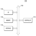
도 9를 참조하면, 본 발명의 실시예에 따른 반도체 장치의 동작 방법 및 반도체 장치가 적용될 수 있는 반도체 시스템(1100)은 컨트롤러(1110), 입출력 장치(1120, I/O), 기억 장치(1130, memory device), 인터페이스(1140) 및 버스(1150, bus)를 포함할 수 있다. 컨트롤러(1110), 입출력 장치(1120), 기억 장치(1130) 및/또는 인터페이스(1140)는 버스(1150)를 통하여 서로 결합될 수 있다. 버스(1150)는 데이터들이 이동되는 통로(path)에 해당한다.Referring to FIG. 9 , a method of operating a semiconductor device and a
컨트롤러(1110)는 마이크로프로세서, 디지털 신호 프로세스, 마이크로컨트롤러, 및 이들과 유사한 기능을 수행할 수 있는 논리 소자들 중에서 적어도 하나를 포함할 수 있다. 입출력 장치(1120)는 키패드(keypad), 키보드 및 디스플레이 장치등을 포함할 수 있다. 기억 장치(1130)는 데이터 및/또는 명령어등을 저장할 수 있다. 인터페이스(1140)는 통신 네트워크로 데이터를 전송하거나 통신 네트워크로부터 데이터를 수신하는 기능을 수행할 수 있다. 인터페이스(1140)는 유선 또는 무선 형태일 수 있다. 예컨대, 인터페이스(1140)는 안테나 또는 유무선 트랜시버등을 포함할 수 있다. The
도시하지 않았지만, 반도체 시스템(1100)은 컨트롤러(1110)의 동작을 향상시키기 위한 동작 메모리로서, 고속의 디램 및/또는 에스램 등을 더 포함할 수도 있다. Although not shown, the
또한, 앞서 설명한 본 발명의 실시예에 따른 프로세서는, 기억 장치(1130) 내에 제공되거나, 컨트롤러(1110), 입출력 장치(1120, I/O) 등의 일부로 제공될 수 있다.In addition, the processor according to the embodiment of the present invention described above may be provided in the
반도체 시스템(1100)은 개인 휴대용 정보 단말기(PDA, personal digital assistant) 포터블 컴퓨터(portable computer), 웹 타블렛(web tablet), 무선 전화기(wireless phone), 모바일 폰(mobile phone), 디지털 뮤직 플레이어(digital music player), 메모리 카드(memory card), 또는 정보를 무선환경에서 송신 및/또는 수신할 수 있는 모든 전자 제품에 적용될 수 있다. The
도 10 내지 도 12는 본 발명의 몇몇 실시예들에 따른 반도체 장치의 동작 방법 및 반도체 장치를 적용할 수 있는 예시적인 반도체 시스템들이다.10 to 12 are exemplary semiconductor systems to which a method of operating a semiconductor device and a semiconductor device according to some embodiments of the present invention may be applied.
도 10은 태블릿 PC(1200)을 도시한 도면이고, 도 11은 노트북(1300)을 도시한 도면이며, 도 12는 스마트폰(1400)을 도시한 것이다. 본 발명의 실시예에 따른 프로세서 중 적어도 하나는 이러한 태블릿 PC(1200), 노트북(1300), 스마트폰(1400) 등에 사용될 수 있다. FIG. 10 shows a
또한, 본 발명의 몇몇 실시예들에 따라 제조된 반도체 장치는, 예시하지 않는 다른 집적 회로 장치에도 적용될 수 있음은 해당 기술 분야의 통상의 기술자에게 자명하다. In addition, it is apparent to those skilled in the art that semiconductor devices manufactured according to some embodiments of the present invention may be applied to other integrated circuit devices not illustrated.
즉, 이상에서는 본 실시예에 따른 반도체 시스템의 예로, 태블릿 PC(1200), 노트북(1300), 및 스마트폰(1400)만을 들었으나, 본 실시예에 따른 반도체 시스템의 예가 이에 제한되는 것은 아니다. That is, in the foregoing, only the
본 발명의 몇몇 실시예에서, 반도체 시스템은, 컴퓨터, UMPC (Ultra Mobile PC), 워크스테이션, 넷북(net-book), PDA (Personal Digital Assistants), 포터블(portable) 컴퓨터, 무선 전화기(wireless phone), 모바일 폰(mobile phone), e-북(e-book), PMP(portable multimedia player), 휴대용 게임기, 네비게이션(navigation) 장치, 블랙박스(black box), 디지털 카메라(digital camera), 3차원 수상기(3-dimensional television), 디지털 음성 녹음기(digital audio recorder), 디지털 음성 재생기(digital audio player), 디지털 영상 녹화기(digital picture recorder), 디지털 영상 재생기(digital picture player), 디지털 동영상 녹화기(digital video recorder), 디지털 동영상 재생기(digital video player) 등으로 구현될 수도 있다.In some embodiments of the present invention, the semiconductor system may be used in a computer, an ultra mobile PC (UMPC), a workstation, a net-book, a personal digital assistant (PDA), a portable computer, or a wireless phone. , mobile phone, e-book, portable multimedia player (PMP), portable game machine, navigation device, black box, digital camera, 3D receiver (3-dimensional television), digital audio recorder, digital audio player, digital picture recorder, digital picture player, digital video recorder ), a digital video player, and the like.
이상 첨부된 도면을 참조하여 본 발명의 실시예들을 설명하였으나, 본 발명은 상기 실시예들에 한정되는 것이 아니라 서로 다른 다양한 형태로 제조될 수 있으며, 본 발명이 속하는 기술분야에서 통상의 지식을 가진 자는 본 발명의 기술적 사상이나 필수적인 특징을 변경하지 않고서 다른 구체적인 형태로 실시될 수 있다는 것을 이해할 수 있을 것이다. 그러므로 이상에서 기술한 실시예들은 모든 면에서 예시적인 것이며 한정적이 아닌 것으로 이해해야만 한다.Although the embodiments of the present invention have been described with reference to the accompanying drawings, the present invention is not limited to the above embodiments and can be manufactured in a variety of different forms, and those skilled in the art in the art to which the present invention belongs A person will understand that the present invention may be embodied in other specific forms without changing the technical spirit or essential features. Therefore, the embodiments described above should be understood as illustrative in all respects and not limiting.
100: 반도체 장치 110, 112: IP 블록
114: 메모리 컨트롤러 130: 온 칩 인터커넥트
200: 모니터링 장치 210: 설정 모듈
220: 필터링 모듈 230: MO 카운터
240: RO 카운터 250: 제어 모듈
260: 레이턴시 카운터 270: 트랙 ID 설정 모듈
300: 메모리 장치100:
114: memory controller 130: on-chip interconnect
200: monitoring device 210: setting module
220: filtering module 230: MO counter
240: RO counter 250: control module
260: latency counter 270: track ID setting module
300: memory device
Claims (20)
상기 복수의 요청 패킷 중 미리 설정된 식별 정보에 부합하는 타겟 요청 패킷을 검출하고,
상기 타겟 요청 패킷과, 상기 복수의 응답 패킷 중 상기 식별 정보에 부합하는 타겟 응답 패킷을 포함하는 트랜잭션(transaction)의 레이턴시(latency)를 측정하기 위한 레이턴시 카운터(latency counter)의 동작을 시작하고,
상기 복수의 응답 패킷 중 상기 타겟 응답 패킷을 검출하고,
상기 레이턴시 카운터의 동작을 중지하고,
상기 레이턴시 카운터로부터 상기 트랜잭션의 레이턴시 값을 획득하고,
MO 카운터(Multiple Outstanding Counter)를 이용하여, 상기 복수의 요청 패킷 중 대응하는 응답 패킷이 아직 검출되지 않은 요청 패킷의 개수를 카운트하고,
RO 카운터(Response Ordering Counter)를 이용하여, 상기 복수의 요청 패킷 중 대응하는 응답 패킷이 검출되었는지 여부를 결정하는 것을 포함하는 반도체 장치의 동작 방법.monitoring a plurality of request packets and a plurality of response packets transmitted between a master device and a slave device;
Detecting a target request packet matching preset identification information among the plurality of request packets;
Starting an operation of a latency counter for measuring latency of a transaction including the target request packet and a target response packet matching the identification information among the plurality of response packets;
Detecting the target response packet among the plurality of response packets;
Stop the operation of the latency counter;
obtaining a latency value of the transaction from the latency counter;
Counting the number of request packets for which a corresponding response packet has not yet been detected among the plurality of request packets by using a multiple outstanding counter (MO counter);
and determining whether a corresponding response packet among the plurality of request packets is detected by using a response ordering counter (RO counter).
상기 레이턴시 카운터의 동작을 시작하는 것은, 상기 MO 카운터의 MO 카운트 값을 상기 RO 카운터의 초기 값으로 설정하는 것을 포함하는 반도체 장치의 동작 방법.According to claim 1,
The method of claim 1 , wherein starting the operation of the latency counter includes setting an MO count value of the MO counter to an initial value of the RO counter.
상기 RO 카운터의 RO 카운트 값은 상기 복수의 요청 패킷 중 대응하는 응답 패킷이 검출될 때마다 감소하고,
상기 레이턴시 카운터의 동작을 중지하는 것은, 상기 RO 카운터의 RO 카운트 값이 0이 되면 상기 레이턴시 카운터의 동작을 중지하는 것을 포함하는 반도체 장치의 동작 방법.According to claim 1,
The RO count value of the RO counter decreases whenever a corresponding response packet is detected among the plurality of request packets;
The stopping of the operation of the latency counter includes stopping the operation of the latency counter when an RO count value of the RO counter becomes 0.
상기 미리 설정된 식별 정보는 트랜잭션 ID 정보 및 트랜잭션 속성(attribute) 정보 중 적어도 하나를 포함하는 반도체 장치의 동작 방법.According to claim 1,
The preset identification information includes at least one of transaction ID information and transaction attribute information.
상기 식별 정보로부터 현재 트랙 ID(current-tracked ID) 정보를 설정하는 것을 더 포함하고,
상기 타겟 요청 패킷을 검출하는 것은,
상기 마스터 디바이스와 상기 슬레이브 디바이스 사이에 형성된 채널의 상태를 결정하고,
상기 채널이 아이들(idle) 상태인 경우, 상기 식별 정보에 부합하는 타겟 요청 패킷을 검출하고,
상기 채널이 비지(busy) 상태인 경우, 상기 현재 트랙 ID 정보에 부합하는 타겟 요청 패킷을 검출하는 것을 포함하는 반도체 장치의 동작 방법.According to claim 1,
Further comprising setting current-tracked ID (ID) information from the identification information;
Detecting the target request packet,
determining a state of a channel formed between the master device and the slave device;
When the channel is in an idle state, detecting a target request packet matching the identification information;
and detecting a target request packet matching the current track ID information when the channel is in a busy state.
상기 채널이 아이들 상태에서 비지 상태로 변경되는 경우, 상기 현재 트랙 ID를 업데이트하는 것을 포함하는 반도체 장치의 동작 방법.According to claim 7,
and updating the current track ID when the channel is changed from an idle state to a busy state.
상기 트랜잭션은 제1 트랜잭션 및 상기 제1 트랜잭션과 다른 제2 트랜잭션을 포함하고,
상기 트랜잭션의 레이턴시 값을 획득하는 것은, 상기 제1 트랜잭션의 제1 레이턴시 값 및 상기 제2 트랜잭션의 제2 레이턴시 값을 획득하는 것을 포함하고,
상기 제1 레이턴시 값 및 상기 제2 레이턴시 값으로부터 평균 레이턴시(average latency) 및 피크 레이턴시(peak latency)를 연산하는 것을 더 포함하는 반도체 장치의 동작 방법.According to claim 1,
the transaction includes a first transaction and a second transaction different from the first transaction;
Acquiring the latency value of the transaction includes obtaining a first latency value of the first transaction and a second latency value of the second transaction;
The method of operating the semiconductor device further comprising calculating an average latency and a peak latency from the first latency value and the second latency value.
상기 평균 레이턴시 및 상기 피크 레이턴시를 이용하여 상기 마스터 디바이스와 상기 슬레이브 디바이스 사이에 형성된 채널(channel)을 디버깅하는 것을 더 포함하는 반도체 장치의 동작 방법.According to claim 9,
The method of operating a semiconductor device further comprising debugging a channel formed between the master device and the slave device using the average latency and the peak latency.
상기 평균 레이턴시 및 상기 피크 레이턴시를 이용하여 상기 마스터 디바이스와 상기 슬레이브 디바이스 사이에 형성된 채널(channel)의 QoS(Quality of Service)를 제어하는 것을 더 포함하는 반도체 장치의 동작 방법.According to claim 9,
The method of operating the semiconductor device further comprising controlling a quality of service (QoS) of a channel formed between the master device and the slave device using the average latency and the peak latency.
상기 시스템 온 칩 외부로부터 미리 설정된 제1 식별 정보 및 제2 식별 정보를 입력받고,
레이턴시 카운터(latency counter)를 이용하여 상기 복수의 트랜잭션 중 상기 제1 식별 정보에 부합하는 제1 트랜잭션의 레이턴시를 측정하고,
상기 레이턴시 카운터를 이용하여 상기 복수의 트랜잭션 중 상기 제2 식별 정보에 부합하는 제2 트랜잭션의 레이턴시를 측정하고,
상기 제1 트랜잭션 및 상기 제2 트랜잭션의 레이턴시로부터 평균 레이턴시(average latency) 및 피크 레이턴시(peak latency)를 연산하고,
MO 카운터(Multiple Outstanding Counter)를 이용하여, 상기 복수의 요청 패킷 중 대응하는 응답 패킷이 아직 검출되지 않은 요청 패킷의 개수를 카운트하고,
RO 카운터(Response Ordering Counter)를 이용하여, 상기 복수의 요청 패킷 중 대응하는 응답 패킷이 검출되었는지 여부를 결정하는 것을 포함하는 반도체 장치의 동작 방법.A plurality of transactions between a first IP block (Intellectual Property Block) and a second IP block provided in a System-on-Chip (SoC) are monitored, and the plurality of transactions include a plurality of request packets and a plurality of contain a response packet;
Receiving preset first identification information and second identification information from the outside of the system-on-chip;
Measuring the latency of a first transaction that matches the first identification information among the plurality of transactions using a latency counter;
Measuring latency of a second transaction that matches the second identification information among the plurality of transactions using the latency counter;
Calculate an average latency and a peak latency from the latencies of the first transaction and the second transaction;
Counting the number of request packets for which a corresponding response packet has not yet been detected among the plurality of request packets by using a multiple outstanding counter (MO counter);
and determining whether a corresponding response packet among the plurality of request packets is detected by using a response ordering counter (RO counter).
외부로부터 상기 미리 설정된 식별 정보를 수신하여 상기 필터링 모듈에 제공하는 설정 모듈;
상기 타겟 요청 패킷과, 상기 복수의 응답 패킷 중 상기 식별 정보에 부합하는 타겟 응답 패킷을 포함하는 트랜잭션(transaction)의 레이턴시(latency)를 측정하기 위한 레이턴시 카운터(latency counter);
상기 레이턴시 카운터 동작을 제어하고, 상기 복수의 응답 패킷 중 상기 타겟 응답 패킷을 검출하는 제어 모듈;
상기 복수의 요청 패킷 중 대응하는 응답 패킷이 아직 검출되지 않은 요청 패킷의 개수를 카운트하는 MO 카운터(Multiple Outstanding Counter); 및
상기 복수의 요청 패킷 중 대응하는 응답 패킷이 검출되었는지 여부를 결정하는 RO 카운터(Response Ordering Counter)를 포함하는 반도체 장치.A filtering module for detecting a target request packet matching preset identification information among a plurality of request packets transmitted between a master device and a slave device;
a setting module receiving the preset identification information from the outside and providing the received identification information to the filtering module;
a latency counter for measuring latency of a transaction including the target request packet and a target response packet matching the identification information among the plurality of response packets;
a control module which controls an operation of the latency counter and detects the target response packet among the plurality of response packets;
an MO counter (Multiple Outstanding Counter) counting the number of request packets for which a corresponding response packet has not yet been detected among the plurality of request packets; and
and a response ordering counter (RO) configured to determine whether a corresponding response packet among the plurality of request packets is detected.
상기 RO 카운터는 상기 MO 카운터로부터 MO 카운트 값을 수신하고, 상기 MO 카운트 값을 상기 RO 카운터의 초기 값으로 설정하는 반도체 장치.According to claim 13,
The RO counter receives an MO count value from the MO counter and sets the MO count value as an initial value of the RO counter.
상기 RO 카운터는 상기 복수의 요청 패킷 중 대응하는 응답 패킷이 검출될 때마다 RO 카운트 값을 감소시키고,
상기 제어 모듈은, 상기 RO 카운트 값이 0이 되면 상기 레이턴시 카운터의 동작을 중지하는 반도체 장치.According to claim 13,
The RO counter decreases an RO count value whenever a corresponding response packet among the plurality of request packets is detected;
The control module stops the operation of the latency counter when the RO count value becomes 0.
상기 식별 정보로부터 현재 트랙 ID(current-tracked ID) 정보를 설정하는 트랙 ID 설정 모듈을 더 포함하고,
상기 필터링 모듈은,
상기 마스터 디바이스와 상기 슬레이브 디바이스 사이에 형성된 채널의 상태를 결정하고,
상기 채널이 아이들(idle) 상태인 경우, 상기 식별 정보에 부합하는 타겟 요청 패킷을 검출하고,
상기 채널이 비지(busy) 상태인 경우, 상기 현재 트랙 ID 정보에 부합하는 타겟 요청 패킷을 검출하는 반도체 장치.According to claim 13,
a track ID setting module configured to set current-tracked ID information from the identification information;
The filtering module,
determining a state of a channel formed between the master device and the slave device;
When the channel is in an idle state, detecting a target request packet matching the identification information;
and detecting a target request packet matching the current track ID information when the channel is in a busy state.
상기 트랙 ID 설정 모듈은, 상기 채널이 아이들 상태에서 비지 상태로 변경되는 경우, 상기 현재 트랙 ID를 업데이트하는 것을 포함하는 반도체 장치.According to claim 18,
and the track ID setting module updates the current track ID when the channel is changed from an idle state to a busy state.
상기 미리 설정된 식별 정보는 트랜잭션 ID 정보 및 트랜잭션 속성(attribute) 정보 중 적어도 하나를 포함하는 반도체 장치.According to claim 13,
The preset identification information includes at least one of transaction ID information and transaction attribute information.
Priority Applications (5)
| Application Number | Priority Date | Filing Date | Title |
|---|---|---|---|
| KR1020160014250A KR102510900B1 (en) | 2016-02-04 | 2016-02-04 | Semiconductor device and method for operating semiconductor device |
| CN201710063623.7A CN107085561B (en) | 2016-02-04 | 2017-02-03 | Semiconductor device and method of operating the same |
| US15/423,628 US10379749B2 (en) | 2016-02-04 | 2017-02-03 | Semiconductor device and operating method thereof |
| TW106103623A TWI747878B (en) | 2016-02-04 | 2017-02-03 | Semiconductor device and operating method thereof |
| US16/503,200 US10564855B2 (en) | 2016-02-04 | 2019-07-03 | Semiconductor device and operating method thereof |
Applications Claiming Priority (1)
| Application Number | Priority Date | Filing Date | Title |
|---|---|---|---|
| KR1020160014250A KR102510900B1 (en) | 2016-02-04 | 2016-02-04 | Semiconductor device and method for operating semiconductor device |
Publications (2)
| Publication Number | Publication Date |
|---|---|
| KR20170092951A KR20170092951A (en) | 2017-08-14 |
| KR102510900B1 true KR102510900B1 (en) | 2023-03-15 |
Family
ID=59498243
Family Applications (1)
| Application Number | Title | Priority Date | Filing Date |
|---|---|---|---|
| KR1020160014250A Active KR102510900B1 (en) | 2016-02-04 | 2016-02-04 | Semiconductor device and method for operating semiconductor device |
Country Status (4)
| Country | Link |
|---|---|
| US (2) | US10379749B2 (en) |
| KR (1) | KR102510900B1 (en) |
| CN (1) | CN107085561B (en) |
| TW (1) | TWI747878B (en) |
Families Citing this family (6)
| Publication number | Priority date | Publication date | Assignee | Title |
|---|---|---|---|---|
| KR102510900B1 (en) * | 2016-02-04 | 2023-03-15 | 삼성전자주식회사 | Semiconductor device and method for operating semiconductor device |
| KR102246469B1 (en) | 2017-07-21 | 2021-05-03 | 한국전자통신연구원 | Reversible electrochemical mirror |
| CN108762967B (en) * | 2018-05-30 | 2021-08-24 | 宁波市标准化研究院 | Software watchdog implementation method for monitoring Web service in Linux system |
| US11042326B2 (en) | 2018-12-13 | 2021-06-22 | SK Hynix Inc. | Data storage device and operating method thereof |
| US11237760B2 (en) | 2019-12-19 | 2022-02-01 | Western Digital Technologies, Inc. | Measuring performance metrics for data storage devices |
| KR102733465B1 (en) * | 2023-12-04 | 2024-11-25 | 리벨리온 주식회사 | Electronic device having a plurality of chiplets |
Family Cites Families (25)
| Publication number | Priority date | Publication date | Assignee | Title |
|---|---|---|---|---|
| US5919268A (en) | 1997-09-09 | 1999-07-06 | Ncr Corporation | System for determining the average latency of pending pipelined or split transaction requests through using two counters and logic divider |
| US6038606A (en) * | 1997-11-25 | 2000-03-14 | International Business Machines Corp. | Method and apparatus for scheduling packet acknowledgements |
| US6775640B1 (en) | 2000-04-28 | 2004-08-10 | Hewlett-Packard Development Company, L.P. | Performance adder for tracking occurrence of events within a circuit |
| JP2002117700A (en) | 2000-10-04 | 2002-04-19 | Mitsubishi Electric Corp | Semiconductor integrated circuit device having delay time measuring circuit |
| US6937961B2 (en) * | 2002-09-26 | 2005-08-30 | Freescale Semiconductor, Inc. | Performance monitor and method therefor |
| CN100514926C (en) * | 2004-09-28 | 2009-07-15 | 松下电器产业株式会社 | Wireless transmission system, wireless station used therein and method used therefor |
| US7565580B2 (en) * | 2005-08-10 | 2009-07-21 | Qlogic, Corporation | Method and system for testing network device logic |
| CN101163051A (en) * | 2006-10-13 | 2008-04-16 | 鸿富锦精密工业(深圳)有限公司 | Network card transmission speed test system and method |
| US8179872B2 (en) * | 2007-05-09 | 2012-05-15 | Research In Motion Limited | Wireless router system and method |
| JP5119994B2 (en) * | 2008-03-14 | 2013-01-16 | 富士通株式会社 | Performance monitoring program, performance monitoring method, performance monitoring device |
| US8032329B2 (en) | 2008-09-04 | 2011-10-04 | Sonics, Inc. | Method and system to monitor, debug, and analyze performance of an electronic design |
| US8489791B2 (en) | 2010-03-12 | 2013-07-16 | Lsi Corporation | Processor bus bridge security feature for network processors or the like |
| US8638792B2 (en) * | 2010-01-22 | 2014-01-28 | Synopsys, Inc. | Packet switch based logic replication |
| KR101855399B1 (en) | 2011-03-24 | 2018-05-09 | 삼성전자주식회사 | System on chip improving data traffic and operating method thereof |
| US20120331034A1 (en) | 2011-06-22 | 2012-12-27 | Alain Fawaz | Latency Probe |
| CN104285190A (en) * | 2012-03-26 | 2015-01-14 | 西门子公司 | Failsafe Discovery and Address Assignment |
| GB2490390B (en) | 2012-03-29 | 2014-01-29 | Renesas Mobile Corp | Method, apparatus and computer program for latency measurement |
| WO2014094237A1 (en) * | 2012-12-18 | 2014-06-26 | Intel Corporation | Techniques associated with server transaction latency information |
| KR101726743B1 (en) * | 2013-01-08 | 2017-04-13 | 후지 덴키 가부시키가이샤 | Control system, master programmable controller, slave programmable controller, and control method |
| JP6458002B2 (en) * | 2014-02-27 | 2019-01-30 | 株式会社サイバー・ソリューションズ | Remote / passive performance monitoring system |
| US10250474B2 (en) | 2014-03-31 | 2019-04-02 | Cisco Technology, Inc. | Calculating latency in computer networks |
| US9506982B2 (en) * | 2014-11-14 | 2016-11-29 | Cavium, Inc. | Testbench builder, system, device and method including a generic monitor and transporter |
| JP6554981B2 (en) * | 2015-08-03 | 2019-08-07 | セイコーエプソン株式会社 | Diagnostic server, diagnostic system, diagnostic method, diagnostic program, recording medium |
| KR102510900B1 (en) * | 2016-02-04 | 2023-03-15 | 삼성전자주식회사 | Semiconductor device and method for operating semiconductor device |
| KR102440948B1 (en) * | 2016-02-11 | 2022-09-05 | 삼성전자주식회사 | Semiconductor device and method for operating semiconductor device |
-
2016
- 2016-02-04 KR KR1020160014250A patent/KR102510900B1/en active Active
-
2017
- 2017-02-03 CN CN201710063623.7A patent/CN107085561B/en active Active
- 2017-02-03 TW TW106103623A patent/TWI747878B/en active
- 2017-02-03 US US15/423,628 patent/US10379749B2/en active Active
-
2019
- 2019-07-03 US US16/503,200 patent/US10564855B2/en active Active
Non-Patent Citations (2)
| Title |
|---|
| Christian Herber 외 2 명, 'Design and Evaluation of a Low-Latency AVB Ethernet Endpoint based on ARM SoC,' IEEE, (2015.08.24.)* |
| Christian Herber 외 2 명, 'Design and Evaluation of a Low-Latency AVB Ethernet Endpoint based on ARM SoC,' IEEE, 2015.08.24.)* |
Also Published As
| Publication number | Publication date |
|---|---|
| TWI747878B (en) | 2021-12-01 |
| US10564855B2 (en) | 2020-02-18 |
| US20190324660A1 (en) | 2019-10-24 |
| CN107085561A (en) | 2017-08-22 |
| TW201732608A (en) | 2017-09-16 |
| US10379749B2 (en) | 2019-08-13 |
| US20170228169A1 (en) | 2017-08-10 |
| KR20170092951A (en) | 2017-08-14 |
| CN107085561B (en) | 2022-01-18 |
Similar Documents
| Publication | Publication Date | Title |
|---|---|---|
| KR102510900B1 (en) | Semiconductor device and method for operating semiconductor device | |
| CN101112112B (en) | Method of measuring distance between two radio communication devices and device suitable for carrying out the method | |
| US12316520B2 (en) | Semiconductor device and operating method thereof | |
| US20100318706A1 (en) | Bus arbitration circuit and bus arbitration method | |
| CN110072219A (en) | For wirelessly close to electronic equipment, method and the computer-readable medium of pairing | |
| TW200421104A (en) | Performance monitor and method therefor | |
| US10530562B2 (en) | Correlating local time counts of first and second integrated circuits | |
| CN112765082A (en) | Multi-host arbitration method and device and readable storage medium | |
| TWI516942B (en) | Assigning addresses to devices on an interconnect | |
| KR20160047484A (en) | Method to minimize the number of irq lines from peripherals to one wire | |
| US10671722B2 (en) | Mechanism for throttling untrusted interconnect agents | |
| JP6531593B2 (en) | Communication method, communication program and information processing apparatus | |
| US10452134B2 (en) | Automated peripheral device handoff based on eye tracking | |
| CN110636522B (en) | A method and device for determining the coverage quality of a communication network | |
| WO2013144900A1 (en) | Method, apparatus and computer program for latency measurement | |
| CN104731524B (en) | The method that capacity register is set | |
| WO2018187313A1 (en) | Aggregating cache maintenance instructions in processor-based devices | |
| CN120050133A (en) | Data polling transmission method, device and equipment based on level signals | |
| TWM614918U (en) | Charging device |
Legal Events
| Date | Code | Title | Description |
|---|---|---|---|
| PA0109 | Patent application |
Patent event code: PA01091R01D Comment text: Patent Application Patent event date: 20160204 |
|
| PG1501 | Laying open of application | ||
| A201 | Request for examination | ||
| PA0201 | Request for examination |
Patent event code: PA02012R01D Patent event date: 20210113 Comment text: Request for Examination of Application Patent event code: PA02011R01I Patent event date: 20160204 Comment text: Patent Application |
|
| E902 | Notification of reason for refusal | ||
| PE0902 | Notice of grounds for rejection |
Comment text: Notification of reason for refusal Patent event date: 20221129 Patent event code: PE09021S01D |
|
| E701 | Decision to grant or registration of patent right | ||
| PE0701 | Decision of registration |
Patent event code: PE07011S01D Comment text: Decision to Grant Registration Patent event date: 20230206 |
|
| GRNT | Written decision to grant | ||
| PR0701 | Registration of establishment |
Comment text: Registration of Establishment Patent event date: 20230313 Patent event code: PR07011E01D |
|
| PR1002 | Payment of registration fee |
Payment date: 20230313 End annual number: 3 Start annual number: 1 |
|
| PG1601 | Publication of registration |