KR102487514B1 - Organic electro luminescence device - Google Patents
Organic electro luminescence device Download PDFInfo
- Publication number
- KR102487514B1 KR102487514B1 KR1020150181623A KR20150181623A KR102487514B1 KR 102487514 B1 KR102487514 B1 KR 102487514B1 KR 1020150181623 A KR1020150181623 A KR 1020150181623A KR 20150181623 A KR20150181623 A KR 20150181623A KR 102487514 B1 KR102487514 B1 KR 102487514B1
- Authority
- KR
- South Korea
- Prior art keywords
- host
- homo
- lumo
- dopant
- energy level
- Prior art date
- Legal status (The legal status is an assumption and is not a legal conclusion. Google has not performed a legal analysis and makes no representation as to the accuracy of the status listed.)
- Active
Links
Classifications
-
- H01L51/5004—
-
- C—CHEMISTRY; METALLURGY
- C07—ORGANIC CHEMISTRY
- C07D—HETEROCYCLIC COMPOUNDS
- C07D403/00—Heterocyclic compounds containing two or more hetero rings, having nitrogen atoms as the only ring hetero atoms, not provided for by group C07D401/00
- C07D403/02—Heterocyclic compounds containing two or more hetero rings, having nitrogen atoms as the only ring hetero atoms, not provided for by group C07D401/00 containing two hetero rings
- C07D403/10—Heterocyclic compounds containing two or more hetero rings, having nitrogen atoms as the only ring hetero atoms, not provided for by group C07D401/00 containing two hetero rings linked by a carbon chain containing aromatic rings
-
- C—CHEMISTRY; METALLURGY
- C07—ORGANIC CHEMISTRY
- C07D—HETEROCYCLIC COMPOUNDS
- C07D487/00—Heterocyclic compounds containing nitrogen atoms as the only ring hetero atoms in the condensed system, not provided for by groups C07D451/00 - C07D477/00
- C07D487/02—Heterocyclic compounds containing nitrogen atoms as the only ring hetero atoms in the condensed system, not provided for by groups C07D451/00 - C07D477/00 in which the condensed system contains two hetero rings
- C07D487/04—Ortho-condensed systems
-
- C—CHEMISTRY; METALLURGY
- C09—DYES; PAINTS; POLISHES; NATURAL RESINS; ADHESIVES; COMPOSITIONS NOT OTHERWISE PROVIDED FOR; APPLICATIONS OF MATERIALS NOT OTHERWISE PROVIDED FOR
- C09K—MATERIALS FOR MISCELLANEOUS APPLICATIONS, NOT PROVIDED FOR ELSEWHERE
- C09K11/00—Luminescent materials, e.g. electroluminescent or chemiluminescent
- C09K11/06—Luminescent materials, e.g. electroluminescent or chemiluminescent containing organic luminescent materials
-
- H01L51/0072—
-
- H01L51/5012—
-
- H01L51/5024—
-
- H01L51/5056—
-
- H01L51/5072—
-
- H01L51/5088—
-
- C—CHEMISTRY; METALLURGY
- C09—DYES; PAINTS; POLISHES; NATURAL RESINS; ADHESIVES; COMPOSITIONS NOT OTHERWISE PROVIDED FOR; APPLICATIONS OF MATERIALS NOT OTHERWISE PROVIDED FOR
- C09K—MATERIALS FOR MISCELLANEOUS APPLICATIONS, NOT PROVIDED FOR ELSEWHERE
- C09K2211/00—Chemical nature of organic luminescent or tenebrescent compounds
- C09K2211/10—Non-macromolecular compounds
- C09K2211/1018—Heterocyclic compounds
- C09K2211/1025—Heterocyclic compounds characterised by ligands
- C09K2211/1029—Heterocyclic compounds characterised by ligands containing one nitrogen atom as the heteroatom
Landscapes
- Chemical & Material Sciences (AREA)
- Organic Chemistry (AREA)
- Engineering & Computer Science (AREA)
- Materials Engineering (AREA)
- Electroluminescent Light Sources (AREA)
Abstract
본 발명은 양극; 음극; 및 상기 양극과 음극 사이에 개재(介在)된 1층 이상의 유기물층을 포함하며, 상기 1층 이상의 유기물층 중 적어도 하나는 제1 호스트, 제2 호스트 및 도펀트를 포함하는 유기 전계 발광 소자를 제공한다.The present invention is a positive electrode; cathode; and one or more organic material layers interposed between the anode and the cathode, wherein at least one of the one or more organic material layers includes a first host, a second host, and a dopant.
Description
본 발명은 1층 이상의 유기물층을 포함하는 유기 전계 발광 소자에 관한 것이다.The present invention relates to an organic electroluminescent device including one or more organic material layers.
유기 전계 발광 소자의 발광 효율을 높이기 위해서는 색순도 증가와 에너지 전이가 필요한데, 이는 유기 전계 발광 소자에 포함되는 유기물층에 호스트 물질과 도펀트 물질이 혼합된 발광층을 적용함으로써 달성할 수 있다.In order to increase the luminous efficiency of the organic light emitting device, color purity and energy transfer are required, which can be achieved by applying a light emitting layer in which a host material and a dopant material are mixed to an organic material layer included in the organic light emitting device.
상기 도펀트 물질은 유기 물질을 사용하는 형광 도펀트와 인광 도펀트로 나눌 수 있다. 이때, 인광 물질은 이론적으로 형광 물질에 비해 4배까지 발광 효율을 향상시킬 수 있기 때문에 인광 도펀트 뿐만 아니라 인광 호스트에 대한 연구도 다양하게 진행되고 있다.The dopant material may be divided into a fluorescent dopant and a phosphorescent dopant using an organic material. At this time, since phosphorescent materials can theoretically improve luminous efficiency up to 4 times compared to fluorescent materials, researches on phosphorescent dopants as well as phosphorescent hosts are being conducted in various ways.
현재 발광층에 적용되는 인광 도펀트 물질로는 Firpic, Ir(ppy)3, (acac)Ir(btp)2 등과 같은 Ir을 포함하는 금속 착체 화합물이 알려져 있으며, 인광 호스트 물질로는 CBP, mCP가 알려져 있다. 구체적으로, 상기 Firpic을 청색 인광 도펀트로 적용하면서 상기 mCP를 청색 인광 호스트로 적용하거나, 상기 Ir(ppy)3을 녹색 인광 도펀트로 적용하면서 상기 CBP를 녹색 인광 호스트로 적용하는 것이 알려진 바 있다.Metal complex compounds containing Ir such as Firpic, Ir(ppy) 3 , (acac)Ir(btp) 2 , etc. are known as phosphorescent dopant materials currently applied to the light emitting layer, and CBP and mCP are known as phosphorescent host materials. . Specifically, it is known to apply the mCP as a blue phosphorescent host while applying the Firpic as a blue phosphorescent dopant, or to apply the CBP as a green phosphorescent host while applying the Ir(ppy) 3 as a green phosphorescent dopant.
그런데, 인광 도펀트 및 인광 호스트가 적용된 발광층은 삼중항 에너지를 이용하여 발광하기 때문에 밴드 갭이 크고, 전하 캐리어 주입/수송이 용이하면서 엑시톤의 구속력이 큰 인광 물질을 적용하지 않는 한 고효율의 유기 전계 발광 소자를 얻는데 한계가 있다. 따라서, 밴드 갭이 크고 전하 캐리어 주입/수송이 용이하면서 엑시톤의 구속력이 큰 인광 물질이 적용된 발광층을 포함하는 유기 전계 발광 소자의 개발이 요구되고 있다.However, since the light emitting layer to which the phosphorescent dopant and the phosphorescent host are applied emits light using triplet energy, organic electroluminescence with high efficiency is not applied unless a phosphorescent material having a large band gap, easy charge carrier injection/transport, and high exciton binding force is used. There is a limit to obtaining a small element. Therefore, there is a need to develop an organic electroluminescent device including a light emitting layer to which a phosphor having a large band gap, easy charge carrier injection/transport, and high exciton binding force is applied.
본 발명은 상기한 문제점을 해결하기 위해, 구동 전압, 발광 효율 및 수명 등의 특성이 향상되어 고효율을 나타내는 유기 전계 발광 소자를 제공하는 것을 목적으로 한다.In order to solve the above problems, an object of the present invention is to provide an organic electroluminescent device exhibiting high efficiency by improving characteristics such as driving voltage, luminous efficiency and lifetime.
상기한 목적을 달성하기 위해, 본 발명은 양극; 음극; 및 상기 양극과 음극 사이에 개재된 유기물층을 포함하고, 상기 유기물층은 정공 주입층, 정공 수송층, 발광층 및 전자 수송층으로 이루어진 군에서 선택된 1종 이상을 포함하며, 상기 발광층은 제1 호스트, 제2 호스트 및 도펀트를 포함하고, 상기 제1 호스트, 상기 제2 호스트 및 상기 도펀트의 에너지 준위는 하기 관계식을 만족하는 유기 전계 발광 소자를 제공한다. In order to achieve the above object, the present invention is a positive electrode; cathode; and an organic material layer interposed between the anode and the cathode, wherein the organic material layer includes at least one selected from the group consisting of a hole injection layer, a hole transport layer, a light emitting layer, and an electron transport layer, wherein the light emitting layer includes a first host and a second host. and a dopant, wherein energy levels of the first host, the second host, and the dopant satisfy the following relational expression.
HOMOD > HOMO1host > HOMO2host HOMO D > HOMO 1host > HOMO 2host
LUMOD < LUMO2host < LUMO1host LUMO D < LUMO 2host < LUMO 1host
상기 식에서 각각이 의미하는 바는 다음과 같다.In the above formula, each means is as follows.
HOMOD : 도펀트의 HOMO 에너지 준위HOMO D : HOMO energy level of dopant
HOMO1host : 제1 호스트의 HOMO 에너지 준위HOMO 1host : HOMO energy level of the first host
HOMO2host : 제2 호스트의 HOMO 에너지 준위HOMO 2host : HOMO energy level of the second host
LUMOD : 도펀트의 LUMO 에너지 준위LUMO D : LUMO energy level of dopant
LUMO1host : 제1 호스트의 LUMO 에너지 준위LUMO 1host : LUMO energy level of the 1st host
LUMO2host : 제2 호스트의 LUMO 에너지 준위LUMO 2host : LUMO energy level of the 2nd host
본 발명의 유기 전계 발광 소자는 발광층에 전자 전달성(electron dominant) 제1 호스트, 정공 전달성(hole dominant) 제2 호스트 및 도펀트를 포함하기 때문에, 1종의 호스트가 적용된 발광층을 포함하는 종래의 유기 전계 발광 소자에 비해 구동 전압, 발광 효율 및 수명 등의 특성이 더 향상될 수 있다. 따라서, 본 발명의 유기 전계 발광 소자는 고효율을 나타낼 수 있으며, 이러한 유기 전계 발광 소자로 디스플레이 패널을 제조할 경우, 성능 및 수명이 향상된 디스플레이 패널을 제공할 수 있다.Since the organic electroluminescent device of the present invention includes an electron dominant first host, a hole dominant second host, and a dopant in the light emitting layer, a conventional light emitting layer including a light emitting layer to which one kind of host is applied. Compared to organic electroluminescent devices, characteristics such as driving voltage, luminous efficiency, and lifespan may be further improved. Therefore, the organic electroluminescent device of the present invention can exhibit high efficiency, and when a display panel is manufactured using such an organic electroluminescent device, a display panel with improved performance and lifespan can be provided.
이하, 본 발명에 대해 설명한다.Hereinafter, the present invention will be described.
본 발명의 유기 전계 발광 소자는 양극(anode), 음극(cathode), 및 상기 양극과 음극 사이에 개재(介在)된 1층 이상의 유기물층을 포함하고, 상기 유기물층은 정공 주입층, 정공 수송층, 발광층 및 전자 수송층으로 이루어진 군에서 선택된 1종 이상을 포함하며, 상기 발광층은 제1 호스트, 제2 호스트 및 도펀트를 포함하는 것으로, 이에 대해 구체적으로 설명하면 다음과 같다.The organic electroluminescent device of the present invention includes an anode, a cathode, and one or more organic material layers interposed between the anode and the cathode, and the organic material layer includes a hole injection layer, a hole transport layer, a light emitting layer, and It includes at least one selected from the group consisting of an electron transport layer, and the light emitting layer includes a first host, a second host, and a dopant, which will be described in detail as follows.
본 발명의 유기 전계 발광 소자에 포함되는 양극은 정공을 유기물층으로 주입하는 역할을 한다. 이러한 양극에 적용되는 물질은 특별히 한정되지 않으나, 비제한적인 예로, 바나듐, 크롬, 구리, 아연, 금과 같은 금속 또는 이들의 합금; 아연산화물, 인듐산화물, 인듐 주석 산화물(ITO), 인듐 아연 산화물(IZO)과 같은 금속 산화물; ZnO:Al 또는 SnO2:Sb와 같은 금속과 산화물의 조합; 폴리티오펜, 폴리(3-메틸티오펜), 폴리[3,4-(에틸렌-1,2-디옥시)티오펜](PEDT), 폴리피롤, 폴리아닐린 등의 전도성 고분자; 및 카본블랙 등을 들 수 있다. 또한, 양극을 제조하는 방법도 특별히 한정되지 않으나, 비제한적인 예로, 실리콘 웨이퍼, 석영, 유리판, 금속판, 플라스틱 필름 등의 재질로 이루어진 기판 상에 양극 물질을 코팅하는 방법을 들 수 있다.The anode included in the organic electroluminescent device of the present invention serves to inject holes into the organic material layer. Materials applied to the anode are not particularly limited, but include, but are not limited to, metals such as vanadium, chromium, copper, zinc, gold, or alloys thereof; metal oxides such as zinc oxide, indium oxide, indium tin oxide (ITO), and indium zinc oxide (IZO); combinations of metals and oxides such as ZnO:Al or SnO 2 :Sb; conductive polymers such as polythiophene, poly(3-methylthiophene), poly[3,4-(ethylene-1,2-dioxy)thiophene] (PEDT), polypyrrole, and polyaniline; and carbon black. In addition, the method of manufacturing the anode is not particularly limited, but non-limiting examples include a method of coating an anode material on a substrate made of a material such as a silicon wafer, quartz, glass plate, metal plate, or plastic film.
본 발명의 유기 전계 발광 소자에 포함되는 음극은 전자를 유기물층으로 주입하는 역할을 한다. 이러한 음극에 적용되는 물질은 특별히 한정되지 않으나, 비제한적인 예로, 마그네슘, 칼슘, 나트륨, 칼륨, 타이타늄, 인듐, 이트륨, 리튬, 가돌리늄, 알루미늄, 은, 주석, 또는 납과 같은 금속 또는 이들의 합금; 및 LiF/Al 또는 LiO2/Al과 같은 다층 구조 물질 등을 들 수 있다. 또한, 음극을 제조하는 방법도 당업계에 공지된 방법이라면 특별히 한정되지 않는다.The cathode included in the organic electroluminescent device of the present invention serves to inject electrons into the organic material layer. Materials applied to the negative electrode are not particularly limited, but non-limiting examples include metals such as magnesium, calcium, sodium, potassium, titanium, indium, yttrium, lithium, gadolinium, aluminum, silver, tin, or lead, or alloys thereof. ; and multi-layered materials such as LiF/Al or LiO 2 /Al. In addition, a method of manufacturing the negative electrode is not particularly limited as long as it is a method known in the art.
본 발명의 유기 전계 발광 소자에 포함되는 유기물층은 정공 주입층, 정공 수송층, 발광층 및 전자 수송층으로 이루어진 군에서 선택된 1종 이상을 포함하는데, 유기 전계 발광 소자의 특성을 고려할 때, 상기 층들을 모두 포함하는 것이 바람직하다.The organic material layer included in the organic electroluminescent device of the present invention includes at least one selected from the group consisting of a hole injection layer, a hole transport layer, a light emitting layer, and an electron transport layer. Considering the characteristics of the organic electroluminescent device, all of the above layers are included. It is desirable to do
본 발명의 유기물층에 포함되는 정공 주입층과 정공 수송층은 양극에서 주입된 정공을 발광층으로 이동시키는 역할을 한다. 상기 정공 주입층에 적용되는 물질은 특별히 한정되지 않으나, 낮은 전압에서 양극으로부터 정공을 원활히 받을 수 있는 물질로서, HOMO(highest occupied molecular orbital) 값이 양극에 적용되는 물질의 일함수와 주변 유기물층(특히, 발광층)에 적용되는 HOMO 값의 사이인 것이 바람직하다. 구체적으로, 정공 주입층에 적용되는 물질의 비제한적인 예로는 금속 포피린(porphyrine), 올리고티오펜, 아릴아민 계열의 유기물, 헥사니트릴헥사아자트리페닐렌 계열의 유기물, 퀴나크리돈(quinacridone) 계열의 유기물, 페릴렌(perylene) 계열의 유기물, 안트라퀴논 및 폴리아닐린과 폴리티오펜 계열의 전도성 고분자 등을 들 수 있다.The hole injection layer and the hole transport layer included in the organic layer of the present invention serve to move holes injected from the anode to the light emitting layer. The material applied to the hole injection layer is not particularly limited, but is a material that can smoothly receive holes from the anode at a low voltage, and the work function of the material to which the highest occupied molecular orbital (HOMO) value is applied to the anode and the surrounding organic layer (especially , the HOMO value applied to the light emitting layer) is preferably between. Specifically, non-limiting examples of materials applied to the hole injection layer include metal porphyrine, oligothiophene, arylamine-based organic materials, hexanitrilehexaazatriphenylene-based organic materials, and quinacridone-based materials. organic materials, perylene-based organic materials, anthraquinone, and polyaniline- and polythiophene-based conductive polymers.
또한, 상기 정공 수송층에 적용되는 물질도 특별히 한정되지 않으나, 양극이나 정공 주입층으로부터 정공을 수송 받아 발광층으로 이동시킬 수 있는 물질로, 정공의 이동성이 큰 물질인 것이 바람직하다. 구체적으로, 정공 수송층에 적용되는 물질의 비제한적인 예로는 아릴아민 계열의 유기물, 전도성 고분자, 및 공액 부분과 비공액 부분이 함께 있는 블록 공중합체 등을 들 수 있다.In addition, the material applied to the hole transport layer is not particularly limited, but it is preferably a material capable of transporting holes from the anode or the hole injection layer to the light emitting layer, and having high hole mobility. Specifically, non-limiting examples of materials applied to the hole transport layer include arylamine-based organic materials, conductive polymers, and block copolymers having both conjugated and non-conjugated parts.
본 발명의 유기물층에 포함되는 발광층은 정공과 전자가 만나 엑시톤(exciton)이 형성되는 층이다. 구체적으로, 발광층으로 주입된 정공은 제1 호스트의 HOMO 에너지 준위를 이용하고, 발광층으로 주입된 전자는 제2 호스트의 LUMO 에너지 준위를 이용하여 엑시톤을 형성한다. 이러한 본 발명의 발광층은 전자 전달성 제1 호스트, 정공 전달성 제2 호스트 및 도펀트를 포함하며, 상기 제1 호스트, 상기 제2 호스트 및 상기 도펀트는 하기 식을 만족한다.The light emitting layer included in the organic layer of the present invention is a layer in which holes and electrons meet to form excitons. Specifically, holes injected into the light emitting layer use the HOMO energy level of the first host, and electrons injected into the light emitting layer use the LUMO energy level of the second host to form excitons. The light emitting layer of the present invention includes a first electron transporting host, a second hole transporting host, and a dopant, and the first host, the second host, and the dopant satisfy the following equation.
HOMOD > HOMO1host > HOMO2host HOMO D > HOMO 1host > HOMO 2host
LUMOD < LUMO2host < LUMO1host LUMO D < LUMO 2host < LUMO 1host
상기 식에서 각각이 의미하는 바는 다음과 같다.In the above formula, each means is as follows.
HOMOD : 도펀트의 HOMO 에너지 준위HOMO D : HOMO energy level of dopant
HOMO1host : 제1 호스트의 HOMO 에너지 준위HOMO 1host : HOMO energy level of the first host
HOMO2host : 제2 호스트의 HOMO 에너지 준위HOMO 2host : HOMO energy level of the second host
LUMOD : 도펀트의 LUMO 에너지 준위LUMO D : LUMO energy level of dopant
LUMO1host : 제1 호스트의 LUMO 에너지 준위LUMO 1host : LUMO energy level of the 1st host
LUMO2host : 제2 호스트의 LUMO 에너지 준위LUMO 2host : LUMO energy level of the 2nd host
상기 제1 호스트의 HOMO 에너지 준위는 도펀트의 HOMO 에너지 준위보다 낮으면 특별히 한정되지 않으나, 5.0 내지 7.0 eV 인 것이 바람직하다. 또한, 제2 호스트의 HOMO 에너지 준위는 상기 제1 호스트의 HOMO 에너지 준위 보다 낮으면 특별히 한정되지는 않는다. 바람직하게는 HOMO1host와 HOMO2host의 차이가 0.1 내지 0.5 eV 일 수 있다.The HOMO energy level of the first host is not particularly limited as long as it is lower than the HOMO energy level of the dopant, but is preferably 5.0 to 7.0 eV. In addition, the HOMO energy level of the second host is not particularly limited as long as it is lower than the HOMO energy level of the first host. Preferably, the difference between HOMO 1host and HOMO 2host may be 0.1 to 0.5 eV.
상기 제2 호스트의 LUMO 에너지 준위는 도펀트의 LUMO 에너지 준위보다 높으면 특별히 한정되지 않으나, 1.0 내지 3.0 eV 인 것이 바람직하다. 또한, 제1 호스트의 LUMO 에너지 준위는 상기 제2 호스트의 LUMO 에너지 준위 보다 높으면 특별히 한정되지는 않는다. 바람직하게는 LUMO1host와 LUMO2host의 차이가 0.1 내지 0.5 eV 일 수 있다.The LUMO energy level of the second host is not particularly limited as long as it is higher than the LUMO energy level of the dopant, but is preferably 1.0 to 3.0 eV. In addition, the LUMO energy level of the first host is not particularly limited as long as it is higher than the LUMO energy level of the second host. Preferably, the difference between LUMO 1host and LUMO 2host may be 0.1 to 0.5 eV.
상기 도펀트의 HOMO 에너지 준위는 제1 호스트 및 제2 호스트보다 높아, 발광층으로의 정공 주입 효율을 향상시킨다. 이와 같이 정공 주입 효율이 향상되면, 발광층에서의 엑시톤 형성이 원활해지기 때문에 높은 발광 효율을 나타낼 수 있다. The HOMO energy level of the dopant is higher than that of the first host and the second host, thereby improving hole injection efficiency into the light emitting layer. When the hole injection efficiency is improved as described above, excitons are formed smoothly in the light emitting layer, so that high light emitting efficiency can be exhibited.
한편, 상기 제1 호스트 및 제2 호스트의 삼중항 에너지는 도펀트의 삼중항 에너지보다 크면 특별히 한정되지 않으나, 2.0 내지 3.5 eV 인 것이 바람직하다. 호스트에서 도펀트로의 에너지 전이가 용이하게 이루어지기 위해서 인광 발광층에 있는 제1 호스트 및 제2 호스트 물질은 단일항과 삼중항 에너지 레벨이 도펀트 물질의 단일항과 삼중항 에너지보다 높아야 한다. 이는 도펀트의 삼중항에 있는 엑시톤이 다시 호스트로 역전이 되는 현상을 막고, 유기 전계 발광 소자의 발광 효율, 구동 전압 및 수명 등을 더 향상시킬 수 있기 때문이다.Meanwhile, the triplet energy of the first host and the second host is not particularly limited as long as it is greater than the triplet energy of the dopant, but is preferably 2.0 to 3.5 eV. In order to facilitate energy transfer from the host to the dopant, the singlet and triplet energies of the first host and the second host materials in the phosphorescent light emitting layer should be higher than singlet and triplet energies of the dopant material. This is because excitons in the triplet of the dopant are prevented from being reversed back to the host, and the light emitting efficiency, driving voltage, lifespan, and the like of the organic light emitting device can be further improved.
구체적으로, 발광층이 적색 인광일 경우 제1 호스트 및 제2 호스트의 삼중항 에너지는 2.0 eV 이상인 것이 바람직하고, 발광층이 녹색 인광일 경우 제1 호스트 및 제2 호스트의 삼중항 에너지는 2.3 eV 이상인 것이 바람직하며, 발광층이 청색 인광일 경우 제1 호스트 및 제2 호스트의 삼중항 에너지는 2.5 eV 이상인 것이 바람직하다. 또한, 제1 호스트 및 제2 호스트의 삼중항 에너지가 각각 3.5 eV를 초과할 경우, 구동 전압이 상승할 수 있으므로, 제1 호스트 및 제2 호스트의 삼중항 에너지는 각각 2.0 내지 3.5 eV 인 것이 바람직하다.Specifically, when the light emitting layer is red phosphorescent, the triplet energies of the first host and the second host are preferably 2.0 eV or more, and when the light emitting layer is green phosphorescent, the triplet energies of the first host and the second host are 2.3 eV or more. Preferably, when the light emitting layer is blue phosphorescent, the triplet energies of the first host and the second host are preferably 2.5 eV or more. In addition, when the triplet energies of the first host and the second host each exceed 3.5 eV, the driving voltage may increase. Therefore, the triplet energies of the first host and the second host are preferably 2.0 to 3.5 eV, respectively. Do.
여기서, 삼중항 에너지는 기저 상태와 삼중항 상태의 에너지 차이를 의미한다. Here, the triplet energy means the energy difference between the ground state and the triplet state.
상기 제1 호스트의 전자 이동도는 상온에서 1X10⁻⁶ cm2/V·s 이상이고, 상기 제2 호스트의 정공 이동도는 상온에서 1X10⁻⁶ cm2/V·s 이상인 것이 바람직하다. 제1 호스트의 전자 이동도와 제2 호스트의 정공 이동도가 상기 범위일 경우, 발광층으로 전자와 정공을 효과적으로 주입시킬 수 있기 때문이다.Preferably, the electron mobility of the first host is 1X10 -6 cm 2 /V·s or more at room temperature, and the hole mobility of the second host is 1X10 -6 cm 2 /V·s or more at room temperature. This is because electrons and holes can be effectively injected into the light emitting layer when the electron mobility of the first host and the hole mobility of the second host are within the above ranges.
이러한 발광층에 포함되는 제1 호스트 및 제2 호스트는 각각 트리페닐렌계 화합물, 디벤조퓨란계 화합물, 디벤조싸이오펜계 화합물, 아제핀계 화합물, 카바졸계 화합물, 포스핀 옥사이드(Phosphine oxide)계 화합물 및 함질소 복소환계 화합물(예컨대, 피리미딘계 화합물)로 이루어진 군에서 선택되는 것이 바람직하다. The first host and the second host included in the light emitting layer are triphenylene-based compounds, dibenzofuran-based compounds, dibenzothiophene-based compounds, azepine-based compounds, carbazole-based compounds, phosphine oxide-based compounds, and It is preferably selected from the group consisting of nitrogen-containing heterocyclic compounds (eg, pyrimidine compounds).
상기 트리페닐렌계 화합물, 디벤조퓨란계 화합물, 디벤조싸이오펜계 화합물, 아제핀계 화합물 및 카바졸계 화합물은 각각 삼중항 에너지가 3.0 eV 이상이기 때문에, 적색 및 녹색 인광 호스트뿐만 아니라 청색 인광 호스트로도 적용될 수 있다. 또한, 열적 안정성이 매우 우수하여 소자의 안정성도 향상시킬 수 있다. 이러한 트리페닐렌계 화합물, 디벤조퓨란계 화합물, 디벤조싸이오펜계 화합물, 아제핀계 화합물 및 카바졸계 화합물의 구체적인 예로는 하기 H1 내지 H25로 표시되는 화합물을 들 수 있으나, 이에 한정되는 것은 아니다.Since the triphenylene-based compound, the dibenzofuran-based compound, the dibenzothiophene-based compound, the azepine-based compound, and the carbazole-based compound each have a triplet energy of 3.0 eV or more, they can be used as a blue phosphorescent host as well as a red and green phosphorescent host. can be applied In addition, since the thermal stability is very excellent, the stability of the device can be improved. Specific examples of the triphenylene-based compound, dibenzofuran-based compound, dibenzothiophene-based compound, azepine-based compound, and carbazole-based compound include, but are not limited to, compounds represented by H1 to H25 below.
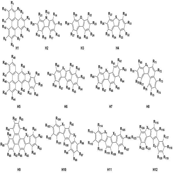

상기 H1 내지 H25에서In the above H1 to H25
X1은 NAr1, O, 또는 S이며, X 1 is NAr 1 , O, or S;
X2는 NAr2, O, S, 또는 CR248R249이며,X 2 is NAr 2 , O, S, or CR 248 R 249 ;
상기 X1 및 X2는 동일하거나 상이하며, 하나 이상은 NAr1이고,X 1 and X 2 are the same or different, and at least one is NAr 1 ;
상기 Ar1 및 Ar2는 각각 독립적으로 C6 내지 C40의 아릴기, 또는 핵원자수 5 내지 40의 헤테로아릴기이며,Ar 1 and Ar 2 are each independently a C 6 to C 40 aryl group or a heteroaryl group having 5 to 40 nuclear atoms,
R1 내지 R249는 각각 독립적으로 수소, C1 내지 C40의 알킬기, C6 내지 C40의 아릴기 및 핵원자수 5 내지 40의 헤테로아릴기이거나, 인접한 기와 결합하여 축합 고리(구체적으로, 축합 방향족 고리, 축합 헤테로방향족 고리)를 형성하고, R 1 to R 249 are each independently hydrogen, a C 1 to C 40 alkyl group, a C 6 to C 40 aryl group, and a heteroaryl group having 5 to 40 nuclear atoms, or combined with adjacent groups to form a condensed ring (specifically, condensed aromatic rings, condensed heteroaromatic rings),
상기 Ar1, Ar2의 아릴기, 헤테로아릴기 및 상기 R1 내지 R249의 알킬기, 아릴기, 헤테로아릴기는 각각 독립적으로 치환 또는 비치환된 C6 내지 C40의 아릴기, 또는 치환 또는 비치환된 핵원자수 5 내지 40의 헤테로아릴기로 치환 또는 비치환된다.The Ar 1 and Ar 2 aryl groups, heteroaryl groups, and the R 1 to R 249 alkyl, aryl and heteroaryl groups are each independently a substituted or unsubstituted C 6 to C 40 aryl group, or a substituted or unsubstituted It is substituted or unsubstituted with a ringed heteroaryl group having 5 to 40 nuclear atoms.
한편, 상기 포스핀 옥사이드(Phosphine oxide)계 화합물도 포스핀 옥사이드기로 인해 π-π conjugation 방해를 받아 밴드 갭이 크고, 삼중항 에너지가 3.0 eV 이상이기 때문에 녹색/적색/청색 인광 호스트로 적용할 수 있다. 또한, 전자 수송 특성이 우수하기 때문에 유기 전계 발광 소자의 효율 및 안정성도 향상시킬 수 있다.On the other hand, the phosphine oxide-based compound is also hindered by π-π conjugation due to the phosphine oxide group, so it has a large band gap and a triplet energy of 3.0 eV or more, so it can be applied as a green / red / blue phosphorescent host. there is. In addition, since the electron transport property is excellent, the efficiency and stability of the organic electroluminescent device can be improved.
또한, 상기 함질소 복소환계 화합물(삼중항 에너지 2.8 eV 이상)은 HOMO-LUMO 밴드 갭과 전자 흡수성이 커 전자 수송 특성이 우수하기 때문에 유기 전계 발광 소자의 효율 및 안정성을 향상시킬 수 있다. 이러한 함질소 복소환계 화합물의 구체적인 예로는 하기 C1 내지 C19로 표시되는 화합물을 들 수 있으나, 이에 한정되는 것은 아니다.In addition, since the nitrogen-containing heterocyclic compound (triplet energy of 2.8 eV or more) has excellent electron transport characteristics due to a large HOMO-LUMO band gap and electron absorption, the efficiency and stability of the organic electroluminescent device can be improved. Specific examples of such a nitrogen-containing heterocyclic compound include compounds represented by C1 to C19 below, but are not limited thereto.

또한, 발광층에 포함되는 도펀트는 적용되는 물질이 특별히 한정되지 않으나, 금속; 금속 산화물; 및 금속 착체 화합물 등을 들 수 있는데, 이 중에서도 금속 착체 화합물을 적용하는 것이 바람직하다.In addition, the material applied to the dopant included in the light emitting layer is not particularly limited, but metal; metal oxide; and metal complex compounds. Among these, it is preferable to use a metal complex compound.
상기 금속 착체 화합물은 특별히 한정되지 않으나, 비제한적인 예로, 백금 함유 금속 착체 화합물, 아연 함유 금속 착체 화합물, 이리듐 함유 금속 착체 화합물 등을 들 수 있으며, 이 중에서도 이리듐(Ir) 함유 금속 착체 화합물을 적용하는 것이 바람직하다. 이때, 상기 이리듐 함유 금속 착체 화합물의 비제한적인 예로는, Firpic, Ir(ppy)3, (acac)Ir(btp)2 등을 들 수 있다.The metal complex compound is not particularly limited, but non-limiting examples include a platinum-containing metal complex compound, a zinc-containing metal complex compound, an iridium-containing metal complex compound, and the like. Among them, an iridium (Ir)-containing metal complex compound is applied. It is desirable to do In this case, non-limiting examples of the iridium-containing metal complex compound include Firpic, Ir(ppy) 3 , (acac)Ir(btp) 2 , and the like.
한편, 본 발명의 발광층 제조시 제1 호스트 및 제2 호스트의 혼합 비율은 특별히 한정되지 않으나, 제1 호스트:제2 호스트가 1:99 내지 99:1의 중량비율로 혼합되는 것이 바람직하다. 또한, 제1 호스트 및 제2 호스트에 대한 도펀트의 혼합 비율은 특별히 한정되지 않으나, 제1 호스트 및 제2 호스트:도펀트가 99:1 내지 70:30의 중량비율로 혼합되는 것이 바람직하다.Meanwhile, when preparing the light emitting layer of the present invention, the mixing ratio of the first host and the second host is not particularly limited, but the first host:the second host is preferably mixed in a weight ratio of 1:99 to 99:1. In addition, the mixing ratio of the dopant to the first host and the second host is not particularly limited, but it is preferable that the first host and the second host:dopant are mixed in a weight ratio of 99:1 to 70:30.
이러한 본 발명의 발광층을 제조하는 방법은 특별히 한정되지 않으나, 비제한적인 예로 공증착법, 진공 증착법, 용액 도포법 등을 들 수 있다. 이 중 상기 공증착법은 제1 호스트 및 제2 호스트를 각각 제1 및 제2 열원에 배치하고, 제3 열원에 도펀트를 위치시켜 동시에 열을 가해 공증착시키는 과정으로 발광층을 제조한다.The method of manufacturing the light emitting layer of the present invention is not particularly limited, but non-limiting examples include a co-deposition method, a vacuum deposition method, a solution coating method, and the like. Among them, the co-deposition method is a process in which a first host and a second host are placed on first and second heat sources, respectively, and a dopant is placed on a third heat source and simultaneously applied with heat to co-deposit the light emitting layer.
구체적으로, 1X10-0.6 torr 이하의 진공도에서, 전자 이동도(Electron mobility)가 높고 전자 주입효율이 좋은 제1 호스트를 제1 열원에 배치하고, 정공 이동도(Hole mobility)가 높고 정공 주입효율이 좋은 제2 호스트를 제2 열원에 배치하며, 제3 열원에 도펀트를 배치한 다음, 각 물질의 초당 증발속도를 동시에 조절하여 적정비율로 공증착시키는 방법이다. 이때, 공증착되는 호스트의 개수는 발광층의 특성에 따라 2개 이상이 될 수 있다. Specifically, at a vacuum degree of 1X10 -0.6 torr or less, a first host having high electron mobility and good electron injection efficiency is disposed in the first heat source, and high hole mobility and hole injection efficiency This is a method in which a good second host is placed on the second heat source, a dopant is placed on the third heat source, and then the evaporation rate per second of each material is simultaneously controlled to co-deposit at an appropriate rate. At this time, the number of co-deposited hosts may be two or more depending on the characteristics of the light emitting layer.
이외에, 호스트 중 증착 온도가 유사한 호스트를 적정비율로 혼합하여 하나의 열원에 배치하고 열을 가해 공증착시키는 과정으로 발광층을 제조할 수도 있다. 구체적으로, 1X10-0.6 torr 이하의 진공도에서 제1 열원에 혼합된 호스트(예를 들어, 제1 호스트 + 제2 호스트)를 배치하고, 제2 열원에 도펀트를 배치한 다음, 각 물질의 초당 증발속도를 동시에 조절하여 발광층을 제조한다. In addition, the light emitting layer may be prepared by mixing hosts having similar deposition temperatures among the hosts in an appropriate ratio, disposing them on one heat source, and co-depositing the host by applying heat. Specifically, a mixed host (eg, first host + second host) is placed in a first heat source at a vacuum degree of 1X10 -0.6 torr or less, a dopant is placed in a second heat source, and then each material evaporates per second. The light emitting layer is prepared by adjusting the speed at the same time.
이와 같이, 제1 열원에 혼합된 호스트를 배치하여 발광층을 제조할 경우, 1종 이상의 호스트 혼합 비율의 오차를 줄일 수 있고, 적은 수의 열원을 사용하여 발광층을 형성할 수 있다. 구체적으로 제1 호스트 및 제2 호스트의 증착 온도가 ±10 ℃일 경우 혼합하여 하나의 열원에 위치시킬 수 있다.In this way, when the light emitting layer is manufactured by disposing the host mixed with the first heat source, an error in mixing ratio of one or more types of hosts can be reduced, and the light emitting layer can be formed using a small number of heat sources. Specifically, when the deposition temperatures of the first host and the second host are ±10 °C, they may be mixed and placed in one heat source.
본 발명의 유기물층에 포함되는 전자 수송층은 음극에서 주입된 전자를 발광층으로 이동시키는 역할을 한다. 이러한 전자 수송층에 적용되는 물질은 특별히 한정되지 않으나, 음극으로부터 전자를 잘 주입받아 발광층으로 옮겨줄 수 있는 물질로 전자에 대한 이동성이 큰 물질인 것이 바람직하다. 구체적으로, 전자 수송층에 적용되는 물질의 비제한적인 예로는 8-히드록시퀴놀린의 Al 착물; Alq3를 포함한 착물; 유기 라디칼 화합물; 히드록시플라본-금속 착물 등이 있으나, 이들에만 한정되는 것은 아니다.The electron transport layer included in the organic material layer of the present invention serves to move electrons injected from the cathode to the light emitting layer. The material applied to the electron transport layer is not particularly limited, but is preferably a material capable of receiving electrons from the cathode and transferring them to the light emitting layer, and having high electron mobility. Specifically, non-limiting examples of materials applied to the electron transport layer include Al complexes of 8-hydroxyquinoline; Complexes containing Alq 3 ; organic radical compounds; hydroxyflavone-metal complexes and the like, but are not limited thereto.
한편, 본 발명의 유기물층은 전자 수송층 상에 전자 주입층이 더 구비될 수도 있다.Meanwhile, the organic material layer of the present invention may further include an electron injection layer on the electron transport layer.
본 발명의 발광층을 제외한 유기물층을 제조하는 방법은 특별히 한정되지 않으나, 비제한적인 예로, 진공 증착법, 용액 도포법 등을 들 수 있다. 상기 용액 도포법의 예로는 스핀 코팅, 딥코팅, 닥터 블레이딩, 잉크젯 프린팅, 열 전사법 등을 들 수 있다.A method of manufacturing the organic material layer other than the light emitting layer of the present invention is not particularly limited, but non-limiting examples include a vacuum deposition method, a solution coating method, and the like. Examples of the solution application method include spin coating, dip coating, doctor blading, inkjet printing, thermal transfer, and the like.
이상에서 설명한 본 발명의 유기 전계 발광 소자는 양극, 유기물층 및 음극이 순차적으로 적층된 구조를 가지되, 양극과 유기물층 사이 또는 음극과 유기물층 사이에 절연층 또는 접착층이 더 포함된 구조를 가질 수도 있다. The organic electroluminescent device of the present invention described above has a structure in which an anode, an organic material layer, and a cathode are sequentially stacked, and an insulating layer or an adhesive layer is further included between the anode and the organic material layer or between the cathode and the organic material layer. It may have a structure.
이와 같은 본 발명의 유기 전계 발광 소자는 발광층을 제외하고는, 당 기술 분야에 알려져 있는 재료 및 방법을 이용하여 유기물층 및 전극을 형성하여 제조될 수 있다.Such an organic electroluminescent device of the present invention may be manufactured by forming an organic material layer and an electrode using materials and methods known in the art, except for the light emitting layer.
이하 본 발명을 실시예를 통하여 상세히 설명하나, 하기 실시예는 본 발명을 예시하는 것일 뿐, 본 발명이 하기 실시예에 의해 한정되는 것은 아니다.Hereinafter, the present invention will be described in detail through examples, but the following examples are only to illustrate the present invention, and the present invention is not limited by the following examples.
[준비예] 화합물 PGH1-1 내지 PGH2-4, CBP 및 Ir(ppy)[Preparation Example] Compounds PGH1-1 to PGH2-4, CBP and Ir (ppy) 33 준비 preparation
본 발명의 제1 호스트로 하기 PGH1-1 내지 PGH1-4, 제2 호스트로 하기 PGH2-1 내지 PGH2-4로 표시되는 화합물을 준비하였다. 상기 화합물, CBP 및 Ir(ppy)3의 HOMO, LUMO를 당업계에 공지된 방법으로 각각 측정하여 하기 표 1에 나타내었다.Compounds represented by the following PGH1-1 to PGH1-4 as the first host of the present invention and PGH2-1 to PGH2-4 as the second host were prepared. The HOMO and LUMO of the compounds, CBP and Ir(ppy) 3 were measured by methods known in the art and are shown in Table 1 below.

[실시예 1 내지 9] 유기 전계 발광 소자의 제조[Examples 1 to 9] Preparation of organic electroluminescent device
ITO(Indium tin oxide)가 1500 Å 두께로 박막 코팅된 유리 기판을 증류수로 초음파 세척하였다. 증류수 세척이 끝나면, 이소프로필 알코올, 아세톤, 메탄올 등의 용제로 초음파 세척을 하고 건조시킨 후 UV OZONE 세정기(Power sonic 405, 화신테크)로 이송시킨 다음, UV를 이용하여 상기 기판을 5분간 세정하고 진공 증착기로 기판을 이송하였다.A glass substrate coated with indium tin oxide (ITO) to a thickness of 1500 Å was ultrasonically washed with distilled water. After the distilled water cleaning is completed, ultrasonic cleaning is performed with solvents such as isopropyl alcohol, acetone, and methanol, and after drying, the substrate is transferred to a UV OZONE cleaner (Power Sonic 405, Hwashin Tech), and the substrate is cleaned using UV for 5 minutes. The substrate was transferred to a vacuum evaporator.
상기와 같이 준비된 ITO 투명 기판(전극) 위에, m-MTDATA(60 nm) / TCTA(80 nm) / 90 %의 하기 표 2의 인광 호스트(제1 호스트+제2 호스트) + 10 %의 Ir(ppy)3(30 nm) / BCP(10 nm) / Alq3(30 nm) / LiF(1 nm) / Al(200 nm) 순으로 적층하여 유기 전계 발광 소자를 제조하였다.On the ITO transparent substrate (electrode) prepared as described above, m-MTDATA (60 nm) / TCTA (80 nm) / 90% of the phosphorescent host (first host + second host) of Table 2 below + 10% of Ir ( ppy) 3 (30 nm) / BCP (10 nm) / Alq 3 (30 nm) / LiF (1 nm) / Al (200 nm) were laminated in this order to prepare an organic electroluminescent device.
이때, 사용된 m-MTDATA, TCTA, Ir(ppy)3 및 BCP는 하기와 같다.At this time, m-MTDATA, TCTA, Ir(ppy) 3 and BCP used are as follows.


[비교예 1] 유기 전계 발광 소자의 제조[Comparative Example 1] Preparation of organic electroluminescent device
발광층 형성 시 인광 호스트로 CBP를 사용하는 것을 제외하고는 실시예 1과 동일하게 수행하여 유기 전계 발광 소자를 제조하였다. 이때, 사용된 CBP는 하기와 같다.An organic electroluminescent device was manufactured in the same manner as in Example 1, except that CBP was used as a phosphorescent host when forming the light emitting layer. At this time, the CBP used is as follows.

[비교예 2] 유기 전계 발광 소자의 제조[Comparative Example 2] Preparation of organic electroluminescent device
발광층 형성시 인광 호스트로 PGH1-1를 적용하는 것을 제외하고는, 실시예 1과 동일하게 수행하여 유기 전계 발광 소자를 제조하였다.An organic electroluminescent device was manufactured in the same manner as in Example 1, except that PGH1-1 was used as a phosphorescent host when forming the light emitting layer.
[실험예 1][Experimental Example 1]
상기 실시예 1 내지 9 와 비교예 1 및 2에서 각각 제조된 유기 전계 발광 소자에 대하여, 전류 밀도 10 mA/㎠에서 구동 전압, EL 피크 및 전류 효율을 측정하였고, 그 결과를 하기 표 2에 나타내었다.For the organic electroluminescent devices prepared in Examples 1 to 9 and Comparative Examples 1 and 2, respectively, driving voltage, EL peak, and current efficiency were measured at a current density of 10 mA/cm 2 , and the results are shown in Table 2 below. was
상기 표 2를 살펴보면, 제1 호스트, 제2 호스트 및 도펀트를 포함하는 발광층을 적용한 본 발명의 유기 전계 발광 소자(실시예 1 내지 9)는 단독 호스트를 포함하는 발광층을 적용한 유기 전계 발광 소자(비교예 1 및 2)보다 전류 효율 및 구동 전압이 우수한 것을 확인할 수 있었다. Referring to Table 2, the organic electroluminescent device (Examples 1 to 9) of the present invention to which the light emitting layer including the first host, the second host, and the dopant is applied is an organic electroluminescent device to which the light emitting layer including a single host is applied (comparison It was confirmed that current efficiency and driving voltage were superior to Examples 1 and 2).
Claims (6)
상기 유기물층은 정공 주입층, 정공 수송층, 발광층 및 전자 수송층으로 이루어진 군에서 선택된 1종 이상을 포함하며,
상기 발광층은 제1 호스트, 제2 호스트 및 도펀트를 포함하고,
상기 제1 호스트의 전자 이동도는 상온에서 1X10⁻⁶cm2/V·s 이상이고, 상기 제2 호스트의 정공 이동도는 상온에서 1X10⁻⁶cm2/V·s 이상이고,
상기 제1 호스트의 HOMO 에너지 준위는 5.0 내지 7.0 eV이고,
상기 제2 호스트의 LUMO 에너지 준위는 1.0 내지 3.0 eV이고,
상기 제1 호스트, 상기 제2 호스트 및 상기 도펀트의 에너지 준위는 하기 관계식을 만족하는 유기 전계 발광 소자.
HOMOD > HOMO1host > HOMO2host
LUMOD < LUMO2host < LUMO1host
상기 식에서 각각이 의미하는 바는 다음과 같다;
HOMOD : 도펀트의 HOMO 에너지 준위
HOMO1host : 제1 호스트의 HOMO 에너지 준위
HOMO2host : 제2 호스트의 HOMO 에너지 준위
LUMOD : 도펀트의 LUMO 에너지 준위
LUMO1host : 제1 호스트의 LUMO 에너지 준위
LUMO2host : 제2 호스트의 LUMO 에너지 준위anode; cathode; And an organic material layer interposed between the anode and the cathode,
The organic material layer includes at least one selected from the group consisting of a hole injection layer, a hole transport layer, a light emitting layer, and an electron transport layer,
The light emitting layer includes a first host, a second host and a dopant,
The electron mobility of the first host is 1X10 -6 cm 2 /V·s or more at room temperature, and the hole mobility of the second host is 1X10 -6 cm 2 /V·s or more at room temperature,
The HOMO energy level of the first host is 5.0 to 7.0 eV,
The LUMO energy level of the second host is 1.0 to 3.0 eV,
Energy levels of the first host, the second host, and the dopant satisfy the following relational expression.
HOMO D > HOMO 1host > HOMO 2host
LUMO D < LUMO 2host < LUMO 1host
The meaning of each in the above formula is as follows;
HOMO D : HOMO energy level of dopant
HOMO 1host : HOMO energy level of the first host
HOMO 2host : HOMO energy level of the second host
LUMO D : LUMO energy level of dopant
LUMO 1host : LUMO energy level of the 1st host
LUMO 2host : LUMO energy level of the 2nd host
상기 제1 호스트 및 상기 제2 호스트의 삼중항 에너지는 각각 상기 도펀트의 삼중항 에너지보다 크고, 2.0 내지 3.5 eV 인 유기 전계 발광 소자.According to claim 1,
The triplet energy of the first host and the second host is greater than the triplet energy of the dopant, respectively, and 2.0 to 3.5 eV of the organic electroluminescent device.
상기 제1 호스트 및 상기 제2 호스트는 각각 트리페닐렌계 화합물, 디벤조퓨란계 화합물, 디벤조싸이오펜계 화합물, 아제핀계 화합물, 카바졸계 화합물, 포스핀 옥사이드계 화합물 및 함질소 복소환계 화합물로 이루어진 군에서 선택되는 유기 전계 발광 소자.According to claim 1,
The first host and the second host are triphenylene-based compounds, dibenzofuran-based compounds, dibenzothiophene-based compounds, azepine-based compounds, carbazole-based compounds, phosphine oxide-based compounds, and nitrogen-containing heterocyclic compounds, respectively. An organic electroluminescent device selected from the group consisting of.
상기 제1 호스트 및 상기 제2 호스트는 각각 하기 H1 내지 H25로 표시되는 화합물 중 어느 하나인 유기 전계 발광 소자.


상기 H1 내지 H25에서
X1은 NAr1, O, 또는 S 이며,
X2는 NAr2, O, S, 또는 CR248R249이며,
상기 X1 및 X2는 동일하거나 상이하며, 하나 이상은 NAr1이고,
상기 Ar1 및 Ar2는 각각 독립적으로 C6 내지 C40의 아릴기, 또는 핵원자수 5 내지 40의 헤테로아릴기이며,
R1 내지 R249는 각각 독립적으로 수소, C1 내지 C40의 알킬기, C6 내지 C40의 아릴기 및 핵원자수 5 내지 40의 헤테로아릴기이거나, 인접한 기와 결합하여 축합 고리를 형성하고,
상기 Ar1, Ar2의 아릴기, 헤테로아릴기 및 상기 R1 내지 R249의 알킬기, 아릴기, 헤테로아릴기는 각각 독립적으로 치환 또는 비치환된 C6 내지 C40의 아릴기, 또는 치환 또는 비치환된 핵원자수 5 내지 40의 헤테로아릴기로 치환 또는 비치환된다.According to claim 1,
Wherein the first host and the second host are any one of compounds represented by the following H1 to H25, respectively.
In the above H1 to H25
X 1 is NAr 1 , O, or S;
X 2 is NAr 2 , O, S, or CR 248 R 249 ;
X 1 and X 2 are the same or different, and at least one is NAr 1 ;
Ar 1 and Ar 2 are each independently a C 6 to C 40 aryl group or a heteroaryl group having 5 to 40 nuclear atoms,
R 1 to R 249 are each independently hydrogen, a C 1 to C 40 alkyl group, a C 6 to C 40 aryl group, and a heteroaryl group having 5 to 40 nuclear atoms, or bonded to adjacent groups to form a condensed ring;
The Ar 1 and Ar 2 aryl groups, heteroaryl groups, and the R 1 to R 249 alkyl, aryl and heteroaryl groups are each independently a substituted or unsubstituted C 6 to C 40 aryl group, or a substituted or unsubstituted It is substituted or unsubstituted with a ringed heteroaryl group having 5 to 40 nuclear atoms.
상기 도펀트는 이리듐 함유 금속 착체 화합물인 유기 전계 발광 소자.According to claim 1,
Wherein the dopant is an iridium-containing metal complex compound.
Priority Applications (1)
| Application Number | Priority Date | Filing Date | Title |
|---|---|---|---|
| PCT/KR2015/013949 WO2016105036A1 (en) | 2014-12-22 | 2015-12-18 | Organic electroluminescent element |
Applications Claiming Priority (2)
| Application Number | Priority Date | Filing Date | Title |
|---|---|---|---|
| KR1020140186320 | 2014-12-22 | ||
| KR20140186320 | 2014-12-22 |
Publications (2)
| Publication Number | Publication Date |
|---|---|
| KR20160076461A KR20160076461A (en) | 2016-06-30 |
| KR102487514B1 true KR102487514B1 (en) | 2023-01-12 |
Family
ID=56352872
Family Applications (1)
| Application Number | Title | Priority Date | Filing Date |
|---|---|---|---|
| KR1020150181623A Active KR102487514B1 (en) | 2014-12-22 | 2015-12-18 | Organic electro luminescence device |
Country Status (1)
| Country | Link |
|---|---|
| KR (1) | KR102487514B1 (en) |
Families Citing this family (6)
| Publication number | Priority date | Publication date | Assignee | Title |
|---|---|---|---|---|
| KR102041588B1 (en) | 2016-09-29 | 2019-11-06 | 삼성에스디아이 주식회사 | Compound for organic optoelectronic device, composition for organic optoelectronic device and organic optoelectronic device and display device |
| US11177444B2 (en) | 2016-10-14 | 2021-11-16 | Lg Chem, Ltd. | Organic electroluminescent device |
| KR101885898B1 (en) | 2016-11-16 | 2018-08-06 | 주식회사 엘지화학 | Organic light emitting device |
| KR102244800B1 (en) | 2017-12-11 | 2021-04-26 | 주식회사 엘지화학 | Organic light emitting device and method of manufacturing the same |
| KR102773495B1 (en) | 2020-02-10 | 2025-02-28 | 삼성디스플레이 주식회사 | Organic light emitting device |
| KR102803734B1 (en) * | 2020-12-09 | 2025-05-02 | 주식회사 엘지화학 | Organic light emitting device |
Family Cites Families (3)
| Publication number | Priority date | Publication date | Assignee | Title |
|---|---|---|---|---|
| KR20080028212A (en) * | 2006-09-26 | 2008-03-31 | 삼성에스디아이 주식회사 | Organic light emitting device and its manufacturing method |
| KR20120004018A (en) * | 2010-07-06 | 2012-01-12 | 단국대학교 산학협력단 | High Efficiency Organic Light Emitting Device |
| KR101556822B1 (en) * | 2013-02-25 | 2015-10-01 | 주식회사 두산 | Organic electro luminescence device |
-
2015
- 2015-12-18 KR KR1020150181623A patent/KR102487514B1/en active Active
Also Published As
| Publication number | Publication date |
|---|---|
| KR20160076461A (en) | 2016-06-30 |
Similar Documents
| Publication | Publication Date | Title |
|---|---|---|
| KR101974233B1 (en) | Organic electro luminescence device | |
| KR102587500B1 (en) | Organic electro luminescence device | |
| KR101742359B1 (en) | Organic electro luminescence device | |
| KR101380060B1 (en) | HETERO-CYCLIC COMPOUND AND ORGANIC ElECTRONIC DEVICE COMPRISING THE SAME | |
| CN104245697B (en) | Nitrogen-containing heterocyclic compounds and organic electronic devices containing them | |
| KR101708097B1 (en) | Organic electro luminescence device | |
| KR102344204B1 (en) | Organic light emitting device | |
| KR102487514B1 (en) | Organic electro luminescence device | |
| KR102360228B1 (en) | Organic electro luminescence device | |
| KR101628438B1 (en) | NITROGEN-CONTAINING HETEROCYCLIC COMPOUNDS AND ORGANIC ElECTRONIC DEVICE COMPRISING THE SAME | |
| KR102148534B1 (en) | Organic electro luminescence device | |
| CN109075259B (en) | Organic electroluminescent element | |
| KR20210036253A (en) | Compound and organic light emitting device comprising the same | |
| KR102283121B1 (en) | Organic light emitting diode | |
| US8846215B2 (en) | Organic light-emitting diode and method for manufacturing same | |
| WO2017169785A1 (en) | Organic electroluminescent element | |
| WO2016105036A1 (en) | Organic electroluminescent element | |
| KR20210014859A (en) | N-heterocyclic compound and organic light emitting device comprising the same | |
| KR102150128B1 (en) | Organic electro luminescence device | |
| KR102216993B1 (en) | Organic electro luminescence device | |
| KR102922650B1 (en) | Compound and organic light emitting device comprising the same | |
| KR102814307B1 (en) | Compound and organic light emitting device comprising the same | |
| KR102044135B1 (en) | Phosphorescent compound and Organic light emitting diode device using the same | |
| KR20160022724A (en) | Organic light emitting diode | |
| KR20210042038A (en) | Compound and organic light emitting device comprising same |
Legal Events
| Date | Code | Title | Description |
|---|---|---|---|
| PA0109 | Patent application |
St.27 status event code: A-0-1-A10-A12-nap-PA0109 |
|
| PG1501 | Laying open of application |
St.27 status event code: A-1-1-Q10-Q12-nap-PG1501 |
|
| R17-X000 | Change to representative recorded |
St.27 status event code: A-3-3-R10-R17-oth-X000 |
|
| P22-X000 | Classification modified |
St.27 status event code: A-2-2-P10-P22-nap-X000 |
|
| PN2301 | Change of applicant |
St.27 status event code: A-3-3-R10-R13-asn-PN2301 St.27 status event code: A-3-3-R10-R11-asn-PN2301 |
|
| R17-X000 | Change to representative recorded |
St.27 status event code: A-3-3-R10-R17-oth-X000 |
|
| N231 | Notification of change of applicant | ||
| PN2301 | Change of applicant |
St.27 status event code: A-3-3-R10-R13-asn-PN2301 St.27 status event code: A-3-3-R10-R11-asn-PN2301 |
|
| PA0201 | Request for examination |
St.27 status event code: A-1-2-D10-D11-exm-PA0201 |
|
| PN2301 | Change of applicant |
St.27 status event code: A-3-3-R10-R13-asn-PN2301 St.27 status event code: A-3-3-R10-R11-asn-PN2301 |
|
| R18-X000 | Changes to party contact information recorded |
St.27 status event code: A-3-3-R10-R18-oth-X000 |
|
| E902 | Notification of reason for refusal | ||
| PE0902 | Notice of grounds for rejection |
St.27 status event code: A-1-2-D10-D21-exm-PE0902 |
|
| AMND | Amendment | ||
| P11-X000 | Amendment of application requested |
St.27 status event code: A-2-2-P10-P11-nap-X000 |
|
| P13-X000 | Application amended |
St.27 status event code: A-2-2-P10-P13-nap-X000 |
|
| E601 | Decision to refuse application | ||
| PE0601 | Decision on rejection of patent |
St.27 status event code: N-2-6-B10-B15-exm-PE0601 |
|
| AMND | Amendment | ||
| E13-X000 | Pre-grant limitation requested |
St.27 status event code: A-2-3-E10-E13-lim-X000 |
|
| P11-X000 | Amendment of application requested |
St.27 status event code: A-2-2-P10-P11-nap-X000 |
|
| P13-X000 | Application amended |
St.27 status event code: A-2-2-P10-P13-nap-X000 |
|
| PX0901 | Re-examination |
St.27 status event code: A-2-3-E10-E12-rex-PX0901 |
|
| PX0701 | Decision of registration after re-examination |
St.27 status event code: A-3-4-F10-F13-rex-PX0701 |
|
| X701 | Decision to grant (after re-examination) | ||
| P22-X000 | Classification modified |
St.27 status event code: A-2-2-P10-P22-nap-X000 |
|
| P22-X000 | Classification modified |
St.27 status event code: A-2-2-P10-P22-nap-X000 |
|
| PR0701 | Registration of establishment |
St.27 status event code: A-2-4-F10-F11-exm-PR0701 |
|
| PR1002 | Payment of registration fee |
St.27 status event code: A-2-2-U10-U11-oth-PR1002 Fee payment year number: 1 |
|
| PG1601 | Publication of registration |
St.27 status event code: A-4-4-Q10-Q13-nap-PG1601 |
|
| P22-X000 | Classification modified |
St.27 status event code: A-4-4-P10-P22-nap-X000 |
|
| R18-X000 | Changes to party contact information recorded |
St.27 status event code: A-5-5-R10-R18-oth-X000 |
|
| P22-X000 | Classification modified |
St.27 status event code: A-4-4-P10-P22-nap-X000 |
|
| P22-X000 | Classification modified |
St.27 status event code: A-4-4-P10-P22-nap-X000 |
|
| R18 | Changes to party contact information recorded |
Free format text: ST27 STATUS EVENT CODE: A-5-5-R10-R18-OTH-X000 (AS PROVIDED BY THE NATIONAL OFFICE) |
|
| R18-X000 | Changes to party contact information recorded |
St.27 status event code: A-5-5-R10-R18-oth-X000 |