KR102458237B1 - Catalyst Ink For Plating And Electroless Plating Pattern Forming Methods Using The Same - Google Patents
Catalyst Ink For Plating And Electroless Plating Pattern Forming Methods Using The Same Download PDFInfo
- Publication number
- KR102458237B1 KR102458237B1 KR1020180114732A KR20180114732A KR102458237B1 KR 102458237 B1 KR102458237 B1 KR 102458237B1 KR 1020180114732 A KR1020180114732 A KR 1020180114732A KR 20180114732 A KR20180114732 A KR 20180114732A KR 102458237 B1 KR102458237 B1 KR 102458237B1
- Authority
- KR
- South Korea
- Prior art keywords
- plating
- polymer
- ink
- solvent
- temperature
- Prior art date
- Legal status (The legal status is an assumption and is not a legal conclusion. Google has not performed a legal analysis and makes no representation as to the accuracy of the status listed.)
- Active
Links
Images


Classifications
-
- C—CHEMISTRY; METALLURGY
- C09—DYES; PAINTS; POLISHES; NATURAL RESINS; ADHESIVES; COMPOSITIONS NOT OTHERWISE PROVIDED FOR; APPLICATIONS OF MATERIALS NOT OTHERWISE PROVIDED FOR
- C09D—COATING COMPOSITIONS, e.g. PAINTS, VARNISHES OR LACQUERS; FILLING PASTES; CHEMICAL PAINT OR INK REMOVERS; INKS; CORRECTING FLUIDS; WOODSTAINS; PASTES OR SOLIDS FOR COLOURING OR PRINTING; USE OF MATERIALS THEREFOR
- C09D11/00—Inks
- C09D11/52—Electrically conductive inks
-
- C—CHEMISTRY; METALLURGY
- C09—DYES; PAINTS; POLISHES; NATURAL RESINS; ADHESIVES; COMPOSITIONS NOT OTHERWISE PROVIDED FOR; APPLICATIONS OF MATERIALS NOT OTHERWISE PROVIDED FOR
- C09D—COATING COMPOSITIONS, e.g. PAINTS, VARNISHES OR LACQUERS; FILLING PASTES; CHEMICAL PAINT OR INK REMOVERS; INKS; CORRECTING FLUIDS; WOODSTAINS; PASTES OR SOLIDS FOR COLOURING OR PRINTING; USE OF MATERIALS THEREFOR
- C09D11/00—Inks
- C09D11/02—Printing inks
- C09D11/03—Printing inks characterised by features other than the chemical nature of the binder
- C09D11/033—Printing inks characterised by features other than the chemical nature of the binder characterised by the solvent
-
- C—CHEMISTRY; METALLURGY
- C09—DYES; PAINTS; POLISHES; NATURAL RESINS; ADHESIVES; COMPOSITIONS NOT OTHERWISE PROVIDED FOR; APPLICATIONS OF MATERIALS NOT OTHERWISE PROVIDED FOR
- C09D—COATING COMPOSITIONS, e.g. PAINTS, VARNISHES OR LACQUERS; FILLING PASTES; CHEMICAL PAINT OR INK REMOVERS; INKS; CORRECTING FLUIDS; WOODSTAINS; PASTES OR SOLIDS FOR COLOURING OR PRINTING; USE OF MATERIALS THEREFOR
- C09D11/00—Inks
- C09D11/02—Printing inks
- C09D11/03—Printing inks characterised by features other than the chemical nature of the binder
- C09D11/037—Printing inks characterised by features other than the chemical nature of the binder characterised by the pigment
-
- C—CHEMISTRY; METALLURGY
- C09—DYES; PAINTS; POLISHES; NATURAL RESINS; ADHESIVES; COMPOSITIONS NOT OTHERWISE PROVIDED FOR; APPLICATIONS OF MATERIALS NOT OTHERWISE PROVIDED FOR
- C09D—COATING COMPOSITIONS, e.g. PAINTS, VARNISHES OR LACQUERS; FILLING PASTES; CHEMICAL PAINT OR INK REMOVERS; INKS; CORRECTING FLUIDS; WOODSTAINS; PASTES OR SOLIDS FOR COLOURING OR PRINTING; USE OF MATERIALS THEREFOR
- C09D11/00—Inks
- C09D11/02—Printing inks
- C09D11/10—Printing inks based on artificial resins
-
- C—CHEMISTRY; METALLURGY
- C09—DYES; PAINTS; POLISHES; NATURAL RESINS; ADHESIVES; COMPOSITIONS NOT OTHERWISE PROVIDED FOR; APPLICATIONS OF MATERIALS NOT OTHERWISE PROVIDED FOR
- C09D—COATING COMPOSITIONS, e.g. PAINTS, VARNISHES OR LACQUERS; FILLING PASTES; CHEMICAL PAINT OR INK REMOVERS; INKS; CORRECTING FLUIDS; WOODSTAINS; PASTES OR SOLIDS FOR COLOURING OR PRINTING; USE OF MATERIALS THEREFOR
- C09D11/00—Inks
- C09D11/02—Printing inks
- C09D11/14—Printing inks based on carbohydrates
-
- C—CHEMISTRY; METALLURGY
- C09—DYES; PAINTS; POLISHES; NATURAL RESINS; ADHESIVES; COMPOSITIONS NOT OTHERWISE PROVIDED FOR; APPLICATIONS OF MATERIALS NOT OTHERWISE PROVIDED FOR
- C09D—COATING COMPOSITIONS, e.g. PAINTS, VARNISHES OR LACQUERS; FILLING PASTES; CHEMICAL PAINT OR INK REMOVERS; INKS; CORRECTING FLUIDS; WOODSTAINS; PASTES OR SOLIDS FOR COLOURING OR PRINTING; USE OF MATERIALS THEREFOR
- C09D11/00—Inks
- C09D11/30—Inkjet printing inks
- C09D11/32—Inkjet printing inks characterised by colouring agents
- C09D11/322—Pigment inks
-
- C—CHEMISTRY; METALLURGY
- C09—DYES; PAINTS; POLISHES; NATURAL RESINS; ADHESIVES; COMPOSITIONS NOT OTHERWISE PROVIDED FOR; APPLICATIONS OF MATERIALS NOT OTHERWISE PROVIDED FOR
- C09D—COATING COMPOSITIONS, e.g. PAINTS, VARNISHES OR LACQUERS; FILLING PASTES; CHEMICAL PAINT OR INK REMOVERS; INKS; CORRECTING FLUIDS; WOODSTAINS; PASTES OR SOLIDS FOR COLOURING OR PRINTING; USE OF MATERIALS THEREFOR
- C09D11/00—Inks
- C09D11/30—Inkjet printing inks
- C09D11/38—Inkjet printing inks characterised by non-macromolecular additives other than solvents, pigments or dyes
-
- C—CHEMISTRY; METALLURGY
- C23—COATING METALLIC MATERIAL; COATING MATERIAL WITH METALLIC MATERIAL; CHEMICAL SURFACE TREATMENT; DIFFUSION TREATMENT OF METALLIC MATERIAL; COATING BY VACUUM EVAPORATION, BY SPUTTERING, BY ION IMPLANTATION OR BY CHEMICAL VAPOUR DEPOSITION, IN GENERAL; INHIBITING CORROSION OF METALLIC MATERIAL OR INCRUSTATION IN GENERAL
- C23C—COATING METALLIC MATERIAL; COATING MATERIAL WITH METALLIC MATERIAL; SURFACE TREATMENT OF METALLIC MATERIAL BY DIFFUSION INTO THE SURFACE, BY CHEMICAL CONVERSION OR SUBSTITUTION; COATING BY VACUUM EVAPORATION, BY SPUTTERING, BY ION IMPLANTATION OR BY CHEMICAL VAPOUR DEPOSITION, IN GENERAL
- C23C18/00—Chemical coating by decomposition of either liquid compounds or solutions of the coating forming compounds, without leaving reaction products of surface material in the coating; Contact plating
- C23C18/16—Chemical coating by decomposition of either liquid compounds or solutions of the coating forming compounds, without leaving reaction products of surface material in the coating; Contact plating by reduction or substitution, e.g. electroless plating
- C23C18/1601—Process or apparatus
- C23C18/1603—Process or apparatus coating on selected surface areas
- C23C18/1607—Process or apparatus coating on selected surface areas by direct patterning
- C23C18/1608—Process or apparatus coating on selected surface areas by direct patterning from pretreatment step, i.e. selective pre-treatment
-
- C—CHEMISTRY; METALLURGY
- C23—COATING METALLIC MATERIAL; COATING MATERIAL WITH METALLIC MATERIAL; CHEMICAL SURFACE TREATMENT; DIFFUSION TREATMENT OF METALLIC MATERIAL; COATING BY VACUUM EVAPORATION, BY SPUTTERING, BY ION IMPLANTATION OR BY CHEMICAL VAPOUR DEPOSITION, IN GENERAL; INHIBITING CORROSION OF METALLIC MATERIAL OR INCRUSTATION IN GENERAL
- C23C—COATING METALLIC MATERIAL; COATING MATERIAL WITH METALLIC MATERIAL; SURFACE TREATMENT OF METALLIC MATERIAL BY DIFFUSION INTO THE SURFACE, BY CHEMICAL CONVERSION OR SUBSTITUTION; COATING BY VACUUM EVAPORATION, BY SPUTTERING, BY ION IMPLANTATION OR BY CHEMICAL VAPOUR DEPOSITION, IN GENERAL
- C23C18/00—Chemical coating by decomposition of either liquid compounds or solutions of the coating forming compounds, without leaving reaction products of surface material in the coating; Contact plating
- C23C18/16—Chemical coating by decomposition of either liquid compounds or solutions of the coating forming compounds, without leaving reaction products of surface material in the coating; Contact plating by reduction or substitution, e.g. electroless plating
- C23C18/1601—Process or apparatus
- C23C18/1603—Process or apparatus coating on selected surface areas
- C23C18/1607—Process or apparatus coating on selected surface areas by direct patterning
- C23C18/161—Process or apparatus coating on selected surface areas by direct patterning from plating step, e.g. inkjet
-
- C—CHEMISTRY; METALLURGY
- C23—COATING METALLIC MATERIAL; COATING MATERIAL WITH METALLIC MATERIAL; CHEMICAL SURFACE TREATMENT; DIFFUSION TREATMENT OF METALLIC MATERIAL; COATING BY VACUUM EVAPORATION, BY SPUTTERING, BY ION IMPLANTATION OR BY CHEMICAL VAPOUR DEPOSITION, IN GENERAL; INHIBITING CORROSION OF METALLIC MATERIAL OR INCRUSTATION IN GENERAL
- C23C—COATING METALLIC MATERIAL; COATING MATERIAL WITH METALLIC MATERIAL; SURFACE TREATMENT OF METALLIC MATERIAL BY DIFFUSION INTO THE SURFACE, BY CHEMICAL CONVERSION OR SUBSTITUTION; COATING BY VACUUM EVAPORATION, BY SPUTTERING, BY ION IMPLANTATION OR BY CHEMICAL VAPOUR DEPOSITION, IN GENERAL
- C23C18/00—Chemical coating by decomposition of either liquid compounds or solutions of the coating forming compounds, without leaving reaction products of surface material in the coating; Contact plating
- C23C18/16—Chemical coating by decomposition of either liquid compounds or solutions of the coating forming compounds, without leaving reaction products of surface material in the coating; Contact plating by reduction or substitution, e.g. electroless plating
- C23C18/1601—Process or apparatus
- C23C18/1633—Process of electroless plating
- C23C18/1655—Process features
-
- C—CHEMISTRY; METALLURGY
- C23—COATING METALLIC MATERIAL; COATING MATERIAL WITH METALLIC MATERIAL; CHEMICAL SURFACE TREATMENT; DIFFUSION TREATMENT OF METALLIC MATERIAL; COATING BY VACUUM EVAPORATION, BY SPUTTERING, BY ION IMPLANTATION OR BY CHEMICAL VAPOUR DEPOSITION, IN GENERAL; INHIBITING CORROSION OF METALLIC MATERIAL OR INCRUSTATION IN GENERAL
- C23C—COATING METALLIC MATERIAL; COATING MATERIAL WITH METALLIC MATERIAL; SURFACE TREATMENT OF METALLIC MATERIAL BY DIFFUSION INTO THE SURFACE, BY CHEMICAL CONVERSION OR SUBSTITUTION; COATING BY VACUUM EVAPORATION, BY SPUTTERING, BY ION IMPLANTATION OR BY CHEMICAL VAPOUR DEPOSITION, IN GENERAL
- C23C18/00—Chemical coating by decomposition of either liquid compounds or solutions of the coating forming compounds, without leaving reaction products of surface material in the coating; Contact plating
- C23C18/16—Chemical coating by decomposition of either liquid compounds or solutions of the coating forming compounds, without leaving reaction products of surface material in the coating; Contact plating by reduction or substitution, e.g. electroless plating
- C23C18/1601—Process or apparatus
- C23C18/1633—Process of electroless plating
- C23C18/1675—Process conditions
- C23C18/168—Control of temperature, e.g. temperature of bath, substrate
-
- C—CHEMISTRY; METALLURGY
- C23—COATING METALLIC MATERIAL; COATING MATERIAL WITH METALLIC MATERIAL; CHEMICAL SURFACE TREATMENT; DIFFUSION TREATMENT OF METALLIC MATERIAL; COATING BY VACUUM EVAPORATION, BY SPUTTERING, BY ION IMPLANTATION OR BY CHEMICAL VAPOUR DEPOSITION, IN GENERAL; INHIBITING CORROSION OF METALLIC MATERIAL OR INCRUSTATION IN GENERAL
- C23C—COATING METALLIC MATERIAL; COATING MATERIAL WITH METALLIC MATERIAL; SURFACE TREATMENT OF METALLIC MATERIAL BY DIFFUSION INTO THE SURFACE, BY CHEMICAL CONVERSION OR SUBSTITUTION; COATING BY VACUUM EVAPORATION, BY SPUTTERING, BY ION IMPLANTATION OR BY CHEMICAL VAPOUR DEPOSITION, IN GENERAL
- C23C18/00—Chemical coating by decomposition of either liquid compounds or solutions of the coating forming compounds, without leaving reaction products of surface material in the coating; Contact plating
- C23C18/16—Chemical coating by decomposition of either liquid compounds or solutions of the coating forming compounds, without leaving reaction products of surface material in the coating; Contact plating by reduction or substitution, e.g. electroless plating
- C23C18/18—Pretreatment of the material to be coated
- C23C18/1803—Pretreatment of the material to be coated of metallic material surfaces or of a non-specific material surfaces
- C23C18/1824—Pretreatment of the material to be coated of metallic material surfaces or of a non-specific material surfaces by chemical pretreatment
- C23C18/1827—Pretreatment of the material to be coated of metallic material surfaces or of a non-specific material surfaces by chemical pretreatment only one step pretreatment
- C23C18/1831—Use of metal, e.g. activation, sensitisation with noble metals
-
- C—CHEMISTRY; METALLURGY
- C23—COATING METALLIC MATERIAL; COATING MATERIAL WITH METALLIC MATERIAL; CHEMICAL SURFACE TREATMENT; DIFFUSION TREATMENT OF METALLIC MATERIAL; COATING BY VACUUM EVAPORATION, BY SPUTTERING, BY ION IMPLANTATION OR BY CHEMICAL VAPOUR DEPOSITION, IN GENERAL; INHIBITING CORROSION OF METALLIC MATERIAL OR INCRUSTATION IN GENERAL
- C23C—COATING METALLIC MATERIAL; COATING MATERIAL WITH METALLIC MATERIAL; SURFACE TREATMENT OF METALLIC MATERIAL BY DIFFUSION INTO THE SURFACE, BY CHEMICAL CONVERSION OR SUBSTITUTION; COATING BY VACUUM EVAPORATION, BY SPUTTERING, BY ION IMPLANTATION OR BY CHEMICAL VAPOUR DEPOSITION, IN GENERAL
- C23C18/00—Chemical coating by decomposition of either liquid compounds or solutions of the coating forming compounds, without leaving reaction products of surface material in the coating; Contact plating
- C23C18/16—Chemical coating by decomposition of either liquid compounds or solutions of the coating forming compounds, without leaving reaction products of surface material in the coating; Contact plating by reduction or substitution, e.g. electroless plating
- C23C18/18—Pretreatment of the material to be coated
- C23C18/20—Pretreatment of the material to be coated of organic surfaces, e.g. resins
- C23C18/2006—Pretreatment of the material to be coated of organic surfaces, e.g. resins by other methods than those of C23C18/22 - C23C18/30
- C23C18/2046—Pretreatment of the material to be coated of organic surfaces, e.g. resins by other methods than those of C23C18/22 - C23C18/30 by chemical pretreatment
- C23C18/2053—Pretreatment of the material to be coated of organic surfaces, e.g. resins by other methods than those of C23C18/22 - C23C18/30 by chemical pretreatment only one step pretreatment
- C23C18/206—Use of metal other than noble metals and tin, e.g. activation, sensitisation with metals
-
- C—CHEMISTRY; METALLURGY
- C23—COATING METALLIC MATERIAL; COATING MATERIAL WITH METALLIC MATERIAL; CHEMICAL SURFACE TREATMENT; DIFFUSION TREATMENT OF METALLIC MATERIAL; COATING BY VACUUM EVAPORATION, BY SPUTTERING, BY ION IMPLANTATION OR BY CHEMICAL VAPOUR DEPOSITION, IN GENERAL; INHIBITING CORROSION OF METALLIC MATERIAL OR INCRUSTATION IN GENERAL
- C23C—COATING METALLIC MATERIAL; COATING MATERIAL WITH METALLIC MATERIAL; SURFACE TREATMENT OF METALLIC MATERIAL BY DIFFUSION INTO THE SURFACE, BY CHEMICAL CONVERSION OR SUBSTITUTION; COATING BY VACUUM EVAPORATION, BY SPUTTERING, BY ION IMPLANTATION OR BY CHEMICAL VAPOUR DEPOSITION, IN GENERAL
- C23C18/00—Chemical coating by decomposition of either liquid compounds or solutions of the coating forming compounds, without leaving reaction products of surface material in the coating; Contact plating
- C23C18/16—Chemical coating by decomposition of either liquid compounds or solutions of the coating forming compounds, without leaving reaction products of surface material in the coating; Contact plating by reduction or substitution, e.g. electroless plating
- C23C18/18—Pretreatment of the material to be coated
- C23C18/20—Pretreatment of the material to be coated of organic surfaces, e.g. resins
- C23C18/2006—Pretreatment of the material to be coated of organic surfaces, e.g. resins by other methods than those of C23C18/22 - C23C18/30
- C23C18/2046—Pretreatment of the material to be coated of organic surfaces, e.g. resins by other methods than those of C23C18/22 - C23C18/30 by chemical pretreatment
- C23C18/2053—Pretreatment of the material to be coated of organic surfaces, e.g. resins by other methods than those of C23C18/22 - C23C18/30 by chemical pretreatment only one step pretreatment
- C23C18/2066—Use of organic or inorganic compounds other than metals, e.g. activation, sensitisation with polymers
-
- H—ELECTRICITY
- H05—ELECTRIC TECHNIQUES NOT OTHERWISE PROVIDED FOR
- H05K—PRINTED CIRCUITS; CASINGS OR CONSTRUCTIONAL DETAILS OF ELECTRIC APPARATUS; MANUFACTURE OF ASSEMBLAGES OF ELECTRICAL COMPONENTS
- H05K3/00—Apparatus or processes for manufacturing printed circuits
- H05K3/10—Apparatus or processes for manufacturing printed circuits in which conductive material is applied to the insulating support in such a manner as to form the desired conductive pattern
- H05K3/12—Apparatus or processes for manufacturing printed circuits in which conductive material is applied to the insulating support in such a manner as to form the desired conductive pattern using thick film techniques, e.g. printing techniques to apply the conductive material or similar techniques for applying conductive paste or ink patterns
- H05K3/1241—Apparatus or processes for manufacturing printed circuits in which conductive material is applied to the insulating support in such a manner as to form the desired conductive pattern using thick film techniques, e.g. printing techniques to apply the conductive material or similar techniques for applying conductive paste or ink patterns by ink-jet printing or drawing by dispensing
-
- H—ELECTRICITY
- H05—ELECTRIC TECHNIQUES NOT OTHERWISE PROVIDED FOR
- H05K—PRINTED CIRCUITS; CASINGS OR CONSTRUCTIONAL DETAILS OF ELECTRIC APPARATUS; MANUFACTURE OF ASSEMBLAGES OF ELECTRICAL COMPONENTS
- H05K3/00—Apparatus or processes for manufacturing printed circuits
- H05K3/10—Apparatus or processes for manufacturing printed circuits in which conductive material is applied to the insulating support in such a manner as to form the desired conductive pattern
- H05K3/18—Apparatus or processes for manufacturing printed circuits in which conductive material is applied to the insulating support in such a manner as to form the desired conductive pattern using precipitation techniques to apply the conductive material
- H05K3/181—Apparatus or processes for manufacturing printed circuits in which conductive material is applied to the insulating support in such a manner as to form the desired conductive pattern using precipitation techniques to apply the conductive material by electroless plating
- H05K3/182—Apparatus or processes for manufacturing printed circuits in which conductive material is applied to the insulating support in such a manner as to form the desired conductive pattern using precipitation techniques to apply the conductive material by electroless plating characterised by the patterning method
-
- C—CHEMISTRY; METALLURGY
- C23—COATING METALLIC MATERIAL; COATING MATERIAL WITH METALLIC MATERIAL; CHEMICAL SURFACE TREATMENT; DIFFUSION TREATMENT OF METALLIC MATERIAL; COATING BY VACUUM EVAPORATION, BY SPUTTERING, BY ION IMPLANTATION OR BY CHEMICAL VAPOUR DEPOSITION, IN GENERAL; INHIBITING CORROSION OF METALLIC MATERIAL OR INCRUSTATION IN GENERAL
- C23C—COATING METALLIC MATERIAL; COATING MATERIAL WITH METALLIC MATERIAL; SURFACE TREATMENT OF METALLIC MATERIAL BY DIFFUSION INTO THE SURFACE, BY CHEMICAL CONVERSION OR SUBSTITUTION; COATING BY VACUUM EVAPORATION, BY SPUTTERING, BY ION IMPLANTATION OR BY CHEMICAL VAPOUR DEPOSITION, IN GENERAL
- C23C18/00—Chemical coating by decomposition of either liquid compounds or solutions of the coating forming compounds, without leaving reaction products of surface material in the coating; Contact plating
- C23C18/16—Chemical coating by decomposition of either liquid compounds or solutions of the coating forming compounds, without leaving reaction products of surface material in the coating; Contact plating by reduction or substitution, e.g. electroless plating
- C23C18/1601—Process or apparatus
- C23C18/1619—Apparatus for electroless plating
- C23C18/1628—Specific elements or parts of the apparatus
-
- C—CHEMISTRY; METALLURGY
- C23—COATING METALLIC MATERIAL; COATING MATERIAL WITH METALLIC MATERIAL; CHEMICAL SURFACE TREATMENT; DIFFUSION TREATMENT OF METALLIC MATERIAL; COATING BY VACUUM EVAPORATION, BY SPUTTERING, BY ION IMPLANTATION OR BY CHEMICAL VAPOUR DEPOSITION, IN GENERAL; INHIBITING CORROSION OF METALLIC MATERIAL OR INCRUSTATION IN GENERAL
- C23C—COATING METALLIC MATERIAL; COATING MATERIAL WITH METALLIC MATERIAL; SURFACE TREATMENT OF METALLIC MATERIAL BY DIFFUSION INTO THE SURFACE, BY CHEMICAL CONVERSION OR SUBSTITUTION; COATING BY VACUUM EVAPORATION, BY SPUTTERING, BY ION IMPLANTATION OR BY CHEMICAL VAPOUR DEPOSITION, IN GENERAL
- C23C18/00—Chemical coating by decomposition of either liquid compounds or solutions of the coating forming compounds, without leaving reaction products of surface material in the coating; Contact plating
- C23C18/16—Chemical coating by decomposition of either liquid compounds or solutions of the coating forming compounds, without leaving reaction products of surface material in the coating; Contact plating by reduction or substitution, e.g. electroless plating
- C23C18/18—Pretreatment of the material to be coated
- C23C18/20—Pretreatment of the material to be coated of organic surfaces, e.g. resins
- C23C18/28—Sensitising or activating
- C23C18/30—Activating or accelerating or sensitising with palladium or other noble metal
-
- C—CHEMISTRY; METALLURGY
- C23—COATING METALLIC MATERIAL; COATING MATERIAL WITH METALLIC MATERIAL; CHEMICAL SURFACE TREATMENT; DIFFUSION TREATMENT OF METALLIC MATERIAL; COATING BY VACUUM EVAPORATION, BY SPUTTERING, BY ION IMPLANTATION OR BY CHEMICAL VAPOUR DEPOSITION, IN GENERAL; INHIBITING CORROSION OF METALLIC MATERIAL OR INCRUSTATION IN GENERAL
- C23C—COATING METALLIC MATERIAL; COATING MATERIAL WITH METALLIC MATERIAL; SURFACE TREATMENT OF METALLIC MATERIAL BY DIFFUSION INTO THE SURFACE, BY CHEMICAL CONVERSION OR SUBSTITUTION; COATING BY VACUUM EVAPORATION, BY SPUTTERING, BY ION IMPLANTATION OR BY CHEMICAL VAPOUR DEPOSITION, IN GENERAL
- C23C18/00—Chemical coating by decomposition of either liquid compounds or solutions of the coating forming compounds, without leaving reaction products of surface material in the coating; Contact plating
- C23C18/16—Chemical coating by decomposition of either liquid compounds or solutions of the coating forming compounds, without leaving reaction products of surface material in the coating; Contact plating by reduction or substitution, e.g. electroless plating
- C23C18/31—Coating with metals
- C23C18/38—Coating with copper
- C23C18/40—Coating with copper using reducing agents
-
- H—ELECTRICITY
- H05—ELECTRIC TECHNIQUES NOT OTHERWISE PROVIDED FOR
- H05K—PRINTED CIRCUITS; CASINGS OR CONSTRUCTIONAL DETAILS OF ELECTRIC APPARATUS; MANUFACTURE OF ASSEMBLAGES OF ELECTRICAL COMPONENTS
- H05K2203/00—Indexing scheme relating to apparatus or processes for manufacturing printed circuits covered by H05K3/00
- H05K2203/01—Tools for processing; Objects used during processing
- H05K2203/0104—Tools for processing; Objects used during processing for patterning or coating
- H05K2203/0126—Dispenser, e.g. for solder paste, for supplying conductive paste for screen printing or for filling holes
-
- H—ELECTRICITY
- H05—ELECTRIC TECHNIQUES NOT OTHERWISE PROVIDED FOR
- H05K—PRINTED CIRCUITS; CASINGS OR CONSTRUCTIONAL DETAILS OF ELECTRIC APPARATUS; MANUFACTURE OF ASSEMBLAGES OF ELECTRICAL COMPONENTS
- H05K2203/00—Indexing scheme relating to apparatus or processes for manufacturing printed circuits covered by H05K3/00
- H05K2203/07—Treatments involving liquids, e.g. plating, rinsing
- H05K2203/0703—Plating
- H05K2203/0709—Catalytic ink or adhesive for electroless plating
Landscapes
- Chemical & Material Sciences (AREA)
- Engineering & Computer Science (AREA)
- Organic Chemistry (AREA)
- Materials Engineering (AREA)
- General Chemical & Material Sciences (AREA)
- Chemical Kinetics & Catalysis (AREA)
- Life Sciences & Earth Sciences (AREA)
- Wood Science & Technology (AREA)
- Mechanical Engineering (AREA)
- Metallurgy (AREA)
- Microelectronics & Electronic Packaging (AREA)
- Manufacturing & Machinery (AREA)
- Inorganic Chemistry (AREA)
- Health & Medical Sciences (AREA)
- Molecular Biology (AREA)
- Chemically Coating (AREA)
- Manufacturing Of Printed Wiring (AREA)
Abstract
도금용 촉매 잉크 및 이를 이용하여 전기화학적으로 전자소자를 제조하는 방법이 개시된다. 본 발명은 폴리머 바인더; 촉매로서의 금속 이온; 상기 금속 이온과 상기 폴리머를 커플링하는 실란 커플링제; 및 용매를 포함하고, 상기 폴리머는 용매-폴리머 2원계의 온도-조성 상평형도 상에서 임계 온도 하한(Lower Critical Solution Temperature)을 가지고, 상기 임계 온도 하한은 30℃ 이상인 것을 특징으로 하는 도금용 촉매 잉크를 제공한다. 본 발명에 따르면, 높은 해상도의 선폭 및 선간폭을 갖는 도금 패턴의 제조가 가능하다.A catalyst ink for plating and a method for electrochemically manufacturing an electronic device using the same are disclosed. The present invention is a polymer binder; metal ions as catalysts; a silane coupling agent coupling the metal ion and the polymer; and a solvent, wherein the polymer has a lower critical temperature limit (Lower Critical Solution Temperature) on the temperature-composition phase equilibrium of the solvent-polymer binary system, and the lower critical temperature limit is 30°C or higher. provides According to the present invention, it is possible to manufacture a plating pattern having a high resolution line width and line width.
Description
본 발명은 도금용 촉매 잉크 및 이를 이용한 전자소자의 제조 방법에 관한 것으로, 보다 상세하게는 도금용 촉매 잉크를 이용하여 전기화학적으로 전자소자를 제조하는 방법에 관한 것이다.The present invention relates to a catalyst ink for plating and a method for manufacturing an electronic device using the same, and more particularly, to a method for electrochemically manufacturing an electronic device using the catalyst ink for plating.
인쇄전자기술(Printed Electronics)은 복잡하고 고비용의 종래의 사진식각기법(Photolithography)에 비해 원하는 형상을 직접 인쇄함으로써 공정을 단순화하고 빠르고 저렴한 회로 소자를 다양한 기판 상에 제조할 수 있다는 장점을 갖는다. Printed electronics has advantages in that it simplifies a process by directly printing a desired shape, and enables fast and inexpensive circuit devices to be manufactured on various substrates, compared to conventional photolithography, which is complex and expensive.
통상적으로 인쇄전자기술은 패턴 형성 소재 예컨대 Cu와 같은 도전성 금속을 포함하는 페이스트로 2차원의 배선 패턴을 직접 인쇄하는 형식으로 제작된다. 그러나, 이와 같은 인쇄전자기술에 의해 제조된 배선 패턴은 높은 저항값을 나타낸다는 문제점을 갖는다. In general, printed electronic technology is manufactured in the form of directly printing a two-dimensional wiring pattern with a pattern-forming material, for example, a paste containing a conductive metal such as Cu. However, the wiring pattern manufactured by such printed electronic technology has a problem in that it exhibits a high resistance value.
이와 같은 문제점으로 전자 소자나 배선 등의 패턴의 형성에 양질의 도전성 막을 얻을 수 있는 전기화학적인 도금 방식을 적용하고자 하는 시도가 있어 왔다. 도금법은 양질의 도전성 막을 얻을 수 있다는 장점을 가지지만 기재 상에 전기 도금을 위한 시드나 무전해 도금을 위한 촉매와 같은 전구체 패턴의 형성이 선행되어야 한다. 이러한 전구체 패턴은 기재와의 높은 밀착성, 높은 해상도의 선폭의 구현이 가능하여야 한다. 그러나, 종래의 도금용 잉크 및 인쇄전자기술로는 높은 밀착성을 가지면서 높은 해상도의 선폭 및 선간폭을 갖는 배선 패턴을 구현하는 것이 곤란하다는 문제점이 남아 있다.Due to such a problem, there have been attempts to apply an electrochemical plating method capable of obtaining a high-quality conductive film to the formation of patterns such as electronic elements or wiring. Although the plating method has the advantage of obtaining a high-quality conductive film, the formation of a precursor pattern such as a seed for electroplating or a catalyst for electroless plating on a substrate must be preceded. Such a precursor pattern should be able to realize high adhesion to the substrate and high resolution line width. However, there remains a problem in that it is difficult to implement a wiring pattern having a high resolution and a line width and a line width while having high adhesion with the conventional plating ink and printed electronic technology.
본 발명의 발명자들은 인쇄전자기술 및 전기화학적 도금 기술에 대한 연구 결과 기재와 높은 밀착성을 갖는 금속 도금막과 균일한 선폭의 미세 패턴을 수득하는 것은 도금용 촉매 잉크의 열역학적인 특성 및/또는 동역학적 특성에 밀접하게 관련됨을 발견하였다. As a result of research on printed electronics and electrochemical plating technology, the inventors of the present invention found that obtaining a metal plating film having high adhesion to a substrate and a fine pattern of uniform line width is thermodynamic and/or kinetic of a catalyst ink for plating. was found to be closely related to the characteristics.
이에, 본 발명의 발명자들은 또한 본 발명은 기재와의 높은 밀착성을 가지면서 높은 해상도의 선폭 및 선간폭을 갖는 전구체 패턴의 형성이 가능한 도금용 촉매 잉크를 제공하는 것을 목적으로 한다. Accordingly, an object of the present invention is to provide a catalyst ink for plating capable of forming a precursor pattern having high resolution line width and line width while having high adhesion to a substrate.
또한 본 발명은 도금조 환경에서 열역학적인 안정성을 갖는 전구체 패턴을 제공하고, 나아가 최종적으로 균일한 선폭의 도금 패턴 형성이 가능한 도금용 촉매 잉크를 제공하는 것을 목적으로 한다.Another object of the present invention is to provide a precursor pattern having thermodynamic stability in a plating bath environment, and further, to provide a catalyst ink for plating capable of finally forming a plating pattern having a uniform line width.
또한 본 발명은 전술한 도금용 촉매 잉크를 이용하여 균일하고 미세한 높은 해상도의 선폭 및 선간폭을 갖는 배선 패턴의 제조 방법을 제공하는 것을 목적으로 한다. Another object of the present invention is to provide a method for manufacturing a wiring pattern having uniform and fine high resolution line width and interline width using the above-described catalyst ink for plating.
상기 기술적 과제를 달성하기 위하여 본 발명은, 폴리머 바인더; 촉매로서의 금속 이온; 상기 금속 이온과 상기 폴리머를 커플링하는 커플링제; 및 용매를 포함하고, 상기 폴리머는 용매-폴리머 2원계의 온도-조성 상평형도 상에서 임계 온도 하한(Lower Critical Solution Temperature)을 가지고, 상기 임계 온도 하한은 30℃ 이상인 것을 특징으로 하는 도금용 촉매 잉크를 제공한다.The present invention in order to achieve the above technical problem, a polymer binder; metal ions as catalysts; a coupling agent coupling the metal ion and the polymer; and a solvent, wherein the polymer has a lower critical temperature limit (Lower Critical Solution Temperature) on the temperature-composition phase equilibrium of the solvent-polymer binary system, and the lower critical temperature limit is 30°C or higher. provides
본 발명에서 상기 임계 온도 하한은 50℃ 이상일 수 있다. In the present invention, the lower limit of the critical temperature may be 50° C. or higher.
또한 본 발명에서 상기 용매는 물, 알코올, 또는 아세톤일 수 있다. Also, in the present invention, the solvent may be water, alcohol, or acetone.
또한, 본 발명에서 상기 폴리머는 OH 작용기를 포함하는 것이 바람직하다. 이 때, 상기 폴리머는 Hydroxypropyl cellulose, Methyl cellulose, Hydroxypropylmethyle cellulose, Ethyl(hydroxyethyl)cellulose, Poly(N-isopropylacrylamide-co-acrylic acid) 및 Poly(propylene glycol)로 이루어진 그룹 중에서 선택된 최소한 1종을 포함할 수 있다. In addition, in the present invention, the polymer preferably includes an OH functional group. At this time, the polymer may include at least one selected from the group consisting of Hydroxypropyl cellulose , Methyl cellulose , Hydroxypropylmethyle cellulose, Ethyl(hydroxyethyl)cellulose , Poly(N-isopropylacrylamide-co-acrylic acid) and Poly(propylene glycol). have.
본 발명에서 상기 금속 이온의 금속은 Ag, Fe, Co, Ni, Cu, Pd, Pt, Sn, Au로 이루어진 그룹 중에서 선택된 최소한 1종일 수 있다. In the present invention, the metal of the metal ion may be at least one selected from the group consisting of Ag, Fe, Co, Ni, Cu, Pd, Pt, Sn, and Au.
본 발명에서 상기 잉크는 점도가 5 mPa·s ~ 1,500 mPa·s 인 것이 바람직하다. In the present invention, the ink preferably has a viscosity of 5 mPa·s to 1,500 mPa·s.
또한, 상기 잉크는 손실 모듈러스가 저장 모듈러스보다 큰 것이 바람직하고, 손실 모듈러스/저장 모듈러스 비율은 101 이상인 것이 더욱 바람직하다.In addition, the ink preferably has a loss modulus greater than a storage modulus, and more preferably a loss modulus/storage modulus ratio of 10 1 or more.
또한 본 발명은 폴리머 바인더, 촉매로서의 금속 이온 및 상기 폴리머 바인더 및 용매를 포함하는 도금용 촉매 잉크를 토출하여 전구체 패턴이 형성된 기재를 제공하는 단계; 상기 전구체 패턴이 형성된 기재를 상기 용매-폴리머 2원계의 온도-조성 상평형도 상에서 임계 온도 하한(Lower Critical Solution Temperature) 이상의 온도로 유지되는 도금 용액 내에 침지하고 무전해 도금을 통해 도금 패턴을 형성하는 단계를 포함하는 도금 방법을 제공한다. In addition, the present invention provides a substrate having a precursor pattern formed by discharging a catalyst ink for plating comprising a polymer binder, a metal ion as a catalyst, and the polymer binder and the solvent; The substrate on which the precursor pattern is formed is immersed in a plating solution maintained at a temperature greater than or equal to the Lower Critical Solution Temperature on the temperature-composition phase equilibrium of the solvent-polymer binary system, and the plating pattern is formed through electroless plating. It provides a plating method comprising the step.
본 발명에서 상기 전구체 패턴은 상기 도금용 촉매 잉크를 노즐을 통해 무가압 토출하는 방식에 의해 수행될 수 있다.In the present invention, the precursor pattern may be performed by discharging the catalyst ink for plating without pressure through a nozzle.
본 발명에 따르면, 높은 밀착성을 가지면서 높은 해상도의 선폭 및 선간폭을 갖는 전구체 패턴의 형성이 가능하고, 도금조 환경에서 열역학적인 안정성을 갖는 전구체 패턴을 제공할 수 있다. 또한 본 발명은 나아가 최종적으로 균일한 선폭의 금속 도금 패턴을 제공할 수 있으며, 이 패턴은 배선 또는 전자소자의 제조에 이용 가능하게 된다.According to the present invention, it is possible to form a precursor pattern having a high resolution line width and an interline width while having high adhesion, and it is possible to provide a precursor pattern having thermodynamic stability in a plating bath environment. In addition, the present invention can further provide a metal plating pattern having a uniform line width, and the pattern can be used for manufacturing wiring or electronic devices.
도 1은 본 발명의 도금용 촉매 잉크로서 예시적인 폴리머-용매 시스템에 대한 모식적인 상평형도이다.
도 2는 본 발명의 도금용 촉매 잉크의 패턴 형성 메커니즘을 모식적으로 도시한 도면이다.
도 3은 본 발명의 메니스커스 가이디드 프린팅(meniscus-guided printing) 기법을 개략적으로 설명하기 위한 도면이다.
도 4는 본 발명의 일실시예에 따른 배선 패턴 형성 방법을 개략적으로 설명하기 위한 도면이다.
도 5는 본 발명의 일실시예에 따라 제조된 도금용 촉매 잉크의 유동 특성을 나타낸 그래프이다.
도 6은 본 발명의 실험예에 따라 제조된 전구체 패턴을 도금 용액 내에서 침지하여 도금된 샘플의 평면 사진이다
도 7은 본 발명의 실시예에 따라 제조된 패턴의 도금 시간에 따른 도금막의 모폴로지를 보여주는 전자현미경 사진이다.
도 8은 본 발명의 실시예에 따라 제조된 패턴의 도금 시간(reaction time)에 따른 도금 패턴의 저항값을 측정한 결과를 나타낸 그래프이다.
도 9는 본 발명의 실시예에 따라 제조된 패턴의 접착력 평가 전후를 촬영한 사진이다.1 is a schematic phase diagram of an exemplary polymer-solvent system as a catalyst ink for plating of the present invention.
2 is a diagram schematically illustrating a pattern formation mechanism of the catalyst ink for plating of the present invention.
3 is a view for schematically explaining a meniscus-guided printing technique of the present invention.
4 is a diagram schematically illustrating a method of forming a wiring pattern according to an embodiment of the present invention.
5 is a graph showing the flow characteristics of the catalyst ink for plating prepared according to an embodiment of the present invention.
6 is a plan photograph of a sample plated by immersing a precursor pattern prepared according to an experimental example of the present invention in a plating solution.
7 is an electron micrograph showing the morphology of the plating film according to the plating time of the pattern manufactured according to the embodiment of the present invention.
8 is a graph showing the result of measuring the resistance value of the plating pattern according to the plating time (reaction time) of the pattern manufactured according to the embodiment of the present invention.
9 is a photograph taken before and after evaluation of the adhesive force of a pattern manufactured according to an embodiment of the present invention.
이하에서는 본 발명의 바람직한 실시예를 설명함으로써 본 발명을 상술한다. Hereinafter, the present invention will be described in detail by describing preferred embodiments of the present invention.
본 발명에서 도금용 촉매 잉크는 촉매로서의 금속, 바인더로서의 폴리머, 상기 금속과 상기 폴리머를 커플링하는 커플링제 및 용매를 포함한다. In the present invention, the catalyst ink for plating includes a metal as a catalyst, a polymer as a binder, a coupling agent for coupling the metal and the polymer, and a solvent.
본 발명에서 상기 금속은 Ag, Fe, Co, Ni, Cu, Pd, Pt, Sn 및 Au로 이루어진 그룹 중에서 선택된 최소한 1종의 금속을 포함한다. 본 발명의 잉크 조성물에서 촉매는 이온 형태로 존재하는 것이 바람직하므로, 상기 잉크 내의 금속은 금속염(metal salt)으로 제공되는 것이 바람직하다. In the present invention, the metal includes at least one metal selected from the group consisting of Ag, Fe, Co, Ni, Cu, Pd, Pt, Sn, and Au. In the ink composition of the present invention, since the catalyst is preferably present in an ionic form, the metal in the ink is preferably provided as a metal salt.
또한 본 발명에서 폴리머는 상기 기재와의 밀착력을 제공한다. 본 발명에서 요구되는 폴리머는 말단에 OH기를 포함하는 것이 바람직하다. 또한, 본 발명에서 폴리머는 소정의 열역학적인 특성이 요구되는데, 이에 대해서는 따로 후술한다. In addition, in the present invention, the polymer provides adhesion to the substrate. The polymer required in the present invention preferably includes an OH group at the terminal. In addition, in the present invention, the polymer is required to have certain thermodynamic properties, which will be separately described later.
또한, 본 발명에서 상기 커플링제는 폴리머와 금속염을 커플링한다. 예시적으로, 상기 커플링제로는 실란 커플링제가 사용될 수 있고, 3-aminopropyl trimethoxysilane(APTMS). 3-Aminopropyl triethoxysilane(APTES), 3-aminopropyldimethylethoxysilane (APDMES) 등이 그 예이다In addition, in the present invention, the coupling agent couples the polymer and the metal salt. Illustratively, as the coupling agent, a silane coupling agent may be used, and 3-aminopropyl trimethoxysilane (APTMS). Examples are 3-Aminopropyl triethoxysilane (APTES) and 3-aminopropyldimethylethoxysilane (APDMES).
도 2는 본 발명의 도금용 촉매 잉크의 패턴 형성 메커니즘을 모식적으로 도시한 도면이다.2 is a diagram schematically illustrating a pattern formation mechanism of the catalyst ink for plating of the present invention.
도시된 바와 같이, 예컨대, HPC(Hydroxypropyl cellulose)와 같은 폴리머에 말단 OH기에 실란 커플링제가 결합하는 실란화 반응(Silanization)이 수행되고, 형성된 표면의 아미노기에 금속염이 결합하여 금속 이온 복합체(metal ion complex)가 형성된다. As shown, for example, a silanization reaction in which a silane coupling agent is coupled to a terminal OH group to a polymer such as HPC (Hydroxypropyl cellulose) is performed, and a metal salt is coupled to an amino group of the formed surface to form a metal ion complex (metal ion). complex) is formed.
도 1은 본 발명의 도금용 촉매 잉크에 요구되는 열역학적인 특성을 설명하기 위한 폴리머-용매 시스템의 상평형도이다. 1 is a phase diagram of a polymer-solvent system for explaining the thermodynamic properties required for the catalyst ink for plating of the present invention.
본 발명에서 도금용 촉매 잉크를 구성하는 폴리머와 용매의 혼합물(mixtures)은 조성-온도에 따라 상의 변화를 나타낸다. 바람직하게는 상기 혼합물은 소정 온도 이하에서 액상의 완전 고용 상태를 이루는 것이 안정하며, 이 온도는 임계 온도 하한(Lower Critical Solution Temperature; LCST)로 부른다. 반면, 상평형도 상에서 혼합물의 조성-온도 좌표가 상기 임계 온도 하한을 지나는 스피노달 곡선(spinodal currve) 내측에 위치하면 혼합물은 2개의 상으로 분리되는데 즉 폴리머 또는 그로부터 유래된 상이 용매로부터 석출된다. 상평형도 상에서 혼합물의 조성-온도 좌표가 스피노달 곡선과 공존 곡선(coexistence curve) 사이에 위치하는 경우 부분적인 상의 분리가 발생하며, 이를 준안정(metastable) 상태로 부를 수 있다. In the present invention, the mixtures (mixtures) of the polymer and solvent constituting the catalyst ink for plating exhibit a phase change according to the composition-temperature. Preferably, the mixture is stable to form a complete solid solution state in a liquid phase below a predetermined temperature, and this temperature is called a Lower Critical Solution Temperature (LCST). On the other hand, if the composition-temperature coordinates of the mixture on the phase equilibrium diagram are located inside the spinodal currve passing the critical temperature lower limit, the mixture is separated into two phases, that is, the polymer or a phase derived therefrom is precipitated from the solvent. When the composition-temperature coordinates of the mixture are located between the spinodal curve and the coexistence curve on the phase equilibrium diagram, partial phase separation occurs, which can be called a metastable state.
이러한 폴리머-용매 혼합물의 특성은 본 발명에서 다음과 같은 바람직한 이점을 제공할 수 있다. 잉크의 제조 및 보관 조건의 온도(예컨대 상온)에서 상기 혼합물은 액상의 고용상으로 안정화되어 폴리머는 용매 내에서 균일하게 분산될 수 있다. The properties of such a polymer-solvent mixture can provide the following desirable advantages in the present invention. At the temperature of the ink preparation and storage conditions (eg, room temperature), the mixture is stabilized into a liquid solid solution phase, so that the polymer can be uniformly dispersed in the solvent.
반면, 보다 높은 온도 예컨대 LCST 온도 이상의 상대적으로 높은 온도의 도금 조건이 유지되면, 도금조에 침지된 인쇄된 전구체 패턴은 도금 용액(예컨대 물과 같은 용매)에 노출되어도 열화되지 않는다. 이 때에는 전구체 패턴을 이루는 폴리머는 용매로부터 분리되는 것이 열역학적으로 안정적이기 때문이다. On the other hand, if the plating condition of a higher temperature, for example, a relatively high temperature above the LCST temperature is maintained, the printed precursor pattern immersed in the plating bath does not deteriorate even when exposed to a plating solution (eg, a solvent such as water). In this case, it is because the polymer constituting the precursor pattern is thermodynamically stable to be separated from the solvent.
이와 같은 잉크 특성은 전구체 패턴이 도금 용액 내에서 용해되거나 분해되지 않으므로, 전구체 패턴은 도금막가 기재를 견고히 결합하게 한다. 또한, 도금용 잉크로 형성된 전구체 패턴의 선폭은 도금 용액 내에서도 그대로 유지될 수 있으며, 균일하게 인쇄된 선폭은 도금 공정 내내 유지될 수 있다. Such ink properties do not dissolve or decompose the precursor pattern in the plating solution, so the precursor pattern allows the plating film to firmly bond the substrate. In addition, the line width of the precursor pattern formed with the plating ink may be maintained as it is in the plating solution, and the uniformly printed line width may be maintained throughout the plating process.
본 발명의 도금용 잉크를 구성하는 폴리머 및 용매는 전술한 폴리머-용매가 나타내는 상평형도 상의 관계를 가진다. 바람직하게는 도금용 잉크에 사용되는 폴리머와 용매는 폴리머-용매 시스템의 온도-조성 상평형도에서 임계 온도 하한(LCST)을 가지며, 임계 온도 하한은 30℃ 이상, 35℃ 이상, 40℃ 이상, 45℃ 이상, 또는 50℃ 이상이다. The polymer and solvent constituting the plating ink of the present invention have a relationship on the phase equilibrium shown by the above-described polymer-solvent. Preferably, the polymer and the solvent used in the plating ink have a lower critical temperature limit (LCST) in the temperature-composition phase equilibrium of the polymer-solvent system, and the lower critical temperature limit is 30° C. or more, 35° C. or more, 40° C. or more, 45°C or higher, or 50°C or higher.
본 발명에서 바람직한 폴리머-용매 시스템과 LCST값을 표 1에 나타내었다.Table 1 shows preferred polymer-solvent systems and LCST values in the present invention.
본 발명에서 도금용 잉크의 폴리머, 용매의 함량 및 조성과 관련한 도금 작업 조건은 다음과 같은 사항을 반영하여 설계될 수 있다. In the present invention, the plating operation conditions related to the polymer, solvent content and composition of the plating ink may be designed by reflecting the following matters.
예컨대, 표 1의 HPC(Hydroxypropyl cellulose)를 폴리머로 사용하는 경우 LCST는 대략 45℃이다. 그런데, 폴리머-용매 조성에 대응하는 스피노달 곡선은 아래로 볼록한 형태이며, LCST를 저점으로 하고, 이를 기준으로 조성이 변화하면 대응하는 온도 값이 증가한다. 따라서, 실제 잉크 내의 폴리머-용매 조성에서 폴리머는 LCST 보다 큰 온도에서도 용매 내에 공용 상태로 유지될 수 있다. 따라서, 인쇄된 전구체 패턴의 용해를 억제하기 위해서 해당 조성에 대응하는 스피노달 곡선의 온도 이상, 예를 들어 60℃ 이상의 온도에서 도금을 수행하는 것이 바람직하다. For example, when using HPC (Hydroxypropyl cellulose) of Table 1 as a polymer, the LCST is approximately 45°C. However, the spinodal curve corresponding to the polymer-solvent composition is convex downward, and the corresponding temperature value increases when the composition is changed based on the LCST as the bottom point. Therefore, in the polymer-solvent composition in the actual ink, the polymer can be maintained in a covalent state in the solvent even at a temperature higher than the LCST. Therefore, in order to suppress dissolution of the printed precursor pattern, it is preferable to perform plating at a temperature equal to or higher than the spinodal curve corresponding to the composition, for example, at a temperature of 60°C or higher.
한편, 본 발명에서 도금용 잉크는 요구되는 유동 특성을 갖도록 설계될 수 있다. Meanwhile, in the present invention, the plating ink may be designed to have required flow characteristics.
잉크를 이용하는 인쇄전자기술에는 스크린 프린팅, 그라비어, 오프셋 인쇄 등 고점도의 잉크 페이스트를 이용하는 것, 다소 낮은 점도의 잉크 페이스로 잉크젯과 같은 가압 사출 방식을 이용하는 것, 잉크의 토출에 자중과 표면 장력 이외에 다른 외력을 사용하지 않는 이른바 메니스커스 가이디드 프린팅(meniscus guided printing) 방식 등 다양한 방식이 있다. In printed electronic technology using ink, high-viscosity ink paste such as screen printing, gravure, offset printing, etc. is used, pressure injection method such as inkjet is used as an ink face with rather low viscosity, There are various methods such as a so-called meniscus guided printing method that does not use an external force.
잉크의 토출에 외력이 작용하는 경우에는 노즐에서 분출되는 잉크가 기재에 충돌하여 잉크 번짐이 불가피하며, 이로 인해 의도하는 선폭 보다 큰 선폭의 패턴을 형성하게 된다. 반면, 메니스커스 가이디드 프린팅 방식에서는 노즐 밖으로 토출된 잉크의 표면 장력에 의해 노즐 내부의 잉크가 배출되는 방식이므로, 노즐의 이동 속도를 달리함으로써 노즐 구경 이하의 패턴을 형성하는 것이 가능하다. 이하에서는 메니스커스 가이디드 프린팅 방식에서의 패턴 형성 방법을 도 3을 참조하여 설명한다.When an external force is applied to the ejection of ink, the ink ejected from the nozzle collides with the substrate to inevitably bleed the ink, thereby forming a pattern having a line width greater than the intended line width. On the other hand, in the meniscus guided printing method, since the ink inside the nozzle is discharged by the surface tension of the ink discharged out of the nozzle, it is possible to form a pattern smaller than the nozzle diameter by changing the moving speed of the nozzle. Hereinafter, a pattern forming method in the meniscus guided printing method will be described with reference to FIG. 3 .
도 3은 본 발명의 메니스커스 가이디드 프린팅(meniscus-guided printing) 기법을 개략적으로 설명하기 위한 도면이다. 3 is a view for schematically explaining a meniscus-guided printing technique of the present invention.
도 3을 참조하면, 높은 표면 장력을 갖는 전구체 패턴용 도금용 잉크가 노즐을 구비한 프린팅펜(110) 내에 유지된다. 상기 잉크는 금속 이온, 폴리머 등을 포함하는 분산 입자(22)와 용매(24)를 포함할 수 있다. Referring to FIG. 3 , an ink for plating a precursor pattern having a high surface tension is maintained in a
프린팅 펜(110)이 기판(10)과 접촉하고(도 3의 (a)), 펜(110)이 접촉점으로부터 특정 방향 예컨대 기판과 수직한 방향으로 소정 거리만큼 이동함에 따라 상기 펜 선단의 노즐에는 소정 유량(W)으로 잉크가 방출된다(도 3의 (b)). 상기 펜 선단의 노즐 부근에서 방출된 잉크의 표면 장력에 의하여 메니스커스(meniscus; B)를 형성한다. 이어서, 펜이 기판과 평행한 방향으로 소정 속도로 이동하면 순간적으로 메니스커스 표면으로부터 잉크의 용매가 증발하고 그 결과 기판 상에는 전구체 패턴(A)이 형성된다. 프린팅 펜(110)을 이동시키면 노즐 선단에 형성된 메니스커스(B)의 표면 장력은 잉크의 표면적을 최소화하는 방향으로 작용하며 노즐 내의 잉크를 잡아 당겨 잉크가 끊김 없이 노즐 밖으로 방출되게 한다. 그 결과 기판 상에는 노즐의 이동 궤적에 상응하는 전구체 패턴이 인쇄될 수 있다. 이 과정에서 잉크 토출을 위해 잉크의 자중 이외에 다른 외부 에너지는 가해지지 않는다. As the
이 방법에서 메니스커스의 폭은 노즐의 구경(aperture)과 노즐의 이동 속도에 의존한다. 또한, 잉크 내의 입자는 마치 관로처럼 작용하는 메니스커스 내에서 가이드 되어 유동하기 때문에, 결과적인 인쇄 패턴의 선폭은 메니스커스의 폭(d)과 동일하거나 작은 값을 가질 수 있다. In this method, the width of the meniscus depends on the nozzle's aperture and the nozzle's moving speed. Also, since the particles in the ink are guided and flowed in the meniscus acting like a conduit, the line width of the resulting printed pattern may have a value equal to or smaller than the meniscus width (d).
메니스커스 가이디드 프린팅 방식에서 끊김 없는 잉크의 토출을 위해서 잉크의 유동 특성은 제어될 필요가 있다. 인쇄된 전구체 패턴과 기재(기판)와의 충분한 결합력을 제공하기 위하여, 상당량의 바인더 및 커플링제가 사용될 수 있으며, 잉크는 외력에 따라 잉크의 점도가 변화하는 점탄성 거동을 나타낸다. 이 때, 본 발명에서 도금용 잉크는 적절한 응력 범위에서 액체 유사 거동(liquid like behavior)을 나타내는 것이 바람직하다. 예컨대, 도금용 잉크는 101~103 Pa의 전단 응력하에서 저장 모듈러스(storage modulus)가 손실 모듈러스(loss modulus)보다 낮은 값을 갖는 것이 바람직하다. 더 바람직하게는 전술한 전단 응력 범위에서 저장 모듈러스/손실 모듈러스의 비율은 101 이상인 것이 바람직하다. In the meniscus guided printing method, the flow characteristics of ink need to be controlled for seamless ink discharge. In order to provide sufficient bonding force between the printed precursor pattern and the substrate (substrate), a significant amount of binder and coupling agent may be used, and the ink exhibits viscoelastic behavior in which the viscosity of the ink changes according to an external force. At this time, in the present invention, the plating ink preferably exhibits liquid-like behavior in an appropriate stress range. For example, the plating ink preferably has a storage modulus lower than a loss modulus under a shear stress of 10 1 to 10 3 Pa. More preferably, the ratio of storage modulus/loss modulus in the aforementioned shear stress range is preferably 10 1 or more.
본 발명에서 상기 도금용 촉매 잉크는 5~1,500 mPa·s 의 점도를 갖는 것이 바람직하다. 낮은 점도의 잉크는 양호한 유동 특성을 보이지만, 낮은 촉매 농도로 효율적인 도금이 곤란하게 된다. 또한, 잉크의 점도 증가는 촉매 농도를 증가시킬 수 있지만 잉크의 유동 특성의 변화를 초래할 수 있다. In the present invention, the catalyst ink for plating preferably has a viscosity of 5 to 1,500 mPa·s. Low viscosity inks show good flow properties, but low catalyst concentrations make efficient plating difficult. Also, increasing the viscosity of the ink may increase the catalyst concentration but may result in a change in the flow properties of the ink.
본 발명에서 도금용 잉크의 유동 특성은 금속 이온의 농도, 바인더의 농도 및 커플링제의 농도에 의해 제어될 수 있다. 바람직하게는 본 발명에서 금속 이온의 농도는 1~15 g/L, 바인더의 농도는 10~200 g/L, 커플링제의 농도는 5~15 g/L인 것이 바람직하다. In the present invention, the flow characteristics of the plating ink may be controlled by the concentration of metal ions, the concentration of the binder, and the concentration of the coupling agent. Preferably, in the present invention, the concentration of the metal ion is 1 ~ 15 g / L, the concentration of the binder is 10 ~ 200 g / L, it is preferable that the concentration of the coupling agent is 5 ~ 15 g / L.
이하에서는 전술한 도금용 잉크로 배선 패턴을 형성하는 방법을 설명한다.Hereinafter, a method of forming a wiring pattern using the aforementioned plating ink will be described.
도 4는 본 발명의 일실시예에 따른 배선 패턴 형성 방법을 개략적으로 설명하기 위한 도면이다. 4 is a diagram schematically illustrating a method of forming a wiring pattern according to an embodiment of the present invention.
도 4의 (a)를 참조하면, 전술한 도금용 촉매 잉크로 기재(substrate) 상에 소정의 전구체 패턴을 형성한다. 본 발명에서 상기 전구체 패턴은 기재와 접촉하도록 형성될 수 있지만, 이와 달리 기재 상의 다른 패턴 위에 형성될 수도 있다.Referring to FIG. 4A , a predetermined precursor pattern is formed on a substrate using the above-described catalyst ink for plating. In the present invention, the precursor pattern may be formed to contact the substrate, but alternatively, it may be formed on other patterns on the substrate.
도시된 도면에서는 'PRINTING'이라는 문자 패턴이 예시되고 있다. 이 때, 인쇄기법으로는 메니스커스 가이디드 프린팅 기법이 사용될 수 있으나, 본 발명은 이에 한정되지 않고 잉크 젯 등의 가압 토출 방식의 인쇄 기법이 적용될 수 있다. 본 발명의 인쇄 방법에서 상기 전구체 패턴의 구현 가능한 최소 선폭은 1㎛이다. 구현 가능한 최대 선폭에 특별히 한정되지 않으며, 최대 300㎛의 선폭도 구현 가능하다. 도 4에는 선폭 10㎛인 패턴이 도시되어 잇다. . In the drawing, a character pattern called 'PRINTING' is exemplified. In this case, as the printing technique, a meniscus guided printing technique may be used, but the present invention is not limited thereto, and a printing technique of a pressure ejection method such as an ink jet may be applied. In the printing method of the present invention, the minimum possible line width of the precursor pattern is 1 μm. It is not particularly limited to the maximum line width that can be implemented, and a line width of up to 300 μm can be implemented. 4 shows a pattern having a line width of 10 μm. .
도 4의 (a)에 도시된 바와 같이 기재 표면에 인쇄된 패턴에서 HPC 바인더는 기재와의 접착력을 제공하며, 패턴 표면에는 금속 이온이 노출되며, 이 금속 이온은 무전해 도금의 촉매로 작용한다. As shown in Fig. 4(a), in the pattern printed on the surface of the substrate, the HPC binder provides adhesion to the substrate, and metal ions are exposed on the surface of the pattern, and these metal ions act as a catalyst for electroless plating. .
다음, 도 4의 (b)에 도시된 바와 같이, 전구체 패턴이 인쇄된 기재를 도금 용액 내에 침지하여 금속을 무전해 도금한다. 도금 금속이 패턴 표면에 선택적으로 도금된다. 도 4의 우측 도면은 도금막의 표면 상태를 촬영한 사진이며, 수십 nm 크기의 도메인(domain)를 가지며 금속이 도금된 것을 확인할 수 있다. Next, as shown in (b) of FIG. 4, the metal is electroless-plated by immersing the substrate on which the precursor pattern is printed in a plating solution. A plating metal is selectively plated on the pattern surface. The right diagram of FIG. 4 is a photograph of the surface state of the plating film, and it can be seen that the metal has a domain of several tens of nm and is plated.
본 발명에서 상기 도금 용액은 Cu, Ni, Ni-P, Ni-W-P, Ni-W-Cu-P와 같은 다양한 금속 및 금속 합금을 함유하는 용액일 수 있다. In the present invention, the plating solution may be a solution containing various metals and metal alloys such as Cu, Ni, Ni-P, Ni-W-P, and Ni-W-Cu-P.
본 발명에서 도금용 촉매 잉크의 폴리머 바인더는 도금 용액 내에서 LCST 거동을 나타낸다. 따라서, 도금 용액의 온도는 LCST 이상으로 유지된다. 바람직하게는 도금 용액의 온도는 폴리머-용매 시스템의 조성-온도 상평형도 상에서 스피노달 곡선 상부에 위치하도록 조절된다. 이에 따라, 폴리머 바인더는 도금 용액 내에서 용해되지 않으며, 도금막을 기재에 견고히 결합할 수 있게 된다. 또한, 전구체 패턴에 구현된 균일한 선폭은 도금 후의 배선 패턴에 그대로 전사될 수 있다. In the present invention, the polymer binder of the catalyst ink for plating exhibits LCST behavior in the plating solution. Therefore, the temperature of the plating solution is maintained above the LCST. Preferably, the temperature of the plating solution is adjusted so as to be located above the spinodal curve on the composition-temperature phase diagram of the polymer-solvent system. Accordingly, the polymer binder is not dissolved in the plating solution, and the plating film can be firmly bonded to the substrate. In addition, the uniform line width implemented in the precursor pattern may be directly transferred to the wiring pattern after plating.
무전해 도금에서의 도금 속도는 도금 용액의 온도에 의존한다. 구체적으로, 도금 속도는 도금 온도에 지수적으로 비례하여 증가할 수 있다. 따라서, 본 발명의 도금용 촉매 잉크를 이용한 도금 방법은 높은 온도에서의 도금을 가능하게 함으로써 도금막의 성장 속도를 대폭 향상시킬 수 있게 된다. The plating speed in electroless plating depends on the temperature of the plating solution. Specifically, the plating rate may increase exponentially in proportion to the plating temperature. Therefore, the plating method using the catalyst ink for plating of the present invention enables plating at a high temperature, thereby greatly improving the growth rate of the plating film.
<실험예 1 : 도금용 잉크의 제조><Experimental Example 1: Preparation of Plating Ink>
물에 질산은(대정화금) 10 g/L, 3-아미노프로필트리에톡시실란(시그마알드리치) 10 g/L, 하이드로식프로필 셀룰로스(시그마알드리치) 180 g/L 를 각각 상온에서 물에 순차적으로 녹여 잉크를 제조하였다. 본 발명과의 비교를 위하여 HPC를 첨가하지 않은 잉크(이하 'Excluding HPC')도 제조하였다. 10 g/L of silver nitrate (Daejeong Hwageum), 10 g/L of 3-aminopropyltriethoxysilane (Sigma-Aldrich), and 180 g/L of hydroxicpropyl cellulose (Sigma-Aldrich) were sequentially dissolved in water at room temperature. It was melted to prepare ink. For comparison with the present invention, an ink to which HPC was not added (hereinafter 'Excluding HPC') was also prepared.
도금용 촉매 잉크의 점도를 콘-앤드-플레이트 레오미터(MCR102, Anton Paar)로 101~ 104 s-1의 전단 속도 범위에서 측정하였다. 저장탄성률과 손실탄성률을 응력의 함수로 구하기 위하여 1 Hz의 일정 주파수에서 응력을 연속적으로 변화시켰다.The viscosity of the catalyst ink for plating was measured with a cone-and-plate rheometer (MCR102, Anton Paar) in a shear rate range of 10 1 to 10 4 s -1 . In order to obtain the storage modulus and the loss modulus as a function of stress, the stress was continuously changed at a constant frequency of 1 Hz.
도 5는 제조된 도금용 촉매 잉크의 유동 특성을 나타낸 그래프이다. 도 5의 (a)에서 알 수 있는 바와 같이, HPC 미첨가 잉크의 경우 전단 속도에 따라 점도가 변화하지 않는 뉴톤 유체 거동을 나타내지만, HPC 첨가 잉크의 경우 전단 속도에 따라 점도가 감소하는 전단박화 현상을 나타내고 있다. 5 is a graph showing flow characteristics of the prepared catalyst ink for plating. As can be seen from Fig. 5(a), in the case of the non-HPC ink, the Newtonian fluid behavior does not change according to the shear rate, but in the case of the HPC-added ink, the viscosity decreases according to the shear rate. indicates a phenomenon.
한편, 도 5의 (b)에 도시된 바와 같이, HPC 미첨가 잉크는 전단 응력 구간에서 모듈러스 값이 일정하게 유지되고 있다. 반면, HPC 첨가 잉크의 경우 전단 응력이 증가하면서 저장 모듈러스(storage modulus) 값이 감소하는 거동을 나타내며, 모든 전단 응력 구간에서 손실 모듈러스(loss modulus) > 저장 모듈러스(storage modulus)인 관계가 유지되고 있다. 이를 액체 유사 거동(liquid-like behavior)이라고 한다. 한편, HPC 미첨가 잉크의 경우 손실 모듈러스(loss modulus) / 저장 모듈러스(storage modulus) 비율이 > 104 이상인데, HPC 첨가 잉크의 경우 이 비율은 줄어 들지만 도시된 응력 구간에서 102 이상을 나타내고 있고, 전단 응력이 높은 영역에서는 그 차이는 줄어 드는 것을 알 수 있다. Meanwhile, as shown in (b) of FIG. 5 , the modulus value of the non-HPC ink is maintained constant in the shear stress section. On the other hand, in the case of HPC-added ink, the storage modulus value decreases as the shear stress increases, and the relationship of loss modulus > storage modulus is maintained in all shear stress sections. . This is called liquid-like behavior. On the other hand, in the case of non-HPC ink, the loss modulus / storage modulus ratio is > 10 4 or more. , it can be seen that the difference is reduced in the region where the shear stress is high.
< 실험예 2 : 전구체 패턴의 제작><Experimental Example 2: Preparation of precursor pattern>
실험예 1에서 제조된 잉크로 노즐 팁의 개구 직경 10 ㎛인 글라스 마이크로노즐과 수터 인스트루먼트사의 P-97 노즐 풀러(nozzle puller)를 이용하여 폴리이미드 (PI) 기재 상에 선폭이 10 ㎛이고 횡방향 및 종방향으로 반복적으로 연속되는 2차원 선 패턴을 형성하였다. 이 때, 잉크는 표면장력에 의해 생성된 메니스커스를 통하여 노즐의 팁에서 잉크가 방출되도록 하였다. 제조된 전구체 패턴을 70 ℃의 온도로 공기 중에서 어닐링 하였다. 제조된 전구체 패턴을 히타치사의 S-4800 FE-SEM으로 관찰하였다.Polyimide (PI) was used with the ink prepared in Experimental Example 1 using a glass micronozzle with a nozzle tip opening diameter of 10 μm and a P-97 nozzle puller from Sutter Instruments. A two-dimensional line pattern having a line width of 10 μm and repeatedly continuous in the transverse and longitudinal directions was formed on the substrate. At this time, the ink was discharged from the tip of the nozzle through the meniscus generated by the surface tension. The prepared precursor pattern was annealed in air at a temperature of 70 °C . The prepared precursor pattern was observed with a Hitachi S-4800 FE-SEM.
< 실험예 3 : 무전해 도금><Experimental Example 3: Electroless Plating>
실험예 1에서 제조된 전구체 패턴을 약 60 ℃의 온도로 유지되는 Cu 무전해도금 용액(황산제이구리 5수화물 (대정화금) 6.78 g/L, 주석산수소칼륨 (대정화금) 20.04 g/L (대정화금), 수산화나트륨 (대정화금) 8g/L) 내에 1~50 분간 침지하여 도금 하였다. 제조된 도금 패턴을 히타치사의 S-4800 FE-SEM으로 관찰하였다. 또, 전기 전도도는 상온에서 케이슬리 2612A 장비를 이용하여 2점 프로브 방식으로 측정하였다.The precursor pattern prepared in Experimental Example 1 was subjected to a Cu electroless plating solution maintained at a temperature of about 60 ° C. (Copper sulfate pentahydrate (Daejeong Hwageum) 6.78 g/L, Potassium hydrogen tartrate (Daejeong Hwageum) 20.04 g/L (Daejeong Hwageum), sodium hydroxide (Daejeong Hwageum) 8g/L) was immersed for 1 to 50 minutes for plating. The prepared plating pattern was observed with Hitachi's S-4800 FE-SEM. In addition, electrical conductivity was measured at room temperature using a Keisley 2612A instrument using a two-point probe method.
도 6은 실험예에 따라 제조된 전구체 패턴을 도금 용액 내에서 20 분 침지하여 도금된 샘플의 평면 사진이다. 6 is a plan photograph of a sample plated by immersing a precursor pattern prepared according to Experimental Example in a plating solution for 20 minutes.
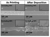
도 6의 (a) 및 (b)는 각각 본 발명의 실시예의 잉크로 제조된 패턴(Including HPC) 및 비교예의 잉크로 제조된 패턴(Excluding HPC), (c) 및 (d)는 도금을 거친 후의 패턴을 촬영한 평면 사진이다. 도 6의 (a) 내지 (d)의 사진에서 우측 작은 박스 안은 저배율의 전체 패턴을 보여주고 있다. 6 (a) and (b) are the patterns (Including HPC) prepared with the ink of the embodiment of the present invention and the pattern (Excluding HPC) prepared with the ink of the comparative example, (c) and (d) are after plating, respectively. This is a flat photo of the later pattern. In the photo of (a) to (d) of FIG. 6 , the small box on the right shows the entire pattern at low magnification.
먼저 도 6의 (a) 및 (c)에 도시된 바와 같이 HPC 첨가 잉크로 제조된 전구체 패턴에서는 균일한 선폭이 구현 가능하고, 도금 후에도 선폭 및 선폭의 균일성이 거의 유지됨을 알 수 있다. First, as shown in FIGS. 6(a) and 6(c), it can be seen that a uniform line width can be realized in the precursor pattern prepared with the HPC-added ink, and the line width and the uniformity of the line width are almost maintained even after plating.
그러나, 도 6의 (b) 및 (d)에 도시된 바와 같이, HPC 미첨가 잉크로 제조된 전구체 패턴은 선폭이 불균일하고, 도금 후에 지저분한 형태의 도금막이 형성된 것을 확인할 수 있다. 이것은 HPC가 첨가되지 않은 경우 60℃도 무전해도금 과정에서 패턴의 분해로 인해 발생한 결과이다. . However, as shown in (b) and (d) of FIG. 6 , it can be seen that the precursor pattern prepared with the non-HPC ink has non-uniform line width, and a messy plating film is formed after plating. This is a result of pattern decomposition during the electroless plating process at 60°C when no HPC is added. .
도 7의 (a) 내지 (d)는 본 발명의 실시예의 잉크로 제조된 패턴(Including HPC)의 도금 시간에 따라 형성된 도금막의 모폴로지를 보여주는 전자현미경 사진이다. 7 (a) to (d) are electron micrographs showing the morphology of the plating film formed according to the plating time of the pattern (Including HPC) prepared with the ink according to the embodiment of the present invention.
도 7로부터 도금 시간의 증가에 따라 입자 크기가 증가하며 도금막의 두께도 증가함을 알 수 있다. It can be seen from FIG. 7 that as the plating time increases, the particle size increases and the thickness of the plating film also increases.
도 8은 도금 시간(reaction time)에 따른 도금 패턴의 저항값을 측정한 결과를 나타낸 그래프이다. 8 is a graph showing the result of measuring the resistance value of the plating pattern according to the plating time (reaction time).
도 8을 참조하면, 도금 시간이 20분 이상인 경우 전기적 특성이 거의 일정하게 유지됨을 알 수 있다. 한편, 50분 도금한 경우, 도금막의 저항이 Bulk Cu의 비저항 대비 약 1.53배에 불과하여 높은 전도성을 갖는 도금막을 얻을 수 있음을 알 수 있다. Referring to FIG. 8 , it can be seen that when the plating time is 20 minutes or more, the electrical characteristics are maintained almost constant. On the other hand, in the case of plating for 50 minutes, it can be seen that the resistance of the plating film is only about 1.53 times that of bulk Cu, so that a plating film having high conductivity can be obtained.
< 실험예 4 : 접착력 평가><Experimental Example 4: Adhesion evaluation>
플라스틱 보드의 두 단자 사이에 실험예 3과 같이 20분 간 Cu 도금하여 도금 패턴을 형성하여 두 단자를 전기적으로 연결하였다. 도금 패턴 형성부에 점착 테이프를 붙인 후 점착 테이프를 제거하였을 때 도금 패턴의 벗겨짐 여부를 확인하였다. As in Experimental Example 3, Cu plating was performed between the two terminals of the plastic board for 20 minutes to form a plating pattern, and the two terminals were electrically connected. After attaching the adhesive tape to the plating pattern forming part, it was checked whether the plating pattern was peeled off when the adhesive tape was removed.
도 9는 점착 테이프 부착(attach) 후 및 제거 후(remove)를 촬영한 사진이다. 도시된 바와 같이, 점착 테이프 부착 전후에 단선은 없었음을 알 수 있다. 9 is a photograph taken after attaching and removing the adhesive tape. As shown, it can be seen that there was no disconnection before and after the adhesive tape was attached.
이상, 본 발명의 실시예를 통해 본 발명을 상술하였지만 이상의 설명은 본 발명을 예시한 것으로 본 발명이 이에 한정되는 것이 아니다. 첨부된 청구범위와 본 발명의 요지를 벗어남이 없이 당해 발명이 속하는 분야에서 통상의 지식을 가진 자라면 누구든지 다양한 변경 실시가 가능한 범위까지 본 발명의 범위에 속하는 것으로 간주 되어야 할 것이다. As mentioned above, although the present invention has been described above through the embodiments of the present invention, the above description is by way of illustration of the present invention, and the present invention is not limited thereto. Without departing from the scope of the appended claims and the scope of the present invention, it should be regarded as belonging to the scope of the present invention to the extent that various modifications can be made by any person skilled in the art to which the present invention pertains.
Claims (14)
촉매로서의 금속 이온;
상기 금속 이온과 상기 폴리머를 커플링하는 커플링제; 및
용매를 포함하고
상기 폴리머는 용매-폴리머 2원계의 온도-조성 상평형도 상에서 임계 온도 하한(Lower Critical Solution Temperature)을 가지고, 상기 임계 온도 하한은 30℃ 이상인 것을 특징으로 하는 도금용 촉매 잉크.polymer binder;
metal ions as catalysts;
a coupling agent coupling the metal ion and the polymer; and
contains a solvent
The polymer has a lower critical temperature limit (Lower Critical Solution Temperature) on the temperature-composition phase equilibrium of the solvent-polymer binary system, and the lower critical temperature limit is 30°C or higher.
상기 임계 온도 하한은 50℃ 이상인 것을 특징으로 하는 도금용 촉매 잉크.According to claim 1,
The lower limit of the critical temperature is a catalyst ink for plating, characterized in that 50 ℃ or more.
상기 용매는 물, 알코올, 또는 아세톤인 것을 특징으로 하는 도금용 촉매 잉크.According to claim 1,
The solvent is a catalyst ink for plating, characterized in that water, alcohol, or acetone.
상기 폴리머는 OH 작용기를 포함하는 것을 특징으로 하는 도금용 촉매 잉크.4. The method of claim 3,
The polymer is a catalyst ink for plating, characterized in that it comprises an OH functional group.
상기 폴리머는 Hydroxypropyl cellulose, Methyl cellulose, Hydroxypropylmethyle cellulose, Ethyl(hydroxyethyl)cellulose, Poly(N-isopropylacrylamide-co-acrylic acid) 및 Poly(propylene glycol)로 이루어진 그룹 중에서 선택된 최소한 1종을 포함하는 것을 특징으로 하는 도금용 촉매 잉크.4. The method of claim 3,
The polymer comprises at least one selected from the group consisting of Hydroxypropyl cellulose , Methyl cellulose , Hydroxypropylmethyle cellulose, Ethyl (hydroxyethyl) cellulose , Poly (N-isopropylacrylamide-co-acrylic acid) and Poly (propylene glycol) Catalyst ink for plating.
상기 금속 이온의 금속은 Ag, Fe, Co, Ni, Cu, Pd, Pt, Sn, Au로 이루어진 그룹 중에서 선택된 최소한 1종인 것을 특징으로 하는 도금용 촉매 잉크.According to claim 1,
The metal of the metal ion is at least one selected from the group consisting of Ag, Fe, Co, Ni, Cu, Pd, Pt, Sn, and Au.
상기 잉크는 점도가 5 mPa·s ~ 1,500 mPa·s인 것을 특징으로 하는 도금용 촉매 잉크.According to claim 1,
The ink has a viscosity of 5 mPa·s to 1,500 mPa·s.
상기 잉크는 손실 모듈러스가 저장 모듈러스보다 큰 것을 특징으로 하는 도금용 촉매 잉크.According to claim 1,
The ink is a catalyst ink for plating, characterized in that the loss modulus is greater than the storage modulus.
상기 전구체 패턴이 형성된 기재를 상기 용매-폴리머 2원계의 온도-조성 상평형도 상에서 임계 온도 하한(Lower Critical Solution Temperature) 이상의 온도로 유지되는 도금 용액 내에 침지하여 무전해 도금하여 도금 패턴을 형성하는 단계를 포함하고
상기 임계 온도 하한은 30℃ 이상인 것을 특징으로 하는 도금 방법.discharging a catalyst ink for plating comprising a polymer binder, a metal ion as a catalyst, a coupling agent for coupling the metal ion and the polymer, and a solvent to provide a substrate on which a precursor pattern is formed;
Forming a plating pattern by electroless plating by immersing the substrate on which the precursor pattern is formed in a plating solution maintained at a temperature above a lower critical solution temperature on the temperature-composition phase equilibrium of the solvent-polymer binary system. includes
The lower limit of the critical temperature is a plating method, characterized in that 30 ℃ or more.
상기 용매는 물이고,
상기 폴리머는 Hydroxypropyl cellulose, Methyl cellulose, Hydroxypropylmethyle cellulose, Ethyl(hydroxyethyl)cellulose, Poly(N-isopropylacrylamide-co-acrylic acid) 및 Poly(propylene glycol)로 이루어진 그룹 중에서 선택된 최소한 1종을 포함하는 것을 특징으로 하는 도금 방법.10. The method of claim 9,
the solvent is water,
The polymer comprises at least one selected from the group consisting of Hydroxypropyl cellulose , Methyl cellulose , Hydroxypropylmethyle cellulose, Ethyl (hydroxyethyl) cellulose , Poly (N-isopropylacrylamide-co-acrylic acid) and Poly (propylene glycol) plating method.
상기 임계 온도 하한은 50℃ 이상인 것을 특징으로 하는 도금 방법.10. The method of claim 9,
The lower limit of the critical temperature is a plating method, characterized in that 50 ℃ or more.
상기 기재 제공 단계에서 상기 도금용 촉매 잉크를 노즐을 통해 무가압 토출하는 것을 특징으로 하는 도금 방법.10. The method of claim 9,
A plating method, characterized in that in the step of providing the substrate, the catalyst ink for plating is discharged without pressure through a nozzle.
상기 도금용 촉매 잉크는 손실 모듈러스가 저장 모듈러스보다 큰 것을 특징으로 하는 도금 방법.
14. The method of claim 13,
The plating method, characterized in that the catalyst ink for plating has a loss modulus greater than a storage modulus.
Priority Applications (4)
| Application Number | Priority Date | Filing Date | Title |
|---|---|---|---|
| KR1020180114732A KR102458237B1 (en) | 2018-09-27 | 2018-09-27 | Catalyst Ink For Plating And Electroless Plating Pattern Forming Methods Using The Same |
| PCT/KR2018/012831 WO2020067601A1 (en) | 2018-09-27 | 2018-10-26 | Catalyst ink for plating and electroless plating method using same |
| US17/279,527 US20210340397A1 (en) | 2018-09-27 | 2018-10-26 | Catalyst ink for plating and electroless plating method using same |
| US18/770,498 US12545799B2 (en) | 2018-09-27 | 2024-07-11 | Catalyst ink for plating and electroless plating method using same |
Applications Claiming Priority (1)
| Application Number | Priority Date | Filing Date | Title |
|---|---|---|---|
| KR1020180114732A KR102458237B1 (en) | 2018-09-27 | 2018-09-27 | Catalyst Ink For Plating And Electroless Plating Pattern Forming Methods Using The Same |
Publications (2)
| Publication Number | Publication Date |
|---|---|
| KR20200035562A KR20200035562A (en) | 2020-04-06 |
| KR102458237B1 true KR102458237B1 (en) | 2022-10-25 |
Family
ID=69952990
Family Applications (1)
| Application Number | Title | Priority Date | Filing Date |
|---|---|---|---|
| KR1020180114732A Active KR102458237B1 (en) | 2018-09-27 | 2018-09-27 | Catalyst Ink For Plating And Electroless Plating Pattern Forming Methods Using The Same |
Country Status (3)
| Country | Link |
|---|---|
| US (2) | US20210340397A1 (en) |
| KR (1) | KR102458237B1 (en) |
| WO (1) | WO2020067601A1 (en) |
Families Citing this family (4)
| Publication number | Priority date | Publication date | Assignee | Title |
|---|---|---|---|---|
| KR102505053B1 (en) * | 2021-02-16 | 2023-03-03 | 주식회사 티엘비 | Ink composition for plating and manufacturing method of printed circuit board using same |
| KR102570845B1 (en) * | 2021-04-28 | 2023-08-29 | 주식회사 티엘비 | Ink composition for plating and manufacturing method of printed circuit board using same |
| KR102758411B1 (en) * | 2021-12-29 | 2025-01-23 | 주식회사 티엘비 | Ink composition for plating and manufacturing method of printed circuit board using same |
| KR102573184B1 (en) * | 2021-12-29 | 2023-09-01 | 주식회사 티엘비 | Ink composition for plating and manufacturing method of printed circuit board using same |
Citations (1)
| Publication number | Priority date | Publication date | Assignee | Title |
|---|---|---|---|---|
| JP2017210630A (en) | 2014-10-02 | 2017-11-30 | 日本板硝子株式会社 | Electroless plating substrate agent, production method thereof, and plated laminate using electroless plating substrate agent |
Family Cites Families (14)
| Publication number | Priority date | Publication date | Assignee | Title |
|---|---|---|---|---|
| US4912032A (en) * | 1986-04-17 | 1990-03-27 | Genetec Systems Corporation | Methods for selectively reacting ligands immobilized within a temperature-sensitive polymer gel |
| JP2004277688A (en) | 2003-01-23 | 2004-10-07 | Sumitomo Chem Co Ltd | Ink and electromagnetic wave shielding material |
| KR101325856B1 (en) * | 2005-09-30 | 2013-11-05 | 닛산 가가쿠 고교 가부시키 가이샤 | Chip provided with film having hole pattern with the use of thermoresponsive polymer and method of producing the same |
| KR101496501B1 (en) * | 2008-04-30 | 2015-02-26 | 아키레스 가부시키가이샤 | Plated molded article and method for producing the same |
| TWI433957B (en) * | 2008-09-23 | 2014-04-11 | Univ Nat Defense | Metallization method of substrate surface and through hole and catalyst used therein |
| KR101445461B1 (en) * | 2010-03-23 | 2014-09-26 | 제이엑스 닛코 닛세키 킨조쿠 가부시키가이샤 | Electroless plating pretreatment agent, electroless plating method using same, and electroless plated object |
| JP5734670B2 (en) * | 2011-01-07 | 2015-06-17 | 富士フイルム株式会社 | Composition for forming layer to be plated and method for producing laminate having metal film |
| KR101416579B1 (en) * | 2013-09-16 | 2014-07-09 | (주) 화인켐 | Conductive paste printed circuit board having plating layer and method for manufacturing the same |
| US20150240101A1 (en) * | 2014-02-24 | 2015-08-27 | Xerox Corporation | High silver content nanosilver ink for gravure and flexographic printing applications |
| WO2015187933A1 (en) * | 2014-06-04 | 2015-12-10 | 3D Systems, Incorporated | Inks comprising gellants for 3d printing |
| JP6072330B2 (en) * | 2015-04-01 | 2017-02-01 | 宮城県 | Electroless plating pretreatment ink composition for pattern plating and formation method of electroless plating film |
| WO2016208886A1 (en) * | 2015-06-22 | 2016-12-29 | 한국전기연구원 | Metal/two-dimensional nanomaterial hybrid conductive film and method for manufacturing same |
| WO2017127708A1 (en) * | 2016-01-22 | 2017-07-27 | Voxel8, Inc. | 3d printable composite waterborne dispersions |
| CN107365529A (en) * | 2017-07-31 | 2017-11-21 | 珠海纳金科技有限公司 | A kind of electrically conductive ink and preparation method and volume to volume conductive film and preparation method |
-
2018
- 2018-09-27 KR KR1020180114732A patent/KR102458237B1/en active Active
- 2018-10-26 WO PCT/KR2018/012831 patent/WO2020067601A1/en not_active Ceased
- 2018-10-26 US US17/279,527 patent/US20210340397A1/en not_active Abandoned
-
2024
- 2024-07-11 US US18/770,498 patent/US12545799B2/en active Active
Patent Citations (1)
| Publication number | Priority date | Publication date | Assignee | Title |
|---|---|---|---|---|
| JP2017210630A (en) | 2014-10-02 | 2017-11-30 | 日本板硝子株式会社 | Electroless plating substrate agent, production method thereof, and plated laminate using electroless plating substrate agent |
Also Published As
| Publication number | Publication date |
|---|---|
| US20210340397A1 (en) | 2021-11-04 |
| KR20200035562A (en) | 2020-04-06 |
| US20240360331A1 (en) | 2024-10-31 |
| US12545799B2 (en) | 2026-02-10 |
| WO2020067601A1 (en) | 2020-04-02 |
Similar Documents
| Publication | Publication Date | Title |
|---|---|---|
| US12545799B2 (en) | Catalyst ink for plating and electroless plating method using same | |
| JP5982033B2 (en) | Metal fine particle dispersion, copper fine particle dispersion, method for producing copper fine particle dispersion, and method for producing conductive substrate | |
| JP4128885B2 (en) | Method for forming fine wiring pattern | |
| DE102007037079A1 (en) | Silver-containing aqueous formulation and its use for the production of electrically conductive or reflective coatings | |
| KR102458238B1 (en) | Catalyst Ink For 3D structure, And Manufacturing Methods of 3D Structure Using The Same | |
| US10307825B2 (en) | Metal powder, ink, sintered body, substrate for printed circuit board, and method for manufacturing metal powder | |
| WO2016117575A1 (en) | Substrate for printed wiring board, printed wiring board, and method for manufacturing printed wiring board | |
| US10076032B2 (en) | Substrate for printed circuit board, printed circuit board, and method for producing substrate for printed circuit board | |
| KR101520412B1 (en) | Flexible printed circuit board by laser processing and printing process, and method for manufacturing the same | |
| KR20220116955A (en) | Ink composition for plating and manufacturing method of printed circuit board using same | |
| JP6466110B2 (en) | Printed wiring board substrate, printed wiring board, and printed wiring board manufacturing method | |
| KR101416579B1 (en) | Conductive paste printed circuit board having plating layer and method for manufacturing the same | |
| JP5087384B2 (en) | Manufacturing method of conductive member and conductive member | |
| EP3406757A1 (en) | A process for preparing a copper coated conductive carbon-based substrate | |
| WO2019077816A1 (en) | Base material for printed wiring board, and printed wiring board | |
| JPH07245467A (en) | Manufacture of printed wiring board | |
| KR100856100B1 (en) | Substrate surface treatment method and wiring pattern formation method using the same | |
| CN101457048B (en) | Conductive pattern forming ink, conductive pattern, and wiring substrate | |
| CN107113970B (en) | Substrate for printed circuit board, printed circuit board and method for producing substrate for printed circuit board | |
| JP2010232639A (en) | Method of forming metallic pattern, and metallic pattern | |
| CN101457043A (en) | Conductive pattern forming ink, conductive pattern, and wiring substrate | |
| KR20240092647A (en) | Ink composition for plating and manufacturing method of printed circuit board using same | |
| KR20140049632A (en) | Conductive paste printed circuit board having plating layer and method for manufacturing the same | |
| KR20240030220A (en) | Ink composition for plating and manufacturing method of printed circuit board using same | |
| KR102891953B1 (en) | Ink composition for plating and manufacturing method of printed circuit board using the same |
Legal Events
| Date | Code | Title | Description |
|---|---|---|---|
| PA0109 | Patent application |
Patent event code: PA01091R01D Comment text: Patent Application Patent event date: 20180927 |
|
| PG1501 | Laying open of application | ||
| A201 | Request for examination | ||
| PA0201 | Request for examination |
Patent event code: PA02012R01D Patent event date: 20200522 Comment text: Request for Examination of Application Patent event code: PA02011R01I Patent event date: 20180927 Comment text: Patent Application |
|
| E902 | Notification of reason for refusal | ||
| PE0902 | Notice of grounds for rejection |
Comment text: Notification of reason for refusal Patent event date: 20220330 Patent event code: PE09021S01D |
|
| E701 | Decision to grant or registration of patent right | ||
| PE0701 | Decision of registration |
Patent event code: PE07011S01D Comment text: Decision to Grant Registration Patent event date: 20221011 |
|
| GRNT | Written decision to grant | ||
| PR0701 | Registration of establishment |
Comment text: Registration of Establishment Patent event date: 20221019 Patent event code: PR07011E01D |
|
| PR1002 | Payment of registration fee |
Payment date: 20221020 End annual number: 3 Start annual number: 1 |
|
| PG1601 | Publication of registration |