KR102457198B1 - Electronic device including diplexer adjusting cutoff frequency regarding adjustment of receiving frequency band - Google Patents
Electronic device including diplexer adjusting cutoff frequency regarding adjustment of receiving frequency band Download PDFInfo
- Publication number
- KR102457198B1 KR102457198B1 KR1020180044192A KR20180044192A KR102457198B1 KR 102457198 B1 KR102457198 B1 KR 102457198B1 KR 1020180044192 A KR1020180044192 A KR 1020180044192A KR 20180044192 A KR20180044192 A KR 20180044192A KR 102457198 B1 KR102457198 B1 KR 102457198B1
- Authority
- KR
- South Korea
- Prior art keywords
- frequency band
- reception
- duplexer
- filter
- electronic device
- Prior art date
- Legal status (The legal status is an assumption and is not a legal conclusion. Google has not performed a legal analysis and makes no representation as to the accuracy of the status listed.)
- Active
Links
Images


Classifications
-
- H—ELECTRICITY
- H04—ELECTRIC COMMUNICATION TECHNIQUE
- H04L—TRANSMISSION OF DIGITAL INFORMATION, e.g. TELEGRAPHIC COMMUNICATION
- H04L5/00—Arrangements affording multiple use of the transmission path
- H04L5/14—Two-way operation using the same type of signal, i.e. duplex
-
- H—ELECTRICITY
- H04—ELECTRIC COMMUNICATION TECHNIQUE
- H04B—TRANSMISSION
- H04B1/00—Details of transmission systems, not covered by a single one of groups H04B3/00 - H04B13/00; Details of transmission systems not characterised by the medium used for transmission
- H04B1/005—Details of transmission systems, not covered by a single one of groups H04B3/00 - H04B13/00; Details of transmission systems not characterised by the medium used for transmission adapting radio receivers, transmitters andtransceivers for operation on two or more bands, i.e. frequency ranges
- H04B1/0053—Details of transmission systems, not covered by a single one of groups H04B3/00 - H04B13/00; Details of transmission systems not characterised by the medium used for transmission adapting radio receivers, transmitters andtransceivers for operation on two or more bands, i.e. frequency ranges with common antenna for more than one band
- H04B1/0057—Details of transmission systems, not covered by a single one of groups H04B3/00 - H04B13/00; Details of transmission systems not characterised by the medium used for transmission adapting radio receivers, transmitters andtransceivers for operation on two or more bands, i.e. frequency ranges with common antenna for more than one band using diplexing or multiplexing filters for selecting the desired band
-
- H—ELECTRICITY
- H04—ELECTRIC COMMUNICATION TECHNIQUE
- H04B—TRANSMISSION
- H04B1/00—Details of transmission systems, not covered by a single one of groups H04B3/00 - H04B13/00; Details of transmission systems not characterised by the medium used for transmission
- H04B1/02—Transmitters
- H04B1/04—Circuits
- H04B1/0458—Arrangements for matching and coupling between power amplifier and antenna or between amplifying stages
-
- H—ELECTRICITY
- H04—ELECTRIC COMMUNICATION TECHNIQUE
- H04B—TRANSMISSION
- H04B1/00—Details of transmission systems, not covered by a single one of groups H04B3/00 - H04B13/00; Details of transmission systems not characterised by the medium used for transmission
- H04B1/06—Receivers
- H04B1/16—Circuits
- H04B1/18—Input circuits, e.g. for coupling to an antenna or a transmission line
-
- H—ELECTRICITY
- H04—ELECTRIC COMMUNICATION TECHNIQUE
- H04B—TRANSMISSION
- H04B1/00—Details of transmission systems, not covered by a single one of groups H04B3/00 - H04B13/00; Details of transmission systems not characterised by the medium used for transmission
- H04B1/38—Transceivers, i.e. devices in which transmitter and receiver form a structural unit and in which at least one part is used for functions of transmitting and receiving
- H04B1/40—Circuits
- H04B1/44—Transmit/receive switching
- H04B1/48—Transmit/receive switching in circuits for connecting transmitter and receiver to a common transmission path, e.g. by energy of transmitter
-
- H—ELECTRICITY
- H04—ELECTRIC COMMUNICATION TECHNIQUE
- H04B—TRANSMISSION
- H04B1/00—Details of transmission systems, not covered by a single one of groups H04B3/00 - H04B13/00; Details of transmission systems not characterised by the medium used for transmission
- H04B1/38—Transceivers, i.e. devices in which transmitter and receiver form a structural unit and in which at least one part is used for functions of transmitting and receiving
- H04B1/40—Circuits
- H04B1/50—Circuits using different frequencies for the two directions of communication
- H04B1/52—Hybrid arrangements, i.e. arrangements for transition from single-path two-direction transmission to single-direction transmission on each of two paths or vice versa
Landscapes
- Engineering & Computer Science (AREA)
- Signal Processing (AREA)
- Computer Networks & Wireless Communication (AREA)
- Transceivers (AREA)
Abstract
무선으로 제1 주파수 대역 및 제2 주파수 대역의 신호를 송신 또는 수신하는 하나 이상의 안테나들을 포함하는 안테나 모듈; 상기 제1 주파수 대역을 제1 송신 주파수 대역 및 제1 수신 주파수 대역으로 분리하고, 상기 제1 수신 주파수 대역을 조정할 수 있는 제1 듀플렉서; 상기 제2 주파수 대역을 제2 송신 주파수 대역 및 제2 수신 주파수 대역으로 분리하고, 상기 제2 수신 주파수 대역을 조정할 수 있는 제2 듀플렉서; 및 상기 안테나 모듈과 전기적으로 연결된 제1 단자, 상기 제1 주파수 대역을 통과시킬 수 있는 제1 필터, 상기 제1 필터 및 상기 제1 듀플렉서와 전기적으로 연결된 제2 단자, 상기 제2 주파수 대역을 통과시킬 수 있는 제2 필터, 및 상기 제2 필터 및 상기 제2 듀플렉서와 전기적으로 연결된 제3 단자를 포함하는 다이플렉서를 포함하고, 상기 다이플렉서는 상기 제1 듀플렉서를 통해 조정된 상기 제1 수신 주파수 대역 또는 상기 제2 듀플렉서를 통해 조정된 상기 제2 수신 주파수 대역과 관련하여 상기 제1 필터 또는 상기 제2 필터의 컷오프 주파수를 조정할 수 있는 전자 장치가 개시된다. 이 외에도 명세서를 통해 파악되는 다양한 실시 예가 가능하다.an antenna module including one or more antennas for wirelessly transmitting or receiving signals of a first frequency band and a second frequency band; a first duplexer capable of dividing the first frequency band into a first transmission frequency band and a first reception frequency band, and adjusting the first reception frequency band; a second duplexer that divides the second frequency band into a second transmit frequency band and a second receive frequency band and adjusts the second receive frequency band; and a first terminal electrically connected to the antenna module, a first filter capable of passing the first frequency band, a second terminal electrically connected to the first filter and the first duplexer, and passing the second frequency band and a diplexer including a second filter capable of activating a second filter, and a third terminal electrically connected to the second filter and the second duplexer, wherein the diplexer is adjusted through the first duplexer. Disclosed is an electronic device capable of adjusting a cutoff frequency of the first filter or the second filter in relation to a reception frequency band or the second reception frequency band adjusted through the second duplexer. In addition to this, various embodiments identified through the specification are possible.
Description
본 문서에서 개시되는 실시 예들은 컷오프 주파수를 조정하여 하나 이상의 수신 주파수 대역을 조정하여 무선 통신을 수행하는 기술과 관련된다.Embodiments disclosed in this document relate to a technique for performing wireless communication by adjusting one or more reception frequency bands by adjusting a cutoff frequency.
무선 통신을 수행하는 전자 장치는 안테나를 통해 무선으로 하나 이상의 주파수 대역의 RF(radio frequency) 신호를 수신한다. 전자 장치가 동일한 시간 동안 보다 많은 양의 정보를 수신하기 위해, 무선 통신을 수행하는 전자 장치의 수신 속도를 증가시키는 것이 필요하다. 전자 장치의 수신 속도를 증가시키기 위해, 전자 장치는 복수의 주파수 대역들(bands)을 이용하여 RF 신호들을 수신한다. 전자 장치가 복수의 주파수 대역들을 이용함에 따라, 전자 장치에서 RF 신호들을 수신하는 속도를 증가시킬 수 있다. 전자 장치는 복수의 주파수 대역들을 이용하여 수신한 RF 신호인 복수의 수신 신호들을 RF 집적 회로(integrated circuit, IC)에서 획득한다.An electronic device performing wireless communication wirelessly receives radio frequency (RF) signals of one or more frequency bands through an antenna. In order for the electronic device to receive a greater amount of information during the same time, it is necessary to increase the reception speed of the electronic device performing wireless communication. In order to increase the reception speed of the electronic device, the electronic device receives RF signals using a plurality of frequency bands. As the electronic device uses a plurality of frequency bands, the speed at which the electronic device receives RF signals may be increased. The electronic device acquires a plurality of received signals that are RF signals received using a plurality of frequency bands from an RF integrated circuit (IC).
전자 장치는 복수의 주파수 대역들을 수신 주파수 대역으로 사용하여 수신 신호들을 수신하는 반송파 집성(carrier aggregation, CA) 모드를 구현한다. 전자 장치는 반송파 집성 모드를 통해 복수의 주파수 대역들을 묶어서 사용함으로써 무선 통신의 수신 속도를 증가시킬 수 있다.The electronic device implements a carrier aggregation (CA) mode in which reception signals are received by using a plurality of frequency bands as reception frequency bands. The electronic device may increase the reception speed of wireless communication by grouping and using a plurality of frequency bands through the carrier aggregation mode.
무선 통신을 수행하는 전자 장치가 복수의 주파수 대역을 이용함에 따라, 전자 장치에서 사용하는 주파수 대역의 개수가 증가하였다. 전자 장치가 사용하는 주파수 대역의 개수가 증가함에 따라, 전자 장치는 미리 설정되어 있는 복수의 주파수 대역들 중 로우-로우(low-low), 미드-미드(mid-mid), 또는 하이-하이(high-high)의 주파수 대역들을 선택하여 사용할 수 있다. 로우-로우, 미드-미드, 또는 하이-하이의 수신 주파수 대역들은 적어도 일부가 서로 중첩될 수 있다. 복수의 수신 주파수 대역들의 적어도 일부가 서로 중첩된 경우, 전자 장치에서 반송파 집성 모드를 구현하는 것이 용이하지 않다.As electronic devices performing wireless communication use a plurality of frequency bands, the number of frequency bands used by electronic devices has increased. As the number of frequency bands used by the electronic device increases, the electronic device uses a low-low, mid-mid, or high-high frequency band among a plurality of preset frequency bands. high-high) frequency bands can be selected and used. The low-low, mid-mid, or high-high reception frequency bands may at least partially overlap each other. When at least some of the plurality of reception frequency bands overlap each other, it is not easy to implement the carrier aggregation mode in the electronic device.
본 문서에 개시되는 일 실시 예에 따른 전자 장치는, 무선으로 제1 주파수 대역 및 제2 주파수 대역의 신호를 송신 또는 수신하는 하나 이상의 안테나들을 포함하는 안테나 모듈; 상기 제1 주파수 대역을 제1 송신 주파수 대역 및 제1 수신 주파수 대역으로 분리하고, 상기 제1 수신 주파수 대역을 조정할 수 있는 제1 듀플렉서; 상기 제2 주파수 대역을 제2 송신 주파수 대역 및 제2 수신 주파수 대역으로 분리하고, 상기 제2 수신 주파수 대역을 조정할 수 있는 제2 듀플렉서; 및 상기 안테나 모듈과 전기적으로 연결된 제1 단자, 상기 제1 주파수 대역을 통과시킬 수 있는 제1 필터, 상기 제1 필터 및 상기 제1 듀플렉서와 전기적으로 연결된 제2 단자, 상기 제2 주파수 대역을 통과시킬 수 있는 제2 필터, 및 상기 제2 필터 및 상기 제2 듀플렉서와 전기적으로 연결된 제3 단자를 포함하는 다이플렉서를 포함하고, 상기 다이플렉서는 상기 제1 듀플렉서를 통해 조정된 상기 제1 수신 주파수 대역 또는 상기 제2 듀플렉서를 통해 조정된 상기 제2 수신 주파수 대역과 관련하여 상기 제1 필터 또는 상기 제2 필터의 컷오프 주파수를 조정할 수 있다.An electronic device according to an embodiment disclosed in this document includes: an antenna module including one or more antennas for wirelessly transmitting or receiving signals of a first frequency band and a second frequency band; a first duplexer capable of dividing the first frequency band into a first transmission frequency band and a first reception frequency band, and adjusting the first reception frequency band; a second duplexer that divides the second frequency band into a second transmit frequency band and a second receive frequency band and adjusts the second receive frequency band; and a first terminal electrically connected to the antenna module, a first filter capable of passing the first frequency band, a second terminal electrically connected to the first filter and the first duplexer, and passing the second frequency band and a diplexer including a second filter capable of activating a second filter, and a third terminal electrically connected to the second filter and the second duplexer, wherein the diplexer is adjusted through the first duplexer. A cutoff frequency of the first filter or the second filter may be adjusted in relation to a reception frequency band or the second reception frequency band adjusted through the second duplexer.
또한, 본 문서에 개시되는 일 실시 예에 따른 전자 장치는, 무선으로 제1 주파수 대역 및 제2 주파수 대역의 신호를 송신 또는 수신하는 하나 이상의 안테나들; 상기 제1 주파수 대역을 제1 송신 주파수 대역 및 제1 수신 주파수 대역으로 분리하고, 상기 제1 수신 주파수 대역을 조정할 수 있는 제1 듀플렉서; 상기 제2 주파수 대역을 제2 송신 주파수 대역 및 제2 수신 주파수 대역으로 분리하고, 상기 제2 수신 주파수 대역을 조정할 수 있는 제2 듀플렉서; 및 상기 하나 이상의 안테나들을 포함하는 안테나 모듈과 전기적으로 연결된 제1 단자, 상기 제1 주파수 대역을 통과시킬 수 있는 제1 필터, 상기 제1 필터 및 상기 제1 듀플렉서와 전기적으로 연결된 제2 단자, 상기 제2 주파수 대역을 통과시킬 수 있는 제2 필터, 및 상기 제2 필터 및 상기 제2 듀플렉서와 전기적으로 연결된 제3 단자를 포함하고, 상기 제1 수신 주파수 대역 및 상기 제2 수신 주파수 대역의 사용 여부에 따라 상기 제1 필터 또는 상기 제2 필터의 컷 오프 주파수를 조정할 수 있는 다이플렉서; 및 상기 제1 듀플렉서, 상기 제2 듀플렉서, 및 상기 다이플렉서와 작동적으로 연결된(operationally connected) 프로세서를 포함하고, 상기 프로세서는, 제1 모드인 경우 상기 컷 오프 주파수를 상기 제1 수신 주파수 대역보다 높게 조정(adjust)하고, 제2 모드인 경우 상기 컷 오프 주파수를 상기 제1 수신 주파수 대역보다 낮게 조정하고, 상기 제2 듀플렉서를 통해 상기 제2 수신 주파수 대역을 상기 조정된 컷 오프 주파수보다 낮은 주파수 대역으로 조정하고, 및 제3 모드인 경우 상기 컷 오프 주파수를 상기 제2 수신 주파수 대역보다 높게 조정하고, 상기 제1 듀플렉서를 통해 상기 제1 수신 주파수 대역을 상기 조정된 컷 오프 주파수보다 높은 주파수 대역으로 조정한다.In addition, an electronic device according to an embodiment of the present disclosure may include one or more antennas for wirelessly transmitting or receiving signals of a first frequency band and a second frequency band; a first duplexer capable of dividing the first frequency band into a first transmission frequency band and a first reception frequency band, and adjusting the first reception frequency band; a second duplexer that divides the second frequency band into a second transmit frequency band and a second receive frequency band and adjusts the second receive frequency band; and a first terminal electrically connected to an antenna module including the one or more antennas, a first filter capable of passing the first frequency band, a second terminal electrically connected to the first filter and the first duplexer, the a second filter capable of passing a second frequency band, and a third terminal electrically connected to the second filter and the second duplexer, whether the first reception frequency band and the second reception frequency band are used a diplexer capable of adjusting a cut-off frequency of the first filter or the second filter according to the ? and a processor operatively connected to the first duplexer, the second duplexer, and the diplexer, wherein the processor adjusts the cut-off frequency to the first reception frequency band in a first mode. adjust higher, adjust the cut-off frequency lower than the first reception frequency band in the second mode, and adjust the second reception frequency band through the second duplexer to be lower than the adjusted cut-off frequency adjusting to a frequency band, and adjusting the cut-off frequency to be higher than the second receiving frequency band in the third mode, and adjusting the first receiving frequency band through the first duplexer to a frequency higher than the adjusted cut-off frequency adjust to the band.
또한, 본 문서에 개시되는 일 실시 예에 따른 전자 장치는, 제1 주파수 대역 및 상기 제1 주파수 대역과 적어도 일부가 중첩된 제2 주파수 대역을 이용한 무선 통신을 지원하는 통신 회로; 및 상기 통신 회로와 전기적으로 연결되는 하나 이상의 안테나들을 포함하고, 상기 통신 회로는, 상기 하나 이상의 안테나들과 연결되고, 상기 제1 주파수 대역을 통해 획득한 제1 수신 신호와 상기 제2 주파수 대역을 통해 획득한 제2 수신 신호 중 적어도 하나를 컷 오프 주파수를 이용하여 선택적으로 통과시키는 다이플렉서를 포함하고, 상기 통신 회로는 상기 제1 주파수 대역 및 상기 제2 주파수 대역 중 적어도 하나의 주파수 대역의 사용 여부에 따라 상기 다이플렉서의 컷 오프 주파수를 조절하도록 설정된다.In addition, an electronic device according to an embodiment of the present disclosure may include: a communication circuit supporting wireless communication using a first frequency band and a second frequency band at least partially overlapping the first frequency band; and one or more antennas electrically connected to the communication circuit, wherein the communication circuit is connected to the one or more antennas and transmits a first received signal obtained through the first frequency band and the second frequency band. and a diplexer for selectively passing at least one of the second received signals obtained through the cut-off frequency, wherein the communication circuit comprises at least one of the first frequency band and the second frequency band. It is set to adjust the cut-off frequency of the diplexer according to whether or not it is used.
본 문서에 개시되는 실시 예들에 따르면, 전자 장치는 적어도 일부가 중첩된 복수의 주파수 대역들을 사용하는 경우 수신 주파수 대역들의 사용 여부에 따라 컷 오프 주파수를 조정할 수 있다. 전자 장치는 수신 주파수 대역들을 모두 사용하는 경우에도 수신 신호를 모두 수신할 수 있다. 이에 따라, 전자 장치는 복수의 수신 주파수 대역들의 적어도 일부가 서로 중첩된 경우에도 반송파 집성 모드를 구현함으로써 수신 신호를 수신하는 속도를 향상시킬 수 있다. 즉, 전자 장치가 복수의 주파수 대역들 중 로우-로우, 미드-미드, 또는 하이-하이의 주파수 대역들을 선택하여 사용하는 경우에도 반송파 집성을 구현할 수 있어, 복수의 주파수 대역들을 보다 자유롭게 설정할 수 있다.According to embodiments disclosed in this document, when using a plurality of frequency bands at least partially overlapping, the electronic device may adjust the cut-off frequency according to whether reception frequency bands are used. The electronic device may receive all of the reception signals even when all reception frequency bands are used. Accordingly, even when at least some of the plurality of reception frequency bands overlap each other, the electronic device may improve the reception speed of the reception signal by implementing the carrier aggregation mode. That is, even when the electronic device selects and uses low-low, mid-mid, or high-high frequency bands from among the plurality of frequency bands, carrier aggregation can be implemented, so that the plurality of frequency bands can be set more freely. .
이 외에, 본 문서를 통해 직접적 또는 간접적으로 파악되는 다양한 효과들이 제공될 수 있다.In addition, various effects directly or indirectly identified through this document may be provided.
도 1은 일 실시 예에 따른 전자 장치를 나타낸 도면이다.
도 2는 일 실시 예에 따른 전자 장치가 사용하는 복수의 주파수 대역들을 나타낸 도면이다.
도 3은 일 실시 예에 따른 전자 장치가 제1 주파수 대역을 사용하는 경우의 도면이다.
도 4는 일 실시 예에 따른 전자 장치가 제1 주파수 대역을 사용하는 경우의 복수의 주파수 대역들 및 컷 오프 주파수를 나타낸 도면이다.
도 5는 일 실시 예에 따른 전자 장치가 제2 주파수 대역을 사용하는 경우의 도면이다.
도 6은 일 실시 예에 따른 전자 장치가 제2 주파수 대역을 사용하는 경우의 복수의 주파수 대역들 및 컷 오프 주파수를 나타낸 도면이다.
도 7은 일 실시 예에 따른 전자 장치가 제1 주파수 대역과 제2 주파수 대역을 사용하여 반송파 집성 모드로 동작하는 경우의 도면이다.
도 8은 일 실시 예에 따른 전자 장치가 제1 주파수 대역과 제2 주파수 대역을 사용하여 반송파 집성 모드로 동작하는 경우의 복수의 주파수 대역들 및 컷 오프 주파수를 나타낸 도면이다.
도 9는 일 실시 예에 따른 전자 장치를 나타낸 블록도이다.
도 10은 일 실시 예에 따른 전자 장치의 제어 방법을 나타낸 흐름도이다.
도 11은 다른 실시 예에 따른 전자 장치를 나타낸 도면이다.
도 12는 다른 실시 예에 따른 전자 장치가 제1 주파수 대역을 사용하는 경우의 도면이다.
도 13은 다른 실시 예에 따른 전자 장치가 제2 주파수 대역을 사용하는 경우의 도면이다.
도 14는 다른 실시 예에 따른 전자 장치가 제1 주파수 대역과 제2 주파수 대역을 사용하여 반송파 집성 모드로 동작하는 경우의 도면이다.
도 15는 다양한 실시 예에 따른 네트워크 환경 내의 전자 장치를 나타낸다.
도면의 설명과 관련하여, 동일 또는 유사한 구성요소에 대해서는 동일 또는 유사한 참조 부호가 사용될 수 있다.1 is a diagram illustrating an electronic device according to an embodiment.
2 is a diagram illustrating a plurality of frequency bands used by an electronic device according to an embodiment.
3 is a diagram illustrating a case in which an electronic device uses a first frequency band according to an embodiment.
4 is a diagram illustrating a plurality of frequency bands and cut-off frequencies when an electronic device uses a first frequency band according to an embodiment.
5 is a diagram illustrating a case in which an electronic device uses a second frequency band according to an exemplary embodiment.
6 is a diagram illustrating a plurality of frequency bands and cut-off frequencies when an electronic device uses a second frequency band according to an embodiment.
7 is a diagram illustrating a case in which an electronic device operates in a carrier aggregation mode using a first frequency band and a second frequency band according to an embodiment.
8 is a diagram illustrating a plurality of frequency bands and cut-off frequencies when an electronic device operates in a carrier aggregation mode using a first frequency band and a second frequency band, according to an embodiment.
9 is a block diagram illustrating an electronic device according to an embodiment.
10 is a flowchart illustrating a method of controlling an electronic device according to an exemplary embodiment.
11 is a diagram illustrating an electronic device according to another exemplary embodiment.
12 is a diagram illustrating a case in which an electronic device uses a first frequency band according to another exemplary embodiment.
13 is a diagram illustrating a case in which an electronic device uses a second frequency band according to another embodiment.
14 is a diagram illustrating a case in which an electronic device operates in a carrier aggregation mode using a first frequency band and a second frequency band according to another embodiment.
15 illustrates an electronic device in a network environment according to various embodiments of the present disclosure.
In connection with the description of the drawings, the same or similar reference numerals may be used for the same or similar components.
이하, 본 발명의 다양한 실시 예가 첨부된 도면을 참조하여 기재된다. 그러나, 이는 본 발명을 특정한 실시 형태에 대해 한정하려는 것이 아니며, 본 발명의 실시 예의 다양한 변경(modification), 균등물(equivalent), 및/또는 대체물(alternative)을 포함하는 것으로 이해되어야 한다. Hereinafter, various embodiments of the present invention will be described with reference to the accompanying drawings. However, this is not intended to limit the present invention to specific embodiments, and it should be understood that various modifications, equivalents, and/or alternatives of the embodiments of the present invention are included.
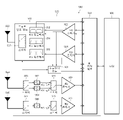
도 1은 일 실시 예에 따른 전자 장치(100)를 나타낸 도면이다. 일 실시 예에 따른 전자 장치(100)는 하나 이상의 안테나들(110)(antennas), 제1 듀플렉서(120), 제2 듀플렉서(130), 및 다이플렉서(140)를 포함할 수 있다.1 is a diagram illustrating an
일 실시 예에 따른 하나 이상의 안테나들(110)은 미리 설정된 복수의 주파수 대역들의 신호를 무선으로 수신할 수 있다. 하나 이상의 안테나들(110)은 안테나 배열(antenna array) 또는 안테나 모듈(antenna module)을 구성할 수 있다. 하나 이상의 안테나들(110)을 이루는 안테나 각각은 하나의 주파수 대역에 포함된 신호들을 수신할 수 있다. 예를 들어, 하나 이상의 안테나들(110)은 무선으로 제1 주파수 대역의 신호를 수신하는 제1 안테나 및 무선으로 제2 주파수 대역의 신호를 수신하는 제2 안테나를 포함할 수 있다. 그러나 이에 한정되지 않으며, 하나 이상의 안테나들(110)을 이루는 안테나 각각은 인접한 복수의 대역 주파수들에 포함된 신호들을 수신할 수 있다. 또한, 하나 이상의 안테나들(110)을 이루는 안테나 각각은 하나의 대역 주파수에 포함된 복수의 채널들 중 일부 채널들에 포함된 신호들을 수신할 수 있다.The one or
일 실시 예에 따른 제1 주파수 대역은 제1 수신 주파수 대역 및 제1 송신 주파수 대역을 포함할 수 있다. 제1 수신 주파수 대역은 제1 송신 주파수 대역으로부터 소정의 주파수 범위만큼 서로 이격될 수 있다. 본 문서에서는 제1 수신 주파수 대역의 주파수 범위가 제1 송신 주파수 대역의 주파수 범위보다 낮은 경우를 가정하여 서술하였다. 그러나 이에 한정되지 않으며, 제1 수신 주파수 대역의 주파수 범위가 제1 송신 주파수 대역의 주파수 범위보다 높을 수 있다.The first frequency band according to an embodiment may include a first reception frequency band and a first transmission frequency band. The first reception frequency band may be spaced apart from each other by a predetermined frequency range from the first transmission frequency band. In this document, it is assumed that the frequency range of the first reception frequency band is lower than the frequency range of the first transmission frequency band. However, the present invention is not limited thereto, and the frequency range of the first reception frequency band may be higher than the frequency range of the first transmission frequency band.
일 실시 예에 따른 제1 듀플렉서(120)는 제1 주파수 대역의 신호를 제1 수신 신호와 제1 송신 신호로 분리할 수 있다. 제1 수신 신호는 제1 수신 주파수 대역에 해당하는 신호이고, 제1 송신 신호는 제1 송신 주파수 대역에 해당하는 신호이다. 제1 듀플렉서(120)는 필터 회로(121)(filter circuit) 및 매칭 회로(123)(matching circuit)를 포함할 수 있다.The
일 실시 예에서, 필터 회로(121)는 지정된 공진 주파수 대역을 갖는 하나 이상의 대역 통과 필터(band pass filter, BPF)를 포함할 수 있다. 필터 회로(121)는 제1 송신 주파수 대역을 통과시키는 대역 통과 필터와 제1 수신 주파수 대역을 통과시키는 대역 통과 필터의 결합을 통해 구현될 수 있다. 필터 회로(121)는 제1 주파수 대역 이외의 신호를 필터링(filtering) 할 수 있다.In an embodiment, the
일 실시 예에서, 매칭 회로(123)는 하나 이상의 안테나들(110)과 필터 회로(121)의 임피던스(impedance)를 매칭시킬 수 있다. 매칭 회로(123)는 필터 회로(121)를 구성하는 대역 통과 필터의 통과 대역을 가변시킬 수 있다. 매칭 회로(123)를 포함하는 제1 듀플렉서(120)는 사용하는 제1 수신 주파수 대역을 조정할 수 있는(tunable) 듀플렉서일 수 있다. 매칭 회로(123)는 사용하는 제1 수신 주파수 대역의 최고값 또는 최저값을 변화시킬 수 있다. 매칭 회로(123)는 사용하는 제1 수신 주파수 대역의 폭을 변화시킬 수 있다.In an embodiment, the
일 실시 예에서, 매칭 회로(123)는 복수 개의 인덕터들, 복수 개의 캐패시터들, 및 복수 개의 스위치들을 포함할 수 있다. 스위치는 인덕터와 캐패시터 사이에 배치될 수 있다. 스위치가 개방(open)되는 경우, 스위치와 연결된 인덕터와 캐패시터는 전기적으로 차단될 수 있다. 스위치가 단락(short)되는 경우, 스위치와 연결된 인덕터와 캐패시터는 전기적으로 연결될 수 있다. 매칭 회로(123)는 스위치를 작동시키기 위해 전원 공급부(예: 도 15의 전력 관리 모듈(1588))로부터 전압(예: VDD 전압)을 공급받을 수 있다. 매칭 회로(123)는 스위치의 개방 및 단락을 제어할 수 있는 제어 신호를 공급받을 수 있다.In an embodiment, the
일 실시 예에서, 매칭 회로(123)는 매칭을 가변할 수 있다. 매칭 회로(123)는 매칭되는 쪽을 기준으로 임피던스(impedance)를 가변시킬 수 있다. 매칭 회로(123)는 임피던스를 가변시키기 위해 복수 개의 스위치들과 연결된 복수 개의 인덕터들 및 복수 개의 캐패시터들의 개수를 가변시킬 수 있다. 매칭 회로(123)는 매칭되는 소자와 동일한 임피던스 값을 갖도록 매칭을 가변할 수 있다. 예를 들어, 제1 듀플렉서(120)의 매칭 회로(123)는 다이플렉서(140)의 매칭 회로와 동일한 임피던스 값을 갖도록 매칭될 수 있다.In an embodiment, the
일 실시 예에 따른 제2 주파수 대역은 제2 수신 주파수 대역 및 제2 송신 주파수 대역을 포함할 수 있다. 본 문서에서는 제2 수신 주파수 대역이 제2 송신 주파수 대역보다 높은 경우를 예시하였다. 그러나 이에 한정되지 않으며, 제2 수신 주파수 대역이 제2 송신 주파수 대역보다 낮을 수 있다.The second frequency band according to an embodiment may include a second reception frequency band and a second transmission frequency band. In this document, the case where the second reception frequency band is higher than the second transmission frequency band is exemplified. However, the present invention is not limited thereto, and the second reception frequency band may be lower than the second transmission frequency band.
제2 수신 주파수 대역과 제2 송신 주파수 대역은 소정의 주파수 범위만큼 서로 이격될 수 있다. 본 문서에서는 제1 수신 주파수 대역의 적어도 일부와 제2 수신 주파수 대역의 적어도 일부와 중첩된 경우를 예시하였다. 그러나 이에 한정되지 않고, 제1 주파수 대역의 적어도 일부가 제2 주파수 대역의 사이에 배치될 수 있다. 이에 따라, 제2 송신 주파수 대역과 제2 수신 주파수 대역 사이에 제1 주파수 대역의 적어도 일부가 포함될 수 있다.The second reception frequency band and the second transmission frequency band may be spaced apart from each other by a predetermined frequency range. In this document, a case in which at least a part of the first reception frequency band overlaps with at least a part of the second reception frequency band is exemplified. However, the present invention is not limited thereto, and at least a portion of the first frequency band may be disposed between the second frequency bands. Accordingly, at least a portion of the first frequency band may be included between the second transmission frequency band and the second reception frequency band.
일 실시 예에 따른 제2 듀플렉서(130)는 제2 주파수 대역의 신호를 제2 수신 신호와 제2 송신 신호로 분리할 수 있다. 제2 수신 신호는 제2 수신 주파수 대역에 해당하는 신호이고, 제2 송신 신호는 제2 송신 주파수 대역에 해당하는 신호이다. 제2 듀플렉서(130)는 필터 회로(131) 및 매칭 회로(133)를 포함할 수 있다. 제2 듀플렉서(130)에 포함된 필터 회로(131) 및 매칭 회로(133)의 구성 및 기능은 제1 듀플렉서(120)에 포함된 필터 회로(121) 및 매칭 회로(123)의 구성 및 기능과 실질적으로 동일하므로, 이에 대한 상세한 설명은 생략하기로 한다.The
일 실시 예에 따른 다이플렉서(140)는 하나 이상의 안테나들(110)을 통해 수신되는 신호를 컷 오프 주파수(cut-off frequency)를 기준으로 분리할 수 있다. 다이플렉서(140)는 제1 단자(141), 제1 필터(143), 제2 단자(145), 제2 필터(147), 및 제3 단자(149)를 포함할 수 있다. 다이플렉서(140)는 제1 필터(143)를 통해 출력되는 신호와 제2 필터(147)를 통해 출력되는 신호가 서로 분리되도록 컷 오프 주파수를 설정할 수 있다. 다이플렉서(140)는 제1 필터(143)의 매칭을 가변할 수 있는 매칭 회로(144) 및 제2 필터(147)의 매칭을 가변할 수 있는 매칭 회로(148)를 포함할 수 있다.The
일 실시 예에서, 제1 단자(141)는 하나 이상의 안테나들(110)과 연결될 수 있다. 하나 이상의 안테나들(110)은 제1 수신 신호 및 제2 수신 신호를 수신할 수 있다. 제1 단자(141)는 하나 이상의 안테나들(110)을 포함하는 안테나 모듈과 전기적으로 연결될 수 있다. 안테나 모듈은 복수의 주파수 대역들에 포함된 신호들을 수신하는 다이플렉서(140)와 연결된 일체형 안테나 집적 회로 칩(integrated circuit chip)일 수 있다.In an embodiment, the
일 실시 예에서, 제1 수신 신호는 제1 단자(141)를 통해 제1 필터(143)로 전달될 수 있다. 제2 수신 신호는 제1 단자(141)를 통해 제2 필터(147)로 전달될 수 있다.In an embodiment, the first received signal may be transmitted to the
일 실시 예에서, 제1 필터(143)는 제1 주파수 대역을 제2 주파수 대역과 분리할 수 있다. 제1 필터(143)는 컷 오프 주파수보다 높은 주파수를 갖는 신호를 통과시킬 수 있다. 제1 필터(143)는 고주파 통과 필터(high pass filter, HPF)로 구현될 수 있다. 제1 필터(143)는 제1 주파수 대역을 통과시킬 수 있다. 제1 필터(143)는 매칭 회로(144)와 연결될 수 있다. 매칭 회로(144)는 제1 필터(143)의 매칭을 가변함으로써 제1 필터(143)의 주파수 통과 특성을 변화시킬 수 있다.In an embodiment, the
일 실시 예에서, 제2 단자(145)는 제1 필터(143) 및 제1 듀플렉서(120)와 전기적으로 연결될 수 있다. 제1 수신 신호는 제2 단자(145)를 통해 제1 듀플렉서(120)로 전달될 수 있다.In an embodiment, the
일 실시 예에서, 제2 필터(147)는 제2 주파수 대역을 제1 주파수 대역과 분리할 수 있다. 제2 필터(147)는 컷 오프 주파수보다 낮은 주파수를 갖는 신호를 통과시킬 수 있다. 제2 필터(147)는 저주파 통과 필터(low pass filter, LPF)로 구현될 수 있다. 제2 필터(143)는 제2 주파수 대역을 통과시킬 수 있다. 제2 필터(147)는 매칭 회로(148)와 연결될 수 있다. 매칭 회로(148)는 제2 필터(147)의 매칭을 가변함으로써 제2 필터(147)의 주파수 통과 특성을 변화시킬 수 있다.In an embodiment, the
일 실시 예에서, 제3 단자(149)는 제2 필터(147) 및 제2 듀플렉서(130)와 전기적으로 연결될 수 있다. 제2 수신 신호는 제3 단자(149)를 통해 제2 듀플렉서(130)로 전달될 수 있다.In an embodiment, the
본 문서에서는 제1 필터(143)가 제1 수신 신호를 통과시키고, 제2 필터(147)가 제2 수신 신호를 통과시키는 경우를 가정하였다. 그러나 이에 한정되지 않으며, 제1 필터(143)가 제2 수신 신호를 통과시키고, 제2 필터(147)가 제1 수신 신호를 통과시킬 수 있다. 이 경우, 제1 수신 신호는 제2 듀플렉서(130)로 전달되고, 제2 수신 신호는 제1 듀플렉서(120)로 전달될 수 있다.In this document, it is assumed that the
일 실시 예에서, 제1 듀플렉서(120), 제2 듀플렉서(130), 및 다이플렉서(140) 각각은 전원 공급부(예: 도 15의 전력 관리 모듈(1588)) 가 생성한 전압(예: VDD 전압)을 획득할 수 있다. 제1 듀플렉서(120), 제2 듀플렉서(130), 및 다이플렉서(140) 각각은 프로세서(processor)(예: 도 15의 프로세서(1520))가 생성한 제어 신호를 획득할 수 있다. 프로세서는 제1 듀플렉서(120), 제2 듀플렉서(130), 및 다이플렉서(140)와 작동적으로 연결(operationally connected)될 수 있다.In an embodiment, each of the
도 2는 일 실시 예에 따른 전자 장치(100)가 사용하는 복수의 주파수 대역들(210, 220)을 나타낸 도면이다.2 is a diagram illustrating a plurality of
일 실시 예에서, 복수의 주파수 대역들(210, 220)은 제1 주파수 대역(210) 및 제2 주파수 대역(220)을 포함할 수 있다. 제1 주파수 대역(210)은 제2 주파수 대역(220)보다 높은 주파수를 가질 수 있다. 제1 주파수 대역(210) 및 제2 주파수 대역(220)은 주파수 분할 듀플렉싱(frequency division duplexing, FDD) 방식의 통신에 사용될 수 있다. 수신 주파수 대역은 송신 주파수 대역으로부터 소정의 주파수 범위만큼 이격될 수 있다.In an embodiment, the plurality of
일 실시 예에서, 제1 주파수 대역(210)은 제1 송신 주파수 대역(211) 및 제1 수신 주파수 대역(213)을 포함할 수 있다. 제1 수신 주파수 대역(213)은 제1 수신 주파수 최고값(RH1) 및 제1 수신 주파수 최저값(RL1)을 가질 수 있다. 제2 주파수 대역(220)은 제2 송신 주파수 대역(221) 및 제2 수신 주파수 대역(223)을 포함할 수 있다. 제2 수신 주파수 대역(223)은 제2 수신 주파수 최고값(RH2) 및 제2 수신 주파수 최저값(RL2)을 가질 수 있다.In an embodiment, the
일 실시 예에서, 제1 주파수 대역(210)은 제2 주파수 대역(220)과 적어도 일부가 중첩될 수 있다. 특히, 제1 수신 주파수 대역(213)과 제2 수신 주파수 대역(223)은 적어도 일부가 중첩될 수 있다. 제2 수신 주파수 최고값(RH2)이 제1 수신 주파수 최저값(RL1)보다 높은 경우, 제1 수신 주파수 대역(213)과 제2 수신 주파수 대역(223)은 제1 수신 주파수 최저값(RL1) 이상 제2 수신 주파수 최고값(RH2) 이하의 범위에서 중첩될 수 있다.In an embodiment, the
예를 들어, 제1 주파수 대역(210)이 3GPP(3rd generation partnership project)에서 정의된 밴드(band) 20인 경우, 제1 송신 주파수 대역(211)은 약 832㎒ 이상 약 862㎒ 이하이고 제1 수신 주파수 대역(213)은 약 791㎒ 이상 약 821㎒ 이하이다. 또한, 제2 주파수 대역(220)이 3GPP에서 정의된 밴드 28인 경우, 제2 송신 주파수 대역(221)은 약 703㎒ 이상 약 748㎒ 이하이고 제2 수신 주파수 대역(223)은 약 758㎒ 이상 약 803㎒ 이하이다. 제1 수신 주파수 대역(213)과 제2 수신 주파수 대역(223)은 약 791㎒ 이상 약 803㎒ 이하의 주파수 구간에서 서로 중첩될 수 있다.For example, when the
도 3은 일 실시 예에 따른 전자 장치(100)가 제1 주파수 대역(210)을 사용하는 경우의 도면이다. 도 4는 일 실시 예에 따른 전자 장치(100)가 제1 주파수 대역(210)을 사용하는 경우의 복수의 주파수 대역들(210, 220) 및 컷 오프 주파수(410)를 나타낸 도면이다. 도 3 및 도 4에서는 일 실시 예에 따른 전자 장치(100)가 제1 주파수 대역(210)만을 사용하는 경우를 설명하고, 전자 장치(100)의 통신 모듈(예: 도 15의 통신 모듈(1590))로부터 제1 듀플렉서(120)로 제1 송신 신호가 입력되고, 제1 듀플렉서(120)로부터 통신 모듈로 제1 수신 신호가 출력되는 것을 나타냈다.3 is a diagram illustrating a case in which the
일 실시 예에서, 제1 송신 신호는 제1 듀플렉서(120)로 입력될 수 있다. 제1 송신 신호는 제1 송신 주파수 대역(211)에 포함된 주파수를 갖는 RF 신호일 수 있다. 제1 송신 신호는 제1 듀플렉서(120)의 필터(121)를 통해 다이플렉서(140)로 전달될 수 있다. 제1 송신 신호는 다이플렉서(140)의 제1 필터(143)를 통과하여 하나 이상의 안테나들(110)을 통해 출력될 수 있다.In an embodiment, the first transmission signal may be input to the
일 실시 예에서, 제1 수신 신호는 하나 이상의 안테나들(110)로부터 다이플렉서(140)로 전달될 수 있다. 제1 수신 신호는 제1 수신 주파수 대역(213)에 포함된 주파수를 갖는 RF 신호일 수 있다. 제1 수신 신호는 다이플렉서(140)의 제1 필터(143)를 통과하여 제1 듀플렉서(120)로 전달될 수 있다. 제1 수신 신호는 제1 듀플렉서(120)의 필터(121)를 통과할 수 있다.In an embodiment, the first received signal may be transmitted from one or
일 실시 예에서, 제1 송신 신호는 하나 이상의 안테나들(110)을 통해 출력되고, 제1 수신 신호는 하나 이상의 안테나들(110)로 입력될 수 있다. 하나 이상의 안테나들(110)의 전력 전송(power transfer) 특성을 향상시키고 왜곡(distortion)을 최소화하기 위해, 하나 이상의 안테나들(110)은 임피던스 매칭(impedance matching)될 수 있다.In an embodiment, the first transmission signal may be output through one or
일 실시 예에서, 전자 장치(100)가 제1 주파수 대역(210)을 사용하는 경우, 전자 장치(100)는 제1 송신 주파수 대역(211)에 포함된 제1 송신 신호를 하나 이상의 안테나들(110)을 통해 출력할 수 있다. 전자 장치(100)는 제1 수신 주파수 대역(213)에 포함된 제1 수신 신호를 수신할 수 있다. 전자 장치(100)가 제1 주파수 대역(210)을 모두 사용하는 경우, 제1 송신 신호 및 제1 수신 신호의 정보 및 특성을 유지할 수 있다.In an embodiment, when the
일 실시 예에서, 전자 장치(100)가 제1 주파수 대역(210)을 사용하는 경우, 전자 장치(100)의 다이플렉서(140)는 컷 오프 주파수(410)를 제1 주파수 대역(210)이 모두 필터를 통과하게 조정(adjust)할 수 있다. 다이플렉서(140)는 컷 오프 주파수(410)를 제1 수신 주파수 대역(213)보다 낮게 조정할 수 있다.In an embodiment, when the
일 실시 예에서, 다이플렉서(140)의 매칭 회로(144, 148)는 복수 개의 인덕터들, 복수 개의 캐패시터들, 및 복수 개의 스위치들을 포함할 수 있다. 스위치는 인덕터와 캐패시터 사이에 배치될 수 있다. 매칭 회로(144, 148)는 스위치를 작동시키기 위해 전원 공급부(예: 도 15의 전력 관리 모듈(1588))로부터 전압(예: VDD 전압)을 공급받을 수 있다. 매칭 회로(144, 148)는 스위치의 연결 상태를 제어할 수 있는 제어 신호를 공급받을 수 있다.In an embodiment, the matching
일 실시 예에서, 다이플렉서(140)의 매칭 회로(144, 148)의 스위치와 연결된 인덕터와 캐패시터는 전기적으로 연결될 수 있다. 스위치는 매칭을 가변하기 위해 서로 다른 용량을 갖는 복수 개의 인덕터들 및 복수 개의 캐패시터들 중 하나 이상의 인덕터 또는 하나 이상의 캐패시터와 선택적으로 연결되도록 제어할 수 있다. 다이플렉서(140)는 매칭 회로(144, 148)의 스위치를 통해 다이플렉서(140) 임피던스를 가변할 수 있다. 매칭 회로(144, 148)는 스위치를 통해 임피던스를 가변시키면서 다이플렉서(140)의 특성을 변경시키는 튜너블(tunable) 매칭 회로를 구현할 수 있다. 다이플렉서(140)는 매칭 회로(144, 148)를 통해 제1 필터(143) 및 제2 필터(147)의 주파수 특성을 변화시키면서 컷 오프 주파수(410)를 조정할 수 있다.In an embodiment, the inductor and the capacitor connected to the switches of the matching
일 실시 예에서, 제1 수신 신호는 다이플렉서(140)의 제1 필터(143)를 통과할 수 있다. 전자 장치(100)는 제1 수신 주파수 대역(213)에 해당하는 신호들을 모두 통과시킬 수 있다.In an embodiment, the first received signal may pass through the
일 실시 예에서, 제1 수신 주파수 대역(213)과 제2 수신 주파수 대역(223)의 적어도 일부가 서로 중첩된 경우, 전자 장치(100)의 제2 수신 주파수 대역(223)과 제1 송신 주파수 대역(211)이 소정의 주파수 범위보다 인접할 수 있다. 전자 장치(100)의 제2 수신 주파수 대역(223)이 제1 송신 주파수 대역(211)에 인접한 경우, 제1 송신 신호의 주파수가 제2 수신 주파수 대역(223)에 포함될 수 있다. 제1 송신 신호의 주파수가 제2 수신 주파수 대역(223)에 포함되는 경우, 제1 송신 신호가 하나 이상의 안테나들(110)로 모두 전달되지 않고 제2 듀플렉서(130)로 적어도 일부 전달될 수 있다. 제1 송신 신호가 제2 듀플렉서(130)로 적어도 일부 전달되는 경우, 제1 송신 신호의 송신 효율이 저하될 수 있다.In an embodiment, when at least a portion of the first
일 실시 예에서, 전자 장치(100)가 제1 주파수 대역(210)을 사용하는 경우, 전자 장치(100)의 제2 듀플렉서(130)는 사용하는 제2 듀플렉서의 수신 주파수(423)를 컷 오프 주파수(410)보다 낮게 조정(adjust)할 수 있다. 제2 수신 주파수 대역(423)을 컷 오프 주파수(410)보다 낮게 조정하기 위해, 제2 듀플렉서(130)는 제2 수신 주파수 최고 값(RH2)을 감소시켜 제2 조정 수신 주파수 최고값(ARH2)로 조정함으로써 제2 듀플렉서의 수신 주파수(423)를 변경시킬 수 있다. 한 가지 예로, 도 4와 같이 제2 듀플렉서(130)는 매칭 회로(133)를 통해 제2 조정 수신 주파수 최고값(ARH2)을 조절함으로써 제2 듀플렉서의 수신 주파수(423)의 대역폭을 감소시킬 수 있다. 다른 예로, 제2 듀플렉서(130)는 매칭 회로(133)를 통해 제2 듀플렉서의 수신 주파수(423)의 대역폭은 유지되고, 제2 듀플렉서의 수신 주파수(423)를 전체적으로 컷 오프 주파수(410)보다 낮은 주파수로 쉬프트(shift)시킬 수 있다.예를 들어, 제1 주파수 대역(210)이 밴드 20이고 제2 주파수 대역(220)이 밴드 28인 경우, 다이플렉서(140)는 제1 수신 주파수 대역(213)의 최저 값인 약 791㎒보다 낮은 약 785㎒를 컷 오프 주파수(410)로 설정할 수 있다. 다이플렉서(140)가 컷 오프 주파수(410)를 약 785㎒로 설정한 경우, 제2 듀플렉서(130)는 제2 수신 주파수 최고값(RH2)인 약 785㎒보다 낮은 약 775㎒로 제2 조정 수신 주파수 최고값(ARH2)을 설정함으로써 제2 듀플렉서의 수신 주파수(423)를 조정할 수 있다. 한 가지 예로, 도 4와 같이 제2 듀플렉서의 수신 주파수(423)의 대역폭을 감소시킬 수 있다. 다른 예로, 제2 듀플렉서의 수신 주파수(423)의 대역폭은 유지되고, 제2 듀플렉서의 수신 주파수(423)가 전체적으로 컷 오프 주파수(410)보다 낮은 주파수로 쉬프트 될 수도 있다.In an embodiment, when the
일 실시 예에서, 전자 장치(100)의 제2 듀플렉서(130)는 사용하는 제2 수신 주파수 대역(423)을 조정하여, 제2 수신 주파수 대역(423)이 제1 송신 주파수 대역(211)으로부터 주파수 범위 측면에서 많이 이격되도록 조절할 수 있다. 전자 장치(100)는 제2 수신 주파수 대역(423)이 제1 송신 주파수 대역(211)으로부터 주파수 범위 측면에서 많이 이격되도록 조절함으로써, 제1 송신 신호가 제2 듀플렉서(130)를 통해 누설되는 것을 방지할 수 있다. 이에 따라, 전자 장치(100)는 제1 송신 신호의 송신 효율을 향상시킬 수 있다.In an embodiment, the
도 5는 일 실시 예에 따른 전자 장치(100)가 제2 주파수 대역(220)을 사용하는 경우의 도면이다. 도 6은 일 실시 예에 따른 전자 장치(100)가 제2 주파수 대역(220)을 사용하는 경우의 복수의 주파수 대역들(210, 220) 및 컷 오프 주파수(610)를 나타낸 도면이다. 도 5 및 도 6에서는 일 실시 예에 따른 전자 장치(100)가 제2 주파수 대역(220)만을 사용하는 경우를 설명하고, 전자 장치(100)의 통신 모듈(예: 도 15의 통신 모듈(1590))로부터 제2 듀플렉서(130)로 제2 송신 신호가 입력되고, 제2 듀플렉서(130)로부터 통신 모듈로 제2 수신 신호가 출력되는 것을 나타냈다.5 is a diagram illustrating a case in which the
일 실시 예에서, 제2 송신 신호는 제2 듀플렉서(130)로 입력될 수 있다. 제2 송신 신호는 제2 송신 주파수 대역(221)에 포함된 주파수를 갖는 RF 신호일 수 있다. 제2 송신 신호는 제2 듀플렉서(130)의 필터(131)를 통해 다이플렉서(140)로 전달될 수 있다. 제2 송신 신호는 다이플렉서(140)의 제2 필터(147)를 통과하여 하나 이상의 안테나들(110)을 통해 출력될 수 있다.In an embodiment, the second transmission signal may be input to the
일 실시 예에서, 제2 수신 신호는 하나 이상의 안테나들(110)로부터 다이플렉서(140)로 전달될 수 있다. 제2 수신 신호는 제2 수신 주파수 대역(223)에 포함된 주파수를 갖는 RF 신호일 수 있다. 제2 수신 신호는 다이플렉서(140)의 제2 필터(147)를 통과하여 제2 듀플렉서(130)로 전달될 수 있다. 제2 수신 신호는 제2 듀플렉서(130)의 필터(131)를 통과할 수 있다.In an embodiment, the second received signal may be transmitted from one or
일 실시 예에서, 전자 장치(100)가 제2 주파수 대역(220)을 사용하는 경우, 전자 장치(100)는 제2 송신 주파수 대역(221)에 포함된 제2 송신 신호를 하나 이상의 안테나들(110)을 통해 출력할 수 있다. 전자 장치(100)는 제2 수신 주파수 대역(223)에 포함된 제2 수신 신호를 수신할 수 있다. 전자 장치(100)가 제2 주파수 대역(220)을 모두 사용하는 경우, 제2 송신 신호 및 제2 수신 신호의 정보 및 특성을 유지할 수 있다.In an embodiment, when the
일 실시 예에서, 전자 장치(100)가 제2 주파수 대역(220)을 사용하는 경우, 전자 장치(100)의 다이플렉서(140)는 컷 오프 주파수(610)를 제2 주파수 대역(220)이 모두 필터를 통과하게 조정할 수 있다. 다이플렉서(140)는 컷 오프 주파수(410)를 제2 수신 주파수 대역(223)보다 높게 조정할 수 있다.In an embodiment, when the
일 실시 예에서, 제2 수신 신호는 다이플렉서(140)의 제2 필터(147)를 통과할 수 있다. 전자 장치(100)는 제2 수신 주파수 대역(223)에 해당하는 신호들을 모두 통과시킬 수 있다.In an embodiment, the second received signal may pass through the
일 실시 예에서, 제1 수신 주파수 대역(213)과 제2 수신 주파수 대역(223)의 적어도 일부가 서로 중첩된 경우, 전자 장치(100)의 제1 수신 주파수 대역(213)과 제2 송신 주파수 대역(221)이 소정의 주파수 범위보다 인접할 수 있다. 전자 장치(100)의 제1 수신 주파수 대역(213)이 제2 송신 주파수 대역(221)에 인접한 경우, 제2 송신 신호의 주파수가 제1 수신 주파수 대역(213)에 포함될 수 있다. 제1 송신 신호의 주파수가 제1 수신 주파수 대역(213)에 포함되는 경우, 제2 송신 신호가 하나 이상의 안테나들(110)로 모두 전달되지 않고 제1 듀플렉서(120)로 적어도 일부 전달될 수 있다. 제2 송신 신호가 제1 듀플렉서(120)로 적어도 일부 전달되는 경우, 제2 송신 신호의 송신 효율이 저하될 수 있다.In an embodiment, when at least a portion of the first
일 실시 예에서, 제2 주파수 대역(220)을 사용하는 경우, 전자 장치(100)의 제1 듀플렉서(120)는 사용하는 제1 듀플렉서의 수신 주파수(613)를 컷 오프 주파수(610)보다 높게 조정할 수 있다. 제1 듀플렉서의 수신 주파수(613)를 컷 오프 주파수(610)보다 높게 조정하기 위해, 제1 듀플렉서(120)는 제1 수신 주파수 최저값(RL1)을 증가시켜 제1 조정 수신 주파수 최저값(ARL1)으로 조정함으로써 제1 듀플렉서의 수신 주파수(613)를 변경시킬 수 있다. 한 가지 예로, 도 6과 같이 제1 듀플렉서(120)는 매칭 회로(123)를 통해 제1 듀플렉서의 수신 주파수(613)의 대역폭을 감소시킬 수 있다. 다른 예로, 제1 듀플렉서(120)는 매칭 회로(123)를 통해 제1 듀플렉서의 수신 주파수(613)의 대역폭은 유지되고, 제1 듀플렉서의 수신 주파수(613)를 전체적으로 컷 오프 주파수(610)보다 높은 주파수로 쉬프트시킬 수 있다.In an embodiment, when the
예를 들어, 제1 주파수 대역(210)이 밴드 20이고 제2 주파수 대역(220)이 밴드 28인 경우, 다이플렉서(140)는 제2 수신 주파수 대역(613)의 최고 값인 약 803㎒보다 높은 약 810㎒를 컷 오프 주파수(610)로 설정할 수 있다. 다이플렉서(140)가 컷 오프 주파수(610)를 약 810㎒로 설정한 경우, 제1 듀플렉서(120)는 제1 수신 주파수 최저값(RL1)인 약 810㎒보다 높은 약 820㎒로 제1 조정 수신 주파수 최저값(ARL1)을 설정함으로써 제1 듀플렉서의 수신 주파수(613)를 조정할 수 있다. 한 가지 예로, 도 6과 같이 제1 듀플렉서의 수신 주파수(613)의 대역폭을 감소시킬 수 있다. 다른 예로, 제1 듀플렉서의 수신 주파수(613)의 대역폭은 유지되고, 제1 듀플렉서의 수신 주파수(613)가 전체적으로 컷 오프 주파수(610)보다 높은 주파수로 쉬프트 될 수도 있다.For example, when the
일 실시 예에서, 전자 장치(100)의 제1 듀플렉서(120)는 사용하는 제1 수신 주파수 대역(613)을 조정하여, 제1 수신 주파수 대역(613)이 제2 송신 주파수 대역(221)으로부터 주파수 범위 측면에서 많이 이격되도록 조절할 수 있다. 전자 장치(100)는 제2 수신 주파수 대역(613)이 제2 송신 주파수 대역(221)으로부터 주파수 범위 측면에서 많이 이격되도록 조절함으로써, 제2 송신 신호가 제1 듀플렉서(120)를 통해 누설되는 것을 방지할 수 있다. 이에 따라, 전자 장치(100)는 제2 송신 신호의 송신 효율을 향상시킬 수 있다.In an embodiment, the
도 7은 일 실시 예에 따른 전자 장치(100)가 제1 주파수 대역(210)과 제2 주파수 대역(220)을 사용하여 반송파 집성(carrier aggregation, CA) 모드로 동작하는 경우의 도면이다. 도 8은 일 실시 예에 따른 전자 장치(100)가 제1 주파수 대역(210)과 제2 주파수 대역(220)을 사용하여 반송파 집성 모드로 동작하는 경우의 복수의 주파수 대역들(210, 220) 및 컷 오프 주파수(810)를 나타낸 도면이다. 도 7 및 도 8에서는 일 실시 예에 따른 전자 장치(100)가 반송파 집성 모드로 동작하는 경우를 설명하고, 전자 장치(100)의 통신 모듈(예: 도 15의 통신 모듈(1590))로부터 제1 듀플렉서(120)로 제1 송신 신호가 입력되고, 제2 듀플렉서(130)로부터 통신 모듈로 제1 수신 신호 및 제2 수신 신호가 출력되는 것을 나타냈다.7 is a diagram illustrating a case in which the
일 실시 예에서, 제1 송신 신호는 제1 듀플렉서(120)로 입력될 수 있다. 제1 송신 신호는 제1 듀플렉서(120)의 필터(121)를 통해 다이플렉서(140)로 전달될 수 있다. 제1 송신 신호는 다이플렉서(140)의 제1 필터(143)를 통과하여 하나 이상의 안테나들(110)을 통해 출력될 수 있다.In an embodiment, the first transmission signal may be input to the
일 실시 예에서, 제1 수신 신호는 하나 이상의 안테나들(110)로부터 다이플렉서(140)로 전달될 수 있다. 제1 수신 신호는 다이플렉서(140)의 제2 필터(147)를 통과하여 제2 듀플렉서(130)로 전달될 수 있다. 제1 수신 신호는 제2 듀플렉서(130)의 필터(131)를 통과할 수 있다.In an embodiment, the first received signal may be transmitted from one or
일 실시 예에서, 제2 수신 신호는 하나 이상의 안테나들(110)로부터 다이플렉서(140)로 전달될 수 있다. 제2 수신 신호는 다이플렉서(140)의 제2 필터(147)를 통과하여 제2 듀플렉서(130)로 전달될 수 있다. 제2 수신 신호는 제2 듀플렉서(130)의 필터(131)를 통과할 수 있다.In an embodiment, the second received signal may be transmitted from one or
일 실시 예에서, 제1 수신 신호 및 제2 수신 신호는 제2 듀플렉서(130)를 통해 출력될 수 있다. 전자 장치(100)가 반송파 집성 모드로 동작하는 경우, 전자 장치(100)는 제1 수신 주파수 대역(213) 및 제2 수신 주파수 대역(223)을 모두 사용하여 제1 수신 신호 및 제2 수신 신호를 수신할 수 있다. 전자 장치(100)가 제1 수신 주파수 대역(213) 및 제2 수신 주파수 대역(223)을 모두 사용하는 경우, 하나의 수신 주파수 대역을 사용하는 경우보다 전자 장치(100)에서 사용하는 수신 주파수 대역의 전체 폭을 증가시킬 수 있다. 전자 장치(100)가 사용하는 수신 주파수 대역의 폭을 증가시킴에 따라, 전자 장치(100)가 제1 수신 주파수 대역(213)에 속한 제1 수신 신호 및 제2 수신 주파수 대역(223)에 속한 제2 수신 신호를 동시에 수신할 수 있다. 전자 장치(100)는 반송파 집성 모드를 통해 복수의 주파수 대역들을 동시에 사용함으로써, 수신 신호들을 수신하는 속도를 향상시킬 수 있다.In an embodiment, the first reception signal and the second reception signal may be output through the
일 실시 예에서, 제1 듀플렉서(120)의 필터(121)와 연결된 매칭 회로(123)는 제1 듀플렉서(120)의 외부에 마련될 수 있다. 제2 듀플렉서(130)의 필터(131)와 연결된 매칭 회로(133)는 제2 듀플렉서(130)의 외부에 마련될 수 있다. 예를 들어, 제1 듀플렉서(120)의 필터(121)와 연결된 매칭 회로(123)와 제2 듀플렉서(130)의 필터(131)와 연결된 매칭 회로(133)는 제1 듀플렉서(120)와 제2 듀플렉서(130) 사이에서 복수의 스위치들, 복수의 인덕터들, 및 복수의 캐패시터들로 이루어진 하나의 튜너블 매칭 회로로 구현될 수 있다.In an embodiment, the
일 예에 따른 전자 장치(100)는 제2 듀플렉서(130)와 전기적으로 연결된 스플리터(150)(splitter)를 더 포함할 수 있다.The
일 실시 예에서, 제1 수신 신호 및 제2 수신 신호는 제2 듀플렉서(130)로부터 스플리터(150)로 전달될 수 있다. 스플리터(150)는 제1 수신 신호와 제2 수신 신호를 분리할 수 있다. 스플리터(150)는 제1 수신 주파수 대역(213)과 제2 수신 주파수 대역(223)을 분리하는 필터 회로를 포함할 수 있다. 스플리터(150)는 분리한 제1 수신 신호 및 제2 수신 신호를 각각 출력할 수 있다.In an embodiment, the first reception signal and the second reception signal may be transmitted from the
일 실시 예에서, 스플리터(150)는 전자 장치(100)의 프로세서에 내장될 수 있다. 그러나 이에 한정되지 않으며, 스플리터(150)는 RF 집적 회로에 내장될 수 있다. 또는, 스플리터(150)는 제2 듀플렉서(130)에 내장될 수 있다.In an embodiment, the
일 실시 예에서, 전자 장치(100)가 반송파 집성 모드로 동작하는 경우, 전자 장치(100)는 제1 수신 주파수 대역(213)에 포함된 제1 수신 신호 및 제2 수신 주파수 대역(223)에 포함된 제2 수신 신호를 모두 수신할 수 있다. 제1 수신 주파수 대역(213) 및 제2 수신 주파수 대역(223)을 모두 사용하여야 제1 수신 신호 및 제2 수신 신호의 정보 및 특성을 유지할 수 있다.In an embodiment, when the
일 실시 예에서, 전자 장치(100)가 반송파 집성 모드로 동작하는 경우, 전자 장치(100)의 다이플렉서(140)는 컷 오프 주파수(810)를 제1 수신 주파수 대역(213)보다 높게 조정할 수 있다.In an embodiment, when the
일 실시 예에서, 컷 오프 주파수(810)보다 낮은 주파수 대역에 해당하는 신호들은 다이플렉서(140)로부터 제2 듀플렉서(130)로 전달될 수 있다. 컷 오프 주파수(410)보다 높은 주파수 대역에 해당하는 신호들은 제1 듀플렉서(120)로부터 다이플렉서(140)로 전달될 수 있다. 제1 수신 신호 및 제2 수신 신호는 다이플렉서(140)를 통해 제2 듀플렉서(130)로 전달될 수 있다. 제1 송신 신호는 제1 듀플렉서(120)를 통해 다이플렉서(140)로 전달될 수 있다.In an embodiment, signals corresponding to a frequency band lower than the cut-
예를 들어, 제1 주파수 대역(210)이 밴드 20이고 제2 주파수 대역(220)이 밴드 28인 경우, 다이플렉서(140)는 제1 수신 주파수 최고값(RH1)인 약 821㎒보다 높은 약 827㎒를 컷 오프 주파수(810)로 설정할 수 있다. 제1 수신 주파수 대역(213)은 제2 수신 주파수 대역(223)보다 높으므로, 컷 오프 주파수(810)는 제2 수신 주파수 최고값(RH2)보다 높을 수 있다. 제1 및 제2 수신 주파수 최고값(RH1, RH2)보다 높은 주파수로 다이플렉서(140)의 컷 오프 주파수(810)를 설정함으로써, 제1 및 제2 수신 신호들을 모두 제2 듀플렉서(130)로 전달할 수 있다.For example, when the
일 실시 예에서, 제1 및 제2 수신 주파수 최고값(RH1, RH2)보다 높은 주파수로 다이플렉서(140)의 컷 오프 주파수(810)를 설정하는 경우, 제2 듀플렉서(130)는 제1 수신 주파수 대역(213) 및 제2 주파수 대역(223)을 하나의 수신 주파수 대역과 같이 사용할 수 있다. 결과적으로, 적어도 일부가 서로 중첩된 제1 수신 주파수 대역(213) 및 제2 주파수 대역(223)을 결합하여 하나의 수신 주파수 대역으로 사용하는 반송파 집성 모드를 구현할 수 있다. 제1 수신 신호와 제2 수신 신호는 스플리터(150)를 통해 분리될 수 있다.In an embodiment, when the cut-
일 실시 예에서, 전자 장치(100)가 제1 주파수 대역(210)과 제2 주파수 대역(220)을 모두 사용하여 반송파 집성 모드로 동작하는 경우를 제1 모드로 정의할 수 있다. 일 예에 따른 전자 장치(100)가 제1 주파수 대역(210)만을 사용하는 경우를 제2 모드로 정의할 수 있다. 일 예에 따른 전자 장치(100)가 제2 주파수 대역(220)만을 사용하는 경우를 제3 모드로 정의할 수 있다.In an embodiment, a case in which the
일 실시 예에서, 전자 장치(100)는 제1 모드인 경우 컷 오프 주파수(810)를 제1 수신 주파수 대역(213)보다 높게 조정할 수 있다. 일 예에 따른 전자 장치(100)는 제2 모드인 경우 컷 오프 주파수(410)를 제1 수신 주파수 대역(213)보다 낮게 조정하고, 제2 듀플렉서(130)를 통해 제2 듀플렉서의 수신 주파수(423)를 조정된 컷 오프 주파수(410)보다 낮은 주파수 대역으로 조정할 수 있다. 일 예에 따른 전자 장치(100)는 제3 모드인 경우 컷 오프 주파수(610)를 제2 수신 주파수 대역(223)보다 높게 조정하고, 제1 듀플렉서(120)를 통해 제1 듀플렉서의 수신 주파수(613)를 조정된 컷 오프 주파수(610)보다 높은 주파수 대역으로 조정할 수 있다.In an embodiment, the
도 9는 일 실시 예에 따른 전자 장치(900)(예; 전자 장치(100))를 나타낸 블록도이다. 도 9을 참조하면, 전자 장치(900)는 통신 회로(905) 및 통신 회로(905)와 전기적으로 연결되는 하나 이상의 안테나들(952, 954, 956)을 포함할 수 있다.9 is a block diagram illustrating an electronic device 900 (eg, the electronic device 100) according to an embodiment. Referring to FIG. 9 , the
일 실시 예에서, 통신 회로(905)는 제1 주파수 대역(210) 및 제1 주파수 대역(210)과 적어도 일부가 중첩된 제2 주파수 대역(220)을 이용한 무선 통신을 지원할 수 있다. 통신 회로(105)는 하나 이상의 안테나들(952, 954, 956) 중 적어도 하나의 안테나(예: 안테나(952))를 통하여 출력되는 신호를 처리할 수 있다. 통신 회로(105)는 하나 이상의 안테나들(952, 954, 956)을 통하여 수신되는 신호를 처리할 수 있다.In an embodiment, the
일 실시 예에서, 통신 회로(105)는 듀플렉서 모듈(901), RF 집적 회로(910), 하나 이상의 제1 증폭기들(922, 924), 하나 이상의 제2 증폭기들(972, 974), 프론트 엔드 모듈(930)(front end module), 제3 내지 제5 필터들(962, 964, 966), 및 하나 이상의 스위치들(976, 977, 978, 979)을 포함할 수 있다. 본 문서에서 개시된 듀플렉서 모듈(901)은 도 1을 결부하여 설명한 전자 장치(100)의 제1 듀플렉서(120), 제2 듀플렉서(130), 및 다이플렉서(140)를 결합한 모듈일 수 있다.In one embodiment, communication circuit 105 includes
본 문서에서 개시된 다양한 실시 예들에 따르면, 통신 회로(905)는 추가적인 구성요소들을 더 포함할 수 있다. 또는, 통신 회로(905)에 포함된 적어도 일부 구성요소들을 생략할 수 있다. 예를 들어, 통신 회로(905)는 듀플렉서 모듈(901)과 RF 집적 회로(910) 사이 또는 제3 내지 제5 듀플렉서들(932, 934, 936)과 RF 집적 회로(910) 사이에 하나 이상의 수신 신호들을 증폭하는 수신 증폭기를 더 포함할 수 있다.According to various embodiments disclosed in this document, the
일 실시 예에서, RF 집적 회로(910)는 RF 트랜시버(transceiver)일 수 있다. RF 집적 회로(910)는 무선 주파수(radio frequency, RF) 대역의 신호를 처리할 수 있다. 예를 들어, RF 집적 회로(910)는 모뎀(980)(modem)으로부터 출력된 디지털 신호를 RF 상태로 변조(modulation)할 수 있다. 다른 예를 들어, RF 집적 회로(910)는 RF 상태로 수신된 신호를 디지털 상태로 복조(demodulation)할 수 있다.In one embodiment, the RF
일 실시 예에서, 하나 이상의 제1 증폭기들(922, 924)은 하나 이상의 송신 신호들을 증폭할 수 있다. 하나 이상의 제1 증폭기들(922, 924) 각각은 RF 집적 회로(910)에 포함된 적어도 하나의 단자와 연결될 수 있다. 하나 이상의 제1 증폭기들(922, 924) 각각은 전력 증폭기(power amplifier, PA) 또는 송신 증폭기를 포함할 수 있다.In an embodiment, the one or more
일 실시 예에서, 하나 이상의 제1 증폭기들(922, 924)은 RF 집적 회로(910)로부터 출력된 신호를 증폭할 수 있다. 하나 이상의 제1 증폭기들(922, 924)은 RF 집적 회로(910)로부터 제1 송신 주파수 대역(211) 및 제2 송신 주파수 대역(221)을 갖는 하나 이상의 송신 신호들을 획득할 수 있다. 하나 이상의 제1 증폭기들(922, 924)은 듀플렉서 모듈(901)에 포함된 다이플렉서(140)에 하나 이상의 송신 신호들을 증폭하여 제공할 수 있다. 하나 이상의 제1 증폭기들(922, 924)은 복수의 주파수 대역들에 포함된 신호들을 증폭할 수 있는 멀티 모드 멀티 밴드 증폭기(multi-mode multi band PA, MMMB PA)일 수 있다. 또는, 하나 이상의 제1 증폭기들(922, 924)은 설정된 주파수 대역의 신호를 증폭할 수 있다. 본 문서에 개시된 다양한 실시 예에 따르면 전자 장치(900)는 송신 신호를 증폭하는 다양한 개수의 제1 증폭기들(922, 924)을 포함할 수 있다.In an embodiment, the one or more
일 실시 예에서, 하나 이상의 제2 증폭기들(972, 974)은 하나 이상의 수신 신호들을 증폭할 수 있다. 하나 이상의 제2 증폭기들(972, 974) 각각은 RF 집적 회로(910)에 포함된 적어도 하나의 단자와 연결될 수 있다. 하나 이상의 제2 증폭기들(972, 974) 각각은 수신 증폭기 또는 저 잡음 증폭기(low noise amplifier, LNA)를 포함할 수 있다.In an embodiment, the one or more
일 실시 예에서, 하나 이상의 제2 증폭기들(972, 974)은 RF 집적 회로(910)가 획득하는 수신 신호를 증폭할 수 있다. 하나 이상의 제2 증폭기들(972, 974)은 듀플렉서 모듈(901)에 포함된 제1 듀플렉서(120) 및 제2 듀플렉서(130)로부터 제1 수신 주파수 대역(213) 및 제2 수신 주파수 대역(223)을 갖는 하나 이상의 수신 신호들을 획득할 수 있다. 하나 이상의 제2 증폭기들(972, 974)은 RF 집적 회로(910)에 하나 이상의 수신 신호들을 증폭하여 제공할 수 있다. 하나 이상의 제2 증폭기들(972, 974)은 멀티 모드 멀티 밴드 증폭기일 수 있다. 또는, 하나 이상의 제2 증폭기들(972, 974)은 설정된 주파수 대역의 신호를 증폭할 수 있다. 본 문서에 개시된 다양한 실시 예에 따르면 전자 장치(900)는 송신 신호를 증폭하는 다양한 개수의 제2 증폭기들(972, 974)을 포함할 수 있다.In an embodiment, the one or more
일 실시 예에서, 프론트 엔드 모듈(930)은 무선 주파수 대역의 송신 신호 또는 수신 신호를 선택적으로 전달할 수 있다. 프론트 엔드 모듈(930)은 RF 집적 회로(910), 하나 이상의 제1 증폭기들(922, 924), 듀플렉서 모듈(901), 및 안테나(952)와 전기적으로 연결될 수 있다. 프론트 엔드 모듈(930)은 FEMID(front end module including duplexer)일 수 있다. 프론트 엔드 모듈(930)은 제3 내지 제5 듀플렉서들(932, 934, 936) 및 스위치(938)를 포함할 수 있다.In an embodiment, the front-
일 실시 예에서, 제3 내지 제5 듀플렉서들(932, 934, 936)은 송신 신호 또는 수신 신호를 분리할 수 있다. 제3 내지 제5 듀플렉서들(932, 934, 936)은 지정된 공진 주파수 대역을 가지는 필터를 이용하여 특정 주파수 대역의 신호를 필터링 할 수 있다. 스위치(938)는 안테나(952)와 제3 내지 제5 듀플렉서들(932, 934, 936) 중 어느 하나의 듀플렉서를 전기적으로 연결시킬 수 있다. 통신 회로(905)는 프론트 엔드 모듈(930) 내부에 포함된 제3 내지 제5 듀플렉서들(932, 934, 936) 및 듀플렉서 모듈(901)을 이용하여 안테나(952)로부터 RF 집적 회로(910)로 전달되는 수신 신호와 RF 집적 회로(910)로부터 안테나(952)로 전달되는 송신 신호가 혼합되는 것을 방지할 수 있다. In an embodiment, the third to
일 실시 예에서, 제3 내지 제5 필터들(962, 964, 966) 각각은 하나 이상의 안테나들(954, 956) 각각으로부터 수신된 무선 주파수 대역의 신호를 필터링 할 수 있다. 제3 내지 제5 필터들(962, 964, 966) 각각은 SAW(surface acoustic wave, 표면 탄성파) 필터일 수 있다. SAW 필터는 광속의 전자기파인 신호를 저속의 음파(acoustic wave)인 표면 탄성파로 변환한 다음 특정 주파수만을 추출할 수 있다. SAW 필터는 통과 주파수의 대역폭이 좁고, 주파수 대역 경계에서의 특성이 우수할 수 있다.In an embodiment, each of the third to
일 실시 예에서, RF 집적 회로(910)는 다양한 주파수 대역의 신호를 하나 이상의 제1 증폭기(922, 924)로 전달할 수 있다. RF 집적 회로(910)로부터 출력된 송신 신호는 안테나(952)를 통하여 송신될 수 있다. RF 집적 회로(910)에서 출력된 송신 신호는 하나 이상의 제1 증폭기(922, 924)로 전달될 수 있다. 하나 이상의 제1 증폭기(922, 924)에서 증폭되어 출력된 신호는 제3 내지 제5 듀플렉서(932, 934, 936)를 통해 안테나(952)로 전달될 수 있다.In an embodiment, the RF
일 실시 예에서, 하나 이상의 제1 증폭기(922, 924)는 둘 이상의 주파수 대역의 신호를 증폭할 수 있다. 이 경우, 하나 이상의 제1 증폭기(922, 924)는 멀티 모드 멀티 밴드 증폭기를 포함할 수 있다. 예를 들어, 어느 하나의 제1 증폭기(922)는 중간 대역(middle band, MB) 및 저 대역(low band, LB)의 신호 전력을 증폭하고, 다른 하나의 제1 증폭기(924)는 고 대역(high band, HB)의 신호 전력을 증폭할 수 있다. 다른 예를 들어, 어느 하나의 제1 증폭기(922)가 고 대역, 중간 대역, 및 저 대역의 신호 전력을 증폭할 수 있다. 이 경우, 통신 회로(905)는 하나의 제1 증폭기(922)만을 포함할 수 있다.In an embodiment, the one or more
일 실시 예에서, 하나 이상의 제1 증폭기(922, 924)로부터 출력된 신호는 듀플렉서 모듈(901) 또는 제3 내지 제5 듀플렉서(132, 134, 136) 중 적어도 하나의 듀플렉서로 전달될 수 있다. 듀플렉서 모듈(901) 또는 제3 내지 제5 듀플렉서(132, 134, 136) 중 적어도 하나의 듀플렉서는 하나의 지정된 주파수 대역의 신호를 처리할 수 있다. 예를 들어, 듀플렉서 모듈은 밴드 20 및 밴드 28에 대응하는 신호를 처리할 수 있다. 제3 듀플렉서(932) 및 제4 듀플렉서(934)는 각각 어느 하나의 제1 증폭기(922)로부터 출력된 중간 대역의 신호와 저 대역의 신호를 처리할 수 있다. 제5 듀플렉서(936)는 다른 하나의 제1 증폭기(924)로부터 출력된 고 대역의 신호를 처리할 수 있다. 제3 내지 제5 듀플렉서(932, 934, 936)로부터 출력된 신호는 프론트 엔드 모듈(130)에 포함된 스위치(138)를 이용하여 대응하는 주파수 대역에 따라 안테나(952)로 전달될 수 있다.In an embodiment, the signals output from the one or more
일 실시 예에서, 하나 이상의 안테나들(952, 954, 956) 중 어느 하나의 안테나(952)로부터 수신된 특정 주파수 대역의 수신 신호가 RF 집적 회로(910)로 전달될 수 있다. 어느 하나의 안테나(952)로부터 수신된 수신 신호는 듀플렉서 모듈(901) 또는 제3 내지 제5 듀플렉서(132, 134, 136) 중 적어도 하나의 듀플렉서에 의하여 필터링 될 수 있다. 필터링 된 수신 신호는 곧바로 RF 집적 회로(910)로 전달되거나, 수신 증폭기를 거쳐 RF 집적 회로(910)로 전달될 수 있다.In an embodiment, a reception signal of a specific frequency band received from any one of the one or
일 실시 예에서, 하나 이상의 안테나들(952, 954, 956) 중 나머지 안테나들(954, 956)로부터 수신된 다른 주파수 대역의 수신 신호는 필터들(962, 964, 966) 각각의 입력 단에 위치된 스위치(176, 177)를 이용하여 필터들(962, 964, 966) 중 해당하는 필터에 선택적으로 전달될 수 있다. 필터들(962, 964, 966) 중 해당하는 필터에 전달된 수신 신호는 해당하는 필터의 공진 주파수 대역에 기반하여 필터링 될 수 있다. 필터링 된 수신 신호는 필터들(962, 964, 966) 각각의 출력 단에 배치된 스위치(178, 179)를 이용하여 하나 이상의 제2 증폭기(972, 974)로 전달될 수 있다. 하나 이상의 제2 증폭기(972, 974)로 전달된 수신 신호는 증폭되어 RF 집적 회로(910)로 전달될 수 있다. RF 집적 회로(910)는 하나 이상의 제2 증폭기(972, 974) 중 적어도 하나의 증폭기로부터 다양한 주파수 대역의 수신 신호를 수신할 수 있다.In an embodiment, the received signal of another frequency band received from the
도 10은 일 실시 예에 따른 전자 장치(900)의 제어 방법을 나타낸 흐름도이다. 다양한 실시예에 따르면 도 10에 도시된 동작들은 전자 장치(900)(예: 도 15의 전자 장치(1501))의 통신 모듈(예: 도 15의 통신 모듈(1590)) 또는 프로세서(예: 도 15의 프로세서(1520))를 통해 수행될 수 있다.10 is a flowchart illustrating a control method of the
동작 1001에서, 일 실시 예에 따른 전자 장치(900)는 제1 주파수 대역(210) 또는 제2 주파수 대역(220)으로 통신 연결을 수립할 수 있다. 제1 주파수 대역(210)은 제2 주파수 대역(220)보다 높은 주파수를 가질 수 있다. 제1 주파수 대역(210)은 제2 주파수 대역(220)과 적어도 일부가 중첩될 수 있다. 전자 장치(900)의 통신 회로(905)는 제1 주파수 대역(210), 제2 주파수 대역(220), 또는 제1 및 제2 주파수 대역(210, 220)을 이용하여 송신 신호를 송신할 수 있다. 전자 장치(900)의 통신 회로(905)는 제1 주파수 대역(210), 제2 주파수 대역(220), 또는 제1 및 제2 주파수 대역(210, 220)을 이용하여 수신 신호를 수신할 수 있다.In
동작 1002에서, 일 실시 예에 따른 전자 장치(900)는 RF 집적 회로(910)에서 제1 수신 주파수 대역(213)을 사용하는지 여부를 확인할 수 있다. 전자 장치(900)는 모뎀(980)을 이용하여 RF 집적 회로(910)에서 제1 주파수 대역(210)을 사용하는지 여부를 감지할 수 있다. 전자 장치(900)는 모뎀(980)을 이용하여 RF 집적 회로(910)가 제1 수신 주파수 대역(213)에 포함된 제1 수신 신호를 획득하는지 여부를 분석할 수 있다.In
동작 1003에서, 일 실시 예에 따른 전자 장치(900)는 제1 수신 주파수 대역(213)에 따른 컷 오프 주파수(410)를 설정할 수 있다. 전자 장치(900)는 듀플렉서 모듈(901)을 통해 제1 수신 주파수 최저값(RL1)보다 낮은 주파수로 컷 오프 주파수(410)를 조정할 수 있다.In
동작 1003에서, 일 실시 예에 따른 전자 장치(900)는 제2 수신 주파수 대역(423)을 조정할 수 있다. 전자 장치(900)는 듀플렉서 모듈(901)을 통해 제2 수신 주파수 최고값(RH2)를 컷 오프 주파수(410)보다 낮은 주파수로 조정할 수 있다.In
동작 1004에서, 일 실시 예에 따른 전자 장치(900)는 RF 집적 회로(910)에서 제2 수신 주파수 대역(223)을 사용하는지 여부를 확인할 수 있다.In
동작 1005에서, 일 실시 예에 따른 전자 장치(900)는 제2 수신 주파수 대역(223)에 따른 컷 오프 주파수(610)를 설정할 수 있다. 전자 장치(900)는 듀플렉서 모듈(901)을 통해 제2 수신 주파수 최고값(RH2)다 높은 주파수로 컷 오프 주파수(610)를 조정할 수 있다.In
동작 1005에서, 일 실시 예에 따른 전자 장치(900)는 제1 수신 주파수 대역(613)을 조정할 수 있다. 전자 장치(900)는 듀플렉서 모듈(901)을 통해 제1 수신 주파수 최저값(RL1)을 컷 오프 주파수(610)보다 높은 주파수로 조정할 수 있다.In
동작 1006에서, 일 실시 예에 따른 전자 장치(900)는 제1 및 제2 수신 주파수 대역(213, 223)을 반송파 집성하여 동작하기 위한 컷 오프 주파수(810)를 설정할 수 있다. 전자 장치(900)는 듀플렉서 모듈(901)을 통해 제1 수신 주파수 최고값(RH1)보다 높은 주파수로 컷 오프 주파수(810)를 조정할 수 있다.In
도 11은 다른 실시 예에 따른 전자 장치(100)를 나타낸 도면이다. 다른 실시 예에 따른 전자 장치(100)는 하나 이상의 안테나들(110), 다이플렉서(140), 스위치(1120), 제1 송신 필터(1130), 제1 수신 필터(1140), 제2 송신 필터(1150), 및 제2 수신 필터(1160)를 포함할 수 있다. 스위치(1120)는 제1 내지 제6 매핑 소자(1121~1126)(mapping element)를 포함할 수 있다. 다른 실시 예에 따른 전자 장치(100)의 하나 이상의 안테나들(110) 및 다이플렉서(140)의 구성 및 기능은 일 실시 예에 따른 전자 장치(100)의 하나 이상의 안테나들(110) 및 다이플렉서(140)와 실질적으로 동일하므로, 이에 대한 설명은 생략하기로 한다.11 is a diagram illustrating an
일 실시 예에서, 제1 송신 신호 및 제1 수신 신호는 스위치(1120)의 제1 매핑 소자(1121)로 입력될 수 있다. 제2 송신 신호 및 제2 수신 신호는 스위치(1120)의 제2 매핑 소자(1122)로 입력될 수 있다. 스위치(1120)는 제1 송신 신호 및 제1 수신 신호를 서로 분리할 수 있다. 스위치(1120)는 제2 송신 신호 및 제2 수신 신호를 서로 분리할 수 있다.In an embodiment, the first transmission signal and the first reception signal may be input to the
일 실시 예에서, 스위치(1120)는 제1 매핑 소자(1121)를 제3 내지 제6 매핑 소자(1123~1126) 중 하나 이상의 매핑 소자들과 선택적으로 연결할 수 있다. 스위치(1120)는 제2 매핑 소자(1122)를 제3 내지 제6 매핑 소자(1123~1126) 중 하나 이상의 매핑 소자들과 선택적으로 연결할 수 있다.In an embodiment, the
일 실시 예에서, 제1 송신 필터(1130)는 제3 매핑 소자(1123)와 전기적으로 연결될 수 있다. 제1 송신 필터(1130)는 제1 송신 주파수 대역(211)을 통과시킬 수 있다. 제1 송신 필터(1130)는 제1 송신 주파수 대역(211) 이외의 주파수 대역을 필터링 할 수 있다. 제1 송신 필터(1130)는 제1 송신 주파수 대역(211)을 통과시키는 대역 통과 필터로 구현될 수 있다. 제1 송신 필터(1130)는 SAW 필터로 구현될 수 있다.In an embodiment, the
일 실시 예에서, 제1 수신 필터(1140)는 제4 매핑 소자(1124)와 전기적으로 연결될 수 있다. 제1 수신 필터(1140)는 제1 수신 주파수 대역(213)을 통과시킬 수 있다. 제1 수신 필터(1140)는 제1 수신 주파수 대역(213) 이외의 주파수 대역을 필터링 할 수 있다. 제1 수신 필터(1140)는 제1 수신 주파수 대역(213)을 통과시키는 대역 통과 필터로 구현될 수 있다. 제1 수신 필터(1140)는 SAW 필터로 구현될 수 있다.In an embodiment, the
일 실시 예에서, 제2 송신 필터(1150)는 제5 매핑 소자(1125)와 전기적으로 연결될 수 있다. 제2 송신 필터(1150)는 제2 송신 주파수 대역(221)을 통과시킬 수 있다. 제2 송신 필터(1150)는 제2 송신 주파수 대역(221) 이외의 주파수 대역을 필터링 할 수 있다. 제2 송신 필터(1150)는 제2 송신 주파수 대역(221)을 통과시키는 대역 통과 필터로 구현될 수 있다. 제2 송신 필터(1150)는 SAW 필터로 구현될 수 있다.In an embodiment, the
일 실시 예에서, 제2 수신 필터(1160)는 제6 매핑 소자(1126)와 전기적으로 연결될 수 있다. 제2 수신 필터(1160)는 제2 수신 주파수 대역(223)을 통과시킬 수 있다. 제2 수신 필터(1160)는 제2 수신 주파수 대역(223) 이외의 주파수 대역을 필터링 할 수 있다. 제2 수신 필터(1160)는 제2 수신 주파수 대역(223)을 통과시키는 대역 통과 필터로 구현될 수 있다. 제2 수신 필터(1160)는 SAW 필터로 구현될 수 있다.In an embodiment, the
일 실시 예에서, 스위치(1120)는 전원 공급부(예: 도 15의 전력 관리 모듈(1588))가 생성한 전압(예: VDD 전압)을 획득할 수 있다. 스위치(1120)는 프로세서(예: 도 15의 프로세서(1520))가 생성한 제어 신호를 획득할 수 있다. 프로세서는 스위치(1120)와 작동적으로 연결될 수 있다.In an embodiment, the
도 12는 다른 실시 예에 따른 전자 장치(100)가 제1 주파수 대역(210)을 사용하는 경우의 도면이다.12 is a diagram when the
일 실시 예에서, 전자 장치(100)가 제1 주파수 대역(210)을 사용하는 경우, 전자 장치(100)의 다이플렉서(140)는 컷 오프 주파수(410)를 제1 수신 주파수 대역(213)보다 낮게 조정할 수 있다. 제1 송신 신호 및 제1 수신 신호는 다이플렉서(140)의 제3 단자(149)를 통해 스위치(1120)로 전달될 수 있다.In an embodiment, when the
일 실시 예에서, 스위치(1120)는 제2 매핑 소자(1122)와 제3 매핑 소자(1123)를 전기적으로 연결시킬 수 있다. 스위치(1120)는 제2 매핑 소자(1122)와 제4 매핑 소자(1124)를 전기적으로 연결시킬 수 있다. 스위치(1120)는 제1 매핑 소자, 제5 매핑 소자 및 제6 매핑 소자(1121, 1125, 1126)를 전기적으로 고립시킬(isolate) 수 있다.In an embodiment, the
일 실시 예에서, 스위치(1120)는 제1 송신 신호를 제2 매핑 소자(1122)에서 제3 매핑 소자(1123)로 직접 매핑(direct mapping)할 수 있다. 스위치(1120)는 제1 수신 신호를 제2 매핑 소자(1122)에서 제4 매핑 소자(1124)로 직접 매핑할 수 있다. 스위치(1120)는 제1 필터(143)를 제3 매핑 소자(1123)와 연결할 수 있다. 스위치(1120)는 제1 필터(143)를 제4 매핑 소자(1124)와 연결할 수 있다.In an embodiment, the
일 실시 예에서, 스위치(1120)는 제1 필터(143)를 제1 송신 필터(1130)와 연결하여, 제1 송신 필터(1130)에 제1 송신 신호를 전달할 수 있다. 스위치(1120)는 제1 필터(143)를 제1 수신 필터(1140)와 연결하여, 제1 수신 필터(1140)에 제1 수신 신호를 전달할 수 있다.In an embodiment, the
도 13은 다른 실시 예에 따른 전자 장치(100)가 제2 주파수 대역(220)을 사용하는 경우의 도면이다.13 is a diagram when the
일 실시 예에서, 제2 주파수 대역(220)을 사용하는 경우, 전자 장치(100)의 다이플렉서(140)는 컷 오프 주파수(610)를 제2 수신 주파수 대역(223)보다 높게 조정할 수 있다. 제2 송신 신호 및 제2 수신 신호는 다이플렉서(140)의 제2 단자(145)를 통해 스위치(1120)로 전달될 수 있다.In an embodiment, when the
일 실시 예에서, 스위치(1120)는 제1 매핑 소자(1121)와 제5 매핑 소자(1125)를 전기적으로 연결시킬 수 있다. 스위치(1120)는 제1 매핑 소자(1121)와 제6 매핑 소자(1126)를 전기적으로 연결시킬 수 있다. 스위치(1120)는 제2 매핑 소자, 제3 매핑 소자 및 제4 매핑 소자(1122, 1123, 1124)를 전기적으로 고립시킬 수 있다.In an embodiment, the
일 실시 예에서, 스위치(1120)는 제2 송신 신호를 제1 매핑 소자(1121)에서 제5 매핑 소자(1125)로 직접 매핑할 수 있다. 스위치(1120)는 제2 수신 신호를 제1 매핑 소자(1121)에서 제6 매핑 소자(1126)로 직접 매핑할 수 있다. 스위치(1120)는 제2 필터(147)를 제5 매핑 소자(1125)와 연결할 수 있다. 스위치(1120)는 제2 필터(147)를 제6 매핑 소자(1126)와 연결할 수 있다.In an embodiment, the
일 실시 예에서, 스위치(1120)는 제2 필터(147)를 제2 송신 필터(1150)와 연결하여, 제2 송신 필터(1150)에 제2 송신 신호를 전달할 수 있다. 스위치(1120)는 제2 필터(147)를 제2 수신 필터(1160)와 연결하여, 제2 수신 필터(1160)에 제2 수신 신호를 전달할 수 있다.In an embodiment, the
도 14는 다른 실시 예에 따른 전자 장치(100)가 제1 주파수 대역(210)과 제2 주파수 대역(220)을 사용하여 반송파 집성 모드로 동작하는 경우의 도면이다.14 is a diagram illustrating a case in which the
일 실시 예에서, 제1 주파수 대역(210)과 제2 주파수 대역(220)을 사용하는 경우, 전자 장치(100)의 다이플렉서(140)는 컷 오프 주파수(810)를 제1 수신 주파수 대역(213)보다 높게 조정할 수 있다. 제1 수신 신호 및 제2 수신 신호는 다이플렉서(140)의 제2 단자(145)를 통해 스위치(1120)로 전달될 수 있다. 제1 송신 신호는 다이플렉서(140)의 제3 단자(149)를 통해 스위치(1120)로 전달될 수 있다.In an embodiment, when the
일 실시 예에서, 스위치(1120)는 제1 매핑 소자(1121)와 제4 매핑 소자(1124)를 전기적으로 연결시킬 수 있다. 스위치(1120)는 제1 매핑 소자(1121)와 제6 매핑 소자(1126)를 전기적으로 연결시킬 수 있다. 스위치(1120)는 제2 매핑 소자(1122)와 제3 매핑 소자(1123)를 전기적으로 연결시킬 수 있다. 스위치(1120)는 제5 매핑 소자(1125)를 전기적으로 고립시킬 수 있다.In an embodiment, the
일 실시 예에서, 스위치(1120)는 제1 수신 신호를 제1 매핑 소자(1121)에서 제4 매핑 소자(1124)로 직접 매핑할 수 있다. 스위치(1120)는 제2 수신 신호를 제1 매핑 소자(1121)에서 제6 매핑 소자(1126)로 직접 매핑할 수 있다. 스위치(1120)는 제1 송신 신호를 제2 매핑 소자(1122)에서 제3 매핑 소자(1123)로 직접 매핑할 수 있다.In an embodiment, the
일 실시 예에서, 스위치(1120)는 제1 필터(143)를 제3 매핑 소자(1123)와 연결할 수 있다. 스위치(1120)는 제2 필터(147)를 제4 매핑 소자(1124)와 연결할 수 있다. 스위치(1120)는 제2 필터(147)를 제6 매핑 소자(1126)와 연결할 수 있다. 스위치(1120)는 제1 필터(147)를 제1 송신 필터(1130)와 연결하여, 제1 송신 필터(1130)에 제1 송신 신호를 전달할 수 있다. 스위치(1120)는 제2 필터(147)를 제1 수신 필터(1140)와 연결하여, 제1 수신 필터(1140)에 제1 수신 신호를 전달할 수 있다. 스위치(1120)는 제2 필터(147)를 제2 수신 필터(1160)와 연결하여, 제2 수신 필터(1160)에 제2 수신 신호를 전달할 수 있다.In an embodiment, the
다른 실시 예에 따른 전자 장치(100)는 스위치(1120), 제1 송신 필터(1130), 제1 수신 필터(1140), 제2 송신 필터(1150), 및 제2 수신 필터(1160)를 이용하여 일 실시 예에 따른 전자 장치(100)의 제1 듀플렉서(120) 및 제2 듀플렉서(130)를 대체할 수 있다.The
도 15는, 다양한 실시 예들에 따른, 네트워크 환경(1500) 내의 전자 장치(1501)(예: 전자 장치(100), 전자 장치(900))의 블록도이다. 도 15를 참조하면, 네트워크 환경(1500)에서 전자 장치(1501)는 제1 네트워크(1598)(예: 근거리 무선 통신 네트워크)를 통하여 전자 장치(1502)와 통신하거나, 또는 제2 네트워크(1599)(예: 원거리 무선 통신 네트워크)를 통하여 전자 장치(1504) 또는 서버(1508)와 통신할 수 있다. 일 실시 예에 따르면, 전자 장치(1501)는 서버(1508)를 통하여 전자 장치(1504)와 통신할 수 있다. 일 실시 예에 따르면, 전자 장치(1501)는 프로세서(1520), 메모리(1530), 입력 장치(1550), 음향 출력 장치(1555), 표시 장치(1560), 오디오 모듈(1570), 센서 모듈(1576), 인터페이스(1577), 햅틱 모듈(1579), 카메라 모듈(1580), 전력 관리 모듈(1588), 배터리(1589), 통신 모듈(1590), 가입자 식별 모듈(1596), 또는 안테나 모듈(1597)을 포함할 수 있다. 어떤 실시 예에서는, 전자 장치(1501)에는, 이 구성요소들 중 적어도 하나(예: 표시 장치(1560) 또는 카메라 모듈(1580))가 생략되거나, 하나 이상의 다른 구성 요소가 추가될 수 있다. 어떤 실시 예에서는, 이 구성요소들 중 일부들은 하나의 통합된 회로로 구현될 수 있다. 예를 들면, 센서 모듈(1576)(예: 지문 센서, 홍채 센서, 또는 조도 센서)은 표시 장치(1560)(예: 디스플레이)에 임베디드된 채 구현될 수 있다15 is a block diagram of an electronic device 1501 (eg, the
프로세서(1520)는, 예를 들면, 소프트웨어(예: 프로그램(1540))를 실행하여 프로세서(1520)에 연결된 전자 장치(1501)의 적어도 하나의 다른 구성요소(예: 하드웨어 또는 소프트웨어 구성요소)을 제어할 수 있고, 다양한 데이터 처리 또는 연산을 수행할 수 있다. 일 실시 예에 따르면, 데이터 처리 또는 연산의 적어도 일부로서, 프로세서(1520)는 다른 구성요소(예: 센서 모듈(1576) 또는 통신 모듈(1590))로부터 수신된 명령 또는 데이터를 휘발성 메모리(1532)에 로드하고, 휘발성 메모리(1532)에 저장된 명령 또는 데이터를 처리하고, 결과 데이터를 비 휘발성 메모리(1534)에 저장할 수 있다. 일 실시 예에 따르면, 프로세서(1520)는 메인 프로세서(1521)(예: 중앙 처리 장치 또는 어플리케이션 프로세서), 및 이와는 독립적으로 또는 함께 운영 가능한 보조 프로세서(1523)(예: 그래픽 처리 장치, 이미지 시그널 프로세서, 센서 허브 프로세서, 또는 커뮤니케이션 프로세서)를 포함할 수 있다. 추가적으로 또는 대체적으로, 보조 프로세서(1523)은 메인 프로세서(1521)보다 저전력을 사용하거나, 또는 지정된 기능에 특화되도록 설정될 수 있다. 보조 프로세서(1523)는 메인 프로세서(1521)와 별개로, 또는 그 일부로서 구현될 수 있다.The processor 1520, for example, executes software (eg, a program 1540) to execute at least one other component (eg, a hardware or software component) of the electronic device 1501 connected to the processor 1520. It can control and perform various data processing or operations. According to an embodiment, as at least part of data processing or operation, the processor 1520 stores a command or data received from another component (eg, the sensor module 1576 or the communication module 1590 ) into the volatile memory 1532 . may be loaded into , process commands or data stored in the volatile memory 1532 , and store the resulting data in the non-volatile memory 1534 . According to an embodiment, the processor 1520 includes a main processor 1521 (eg, a central processing unit or an application processor), and an auxiliary processor 1523 (eg, a graphic processing unit, an image signal processor) that can be operated independently or together with the main processor 1521 (eg, a graphics processing unit or an image signal processor) , a sensor hub processor, or a communication processor). Additionally or alternatively, the
보조 프로세서(1523)는, 예를 들면, 메인 프로세서(1521)가 인액티브(inactive)(예: 슬립(sleep)) 상태에 있는 동안 메인 프로세서(1521)를 대신하여, 또는 메인 프로세서(1521)가 액티브(예: 어플리케이션 실행) 상태에 있는 동안 메인 프로세서(1521)와 함께, 전자 장치(1501)의 구성요소들 중 적어도 하나의 구성요소(예: 표시 장치(1560), 센서 모듈(1576), 또는 통신 모듈(1590))와 관련된 기능 또는 상태들의 적어도 일부를 제어할 수 있다. 일 실시 예에 따르면, 보조 프로세서(1523)(예: 이미지 시그널 프로세서 또는 커뮤니케이션 프로세서)는 기능적으로 관련 있는 다른 구성 요소(예: 카메라 모듈(1580) 또는 통신 모듈(1590))의 일부로서 구현될 수 있다. The
메모리(1530)는, 전자 장치(1501)의 적어도 하나의 구성요소(예: 프로세서(1520) 또는 센서모듈(1576))에 의해 사용되는 다양한 데이터를 저장할 수 있다. 데이터는, 예를 들어, 소프트웨어(예: 프로그램(1540)) 및, 이와 관련된 명령에 대한 입력 데이터 또는 출력 데이터를 포함할 수 있다. 메모리(1530)는, 휘발성 메모리(1532) 또는 비 휘발성 메모리(1534)를 포함할 수 있다. The memory 1530 may store various data used by at least one component (eg, the processor 1520 or the sensor module 1576) of the electronic device 1501 . The data may include, for example, input data or output data for software (eg, a program 1540 ) and instructions related thereto. The memory 1530 may include a volatile memory 1532 or a non-volatile memory 1534 .
프로그램(1540)은 메모리(1530)에 소프트웨어로서 저장될 수 있으며, 예를 들면, 운영 체제(1542), 미들 웨어(1544) 또는 어플리케이션(1546)을 포함할 수 있다. The program 1540 may be stored as software in the memory 1530 , and may include, for example, an operating system 1542 , middleware 1544 , or an application 1546 .
입력 장치(1550)는, 전자 장치(1501)의 구성요소(예: 프로세서(1520))에 사용될 명령 또는 데이터를 전자 장치(1501)의 외부(예: 사용자)로부터 수신할 수 있다. 입력 장치(1550)은, 예를 들면, 마이크, 마우스, 또는 키보드를 포함할 수 있다. The
음향 출력 장치(1555)는 음향 신호를 전자 장치(1501)의 외부로 출력할 수 있다. 음향 출력 장치(1555)는, 예를 들면, 스피커 또는 리시버를 포함할 수 있다. 스피커는 멀티미디어 재생 또는 녹음 재생과 같이 일반적인 용도로 사용될 수 있고, 리시버는 착신 전화를 수신하기 위해 사용될 수 있다. 일 실시 예에 따르면, 리시버는 스피커와 별개로, 또는 그 일부로서 구현될 수 있다.The
표시 장치(1560)는 전자 장치(1501)의 외부(예: 사용자)로 정보를 시각적으로 제공할 수 있다. 표시 장치(1560)은, 예를 들면, 디스플레이, 홀로그램 장치, 또는 프로젝터(projector) 및 해당 장치를 제어하기 위한 제어 회로를 포함할 수 있다. 일 실시 예에 따르면, 표시 장치(1560)는 터치를 감지하도록 설정된 터치 회로(touch circuitry), 또는 상기 터치에 의해 발생되는 힘의 세기를 측정하도록 설정된 센서 회로(예: 압력 센서)를 포함할 수 있다. The display device 1560 may visually provide information to the outside (eg, a user) of the electronic device 1501 . The display device 1560 may include, for example, a display, a hologram device, or a projector and a control circuit for controlling the corresponding device. According to an embodiment, the display device 1560 may include a touch circuitry configured to sense a touch or a sensor circuit (eg, a pressure sensor) configured to measure the intensity of a force generated by the touch. have.
오디오 모듈(1570)은 소리를 전기 신호로 변환시키거나, 반대로 전기 신호를 소리로 변환시킬 수 있다. 일 실시 예에 따르면, 오디오 모듈(1570)은, 입력 장치(1550)를 통해 소리를 획득하거나, 음향 출력 장치(1555), 또는 전자 장치(1501)와 직접 또는 무선으로 연결된 외부 전자 장치(예: 전자 장치(1502)) (예: 스피커 또는 헤드폰))를 통해 소리를 출력할 수 있다.The
센서 모듈(1576)은 전자 장치(1501)의 작동 상태(예: 전력 또는 온도), 또는 외부의 환경 상태(예: 사용자 상태)를 감지하고, 감지된 상태에 대응하는 전기 신호 또는 데이터 값을 생성할 수 있다. 일 실시 예에 따르면, 센서 모듈(1576)은, 예를 들면, 제스처 센서, 자이로 센서, 기압 센서, 마그네틱 센서, 가속도 센서, 그립 센서, 근접 센서, 컬러 센서, IR(infrared) 센서, 생체 센서, 온도 센서, 습도 센서, 또는 조도 센서를 포함할 수 있다. The sensor module 1576 detects an operating state (eg, power or temperature) of the electronic device 1501 or an external environmental state (eg, user state), and generates an electrical signal or data value corresponding to the sensed state. can do. According to an embodiment, the sensor module 1576 may include, for example, a gesture sensor, a gyro sensor, a barometric pressure sensor, a magnetic sensor, an acceleration sensor, a grip sensor, a proximity sensor, a color sensor, an IR (infrared) sensor, a biometric sensor, It may include a temperature sensor, a humidity sensor, or an illuminance sensor.
인터페이스(1577)는 전자 장치(1501)이 외부 전자 장치(예: 전자 장치(1502))와 직접 또는 무선으로 연결되기 위해 사용될 수 있는 하나 이상의 지정된 프로토콜들을 지원할 수 있다. 일 실시 예에 따르면, 인터페이스(1577)는, 예를 들면, HDMI(high definition multimedia interface), USB(universal serial bus) 인터페이스, SD카드 인터페이스, 또는 오디오 인터페이스를 포함할 수 있다.The
연결 단자(1578)는, 그를 통해서 전자 장치(1501)가 외부 전자 장치(예: 전자 장치(1502))와 물리적으로 연결될 수 있는 커넥터를 포함할 수 있다. 일 실시 예에 따르면, 연결 단자(1578)은, 예를 들면, HDMI 커넥터, USB 커넥터, SD 카드 커넥터, 또는 오디오 커넥터(예: 헤드폰 커넥터)를 포함할 수 있다.The
햅틱 모듈(1579)은 전기적 신호를 사용자가 촉각 또는 운동 감각을 통해서 인지할 수 있는 기계적인 자극(예: 진동 또는 움직임) 또는 전기적인 자극으로 변환할 수 있다. 일 실시 예에 따르면, 햅틱 모듈(1579)은, 예를 들면, 모터, 압전 소자, 또는 전기 자극 장치를 포함할 수 있다.The haptic module 1579 may convert an electrical signal into a mechanical stimulus (eg, vibration or movement) or an electrical stimulus that the user can perceive through tactile or kinesthetic sense. According to an embodiment, the haptic module 1579 may include, for example, a motor, a piezoelectric element, or an electrical stimulation device.
카메라 모듈(1580)은 정지 영상 및 동영상을 촬영할 수 있다. 일 실시 예에 따르면, 카메라 모듈(1580)은 하나 이상의 렌즈들, 이미지 센서들, 이미지 시그널 프로세서들, 또는 플래시들을 포함할 수 있다.The camera module 1580 may capture still images and moving images. According to an embodiment, the camera module 1580 may include one or more lenses, image sensors, image signal processors, or flashes.
전력 관리 모듈(1588)은 전자 장치(1501)에 공급되는 전력을 관리할 수 있다. 일 실시 예에 따르면, 전력 관리 모듈(388)은, 예를 들면, PMIC(power management integrated circuit)의 적어도 일부로서 구현될 수 있다.The
배터리(1589)는 전자 장치(1501)의 적어도 하나의 구성 요소에 전력을 공급할 수 있다. 일 실시 예에 따르면, 배터리(1589)는, 예를 들면, 재충전 불가능한 1차 전지, 재충전 가능한 2차 전지 또는 연료 전지를 포함할 수 있다.The
통신 모듈(1590)은 전자 장치(1501)와 외부 전자 장치(예: 전자 장치(1502), 전자 장치(1504), 또는 서버(1508))간의 직접(예: 유선) 통신 채널 또는 무선 통신 채널의 수립, 및 수립된 통신 채널을 통한 통신 수행을 지원할 수 있다. 통신 모듈(1590)은 프로세서(1520)(예: 어플리케이션 프로세서)와 독립적으로 운영되고, 직접(예: 유선) 통신 또는 무선 통신을 지원하는 하나 이상의 커뮤니케이션 프로세서를 포함할 수 있다. 일 실시 예에 따르면, 통신 모듈(1590)은 무선 통신 모듈(1592)(예: 셀룰러 통신 모듈, 근거리 무선 통신 모듈, 또는 GNSS(global navigation satellite system) 통신 모듈) 또는 유선 통신 모듈(1594)(예: LAN(local area network) 통신 모듈, 또는 전력선 통신 모듈)을 포함할 수 있다. 이들 통신 모듈 중 해당하는 통신 모듈은 제1 네트워크(1598)(예: 블루투스, WiFi direct 또는 IrDA(infrared data association) 같은 근거리 통신 네트워크) 또는 제2 네트워크(1599)(예: 셀룰러 네트워크, 인터넷, 또는 컴퓨터 네트워크(예: LAN 또는 WAN)와 같은 원거리 통신 네트워크)를 통하여 외부 전자 장치와 통신할 수 있다. 이런 여러 종류의 통신 모듈들은 하나의 구성 요소(예: 단일 칩)으로 통합되거나, 또는 서로 별도의 복수의 구성 요소들(예: 복수 칩들)로 구현될 수 있다. 무선 통신 모듈(1592)은 가입자 식별 모듈(1596)에 저장된 가입자 정보(예: 국제 모바일 가입자 식별자(IMSI))를 이용하여 제1 네트워크(1598) 또는 제2 네트워크(1599)와 같은 통신 네트워크 내에서 전자 장치(1501)를 확인 및 인증할 수 있다. The communication module 1590 is a direct (eg, wired) communication channel or a wireless communication channel between the electronic device 1501 and an external electronic device (eg, the
안테나 모듈(1597)은 신호 또는 전력을 외부(예: 외부 전자 장치)로 송신하거나 외부로부터 수신할 수 있다. 일 실시 예에 따르면, 안테나 모듈(1597)은 하나 이상의 안테나들을 포함할 수 있고, 이로부터, 제1 네트워크 1598 또는 제2 네트워크 1599와 같은 통신 네트워크에서 사용되는 통신 방식에 적합한 적어도 하나의 안테나가, 예를 들면, 통신 모듈(1590)에 의하여 선택될 수 있다. 신호 또는 전력은 상기 선택된 적어도 하나의 안테나를 통하여 통신 모듈(1590)과 외부 전자 장치 간에 송신되거나 수신될 수 있다.The
상기 구성요소들 중 적어도 일부는 주변 기기들간 통신 방식(예: 버스, GPIO(general purpose input and output), SPI(serial peripheral interface), 또는 MIPI(mobile industry processor interface))를 통해 서로 연결되고 신호(예: 명령 또는 데이터)를 상호간에 교환할 수 있다.At least some of the components are connected to each other through a communication method between peripheral devices (eg, a bus, general purpose input and output (GPIO), serial peripheral interface (SPI), or mobile industry processor interface (MIPI)) and a signal ( e.g. commands or data) can be exchanged with each other.
일 실시 예에 따르면, 명령 또는 데이터는 제2 네트워크(1599)에 연결된 서버(1508)를 통해서 전자 장치(1501)와 외부의 전자 장치(1504)간에 송신 또는 수신될 수 있다. 전자 장치(1502, 1504) 각각은 전자 장치(1501)와 동일한 또는 다른 종류의 장치일 수 있다. 일 실시 예에 따르면, 전자 장치(1501)에서 실행되는 동작들의 전부 또는 일부는 외부 전자 장치들(1502, 1504, or 1508) 중 하나 이상의 외부 장치들에서 실행될 수 있다. 예를 들면, 전자 장치(1501)가 어떤 기능이나 서비스를 자동으로, 또는 사용자 또는 다른 장치로부터의 요청에 반응하여 수행해야 할 경우에, 전자 장치(1501)는 기능 또는 서비스를 자체적으로 실행시키는 대신에 또는 추가적으로, 하나 이상의 외부 전자 장치들에게 그 기능 또는 그 서비스의 적어도 일부를 수행하라고 요청할 수 있다. 상기 요청을 수신한 하나 이상의 외부 전자 장치들은 요청된 기능 또는 서비스의 적어도 일부, 또는 상기 요청과 관련된 추가 기능 또는 서비스를 실행하고, 그 실행의 결과를 전자 장치(1501)로 전달할 수 있다. 전자 장치(1501)는 상기 결과를, 그대로 또는 추가적으로 처리하여, 상기 요청에 대한 응답의 적어도 일부로서 제공할 수 있다. 이를 위하여, 예를 들면, 클라우드 컴퓨팅, 분산 컴퓨팅, 또는 클라이언트-서버 컴퓨팅 기술이 이용될 수 있다. According to an embodiment, the command or data may be transmitted or received between the electronic device 1501 and the external
본 문서에 개시된 다양한 실시 예들에 따른 전자 장치는 다양한 형태의 장치가 될 수 있다. 전자 장치는, 예를 들면, 휴대용 통신 장치 (예: 스마트폰), 컴퓨터 장치, 휴대용 멀티미디어 장치, 휴대용 의료 기기, 카메라, 웨어러블 장치, 또는 가전 장치를 포함할 수 있다. 본 문서의 실시 예에 따른 전자 장치는 전술한 기기들에 한정되지 않는다.The electronic device according to various embodiments disclosed in this document may be a device of various types. The electronic device may include, for example, a portable communication device (eg, a smart phone), a computer device, a portable multimedia device, a portable medical device, a camera, a wearable device, or a home appliance device. The electronic device according to the embodiment of the present document is not limited to the above-described devices.
본 문서의 다양한 실시 예들 및 이에 사용된 용어들은 본 문서에 기재된 기술적 특징들을 특정한 실시 예들로 한정하려는 것이 아니며, 해당 실시 예의 다양한 변경, 균등물, 또는 대체물을 포함하는 것으로 이해되어야 한다. 도면의 설명과 관련하여, 유사한 또는 관련된 구성요소에 대해서는 유사한 참조 부호가 사용될 수 있다. 아이템에 대응하는 명사의 단수 형은 관련된 문맥상 명백하게 다르게 지시하지 않는 한, 상기 아이템 한 개 또는 복수 개를 포함할 수 있다. 본 문서에서, "A 또는 B", "A 및 B 중 적어도 하나", “A 또는 B 중 적어도 하나,”"A, B 또는 C," "A, B 및 C 중 적어도 하나,”및 “A, B, 또는 C 중 적어도 하나"와 같은 문구들 각각은 그 문구들 중 해당하는 문구에 함께 나열된 항목들의 모든 가능한 조합을 포함할 수 있다. "제1", "제2", 또는 "첫째" 또는 "둘째"와 같은 용어들은 단순히 해당 구성요소를 다른 해당 구성요소와 구분하기 위해 사용될 수 있으며, 해당 구성요소들을 다른 측면(예: 중요성 또는 순서)에서 한정하지 않는다. 어떤(예: 제1) 구성요소가 다른(예: 제2) 구성요소에, “기능적으로” 또는 “통신적으로”라는 용어와 함께 또는 이런 용어 없이, “커플드” 또는 “커넥티드”라고 언급된 경우, 그것은 상기 어떤 구성요소가 상기 다른 구성요소에 직접적으로(예: 유선으로), 무선으로, 또는 제 3 구성요소를 통하여 연결될 수 있다는 것을 의미한다.The various embodiments of this document and the terms used therein are not intended to limit the technical features described in this document to specific embodiments, and should be understood to include various modifications, equivalents, or substitutions of the embodiments. In connection with the description of the drawings, like reference numerals may be used for similar or related components. The singular form of the noun corresponding to the item may include one or more of the item, unless the relevant context clearly dictates otherwise. As used herein, "A or B", "at least one of A and B", "at least one of A or B," "A, B or C," "at least one of A, B and C," and "A , B, or C" each may include all possible combinations of items listed together in the corresponding one of the phrases. Terms such as “first”, “second”, or “first” or “second” may simply be used to distinguish the component from other such components, and refer to those components in other aspects (e.g., importance or order) is not limited. that one (e.g., first) component is "coupled" or "connected" to another (e.g., second) component with or without the terms "functionally" or "communicatively" When referenced, it means that one component can be connected to the other component directly (eg by wire), wirelessly, or through a third component.
본 문서에서 사용된 용어 "모듈"은 하드웨어, 소프트웨어 또는 펌웨어로 구현된 유닛을 포함할 수 있으며, 예를 들면, 로직, 논리 블록, 부품, 또는 회로 등의 용어와 상호 호환적으로 사용될 수 있다. 모듈은, 일체로 구성된 부품 또는 하나 또는 그 이상의 기능을 수행하는, 상기 부품의 최소 단위 또는 그 일부가 될 수 있다. 예를 들면, 일 실시 예에 따르면, 모듈은 ASIC(application-specific integrated circuit)의 형태로 구현될 수 있다.As used herein, the term “module” may include a unit implemented in hardware, software, or firmware, and may be used interchangeably with terms such as, for example, logic, logic block, component, or circuit. A module may be an integrally formed part or a minimum unit or a part of the part that performs one or more functions. For example, according to an embodiment, the module may be implemented in the form of an application-specific integrated circuit (ASIC).
본 문서의 다양한 실시 예들은 기기(machine)(예: 전자 장치(1501)) 의해 읽을 수 있는 저장 매체(storage medium)(예: 내장 메모리(1536) 또는 외장 메모리(1538))에 저장된 하나 이상의 명령어들을 포함하는 소프트웨어(예: 프로그램(1540))로서 구현될 수 있다. 예를 들면, 기기(예: 전자 장치(1501))의 프로세서(예: 프로세서(1520))는, 저장 매체로부터 저장된 하나 이상의 명령어들 중 적어도 하나의 명령을 호출하고, 그것을 실행할 수 있다. 이것은 기기가 상기 호출된 적어도 하나의 명령어에 따라 적어도 하나의 기능을 수행하도록 운영되는 것을 가능하게 한다. 상기 하나 이상의 명령어들은 컴파일러에 의해 생성된 코드 또는 인터프리터에 의해 실행될 수 있는 코드를 포함할 수 있다. 기기로 읽을 수 있는 저장매체 는, 비일시적(non-transitory) 저장매체의 형태로 제공될 수 있다. 여기서, ‘비일시적’은 저장매체가 실재(tangible)하는 장치이고, 신호(signal)(예: 전자기파)를 포함하지 않는다는 것을 의미할 뿐이며, 이 용어는 데이터가 저장매체에 반영구적으로 저장되는 경우와 임시적으로 저장되는 경우를 구분하지 않는다.According to various embodiments of the present document, one or more instructions stored in a storage medium (eg, internal memory 1536 or external memory 1538) readable by a machine (eg, electronic device 1501) may be implemented as software (eg, a program 1540) including For example, a processor (eg, processor 1520 ) of a device (eg, electronic device 1501 ) may call at least one command among one or more commands stored from a storage medium and execute it. This makes it possible for the device to be operated to perform at least one function according to the called at least one command. The one or more instructions may include code generated by a compiler or code executable by an interpreter. The device-readable storage medium may be provided in the form of a non-transitory storage medium. Here, 'non-transitory' only means that the storage medium is a tangible device and does not contain a signal (eg, electromagnetic wave), and this term is used in cases where data is semi-permanently stored in the storage medium and It does not distinguish between temporary storage cases.
일 실시 예에 따르면, 본 문서에 개시된 다양한 실시 예들에 따른 방법은 컴퓨터 프로그램 제품(computer program product)에 포함되어 제공될 수 있다. 컴퓨터 프로그램 제품은 상품으로서 판매자 및 구매자 간에 거래될 수 있다. 컴퓨터 프로그램 제품은 기기로 읽을 수 있는 저장 매체(예: compact disc read only memory (CD-ROM))의 형태로 배포되거나, 또는 어플리케이션 스토어(예: 플레이 스토어TM)를 통해 또는 두 개의 사용자 장치들(예: 스마트폰들) 간에 직접, 온라인으로 배포(예: 다운로드 또는 업로드)될 수 있다. 온라인 배포의 경우에, 컴퓨터 프로그램 제품의 적어도 일부는 제조사의 서버, 어플리케이션 스토어의 서버, 또는 중계 서버의 메모리와 같은 기기로 읽을 수 있는 저장 매체에 적어도 일시 저장되거나, 임시적으로 생성될 수 있다.According to an embodiment, the method according to various embodiments disclosed in this document may be provided by being included in a computer program product. Computer program products may be traded between sellers and buyers as commodities. The computer program product is distributed in the form of a machine-readable storage medium (eg compact disc read only memory (CD-ROM)), or through an application store (eg Play Store™) or on two user devices (eg, It can be distributed (eg downloaded or uploaded) directly, online between smartphones (eg: smartphones). In the case of online distribution, at least a portion of the computer program product may be temporarily stored or temporarily created in a machine-readable storage medium such as a memory of a server of a manufacturer, a server of an application store, or a relay server.
다양한 실시 예들에 따르면, 상기 기술한 구성요소들의 각각의 구성요소(예: 모듈 또는 프로그램)는 단수 또는 복수의 개체를 포함할 수 있다. 다양한 실시 예들에 따르면, 전술한 해당 구성요소들 중 하나 이상의 구성요소들 또는 동작들이 생략되거나, 또는 하나 이상의 다른 구성요소들 또는 동작들이 추가될 수 있다. 대체적으로 또는 추가적으로, 복수의 구성요소들(예: 모듈 또는 프로그램)은 하나의 구성요소로 통합될 수 있다. 이런 경우, 통합된 구성요소는 상기 복수의 구성요소들 각각의 구성요소의 하나 이상의 기능들을 상기 통합 이전에 상기 복수의 구성요소들 중 해당 구성요소에 의해 수행되는 것과 동일 또는 유사하게 수행할 수 있다. 다양한 실시 예들에 따르면, 모듈, 프로그램 또는 다른 구성요소에 의해 수행되는 동작들은 순차적으로, 병렬적으로, 반복적으로, 또는 휴리스틱하게 실행되거나, 상기 동작들 중 하나 이상이 다른 순서로 실행되거나, 생략되거나, 또는 하나 이상의 다른 동작들이 추가될 수 있다.According to various embodiments, each component (eg, a module or a program) of the above-described components may include a singular or a plurality of entities. According to various embodiments, one or more components or operations among the above-described corresponding components may be omitted, or one or more other components or operations may be added. Alternatively or additionally, a plurality of components (eg, a module or a program) may be integrated into one component. In this case, the integrated component may perform one or more functions of each component of the plurality of components identically or similarly to those performed by the corresponding component among the plurality of components prior to the integration. . According to various embodiments, operations performed by a module, program, or other component are executed sequentially, in parallel, repeatedly, or heuristically, or one or more of the operations are executed in a different order, omitted, or , or one or more other operations may be added.
100: 전자 장치 110: 안테나
120: 제1 듀플렉서 121: 필터
123: 매칭 회로 130: 제2 듀플렉서
131: 필터 133: 매칭 회로
140: 다이플렉서 141: 제1 단자
143: 제1 필터 145: 제2 단자
147: 제2 필터 149: 제3 단자
1120: 스위치 1130: 제1 송신 필터
1140: 제1 수신 필터 1150: 제2 송신 필터
1160: 제2 수신 필터100: electronic device 110: antenna
120: first duplexer 121: filter
123: matching circuit 130: second duplexer
131: filter 133: matching circuit
140: diplexer 141: first terminal
143: first filter 145: second terminal
147: second filter 149: third terminal
1120: switch 1130: first transmit filter
1140: first reception filter 1150: second transmission filter
1160: second reception filter
Claims (20)
무선으로 제1 주파수 대역 및 제2 주파수 대역의 신호를 송신 또는 수신하는 하나 이상의 안테나들을 포함하는 안테나 모듈;
상기 제1 주파수 대역을 제1 송신 주파수 대역 및 제1 수신 주파수 대역으로 분리하고, 상기 제1 수신 주파수 대역을 조정할 수 있는 제1 듀플렉서;
상기 제2 주파수 대역을 제2 송신 주파수 대역 및 제2 수신 주파수 대역으로 분리하고, 상기 제2 수신 주파수 대역을 조정할 수 있는 제2 듀플렉서; 및
상기 안테나 모듈과 전기적으로 연결된 제1 단자, 상기 제1 주파수 대역을 통과시킬 수 있는 제1 필터, 상기 제1 필터 및 상기 제1 듀플렉서와 전기적으로 연결된 제2 단자, 상기 제2 주파수 대역을 통과시킬 수 있는 제2 필터, 및 상기 제2 필터 및 상기 제2 듀플렉서와 전기적으로 연결된 제3 단자를 포함하는 다이플렉서를 포함하고,
상기 다이플렉서는 상기 제1 듀플렉서를 통해 조정된 상기 제1 수신 주파수 대역 또는 상기 제2 듀플렉서를 통해 조정된 상기 제2 수신 주파수 대역과 관련하여 상기 제1 필터 또는 상기 제2 필터의 컷오프 주파수를 조정할 수 있고,
상기 제1 수신 주파수 대역과 상기 제2 수신 주파수 대역의 적어도 일부는 서로 중첩되고,
상기 다이플렉서는 상기 컷 오프 주파수를 상기 제1 송신 주파수 대역과 상기 제2 송신 주파수 대역 사이의 값으로 조정할 수 있는 전자 장치.In an electronic device,
an antenna module including one or more antennas for wirelessly transmitting or receiving signals of a first frequency band and a second frequency band;
a first duplexer capable of dividing the first frequency band into a first transmission frequency band and a first reception frequency band, and adjusting the first reception frequency band;
a second duplexer that divides the second frequency band into a second transmit frequency band and a second receive frequency band and adjusts the second receive frequency band; and
A first terminal electrically connected to the antenna module, a first filter capable of passing the first frequency band, a second terminal electrically connected to the first filter and the first duplexer, and allowing the second frequency band to pass through a second filter capable of being capable of, and a diplexer including a third terminal electrically connected to the second filter and the second duplexer,
The diplexer calculates the cutoff frequency of the first filter or the second filter with respect to the first reception frequency band adjusted through the first duplexer or the second reception frequency band adjusted through the second duplexer. can be adjusted,
At least a portion of the first reception frequency band and the second reception frequency band overlap each other,
The diplexer may adjust the cut-off frequency to a value between the first transmission frequency band and the second transmission frequency band.
상기 제1 수신 주파수 대역을 사용하지 않는 경우, 상기 제1 듀플렉서는 상기 제1 수신 주파수 대역의 폭을 감소시킬 수 있는 전자 장치.The method according to claim 1,
When the first reception frequency band is not used, the first duplexer may reduce a width of the first reception frequency band.
상기 제2 수신 주파수 대역을 사용하지 않는 경우, 상기 제2 듀플렉서는 상기 제2 수신 주파수 대역의 폭을 감소시킬 수 있는 전자 장치.The method according to claim 1,
When the second reception frequency band is not used, the second duplexer may reduce a width of the second reception frequency band.
상기 제1 수신 주파수 대역을 단일한 반송파로 이용하는 경우, 상기 다이플렉서는 상기 컷 오프 주파수를 상기 제1 수신 주파수 대역보다 낮게 조정하고, 상기 제1 듀플렉서는 상기 제1 수신 주파수 대역의 폭을 감소시킬 수 있는 전자 장치.The method according to claim 1,
When the first reception frequency band is used as a single carrier, the diplexer adjusts the cut-off frequency to be lower than that of the first reception frequency band, and the first duplexer reduces the width of the first reception frequency band capable electronic devices.
상기 제2 수신 주파수 대역을 단일한 반송파로 이용하는 경우, 상기 다이플렉서는 상기 컷 오프 주파수를 상기 제2 수신 주파수 대역보다 높게 조정하고, 상기 제2 듀플렉서는 상기 제2 수신 주파수 대역의 폭을 감소시킬 수 있는 전자 장치.The method according to claim 1,
When the second reception frequency band is used as a single carrier, the diplexer adjusts the cut-off frequency to be higher than the second reception frequency band, and the second duplexer reduces the width of the second reception frequency band. capable electronic devices.
반송파 집성(carrier aggregation)을 적용하여 상기 제1 수신 주파수 대역 및 상기 제2 수신 주파수 대역을 이용하는 경우, 상기 다이플렉서는 상기 컷 오프 주파수를 상기 제1 수신 주파수 대역보다 높게 조정하고, 상기 제2 듀플렉서는 상기 제1 수신 주파수 대역 및 상기 제2 수신 주파수 대역을 동시에 RF 집적 회로로 제공하는 전자 장치.The method according to claim 1,
When the first reception frequency band and the second reception frequency band are used by applying carrier aggregation, the diplexer adjusts the cut-off frequency to be higher than the first reception frequency band, and the second reception frequency band is used. The duplexer is an electronic device that simultaneously provides the first reception frequency band and the second reception frequency band to an RF integrated circuit.
상기 제2 듀플렉서와 전기적으로 연결된 스플리터(splitter)를 더 포함하는 전자 장치.The method according to claim 1,
The electronic device further comprising a splitter electrically connected to the second duplexer.
상기 다이플렉서에 상기 제1 주파수 대역을 갖는 신호 및 상기 제2 주파수 대역을 갖는 신호 중 적어도 하나를 공급하는 프론트 엔드 모듈(front end module)을 더 포함하는 전자 장치.The method according to claim 1,
and a front end module configured to supply at least one of a signal having the first frequency band and a signal having the second frequency band to the diplexer.
상기 제1 주파수 대역 및 상기 제2 주파수 대역의 사용 여부를 확인하고, 상기 다이플렉서가 상기 컷 오프 주파수를 설정하도록 제어하는 모뎀(modem)을 더 포함하는 전자 장치.The method according to claim 1,
and a modem configured to check whether the first frequency band and the second frequency band are used, and control the diplexer to set the cut-off frequency.
RF 집적 회로로부터 상기 제1 송신 주파수 대역 및 상기 제2 송신 주파수 대역을 갖는 송신 신호를 획득하고, 상기 다이플렉서에 상기 송신 신호를 증폭하여 제공하는 제1 증폭기; 및
상기 제1 듀플렉서 및 상기 제2 듀플렉서로부터 상기 제1 수신 주파수 대역 및 상기 제2 수신 주파수 대역을 갖는 수신 신호를 획득하고, 상기 RF 집적 회로에 상기 수신 신호를 증폭하여 제공하는 제2 증폭기를 더 포함하는 전자 장치.The method according to claim 1,
a first amplifier that obtains a transmission signal having the first transmission frequency band and the second transmission frequency band from an RF integrated circuit, and amplifies and provides the transmission signal to the diplexer; and
A second amplifier to obtain a reception signal having the first reception frequency band and the second reception frequency band from the first duplexer and the second duplexer, and to amplify and provide the reception signal to the RF integrated circuit; electronic device.
무선으로 제1 주파수 대역 및 제2 주파수 대역의 신호를 송신 또는 수신하는 하나 이상의 안테나들;
상기 제1 주파수 대역을 제1 송신 주파수 대역 및 제1 수신 주파수 대역으로 분리하고, 상기 제1 수신 주파수 대역을 조정할 수 있는 제1 듀플렉서;
상기 제2 주파수 대역을 제2 송신 주파수 대역 및 제2 수신 주파수 대역으로 분리하고, 상기 제2 수신 주파수 대역을 조정할 수 있는 제2 듀플렉서; 및
상기 하나 이상의 안테나들을 포함하는 안테나 모듈과 전기적으로 연결된 제1 단자, 상기 제1 주파수 대역을 통과시킬 수 있는 제1 필터, 상기 제1 필터 및 상기 제1 듀플렉서와 전기적으로 연결된 제2 단자, 상기 제2 주파수 대역을 통과시킬 수 있는 제2 필터, 및 상기 제2 필터 및 상기 제2 듀플렉서와 전기적으로 연결된 제3 단자를 포함하고, 상기 제1 수신 주파수 대역 및 상기 제2 수신 주파수 대역의 사용 여부에 따라 상기 제1 필터 또는 상기 제2 필터의 컷 오프 주파수를 조정할 수 있는 다이플렉서; 및
상기 제1 듀플렉서, 상기 제2 듀플렉서, 및 상기 다이플렉서와 작동적으로 연결된(operationally connected) 프로세서를 포함하고, 상기 프로세서는,
제1 모드인 경우 상기 컷 오프 주파수를 상기 제1 수신 주파수 대역보다 높게 조정(adjust)하고,
제2 모드인 경우 상기 컷 오프 주파수를 상기 제1 수신 주파수 대역보다 낮게 조정하고, 상기 제2 듀플렉서를 통해 상기 제2 수신 주파수 대역을 상기 조정된 컷 오프 주파수보다 낮은 주파수 대역으로 조정하고, 및
제3 모드인 경우 상기 컷 오프 주파수를 상기 제2 수신 주파수 대역보다 높게 조정하고, 상기 제1 듀플렉서를 통해 상기 제1 수신 주파수 대역을 상기 조정된 컷 오프 주파수보다 높은 주파수 대역으로 조정하는 전자 장치.In an electronic device,
one or more antennas for wirelessly transmitting or receiving signals of the first frequency band and the second frequency band;
a first duplexer capable of dividing the first frequency band into a first transmission frequency band and a first reception frequency band, and adjusting the first reception frequency band;
a second duplexer that divides the second frequency band into a second transmit frequency band and a second receive frequency band and adjusts the second receive frequency band; and
A first terminal electrically connected to an antenna module including the one or more antennas, a first filter capable of passing the first frequency band, a second terminal electrically connected to the first filter and the first duplexer, the second terminal a second filter capable of passing two frequency bands, and a third terminal electrically connected to the second filter and the second duplexer, and determines whether the first reception frequency band and the second reception frequency band are used. a diplexer capable of adjusting a cut-off frequency of the first filter or the second filter according to the; and
a processor operatively connected to the first duplexer, the second duplexer, and the diplexer, the processor comprising:
In the first mode, the cut-off frequency is adjusted to be higher than the first reception frequency band,
In the second mode, the cut-off frequency is adjusted to be lower than the first reception frequency band, and the second reception frequency band is adjusted to a frequency band lower than the adjusted cut-off frequency through the second duplexer, and
In the third mode, the electronic device adjusts the cut-off frequency to be higher than the second reception frequency band, and adjusts the first reception frequency band to a frequency band higher than the adjusted cut-off frequency through the first duplexer.
상기 제1 수신 주파수 대역과 상기 제2 수신 주파수 대역의 일부는 서로 중첩되고,
상기 다이플렉서는 모뎀으로부터 제공받은 모드 정보에 따라 상기 제1 모드, 상기 제2 모드, 또는 상기 제3 모드로 설정되는 전자 장치.13. The method of claim 12,
A portion of the first reception frequency band and the second reception frequency band overlap each other,
The diplexer is set to the first mode, the second mode, or the third mode according to mode information provided from a modem.
상기 제1 수신 주파수 대역과 상기 제2 수신 주파수 대역의 일부는 서로 중첩되고,
상기 제2 듀플렉서는 상기 제1 모드에서 상기 제1 수신 주파수 대역 및 상기 제2 수신 주파수 대역을 같이 수신하여 출력하고, 상기 제2 듀플렉서의 출력 단자와 전기적으로 연결된 스플리터를 이용하여 상기 제1 수신 주파수 대역과 상기 제2 수신 주파수 대역을 분리하는 전자 장치.13. The method of claim 12,
A portion of the first reception frequency band and the second reception frequency band overlap each other,
The second duplexer receives and outputs the first reception frequency band and the second reception frequency band together in the first mode, and uses a splitter electrically connected to an output terminal of the second duplexer to receive the first reception frequency An electronic device for separating a band and the second reception frequency band.
상기 제1 수신 주파수 대역과 상기 제2 수신 주파수 대역의 일부는 서로 중첩되고,
상기 프로세서는,
상기 제2 모드에서 상기 제2 듀플렉서를 통해 상기 제2 수신 주파수 대역의 최대값을 상기 컷 오프 주파수보다 낮게 조정하여 상기 제2 수신 주파수 대역의 폭을 감소시키고,
상기 제3 모드에서 상기 제1 듀플렉서를 통해 상기 제1 수신 주파수 대역의 최소값을 상기 컷 오프 주파수보다 높게 조정하여 상기 제1 수신 주파수 대역의 폭을 감소시키는 전자 장치.13. The method of claim 12,
A portion of the first reception frequency band and the second reception frequency band overlap each other,
The processor is
reducing the width of the second reception frequency band by adjusting the maximum value of the second reception frequency band to be lower than the cut-off frequency through the second duplexer in the second mode;
and reducing a width of the first reception frequency band by adjusting a minimum value of the first reception frequency band to be higher than the cut-off frequency through the first duplexer in the third mode.
제1 주파수 대역 및 상기 제1 주파수 대역과 적어도 일부가 중첩된 제2 주파수 대역을 이용한 무선 통신을 지원하는 통신 회로; 및
상기 통신 회로와 전기적으로 연결되는 하나 이상의 안테나들을 포함하고,
상기 통신 회로는,
상기 하나 이상의 안테나들과 연결되고, 상기 제1 주파수 대역을 통해 획득한 제1 수신 신호와 상기 제2 주파수 대역을 통해 획득한 제2 수신 신호 중 적어도 하나를 컷 오프 주파수를 이용하여 선택적으로 통과시키는 다이플렉서를 포함하고,
상기 통신 회로는 상기 제1 주파수 대역 및 상기 제2 주파수 대역 중 적어도 하나의 주파수 대역의 사용 여부에 따라 상기 다이플렉서의 컷 오프 주파수를 조절하도록 설정되고,
상기 다이플렉서에 연결된 듀플렉서를 더 포함하고, 상기 듀플렉서는,
상기 제1 주파수 대역의 신호를 제1 송신 신호와 상기 제1 수신 신호로 분리하는 제1 듀플렉서 및 상기 제2 주파수 대역의 신호를 제2 송신 신호와 상기 제2 수신 신호로 분리하는 제2 듀플렉서를 포함하고,
상기 제1 듀플렉서는 상기 제1 주파수 대역을 사용하지 않는 경우 상기 제1 수신 신호를 포함하는 제1 수신 주파수 대역의 폭을 감소시키고,
상기 제2 듀플렉서는 상기 제2 주파수 대역을 사용하지 않는 경우 상기 제2 수신 신호를 포함하는 제2 수신 주파수 대역의 폭을 감소시키는, 전자 장치.In an electronic device,
a communication circuit supporting wireless communication using a first frequency band and a second frequency band at least partially overlapping the first frequency band; and
one or more antennas electrically connected to the communication circuit;
The communication circuit is
connected to the one or more antennas and selectively passing at least one of a first received signal obtained through the first frequency band and a second received signal obtained through the second frequency band using a cut-off frequency including a diplexer,
the communication circuit is configured to adjust the cut-off frequency of the diplexer according to whether at least one of the first frequency band and the second frequency band is used;
Further comprising a duplexer connected to the diplexer, the duplexer,
A first duplexer for separating the signal of the first frequency band into a first transmission signal and the first reception signal and a second duplexer for separating the signal of the second frequency band into a second transmission signal and the second reception signal including,
The first duplexer reduces the width of the first reception frequency band including the first reception signal when the first frequency band is not used,
The second duplexer reduces a width of a second reception frequency band including the second reception signal when the second frequency band is not used.
상기 통신 회로는,
상기 제1 주파수 대역 중 제1 송신 주파수 대역을 통과시키는 제1 송신 필터,
상기 제1 주파수 대역 중 제1 수신 주파수 대역을 통과시키는 제1 수신 필터,
상기 제2 주파수 대역 중 제2 송신 주파수 대역을 통과시키는 제2 송신 필터,
상기 제2 주파수 대역 중 제2 수신 주파수 대역을 통과시키는 제2 수신 필터, 및
상기 다이플렉서를 상기 제1 송신 필터, 상기 제1 수신 필터, 상기 제2 송신 필터, 및 상기 제2 수신 필터 중 적어도 하나와 선택적으로 연결하는 스위치를 더 포함하는 전자 장치.17. The method of claim 16,
The communication circuit is
a first transmission filter for passing a first transmission frequency band among the first frequency bands;
a first reception filter for passing a first reception frequency band among the first frequency bands;
a second transmission filter for passing a second transmission frequency band among the second frequency bands;
a second reception filter passing a second reception frequency band among the second frequency bands, and
and a switch selectively connecting the diplexer to at least one of the first transmission filter, the first reception filter, the second transmission filter, and the second reception filter.
상기 제1 수신 주파수 대역을 단일한 반송파로 이용하는 경우, 상기 다이플렉서는 상기 컷 오프 주파수를 상기 제1 수신 주파수 대역보다 낮게 조정하고,
상기 스위치는 상기 다이플렉서에 포함된 제1 필터와 상기 제1 송신 필터를 연결시키고, 상기 제1 필터와 상기 제1 수신 필터를 연결시키는 전자 장치.19. The method of claim 18,
When the first reception frequency band is used as a single carrier, the diplexer adjusts the cut-off frequency to be lower than the first reception frequency band,
The switch connects a first filter included in the diplexer and the first transmit filter, and connects the first filter and the first receive filter.
반송파 집성(carrier aggregation)을 적용하여 상기 제1 수신 주파수 대역 및 상기 제2 수신 주파수 대역을 이용하는 경우, 상기 다이플렉서는 상기 컷 오프 주파수를 상기 제1 수신 주파수 대역보다 높게 조정하고,
상기 스위치는 상기 다이플렉서에 포함된 제1 필터와 상기 제1 수신 필터를 연결시키고, 상기 다이플렉서에 포함된 제2 필터와 상기 제1 수신 필터를 연결시키고, 상기 제2 필터와 상기 제2 수신 필터를 연결시키는 전자 장치.19. The method of claim 18,
When the first reception frequency band and the second reception frequency band are used by applying carrier aggregation, the diplexer adjusts the cut-off frequency to be higher than the first reception frequency band,
The switch connects the first filter included in the diplexer and the first reception filter, connects the second filter included in the diplexer and the first reception filter, and the second filter and the second reception filter 2 Electronic device to connect the receive filter.
Priority Applications (3)
| Application Number | Priority Date | Filing Date | Title |
|---|---|---|---|
| KR1020180044192A KR102457198B1 (en) | 2018-04-17 | 2018-04-17 | Electronic device including diplexer adjusting cutoff frequency regarding adjustment of receiving frequency band |
| US16/977,709 US11569971B2 (en) | 2018-04-17 | 2019-04-15 | Electronic device comprising diplexer capable of adjusting cutoff frequency in connection with adjustment of reception frequency band of duplexer |
| PCT/KR2019/004510 WO2019203518A1 (en) | 2018-04-17 | 2019-04-15 | Electronic device comprising diplexer capable of adjusting cutoff frequency in connection with adjustment of reception frequency band of duplexer |
Applications Claiming Priority (1)
| Application Number | Priority Date | Filing Date | Title |
|---|---|---|---|
| KR1020180044192A KR102457198B1 (en) | 2018-04-17 | 2018-04-17 | Electronic device including diplexer adjusting cutoff frequency regarding adjustment of receiving frequency band |
Publications (2)
| Publication Number | Publication Date |
|---|---|
| KR20190120861A KR20190120861A (en) | 2019-10-25 |
| KR102457198B1 true KR102457198B1 (en) | 2022-10-21 |
Family
ID=68239752
Family Applications (1)
| Application Number | Title | Priority Date | Filing Date |
|---|---|---|---|
| KR1020180044192A Active KR102457198B1 (en) | 2018-04-17 | 2018-04-17 | Electronic device including diplexer adjusting cutoff frequency regarding adjustment of receiving frequency band |
Country Status (3)
| Country | Link |
|---|---|
| US (1) | US11569971B2 (en) |
| KR (1) | KR102457198B1 (en) |
| WO (1) | WO2019203518A1 (en) |
Cited By (1)
| Publication number | Priority date | Publication date | Assignee | Title |
|---|---|---|---|---|
| US12519493B2 (en) | 2021-10-29 | 2026-01-06 | Samsung Electronics Co., Ltd. | Electronic device including duplexer including filter having characteristic that is adaptively changed according to state |
Families Citing this family (8)
| Publication number | Priority date | Publication date | Assignee | Title |
|---|---|---|---|---|
| EP3921891B1 (en) * | 2019-02-06 | 2024-04-24 | Andrew Wireless Systems GmbH | Modular filter/duplexer system |
| CN211670850U (en) * | 2019-04-24 | 2020-10-13 | 株式会社村田制作所 | High-frequency signal transmitting/receiving circuit and high-frequency signal transmitting/receiving device |
| WO2022098660A1 (en) | 2020-11-09 | 2022-05-12 | Commscope Technologies Llc | Wideband modular filter/duplexer system |
| US12574058B2 (en) | 2021-10-27 | 2026-03-10 | Samsung Electronics Co., Ltd. | Multiplexer and electronic device containing multiplexer |
| WO2023075175A1 (en) * | 2021-10-27 | 2023-05-04 | 삼성전자 주식회사 | Multiplexer and electronic device comprising multiplexer |
| WO2023075129A1 (en) * | 2021-10-29 | 2023-05-04 | 삼성전자 주식회사 | Electronic device comprising duplexers comprising filters having properties which are adaptively changeable according to state |
| US20240056106A1 (en) * | 2022-08-09 | 2024-02-15 | Skyworks Solutions, Inc. | Rf front-end module with band isolation |
| WO2025116494A1 (en) * | 2023-11-30 | 2025-06-05 | 삼성전자 주식회사 | Diplexer and electronic device including same |
Family Cites Families (10)
| Publication number | Priority date | Publication date | Assignee | Title |
|---|---|---|---|---|
| US7376440B2 (en) * | 2003-04-16 | 2008-05-20 | Kyocera Wireless Corp. | N-plexer systems and methods for use in a wireless communications device |
| EP1755230B1 (en) | 2005-08-17 | 2017-03-01 | Samsung Electronics Co., Ltd. | Multi-mode/multi-band wireless transceiver |
| KR100735333B1 (en) * | 2005-08-17 | 2007-07-04 | 삼성전자주식회사 | Multimode / Multiband Wireless Transceiver |
| US7991364B2 (en) | 2008-05-19 | 2011-08-02 | Nokia Corporation | Apparatus method and computer program for configurable radio-frequency front end filtering |
| US20130016633A1 (en) | 2011-07-14 | 2013-01-17 | Lum Nicholas W | Wireless Circuitry for Simultaneously Receiving Radio-frequency Transmissions in Different Frequency Bands |
| US9935670B2 (en) | 2013-09-26 | 2018-04-03 | Qorvo Us, Inc. | Carrier aggregation using multiple antennas |
| US9838069B2 (en) | 2013-10-30 | 2017-12-05 | Netgear, Inc. | Radio frequency front end module with high band selectivity |
| JP6439862B2 (en) * | 2015-03-30 | 2018-12-19 | 株式会社村田製作所 | High frequency filter, front end circuit, and communication device |
| JP6460046B2 (en) | 2015-08-10 | 2019-01-30 | 株式会社村田製作所 | Switch module, front end module, and drive method of switch module |
| KR102468952B1 (en) * | 2016-03-07 | 2022-11-22 | 삼성전자주식회사 | Electronic apparatus and method for transceiving signals |
-
2018
- 2018-04-17 KR KR1020180044192A patent/KR102457198B1/en active Active
-
2019
- 2019-04-15 US US16/977,709 patent/US11569971B2/en active Active
- 2019-04-15 WO PCT/KR2019/004510 patent/WO2019203518A1/en not_active Ceased
Cited By (1)
| Publication number | Priority date | Publication date | Assignee | Title |
|---|---|---|---|---|
| US12519493B2 (en) | 2021-10-29 | 2026-01-06 | Samsung Electronics Co., Ltd. | Electronic device including duplexer including filter having characteristic that is adaptively changed according to state |
Also Published As
| Publication number | Publication date |
|---|---|
| KR20190120861A (en) | 2019-10-25 |
| US20210058220A1 (en) | 2021-02-25 |
| WO2019203518A1 (en) | 2019-10-24 |
| US11569971B2 (en) | 2023-01-31 |
Similar Documents
| Publication | Publication Date | Title |
|---|---|---|
| KR102457198B1 (en) | Electronic device including diplexer adjusting cutoff frequency regarding adjustment of receiving frequency band | |
| KR102334270B1 (en) | Wireless communication circuit for supporting a plurality of frequency bands and apparatus comprising the same | |
| CN113796017B (en) | Method of multiband communication using single antenna and electronic device thereof | |
| EP3906615B1 (en) | Voltage protection circuit to prevent power amplifier burnout, and electronic device having the same | |
| KR102687399B1 (en) | frequency dividing circuit connected to antenna and electronic device including thereof | |
| US11258475B2 (en) | Electronic device for attenuating at least part of signal received by antenna and method for controlling communication signal | |
| KR102562119B1 (en) | Electronic device and method for identifying components corresponding to a predetermined frequency band included in transmitting signals | |
| KR102464946B1 (en) | Apparatus and method for determining reflection coefficient for antenna | |
| US11558128B2 (en) | Electronic device for controlling communication circuit on basis of signal received from antenna | |
| KR20190046184A (en) | Electronic device including a plurality of antennas and method of operating the same | |
| KR20200044569A (en) | Electronic device for preventing communication deterioration and method for controlling thereof | |
| KR20210090429A (en) | Electronic device including power amplifier processing wideband RF signal | |
| KR102720544B1 (en) | Dual connectivity circuitry and electronic device containing it | |
| KR102427572B1 (en) | Electronic device for performing carrier aggregation using a plurality of carrier frequencies via switch and operating method thereof | |
| KR102427925B1 (en) | Electronic device and method for operating a predetermined function corresponding to a distance of object based on a signal output through an antenna | |
| KR20200121176A (en) | Positioning signal receiver and operating method thereof | |
| KR102545955B1 (en) | Antenna for supporting multiband, and of electronic device comprising the same | |
| KR102659264B1 (en) | Electronic device and method for transmitting or receicing signals of a plurality of frequency bands | |
| KR102577947B1 (en) | Portable communication device supporting various wireless communication protocol | |
| KR20210068827A (en) | Wireless communication structure and electronic device using the same | |
| KR20210094758A (en) | Front end module supporting a plurality of communication and electronic device comprising the front end module | |
| US11742882B2 (en) | Electronic device for direct or indirect wireless communication between devices | |
| KR20210146722A (en) | Electronic device with a plurality of antenna moudulea and a method for driving the same | |
| KR20200037533A (en) | An electronic device and a method for controlling maximum amplitude level of an amplifier for amplifying a received signal based on a frequency band of a transmitted signal and a received siganl | |
| US20240267062A1 (en) | Electronic device for processing wireless signals for satellite communication and operating method thereof |
Legal Events
| Date | Code | Title | Description |
|---|---|---|---|
| PA0109 | Patent application |
Patent event code: PA01091R01D Comment text: Patent Application Patent event date: 20180417 |
|
| PG1501 | Laying open of application | ||
| A201 | Request for examination | ||
| PA0201 | Request for examination |
Patent event code: PA02012R01D Patent event date: 20210224 Comment text: Request for Examination of Application Patent event code: PA02011R01I Patent event date: 20180417 Comment text: Patent Application |
|
| E902 | Notification of reason for refusal | ||
| PE0902 | Notice of grounds for rejection |
Comment text: Notification of reason for refusal Patent event date: 20220216 Patent event code: PE09021S01D |
|
| E701 | Decision to grant or registration of patent right | ||
| PE0701 | Decision of registration |
Patent event code: PE07011S01D Comment text: Decision to Grant Registration Patent event date: 20220825 |
|
| GRNT | Written decision to grant | ||
| PR0701 | Registration of establishment |
Comment text: Registration of Establishment Patent event date: 20221017 Patent event code: PR07011E01D |
|
| PR1002 | Payment of registration fee |
Payment date: 20221018 End annual number: 3 Start annual number: 1 |
|
| PG1601 | Publication of registration |