KR102437416B1 - Three dimensional semiconductor device - Google Patents
Three dimensional semiconductor device Download PDFInfo
- Publication number
- KR102437416B1 KR102437416B1 KR1020150121914A KR20150121914A KR102437416B1 KR 102437416 B1 KR102437416 B1 KR 102437416B1 KR 1020150121914 A KR1020150121914 A KR 1020150121914A KR 20150121914 A KR20150121914 A KR 20150121914A KR 102437416 B1 KR102437416 B1 KR 102437416B1
- Authority
- KR
- South Korea
- Prior art keywords
- insulating
- layer
- insulating layers
- electrodes
- insulating layer
- Prior art date
- Legal status (The legal status is an assumption and is not a legal conclusion. Google has not performed a legal analysis and makes no representation as to the accuracy of the status listed.)
- Active
Links
Images


Classifications
-
- H01L27/11556—
-
- H—ELECTRICITY
- H10—SEMICONDUCTOR DEVICES; ELECTRIC SOLID-STATE DEVICES NOT OTHERWISE PROVIDED FOR
- H10W—GENERIC PACKAGES, INTERCONNECTIONS, CONNECTORS OR OTHER CONSTRUCTIONAL DETAILS OF DEVICES COVERED BY CLASS H10
- H10W20/00—Interconnections in chips, wafers or substrates
- H10W20/40—Interconnections external to wafers or substrates, e.g. back-end-of-line [BEOL] metallisations or vias connecting to gate electrodes
- H10W20/41—Interconnections external to wafers or substrates, e.g. back-end-of-line [BEOL] metallisations or vias connecting to gate electrodes characterised by their conductive parts
- H10W20/42—Vias, e.g. via plugs
-
- H01L27/11521—
-
- H01L27/11551—
-
- H—ELECTRICITY
- H10—SEMICONDUCTOR DEVICES; ELECTRIC SOLID-STATE DEVICES NOT OTHERWISE PROVIDED FOR
- H10B—ELECTRONIC MEMORY DEVICES
- H10B43/00—EEPROM devices comprising charge-trapping gate insulators
- H10B43/20—EEPROM devices comprising charge-trapping gate insulators characterised by three-dimensional [3D] arrangements, e.g. with cells on different height levels
- H10B43/23—EEPROM devices comprising charge-trapping gate insulators characterised by three-dimensional [3D] arrangements, e.g. with cells on different height levels with source and drain on different levels, e.g. with sloping channels
- H10B43/27—EEPROM devices comprising charge-trapping gate insulators characterised by three-dimensional [3D] arrangements, e.g. with cells on different height levels with source and drain on different levels, e.g. with sloping channels the channels comprising vertical portions, e.g. U-shaped channels
-
- H—ELECTRICITY
- H10—SEMICONDUCTOR DEVICES; ELECTRIC SOLID-STATE DEVICES NOT OTHERWISE PROVIDED FOR
- H10B—ELECTRONIC MEMORY DEVICES
- H10B43/00—EEPROM devices comprising charge-trapping gate insulators
- H10B43/30—EEPROM devices comprising charge-trapping gate insulators characterised by the memory core region
- H10B43/35—EEPROM devices comprising charge-trapping gate insulators characterised by the memory core region with cell select transistors, e.g. NAND
-
- H—ELECTRICITY
- H10—SEMICONDUCTOR DEVICES; ELECTRIC SOLID-STATE DEVICES NOT OTHERWISE PROVIDED FOR
- H10W—GENERIC PACKAGES, INTERCONNECTIONS, CONNECTORS OR OTHER CONSTRUCTIONAL DETAILS OF DEVICES COVERED BY CLASS H10
- H10W20/00—Interconnections in chips, wafers or substrates
- H10W20/40—Interconnections external to wafers or substrates, e.g. back-end-of-line [BEOL] metallisations or vias connecting to gate electrodes
- H10W20/41—Interconnections external to wafers or substrates, e.g. back-end-of-line [BEOL] metallisations or vias connecting to gate electrodes characterised by their conductive parts
- H10W20/43—Layouts of interconnections
-
- H01L2924/1438—
-
- H01L2924/1443—
-
- H—ELECTRICITY
- H10—SEMICONDUCTOR DEVICES; ELECTRIC SOLID-STATE DEVICES NOT OTHERWISE PROVIDED FOR
- H10B—ELECTRONIC MEMORY DEVICES
- H10B43/00—EEPROM devices comprising charge-trapping gate insulators
- H10B43/40—EEPROM devices comprising charge-trapping gate insulators characterised by the peripheral circuit region
-
- H—ELECTRICITY
- H10—SEMICONDUCTOR DEVICES; ELECTRIC SOLID-STATE DEVICES NOT OTHERWISE PROVIDED FOR
- H10B—ELECTRONIC MEMORY DEVICES
- H10B43/00—EEPROM devices comprising charge-trapping gate insulators
- H10B43/50—EEPROM devices comprising charge-trapping gate insulators characterised by the boundary region between the core and peripheral circuit regions
-
- H—ELECTRICITY
- H10—SEMICONDUCTOR DEVICES; ELECTRIC SOLID-STATE DEVICES NOT OTHERWISE PROVIDED FOR
- H10W—GENERIC PACKAGES, INTERCONNECTIONS, CONNECTORS OR OTHER CONSTRUCTIONAL DETAILS OF DEVICES COVERED BY CLASS H10
- H10W20/00—Interconnections in chips, wafers or substrates
- H10W20/01—Manufacture or treatment
- H10W20/071—Manufacture or treatment of dielectric parts thereof
- H10W20/072—Manufacture or treatment of dielectric parts thereof of dielectric parts comprising air gaps
-
- H—ELECTRICITY
- H10—SEMICONDUCTOR DEVICES; ELECTRIC SOLID-STATE DEVICES NOT OTHERWISE PROVIDED FOR
- H10W—GENERIC PACKAGES, INTERCONNECTIONS, CONNECTORS OR OTHER CONSTRUCTIONAL DETAILS OF DEVICES COVERED BY CLASS H10
- H10W20/00—Interconnections in chips, wafers or substrates
- H10W20/40—Interconnections external to wafers or substrates, e.g. back-end-of-line [BEOL] metallisations or vias connecting to gate electrodes
- H10W20/45—Interconnections external to wafers or substrates, e.g. back-end-of-line [BEOL] metallisations or vias connecting to gate electrodes characterised by their insulating parts
- H10W20/46—Interconnections external to wafers or substrates, e.g. back-end-of-line [BEOL] metallisations or vias connecting to gate electrodes characterised by their insulating parts comprising air gaps
Landscapes
- Semiconductor Memories (AREA)
- Non-Volatile Memory (AREA)
- Physics & Mathematics (AREA)
- Geometry (AREA)
Abstract
3차원 반도체 메모리 장치가 제공된다. 3차원 반도체 메모리 장치는 기판 상에 번갈아 수직적으로 적층된 층간 절연막들 및 전극들을 포함하는 적층 구조체; 상기 적층 구조체를 관통하여 상기 기판과 연결되는 복수 개의 수직 구조체들; 및 상기 수직 구조체들과 상기 적층 구조체 사이에 배치된 데이터 저장막을 포함하되, 상기 층간 절연막들 중 적어도 어느 하나는 기공들을 갖는 저유전막을 포함한다.A three-dimensional semiconductor memory device is provided. A three-dimensional semiconductor memory device includes: a stacked structure including interlayer insulating layers and electrodes that are alternately and vertically stacked on a substrate; a plurality of vertical structures passing through the stack structure and connected to the substrate; and a data storage layer disposed between the vertical structures and the stacked structure, wherein at least one of the interlayer insulating layers includes a low dielectric layer having pores.
Description
본 발명은 3차원 반도체 메모리 장치에 관한 것으로서, 더욱 상세하게는 신뢰성이 보다 향상된 3차원 반도체 메모리 장치에 관한 것이다. The present invention relates to a three-dimensional semiconductor memory device, and more particularly, to a three-dimensional semiconductor memory device with improved reliability.
소비자가 요구하는 우수한 성능 및 저렴한 가격을 충족시키기 위해 반도체 장치의 집적도를 증가시키는 것이 요구되고 있다. 반도체 장치의 경우, 그 집적도는 제품의 가격을 결정하는 중요한 요인이기 때문에, 특히 증가된 집적도가 요구되고 있다. 종래의 2차원 또는 평면적 반도체 장치의 경우, 그 집적도는 단위 메모리 셀이 점유하는 면적에 의해 주로 결정되기 때문에, 미세 패턴 형성 기술의 수준에 크게 영향을 받는다. 하지만, 패턴의 미세화를 위해서는 초고가의 장비들이 필요하기 때문에, 2차원 반도체 장치의 집적도는 증가하고는 있지만 여전히 제한적이다. 이에 따라, 3차원적으로 배열되는 메모리 셀들을 구비하는 3차원 반도체 메모리 장치들이 제안되고 있다. It is required to increase the degree of integration of semiconductor devices in order to meet the excellent performance and low price demanded by consumers. In the case of a semiconductor device, since the degree of integration is an important factor in determining the price of a product, an increased degree of integration is particularly required. In the case of a conventional two-dimensional or planar semiconductor device, since the degree of integration is mainly determined by an area occupied by a unit memory cell, it is greatly affected by the level of a fine pattern forming technique. However, since ultra-expensive equipment is required for pattern miniaturization, the degree of integration of the 2D semiconductor device is increasing, but is still limited. Accordingly, three-dimensional semiconductor memory devices including three-dimensionally arranged memory cells have been proposed.
본원 발명이 해결하고자 하는 과제는 신뢰성이 보다 향상된 3차원 반도체 메모리 장치를 제공하는데 있다.SUMMARY OF THE INVENTION An object of the present invention is to provide a three-dimensional semiconductor memory device with improved reliability.
본 발명이 해결하고자 하는 과제는 이상에서 언급한 과제에 제한되지 않으며, 언급되지 않은 또 다른 과제들은 아래의 기재로부터 당업자에게 명확하게 이해될 수 있을 것이다.The problems to be solved by the present invention are not limited to the problems mentioned above, and other problems not mentioned will be clearly understood by those skilled in the art from the following description.
상기 해결하고자 하는 과제를 달성하기 위하여 본 발명의 실시예들에 따른 3차원 반도체 메모리 장치는 기판 상에 번갈아 수직적으로 적층된 층간 절연막들 및 전극들을 포함하는 적층 구조체; 상기 적층 구조체를 관통하여 상기 기판과 연결되는 복수 개의 수직 구조체들; 및 상기 수직 구조체들과 상기 적층 구조체 사이에 배치된 데이터 저장막을 포함하되, 상기 층간 절연막들 중 적어도 어느 하나는 기공들을 갖는 저유전막을 포함한다.In order to achieve the above object, a three-dimensional semiconductor memory device according to embodiments of the present invention includes: a stacked structure including interlayer insulating layers and electrodes that are alternately vertically stacked on a substrate; a plurality of vertical structures passing through the stack structure and connected to the substrate; and a data storage layer disposed between the vertical structures and the stacked structure, wherein at least one of the interlayer insulating layers includes a low dielectric layer having pores.
실시예들에 따르면, 상기 층간 절연막들은 상기 전극들의 두께보다 작은 두께는 가질 수 있다. In some embodiments, the interlayer insulating layers may have a thickness smaller than a thickness of the electrodes.
실시예들에 따르면, 상기 층간 절연막들은 제 1 두께를 갖는 제 1 절연막 및 상기 제 1 두께보다 작은 제 2 두께를 갖는 제 2 절연막을 포함하되, 상기 제 2 절연막은 상기 기공들을 갖는 상기 저유전막일 수 있다.In example embodiments, the interlayer insulating layers include a first insulating layer having a first thickness and a second insulating layer having a second thickness smaller than the first thickness, wherein the second insulating layer is the low dielectric layer having the pores. can
실시예들에 따르면, 상기 제 1 절연막은 상기 기공들을 갖는 상기 저유전막이되, 상기 제 1 절연막 내의 상기 기공들의 크기와 상기 제 2 절연막 내의 상기 기공들의 크기가 서로 다를 수 있다.In example embodiments, the first insulating layer may be the low-k layer having the pores, and the size of the pores in the first insulating layer may be different from the size of the pores in the second insulating layer.
실시예들에 따르면, 상기 제 1 절연막은 상기 제 2 절연막보다 큰 유전 상수를 갖는 절연 물질로 이루어질 수 있다. In example embodiments, the first insulating layer may be made of an insulating material having a higher dielectric constant than that of the second insulating layer.
실시예들에 따르면, 상기 수직 구조체들 각각은 상기 기판과 접촉하는 하부 반도체 패턴 및 상기 하부 반도체 패턴 상의 상부 반도체 패턴을 포함하고, 상기 하부 및 상부 반도체 패턴들을 서로 다른 결정 구조를 갖되, 상기 층간 절연막들은 상기 하부 반도체 패턴과 인접한 제 1 절연막 및 상기 상부 반도체 패턴과 인접하며 상기 제 1 절연막보다 작은 유전 상수를 갖는 제 2 절연막을 포함한다. In example embodiments, each of the vertical structures includes a lower semiconductor pattern in contact with the substrate and an upper semiconductor pattern on the lower semiconductor pattern, and the lower and upper semiconductor patterns have different crystal structures, and the interlayer insulating layer Each of the layers includes a first insulating layer adjacent to the lower semiconductor pattern and a second insulating layer adjacent to the upper semiconductor pattern and having a smaller dielectric constant than that of the first insulating layer.
실시예들에 따르면, 상기 제 1 절연막은 비다공성(non-porous)의 절연 물질로 이루어지고, 상기 제 2 절연막은 상기 저유전막일 수 있다.In example embodiments, the first insulating layer may be made of a non-porous insulating material, and the second insulating layer may be the low dielectric layer.
실시예들에 따르면, 상기 데이터 저장막은 상기 적층 구조체를 관통하며 상기 수직 구조체들을 감싸는 수직 절연 패턴 및 상기 수직 절연 패턴과 상기 전극 사이에서 상기 전극들과 상기 층간 절연막들 사이로 수평적으로 연장되는 수평 절연 패턴을 포함한다.In example embodiments, the data storage layer may pass through the stacked structure and may include a vertical insulating pattern surrounding the vertical structures and a horizontal insulating pattern extending horizontally between the electrodes and the interlayer insulating layers between the vertical insulating pattern and the electrode. Includes patterns.
실시예들에 따르면, 상기 저유전막은 상기 수평 절연 패턴의 유전 상수보다 작은 유전 상수를 가질 수 있다.In some embodiments, the low-k layer may have a dielectric constant smaller than that of the horizontal insulating pattern.
실시예들에 따르면, 상기 적층 구조체는 복수 개의 리세스 영역들을 포함하는 측벽을 갖되, 상기 수직 구조체들의 측벽들 상에서 상기 전극들의 두께보다 상기 층간 절연막들의 두께가 클 수 있다.In example embodiments, the stack structure may have a sidewall including a plurality of recess regions, and the thickness of the interlayer insulating layers may be greater than a thickness of the electrodes on the sidewalls of the vertical structures.
실시예들에 따르면, 상기 층간 절연막들 중 어느 하나는 제 1 압축 스트레스를 가지며, 상기 층간 절연막들 중 다른 하나는 상기 제 1 압축 스트레스와 다른 제 2 압축 스트레스를 가질 수 있다.In example embodiments, any one of the interlayer insulating layers may have a first compressive stress, and the other of the interlayer insulating layers may have a second compressive stress different from the first compressive stress.
실시예들에 따르면, 상기 층간 절연막들은 각각 상기 수직 구조체들과 인접한 제 1 측벽 및 상기 제 1 측벽에 대향하는 제 2 측벽을 갖되, 상기 제 2 측벽은 그루브들을 가질 수 있다. In example embodiments, each of the interlayer insulating layers may have a first sidewall adjacent to the vertical structures and a second sidewall opposite the first sidewall, and the second sidewall may have grooves.
실시예들에 따르면, 상기 층간 절연막들 중 어느 하나는 수직적으로 인접한 상기 전극들 사이에 배치된 제 1 유전막들 및 상기 제 1 유전막들 사이의 제 2 유전막을 포함하되, 상기 제 1 유전막들은 상기 제 2 유전막과 다른 유전 상수를 가질 수 있다. In embodiments, any one of the interlayer insulating layers may include first dielectric layers disposed between the vertically adjacent electrodes and a second dielectric layer between the first dielectric layers, wherein the first dielectric layers include the first dielectric layers. 2 It may have a dielectric constant different from that of the dielectric layer.
실시예들에 따르면, 상기 층간 절연막들 중 어느 하나는 제1 다공도 (porosity)를 제 1 다공성 유전막 및 상기 제 1 다공도와 다른 제 2 다공도를 갖는 제 2 다공성 유전막을 포함한다.In example embodiments, any one of the interlayer insulating layers includes a first porous dielectric layer having a first porosity and a second porous dielectric layer having a second porosity different from the first porosity.
상기 해결하고자 하는 과제를 달성하기 위하여 본 발명의 실시예들에 따른 3차원 반도체 메모리 장치는 기판 상에 번갈아 수직적으로 적층된 층간 절연막들 및 전극들을 포함하는 적층 구조체; 상기 적층 구조체를 관통하여 상기 기판과 연결되는 복수 개의 수직 구조체들; 및 상기 수직 구조체들과 상기 적층 구조체 사이에 배치된 데이터 저장막을 포함하되, 상기 층간 절연막들은 제 1 유전 상수를 갖는 제 1 절연막 상기 제 1 유전 상수보다 작은 제 2 유전 상수를 갖는 제 2 절연막을 포함한다. In order to achieve the above object, a three-dimensional semiconductor memory device according to embodiments of the present invention includes: a stacked structure including interlayer insulating layers and electrodes that are alternately vertically stacked on a substrate; a plurality of vertical structures passing through the stack structure and connected to the substrate; and a data storage layer disposed between the vertical structures and the stacked structure, wherein the interlayer insulating layers include a first insulating layer having a first dielectric constant and a second insulating layer having a second dielectric constant smaller than the first dielectric constant do.
기타 실시예들의 구체적인 사항들은 상세한 설명 및 도면들에 포함되어 있다. The details of other embodiments are included in the detailed description and drawings.
본 발명의 실시예들에 따르면, 기판 상에 수직적으로 적층된 전극들 사이에 기공들을 갖는 저유전막을 배치함으로써, 전극들 사이의 기생 캐패시턴스를 줄일 수 있다. 또한, 적층 구조체를 구성하는 절연막들 중 일부는 기공들을 포함하므로, 적층 구조체에 의해 기판에 가해지는 스트레스를 완화시킬 수 있다. According to embodiments of the present invention, parasitic capacitance between the electrodes may be reduced by disposing a low-k film having pores between the electrodes vertically stacked on a substrate. In addition, since some of the insulating layers constituting the stack structure include pores, stress applied to the substrate by the stack structure may be relieved.
도 1은 본 발명의 실시예들에 따른 3차원 반도체 메모리 장치의 개략적인 구성을 설명하기 위한 도면이다.
도 2는 본 발명의 실시예들에 따른 3차원 반도체 메모리 장치의 셀 어레이를 나타내는 회로도이다.
도 3은 본 발명의 실시예들에 따른 3차원 반도체 메모리 장치의 평면도이다.
도 4는 본 발명의 실시예들에 따른 3차원 반도체 메모리 장치의 단면도로서, 도 3의 I-I' 선을 따라 자른 단면이다.
도 5a 내지 도 5e는 도 4의 A 부분을 확대한 도면들이다.
도 6a, 도 6b, 및 도 6c는 도 4의 B 부분을 확대한 도면들이다.
도 7a 내지 도 7e는 도 4의 C 부분을 확대한 도면들이다.
도 8은 본 발명의 실시예들에 따른 3차원 반도체 메모리 장치의 단면도로서, 도 3의 I-I' 선을 따라 자른 단면이다.
도 9a 및 도 9b는 도 8의 A 부분을 확대한 도면들이다.
도 10은 본 발명의 실시예들에 따른 3차원 반도체 메모리 장치의 단면도로서, 도 3의 I-I' 선을 따라 자른 단면이다.
도 11a 내지 도 11d는 본 발명의 실시예들에 따른 3차원 반도체 메모리 장치의 스택 구조체를 설명하기 위한 도면들이다.
도 12는 본 발명의 실시예들에 따른 3차원 반도체 메모리 장치의 평면도이다.
도 13은 본 발명의 실시예들에 따른 3차원 반도체 메모리 장치의 단면도로서, 도 12의 I-I'선을 따라 자른 단면을 나타낸다.
도 14는 본 발명의 실시예들에 따른 3차원 반도체 메모리 장치의 단면도로서, 도 12의 II-II'선을 따라 자른 단면을 나타낸다.
도 15는 도 14의 A 부분을 확대한 도면이다.
도 16은 본 발명의 실시예들에 따른 3차원 반도체 메모리 장치의 셀 어레이를 나타내는 회로도이다.
도 17은 도 16에 도시된 실시예들에 따른 3차원 반도체 메모리 장치의 단면도이다.
도 18은 본 발명의 실시예들에 따른 3차원 반도체 메모리 장치의 개략 블록도이다.
도 19는 본 발명의 실시예들에 따른 3차원 반도체 메모리 장치의 단면도이다.
도 20은 본 발명의 실시예들에 따른 3차원 반도체 메모리 장치의 셀 어레이를 나타내는 간략 회로도이다.
도 21은 본 발명의 실시예들에 따른 3차원 반도체 메모리 장치의 평면도이다.
도 22 및 도 23은 본 발명의 실시예들에 따른 3차원 반도체 메모리 장치의 단면도들로서, 도 21의 I-I' 선 및 II-II' 선을 따라 자른 단면들이다.
도 24 내지 도 30은 본 발명의 실시예들에 따른 3차원 반도체 메모리 장치의 제조 방법을 나타내는 단면도들로서, 도 3의 I-I' 선을 따라 자른 단면들이다. 1 is a diagram for explaining a schematic configuration of a 3D semiconductor memory device according to embodiments of the present invention.
2 is a circuit diagram illustrating a cell array of a 3D semiconductor memory device according to embodiments of the present invention.
3 is a plan view of a 3D semiconductor memory device according to embodiments of the present invention.
4 is a cross-sectional view of a three-dimensional semiconductor memory device according to embodiments of the present invention, taken along line II′ of FIG. 3 .
5A to 5E are enlarged views of part A of FIG. 4 .
6A, 6B, and 6C are enlarged views of part B of FIG. 4 .
7A to 7E are enlarged views of part C of FIG. 4 .
FIG. 8 is a cross-sectional view of a 3D semiconductor memory device according to embodiments of the present invention, and is a cross-sectional view taken along line II′ of FIG. 3 .
9A and 9B are enlarged views of part A of FIG. 8 .
10 is a cross-sectional view of a 3D semiconductor memory device according to embodiments of the present invention, taken along line II′ of FIG. 3 .
11A to 11D are diagrams for explaining a stack structure of a 3D semiconductor memory device according to embodiments of the present invention.
12 is a plan view of a 3D semiconductor memory device according to example embodiments.
13 is a cross-sectional view of a three-dimensional semiconductor memory device according to embodiments of the present invention, and is a cross-sectional view taken along line I-I' of FIG. 12 .
14 is a cross-sectional view of a 3D semiconductor memory device according to embodiments of the present invention, and is a cross-sectional view taken along line II-II′ of FIG. 12 .
FIG. 15 is an enlarged view of part A of FIG. 14 .
16 is a circuit diagram illustrating a cell array of a 3D semiconductor memory device according to embodiments of the present invention.
17 is a cross-sectional view of a 3D semiconductor memory device according to the exemplary embodiment shown in FIG. 16 .
18 is a schematic block diagram of a 3D semiconductor memory device according to embodiments of the present invention.
19 is a cross-sectional view of a 3D semiconductor memory device according to example embodiments.
20 is a simplified circuit diagram illustrating a cell array of a 3D semiconductor memory device according to embodiments of the present invention.
21 is a plan view of a 3D semiconductor memory device according to example embodiments.
22 and 23 are cross-sectional views of a 3D semiconductor memory device according to embodiments of the present invention, and are cross-sectional views taken along lines II′ and II-II′ of FIG. 21 .
24 to 30 are cross-sectional views illustrating a method of manufacturing a 3D semiconductor memory device according to embodiments of the present invention, and are cross-sectional views taken along line II′ of FIG. 3 .
본 발명의 이점 및 특징, 그리고 그것들을 달성하는 방법은 첨부되는 도면과 함께 상세하게 후술되어 있는 실시예를 참조하면 명확해질 것이다. 그러나 본 발명은 이하에서 개시되는 실시예에 한정되는 것이 아니라 서로 다른 다양한 형태로 구현될 수 있으며, 단지 본 실시예는 본 발명의 개시가 완전하도록 하고, 본 발명이 속하는 기술분야에서 통상의 지식을 가진 자에게 발명의 범주를 완전하게 알려주기 위해 제공되는 것이며, 본 발명은 청구항의 범주에 의해 정의될 뿐이다. 명세서 전문에 걸쳐 동일 참조 부호는 동일 구성 요소를 지칭한다.Advantages and features of the present invention, and methods for achieving them, will become apparent with reference to the embodiments described below in detail in conjunction with the accompanying drawings. However, the present invention is not limited to the embodiments disclosed below, but may be implemented in various different forms, and only this embodiment allows the disclosure of the present invention to be complete, and common knowledge in the technical field to which the present invention belongs It is provided to fully inform the possessor of the scope of the invention, and the present invention is only defined by the scope of the claims. Like reference numerals refer to like elements throughout the specification.
본 명세서에서 사용된 용어는 실시예들을 설명하기 위한 것이며 본 발명을 제한하고자 하는 것은 아니다. 본 명세서에서, 단수형은 문구에서 특별히 언급하지 않는 한 복수형도 포함한다. 명세서에서 사용되는 '포함한다(comprises)' 및/또는 '포함하는(comprising)'은 언급된 구성요소, 단계, 동작 및/또는 소자는 하나 이상의 다른 구성요소, 단계, 동작 및/또는 소자의 존재 또는 추가를 배제하지 않는다. 또한, 본 명세서에서, 어떤 막이 다른 막 또는 기판 상에 있다고 언급되는 경우에 그것은 다른 막 또는 기판 상에 직접 형성될 수 있거나 또는 그들 사이에 제 3의 막이 개재될 수도 있다는 것을 의미한다. The terminology used herein is for the purpose of describing the embodiments and is not intended to limit the present invention. In this specification, the singular also includes the plural, unless specifically stated otherwise in the phrase. As used herein, 'comprises' and/or 'comprising' refers to the presence of one or more other components, steps, operations and/or elements mentioned. or addition is not excluded. Further, in this specification, when a certain film is referred to as being on another film or substrate, it means that it may be directly formed on the other film or substrate, or a third film may be interposed therebetween.
또한, 본 명세서에서 기술하는 실시예들은 본 발명의 이상적인 예시도인 단면도 및/또는 평면도들을 참고하여 설명될 것이다. 도면들에 있어서, 막 및 영역들의 두께는 기술적 내용의 효과적인 설명을 위해 과장된 것이다. 따라서, 제조 기술 및/또는 허용 오차 등에 의해 예시도의 형태가 변형될 수 있다. 따라서, 본 발명의 실시예들은 도시된 특정 형태로 제한되는 것이 아니라 제조 공정에 따라 생성되는 형태의 변화도 포함하는 것이다. 예를 들면, 직각으로 도시된 식각 영역은 라운드지거나 소정 곡률을 가지는 형태일 수 있다. 따라서, 도면에서 예시된 영역들은 개략적인 속성을 가지며, 도면에서 예시된 영역들의 모양은 소자의 영역의 특정 형태를 예시하기 위한 것이며 발명의 범주를 제한하기 위한 것이 아니다.Further, the embodiments described herein will be described with reference to cross-sectional and/or plan views, which are ideal illustrative views of the present invention. In the drawings, thicknesses of films and regions are exaggerated for effective description of technical content. Accordingly, the shape of the illustrative drawing may be modified due to manufacturing technology and/or tolerance. Accordingly, the embodiments of the present invention are not limited to the specific form shown, but also include changes in the form generated according to the manufacturing process. For example, the etched region shown at a right angle may be rounded or have a predetermined curvature. Accordingly, the regions illustrated in the drawings have a schematic nature, and the shapes of the illustrated regions in the drawings are intended to illustrate specific shapes of regions of the device and not to limit the scope of the invention.
이하, 도면들을 참조하여, 본 발명의 실시예들에 대해 상세히 설명하기로 한다.Hereinafter, embodiments of the present invention will be described in detail with reference to the drawings.
도 1은 본 발명의 실시예들에 따른 3차원 반도체 메모리 장치의 개략적인 구성을 설명하기 위한 도면이다. 1 is a diagram for explaining a schematic configuration of a 3D semiconductor memory device according to embodiments of the present invention.
도 1을 참조하면, 3차원 반도체 메모리 장치는 메모리 셀 어레이(1), 로우 디코더(2), 페이지 버퍼(3), 컬럼 디코더(4), 및 제어 회로들(5)을 포함할 수 있다.Referring to FIG. 1 , a 3D semiconductor memory device may include a
메모리 셀 어레이(1)는 복수개의 메모리 블록들(BLK0~BLKn)을 포함하며, 각각의 메모리 블록들(BLK0~BLKn)은 복수의 메모리 셀들 및 메모리 셀들과 전기적으로 연결된 복수 개의 워드 라인들 및 비트 라인들을 포함한다.The
로우 디코더(2)는 외부에서 입력된 어드레스를 디코딩하여, 워드라인들 중 어느 하나를 선택한다. 로우 디코더(2)에서 디코딩된 어드레스는 로우 드라이버(미도시)로 제공될 수 있으며, 로우 드라이버는 제어 회로들(5)의 제어에 응답하여 전압 발생 회로(미도시)로부터 발생된 워드라인 전압을 선택된 워드 라인 및 비선택된 워드 라인들로 각각 제공할 수 있다. 로우 디코더(2)는 복수 개의 메모리 블록들(BLK0~BLKn)에 공통으로 연결되며, 블록 선택 신호에 따라 선택된 메모리 블록(BLK0~BLKn 중 하나)의 워드라인들에 구동 신호를 제공할 수 있다. The
페이지 버퍼(3)는 비트 라인들을 통해 메모리 셀 어레이와 연결되어, 메모리 셀들에 저장된 정보를 판독한다. 페이지 버퍼(3)는 컬럼 디코더(4)로부터 디코딩된 어드레스에 따라 선택된 비트라인과 연결될 수 있다. 페이지 버퍼(3)는 동작 모드에 따라, 메모리 셀들에 저장될 데이터를 임시로 저장하거나, 메모리 셀들에 저장된 데이터를 감지할 수 있다. 예를 들어, 페이지 버퍼(3)는 프로그램 동작 모드시 기입 드라이버(write driver) 회로로 동작하며, 읽기 동작 모드시 감지 증폭기(sense amplifier) 회로로서 동작할 수 있다. 페이지 버퍼(3)는 제어 로직(3)으로부터 파워(예를 들어, 전압 또는 전류)를 수신하고 선택된 비트 라인에 이를 제공한다. The
컬럼 디코더(4)는 페이지 버퍼(3)와 외부 장치(예를 들면, 메모리 컨트롤러) 사이에 데이터 전송 경로를 제공할 수 있다. 컬럼 디코더(4)는 외부에서 입력된 어드레스를 디코딩하여, 비트라인들 중 어느 하나를 선택한다. 컬럼 디코더(4)는 복수 개의 메모리 블록들(BLK0~BLKn)에 공통으로 연결되며, 블록 선택 신호에 따라 선택된 메모리 블록(BLK0~BLKn)의 비트 라인들에 데이터 정보를 제공한다.The
제어 회로들(5)은 3차원 반도체 메모리 장치의 전반적인 동작을 제어한다. 제어 회로들(5)은 제어 신호 및 외부 전압을 수신하고, 수신된 제어 신호에 따라 동작할 수 있다. 제어 회로들(5)은 외부 전압을 이용하여 내부 동작에 필요한 전압들(예를 들어, 프로그램 전압, 읽기 전압, 소거 전압 등)을 생성하는 전압 발생기를 포함할 수 있다. 제어 회로들(5)은 제어 신호들에 응답하여 읽기, 쓰기, 및/또는 소거 동작을 제어한다.The
도 2는 본 발명의 실시예들에 따른 3차원 반도체 메모리 장치의 셀 어레이를 나타내는 회로도이다.2 is a circuit diagram illustrating a cell array of a 3D semiconductor memory device according to embodiments of the present invention.
도 2를 참조하면, 본 발명의 일 예에 따른 3차원 반도체 메모리 장치의 셀 어레이는 공통 소오스 라인(CSL), 복수개의 비트라인들(BL) 및 공통 소오스 라인(CSL)과 비트라인들(BL) 사이에 배치되는 복수개의 셀 스트링들(CSTR)을 포함할 수 있다. Referring to FIG. 2 , a cell array of a 3D semiconductor memory device according to an embodiment of the present invention includes a common source line CSL, a plurality of bit lines BL, and a common source line CSL and bit lines BL. ) may include a plurality of cell strings (CSTR) disposed between.
비트 라인들(BL)은 2차원적으로 배열되고, 그 각각에는 복수개의 셀 스트링들(CSTR)이 병렬로 연결된다. 셀 스트링들(CSTR)은 공통 소오스 라인(CSL)에 공통으로 연결될 수 있다. 즉, 복수의 비트 라인들(BL)과 하나의 공통 소오스 라인(CSL) 사이에 복수의 셀 스트링들(CSTR)이 배치될 수 있다. 일 예로, 공통 소오스 라인(CSL)은 복수 개로 2차원적으로 배열될 수 있다. 여기서, 공통 소오스 라인들(CSL)에는 전기적으로 동일한 전압이 인가될 수 있거나, 또는 공통 소오스 라인들(CSL) 각각이 전기적으로 제어될 수도 있다. The bit lines BL are two-dimensionally arranged, and a plurality of cell strings CSTR are connected in parallel to each of them. The cell strings CSTR may be commonly connected to the common source line CSL. That is, a plurality of cell strings CSTR may be disposed between the plurality of bit lines BL and one common source line CSL. For example, a plurality of common source lines CSL may be two-dimensionally arranged. Here, the same voltage may be applied to the common source lines CSL, or each of the common source lines CSL may be electrically controlled.
셀 스트링들(CSTR) 각각은 공통 소오스 라인(CSL)에 접속하는 접지 선택 트랜지스터(GST), 비트라인(BL)에 접속하는 스트링 선택 트랜지스터(SST), 및 접지 및 스트링 선택 트랜지스터들(GST, SST) 사이에 배치되는 복수개의 메모리 셀 트랜지스터들(MCT)로 구성될 수 있다. 그리고, 접지 선택 트랜지스터(GST), 스트링 선택 트랜지스터(SST) 및 메모리 셀 트랜지스터들(MCT)은 직렬로 연결될 수 있다. Each of the cell strings CSTR includes a ground select transistor GST connected to the common source line CSL, a string select transistor SST connected to the bit line BL, and ground and string select transistors GST and SST. ) may be formed of a plurality of memory cell transistors MCT disposed between. In addition, the ground select transistor GST, the string select transistor SST, and the memory cell transistors MCT may be connected in series.
공통 소오스 라인(CSL)은 접지 선택 트랜지스터들(GST)의 소오스들에 공통으로 연결될 수 있다. 이에 더하여, 공통 소오스 라인(CSL)과 비트 라인들(BL) 사이에 배치되는, 접지 선택 라인(GSL), 복수개의 워드라인들(WL0-WL3) 및 복수개의 스트링 선택 라인들(SSL)이 접지 선택 트랜지스터(GST), 메모리 셀 트랜지스터들(MCT) 및 스트링 선택 트랜지스터들(SST)의 게이트 전극들로서 각각 사용될 수 있다. 또한, 메모리 셀 트랜지스터들(MCT) 각각은 데이터 저장 요소(data storage element)를 포함한다.The common source line CSL may be commonly connected to sources of the ground select transistors GST. In addition, the ground select line GSL, the plurality of word lines WL0 - WL3 and the plurality of string select lines SSL disposed between the common source line CSL and the bit lines BL are grounded. They may be used as gate electrodes of the select transistor GST, the memory cell transistors MCT, and the string select transistors SST, respectively. In addition, each of the memory cell transistors MCT includes a data storage element.
도 3은 본 발명의 실시예들에 따른 3차원 반도체 메모리 장치의 평면도이다. 도 4는 본 발명의 실시예들에 따른 3차원 반도체 메모리 장치의 단면도로서, 도 3의 I-I' 선을 따라 자른 단면이다. 도 5a 내지 도 5e는 도 4의 A 부분을 확대한 도면들이다. 도 6a, 도 6b, 및 도 6c는 도 4의 B 부분을 확대한 도면들이다. 도 7a 내지 도 7e는 도 4의 C 부분을 확대한 도면들이다. 3 is a plan view of a 3D semiconductor memory device according to embodiments of the present invention. 4 is a cross-sectional view of a three-dimensional semiconductor memory device according to embodiments of the present invention, taken along line I-I' of FIG. 3 . 5A to 5E are enlarged views of part A of FIG. 4 . 6A, 6B, and 6C are enlarged views of part B of FIG. 4 . 7A to 7E are enlarged views of part C of FIG. 4 .
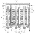
도 3 및 도 4를 참조하면, 적층 구조체들(ST)이 기판(10) 상에서 제 1 방향(D1)으로 나란히 연장되며, 제 2 방향(D2)에서 서로 이격되어 배치될 수 있다. 3 and 4 , the stacked structures ST may extend side by side on the
기판(10)은 벌크(bulk) 실리콘 기판, 실리콘-온-인슐레이터(silicon on insulator: SOI) 기판, 게르마늄 기판, 게르마늄-온-인슐레이터(germanium on insulator: GOI) 기판, 실리콘-게르마늄 기판, 또는 선택적 에피택시얼 성장(selective epitaxial growth: SEG)을 수행하여 획득한 에피택시얼 박막의 기판일 수 있다. 기판(10)은 반도체 물질로 이루어질 수 있으며, 예를 들어, 실리콘(Si), 게르마늄(Ge), 실리콘 게르마늄(SiGe), 갈륨비소(GaAs), 인듐갈륨비소(InGaAs), 알루미늄갈륨비소(AlGaAs), 또는 이들의 혼합물 중 적어도 하나를 포함할 수 있다.
적층 구조체들(ST) 각각은 기판(10) 상에 수직적으로 적층된 전극들(EL)과 이들 사이에 개재된 절연막들(ILD)을 포함한다. 적층 구조체들(ST)에서 절연막들(ILD)의 두께는 반도체 메모리 소자의 특성에 따라 달라질 수 있다. 일 예로 절연막들(ILD)은 실질적으로 동일한 두께를 가질 수 있으며, 최하층의 절연막(ILD)의 두께는 다른 절연막들(ILD)보다 얇을 수 있다. 또한, 절연막들(ILD) 중 일부는 다른 절연막들(ILD)보다 두껍게 형성될 수도 있다. Each of the stack structures ST includes electrodes EL vertically stacked on the
실시예들에 따르면, 절연막들(ILD)은 실리콘 산화막보다 유전 상수가 낮은 유전물질로 형성될 수 있으며, 적어도 하나 이상의 막들로 구성될 수 있다. 절연막들(ILD)은 약 1.0 내지 3.0의 유전 상수를 가질 수 있으며, 유기, 무기 및 유기-무기 하이브리드 물질 중 적어도 하나를 포함할 수 있다. 또한, 절연막들(ILD)은 다공성(porous) 절연막 또는 비다공성(non-porous) 절연막일 수 있다. In example embodiments, the insulating layers ILD may be formed of a dielectric material having a lower dielectric constant than that of a silicon oxide layer, and may include at least one layer. The insulating layers ILD may have a dielectric constant of about 1.0 to 3.0, and may include at least one of organic, inorganic, and organic-inorganic hybrid materials. Also, the insulating layers ILD may be a porous insulating layer or a non-porous insulating layer.
일 예로, 절연막들(ILD)은 불순물이 도우프된 산화막 계열로 형성될 수 있다. 예를 들어, 불순물이 도우프된 산화막 계열로는 불소가 도핑된 산화막(fluorine-doped oxide 또는 FSG), 탄소가 도핑된 산화막, 실리콘 산화막, HSQ(hydrogen silsesquioxane; SiO:H), MSQ(methyl silsesquioxane; SiO:CH3) 또는 a-SiOC(SiOC:H) 등으로 형성할 수 있다. 다른 예로, 절연막들(ILD)은 저유전율(Low-k)을 갖는 유기폴리머로 형성될 수도 있다. 예를 들어, 저유전율을 갖는 유기폴리머는 폴리알릴에테르계 수지, 환상 불소 수지, 실록산 공중합체, 불화 폴리알릴에테르계 수지, 폴리펜타플루오르스티렌(polypentafluorostylene), 폴리테트라플루오르스티렌계 수지, 불화 폴리이미드 수지, 불화 폴리나프탈렌(polynaphthalene fluride), 폴리사이드(polycide) 수지 등일 수 있다. For example, the insulating layers ILD may be formed of an oxide layer type doped with impurities. For example, as an impurity-doped oxide film series, fluorine-doped oxide (FSG), carbon-doped oxide, silicon oxide, HSQ (hydrogen silsesquioxane; SiO:H), MSQ (methyl silsesquioxane) ; SiO:CH3) or a-SiOC (SiOC:H). As another example, the insulating layers ILD may be formed of an organic polymer having a low dielectric constant (Low-k). For example, the organic polymer having a low dielectric constant includes a polyallyl ether-based resin, a cyclic fluororesin, a siloxane copolymer, a fluorinated polyallyl ether-based resin, a polypentafluorostylene, a polytetrafluorostyrene-based resin, and a fluorinated polyimide. It may be a resin, polynaphthalene fluoride (polynaphthalene fluride), polycide resin, or the like.
실시예들에 따르면, 적층 구조체들(ST)을 구성하는 절연막들(ILD)의 유전율을 감소시킴으로써, 3차원 반도체 메모리 장치의 동작시 수직적으로 적층된 전극들(EL) 간의 기생 캐패시턴스를 줄일 수 있다. 본 발명의 실시예들에 따른 절연막들(ILD)의 다양한 실시예들에 대해 도 5a 내지 도 5e 및 도 6a 및 도 6b를 참조하여 보다 상세히 설명한다. In example embodiments, by reducing the dielectric constant of the insulating layers ILD constituting the stack structures ST, parasitic capacitance between the vertically stacked electrodes EL may be reduced when the 3D semiconductor memory device is operated. . Various embodiments of the insulating layers ILD according to embodiments of the present invention will be described in more detail with reference to FIGS. 5A to 5E and FIGS. 6A and 6B .
실시예들에 따르면, 수직 구조체들(VS)은 적층 구조체들(ST) 각각을 관통하여 기판(10)에 연결될 수 있다. 일 예로, 수직 구조체들(VS)은 반도체 물질을 포함할 수 있다. 수직 구조체들(VS)의 바닥면들은 기판(10)의 상부면과 하부면 사이에 위치할 수 있다. 수직 구조체들(VS)의 상단에는 비트라인 콘택 플러그(BPLG)와 접속되는 콘택 패드가 위치할 수 있다. In example embodiments, the vertical structures VS may pass through each of the stack structures ST to be connected to the
일 예로, 수직 구조체들(VS) 각각은, 도 5a 내지 도 5e와, 도 6a 및 도 6b에 도시된 바와 같이, 기판(10)과 접촉하는 제 1 반도체 패턴(SP1) 및 제 1 반도체 패턴(SP1)과 데이터 저장막(DS) 사이에 개재되는 제 2 반도체 패턴(SP2)을 포함할 수 있다. 제 1 반도체 패턴(SP1)는 원 기둥(pillar) 형태일 수 있으며, 이와 달리, 제 1 반도체 패턴(SP1)은 속이 빈 파이프 형태(pipe-shaped) 또는 마카로니 형태(macaroni-shaped)일 수 있다. 제 1 반도체 패턴(SP1)의 하단은 닫힌 상태(closed state)일 수 있으며, 제 1 반도체 패턴(SP1)의 내부는 매립 절연 패턴(VI)에 의해 채워질 수 있다. 제 1 반도체 패턴(SP1)은 제 2 반도체 패턴(SP2)의 내벽과 기판(10)과 상부면과 접촉될 수 있다. 즉, 제 1 반도체 패턴(SP1)은 제 2 반도체 패턴(SP2)과 기판(10)을 전기적으로 연결할 수 있다. 그리고, 제 1 반도체 패턴(SP1)의 바닥면은 기판(10)의 상부면보다 낮은 레벨에 위치할 수 있다. 제 2 반도체 패턴(SP2)은 상단 및 하단이 오픈된(opened) 파이프 형태 또는 마카로니 형태일 수 있다. 제 1 및 제 2 반도체 패턴들(SP1, SP2)은 언도프트 상태이거나, 기판(10)과 동일한 도전형을 갖는 불순물로 도핑될 수 있다. 제 1 반도체 패턴(SP1)과 제 2 반도체 패턴(SP2)은 다결정 상태 또는 단결정 상태일 수 있다.For example, each of the vertical structures VS includes a first semiconductor pattern SP1 and a first semiconductor pattern SP1 in contact with the
데이터 저장막(DS)이 적층 구조체들(ST)과 수직 구조체들(VS) 사이에 배치될 수 있다. 데이터 저장막(DS)은 적층 구조체들(ST)을 관통하는 수직 절연 패턴(VP)과, 전극들(EL)과 수직 절연 패턴(VP) 사이에서 전극들(EL)의 상부면들 및 하부면들로 연장되는 수평 패턴(HP)을 포함할 수 있다. 일 예로, 데이터 저장막(DS)의 수직 절연 패턴(VP)은, 도 6a 및 도 6b에 도시된 바와 같이, 수직 구조체들(VS)의 측벽들을 감싸며, 기판(10)과 직접 접촉할 수 있다. 본 발명의 실시예들에 따른 데이터 저장막(DS)에 대해서는 도 7a 내지 도 7e를 참조하여 보다 상세히 후술하기로 한다.The data storage layer DS may be disposed between the stacked structures ST and the vertical structures VS. The data storage layer DS includes a vertical insulating pattern VP passing through the stacked structures ST, and upper and lower surfaces of the electrodes EL between the electrodes EL and the vertical insulating pattern VP. It may include a horizontal pattern (HP) extending to the. For example, the vertical insulating pattern VP of the data storage layer DS may surround sidewalls of the vertical structures VS and may directly contact the
공통 소오스 영역들(CSR)은 각각 서로 인접하는 적층 구조체들(ST) 사이에서 기판(10) 내에 배치될 수 있다. 공통 소오스 영역들(CSR)은 적층 구조체들(ST)과 나란하게 제 1 방향(D1)으로 연장될 수 있다. 공통 소오스 영역들(CSR)은 기판(10) 내에 제 2 도전형의 불순물을 도핑하여 형성될 수 있다. 공통 소오스 영역들(CSR)은 예를 들어, N형의 불순물(예를 들어, 비소(As) 또는 인(P))을 포함할 수 있다.The common source regions CSR may be disposed in the
공통 소오스 플러그(CSP)가 공통 소오스 영역(CSR)에 접속될 수 있으며, 공통 소오스 플러그(CSP)와 적층 구조체들(ST) 사이에 측벽 절연 스페이서(SP)가 개재될 수 있다. 일 예로, 공통 소오스 플러그(CSP)는 실질적으로 균일한 상부 폭을 가지며, 제 1 방향(D1)으로 나란히 연장될 수 있다. 측벽 절연 스페이서(SP)는 서로 인접하는 적층 구조체들(ST) 사이에서 서로 대향하여 배치될 수 있다. 다른 예로, 측벽 절연 스페이서(SP)는 서로 인접하는 적층 구조체들(ST) 사이를 채울 수 있으며, 공통 소오스 플러그(CSP)가 측벽 절연 스페이서(SP)를 관통하여 공통 소오스 영역(CSR)과 국소적으로 접속될 수 있다. The common source plug CSP may be connected to the common source region CSR, and a sidewall insulating spacer SP may be interposed between the common source plug CSP and the stack structures ST. For example, the common source plug CSP may have a substantially uniform upper width and may extend side by side in the first direction D1 . The sidewall insulating spacers SP may be disposed to face each other between the stacked structures ST adjacent to each other. As another example, the sidewall insulating spacer SP may fill between the stacked structures ST adjacent to each other, and the common source plug CSP penetrates the sidewall insulating spacer SP to form a local area with the common source region CSR. can be connected to
상부 매립 절연막(120) 및 캡핑 절연막(125)이 복수의 적층 구조체들(ST)을 덮으며, 캡핑 절연막(125) 상에 적층 구조체들(ST)을 가로질러 제 2 방향(D2)으로 연장되는 비트 라인들(BL)이 배치될 수 있다. 비트 라인들(BL)은 비트라인 콘택 플러그(BPLG)를 통해 수직 구조체(VS)와 전기적으로 연결될 수 있다. The upper filling insulating
일 예에서, 3차원 반도체 메모리 장치는 수직형 낸드 플래시 메모리 장치일 수 있으며, 이 경우, 전극들(EL)은 메모리 셀 트랜지스터들(도 2의 MCT)의 제어 게이트 전극들로 사용될 수 있다. 예를 들면, 최상층의 전극(EL) 및 최하층의 전극(EL) 사이의 전극들(EL)은 제어 게이트 전극들 및 이들을 연결하는 워드 라인들로써 사용될 수 있다. 전극들(EL)은 수직 구조체들(VS)과 결합하여 메모리 셀 트랜지스터들(도 2의 MCT)을 구성할 수 있다. 적층 구조체들(ST)에서, 최하층 및 최상층의 전극들(EL)은 선택 트랜지스터들(도 2의 SST, GST)의 게이트 전극들로 이용될 수 있다. 예를 들면, 최상층의 전극(EL)은 비트 라인(BL)과 수직 구조체들(VS) 사이의 전기적 연결을 제어하는 스트링 선택 트랜지스터(도 2의 SST)의 게이트 전극으로 사용되고, 최하층의 전극(EL)은 공통 소오스 영역(CSR)과 수직 구조체들(VS) 사이의 전기적 연결을 제어하는 접지 선택 트랜지스터(도 2의 GST)의 게이트 전극으로 사용될 수 있다. 또한, 도 2에 도시된 3차원 반도체 메모리 장치의 읽기 또는 프로그램 동작시 공통 소오스 플러그(CSP)를 통해 공통 소오스 영역(CSR)에 접지 전압이 인가될 수 있다.In one example, the 3D semiconductor memory device may be a vertical NAND flash memory device, and in this case, the electrodes EL may be used as control gate electrodes of the memory cell transistors (MCT of FIG. 2 ). For example, the electrodes EL between the uppermost electrode EL and the lowermost electrode EL may be used as control gate electrodes and word lines connecting them. The electrodes EL may be combined with the vertical structures VS to form memory cell transistors (MCT of FIG. 2 ). In the stack structures ST, the electrodes EL of the lowermost layer and the uppermost layer may be used as gate electrodes of the selection transistors SST and GST of FIG. 2 . For example, the uppermost electrode EL is used as a gate electrode of a string select transistor (SST of FIG. 2 ) that controls the electrical connection between the bit line BL and the vertical structures VS, and the lowermost electrode EL ) may be used as a gate electrode of a ground selection transistor (GST of FIG. 2 ) that controls an electrical connection between the common source region CSR and the vertical structures VS. Also, a ground voltage may be applied to the common source region CSR through the common source plug CSP during a read or program operation of the 3D semiconductor memory device illustrated in FIG. 2 .
이러한 3차원 반도체 메모리 장치에서, 절연막들(ILD) 중 적어도 하나 이상은 산화막보다 유전상수가 낮은 저유전막일 수 있으며, 예를 들어, 절연막들(ILD)은 기공들(pores; P)을 포함하는 다공성(porous) 저유전막을 포함할 수 있다. 일 예에서, 기공들(P)을 포함하는 절연막들(ILD)은 기공 형성 물질(pore generator), 즉, 포로젠(porogen)을 포함하는 절연막들을 형성한 후, 절연막들 내에서 포로젠을 제거하여 형성될 수 있다. 절연막들(ILD) 내에서 기공들(P)의 크기(예를 들면, 직경)는 수 내지 수백 nm일 수 있다. 다공성 저유전막은 기공(pore)의 사이즈가 커지면 커질수록 유전상수인 k값이 낮아짐에 따라 수직적으로 인접하는 전극들(EL) 간의 기생 캐패시턴스를 줄일 수 있다. 예를 들어, 다공성 저유전막은 SiOCH막, SiOC막 및 SiOF막으로 이루어진 그룹에서 선택된 적어도 어느 하나일 수 있다. 다공성 저유전막에서 기공들의 크기(예를 들면, 직경)는 수십 내지 수백 nm일 수 있다. 예를 들어, 다공성 저유전막은 5~50vol%의 기공도(porosity)를 가질 수 있다.In such a 3D semiconductor memory device, at least one of the insulating layers ILD may be a low-k layer having a lower dielectric constant than that of the oxide layer, and for example, the insulating layers ILD may include pores (P). It may include a porous low-k film. In one example, the insulating layers ILD including the pores P are formed with a pore generator, that is, insulating layers including porogen, and then the porogen is removed from the insulating layers. can be formed by The size (eg, diameter) of the pores P in the insulating layers ILD may be several to several hundred nm. In the porous low-k film, as the size of the pores increases, the k value, which is the dielectric constant, decreases, so that the parasitic capacitance between the vertically adjacent electrodes EL may be reduced. For example, the porous low-k film may be at least one selected from the group consisting of an SiOCH film, an SiOC film, and an SiOF film. The size (eg, diameter) of the pores in the porous low-k film may be tens to hundreds of nm. For example, the porous low-k film may have a porosity of 5 to 50 vol%.
한편, 적층 구조체들(ST)을 구성하는 전극들(EL) 및 절연막들(ILD)은 인장 스트레스(tensile stress) 및 압축 스트레스(compressive stress)를 가지며, 이로 인해 전극들(EL) 및 절연막들(ILD)의 적층 수가 증가함에 따라, 기판(10)에 가해지는 스트레스가 증가할 수 있다. 이로 인해 기판(10)이 휘어지는 현상 등이 발생할 수 있다. 한편, 적층 구조체들(ST)을 구성하는 절연막들(ILD) 적어도 하나 이상은 기공들을 포함하므로, 절연막들(ILD)의 스트레스가 감소될 수 있다. Meanwhile, the electrodes EL and the insulating layers ILD constituting the stacked structures ST have tensile stress and compressive stress, and thus the electrodes EL and the insulating layers ILD As the number of stacked ILDs increases, the stress applied to the
도 5a 내지 도 5e를 참조하면, 적층 구조체들(ST)을 구성하는 일부 절연막들(ILD)의 두께(t1)는, 각 전극들(EL)의 두께(t2)보다 작을 수 있다. 일 예에서, 적층 구조체들(ST)에서 각 절연막들(ILD)의 수평적 두께(즉, 수직 구조체(VS)의 측벽으로부터 공통 소오스 플러그(CSP)에 인접한 절연막(ILD)의 측벽까지의 거리)는 각 전극들(EL)의 수평적 두께보다 클 수 있다. 이에 따라, 공통 소오스 플러그(CSP)에 인접한 적층 구조체(ST)의 측벽은 복수의 리세스 영역들을 가질 수 있다. 여기서, 리세스 영역들 각각은 수직적으로 인접한 절연막들(ILD) 및 이들 사이에 개재된 전극(EL)에 의해 정의될 수 있으며, 리세스 영역들은 측벽 절연 스페이서(SP)에 의해 채워질 수 있다. 다른 실시예에서, 수직 구조체(VS)의 일측벽으로부터 전극들(EL)의 수평적 두께 및 절연막들(ILD)의 수평적 두께는 실질적으로 동일할 수도 있다. Referring to FIGS. 5A to 5E , a thickness t1 of some insulating layers ILD constituting the stack structures ST may be smaller than a thickness t2 of each of the electrodes EL. In one example, the horizontal thickness of each of the insulating layers ILD in the stacked structures ST (ie, the distance from the sidewall of the vertical structure VS to the sidewall of the insulating layer ILD adjacent to the common source plug CSP)) may be greater than the horizontal thickness of each of the electrodes EL. Accordingly, the sidewall of the stack structure ST adjacent to the common source plug CSP may have a plurality of recess regions. Here, each of the recess regions may be defined by vertically adjacent insulating layers ILD and an electrode EL interposed therebetween, and the recess regions may be filled with sidewall insulating spacers SP. In another embodiment, the horizontal thickness of the electrodes EL and the horizontal thickness of the insulating layers ILD from one sidewall of the vertical structure VS may be substantially the same.
절연막들(ILD)은 기공들(P)을 포함하며, 데이터 저장막(DS)을 구성하는 막들(예를 들어, 수평 절연 패턴(HP))보다 작은 유전율을 가질 수 있다. 또한, 절연막들(ILD)의 유전율은 측벽 절연 스페이서(SP)의 유전율보다 작을 수 있다. The insulating layers ILD include pores P, and may have a dielectric constant smaller than that of layers (eg, the horizontal insulating pattern HP) constituting the data storage layer DS. Also, the dielectric constant of the insulating layers ILD may be smaller than that of the sidewall insulating spacer SP.
도 5b에 도시된 실시예에 따르면, 절연막들(ILD) 각각은 수직 구조체들(VS)과 인접한 제 1 측벽(S1)과 공통 소오스 플러그(CSP)와 인접한 제 2 측벽(S2)을 가질 수 있다. 여기서, 제 2 측벽(S2)은 기공들(P)이 노출되어 형성된 그루브들을 가질 수 있으며, 그루브들은 측벽 절연 스페이서(SP)에 의해 채워질 수 있다. 즉, 기공들(P)을 포함하는 절연막들(ILD)은 울퉁불퉁한 제 2 측벽(S2)을 가질 수 있다. 5B , each of the insulating layers ILD may have a first sidewall S1 adjacent to the vertical structures VS and a second sidewall S2 adjacent to the common source plug CSP. . Here, the second sidewall S2 may have grooves formed by exposing the pores P, and the grooves may be filled by the sidewall insulating spacers SP. That is, the insulating layers ILD including the pores P may have an uneven second sidewall S2 .
도 5c, 도 5d, 및 도 5e에 도시된 실시예에 따르면, 적층 구조체(ST)를 구성하는 각각의 절연막들(ILD)은 제 1 유전막들(DIL1) 및 제 2 유전막(DIL2)을 포함할 수 있으며, 제 1 유전막들(DIL1) 및 제 2 유전막(DIL2)은 수직적으로 인접하는 전극들(EL) 사이에 배치될 수 있다. 5C, 5D, and 5E, each of the insulating layers ILD constituting the stacked structure ST may include the first dielectric layers DIL1 and the second dielectric layer DIL2. The first and second dielectric layers DIL1 and DIL2 may be disposed between vertically adjacent electrodes EL.
일 예로, 수직적으로 인접하는 전극들 사이에 제 1 유전막들(DIL1)이 배치될 수 있으며, 제 1 유전막들(DIL1) 사이에 제 2 유전막(DIL2)이 배치될 수 있다. 도시된 바와 같이, 제 1 유전막(DIL1)과 제 2 유전막(DIL2)은 서로 다른 두께를 가질 수 있으며, 이와 달리, 실질적으로 동일한 두께를 가질 수도 있다. For example, first dielectric layers DIL1 may be disposed between vertically adjacent electrodes, and second dielectric layers DIL2 may be disposed between first dielectric layers DIL1 . As illustrated, the first dielectric layer DIL1 and the second dielectric layer DIL2 may have different thicknesses, or alternatively, may have substantially the same thickness.
일 예에서, 제 1 유전막(DIL1)과 제 2 유전막(DIL2)은 서로 다른 유전율(dielectric constant)을 가질 수 있다. 예를 들어, 도 5c에 도시된 바와 같이, 제 1 유전막들(DIL1)은 다공성 저유전막일 수 있으며, 제 2 유전막(DIL2)은 비다공성 저유전막일 수 있다. 제 1 유전막들(DIL1)의 유전율은 제 2 유전막(DIL2)의 유전율보다 작을 수 있다.In one example, the first dielectric layer DIL1 and the second dielectric layer DIL2 may have different dielectric constants. For example, as shown in FIG. 5C , the first dielectric films DIL1 may be porous low-k films, and the second dielectric films DIL2 may be non-porous low-k films. The dielectric constant of the first dielectric layers DIL1 may be less than that of the second dielectric layer DIL2 .
기공들(P)을 포함하는 다공성 저유전막은 비다공성 저유전막보다 압축 스트레스가 감소될 수 있다. 즉, 제 1 유전막들(DIL1)의 압축 스트레스는 제 2 유전막(DIL2)의 압축 스트레스보다 작을 수 있다. 즉, 기공들(P)을 포함하는 다공성 저유전막들 사이에 비다공성 유전막을 배치함으로써, 수직적으로 인접하는 전극들(EL)이 무너지는 것을 방지할 수 있다. The porous low-k membrane including the pores P may have reduced compressive stress than the non-porous low-k membrane. That is, the compressive stress of the first dielectric layers DIL1 may be less than the compressive stress of the second dielectric layers DIL2 . That is, by disposing the non-porous dielectric film between the porous low-k films including the pores P, it is possible to prevent the vertically adjacent electrodes EL from collapsing.
도 5d를 참조하면, 제 1 및 제 2 유전막들(DIL1, DIL2)은 기공들(P)을 포함하되, 제 1 유전막들(DIL1)의 기공도(porosity)가 제 2 유전막(DIL2)의 기공도보다 클 수 있다. 즉, 제 1 유전막들(DIL1)의 유전율은 제 2 유전막(DIL2)의 유전율보다 작을 수 있다. Referring to FIG. 5D , the first and second dielectric layers DIL1 and DIL2 include pores P, and the porosity of the first dielectric layers DIL1 is the porosity of the second dielectric layer DIL2. may be larger than That is, the dielectric constant of the first dielectric layers DIL1 may be smaller than that of the second dielectric layer DIL2 .
도 5e를 참조하면, 제 1 및 제 2 유전막들(DIL1, DIL2)은 기공들(P)을 포함하되, 제 1 유전막들(DIL1) 내의 기공들(P)의 크기가 제 2 유전막(DIL2) 내의 기공들(P)의 크기보다 작을 수 있다. Referring to FIG. 5E , the first and second dielectric layers DIL1 and DIL2 include pores P, and the size of the pores P in the first dielectric layers DIL1 is the second dielectric layer DIL2. It may be smaller than the size of the pores (P) in the.
도 6a, 도 6b, 및 도 6c를 참조하면, 적층 구조체들(ST)을 구성하는 절연막들은 제 1 두께(t1)를 갖는 제 2 절연막(ILD2)과 제 1 두께(t1)보다 큰 제 3 두께(t3)를 갖는 제 1 절연막(ILD1)을 포함할 수 있다. 제 1 절연막(ILD1)과 제 2 절연막(ILD2) 사이의 전극(EL)은 제 1 두께(t1)보다 크고 제 3 두께(t3)보다 작은 제 2 두께(t2)를 가질 수 있다. 일 예에서, 제 1 절연막(ILD1)은 워드 라인(도 2의 WL)으로 사용되는 전극(EL)과 접지 선택 라인(도 2의 GSL) 또는 스트링 선택 라인(도 2의 SSL)으로 사용되는 전극(EL) 사이에 배치될 수 있다. 그리고, 제 2 절연막(ILD2)은 워드 라인들(도 2의 WL)으로 사용되는 전극들(EL) 사이에 배치될 수 있다. 6A, 6B, and 6C , the insulating layers constituting the stacked structures ST include a second insulating layer ILD2 having a first thickness t1 and a third thickness greater than the first thickness t1. A first insulating layer ILD1 having (t3) may be included. The electrode EL between the first insulating layer ILD1 and the second insulating layer ILD2 may have a second thickness t2 greater than the first thickness t1 and smaller than the third thickness t3 . In an example, the first insulating layer ILD1 includes an electrode EL used as a word line (WL of FIG. 2 ) and an electrode used as a ground selection line (GSL of FIG. 2 ) or a string selection line (SSL of FIG. 2 ). (EL) may be disposed between. In addition, the second insulating layer ILD2 may be disposed between the electrodes EL used as word lines (WL of FIG. 2 ).
도 6a를 참조하면, 제 1 및 제 2 절연막들(ILD1, ILD2)은 기공들(P)을 포함할 수 있다. 제 1 및 제 2 절연막들(ILD1, ILD2) 내에서 기공들(P)의 크기는 실질적으로 동일할 수 있다. 다시 말해, 제 1 및 제 2 절연막들(ILD1, ILD2)에서 기공도(porosity)는 실질적으로 동일할 수 있다. 이와 달리, 도 6b를 참조하면, 제 1 절연막(ILD1)은 제 1 기공들(P1)을 가질 수 있으며, 제 2 절연막(ILD2)은 제 1 기공들(P1)보다 작은 제 2 기공들(P2)을 가질 수 있다. 기공들의 크기 차이에 의해 제 1 및 제 2 절연막들(ILD1, ILD2)은 동일한 유전 물질로 이루어지되, 서로 다른 유전 상수를 가질 수 있다. 다른 예로, 도 6c를 참조하면, 제 1 절연막(ILD1)은 비다공성막일 수 있으며, 제 2 절연막(ILD2)은 다공성막일 수 있다. Referring to FIG. 6A , the first and second insulating layers ILD1 and ILD2 may include pores P. The size of the pores P in the first and second insulating layers ILD1 and ILD2 may be substantially the same. In other words, the porosity of the first and second insulating layers ILD1 and ILD2 may be substantially the same. Alternatively, referring to FIG. 6B , the first insulating layer ILD1 may have first pores P1 , and the second insulating layer ILD2 may have second pores P2 smaller than the first pores P1 . ) can have Due to the size difference of the pores, the first and second insulating layers ILD1 and ILD2 may be made of the same dielectric material, but may have different dielectric constants. As another example, referring to FIG. 6C , the first insulating film ILD1 may be a non-porous film, and the second insulating film ILD2 may be a porous film.
도 7a 내지 도 7e를 참조하여, 본 발명의 다양한 실시예들에 따른 데이터 저장막에 대해 상세히 설명한다. A data storage layer according to various embodiments of the present invention will be described in detail with reference to FIGS. 7A to 7E .
실시예들에 따르면, 3차원 반도체 메모리 장치는 낸드 플래시 메모리 장치일 수 있다. 예를 들어, 적층 구조체(ST)와 수직 구조체(VS) 사이에 개재되는 데이터 저장막(DS)은 터널 절연막(TL), 전하 저장막(CIL) 및 블록킹 절연막(BK)을 포함할 수 있다. 이러한 데이터 저장막(DS)에 저장되는 데이터는 반도체 물질을 포함하는 데이터 저장막 수직 구조체(VS)와 전극들(EL) 사이의 전압 차이에 의해 유발되는 파울러-노던하임 터널링을 이용하여 변경될 수 있다. In some embodiments, the 3D semiconductor memory device may be a NAND flash memory device. For example, the data storage layer DS interposed between the stacked structure ST and the vertical structure VS may include a tunnel insulating layer TL, a charge storage layer CIL, and a blocking insulating layer BK. Data stored in the data storage layer DS may be changed using Fowler-Northernheim tunneling caused by a voltage difference between the electrodes EL and the data storage layer vertical structure VS including a semiconductor material. have.
도 7a 에 도시된 실시예에 따르면, 터널 절연막(TIL), 전하 저장막(CIL), 및 블록킹 절연막(BLK)은 전극들(EL)과 수직 구조체(VS) 사이에서 층간 절연막(ILD)과 수직 구조체(VS) 사이로 연장될 수 있다. 즉, 층간 절연막(ILD)이 전극과 직접 접촉할 수 있다. 7A , the tunnel insulating layer TIL, the charge storage layer CIL, and the blocking insulating layer BLK are perpendicular to the interlayer insulating layer ILD between the electrodes EL and the vertical structure VS. It may extend between the structures VS. That is, the interlayer insulating layer ILD may directly contact the electrode.
도 7b에 도시된 실시예에 따르면, 터널 절연막(TIL) 및 전하 저장막(CIL)은 전극들(EL)과 수직 구조체(VS) 사이에서 층간 절연막(ILD)과 수직 구조체(VS) 사이로 연장될 수 있다. 그리고, 블록킹 절연막(BLK)은 전극들(EL)과 수직 구조체(VS) 사이에서 전극들(EL)의 상부면들 및 하부면들로 연장될 수 있다.According to the embodiment shown in FIG. 7B , the tunnel insulating layer TIL and the charge storage layer CIL may extend between the electrodes EL and the vertical structure VS and between the interlayer insulating layer ILD and the vertical structure VS. can In addition, the blocking insulating layer BLK may extend to upper and lower surfaces of the electrodes EL between the electrodes EL and the vertical structure VS.
도 7c에 도시된 실시예에 따르면, 터널 절연막(TIL)이 전극들(EL)과 수직 구조체(VS) 사이에서 층간 절연막(ILD)과 수직 구조체(VS) 사이로 연장될 수 있으며, 전하 저장막(CIL) 및 블록킹 절연막(BLK)은 전극들(EL)과 수직 구조체(VS) 사이에서 전극들(EL)의 상부면들 및 하부면들로 연장될 수 있다.According to the embodiment shown in FIG. 7C , the tunnel insulating film TIL may extend between the interlayer insulating film ILD and the vertical structure VS between the electrodes EL and the vertical structure VS, and the charge storage film ( CIL) and the blocking insulating layer BLK may extend to upper and lower surfaces of the electrodes EL between the electrodes EL and the vertical structure VS.
도 7d에 도시된 실시예에 따르면, 터널 절연막(TIL), 전하 저장막(CIL) 및 블록킹 절연막(BLK)은 전극들(EL)과 수직 구조체(VS) 사이에서 전극들(EL)의 상부면들 및 하부면들로 연장될 수 있다.According to the embodiment shown in FIG. 7D , the tunnel insulating layer TIL, the charge storage layer CIL, and the blocking insulating layer BLK are formed between the electrodes EL and the vertical structure VS on the upper surfaces of the electrodes EL. may extend to the poles and lower surfaces.
도 7e에 도시된 실시예에 따르면, 데이터 저장막(DS)은 서로 다른 물질로 이루어진 제 1 및 제 2 블록킹 절연막들(BLK1, BLK2)을 포함할 수 있다. 터널 절연막(TIL), 전하 저장막(CIL), 및 제 1 블록킹 절연막(BLK1)은 전극들(EL)과 수직 구조체(VS) 사이에서 층간 절연막(ILD)과 수직 구조체(VS) 사이로 수직적으로 연장될 수 있다. 그리고, 제 2 블록킹 절연막(BLK2)이 전극들(EL)과 제 1 블록킹 절연막(BLK1) 사이에서 전극들(EL)의 상부면들 및 하부면들로 수평적으로 연장될 수 있다.According to the embodiment illustrated in FIG. 7E , the data storage layer DS may include first and second blocking insulating layers BLK1 and BLK2 made of different materials. The tunnel insulating layer TIL, the charge storage layer CIL, and the first blocking insulating layer BLK1 extend vertically between the electrodes EL and the vertical structure VS between the interlayer insulating layer ILD and the vertical structure VS. can be In addition, the second blocking insulating layer BLK2 may horizontally extend between the electrodes EL and the first blocking insulating layer BLK1 to upper and lower surfaces of the electrodes EL.
도 7a 내지 도 7e에 도시된 데이터 저장막에서, 전하저장막(CIL)은 트랩 사이트들이 풍부한 절연막들 및 나노 입자들을 포함하는 절연막들 중의 한가지일 수 있으며, 화학 기상 증착 또는 원자층 증착 기술들 중의 한가지를 사용하여 형성될 수 있다. 예를 들면, 전하저장막(CIL)은 트랩 절연막, 부유 게이트 전극 또는 도전성 나노 돗들(conductive nano dots)을 포함하는 절연막 중의 한가지를 포함할 수 있다. 더 구체적인 예로, 전하저장막(CIL)은 실리콘 질화막, 실리콘 산화질화막, 실리콘-풍부 질화막(Si-rich nitride), 나노크리스탈 실리콘(nanocrystalline Si) 및 박층화된 트랩막(laminated trap layer) 중의 적어도 하나를 포함할 수 있다. In the data storage film shown in FIGS. 7A to 7E , the charge storage film (CIL) may be one of insulating films rich in trap sites and insulating films including nanoparticles, and is one of chemical vapor deposition or atomic layer deposition techniques. It can be formed using one. For example, the charge storage layer CIL may include one of a trap insulating layer, a floating gate electrode, or an insulating layer including conductive nano dots. As a more specific example, the charge storage layer (CIL) may include at least one of a silicon nitride layer, a silicon oxynitride layer, a silicon-rich nitride layer, a nanocrystalline silicon layer, and a laminated trap layer. may include.
터널 절연막(TIL)은 전하저장막(CIL)보다 큰 밴드 갭을 갖는 물질들 중의 한가지일 수 있으며, 화학 기상 증착 또는 원자층 증착 기술들 중의 한가지를 사용하여 형성될 수 있다. 예를 들면, 터널 절연막(TIL)은 상술한 증착 기술들 중의 하나를 사용하여 형성되는 실리콘 산화막일 수 있다. 이와 달리, 터널 절연막은 알루미늄 산화막 및 하프늄 산화막 등과 같은 고유전막들 중의 하나일 수 있다.The tunnel insulating layer TIL may be one of materials having a larger band gap than the charge storage layer CIL, and may be formed using either chemical vapor deposition or atomic layer deposition techniques. For example, the tunnel insulating layer TIL may be a silicon oxide layer formed using one of the deposition techniques described above. Alternatively, the tunnel insulating layer may be one of high-k layers such as an aluminum oxide layer and a hafnium oxide layer.
블록킹 절연막(BLK)은 터널 절연막(TIL)보다 작고 전하 저장막(CIL)보다 큰 밴드 갭을 갖는 물질들 중의 한가지일 수 있다. 블록킹 절연막(BLK)은 알루미늄 산화막 및 하프늄 산화막 등과 같은 고유전막들을 포함할 수 있다. 블록킹 절연막(BLK)은 화학 기상 증착 또는 원자층 증착 기술들 중의 한가지를 사용하여 형성될 수 있으며, 이들 중의 적어도 하나는 습식 산화 공정을 통해 형성될 수 있다. The blocking insulating layer BLK may be one of materials having a band gap smaller than the tunnel insulating layer TIL and larger than the charge storage layer CIL. The blocking insulating layer BLK may include high-k layers such as an aluminum oxide layer and a hafnium oxide layer. The blocking insulating layer BLK may be formed using one of chemical vapor deposition or atomic layer deposition techniques, and at least one of these may be formed through a wet oxidation process.
도 7e에 도시된 바와 같이, 데이터 저장막(DS)이 제 1 및 제 2 블록킹 절연막들(BLK1, BLK2)을 포함하는 경우, 일 예로, 제 1 블록킹 절연막(BLK1)은 알루미늄 산화막 및 하프늄 산화막 등과 같은 고유전막들 중의 하나이고, 제 2 블록킹 절연막(BLK2)은 제 1 블록킹 절연막(BLK1)보다 작은 유전 상수를 갖는 물질일 수 있다. 다른 예로, 제 2 블록킹 절연막(BLK2)은 고유전막들 중의 하나이고, 제 1 블록킹 절연막(BLK1)은 제 2 블록킹 절연막(BLK2)보다 작은 유전 상수를 갖는 물질일 수 있다. As shown in FIG. 7E , when the data storage layer DS includes the first and second blocking insulating layers BLK1 and BLK2 , for example, the first blocking insulating layer BLK1 may include an aluminum oxide layer, a hafnium oxide layer, and the like. One of the same high-k films, and the second blocking insulating layer BLK2 may be a material having a smaller dielectric constant than that of the first blocking insulating layer BLK1 . As another example, the second blocking insulating layer BLK2 may be one of high dielectric layers, and the first blocking insulating layer BLK1 may be made of a material having a smaller dielectric constant than that of the second blocking insulating layer BLK2 .
도 7a 내지 도 7e를 참조하여 설명된 데이터 저장막(DS)에 저장되는 데이터는 반도체 물질을 포함하는 수직 구조체(VS)와 전극들(EL) 사이의 전압 차이에 의해 유발되는 파울러-노던하임 터널링을 이용하여 변경될 수 있다. 이와 달리, 데이터 저장막(DS)은 다른 동작 원리에 기초하여 정보를 저장하는 것이 가능한 박막(예를 들면, 상변화 메모리를 위한 박막 또는 가변저항 메모리를 위한 박막)일 수도 있다.Data stored in the data storage layer DS described with reference to FIGS. 7A to 7E is Fowler-Northernheim tunneling caused by a voltage difference between the electrodes EL and the vertical structure VS including a semiconductor material. can be changed using Alternatively, the data storage layer DS may be a thin film capable of storing information based on a different operating principle (eg, a thin film for a phase change memory or a thin film for a variable resistance memory).
도 8은 본 발명의 실시예들에 따른 3차원 반도체 메모리 장치의 단면도로서, 도 3의 I-I' 선을 따라 자른 단면이다. 도 9a 및 도 9b는 도 8의 A 부분을 확대한 도면들이다. 설명의 간략함을 위해, 도 4, 도 5a 내지 도 5e, 도 6a, 도 6b, 도 6c 및 도 7a 내지 도 7e를 참조하여 앞서 설명된 3차원 반도체 메모리 장치의 제조 방법과 동일한 기술적 특징들에 대한 설명은 생략될 수 있다.FIG. 8 is a cross-sectional view of a three-dimensional semiconductor memory device according to embodiments of the present invention, taken along line I-I' of FIG. 3 . 9A and 9B are enlarged views of part A of FIG. 8 . For simplicity of explanation, the same technical features as those of the manufacturing method of the three-dimensional semiconductor memory device described above with reference to FIGS. 4, 5A to 5E, 6A, 6B, 6C, and 7A to 7E. A description thereof may be omitted.
도 8, 도 9a, 및 도 9b를 참조하면, 수직 구조체들(VS) 각각은, 적층 구조체(ST)의 하부 부분을 관통하여 수평 반도체층(100)과 접속되는 하부 반도체 패턴(LSP) 및 적층 구조체(ST)의 상부 부분을 관통하여 하부 반도체 패턴(LSP)과 연결되는 상부 반도체 패턴(USP)을 포함한다. Referring to FIGS. 8, 9A, and 9B , each of the vertical structures VS includes a lower semiconductor pattern LSP connected to the
상부 반도체 패턴(USP)은 속이 빈 파이프 형태(pipe-shaped) 또는 마카로니 형태(macaroni-shaped)일 수 있다. 이때, 상부 반도체 패턴(USP)의 하단은 닫힌 상태(closed state)일 수 있다. 그리고, 상부 반도체 패턴(USP)의 내부는 매립 절연 패턴(VI)에 의해 채워질 수 있다. 그리고, 상부 반도체 패턴(USP)의 바닥면은 하부 반도체 패턴(LSP)의 상부면보다 낮은 레벨에 위치할 수 있다. 즉, 상부 반도체 패턴(USP)은 하부 반도체 패턴(LSP)에 삽입된 구조를 가질 수 있다. 상부 반도체 패턴(USP)은 반도체 물질로 이루어질 수 있다. 예를 들어, 상부 반도체 패턴(USP)은 실리콘(Si), 게르마늄(Ge) 또는 이들의 혼합물을 포함할 수 있으며, 불순물이 도핑된 반도체이거나 불순물이 도핑되지 않은 상태의 진성 반도체(intrinsic semiconductor)일 수도 있다. 또한, 상부 반도체 패턴(USP)은 단결정, 비정질(amorphous), 및 다결정(polycrystalline) 중에서 선택된 적어도 어느 하나를 포함하는 결정 구조를 가질 수 있다. 나아가, 상부 반도체 패턴(USP)은 그것의 상단에 도전 패드(PAD)를 가질 수 있다. 도전 패드(PAD)는 불순물이 도핑된 불순물 영역이거나, 도전 물질로 이루어질 수 있다. The upper semiconductor pattern USP may have a pipe-shaped shape or a macaroni-shaped shape. In this case, the lower end of the upper semiconductor pattern USP may be in a closed state. In addition, the inside of the upper semiconductor pattern USP may be filled by the buried insulating pattern VI. In addition, the bottom surface of the upper semiconductor pattern USP may be positioned at a level lower than the top surface of the lower semiconductor pattern LSP. That is, the upper semiconductor pattern USP may have a structure inserted into the lower semiconductor pattern LSP. The upper semiconductor pattern USP may be formed of a semiconductor material. For example, the upper semiconductor pattern USP may include silicon (Si), germanium (Ge), or a mixture thereof, and may be a semiconductor doped with an impurity or an intrinsic semiconductor in an undoped state. may be Also, the upper semiconductor pattern USP may have a crystal structure including at least one selected from single crystal, amorphous, and polycrystalline. Furthermore, the upper semiconductor pattern USP may have a conductive pad PAD on its upper end. The conductive pad PAD may be an impurity region doped with an impurity or may be made of a conductive material.
보다 상세하게, 상부 반도체 패턴(USP)은 제 1 반도체 패턴(SP1) 및 제 2 반도체 패턴(SP2)을 포함할 수 있다. 제 1 반도체 패턴(SP1)은 하부 반도체 패턴(LSP)과 접속될 수 있으며, 하단이 닫힌 파이프 형태 또는 마카로니 형태일 수 있다. 이러한 형태의 제 1 반도체 패턴(SP1)의 내부는 매립 절연 패턴(VI)으로 채워질 수 있다. 또한, 제 1 반도체 패턴(SP1)은 제 2 반도체 패턴(SP2)의 내벽과 하부 반도체 패턴(LSP)의 상부면과 접촉될 수 있다. 즉, 제 1 반도체 패턴(SP1)은 제 2 반도체 패턴(SP2)과 하부 반도체 패턴(LSP)을 전기적으로 연결할 수 있다. 제 2 반도체 패턴(SP2)은 적층 구조체의 내측벽을 덮을 수 있다. 제 2 반도체 패턴(SP2)은 상단 및 하단이 오픈된(opened) 파이프 형태 또는 마카로니 형태일 수 있다. 그리고, 제 2 반도체 패턴(SP2)은 하부 반도체 패턴(LSP)과 접촉하지 않고 이격될 수 있다. 나아가, 제 1 및 제 2 반도체 패턴들(SP1, SP2)은 언도프트 상태이거나, 수평 반도체층(100)과 동일한 도전형을 갖는 불순물로 도핑될 수 있다. 제 1 반도체 패턴(SP1)과 제 2 반도체 패턴(SP2)은 다결정 상태 또는 단결정 상태일 수 있다.In more detail, the upper semiconductor pattern USP may include a first semiconductor pattern SP1 and a second semiconductor pattern SP2 . The first semiconductor pattern SP1 may be connected to the lower semiconductor pattern LSP, and may have a closed pipe shape or a macaroni shape. The interior of the first semiconductor pattern SP1 having this shape may be filled with the buried insulating pattern VI. Also, the first semiconductor pattern SP1 may contact the inner wall of the second semiconductor pattern SP2 and the upper surface of the lower semiconductor pattern LSP. That is, the first semiconductor pattern SP1 may electrically connect the second semiconductor pattern SP2 and the lower semiconductor pattern LSP. The second semiconductor pattern SP2 may cover an inner wall of the stack structure. The second semiconductor pattern SP2 may be in the form of a pipe having upper and lower ends open or in the form of macaroni. In addition, the second semiconductor pattern SP2 may be spaced apart from the lower semiconductor pattern LSP. Furthermore, the first and second semiconductor patterns SP1 and SP2 may be in an undoped state or may be doped with an impurity having the same conductivity type as that of the
하부 반도체 패턴(LSP)은, 도 2를 참조하여 설명된 접지 선택 트랜지스터들(GST)의 채널 영역으로 이용될 수 있다. 하부 반도체 패턴(LSP)은 수평 반도체층(100)과 동일한 도전형의 반도체 물질로 이루어질 수 있다. 일 예로, 하부 반도체 패턴(LSP)은 수평 반도체층(100)을 씨드로 이용하는 에피택시얼(epitaxial) 기술 또는 레이저 결정화 기술들 중의 하나를 이용하여 형성된 에피택시얼 패턴일 수 있다. 이 경우 하부 반도체 패턴(LSP)은 단결정 구조를 갖거나 화학기상증착 기술의 결과물보다 증가된 그레인 크기를 갖는 다결정 구조를 가질 수 있다. 다른 예로, 하부 반도체 패턴(LSP)은 다결정 구조의 반도체 물질(예를 들면, 다결정 실리콘)로 형성될 수 있다. 일 예로, 하부 반도체 패턴(LSP)에 인접한 절연 패턴은 하부 반도체 패턴(LSP)의 일측벽과 직접 접촉될 수 있다.The lower semiconductor pattern LSP may be used as a channel region of the ground select transistors GST described with reference to FIG. 2 . The lower semiconductor pattern LSP may be formed of a semiconductor material of the same conductivity type as that of the
일 예로, 하부 반도체 패턴(LSP)은, 최하층 전극(EL)을 관통하는 필라 형태를 가질 수 있다. 여기서, 하부 반도체 패턴(LSP)의 하부면은 수평 반도체층(100)의 상부면보다 아래에 위치하며, 하부 매립 절연막(90)의 상부면과 이격될 수 있다. 그리고, 하부 반도체 패턴(LSP)의 상부면은 최하층 전극(EL)의 상부면보다 위에 위치할 수 있다. For example, the lower semiconductor pattern LSP may have a pillar shape penetrating the lowermost electrode EL. Here, the lower surface of the lower semiconductor pattern LSP may be positioned below the upper surface of the
데이터 저장막(DS)이 적층 구조체들(ST)과 수직 구조체들(VS) 사이에 배치될 수 있다. 적층 구조체들(ST)을 관통하는 수직 절연 패턴(VP)과, 전극들(EL)과 수직 절연 패턴(VP) 사이에서 전극들(EL)의 상부면들 및 하부면들로 연장되는 수평 패턴(HP)을 포함할 수 있다. 일 예에서, 데이터 저장막(DS)의 수직 절연 패턴(VP)은 상부 반도체 패턴(USP)의 측벽을 감싸며 하부 반도체 패턴(LSP) 상에 배치될 수 있다. The data storage layer DS may be disposed between the stacked structures ST and the vertical structures VS. A vertical insulating pattern VP passing through the stacked structures ST, and a horizontal pattern extending to upper and lower surfaces of the electrodes EL between the electrodes EL and the vertical insulating pattern VP HP) may be included. In an example, the vertical insulating pattern VP of the data storage layer DS may surround a sidewall of the upper semiconductor pattern USP and be disposed on the lower semiconductor pattern LSP.
도 9a 및 도 9b를 참조하면, 도 6a, 도 6b, 및 도 6c를 참조하여 설명한 바와 같이, 적층 구조체들(ST)을 구성하는 절연막들(ILD)은 제 1 두께(t1)를 갖는 제 1 절연막(ILD1)과 제 1 두께(t1)보다 작은 제 2 두께(t3)를 갖는 제 2 절연막(ILD2)을 포함할 수 있다. 일 예에서, 제 1 절연막(ILD1)은 하부 반도체 패턴(LSP)과 인접할 수 있으며, 제 2 절연막(ILD2)은 상부 반도체 패턴(USP)과 인접할 수 있다. 도 9a를 참조하면, 제 1 및 제 2 절연막들(ILD1, ILD2)은 기공들(P)을 포함할 수 있다. 이와 달리, 도 9b를 참조하면, 제 1 절연막(ILD1)은 비다공성막일 수 있으며, 제 2 절연막(ILD2)은 다공성막일 수 있다. 다시 말해, 제 1 절연막(ILD1)의 유전율보다 제 2 절연막(ILD2)의 유전율이 작을 수 있다. Referring to FIGS. 9A and 9B , as described with reference to FIGS. 6A, 6B, and 6C , the insulating layers ILD constituting the stack structures ST have a first thickness t1 . It may include an insulating layer ILD1 and a second insulating layer ILD2 having a second thickness t3 smaller than the first thickness t1 . In one example, the first insulating layer ILD1 may be adjacent to the lower semiconductor pattern LSP, and the second insulating layer ILD2 may be adjacent to the upper semiconductor pattern USP. Referring to FIG. 9A , the first and second insulating layers ILD1 and ILD2 may include pores P. Alternatively, referring to FIG. 9B , the first insulating film ILD1 may be a non-porous film, and the second insulating film ILD2 may be a porous film. In other words, the dielectric constant of the second insulating layer ILD2 may be smaller than that of the first insulating layer ILD1 .
도 10은 본 발명의 실시예들에 따른 3차원 반도체 메모리 장치의 단면도로서, 도 3의 I-I' 선을 따라 자른 단면이다. 설명의 간략함을 위해, 도 4, 도 5a 내지 도 5e, 도 6a, 도 6b, 도 6c 및 도 7a 내지 도 7e를 참조하여 앞서 설명된 3차원 반도체 메모리 장치의 제조 방법과 동일한 기술적 특징들에 대한 설명은 생략될 수 있다. FIG. 10 is a cross-sectional view of a three-dimensional semiconductor memory device according to embodiments of the present invention, and is a cross-sectional view taken along line I-I' of FIG. 3 . For simplicity of explanation, the same technical features as those of the manufacturing method of the three-dimensional semiconductor memory device described above with reference to FIGS. 4, 5A to 5E, 6A, 6B, 6C, and 7A to 7E. A description thereof may be omitted.
도 10을 참조하면, 기판(10) 상에 수직적으로 적층된 전극들(EL)을 포함하는 적층 구조체들(ST)이 배치될 수 있다. 적층 구조체들(ST)은 제 1 유전율을 갖는 제 1 절연막들(ILD1)과, 제 1 유전율과 다른 제 2 절연막들(ILD2)을 포함할 수 있다. 일 예로, 제 1 유전율이 제 2 유전율보다 작을 수 있으며, 제 1 절연막들(ILD1)이 제 2 절연막들(ILD2)보다 두꺼울 수 있다. 예를 들어, 제 1 절연막들(ILD1)은 기공들(P)을 갖는 다공성 절연막일 수 있으며, 제 2 절연막들(ILD2)은 비다공성 절연막들일 수 있다. Referring to FIG. 10 , stacked structures ST including electrodes EL vertically stacked on a
일 예에서, 기공들을 갖는 제 1 절연막들(ILD1)은 워드 라인(도 2의 WL)으로 사용되는 전극(EL)과 접지 선택 라인(도 2의 GSL) 또는 스트링 선택 라인(도 2의 SSL)으로 사용되는 전극(EL) 사이에 배치될 수 있다. 그리고, 비다공성의 제 2 절연막들(ILD2)은 워드 라인들(도 2의 WL)으로 사용되는 전극들(EL) 사이에 배치될 수 있다. In an example, the first insulating layers ILD1 having pores include an electrode EL used as a word line (WL in FIG. 2 ) and a ground selection line (GSL in FIG. 2 ) or a string selection line (SSL in FIG. 2 ). It may be disposed between the electrodes EL used as In addition, the non-porous second insulating layers ILD2 may be disposed between the electrodes EL used as word lines (WL of FIG. 2 ).
수직 구조체들(VS)이 이러한 적층 구조체들(ST)을 관통하여 기판(10)에 연결될 수 있으며, 적층 구조체들(ST) 사이에서 일방향으로 연장되는 공통 소오스 플러그(CSP)가 배치될 수 있다. 또한, 수직 구조체들(VS)과 적층 구조체들(ST) 사이에 데이터 저장막(DS)이 배치될 수 있으며, 제 1 및 제 2 절연막들(ILD1, ILD2)이 데이터 저장막(DS)의 수직 절연 패턴(VP)과 접촉할 수 있다. The vertical structures VS may be connected to the
도 11a 내지 도 11d는 본 발명의 실시예들에 따른 3차원 반도체 메모리 장치의 적층 구조체를 설명하기 위한 도면들이다. 설명의 간략함을 위해, 도 4, 도 5a 내지 도 5e, 도 6a, 도 6b, 도 6c 및 도 7a 내지 도 7e를 참조하여 앞서 설명된 3차원 반도체 메모리 장치와 동일한 기술적 특징들에 대한 도시 및 설명은 생략될 수 있다. 11A to 11D are diagrams for explaining a stacked structure of a 3D semiconductor memory device according to embodiments of the present invention. For simplicity of explanation, the same technical features as those of the 3D semiconductor memory device described above with reference to FIGS. 4, 5A to 5E, 6A, 6B, 6C, and 7A to 7E are illustrated and A description may be omitted.
도 11a 내지 도 11d를 참조하면, 기판(10) 상에 수직적으로 번갈아 적층된 전극들(EL) 및 절연막들(ILD1, ILD2)을 포함하는 적층 구조체(ST)가 배치될 수 있다. 이러한 적층 구조체들(ST)은 하부 영역(LR), 상부 영역(UR), 및 이들 사이의 중간 영역(MR)을 포함할 수 있다. 실시예들에 따르면, 적층 구조체(ST)를 구성하는 전극들(EL)은 인장 스트레스를 가지며, 절연막들(ILD1, ILD2)은 압축 스트레스를 가질 수 있다. 그러므로, 전극들(EL) 및 절연막들(ILD1, ILD2)의 적층 수가 증가할수록 기판(10)에 가해지는 스트레스가 증가할 수 있다. 이에 따라 절연막들(ILD1, ILD2)의 스트레스를 제어하여 기판(10)에 가해지는 스트레스를 줄이는 것이 요구될 수 있다.11A to 11D , a stacked structure ST including electrodes EL and insulating layers ILD1 and ILD2 vertically alternately stacked on a
일 예에 따르면, 적층 구조체들(ST)은 제 1 유전 상수를 갖는 제 1 절연막들(ILD1)과, 제 1 유전 상수와 다른 제 2 유전 상수를 갖는 제 2 절연막들(ILD2)을 포함할 수 있다. 제 1 및 제 2 절연막들(ILD1, ILD2) 각각은 수직적으로 인접하는 전극들(EL) 사이에 배치될 수 있으며, 제 1 및 제 2 절연막들(ILD1, ILD2)은 기계적 강도 및 스트레스가 다를 수 있다. 예를 들어, 제 1 절연막들(ILD1)은 제 1 압축 스트레스를 가지며, 제 2 절연막들(ILD2)은 제 1 압축 스트레스보다 큰 제 2 압축 스트레스를 가질 수 있다. 일 예로, 제 1 절연막들(ILD1)은 기공들(P)을 포함하는 다공성 절연막일 수 있으며, 제 2 절연막들(ILD2)은 비다공성 절연막들일 수 있다. According to an example, the stack structures ST may include first insulating layers ILD1 having a first dielectric constant and second insulating layers ILD2 having a second dielectric constant different from the first dielectric constant. have. Each of the first and second insulating layers ILD1 and ILD2 may be disposed between vertically adjacent electrodes EL, and the first and second insulating layers ILD1 and ILD2 may have different mechanical strength and stress. have. For example, the first insulating layers ILD1 may have a first compressive stress, and the second insulating layers ILD2 may have a second compressive stress greater than the first compressive stress. For example, the first insulating layers ILD1 may be porous insulating layers including pores P, and the second insulating layers ILD2 may be non-porous insulating layers.
실시예들에 따르면, 제 1 절연막들(ILD1) 및 제 2 절연막들(ILD2)의 위치에 따라, 기판(10)에 가해지는 스트레스가 조절될 수 있다. 예를 들어, 도 11a에 도시된 바와 같이, 제 1 절연막(ILD1)이 적층 구조체(ST)의 중간 영역(MR)에 배치될 수 있다. 도 11b를 참조하면, 복수 개의 제 1 절연막들(ILD1)이 적층 구조체(ST)의 중간 영역(MR)에 배치될 수도 있다. 도 11a 및 도 11b에 도시된 실시예에 따르면, 적층 구조체(ST)의 중간 영역(MR)에서 압축 스트레스가 적층 구조체(St)의 상부 및 하부 영역들(UR, LR)에서 압축 스트레스보다 감소될 수 있다.In some embodiments, the stress applied to the
도 11c를 참조하면, 적층 구조체(ST)에서 제 1 절연막들(ILD1)과 제 2 절연막들(ILD2)이 번갈아 위치할 수도 있다. 즉, 적층 구조체(ST)의 하부 영역(LR), 중간 영역(MR), 및 상부 영역(UR)에 각각 제 1 및 제 2 절연막들(ILD1, ILD2)이 배치될 수 있다. Referring to FIG. 11C , the first insulating layers ILD1 and the second insulating layers ILD2 may be alternately positioned in the stacked structure ST. That is, the first and second insulating layers ILD1 and ILD2 may be respectively disposed in the lower region LR, the middle region MR, and the upper region UR of the stack structure ST.
도 11d를 참조하면, 적층 구조체(ST)의 하부 영역(LR)에서 복수 개의 제 1 절연막들(ILD1)이 배치될 수 있으며, 적층 구조체(ST)의 상부 영역(UR)에서 복수 개의 제 2 절연막들(ILD2)이 배치될 수 있다. 이에 따라, 적층 구조체(ST)의 하부 영역(LR)에서 압축 스트레스가 적층 구조체(ST)의 상부 영역(UR)에서 압축 스트레스보다 감소될 수 있다. Referring to FIG. 11D , a plurality of first insulating layers ILD1 may be disposed in the lower region LR of the stacked structure ST, and a plurality of second insulating layers may be disposed in the upper region UR of the stacked structure ST. ILD2 may be disposed. Accordingly, compression in the lower region LR of the stacked structure ST The stress may be reduced compared to the compressive stress in the upper region UR of the stacked structure ST.
한편, 제 1 절연막들(ILD1)은 적층 구조체(ST)의 상부 영역(UR)과 하부 영역(LR)에 배치될 수 있다. (도 10 참조) 이에 따라, 적층 구조체(ST)의 상부 및 하부 영역들(UR, LR)에서 압축 스트레스가 적층 구조체(ST)의 중간 영역(MR)에서보다 감소될 수 있다. Meanwhile, the first insulating layers ILD1 may be disposed in the upper region UR and the lower region LR of the stack structure ST. (See FIG. 10 ) Accordingly, compressive stress in the upper and lower regions UR and LR of the stack structure ST may be reduced compared to that in the middle region MR of the stack structure ST.
도 12는 본 발명의 실시예들에 따른 3차원 반도체 메모리 장치의 평면도이다. 도 13 및 도 14는 도 12에 도시된 3차원 반도체 메모리 장치의 단면도들로서, 각각 도 12의 I-I'선 및 II-II'선을 따라 자른 단면들을 나타낸다. 도 15는 도 14의 A 부분을 확대한 도면이다. 설명의 간략함을 위해, 도 4, 도 5a 내지 도 5e, 도 6a, 도 6b, 도 6c 및 도 7a 내지 도 7e를 참조하여 앞서 설명된 3차원 반도체 메모리 장치와 동일한 기술적 특징들에 대한 도시 및 설명은 생략될 수 있다.12 is a plan view of a 3D semiconductor memory device according to example embodiments. 13 and 14 are cross-sectional views of the 3D semiconductor memory device shown in FIG. 12 , respectively, taken along lines II' and II-II' of FIG. 12 . FIG. 15 is an enlarged view of part A of FIG. 14 . For simplicity of explanation, the same technical features as those of the 3D semiconductor memory device described above with reference to FIGS. 4, 5A to 5E, 6A, 6B, 6C, and 7A to 7E are illustrated and A description may be omitted.
도 12, 도 13, 및 도 14를 참조하면, 기판(10)은, 제 1 방향(D1)에서, 셀 어레이 영역(CAR)과 셀 어레이 영역(CAR) 양측에 콘택 영역들(CTR)을 포함하며, 제 1 방향(D1)에 수직한 제 2 방향(D2)에서, 셀 어레이 영역(CAR)과 셀 어레이 영역(CAR) 양측에 더미 영역들(DMR)을 포함할 수 있다. 12 , 13 , and 14 , the
적층 구조체들(ST)은 기판 상에 수직적으로 번갈아 적층된 전극들(EL) 및 절연막들(ILD)을 포함한다. 절연막들(ILD) 중 적어도 어느 하나는 앞서 설명한 것처럼, 기공들을 갖는 저유전막일 수 있다. 또한, 절연막들(ILD) 중 일부는 다른 절연막들(ILD)에 비해 두꺼울 수 있다. The stacked structures ST include electrodes EL and insulating layers ILD that are alternately vertically stacked on a substrate. At least one of the insulating layers ILD may be a low-k layer having pores, as described above. Also, some of the insulating layers ILD may be thicker than other insulating layers ILD.
적층 구조체들(ST)은 셀 어레이 영역(CAR)으로부터 콘택 영역(CTR) 및 더미 영역(DMR)으로 연장될 수 있으며, 콘택 영역(CTR) 및 더미 영역(DMR)에서 계단식 구조(stepwise structure)를 가질 수 있다. 즉, 콘택 영역(CTR) 및 더미 영역(DMR)에서 전극들(EL)의 측벽들은 서로 이격되어 배치되며, 전극들(EL)의 수직적 높이가 증가할수록 전극들(EL)의 면적이 감소될 수 있다. The stacked structures ST may extend from the cell array region CAR to the contact region CTR and the dummy region DMR, and form a stepwise structure in the contact region CTR and the dummy region DMR. can have That is, sidewalls of the electrodes EL are spaced apart from each other in the contact region CTR and the dummy region DMR, and as the vertical height of the electrodes EL increases, the area of the electrodes EL may decrease. have.
일 예로, 콘택 영역(CTR)에서 전극들(EL)의 측벽들 간의 간격은, 더미 영역(DMR)에서 전극들(EL)의 측벽들 간의 간격보다 클 수 있다. 다시 말해, 콘택 영역(CTR)에서 적층 구조체(ST)의 측벽 프로파일의 경사도보다 더미 영역(DMR)에서 적층 구조체(ST)의 측벽 프로파일의 경사도가 클 수 있다. 다른 예에서, 콘택 영역(CTR)에서 전극들(EL)의 측벽들 간의 간격은 더미 영역(DMR)에서 전극들(EL)의 측벽들 간의 간결이 실질적으로 동일할 수 있다. 다시 말해, 적층 구조체(ST)의 측벽 프로파일의 경사도가 콘택 영역(CTR)과 더미 영역(DMR)에서 실질적으로 동일할 수 있다. For example, a distance between sidewalls of the electrodes EL in the contact region CTR may be greater than a distance between sidewalls of the electrodes EL in the dummy region DMR. In other words, the slope of the sidewall profile of the stacked structure ST in the dummy region DMR may be greater than that of the sidewall profile of the stacked structure ST in the contact region CTR. In another example, the spacing between the sidewalls of the electrodes EL in the contact region CTR may be substantially the same between the sidewalls of the electrodes EL in the dummy region DMR. In other words, the slope of the sidewall profile of the stack structure ST may be substantially the same in the contact region CTR and the dummy region DMR.
일 예에 따르면, 수직 구조체들(VS)은 적층 구조체들(ST)을 관통하여 기판(10)에 연결될 수 있다. 수직 구조체들(VS)은 반도체 물질 또는 도전성 물질을 포함할 수 있다. 수직 구조체들(VS)은 평면적 관점에서 일 방향으로 배열될 수 있다. 이와 달리, 수직 구조체들(VS)은 평면적 관점에서 일 방향으로 지그재그 형태로 배열될 수도 있다. According to an example, the vertical structures VS may be connected to the
제 1 방향(D1)으로 연장되는 적층 구조체들(ST)) 사이에 측벽 절연 스페이서(SP) 및 공통 소오스 플러그(CSP)가 형성될 수 있다. 일 예에서, 측벽 절연 스페이서(SP) 및 공통 소오스 플러그(CSP)는 제 1 방향(D1)으로 연장될 수 있다. A sidewall insulating spacer SP and a common source plug CSP may be formed between the stacked structures ST extending in the first direction D1 . In one example, the sidewall insulating spacer SP and the common source plug CSP may extend in the first direction D1 .
일 예에 따르면, 기판(10) 전면에 적층 구조체들(ST)을 덮는 상부 매립 절연막(120)이 배치될 수 있다. 상부 매립 절연막(120)은 평탄화된 상부면을 가지며, 적층 구조체들(ST)의 끝단 부분들을 덮을 수 있다. 상부 매립 절연막(120)은 하나의 절연막 또는 적층된 복수의 절연막들을 포함할 수 있다. 또한, 상부 매립 절연막(120) 상에 수직 구조체들(VS) 및 공통 소오스 플러그들(CSP)을 덮는 캡핑 절연막(125)이 배치될 수 있다. According to an example, the upper buried insulating
수직적으로 적층된 전극들(EL)을 주변 로직 회로들(예를 들어, 디코더)과 연결하기 위한 배선 구조체가 콘택 영역(CTR)에 배치될 수 있다. 배선 구조체는 상부 매립 절연막(120) 및 캡핑 절연막(125)을 관통하여 전극들(EL)의 끝단들에 접속되는 콘택 플러그들(PLG)과, 캡핑 절연막(125) 상에서 콘택 플러그들(PLG)에 접속되는 연결 라인들(CL)을 포함한다. 콘택 플러그들(PLG)의 수직적 길이들은 셀 어레이 영역(CAR)에 인접할수록 감소될 수 있다. 그리고, 콘택 플러그들(PLG)의 상면들은 실질적으로 공면을 이룰 수 있다.A wiring structure for connecting the vertically stacked electrodes EL to peripheral logic circuits (eg, a decoder) may be disposed in the contact region CTR. The wiring structure includes contact plugs PLG connected to the ends of the electrodes EL through the upper buried insulating
일 예에 따르면, 적층 구조체(ST)는 더미 영역(DMR)에서 희생 절연 패턴들(SLP)을 포함할 수 있다. 희생 절연 패턴들(SLP)은 더미 영역(DMR)에서 수직적으로 인접하는 절연막들(ILD) 사이에 배치될 수 있으며, 수평적으로 전극들(EL)과 인접할 수 있다. 전극들(EL)과 희생 절연 패턴들(SLP) 사이에 데이터 저장막(DS)의 수평 절연 패턴(HP)이 배치될 수 있다.According to an example, the stack structure ST may include sacrificial insulating patterns SLP in the dummy region DMR. The sacrificial insulating patterns SLP may be disposed between vertically adjacent insulating layers ILD in the dummy region DMR, and horizontally adjacent to the electrodes EL. A horizontal insulating pattern HP of the data storage layer DS may be disposed between the electrodes EL and the sacrificial insulating patterns SLP.
실시예들에 따르면, 희생 절연 패턴들(SLP)은 절연막들(ILD) 보다 유전 상수가 큰 절연 물질로 이루어질 수 있다. 도 15를 참조하면, 절연막들(ILD)은 기공들을 포함하는 다공성 저유전막들일 수 있으며, 더미 영역(DMR)에서 희생 절연 패턴들(SLP)이 수직적으로 인접하는 다공성 저유전막들 사이에 배치될 수 있다. In example embodiments, the sacrificial insulating patterns SLP may be formed of an insulating material having a dielectric constant greater than that of the insulating layers ILD. Referring to FIG. 15 , the insulating layers ILD may be porous low-k layers including pores, and the sacrificial insulating patterns SLP may be disposed between vertically adjacent porous low-k layers in the dummy region DMR. have.
도 16은 본 발명의 실시예들에 따른 3차원 반도체 메모리 장치의 회로도이다.16 is a circuit diagram of a 3D semiconductor memory device according to embodiments of the present invention.
도 16을 참조하면, 본 예에 따른 3차원 반도체 메모리 장치는 공통 소스 라인(CSL), 복수 개의 비트 라인들(BL), 및 공통 소스 라인(CSL)과 비트 라인들(BL) 사이의 셀 스트링(CSTR)을 포함할 수 있다. Referring to FIG. 16 , the 3D semiconductor memory device according to the present example includes a common source line CSL, a plurality of bit lines BL, and a cell string between the common source line CSL and the bit lines BL. (CSTR).
공통 소스 라인(CSL)은 기판 상에 배치되는 도전성 박막일 수 있고, 비트 라인들(BL)은 기판 상에 배치되는 도전성 패턴들(일 예로, 금속 라인)일 수 있다. The common source line CSL may be a conductive thin film disposed on the substrate, and the bit lines BL may be conductive patterns (eg, a metal line) disposed on the substrate.
셀 스트링(CSTR)은 비트 라인들(BL)에 각각 연결된 복수 개의 상부 스트링들(CSTR1), 및 공통 소스 라인(CSL)에 연결된 단일의 하부 스트링(CSTR2)을 포함할 수 있다. 복수 개의 상부 스트링들(CSTR1)은 단일의 하부 스트링(CSTR2)에 공통적으로 연결될 수 있다. 상부 스트링들(CSTR1)의 각각은 스위칭 소자(SW)를 통해 하부 스트링(CSTR2)에 공통적으로 연결될 수 있다. 상부 스트링들(CSTR1)에 연결된 스위칭 소자들(SW)은 전기적으로 동일한 전압이 인가되도록 제어될 수 있다. The cell string CSTR may include a plurality of upper strings CSTR1 connected to the bit lines BL, respectively, and a single lower string CSTR2 connected to the common source line CSL. The plurality of upper strings CSTR1 may be commonly connected to a single lower string CSTR2 . Each of the upper strings CSTR1 may be commonly connected to the lower string CSTR2 through the switching element SW. The switching elements SW connected to the upper strings CSTR1 may be controlled to electrically apply the same voltage.
상부 스트링들(CSTR1)의 각각은 비트 라인들(BL)의 각각에 접속하는 스트링 선택 트랜지스터(SST), 및 스트링 선택 트랜지스터(SST)와 스위칭 소자(SW) 사이에 배치되는 복수 개의 상부 메모리 셀 트랜지스터들(MCT1)을 포함할 수 있다. 스트링 선택 트랜지스터(SST) 및 상부 메모리 셀 트랜지스터들(MCT1)은 직렬로 연결될 수 있다. 하부 스트링(CSTR2)은 공통 소스 라인(CSL)에 접속하는 접지 선택 트랜지스터(GST), 및 접지 선택 트랜지스터(GST)와 스위칭 소자들(SW) 사이에 배치되는 복수 개의 하부 메모리 셀 트랜지스터들(MCT2)을 포함할 수 있다. 접지 선택 트랜지스터(GST) 및 하부 메모리 셀 트랜지스터들(MCT2)은 직렬로 연결될 수 있다. Each of the upper strings CSTR1 includes a string select transistor SST connected to each of the bit lines BL, and a plurality of upper memory cell transistors disposed between the string select transistor SST and the switching element SW. may include MCT1. The string select transistor SST and the upper memory cell transistors MCT1 may be connected in series. The lower string CSTR2 includes a ground select transistor GST connected to the common source line CSL, and a plurality of lower memory cell transistors MCT2 disposed between the ground select transistor GST and the switching elements SW. may include The ground select transistor GST and the lower memory cell transistors MCT2 may be connected in series.
비트 라인들(BL)과 스위칭 소자들(SW) 사이에 배치되는 스트링 선택 라인(SSL) 및 상부 워드 라인들(WL1(0)-WL1(3))은, 스트링 선택 트랜지스터(SST) 및 상부 메모리 셀 트랜지스터들(MCT1)의 게이트 전극들로 각각 이용될 수 있다. 공통 소스 라인(CSL)과 스위칭 소자들(SW) 사이에 배치되는 접지 선택 라인(GSL) 및 하부 워드 라인들(WL2(0)-WL2(3))은, 접지 선택 트랜지스터(GST) 및 하부 메모리 셀 트랜지스터들(MCT2)의 게이트 전극들로 각각 이용될 수 있다. 상부 및 하부 메모리 셀 트랜지스터들(MCT1, MCT2)의 각각은 정보저장 요소를 포함할 수 있다.The string select line SSL and the upper word lines WL1 ( 0 ) - WL1 ( 3 ) disposed between the bit lines BL and the switching elements SW include the string select transistor SST and the upper memory. Each of the cell transistors MCT1 may be used as gate electrodes. The ground select line GSL and the lower word lines WL2( 0 )-WL2( 3 ) disposed between the common source line CSL and the switching elements SW include the ground select transistor GST and the lower memory. Each of the cell transistors MCT2 may be used as gate electrodes. Each of the upper and lower memory cell transistors MCT1 and MCT2 may include an information storage element.
비트 라인들(BL)의 각각에 연결된 복수 개의 상부 스트링들(CSTR1)이 공통 소스 라인에 연결된 단일의 하부 스트링(CSTR2)에 공통적으로 연결될 수 있다. 이에 따라, 비트 라인들(BL)에 각각 접속하는 스트링 선택 트랜지스터들(SST)을 포함하는 상부 스트링들(CSTR1)은, 단일의 하부 스트링(CSTR2)에 포함된 접지 선택 트랜지스터(GST)를 공유할 수 있다. 즉, 서로 다른 비트 라인들에 연결되어 독립적으로 동작하는 상부 스트링들(CSTR1)이 단일의 하부 스트링(CSTR2)에 공통적으로 연결되어 접지 선택 트랜지스터(GST)를 공유하도록 구성됨에 따라, 고집적화에 최적화된 반도체 소자가 제공될 수 있다.A plurality of upper strings CSTR1 connected to each of the bit lines BL may be commonly connected to a single lower string CSTR2 connected to a common source line. Accordingly, the upper strings CSTR1 including the string select transistors SST respectively connected to the bit lines BL share the ground select transistor GST included in the single lower string CSTR2. can That is, as the upper strings CSTR1 that are connected to different bit lines and operate independently are commonly connected to a single lower string CSTR2 and are configured to share the ground select transistor GST, it is optimized for high integration. A semiconductor device may be provided.
도 17은 도 16에 도시된 실시예에 따른 3차원 반도체 메모리 장치의 단면도이다. 도 4를 참조하여 설명된 3차원 반도체 메모리 장치와 동일한 구성에 대하여는 동일한 참조번호가 제공되고, 설명의 간소화를 위해 중복되는 설명은 생략될 수 있다. 17 is a cross-sectional view of a 3D semiconductor memory device according to the embodiment shown in FIG. 16 . The same reference numerals are provided to the same components as those of the 3D semiconductor memory device described with reference to FIG. 4 , and overlapping descriptions may be omitted for simplicity of description.
도 17을 참조하면, 기판(10) 상에 복수 개의 적층 구조체들(ST) 및, 적층 구조체들(ST)을 관통하는 복수 개의 수직 구조체들(VS)을 포함할 수 있다. 적층 구조체들(ST) 각각은 기판(10) 상에 번갈아 적층된 전극들(EL) 및 절연막들(ILD)을 포함할 수 있다. 일 예에서, 적층 구조체들(ST)은 일방향으로 연장될 수 있으며, 적층 구조체들(ST) 사이에 매립 절연막(120)이 배치될 수 있다. Referring to FIG. 17 , a plurality of stacked structures ST and a plurality of vertical structures VS passing through the stacked structures ST may be included on a
실시예들에 따르면, 적층 구조체들(ST)에서 절연막들(ILD)은 도 4를 참조하여 설명한 것처럼, 산화막보다 유전 상수가 낮은 저유전막으로 형성될 수 있으며, 절연막들(ILD) 중 적어도 하나 이상은 기공들을 갖는 저유전막일 수 있다.In example embodiments, the insulating layers ILD in the stacked structures ST may be formed of a low-k dielectric layer having a lower dielectric constant than that of the oxide layer, as described with reference to FIG. 4 , and at least one or more of the insulating layers ILD. may be a low-k film having pores.
일 예에서, 전극들은 스트링 선택 라인(SSL), 워드 라인들(WL), 및 접지 선택 라인(GSL)을 포함할 수 있다. 스트링 선택 라인(SSL)은 워드 라인들(WL)과 비트 라인들(BL) 사이에 배치된다. 접지 선택 라인(GSL)은 워드 라인들(WL)과 공통 소스 라인(CSL) 사이에 배치된다. 워드 라인들(WL)은 기판(10) 상에 수직적으로 적층된다. 스트링 선택 라인(SSL) 및 접지 선택 라인(GSL)은 워드 라인들(WL) 상에 배치될 수 있다. 스트링 선택 라인(SSL)과 접지 선택 라인(GSL)은 수평적으로 서로 이격될 수 있다. 워드 라인들(WL)은 기판(10)과 스트링 선택 라인(SSL) 사이에 배치되는 상부 워드 라인들(WL1), 및 기판(10)과 접지 선택 라인(GSL) 사이에 배치되는 하부 워드 라인들(WL2)을 포함할 수 있다. 상부 워드 라인들(WL1)과 하부 워드 라인들(WL2)은 수평적으로 서로 이격될 수 있다. In one example, the electrodes may include a string select line SSL, word lines WL, and a ground select line GSL. The string selection line SSL is disposed between the word lines WL and the bit lines BL. The ground selection line GSL is disposed between the word lines WL and the common source line CSL. The word lines WL are vertically stacked on the
스트링 선택 라인(SSL)과 접지 선택 라인(GSL) 사이, 및 상부 워드 라인들(WL1)과 하부 워드 라인들(WL2) 사이에 매립 절연막(120)이 매립 절연막(120)은 실리콘 산화막, 실리콘 질화막, 및/또는 실리콘 산질화막 중 적어도 하나를 포함할 수 있다. A buried insulating
활성 패턴들(AP) 각각은 적층 구조체들(ST)을 관통하는 수직 구조체들 (VS1, VS2) 및 적층 구조체들(ST) 아래에서 수직 구조체들(VS1, VS2)을 연결하는 수평 부분(HP)을 포함할 수 있다. 수직 구조체들(VS1, VS2)은 적층 구조체들(ST)을 관통하는 수직 홀들 내에 제공될 수 있다. 수평 부분(HP)은 기판(10) 상부의 수평 리세스부 내에 제공될 수 있다. 수직 구조체들(VS2) 중의 하나는 공통 소스 라인(CSL)에 연결되고, 수직 구조체들(VS1) 중의 다른 하나는 비트 라인들(BL) 중의 어느 하나에 연결될 수 있다. 수평 부분(HP)은 기판(10)과 적층 구조체들(ST) 사이에 제공되어 수직 구조체들(VS1, VS2)을 연결할 수 있다.Each of the active patterns AP includes vertical structures VS1 and VS2 passing through the stacked structures ST and a horizontal portion HP connecting the vertical structures VS1 and VS2 under the stacked structures ST. may include The vertical structures VS1 and VS2 may be provided in vertical holes passing through the stack structures ST. The horizontal portion HP may be provided in a horizontal recess on the
보다 구체적으로, 활성 패턴들(AP) 각각에 있어서, 수직 구조체들(VS1, VS2)은 상부 워드 라인들(WL1)과 스트링 선택 라인(SSL)을 관통하는 제 1 수직 구조체(VS1), 및 하부 워드 라인들(WL2)과 접지 선택 라인(GSL)을 관통하는 제 2 수직 구조체(VS2)을 포함할 수 있다. 제 1 수직 구조체(VS1)는 비트 라인들(BL) 중 어느 하나에 연결되고, 제 2 수직 구조체(VS2)는 공통 소스 라인(CSL)에 연결될 수 있다. 수평 부분(HP)은 상부 워드 라인들(WL1)의 아래에서 하부 워드 라인들(WL2)의 아래로 연장되어 제 1 수직 구조체(VS1) 및 제 2 수직 구조체(VS2)를 연결할 수 있다. More specifically, in each of the active patterns AP, the vertical structures VS1 and VS2 include a first vertical structure VS1 passing through the upper word lines WL1 and the string selection line SSL, and a lower portion of the vertical structures VS1 and VS2. A second vertical structure VS2 passing through the word lines WL2 and the ground selection line GSL may be included. The first vertical structure VS1 may be connected to any one of the bit lines BL, and the second vertical structure VS2 may be connected to the common source line CSL. The horizontal portion HP may extend below the lower word lines WL2 under the upper word lines WL1 to connect the first vertical structure VS1 and the second vertical structure VS2 .
활성 패턴들(AP) 각각은 적층 구조체들(ST)을 관통하여 기판(10)에 전기적으로 연결되는 반도체 패턴을 포함할 수 있다. 수직 구조체들(VS1, VS2)에서 반도체 패턴은 적층 구조체들(ST)에 형성된 수직 홀들의 내벽을 덮을 수 있다. 수평 부분(HP)에서 반도체 패턴은 기판(10)에 형성된 수평 리세스부의 내벽을 덮을 수 있다. 반도체 패턴은 반도체 물질을 포함할 수 있다.Each of the active patterns AP may include a semiconductor pattern electrically connected to the
도 18은 본 발명의 실시예들에 따른 3차원 반도체 메모리 장치의 개략 블록도이다.18 is a schematic block diagram of a 3D semiconductor memory device according to embodiments of the present invention.
도 18을 참조하면, 실시예들에 따른 3차원 반도체 메모리 장치는 주변 로직 구조체(PS) 및 셀 어레이 구조체(CS)를 포함하며, 주변 로직 구조체(PS) 상에 셀 어레이 구조체(CS)가 적층될 수 있다. 즉, 주변 로직 구조체(PS)와 셀 어레이 구조체(CS)가 평면적 관점에서, 오버랩될 수 있다. Referring to FIG. 18 , the 3D semiconductor memory device according to the embodiments includes a peripheral logic structure PS and a cell array structure CS, and the cell array structure CS is stacked on the peripheral logic structure PS. can be That is, the peripheral logic structure PS and the cell array structure CS may overlap in a plan view.
실시예들에서, 주변 로직 구조체(PS)는 도 1을 참조하여 설명된 로우 및 칼럼 디코더들(2, 4), 페이지 버퍼(3), 및 제어 회로들(5)을 포함할 수 있다. 셀 어레이 구조체(CS)는 데이터 소거 단위인 복수 개의 메모리 블록들(BLK0~BLKn)을 포함할 수 있다. 메모리 블록들(BLK1~BLKn)은 제 1 및 제 2 방향들(D1, D2)을 따라 신장된 평면 상에, 제 3 방향(D3)을 따라 적층된 구조물을 포함할 수 있다. 메모리 블록들(BLK1~BLKn) 각각은 3차원 구조(또는 수직 구조)를 갖는 메모리 셀 어레이를 포함한다. 메모리 셀 어레이는 도 2를 참조하여 설명된 3차원적으로 배열된 복수의 메모리 셀들, 메모리 셀들과 전기적으로 연결된 복수 개의 워드 라인들 및 비트 라인들을 포함하는 포함할 수 있다. In embodiments, the peripheral logic structure PS may include the row and
도 19는 본 발명의 실시예들에 따른 3차원 반도체 메모리 장치의 단면도이다. 19 is a cross-sectional view of a 3D semiconductor memory device according to example embodiments.
도 19를 참조하면, 반도체 기판(10) 상에 주변 로직 구조체(PS) 및 셀 어레이 구조체(CS)가 차례로 적층될 수 있다. 다시 말해, 주변 로직 구조체(PS)는, 수직적 관점에서, 반도체 기판(10)과 셀 어레이 구조체(CS) 사이에 배치될 수 있다. 즉, 주변 회로 영역과 셀 어레이 영역이 평면적 관점에서 오버랩될 수 있다.Referring to FIG. 19 , a peripheral logic structure PS and a cell array structure CS may be sequentially stacked on the
반도체 기판(10)은 벌크(bulk) 실리콘 기판, 실리콘-온-인슐레이터(silicon on insulator: SOI) 기판, 게르마늄 기판, 게르마늄-온-인슐레이터(germanium on insulator: GOI) 기판, 실리콘-게르마늄 기판, 또는 선택적 에피택시얼 성장(selective epitaxial growth: SEG)을 수행하여 획득한 에피택시얼 박막의 기판일 수 있다. The
주변 로직 구조체(PS)는, 도 1을 참조하여 설명한 것처럼, 로우 및 칼럼 디코더들(도 1의 2, 4 참조), 페이지 버퍼(도 1의 3 참조) 및 제어 회로들을 포함할 수 있다. 즉, 주변 로직 구조체(PS)는 셀 어레이 구조체(CS)와 전기적으로 연결되는 NMOS 및 PMOS 트랜지스터들, 저항(resistor) 및 캐패시터(capacitor)를 포함할 수 있다. 이러한 주변 회로들은 반도체 기판(10)의 전면 상에 형성될 수 있다. 또한, 반도체 기판(10)은 n형 불순물이 도핑된 n웰 영역(nw)과 p형 불순물이 도핑된 p웰 영역(pw)을 포함할 수 있다. n웰 영역(nw)과 p웰 영역(pw)에는 소자 분리막(11)에 의해 활성 영역들이 정의될 수 있다.As described with reference to FIG. 1 , the peripheral logic structure PS may include row and column decoders (see 2 and 4 of FIG. 1 ), a page buffer (see 3 of FIG. 1 ), and control circuits. That is, the peripheral logic structure PS may include NMOS and PMOS transistors electrically connected to the cell array structure CS, a resistor, and a capacitor. These peripheral circuits may be formed on the entire surface of the
주변 로직 구조체(PS)는 주변 게이트 전극들(PG), 주변 게이트 전극들(PG) 양측의 소오스 및 드레인 불순물 영역들, 주변 콘택 플러그들(CP), 주변 회로 배선들(ICL), 및 주변 회로들을 덮는 하부 매립 절연막(90)을 포함할 수 있다. 보다 상세하게, n웰 영역(nw) 상에 PMOS 트랜지스터들이 형성될 수 있으며, p웰 영역(pw) 상에 NMOS 트랜지스터들이 형성될 수 있다. 주변 회로 배선들(ICL)은 주변 콘택 플러그들(CP)을 통해 주변 회로들과 전기적으로 연결될 수 있다. 예를 들어, NMOS 및 PMOS 트랜지스터들에는 주변회로 플러그들(CP) 및 주변회로 배선들(ICL)이 접속될 수 있다.The peripheral logic structure PS includes the peripheral gate electrodes PG, source and drain impurity regions on both sides of the peripheral gate electrodes PG, the peripheral contact plugs CP, the peripheral circuit lines ICL, and the peripheral circuit. It may include a lower buried insulating
하부 매립 절연막(90)은 주변 회로들, 주변 콘택 플러그들(CP), 및 주변 회로 배선들(ICL)을 덮을 수 있다. 하부 매립 절연막(90)은 다층으로 적층된 절연막들을 포함할 수 있다. The lower buried insulating
셀 어레이 구조체(CS)는 하부 매립 절연막(90) 상에 배치되며, 수평 반도체층(100), 적층 구조체들(ST), 및 수직 구조체들(VS)을 포함한다. The cell array structure CS is disposed on the lower buried insulating
수평 반도체층(100)은 주변 회로들을 덮는 하부 매립 절연막(90)의 상부면에 형성될 수 있다. 즉, 수평 반도체층(100)의 하부면은 하부 매립 절연막(90)과 접촉할 수 있다. 수평 반도체층(100)은 셀 어레이 영역(CAR) 및 셀 어레이 영역(CAR)에 인접하여 배치된 콘택 영역(CTR)을 포함할 수 있다.The
수평 반도체층(100)은 반도체 물질로 이루어질 수 있으며, 예를 들어, 실리콘(Si), 게르마늄(Ge), 실리콘 게르마늄(SiGe), 갈륨비소(GaAs), 인듐갈륨비소(InGaAs), 알루미늄갈륨비소(AlGaAs), 또는 이들의 혼합물 중 적어도 하나를 포함할 수 있다. 또한, 수평 반도체층(100)은 제 1 도전형의 불순물이 도핑된 반도체 및/또는 불순물이 도핑되지 않은 상태의 진성 반도체(intrinsic semiconductor)를 포함할 수 있다. 또한, 수평 반도체층(100)은 단결정, 비정질(amorphous), 및 다결정(polycrystalline) 중에서 선택된 적어도 어느 하나를 포함하는 결정 구조를 가질 수 있다. The
적층 구조체들(ST)은 수평 반도체층(100) 상에서 제 1 방향(D1)으로 나란히 연장되며, 제 2 방향(D2)으로 서로 이격되어 배열될 수 있다. 적층 구조체들(ST) 각각은 수평 반도체층(100) 상에 수직적으로 적층된 전극들(EL)과 이들 사이에 개재된 절연막들(ILD)을 포함한다. 적층 구조체들(ST)에서 절연막들(ILD)의 두께는 반도체 메모리 소자의 특성에 따라 달라질 수 있다. 예를 들어, 최하층의 절연막(ILD)의 두께는 다른 절연막들(ILD)보다 얇을 수 있다. 또한, 절연막들(ILD) 중 일부는 다른 절연막들(ILD)보다 두껍게 형성될 수도 있다. 이에 더하여, 적층 구조체들(ST)에서 절연막들(ILD)은 도 4를 참조하여 설명한 것처럼, 산화막보다 유전 상수가 낮은 저유전막으로 형성될 수 있으며, 절연막들(ILD) 중 적어도 하나 이상은 기공들을 갖는 저유전막일 수 있다.The stacked structures ST may extend side by side in the first direction D1 on the
적층 구조체들(ST)은 전극들(EL)과 주변 로직 구조체(PS) 간의 전기적 연결을 위해, 콘택 영역(CTR)에서 계단식 구조를 가질 수 있다. 계단식 구조를 갖는 전극들(EL)의 단부들을 덮는 상부 매립 절연막(120)이 수평 반도체층(100) 상에 배치될 수 있다. 또한, 캡핑 절연막(125)이 복수의 적층 구조체들(ST) 및 상부 매립 절연막(120)을 덮을 수 있다. 나아가, 캡핑 절연막(125) 상에 적층 구조체들(ST)을 가로질러 제 2 방향(D2)으로 연장되는 비트 라인들(BL)이 배치될 수 있다. 비트 라인들(BL)은 비트라인 콘택 플러그(BPLG)를 통해 수직 구조체(VS)와 전기적으로 연결될 수 있다. The stacked structures ST may have a stepped structure in the contact region CTR for electrical connection between the electrodes EL and the peripheral logic structure PS. An upper buried insulating
수직 구조체들(VS)은 적층 구조체들(ST) 각각을 관통하여 수평 반도체층(100)과 전기적으로 연결될 수 있다. 수직 구조체들(VS)은 적층 구조체들(ST)을 관통하여 수평 반도체층(100)에 연결될 수 있다. 일 예로, 수직 구조체들(VS)은 반도체 물질을 포함할 수 있다. 수직 구조체들(VS)의 바닥면들은 수평 반도체층(100)의 상부면과 하부면 사이에 위치할 수 있다. 수직 구조체들(VS)의 상단에는 비트라인 콘택 플러그(BPLG)와 접속되는 콘택 패드가 위치할 수 있다. The vertical structures VS may pass through each of the stacked structures ST to be electrically connected to the
데이터 저장막(DS)이 적층 구조체들(ST)과 수직 구조체들(VS) 사이에 배치될 수 있다. 데이터 저장막(DS)은 도 4를 참조하여 설명한 것처럼, 적층 구조체들(ST)을 관통하는 수직 절연 패턴(VP)과, 전극들(EL)과 수직 절연 패턴(VP) 사이에서 전극들(EL)의 상부면들 및 하부면들로 연장되는 수평 패턴(HP)을 포함할 수 있다. The data storage layer DS may be disposed between the stacked structures ST and the vertical structures VS. As described with reference to FIG. 4 , the data storage layer DS includes a vertical insulating pattern VP passing through the stacked structures ST and the electrodes EL between the electrodes EL and the vertical insulating pattern VP. ) may include a horizontal pattern HP extending to the upper and lower surfaces.
공통 소오스 영역들(CSR)은 각각 서로 인접하는 적층 구조체들(ST) 사이에서 수평 반도체층(100) 내에 배치될 수 있다. 공통 소오스 영역들(CSR)은 적층 구조체들(ST)과 나란하게 제 1 방향(D1)으로 연장될 수 있다. 공통 소오스 영역들(CSR)은 수평 반도체층(100) 내에 제 2 도전형의 불순물을 도핑하여 형성될 수 있다. 공통 소오스 영역들(CSR)은 예를 들어, N형의 불순물(예를 들어, 비소(As) 또는 인(P))을 포함할 수 있다. The common source regions CSR may be disposed in the
공통 소오스 플러그(CSP)가 공통 소오스 영역(CSR)에 접속될 수 있다. 공통 소오스 플러그(CSP)와 적층 구조체들(ST) 사이에 측벽 절연 스페이서(SP)가 개재될 수 있다. 일 예로, 공통 소오스 플러그(CSP)는 제 1 방향(D1)으로 연장될 수 있으며, 측벽 절연 스페이서(SP)는 적층 구조체들(ST)과 공통 소오스 플러그(CSP) 사이에서 제 1 방향(D1)으로 연장될 수 있다. 다른 예로, 측벽 절연 스페이서(SP)는 서로 인접하는 적층 구조체들(ST) 사이를 채울 수 있으며, 공통 소오스 플러그(CSP)가 측벽 절연 스페이서(SP)를 관통하여 공통 소오스 영역(CSR)과 국소적으로 접속될 수 있다. The common source plug CSP may be connected to the common source region CSR. A sidewall insulating spacer SP may be interposed between the common source plug CSP and the stacked structures ST. For example, the common source plug CSP may extend in the first direction D1 , and the sidewall insulating spacer SP may be disposed between the stack structures ST and the common source plug CSP in the first direction D1 . can be extended to As another example, the sidewall insulating spacer SP may fill between the stacked structures ST adjacent to each other, and the common source plug CSP penetrates the sidewall insulating spacer SP to form a local area with the common source region CSR. can be connected to
픽업 영역들(10p)이 셀 어레이 구조체(CS)에 인접하여 수평 반도체층(100) 내에 배치될 수 있다. 픽업 영역들(10p)이 적층 구조체들(ST) 각각의 양 끝단들에 인접하게 배치될 수 있다. 즉, 픽업 영역들(10p)은 제 1 방향(D1)으로 서로 이격되어 배치될 수 있다. 픽업 영역들(10p)은 수평 반도체층(100) 내에 제 1 도전형의 불순물을 도핑하여 형성될 수 있다. 픽업 영역들(10p)을 수평 반도체층(100)과 동일한 도전형을 가질 수 있으며, 픽업 영역들(10p)에서 불순물 농도는 수평 반도체층(100) 내의 불순물 농도보다 높을 수 있다. The pickup regions 10p may be disposed in the
계단식 구조를 갖는 적층 구조체들(ST)의 끝단들에 셀 어레이 구조체(CS)와 주변 로직 구조체(PS)를 전기적으로 연결하기 위한 배선 구조체가 배치될 수 있다. 적층 구조체들(ST)의 끝단들을 덮는 상부 매립 절연막(120)이 수평 반도체층(100) 상에 배치될 수 있으며, 배선 구조체는 상부 매립 절연막(120)을 관통하여 전극들(EL)의 끝단들에 콘택 플러그들(PLG)과, 상부 매립 절연막(120) 상에서 콘택 플러그들(PLG)에 접속되는 연결 라인들(CL)을 포함한다. 콘택 플러그들(PLG)의 수직적 길이들은 셀 어레이 영역(CAR)에 인접할수록 감소될 수 있다. A wiring structure for electrically connecting the cell array structure CS and the peripheral logic structure PS may be disposed at the ends of the stacked structures ST having a stepped structure. An upper buried insulating
픽업 콘택 플러그들(PPLG)이 상부 매립 절연막(120)을 관통하여 픽업 영역들(10p)에 접속될 수 있다. 픽업 콘택 플러그들(PPLG)의 상부면들은 콘택 플러그들(PLG)의 상부면과 실질적으로 공면을 이룰 수 있다. 픽업 콘택 플러그(PPLG)는 웰 도전 라인(PCL) 및 연결 플러그(CPLG)를 통해 주변 로직 구조체(PS)와 연결될 수 있다.The pickup contact plugs PPLG may pass through the upper buried insulating
연결 플러그(CPLG)는 셀 어레이 구조체(CS)와 주변 로직 구조체(PS)는 전기적으로 연결시킬 수 있다. 연결 플러그(CPLG)는 상부 매립 절연막(120) 및 수평 반도체층(100)을 관통하여 주변 로직 구조체(PS)의 주변회로 배선들(ICL)에 접속될 수 있다. The connection plug CPLG may electrically connect the cell array structure CS and the peripheral logic structure PS. The connection plug CPLG may pass through the upper buried insulating
도 20은 본 발명의 실시예들에 따른 3차원 반도체 메모리 장치의 셀 어레이를 나타내는 간략 회로도이다.20 is a simplified circuit diagram illustrating a cell array of a 3D semiconductor memory device according to embodiments of the present invention.
도 20을 참조하면, 복수의 선택 트랜지스터들(SST)이 복수의 비트라인 플러그들(BLP)을 통해 비트 라인(BL)에 병렬로 연결된다. 비트라인 플러그들(BLP) 각각은 그것에 인접하는 한 쌍의 선택 트랜지스터들(SST)에 공통으로 연결된다. Referring to FIG. 20 , the plurality of selection transistors SST are connected in parallel to the bit line BL through the plurality of bit line plugs BLP. Each of the bit line plugs BLP is commonly connected to a pair of select transistors SST adjacent thereto.
복수의 워드라인들(WL) 및 복수의 수직 전극들(VE)이 비트 라인(BL)과 선택 트랜지스터들(SST) 사이에 배치된다. 수직 전극들(VE)은 비트라인 플러그들(BLP) 사이에 배치될 수 있다. 예를 들면, 수직 전극들(VE) 및 비트라인 플러그들(BLP)은 비트라인(BL)에 평행한 방향을 따라 교대로 배열될 수 있다. 이에 더하여, 수직 전극들(VE) 각각은 그것에 인접하는 한 쌍의 선택 트랜지스터들(SST)에 공통으로 연결된다. A plurality of word lines WL and a plurality of vertical electrodes VE are disposed between the bit line BL and the selection transistors SST. The vertical electrodes VE may be disposed between the bit line plugs BLP. For example, the vertical electrodes VE and the bit line plugs BLP may be alternately arranged along a direction parallel to the bit line BL. In addition, each of the vertical electrodes VE is commonly connected to a pair of select transistors SST adjacent thereto.
복수의 메모리 요소들(ME)이 수직 전극들(VE) 각각에 병렬로 연결된다. 메모리 요소들(ME) 각각은 워드라인들(WL)의 상응하는 하나에 연결된다. 즉, 워드라인들(WL) 각각은, 메모리 요소들(ME)의 상응하는 하나를 통해, 수직 전극들(VE)의 상응하는 하나에 연결된다. A plurality of memory elements ME are connected in parallel to each of the vertical electrodes VE. Each of the memory elements ME is connected to a corresponding one of the word lines WL. That is, each of the wordlines WL is connected to a corresponding one of the vertical electrodes VE, through a corresponding one of the memory elements ME.
선택 트랜지스터들(SST) 각각은, 그것의 게이트 전극으로 기능하는, 선택 라인(SL)을 구비할 수 있다. 일 실시예에서, 선택 라인들(SL)은 워드라인들(WL)에 평행할 수 있다. Each of the selection transistors SST may include a selection line SL serving as a gate electrode thereof. In an embodiment, the selection lines SL may be parallel to the word lines WL.
도 21은 도 20에 도시된 3차원 반도체 메모리 장치의 평면도이다. 도 22 및 도 23은 도 20에 도시된 3차원 반도체 메모리 장치의 단면도들로서, 도 21의 I-I'선 및 II-II' 선을 따라 자른 단면들이다. 21 is a plan view of the 3D semiconductor memory device shown in FIG. 20 . 22 and 23 are cross-sectional views of the 3D semiconductor memory device illustrated in FIG. 20 , taken along lines II' and II-II' of FIG. 21 .
도 21, 도 22, 및 도 23을 참조하면, 도 20에 도시된 비트 라인들(BL)로 기능하는 복수의 비트 라인들(BL)이 기판(10) 상에 배치된다. 기판(10)은 비트 라인들(BL)에 평행한 복수의 활성 영역들을 가질 수 있다. 활성 영역들은 기판(10)의 상부 영역에 형성되는 복수의 소자분리 패턴들(STI)에 의해 정의될 수 있다. 평면적 관점에서, 소자분리 패턴들(STI)은 비트 라인들(BL) 사이에 위치할 수 있으며, 비트 라인들(BL)과 평행하게 연장될 수 있다. 21 , 22 , and 23 , a plurality of bit lines BL serving as the bit lines BL illustrated in FIG. 20 are disposed on the
활성 영역들 각각에는, 비트 라인(BL)에 평행한 방향을 따라 일렬로 배열되는 복수의 불순물 영역들(10a, 10b)이 형성된다. 불순물 영역들(10a, 10b)은 서로 이격되어 채널 영역들을 정의할 수 있다. 불순물 영역들(10a, 10b)은 복수의 제 1 불순물 영역들(10a) 및 복수의 제 2 불순물 영역들(10b)을 포함할 수 있으며, 제 1 불순물 영역들(10a) 및 제 2 불순물 영역들(10b)은 서로 교대로 배열될 수 있다. A plurality of
기판(10) 상에는 2차원적으로 배열되는 복수의 수직 전극들(VE)이 배열될 수 있으며, 수직 전극들(VE)은 제 1 불순물 영역들(10a)에 각각 연결될 수 있다. 비트라인 플러그들(BLP)이 기판(10) 상에 2차원적으로 배열될 수 있으며, 제 2 불순물 영역들(10b)에 각각 연결될 수 있다. A plurality of vertical electrodes VE may be two-dimensionally arranged on the
기판(10) 상에 소자분리 패턴들(STI)을 가로지르는 적층 구조체들(ST)이 배치될 수 있으며, 각 적층 구조체들(ST)은 수직적으로 적층된 수평 전극들(EL) 및 절연막들(ILD)을 포함할 수 있다. 수평 전극들(EL)은 도 20에 도시된 워드라인들(WL) 및 선택 라인들(SL)로서 기능할 수 있다. 수평 전극들(EL) 중의 복수의 것들이 채널 영역들 각각의 상부에 차례로 적층될 수 있다. 일 예에서, 수평 전극들(EL) 중의 최하부의 것들은 선택 라인들(SL)로서 기능하고, 나머지는 워드라인들(WL)로 기능할 수 있다. 나아가, 적층 구조체들(ST)에서 절연막들(ILD)은 도 4를 참조하여 설명한 것처럼, 산화막보다 유전 상수가 낮은 저유전막으로 형성될 수 있으며, 절연막들(ILD) 중 적어도 하나 이상은 기공들을 갖는 저유전막일 수 있다. Stacked structures ST crossing the device isolation patterns STI may be disposed on the
수평 전극들(EL)은 수직 전극들(VE) 및 비트라인 플러그들(BLP)로부터 수평적으로 이격될 수 있다. 예를 들면, 수평 전극들(EL)과 수직 전극들(VE) 사이에 데이터 저장막(DS)이 개재되고, 수평 전극들(EL)과 비트라인 플러그들(BLP) 사이에는 측벽 절연 스페이서(SP)가 개재될 수 있다. The horizontal electrodes EL may be horizontally spaced apart from the vertical electrodes VE and the bit line plugs BLP. For example, the data storage layer DS is interposed between the horizontal electrodes EL and the vertical electrodes VE, and the sidewall insulating spacer SP is between the horizontal electrodes EL and the bit line plugs BLP. ) may be interposed.
수직 전극들(VE) 각각은 제 1 불순물 영역들(10a) 중의 상응하는 하나와 워드라인(WL)으로 사용되는 수평 전극들(EL) 중의 하나 사이의 도전 경로로 사용된다. 이에 따라, 수직 전극들(VE)은 제 1 불순물 영역들(10a)에는 연결되지만, 비트 라인들(BL)로부터는 이격된다. 비트라인 플러그들(BLP) 각각은 제 2 불순물 영역들(10b) 중의 상응하는 하나와 비트라인들(BL) 중의 상응하는 하나 사이의 도전 경로로 사용된다. 이때, 비트라인 플러그들(BLP) 각각은 측벽 절연 스페이서(SP)에 의해 수평 전극들(EL)로부터 이격된다. Each of the vertical electrodes VE is used as a conductive path between a corresponding one of the
도 24 내지 도 30은 본 발명의 실시예들에 따른 3차원 반도체 메모리 장치의 제조 방법을 나타내는 단면도들로서, 도 3의 I-I' 선을 따라 자른 단면들이다. 24 to 30 are cross-sectional views illustrating a method of manufacturing a 3D semiconductor memory device according to embodiments of the present invention, and are cross-sectional views taken along line I-I' of FIG. 3 .
도 3 및 도 24를 참조하면, 기판(10) 상에 희생막들(SL) 및 절연막들(ILD)이 번갈아 반복적으로 적층된 박막 구조체(110)가 형성될 수 있다.3 and 24 , a
기판(10)은 벌크(bulk) 실리콘 기판, 실리콘-온-인슐레이터(silicon on insulator: SOI) 기판, 게르마늄 기판, 게르마늄-온-인슐레이터(germanium on insulator: GOI) 기판, 실리콘-게르마늄 기판, 또는 선택적 에피택시얼 성장(selective epitaxial growth: SEG)을 수행하여 획득한 에피택시얼 박막의 기판일 수 있다.
박막 구조체(110)에서, 희생막들(SL)은 절연막들(ILD)에 대해 식각 선택성을 가지고 식각될 수 있는 물질로 형성될 수 있다. 예를 들어, 희생막들(SL) 및 절연막들(ILD)은 케미컬 용액을 이용한 습식 식각 공정에서의 높은 식각 선택비를 가지며, 식각 가스를 이용한 건식 식각 공정에서 낮은 식각 선택비를 가질 수 있다. In the
일 예로, 희생막들(SL) 및 절연막들(ILD)은 절연 물질로 형성되되, 서로 식각 선택성을 가질 수 있다. 예를 들어, 희생막들(SL)은 실리콘막, 실리콘 산화막, 실리콘 카바이드, 실리콘 저마늄, 실리콘 산질화막 및 실리콘 질화막 중의 적어도 하나일 수 있다. 절연막들(ILD)은 실리콘막, 실리콘 산화막, 실리콘 카바이드막, 실리콘 산질화막, 및 실리콘 질화막 중의 적어도 하나이되, 희생막들(SL)과 다른 물질일 수 있다. 예를 들어, 희생막들(SL)은 실리콘 질화막으로 형성될 수 있으며, 절연막들(ILD)은 저유전막으로 형성될 수 있다. 이와 달리, 희생막들(SL)은 도전 물질로 형성되고, 절연막들(ILD)은 절연 물질로 이루어질 수도 있다. For example, the sacrificial layers SL and the insulating layers ILD may be formed of an insulating material and may have etch selectivity to each other. For example, the sacrificial layers SL may be at least one of a silicon layer, a silicon oxide layer, silicon carbide, silicon germanium, a silicon oxynitride layer, and a silicon nitride layer. The insulating layers ILD may be at least one of a silicon layer, a silicon oxide layer, a silicon carbide layer, a silicon oxynitride layer, and a silicon nitride layer, but may be made of a material different from that of the sacrificial layers SL. For example, the sacrificial layers SL may be formed of a silicon nitride layer, and the insulating layers ILD may be formed of a low dielectric layer. Alternatively, the sacrificial layers SL may be formed of a conductive material, and the insulating layers ILD may be formed of an insulating material.
희생막들(SL) 및 절연막들(ILD)은 열적 화학기상증착(Thermal CVD), 플라즈마 인핸스드(Plasma enhanced CVD), 물리적 화학기상증착(physical CVD) 또는 원자층 증착(Atomic Layer Deposition; ALD) 기술을 이용하여 증착될 수 있다. The sacrificial layers SL and the insulating layers ILD may be formed by thermal chemical vapor deposition (Thermal CVD), plasma enhanced CVD, physical chemical vapor deposition (physical CVD), or atomic layer deposition (ALD). It can be deposited using technology.
실시예들에서, 희생막들(SL)은 동일한 두께를 가질 수 있다. 이와 달리, 희생막들(SL) 중 최하층 및 최상층의 희생막들(SL)은 그것들 사이에 위치한 희생막들(SL)에 비해 두껍게 형성될 수 있다. 또한, 절연막들(ILD)은 동일한 두께를 가지거나, 절연막들(ILD) 중 일부는 두께가 다를 수도 있다. 이에 더하여, 박막 구조체(110)의 절연막들(ILD) 중 최하층에 형성된 절연막(ILD)은 그 위에 형성되는 희생막들(SL) 및 절연막들(ILD)보다 얇은 두께를 가질 수 있다. 최하층의 절연막(ILD)은 열산화 공정을 통해 형성되는 실리콘 산화막일 수 있다. In some embodiments, the sacrificial layers SL may have the same thickness. Alternatively, the lowermost and uppermost sacrificial layers SL of the sacrificial layers SL may be formed to be thicker than the sacrificial layers SL disposed therebetween. Also, the insulating layers ILD may have the same thickness, or some of the insulating layers ILD may have different thicknesses. In addition, the insulating layer ILD formed in the lowermost layer among the insulating layers ILD of the
실시예들에 따르면, 절연막들(ILD) 중 적어도 하나 이상은 포로젠(porogens)을 포함하는 유전막일 수 있다. 예를 들어, 포로젠은 CHx-CHy(여기서, x 및 y는 0 보다 큰 수)의 구조를 갖는 탄화수소(hydrocarbon)일 수 있다. 절연막들(ILD) 내의 포로젠의 양 및 농도에 따라 후속 공정에서 절연막들(ILD) 내에 형성되는 기공들의 크기 및 기공도가 달라질 수 있다. In some embodiments, at least one of the insulating layers ILD may be a dielectric layer including porogens. For example, the porogen may be a hydrocarbon having a structure of CHx-CHy (where x and y are numbers greater than 0). The size and porosity of pores formed in the insulating layers ILD in a subsequent process may vary according to the amount and concentration of the porogen in the insulating layers ILD.
예를 들어, 포로젠은 분지상 폴리(p-크실렌) (branched poly(p-xylene)), 선형 폴리(p-페닐렌) (linear poly(pphenylene)), 선형 폴리부타디엔 (linear polybutadiene), 분지상 폴리에틸렌 (branched polyethylene), 폴리(에틸렌 테레프탈레이트) (poly(ethylene terephthalate): "PET"), 폴리아미드 (polyamide-6,6: "Nylon6/6"), 신디오택틱 폴리스티렌 (syndiotactic polystyrene: "PS-syn"), 폴리카프로락톤 (polycaprolactone: "PCL"), 폴리(프로필렌 옥사이드) (poly(propylene oxide): "PPO"), 폴리카보네이트 (polycarbonates), 폴리(페닐렌 설파이드) (poly(phenylene sulfide): "PPS"), 폴리아미드이미드(polyamideimide: "PAI"), 폴리프탈아미드 (polyphthalamide: "PPA", "Amodel"), 폴리메틸스티렌(polymethylstyrene: "PMS"), 폴리에테르에테르케톤 (polyetheretherketone: "PEEK"), 폴리(에테르 술폰)(poly(ether sulfone): "PES"), 폴리(에테르케톤)(poly(etherketone): "PEK"), 폴리옥시메틸렌(polyoxymethylene: "POM"), 폴리(부틸렌 테레프탈레이트)(poly(butylene terephthalate): "PBT"), 폴리스티렌 (polystyrene: "PS"), 폴리(노르보르넨)(poly(norbornene), 세틸트리메틸암모늄 브로마이드(cetyltrimethylammonium bromide: "CTAB"), 폴리(에틸렌옥사이드-b-프로필렌 옥사이드-b-에틸렌 옥사이드)(poly(ethylene oxide-b-propylene oxide-b-ethyleneoxide): "PEO-b-PPO-b-PEO"), 시클로덱스트린(cyclodextrin: "CD") 중에서 적어도 어느 하나로 이루어질 수 있다. For example, porogen is branched poly(p-xylene), linear poly(pphenylene), linear polybutadiene, Branched polyethylene, poly(ethylene terephthalate) ("PET"), polyamide (polyamide-6,6: "Nylon6/6"), syndiotactic polystyrene: " PS-syn"), polycaprolactone ("PCL"), poly(propylene oxide) (poly(propylene oxide): "PPO"), polycarbonates, poly(phenylene sulfide) (poly(phenylene) sulfide: "PPS"), polyamideimide ("PAI"), polyphthalamide ("PPA", "Amodel"), polymethylstyrene ("PMS"), polyetheretherketone ( polyetheretherketone: "PEEK"), poly(ether sulfone) ("PES"), poly(etherketone) (poly(etherketone): "PEK"), polyoxymethylene ("POM") , poly(butylene terephthalate): "PBT"), polystyrene ("PS"), poly(norbornene), cetyltrimethylammonium bromide: " CTAB"), poly(ethylene oxide-b-propylene oxide-b-ethyleneoxide): "PEO-b-PPO-b-PEO"), It may consist of at least one of cyclodextrin ("CD").
이러한 절연막들(ILD)을 형성하는 것은, 유기 규소 전구체, 산화제, 및 포로젠의 혼합물을 이용한 증착 공정을 포함할 수 있다. 일 예에서, 절연막들은 탄화 수소를 포함하는 실리콘 산화막일 수 있다. 이러한 절연막들을 형성시, 유기 규소 전구체로서 trimethylsilane (3MS,(CH3)3-Si-H), tetramethylsilane (4MS, (CH3)4-Si), vinyltrimethylsilane (VTMS, CH2=CH-Si(CH3)3) 등이 사용될 수 있으며, 전구체를 산화시키기 위하여 산소를 포함하는 산화제 가스 예를 들면, 과산화 수소 등의 가스를 이용할 수 있다. 탄소를 함유한 실리콘 산화막은 PECVD 또는 ALD 방법을 사용하여 형성될 수 있다.Forming the insulating layers ILD may include a deposition process using a mixture of an organosilicon precursor, an oxidizing agent, and a porogen. In one example, the insulating layers may be silicon oxide layers including hydrocarbons. When forming these insulating films, trimethylsilane (3MS, (CH3)3-Si-H), tetramethylsilane (4MS, (CH3)4-Si), vinyltrimethylsilane (VTMS, CH2=CH-Si(CH3)3) as organosilicon precursors and the like may be used, and in order to oxidize the precursor, an oxidizing agent gas containing oxygen, for example, a gas such as hydrogen peroxide may be used. The silicon oxide film containing carbon can be formed using a PECVD or ALD method.
일 예로, 박막 구조체(110)를 구성하는 절연막들(ILD)은 포로젠들을 포함하되, 서로 다른 절연막들에서 포로젠들이 양 또는 농도가 다를 수 있다. 다른 예로, 박막 구조체(110)를 구성하는 절연막들 중 일부 절연막들(ILD)은 포로젠을 포함하고, 다른 일부 절연막들(ILD)은 포로젠을 포함하지 않을 수 있다. 이러한 경우, 박막 구조체(110)를 구성하는 절연막들 중 일부 절연막들(ILD)에만 기공들이 형성될 수 있다. For example, the insulating layers ILD constituting the
도 3 및 도 25를 참조하면, 박막 구조체(110)를 관통하여 기판(10)과 연결되는 수직 구조체들(VS)이 형성될 수 있다. 수직 구조체들(VS)은 반도체 물질 또는 도전성 물질을 포함할 수 있다.Referring to FIGS. 3 and 25 , vertical structures VS connected to the
일 예로, 수직 구조체들(VS)을 형성하는 것은, 박막 구조체(110)를 관통하여 개구부들을 형성하는 것, 및 개구부들 내에 반도체 패턴을 형성하는 것을 포함할 수 있다. 개구부들을 형성하는 것은, 박막 구조체(110) 상에 마스크 패턴(미도시)을 형성하고, 마스크 패턴(미도시)을 식각 마스크로 이용하여 박막 구조체(110)를 이방성 식각함으로써 형성될 수 있다. 이방성 식각 공정에서 기판(10)의 상부면까지 과도 식각(over-etch)될 수 있으며, 이에 따라, 개구부들에 노출된 기판(10)의 상부면은 소정의 깊이로 리세스될 수 있다. 또한, 이방성 식각 공정에 의해 개구부들의 하부 폭이 개구부들의 상부 폭(W)보다 작을 수 있다. 또한, 개구부들은 평면적 관점에서 일 방향으로 배열되거나, 지그재그 형태로 배열될 수 있다. For example, forming the vertical structures VS may include forming openings through the
개구부들 내에 반도체 패턴을 형성하는 것은, 기판(10)을 노출시키며 개구부들의 측벽들을 덮는 반도체 스페이서를 형성하는 것, 및 기판(10)과 연결되는 반도체 몸체부를 형성하는 것을 포함할 수 있다. 반도체 패턴은 속이 빈 파이프 형태(pipe-shaped) 또는 마카로니 형태(macaroni-shaped)일 수 있다. 이때, 반도체 패턴의 하단은 닫힌 상태(closed state)일 수 있다. 이러한 반도체 패턴은 실리콘(Si), 게르마늄(Ge) 또는 이들의 혼합물을 포함할 수 있으며, 불순물이 도핑된 반도체이거나 불순물이 도핑되지 않은 상태의 진성 반도체(intrinsic semiconductor)일 수도 있다. 또한, 반도체 패턴은 단결정, 비정질(amorphous), 및 다결정(polycrystalline) 중에서 선택된 적어도 어느 하나를 포함하는 결정 구조를 가질 수 있다. 나아가, 수직 구조체(VS)의 상단에 도전 패드(PAD)를 가질 수 있다. 도전 패드(PAD)는 불순물이 도핑된 불순물 영역이거나, 도전 물질로 이루어질 수 있다. 이에 더하여, 일 예에서, 개구부들 내에 반도체 패턴을 형성하기 전에, 개구부들 내에 수직 절연 패턴(VP)이 형성될 수 있다. 수직 절연 패턴(VP)은 하나의 박막 또는 복수의 박막들로 구성될 수 있다. 본 발명의 실시예들에서, 수직 절연 패턴(VP)은 데이터 저장막의 일부일 수 있다.Forming the semiconductor pattern in the openings may include exposing the
다른 예로, 수직 구조체들(VS)을 형성하는 것은, 도 8에 도시된 바와 같이, 박막 구조체(110)를 관통하여 개구부들을 형성하는 것, 개구부들의 하부 부분을 채우는 하부 반도체 패턴(LSP)을 형성하는 것, 하부 반도체 패턴(LSP)이 형성된 개구부 내에 수직 절연 패턴(VP)을 형성하는 것, 및 수직 절연 패턴(VP)이 형성된 개구부 내에 하부 반도체 패턴(LSP)과 연결되는 상부 반도체 패턴(USP)을 형성하는 것을 포함할 수 있다. 여기서, 하부 반도체 패턴(LSP)은, 도 13을 참조하여 설명된 접지 선택 트랜지스터들(GST)의 채널 영역으로 이용될 수 있다. 하부 반도체 패턴(LSP)은 수평 반도체층(100)과 동일한 도전형의 반도체 물질로 이루어질 수 있다. 일 예로, 하부 반도체 패턴(LSP)은 수평 반도체층(100)을 씨드로 이용하는 에피택시얼(epitaxial) 기술 또는 레이저 결정화 기술들 중의 하나를 이용하여 형성된 에피택시얼 패턴일 수 있다. 이 경우 하부 반도체 패턴(LSP)은 단결정 구조를 갖거나 화학기상증착 기술의 결과물보다 증가된 그레인 크기를 갖는 다결정 구조를 가질 수 있다. 다른 예로, 하부 반도체 패턴(LSP)은 다결정 구조의 반도체 물질(예를 들면, 다결정 실리콘)로 형성될 수 있다. 일 예로, 하부 반도체 패턴(LSP)에 인접한 절연 패턴은 하부 반도체 패턴(LSP)의 일측벽과 직접 접촉될 수 있다. 일 예로, 하부 반도체 패턴(LSP)은, 최하층 희생막(SL)을 관통하는 필라 형태를 가질 수 있다. 여기서, 하부 반도체 패턴(LSP)의 하부면은 기판(10)의 상부면보다 아래에 위치하며, 하부 반도체 패턴(LSP)의 상부면은 최하층 희생막(SL)의 상부면보다 위에 위치할 수 있다. As another example, forming the vertical structures VS may include forming openings through the
도 3 및 도 26을 참조하면, 수직 구조체들(VS)을 형성한 후, 수직 구조체들(VS) 및 박막 구조체(110)의 상부면을 덮는 상부 매립 절연막(120)이 형성될 수 있다. 이어서, 상부 매립 절연막(120) 및 박막 구조체(110)를 패터닝하여 인접하는 수직 구조체들(VS) 사이에서 기판(10)을 노출시키는 트렌치들(T)이 형성될 수 있다. 3 and 26 , after the vertical structures VS are formed, the upper buried insulating
구체적으로, 트렌치들(T)을 형성하는 것은, 박막 구조체(110) 상에 트렌치들(T)의 평면적 위치를 정의하는 마스크 패턴(미도시)을 형성하는 것과, 마스크 패턴(미도시)을 식각 마스크로 사용하여 박막 구조체(110)를 이방성 식각하는 것을 포함할 수 있다. Specifically, forming the trenches T includes forming a mask pattern (not shown) defining planar positions of the trenches T on the
트렌치들(T)은 수직 구조체들(VS)로부터 이격되어, 희생막들(SL) 및 절연막들(ILD)의 측벽들을 노출시키도록 형성될 수 있다. 수평적 관점에서, 트렌치들(T)은 제 1 방향(D1)으로 연장되는 라인 형태 또는 직사각형으로 형성될 수 있으며, 수직적 깊이에 있어서, 트렌치들(T)은 기판(10)의 상부면을 노출시키도록 형성될 수 있다. 트렌치들(T)을 형성하는 동안 오버 식각(over etch)에 의해 트렌치들(T)에 노출되는 기판(10)의 상부면이 소정 깊이 리세스될 수 있다. 또한, 트렌치들(T)은 이방성 식각 공정에 의해 경사진 측벽을 가질 수 있다. The trenches T may be spaced apart from the vertical structures VS to expose sidewalls of the sacrificial layers SL and the insulating layers ILD. In a horizontal view, the trenches T may be formed in a line shape or a rectangle extending in the first direction D1 , and in a vertical depth, the trenches T expose the upper surface of the
트렌치들(T)을 형성함에 따라, 박막 구조체(110)는 제 1 방향(D1)으로 연장된 라인 형태를 가질 수 있다. 그리고, 하나의 라인 형태의 박막 구조체(110)에 복수의 수직 구조체들(VS)이 관통할 수 있다. As the trenches T are formed, the
도 3 및 도 27을 참조하면, 트렌치들(T)에 노출된 희생막들(SL)을 제거하여, 절연막들(ILD) 사이에 게이트 영역들(GR)이 형성될 수 있다. 3 and 27 , the sacrificial layers SL exposed in the trenches T may be removed to form gate regions GR between the insulating layers ILD.
게이트 영역들(GR)은 절연막들(ILD), 수직 구조체들(VS) 및 기판(10)에 대해 식각 선택성을 갖는 식각 레서피를 사용하여 희생막들(SL)을 등방적으로 식각하여 형성될 수 있다. 여기서, 희생막들(SL)은 등방성 식각 공정에 의해 완전히 제거될 수 있다. 예를 들어, 희생막들(SL)이 실리콘 질화막이고, 절연막들(ILD)이 실리콘 산화막인 경우, 식각 단계는 인산을 포함하는 식각액을 사용하여 등방성 식각 공정이 수행될 수 있다. 이에 더하여, 수직 절연 패턴(VP)은 게이트 영역들(GR)을 형성하기 위한 등방성 식각 공정시 식각 정지막으로 이용될 수 있다. 이와 같이 형성된 게이트 영역들(GR)은 트렌치(T)로부터 절연막들(ILD) 사이로 수평적으로 연장될 수 있으며, 수직 절연 패턴(VP)의 측벽 일부분들 또는 수직 구조체(VS)의 측벽 일부분들을 노출시킬 수 있다. 즉, 게이트 영역들(GR)은 수직적으로 인접한 절연막들(ILD)과 수직 절연 패턴(VP)의 일측벽에 의해 정의될 수 있다. The gate regions GR may be formed by isotropically etching the sacrificial layers SL using an etching recipe having etch selectivity with respect to the insulating layers ILD, the vertical structures VS, and the
도 3 및 도 28을 참조하면, 박막 구조체(110)를 구성하는 절연막들(ILD) 내에서 포로젠을 제거하여 기공들이 형성될 수 있다. 상세하게, 게이트 영역들(GR)을 갖는 박막 구조체(110)에 대해 큐어링(curing) 공정을 수행함으로써, 절연막들(ILD) 내의 포로젠들이 제거될 수 있다. 실시예들에서, 큐어링(curing) 공정은 UV 광 조사, 전자선(e-beam) 조사, 열 처리 또는 이들의 조합으로 수행될 수 있다. 큐어링(curing) 공정을 통해 절연막들(ILD) 내의 포로젠들이 존재하였던 자리에 기공들이 형성되어 다공성 저유전막이 형성될 수 있다.. 일 예로, UV 광 조사에 의해 큐어링 공정을 수행하는 경우 UV 광의 파장은 포로젠들의 종류 및 절연막들(ILD)의 종류에 의해 결정될 수 있다. 예를 들어, 포로젠들이 CHx-CHy (여기서, x 및 y는 0 보다 큰 수)의 구조를 갖는 탄화수소(hydrocarbon)일 경우, 큐어링 공정은 약 200℃ 내지 600℃의 온도 조건에서 약 200nm 내지 600nm의 파장을 갖는 UV 광원이 사용하여 수행될 수 있다. 3 and 28 , pores may be formed by removing the porogen in the insulating layers ILD constituting the
다른 예로, 박막 구조체(110)를 구성하는 절연막들 중 일부 절연막들(ILD)은 포로젠을 포함하고, 다른 일부 절연막들(ILD)은 포로젠을 포함하지 않을 수 있다. 이러한 경우, 박막 구조체(110)를 구성하는 절연막들 중 일부 절연막들(ILD)에만 기공들이 형성될 수 있다. As another example, some of the insulating layers ILD of the insulating layers constituting the
일 예에서, 박막 구조체(110)에 게이트 영역들(GR)을 형성한 후에, 절연막들(ILD)에 기공들을 형성하는 공정이 수행되는 것으로 설명하였으나, 본 발명은 이에 제한되지 않는다. 예를 들어, 게이트 영역들(GR)을 형성하기 전에 수행될 수도 있으며, 후속하는 전극들(EL)을 형성하는 공정 후에 절연막들(ILD) 내에 기공들이 형성될 수도 있다. 또한, 전극들(EL)을 형성한 후에 절연막들(ILD) 내에 기공들을 형성하는 경우, 큐어링 공정으로서, 전자빔 조사 및 열처리 공정이 수행될 수 있다. In one example, it has been described that a process of forming pores in the insulating layers ILD is performed after forming the gate regions GR in the
일 예에서, 절연막들은 탄화 수소를 포함하는 실리콘 산화막일 수 있으며, 큐어링 공정에 의해 실리콘 산화막 내에 함유된 탄소가 실리콘과 결합하여 SiO2 결합 구조 보다 덜 치밀한 형태의 cage-like 구조를 갖는 SiCOH막이 기공들을 갖는 p-SiCOH막으로 변화될 수 있다. 여기서, 기공들의 크기(예를 들면, 직경)는 수십 내지 수백 nm일 수 있다. In one example, the insulating films may be silicon oxide films containing hydrocarbons, and carbon contained in the silicon oxide film is combined with silicon by a curing process to form a SiCOH film having a cage-like structure less dense than a SiO2 bond structure. can be changed to a p-SiCOH film with Here, the size (eg, diameter) of the pores may be tens to hundreds of nm.
도 3 및 도 29를 참조하면, 게이트 영역들(GR)의 내벽들을 컨포말하게 덮는 수평 절연 패턴(HP)이 형성될 수 있다. 3 and 29 , a horizontal insulating pattern HP may be formed to conformally cover inner walls of the gate regions GR.
수평 절연 패턴(HP)은 게이트 영역들(GR)의 내벽들 상에 실질적으로 균일한 두께로 형성될 수 있다. 수평 절연 패턴(HP)은 하나의 박막 또는 복수의 박막들로 구성될 수 있다. 일 예에서, 수평 절연 패턴(HP)은 전하 트랩형 플래시 메모리 트랜지스터의 데이터 저장막의 일부일 수 있다. 이어서, 수평 절연 패턴(HP)이 형성된 게이트 영역들을 채우는 게이트 도전막이 형성될 수 있다. 게이트 도전막은 셀 트렌치(T)를 부분적으로 채우거나, 셀 트렌치(T)를 완전히 채울 수 있다. 일 예에서, 게이트 도전막을 형성하는 것은, 배리어 금속막 및 금속막을 차례로 증착하는 것을 포함할 수 있다. 배리어 금속막은 예를 들어, TiN, TaN 또는 WN와 같은 금속 질화막으로 이루어질 수 있다. 그리고, 금속막은 예를 들어, W, Al, Ti, Ta, Co 또는 Cu와 같은 금속 물질들로 이루어질 수 있다. 계속해서, 트렌치(T) 내에 형성된 게이트 도전막의 일부를 제거하여, 게이트 영역들에 전극들(EL)이 각각 국소적으로 형성될 수 있다.The horizontal insulating pattern HP may be formed to have a substantially uniform thickness on inner walls of the gate regions GR. The horizontal insulating pattern HP may be formed of one thin film or a plurality of thin films. In one example, the horizontal insulating pattern HP may be a part of the data storage layer of the charge trap type flash memory transistor. Subsequently, a gate conductive layer filling the gate regions in which the horizontal insulating pattern HP is formed may be formed. The gate conductive layer may partially fill the cell trench T or completely fill the cell trench T. In one example, forming the gate conductive layer may include sequentially depositing a barrier metal layer and a metal layer. The barrier metal film may be formed of, for example, a metal nitride film such as TiN, TaN, or WN. In addition, the metal layer may be formed of, for example, metal materials such as W, Al, Ti, Ta, Co, or Cu. Subsequently, by removing a portion of the gate conductive layer formed in the trench T, the electrodes EL may be locally formed in the gate regions, respectively.
이와 같이, 게이트 영역들에 전극들(EL)을 형성함에 따라, 기판(10) 상에 번갈아 반복적으로 적층된 절연막들(ILD) 및 전극들(EL)을 포함하는 적층 구조체들(ST)이 형성될 수 있다. 적층 구조체들(ST)은 제 1 방향(D1)으로 연장되며, 적층 구조체들(ST)의 측벽들이 트렌치(T)에 노출될 수 있다. 또한, 서로 인접하는 적층 구조체들(ST) 사이에서 기판(10)이 노출될 수 있다.As described above, as the electrodes EL are formed in the gate regions, stacked structures ST including insulating layers ILD and electrodes EL that are alternately and repeatedly stacked on the
도 3 및 도 30을 참조하면, 적층 구조체들(ST) 사이의 기판(10) 내에 공통 소오스 영역들(CSR)이 형성될 수 있다. 공통 소오스 영역들(CSR)은 제 1 방향(D1)으로 나란히 연장될 수 있으며, 제 2 방향(D2)으로 서로 이격되어 배치될 수 있다. 공통 소오스 영역들(CSR)은 기판(10)과 다른 타입의 불순물을 기판(10) 내에 도핑하여 형성될 수 있다. 3 and 30 , common source regions CSR may be formed in the
계속해서, 트렌치들(T)의 측벽들을 덮는 절연 스페이서(SP)가 형성될 수 있다. 절연 스페이서(SP)를 형성하는 것은, 적층 구조체들(ST)이 형성된 기판(10) 상에 스페이서막을 균일한 두께로 증착하는 것, 및 스페이서막에 대한 에치백 공정을 수행하여 공통 소오스 영역(CSR)을 노출시키는 것을 포함할 수 있다. 여기서, 스페이서막은 절연 물질로 형성될 수 있으며, 트렌치(T)의 최소 폭의 약 1/2 이하의 두께로 트렌치들(T)의 내벽에 증착될 수 있다. 예를 들어, 스페이서막은 실리콘 산화물, 실리콘 질화물, 실리콘 산질화물 또는 낮은 유전 상수를 가지는 low-k 물질로 형성될 수 있다. Subsequently, insulating spacers SP covering sidewalls of the trenches T may be formed. Forming the insulating spacer SP includes depositing a spacer layer to a uniform thickness on the
절연 스페이서(SP)가 형성된 트렌치들 내에 공통 소오스 플러그(CSP)가 형성될 수 있다. 일 예에 따르면, 공통 소오스 플러그(CSP)는 수평적으로 인접하는 전극들(EL) 사이에 배치될 수 있으며, 전극들(EL)과 공통 소오스 플러그(CSP) 사이에 절연 스페이서(SP)가 개재될 수 있다. 즉, 절연 스페이서(SP)는 공통 소오스 플러그(CSP)의 측벽들을 덮을 수 있다. 또한 공통 소오스 플러그(CSP)는 전극들(EL)과 나란히 연장될 수 있다. A common source plug CSP may be formed in the trenches in which the insulating spacers SP are formed. According to an example, the common source plug CSP may be disposed between horizontally adjacent electrodes EL, and an insulating spacer SP is interposed between the electrodes EL and the common source plug CSP. can be That is, the insulating spacer SP may cover sidewalls of the common source plug CSP. Also, the common source plug CSP may extend parallel to the electrodes EL.
이어서, 도 3 및 도 4를 참조하면, 적층 구조체들(ST) 상에 공통 소오스 플러그(CSP)의 상부면들을 덮는 캡핑 절연막(125)이 형성될 수 있다. Next, referring to FIGS. 3 and 4 , a capping insulating
캡핑 절연막(125)을 관통하여 수직 구조체들(VS) 각각에 접속되는 비트 라인 콘택 플러그들(BPLG)이 형성될 수 있다. 이어서, 캡핑 절연막(125) 상에서, 제 2 방향(D2)으로 연장되며, 비트 라인 콘택 플러그들(BPLG)과 접속되는 비트 라인들(BL)이 형성될 수 있다.Bit line contact plugs BPLG connected to each of the vertical structures VS may be formed through the capping insulating
이상, 첨부된 도면을 참조하여 본 발명의 실시예를 설명하였지만, 본 발명이 속하는 기술분야에서 통상의 지식을 가진 자는 본 발명이 그 기술적 사상이나 필수적인 특징을 변경하지 않고서 다른 구체적인 형태로 실시될 수 있다는 것을 이해할 수 있을 것이다. 그러므로 이상에서 기술한 실시예에는 모든 면에서 예시적인 것이며 한정적이 아닌 것으로 이해해야만 한다. As mentioned above, although embodiments of the present invention have been described with reference to the accompanying drawings, those of ordinary skill in the art to which the present invention pertains can implement the present invention in other specific forms without changing its technical spirit or essential features. You will understand that there is Therefore, it should be understood that the embodiments described above are illustrative in all respects and not restrictive.
Claims (20)
상기 적층 구조체를 관통하여 상기 기판과 연결되는 복수 개의 수직 구조체들; 및
상기 수직 구조체들과 상기 적층 구조체 사이에 배치된 데이터 저장막을 포함하되,
상기 층간 절연막들 각각은 수직적으로 서로 인접하는 2개의 상기 전극들 사이에 배치되고,
상기 층간 절연막들 중 어느 하나는 기공들을 갖는 저유전막을 포함하는 3차원 반도체 메모리 장치. a stacked structure including interlayer insulating layers and electrodes alternately vertically stacked on a substrate;
a plurality of vertical structures passing through the stack structure and connected to the substrate; and
Comprising a data storage layer disposed between the vertical structures and the stacked structure,
Each of the interlayer insulating layers is disposed between the two electrodes vertically adjacent to each other,
Any one of the interlayer insulating layers includes a low-k dielectric layer having pores.
상기 층간 절연막들은 상기 전극들의 두께보다 작은 두께는 갖는 3차원 반도체 메모리 장치.The method of claim 1,
The interlayer insulating layers have a thickness smaller than a thickness of the electrodes.
상기 층간 절연막들은 제 1 두께를 갖는 제 1 절연막 및 상기 제 1 두께보다 작은 제 2 두께를 갖는 제 2 절연막을 포함하되,
상기 제 2 절연막은 상기 기공들을 갖는 상기 저유전막인 3차원 반도체 메모리 장치. The method of claim 1,
The interlayer insulating layers include a first insulating layer having a first thickness and a second insulating layer having a second thickness smaller than the first thickness,
The second insulating layer is the low dielectric layer having the pores.
상기 제 1 절연막은 상기 기공들을 갖는 상기 저유전막이되,
상기 제 1 절연막 내의 상기 기공들의 크기와 상기 제 2 절연막 내의 상기 기공들의 크기가 서로 다른 3차원 반도체 메모리 장치. 4. The method of claim 3,
The first insulating film is the low-k film having the pores,
The size of the pores in the first insulating layer and the size of the pores in the second insulating layer are different from each other.
상기 제 1 절연막은 상기 제 2 절연막보다 큰 유전 상수를 갖는 절연 물질로 이루어진 3차원 반도체 메모리 장치.4. The method of claim 3,
The first insulating layer is made of an insulating material having a higher dielectric constant than that of the second insulating layer.
상기 수직 구조체들 각각은 상기 기판과 접촉하는 하부 반도체 패턴 및 상기 하부 반도체 패턴 상의 상부 반도체 패턴을 포함하고, 상기 하부 및 상부 반도체 패턴들을 서로 다른 결정 구조를 갖되,
상기 층간 절연막들은 상기 하부 반도체 패턴과 인접한 제 1 절연막 및 상기 상부 반도체 패턴과 인접하며 상기 제 1 절연막보다 작은 유전 상수를 갖는 제 2 절연막을 포함하는 3차원 반도체 메모리 장치.The method of claim 1,
Each of the vertical structures includes a lower semiconductor pattern in contact with the substrate and an upper semiconductor pattern on the lower semiconductor pattern, and the lower and upper semiconductor patterns have different crystal structures,
The interlayer insulating layers include a first insulating layer adjacent to the lower semiconductor pattern and a second insulating layer adjacent to the upper semiconductor pattern and having a dielectric constant smaller than that of the first insulating layer.
상기 제 1 절연막은 비다공성(non-porous)의 절연 물질로 이루어지고, 상기 제 2 절연막은 상기 저유전막인 3차원 반도체 메모리 장치.7. The method of claim 6,
The first insulating layer is made of a non-porous insulating material, and the second insulating layer is the low dielectric layer.
상기 데이터 저장막은 상기 적층 구조체를 관통하며 상기 수직 구조체들을 감싸는 수직 절연 패턴 및 상기 수직 절연 패턴과 상기 전극 사이에서 상기 전극들과 상기 층간 절연막들 사이로 수평적으로 연장되는 수평 절연 패턴을 포함하는 3차원 반도체 메모리 장치.The method of claim 1,
The data storage layer includes a vertical insulating pattern penetrating the stacked structure and surrounding the vertical structures, and a horizontal insulating pattern extending horizontally between the electrodes and the interlayer insulating layers between the vertical insulating pattern and the electrode. semiconductor memory device.
상기 적층 구조체는 복수 개의 리세스 영역들을 포함하는 측벽을 갖되,
상기 수직 구조체들의 측벽들 상에서 상기 전극들의 수평 두께보다 상기 층간 절연막들의 수평 두께가 큰 3차원 반도체 메모리 장치. The method of claim 1,
The laminate structure has a sidewall including a plurality of recessed regions,
A three-dimensional semiconductor memory device having a horizontal thickness of the interlayer insulating layers greater than a horizontal thickness of the electrodes on sidewalls of the vertical structures.
상기 층간 절연막들 중 어느 하나는 제 1 압축 스트레스를 가지며, 상기 층간 절연막들 중 다른 하나는 상기 제 1 압축 스트레스와 다른 제 2 압축 스트레스를 갖는 3차원 반도체 메모리 장치. The method of claim 1,
One of the interlayer insulating layers has a first compressive stress, and the other of the interlayer insulating layers has a second compressive stress different from the first compressive stress.
상기 층간 절연막들은 각각 상기 수직 구조체들과 인접한 제 1 측벽 및 상기 제 1 측벽에 대향하는 제 2 측벽을 갖되, 상기 제 2 측벽은 그루브들을 갖는 3차원 반도체 메모리 장치. The method of claim 1,
The interlayer insulating layers each have a first sidewall adjacent to the vertical structures and a second sidewall opposite the first sidewall, wherein the second sidewall has grooves.
상기 층간 절연막들 중 어느 하나는 수직적으로 인접한 상기 전극들 사이에 배치된 제 1 유전막들 및 상기 제 1 유전막들 사이의 제 2 유전막을 포함하되, 상기 제 1 유전막들은 상기 제 2 유전막과 다른 유전 상수를 갖는 3차원 반도체 메모리 장치. The method of claim 1,
One of the interlayer insulating layers includes first dielectric layers disposed between the vertically adjacent electrodes and a second dielectric layer between the first dielectric layers, wherein the first dielectric layers have a dielectric constant different from that of the second dielectric layer. A three-dimensional semiconductor memory device having
상기 층간 절연막들 중 어느 하나는 제1 다공도 (porosity)를 제 1 다공성 유전막 및 상기 제 1 다공도와 다른 제 2 다공도를 갖는 제 2 다공성 유전막을 포함하는 3차원 반도체 메모리 장치. The method of claim 1,
A three-dimensional semiconductor memory device comprising a first porous dielectric film having a first porosity and a second porous dielectric film having a second porosity different from the first porosity, wherein any one of the interlayer insulating films has a first porosity.
상기 적층 구조체를 관통하여 상기 기판과 연결되는 복수 개의 수직 구조체들; 및
상기 수직 구조체들과 상기 적층 구조체 사이에 배치된 데이터 저장막을 포함하되,
상기 층간 절연막들 각각은 수직적으로 서로 인접하는 2개의 상기 전극들 사이에 배치되고,
상기 층간 절연막들은 제 1 유전 상수를 갖는 제 1 절연막 상기 제 1 유전 상수보다 작은 제 2 유전 상수를 갖는 제 2 절연막을 포함하는 3차원 반도체 메모리 장치. a stacked structure including interlayer insulating layers and electrodes alternately vertically stacked on a substrate;
a plurality of vertical structures passing through the stack structure and connected to the substrate; and
Comprising a data storage layer disposed between the vertical structures and the stacked structure,
Each of the interlayer insulating layers is disposed between the two electrodes vertically adjacent to each other,
The interlayer insulating layers include a first insulating layer having a first dielectric constant and a second insulating layer having a second dielectric constant smaller than the first dielectric constant.
상기 제 1 절연막은 비다공성의 저유전 물질로 이루어지고, 상기 제 2 절연막은 기공들을 갖는 저유전 물질로 이루어진 3차원 반도체 메모리 장치.15. The method of claim 14,
The first insulating layer is made of a non-porous low-k material, and the second insulating layer is made of a low-k material having pores.
상기 제 1 및 제 2 절연막들은 기공들을 갖는 저유전 물질로 이루어진 3차원 반도체 메모리 장치. 15. The method of claim 14,
The first and second insulating layers are made of a low-k material having pores.
상기 제 2 절연막의 두께는 상기 제 1 절연막의 두께보다 작은 3차원 반도체 메모리 장치. 15. The method of claim 14,
A thickness of the second insulating layer is smaller than a thickness of the first insulating layer.
상기 수직 구조체들과 이격되어 상기 적층 구조체를 관통하며, 상기 기판 내의 공통 소오스 영역과 연결되는 공통 소오스 플러그; 및
상기 공통 소오스 플러그와 상기 적층 구조체 사이에 개재된 측벽 절연 스페이서를 더 포함하되,
상기 측벽 절연 스페이서는 제 2 유전 상수보다 큰 유전 상수를 갖는 3차원 반도체 메모리 장치.15. The method of claim 14,
a common source plug spaced apart from the vertical structures, passing through the stacked structure, and connected to a common source region in the substrate; and
Further comprising a sidewall insulating spacer interposed between the common source plug and the stacked structure,
The sidewall insulating spacer has a dielectric constant greater than a second dielectric constant of the three-dimensional semiconductor memory device.
상기 적층 구조체는 상기 공통 소오스 플러그와 인접한 측벽을 갖되, 상기 측벽은 복수 개의 리세스 영역들을 포함하는 3차원 반도체 메모리 장치. 19. The method of claim 18,
The stacked structure has a sidewall adjacent to the common source plug, wherein the sidewall includes a plurality of recess regions.
상기 적층 구조체는 수평적으로 상기 전극들과 인접하며, 수직적으로 상기 층간 절연막들과 인접한 희생 절연 패턴들을 더 포함하되,
상기 희생 절연 패턴은 상기 제 1 및 제 2 절연막들과 다른 절연 물질로 이루어진 3차원 반도체 메모리 장치.15. The method of claim 14,
The stacked structure further includes sacrificial insulating patterns horizontally adjacent to the electrodes and vertically adjacent to the interlayer insulating layers,
The sacrificial insulating pattern is a 3D semiconductor memory device made of an insulating material different from that of the first and second insulating layers.
Priority Applications (2)
| Application Number | Priority Date | Filing Date | Title |
|---|---|---|---|
| KR1020150121914A KR102437416B1 (en) | 2015-08-28 | 2015-08-28 | Three dimensional semiconductor device |
| US15/201,994 US9666525B2 (en) | 2015-08-28 | 2016-07-05 | Three-dimensional semiconductor memory device |
Applications Claiming Priority (1)
| Application Number | Priority Date | Filing Date | Title |
|---|---|---|---|
| KR1020150121914A KR102437416B1 (en) | 2015-08-28 | 2015-08-28 | Three dimensional semiconductor device |
Publications (2)
| Publication Number | Publication Date |
|---|---|
| KR20170026815A KR20170026815A (en) | 2017-03-09 |
| KR102437416B1 true KR102437416B1 (en) | 2022-08-30 |
Family
ID=58104261
Family Applications (1)
| Application Number | Title | Priority Date | Filing Date |
|---|---|---|---|
| KR1020150121914A Active KR102437416B1 (en) | 2015-08-28 | 2015-08-28 | Three dimensional semiconductor device |
Country Status (2)
| Country | Link |
|---|---|
| US (1) | US9666525B2 (en) |
| KR (1) | KR102437416B1 (en) |
Families Citing this family (44)
| Publication number | Priority date | Publication date | Assignee | Title |
|---|---|---|---|---|
| KR102435524B1 (en) * | 2015-10-21 | 2022-08-23 | 삼성전자주식회사 | Semiconductor memory device |
| US9741764B1 (en) | 2016-02-22 | 2017-08-22 | Samsung Electronics Co., Ltd. | Memory device including ovonic threshold switch adjusting threshold voltage thereof |
| JP6419762B2 (en) * | 2016-09-06 | 2018-11-07 | 株式会社Kokusai Electric | Semiconductor device manufacturing method, substrate processing apparatus, and program |
| US10381085B2 (en) * | 2016-10-27 | 2019-08-13 | Micron Technogy, Inc. | Erasing memory cells |
| US10707121B2 (en) * | 2016-12-31 | 2020-07-07 | Intel Corporatino | Solid state memory device, and manufacturing method thereof |
| KR102332346B1 (en) * | 2017-04-10 | 2021-12-01 | 삼성전자주식회사 | Three dimensional semiconductor memory device and method for manufacturing the same |
| KR102333439B1 (en) * | 2017-04-28 | 2021-12-03 | 삼성전자주식회사 | Semiconductor device and method for fabricating the same |
| US10446572B2 (en) * | 2017-08-11 | 2019-10-15 | Micron Technology, Inc. | Void formation for charge trap structures |
| US10680006B2 (en) | 2017-08-11 | 2020-06-09 | Micron Technology, Inc. | Charge trap structure with barrier to blocking region |
| US10453855B2 (en) | 2017-08-11 | 2019-10-22 | Micron Technology, Inc. | Void formation in charge trap structures |
| US10164009B1 (en) | 2017-08-11 | 2018-12-25 | Micron Technology, Inc. | Memory device including voids between control gates |
| KR102442933B1 (en) * | 2017-08-21 | 2022-09-15 | 삼성전자주식회사 | Three-dimensional semiconductor device |
| CN107658222B (en) * | 2017-08-23 | 2020-04-24 | 长江存储科技有限责任公司 | Planarization process of 3D NAND flash memory channel hole |
| US10685914B2 (en) * | 2017-08-31 | 2020-06-16 | SK Hynix Inc. | Semiconductor device and manufacturing method thereof |
| US10147875B1 (en) * | 2017-08-31 | 2018-12-04 | Micron Technology, Inc. | Semiconductor devices and electronic systems having memory structures |
| KR102443029B1 (en) * | 2017-09-04 | 2022-09-14 | 삼성전자주식회사 | Semiconductor device including insulating capping structure |
| US10304852B1 (en) * | 2018-02-15 | 2019-05-28 | Sandisk Technologies Llc | Three-dimensional memory device containing through-memory-level contact via structures |
| US10903230B2 (en) | 2018-02-15 | 2021-01-26 | Sandisk Technologies Llc | Three-dimensional memory device containing through-memory-level contact via structures and method of making the same |
| US10971507B2 (en) | 2018-02-15 | 2021-04-06 | Sandisk Technologies Llc | Three-dimensional memory device containing through-memory-level contact via structures |
| US10490569B2 (en) * | 2018-03-08 | 2019-11-26 | Sandisk Technologies Llc | Three-dimensional memory device and method of making the same using concurrent formation of memory openings and contact openings |
| CN108511454B (en) * | 2018-03-30 | 2020-07-31 | 长江存储科技有限责任公司 | 3D NAND memory and preparation method thereof |
| US10861867B2 (en) * | 2018-06-28 | 2020-12-08 | Intel Corporation | Memory device with reduced capacitance |
| KR102578801B1 (en) * | 2018-08-29 | 2023-09-18 | 삼성전자주식회사 | Variable resistance memory device |
| KR102635655B1 (en) * | 2018-09-28 | 2024-02-14 | 에스케이하이닉스 주식회사 | Semiconductor memry device |
| KR102476135B1 (en) * | 2018-10-19 | 2022-12-12 | 삼성전자주식회사 | Semiconductor device and method of forming the same |
| US10818324B2 (en) * | 2018-12-18 | 2020-10-27 | Micron Technology, Inc. | Memory array decoding and interconnects |
| KR102304800B1 (en) * | 2019-12-17 | 2021-09-24 | 한양대학교 산학협력단 | Memory device based on igo channel layer and manufacturing method thereof |
| KR102683667B1 (en) | 2019-06-10 | 2024-07-11 | 에스케이하이닉스 주식회사 | Memory device and method for fabricating the same |
| CN112289801B (en) | 2019-06-28 | 2024-02-23 | 长江存储科技有限责任公司 | Stacked structure for three-dimensional memory, three-dimensional memory and preparation method thereof |
| CN110379817B (en) * | 2019-06-28 | 2020-05-19 | 长江存储科技有限责任公司 | Laminated structure for three-dimensional memory, three-dimensional memory and preparation method thereof |
| US11355514B2 (en) * | 2019-08-15 | 2022-06-07 | Micron Technology, Inc. | Microelectronic devices including an oxide material between adjacent decks, electronic systems, and related methods |
| US11049807B2 (en) | 2019-09-25 | 2021-06-29 | Sandisk Technologies Llc | Three-dimensional memory device containing tubular blocking dielectric spacers |
| KR102791603B1 (en) | 2019-11-29 | 2025-04-08 | 에스케이하이닉스 주식회사 | Vertical semiconductor device and method for fabricating the same |
| US20230352588A1 (en) * | 2020-01-23 | 2023-11-02 | Nanya Technology Corporation | Semiconductor device and method for fabricating the same |
| KR20220006384A (en) * | 2020-07-08 | 2022-01-17 | 에스케이하이닉스 주식회사 | Semiconductor device and manufacturing method of semiconductor device |
| US11437494B2 (en) * | 2020-08-18 | 2022-09-06 | Nanya Technology Corporation | Semiconductor device with graphene-based element and method for fabricating the same |
| KR102600342B1 (en) * | 2020-09-11 | 2023-11-09 | 세메스 주식회사 | Method for fabricating semiconductor device and apparatus for processing substrate using plasma |
| KR102939592B1 (en) * | 2021-03-29 | 2026-03-16 | 삼성전자주식회사 | Semiconductor device including nitride spacers |
| US12381039B2 (en) * | 2021-08-16 | 2025-08-05 | Intel Corporation | High voltage metal insulator metal (MIM) capacitor |
| US12191254B2 (en) * | 2021-11-01 | 2025-01-07 | Micron Technology, Inc. | Electronic devices including tiered stacks including conductive structures isolated by slot structures, and related systems and methods |
| KR20230112372A (en) * | 2022-01-20 | 2023-07-27 | 삼성전자주식회사 | Semiconductor devices and data storage systems including the same |
| US12156411B2 (en) * | 2022-04-13 | 2024-11-26 | Micron Technology, Inc. | Memory array having air gaps |
| US20240237344A1 (en) * | 2023-01-09 | 2024-07-11 | Sandisk Technologies Llc | Three-dimensional memory device with reduced neighboring word line interference and methods of forming the same |
| KR20240140714A (en) * | 2023-03-17 | 2024-09-24 | 삼성전자주식회사 | Semiconducotr device, electronic system including the same, and method of fabricating the same |
Citations (3)
| Publication number | Priority date | Publication date | Assignee | Title |
|---|---|---|---|---|
| JP2005191472A (en) * | 2003-12-26 | 2005-07-14 | Semiconductor Leading Edge Technologies Inc | Manufacturing method of semiconductor device |
| JP2006186331A (en) | 2004-11-30 | 2006-07-13 | Semiconductor Energy Lab Co Ltd | Method of manufacturing semiconductor device |
| JP2009038367A (en) | 2007-07-09 | 2009-02-19 | Nec Electronics Corp | Semiconductor device and manufacturing method thereof |
Family Cites Families (19)
| Publication number | Priority date | Publication date | Assignee | Title |
|---|---|---|---|---|
| KR101060559B1 (en) * | 2003-07-18 | 2011-08-31 | 매그나칩 반도체 유한회사 | Insulating film of semiconductor device and method of forming the same |
| US7670924B2 (en) | 2007-01-29 | 2010-03-02 | Applied Materials, Inc. | Air gap integration scheme |
| KR101226685B1 (en) | 2007-11-08 | 2013-01-25 | 삼성전자주식회사 | Vertical type semiconductor device and Method of manufacturing the same |
| JP5420436B2 (en) | 2010-01-15 | 2014-02-19 | 株式会社日立製作所 | Nonvolatile memory device and manufacturing method thereof |
| KR101691092B1 (en) | 2010-08-26 | 2016-12-30 | 삼성전자주식회사 | Nonvolatile memory device, operating method thereof and memory system including the same |
| US8553466B2 (en) | 2010-03-04 | 2013-10-08 | Samsung Electronics Co., Ltd. | Non-volatile memory device, erasing method thereof, and memory system including the same |
| US9536970B2 (en) | 2010-03-26 | 2017-01-03 | Samsung Electronics Co., Ltd. | Three-dimensional semiconductor memory devices and methods of fabricating the same |
| KR20120007838A (en) | 2010-07-15 | 2012-01-25 | 삼성전자주식회사 | Vertical nonvolatile memory device and manufacturing method thereof |
| KR101682666B1 (en) | 2010-08-11 | 2016-12-07 | 삼성전자주식회사 | Nonvolatile memory devicwe, channel boosting method thereof, programming method thereof, and memory system having the same |
| WO2012087493A2 (en) | 2010-12-20 | 2012-06-28 | Applied Materials, Inc. | In-situ low-k capping to improve integration damage resistance |
| US8778749B2 (en) | 2011-01-12 | 2014-07-15 | Sandisk Technologies Inc. | Air isolation in high density non-volatile memory |
| KR20130066950A (en) | 2011-12-13 | 2013-06-21 | 에스케이하이닉스 주식회사 | Three dimension non-volatile memory device, memory system comprising the same and method of manufacturing the same |
| KR20130072911A (en) | 2011-12-22 | 2013-07-02 | 에스케이하이닉스 주식회사 | Nonvolatile memory device and method for fabricating the same |
| US8658499B2 (en) | 2012-07-09 | 2014-02-25 | Sandisk Technologies Inc. | Three dimensional NAND device and method of charge trap layer separation and floating gate formation in the NAND device |
| KR20140030483A (en) | 2012-08-30 | 2014-03-12 | 에스케이하이닉스 주식회사 | Nonvolatile memory device and method for fabricating the same |
| JP2014099541A (en) | 2012-11-15 | 2014-05-29 | Tokyo Electron Ltd | Method and apparatus for forming low dielectric constant dielectric film and method of desorbing porogen |
| KR20150033998A (en) * | 2013-09-25 | 2015-04-02 | 삼성전자주식회사 | Semiconductor device and method for fabricating the same |
| KR20150055189A (en) * | 2013-11-12 | 2015-05-21 | 삼성전자주식회사 | Semiconductor device and method for fabricating the same |
| US9666281B2 (en) * | 2015-05-08 | 2017-05-30 | Sandisk Technologies Llc | Three-dimensional P-I-N memory device and method reading thereof using hole current detection |
-
2015
- 2015-08-28 KR KR1020150121914A patent/KR102437416B1/en active Active
-
2016
- 2016-07-05 US US15/201,994 patent/US9666525B2/en active Active
Patent Citations (3)
| Publication number | Priority date | Publication date | Assignee | Title |
|---|---|---|---|---|
| JP2005191472A (en) * | 2003-12-26 | 2005-07-14 | Semiconductor Leading Edge Technologies Inc | Manufacturing method of semiconductor device |
| JP2006186331A (en) | 2004-11-30 | 2006-07-13 | Semiconductor Energy Lab Co Ltd | Method of manufacturing semiconductor device |
| JP2009038367A (en) | 2007-07-09 | 2009-02-19 | Nec Electronics Corp | Semiconductor device and manufacturing method thereof |
Also Published As
| Publication number | Publication date |
|---|---|
| US9666525B2 (en) | 2017-05-30 |
| KR20170026815A (en) | 2017-03-09 |
| US20170062330A1 (en) | 2017-03-02 |
Similar Documents
| Publication | Publication Date | Title |
|---|---|---|
| KR102437416B1 (en) | Three dimensional semiconductor device | |
| CN106601752B (en) | Three-dimensional semiconductor memory device and vertical integrated circuit device | |
| US11424259B2 (en) | Three-dimensional semiconductor memory devices and methods of fabricating the same | |
| KR102451170B1 (en) | Three dimensional semiconductor device | |
| CN106558591B (en) | Three-dimensional semiconductor device | |
| CN108183106B (en) | Semiconductor devices and methods of manufacturing same | |
| KR102365114B1 (en) | Semiconductor device and method for fabricating the same | |
| CN107611125B (en) | Semiconductor device and method for manufacturing the same | |
| KR102190350B1 (en) | Semiconductor Memory Device And Method of Fabricating The Same | |
| KR102150969B1 (en) | Semiconductor device and method of manufacturing the same | |
| CN104157654B (en) | Three-dimensional memory and its manufacturing method | |
| CN106024794B (en) | Semiconductor device and method for manufacturing the same | |
| CN110581135A (en) | Semiconductor device and manufacturing method thereof | |
| KR102414511B1 (en) | Three-dimensional semiconductor devices | |
| CN110021605A (en) | Three-dimensional semiconductor memory device | |
| KR20170036878A (en) | Three dimensional semiconductor device | |
| KR20140071786A (en) | Semiconductor memory device and method for fabricating the same | |
| KR20130025207A (en) | Semiconductor device and forming the same | |
| KR20190025795A (en) | Three-dimensional semiconductor devices and method for fabricating the same | |
| KR20160061174A (en) | Semiconductor device and manufacturing method of the same | |
| KR20150033998A (en) | Semiconductor device and method for fabricating the same | |
| KR20180033365A (en) | Method for fabricating three-dimensional semiconductor device | |
| KR102532496B1 (en) | Three dimensional semiconductor device | |
| KR20150055189A (en) | Semiconductor device and method for fabricating the same | |
| KR20170042451A (en) | Semiconductor device and method for manufacturing the same |
Legal Events
| Date | Code | Title | Description |
|---|---|---|---|
| PA0109 | Patent application |
St.27 status event code: A-0-1-A10-A12-nap-PA0109 |
|
| PG1501 | Laying open of application |
St.27 status event code: A-1-1-Q10-Q12-nap-PG1501 |
|
| P22-X000 | Classification modified |
St.27 status event code: A-2-2-P10-P22-nap-X000 |
|
| A201 | Request for examination | ||
| PA0201 | Request for examination |
St.27 status event code: A-1-2-D10-D11-exm-PA0201 |
|
| D13-X000 | Search requested |
St.27 status event code: A-1-2-D10-D13-srh-X000 |
|
| D14-X000 | Search report completed |
St.27 status event code: A-1-2-D10-D14-srh-X000 |
|
| E902 | Notification of reason for refusal | ||
| PE0902 | Notice of grounds for rejection |
St.27 status event code: A-1-2-D10-D21-exm-PE0902 |
|
| P11-X000 | Amendment of application requested |
St.27 status event code: A-2-2-P10-P11-nap-X000 |
|
| P13-X000 | Application amended |
St.27 status event code: A-2-2-P10-P13-nap-X000 |
|
| E701 | Decision to grant or registration of patent right | ||
| PE0701 | Decision of registration |
St.27 status event code: A-1-2-D10-D22-exm-PE0701 |
|
| GRNT | Written decision to grant | ||
| PR0701 | Registration of establishment |
St.27 status event code: A-2-4-F10-F11-exm-PR0701 |
|
| PR1002 | Payment of registration fee |
St.27 status event code: A-2-2-U10-U11-oth-PR1002 Fee payment year number: 1 |
|
| PG1601 | Publication of registration |
St.27 status event code: A-4-4-Q10-Q13-nap-PG1601 |
|
| P22-X000 | Classification modified |
St.27 status event code: A-4-4-P10-P22-nap-X000 |
|
| P22-X000 | Classification modified |
St.27 status event code: A-4-4-P10-P22-nap-X000 |
|
| P22-X000 | Classification modified |
St.27 status event code: A-4-4-P10-P22-nap-X000 |
|
| PR1001 | Payment of annual fee |
St.27 status event code: A-4-4-U10-U11-oth-PR1001 Fee payment year number: 4 |
|
| U11 | Full renewal or maintenance fee paid |
Free format text: ST27 STATUS EVENT CODE: A-4-4-U10-U11-OTH-PR1001 (AS PROVIDED BY THE NATIONAL OFFICE) Year of fee payment: 4 |
|
| P22-X000 | Classification modified |
St.27 status event code: A-4-4-P10-P22-nap-X000 |
|
| P22-X000 | Classification modified |
St.27 status event code: A-4-4-P10-P22-nap-X000 |