KR102396116B1 - Semiconductor memory device - Google Patents
Semiconductor memory device Download PDFInfo
- Publication number
- KR102396116B1 KR102396116B1 KR1020150136168A KR20150136168A KR102396116B1 KR 102396116 B1 KR102396116 B1 KR 102396116B1 KR 1020150136168 A KR1020150136168 A KR 1020150136168A KR 20150136168 A KR20150136168 A KR 20150136168A KR 102396116 B1 KR102396116 B1 KR 102396116B1
- Authority
- KR
- South Korea
- Prior art keywords
- voltage
- word lines
- program
- memory cell
- voltage generator
- Prior art date
- Legal status (The legal status is an assumption and is not a legal conclusion. Google has not performed a legal analysis and makes no representation as to the accuracy of the status listed.)
- Active
Links
- 239000004065 semiconductor Substances 0.000 title claims abstract description 106
- 238000012795 verification Methods 0.000 claims description 27
- 238000000034 method Methods 0.000 claims description 20
- 238000007599 discharging Methods 0.000 claims description 10
- 238000005516 engineering process Methods 0.000 abstract description 2
- 238000010586 diagram Methods 0.000 description 28
- 230000004044 response Effects 0.000 description 26
- 239000000872 buffer Substances 0.000 description 14
- 238000012545 processing Methods 0.000 description 8
- 239000000758 substrate Substances 0.000 description 8
- 101100481702 Arabidopsis thaliana TMK1 gene Proteins 0.000 description 6
- 230000005684 electric field Effects 0.000 description 6
- 230000014759 maintenance of location Effects 0.000 description 6
- 238000012937 correction Methods 0.000 description 5
- 238000011017 operating method Methods 0.000 description 3
- 230000015556 catabolic process Effects 0.000 description 2
- 238000006731 degradation reaction Methods 0.000 description 2
- 230000009977 dual effect Effects 0.000 description 2
- 230000002093 peripheral effect Effects 0.000 description 2
- 101100028951 Homo sapiens PDIA2 gene Proteins 0.000 description 1
- 101000934888 Homo sapiens Succinate dehydrogenase cytochrome b560 subunit, mitochondrial Proteins 0.000 description 1
- 102100036351 Protein disulfide-isomerase A2 Human genes 0.000 description 1
- 102100025393 Succinate dehydrogenase cytochrome b560 subunit, mitochondrial Human genes 0.000 description 1
- 238000003491 array Methods 0.000 description 1
- 239000000919 ceramic Substances 0.000 description 1
- 238000001514 detection method Methods 0.000 description 1
- 230000006870 function Effects 0.000 description 1
- 230000010354 integration Effects 0.000 description 1
- 150000004767 nitrides Chemical class 0.000 description 1
- 229910021420 polycrystalline silicon Inorganic materials 0.000 description 1
- 229920005591 polysilicon Polymers 0.000 description 1
- 239000007787 solid Substances 0.000 description 1
Images


Classifications
-
- G—PHYSICS
- G11—INFORMATION STORAGE
- G11C—STATIC STORES
- G11C16/00—Erasable programmable read-only memories
- G11C16/02—Erasable programmable read-only memories electrically programmable
- G11C16/06—Auxiliary circuits, e.g. for writing into memory
- G11C16/10—Programming or data input circuits
- G11C16/14—Circuits for erasing electrically, e.g. erase voltage switching circuits
-
- G—PHYSICS
- G11—INFORMATION STORAGE
- G11C—STATIC STORES
- G11C16/00—Erasable programmable read-only memories
- G11C16/02—Erasable programmable read-only memories electrically programmable
- G11C16/04—Erasable programmable read-only memories electrically programmable using variable threshold transistors, e.g. FAMOS
- G11C16/0408—Erasable programmable read-only memories electrically programmable using variable threshold transistors, e.g. FAMOS comprising cells containing floating gate transistors
- G11C16/0441—Erasable programmable read-only memories electrically programmable using variable threshold transistors, e.g. FAMOS comprising cells containing floating gate transistors comprising cells containing multiple floating gate devices, e.g. separate read-and-write FAMOS transistors with connected floating gates
-
- G—PHYSICS
- G11—INFORMATION STORAGE
- G11C—STATIC STORES
- G11C16/00—Erasable programmable read-only memories
- G11C16/02—Erasable programmable read-only memories electrically programmable
- G11C16/06—Auxiliary circuits, e.g. for writing into memory
- G11C16/08—Address circuits; Decoders; Word-line control circuits
-
- G—PHYSICS
- G11—INFORMATION STORAGE
- G11C—STATIC STORES
- G11C16/00—Erasable programmable read-only memories
- G11C16/02—Erasable programmable read-only memories electrically programmable
- G11C16/06—Auxiliary circuits, e.g. for writing into memory
- G11C16/10—Programming or data input circuits
- G11C16/12—Programming voltage switching circuits
-
- G—PHYSICS
- G11—INFORMATION STORAGE
- G11C—STATIC STORES
- G11C16/00—Erasable programmable read-only memories
- G11C16/02—Erasable programmable read-only memories electrically programmable
- G11C16/06—Auxiliary circuits, e.g. for writing into memory
- G11C16/24—Bit-line control circuits
-
- G—PHYSICS
- G11—INFORMATION STORAGE
- G11C—STATIC STORES
- G11C16/00—Erasable programmable read-only memories
- G11C16/02—Erasable programmable read-only memories electrically programmable
- G11C16/06—Auxiliary circuits, e.g. for writing into memory
- G11C16/30—Power supply circuits
Landscapes
- Read Only Memory (AREA)
- Engineering & Computer Science (AREA)
- Microelectronics & Electronic Packaging (AREA)
Abstract
본 기술은 반도체 메모리 장치에 관한 것으로, 반도체 메모리 장치는 드레인 선택 트랜지스터 및 다수의 메모리 셀들을 포함하는 메모리 셀 어레이와, 상기 메모리 셀 어레이에 프로그램 전압, 제1 및 제2 패스 전압, 및 드레인 제어 전압들을 인가하기 위한 전압 생성부, 및 프로그램 동작 시 상기 다수의 메모리 셀들 중 선택된 메모리 셀에 상기 프로그램 전압을 인가한 후, 상기 선택된 메모리 셀과 인접한 메모리 셀들에 상기 제1 패스 전압 또는 상기 제2 패스 전압을 인가하는 동시에 상기 선택된 메모리 셀에 인가되는 상기 프로그램 전압을 디스차지하도록 상기 전압 생성부를 제어하기 위한 제어 로직을 포함한다.The present technology relates to a semiconductor memory device, comprising: a memory cell array including a drain select transistor and a plurality of memory cells; and a program voltage, first and second pass voltages, and a drain control voltage in the memory cell array a voltage generator for applying the ? , and after applying the program voltage to a selected memory cell among the plurality of memory cells during a program operation, the first pass voltage or the second pass voltage is applied to memory cells adjacent to the selected memory cell and a control logic for controlling the voltage generator to discharge the program voltage applied to the selected memory cell while simultaneously applying .
Description
본 발명은 전자 장치에 관한 것으로서, 좀 더 구체적으로는 반도체 메모리 장치에 관한 것이다.BACKGROUND OF THE
반도체 장치 중 특히 반도체 메모리 장치는 크게 휘발성 메모리 장치(Volatile memory device)와 불휘발성 메모리 장치(Nonvolatile memory device)로 구분된다.Among semiconductor devices, a semiconductor memory device is largely divided into a volatile memory device and a nonvolatile memory device.
불휘발성 메모리 장치는 쓰기 및 읽기 속도가 상대적으로 느리지만 전원 공급이 차단되더라도 저장 데이터를 유지한다. 따라서 전원 공급 여부와 관계없이 유지되어야 할 데이터를 저장하기 위해 불휘발성 메모리 장치가 사용된다. 불휘발성 메모리 장치에는 ROM(Read Only Memory), MROM(Mask ROM), PROM(ProgrammaBL1e ROM), EPROM(ErasaBL1e ProgrammaBL1e ROM), EEPROM(Electrically ErasaBL1e ProgrammaBL1e ROM), 플래시 메모리(Flash memory), PRAM(Phase change Random Access Memory), MRAM(Magnetic RAM), RRAM(Resistive RAM), FRAM(Ferroelectric RAM) 등이 있다. 플래시 메모리는 노어 타입과 낸드 타입으로 구분된다.Although the nonvolatile memory device has relatively slow write and read speeds, it retains stored data even when power supply is cut off. Accordingly, a nonvolatile memory device is used to store data to be maintained regardless of whether power is supplied or not. Nonvolatile memory devices include ROM (Read Only Memory), MROM (Mask ROM), PROM (ProgrammaBL1e ROM), EPROM (ErasaBL1e ProgrammaBL1e ROM), EEPROM (ErasaBL1e ProgrammaBL1e ROM), flash memory (Flash memory), and PRAM (Phase change ROM). Random Access Memory), Magnetic RAM (MRAM), Resistive RAM (RRAM), Ferroelectric RAM (FRAM), and the like. Flash memory is divided into a NOR type and a NAND type.
플래시 메모리는 데이터의 프로그램과 소거가 자유로운 RAM의 장점과 전원 공급이 차단되어도 저장된 데이터를 보존할 수 있는 ROM의 장점을 가진다. 플래시 메모리는 디지털 카메라, PDA(Personal Digital Assistant) 및 MP3 플레이어와 같은 휴대용 전자기기의 저장 매체로 널리 사용되고 있다.Flash memory has the advantage of RAM, which allows data to be programmed and erased, and the advantage of ROM, which can preserve stored data even when the power supply is cut off. Flash memory is widely used as a storage medium for portable electronic devices such as digital cameras, personal digital assistants (PDAs), and MP3 players.
플래시 메모리는 스트링이 반도체 기판에 수평하게 형성된 2차원 반도체 장치와, 스트링이 반도체 기판에 수직으로 형성된 3차원 반도체 장치로 구분될 수 있다.The flash memory may be divided into a two-dimensional semiconductor device in which strings are formed horizontally on a semiconductor substrate and a three-dimensional semiconductor device in which strings are formed vertically on a semiconductor substrate.
3차원 반도체 장치는 2차원 반도체 장치의 집적도 한계를 해소하기 위하여 고안된 메모리 장치로써, 반도체 기판 상에 수직으로 형성된 다수의 스트링들을 포함한다. 스트링들은 비트 라인과 소스 라인 사이에 직렬로 연결된 드레인 선택 트랜지스터, 메모리 셀들 및 소스 선택 트랜지스터를 포함한다.The 3D semiconductor device is a memory device designed to overcome the integration limit of the 2D semiconductor device, and includes a plurality of strings vertically formed on a semiconductor substrate. The strings include a drain select transistor, memory cells and a source select transistor coupled in series between a bit line and a source line.
본 발명은 반도체 메모리 장치의 프로그램 동작시 리텐션 열화 특성에 따라 문턱 전압이 변화하는 것을 개선할 수 있는 반도체 메모리 장치를 제공한다.The present invention provides a semiconductor memory device capable of improving a threshold voltage change according to retention degradation characteristics during a program operation of the semiconductor memory device.
본 발명의 실시 예에 따른 반도체 메모리 장치는 드레인 선택 트랜지스터 및 다수의 메모리 셀들을 포함하는 메모리 셀 어레이와, 상기 메모리 셀 어레이에 프로그램 전압, 제1 및 제2 패스 전압, 및 드레인 제어 전압들을 인가하기 위한 전압 생성부, 및 프로그램 동작 시 상기 다수의 메모리 셀들 중 선택된 메모리 셀에 상기 프로그램 전압을 인가한 후, 상기 선택된 메모리 셀과 인접한 메모리 셀들에 상기 제1 패스 전압 또는 상기 제2 패스 전압을 인가하는 동시에 상기 선택된 메모리 셀에 인가되는 상기 프로그램 전압을 디스차지하도록 상기 전압 생성부를 제어하기 위한 제어 로직을 포함한다.A semiconductor memory device according to an embodiment of the present invention includes a memory cell array including a drain select transistor and a plurality of memory cells, and applying a program voltage, first and second pass voltages, and drain control voltages to the memory cell array. and a voltage generator for applying the first pass voltage or the second pass voltage to memory cells adjacent to the selected memory cell after applying the program voltage to a selected one of the plurality of memory cells during a program operation and control logic for controlling the voltage generator to discharge the program voltage applied to the selected memory cell at the same time.
본 발명에 다른 실시 예에 따른 반도체 메모리 장치는 다수의 메모리 셀들 및 드레인 선택 트랜지스터를 포함하는 메모리 셀 어레이와, 상기 메모리 셀 어레이의 워드라인들에 프로그램 전압 또는 패스 전압을 인가하기 위한 전압 생성부, 및 프로그램 동작 이전에 상기 워드라인들 중 이븐 워드라인들에 상기 프로그램 전압을 인가하는 동시에 상기 오드 워드라인들에 상기 패스 전압을 인가한 후, 상기 이븐 워드라인들의 전위를 디스차지하는 동시에 상기 오드 워드라인들에 상기 프로그램 전압을 인가하도록 상기 전압 생성부를 제어하기 위한 제어 로직을 포함한다.A semiconductor memory device according to another embodiment of the present invention includes a memory cell array including a plurality of memory cells and a drain select transistor, a voltage generator for applying a program voltage or a pass voltage to word lines of the memory cell array; and applying the program voltage to even word lines of the word lines and the pass voltage to the odd word lines before a program operation, then discharge potentials of the even word lines and simultaneously apply the pass voltage to the odd word lines and a control logic for controlling the voltage generating unit to apply the program voltage to the controllers.
본 발명에 또 다른 실시 예에 따른 반도체 메모리 장치는 다수의 메모리 셀들 및 드레인 선택 트랜지스터를 포함하는 메모리 셀 어레이, 상기 메모리 셀 어레이의 워드라인들에 프로그램 전압 또는 패스 전압을 인가하기 위한 전압 생성부, 및 프로그램 동작 이전에 상기 워드라인들에 상기 프로그램 전압을 인가한 후, 상기 워드라인들 중 이븐 워드라인들과 오드 워드라인들의 전위가 교차적으로 디스차지되도록 상기 전압 생성부를 제어하는 제어 로직을 포함한다.A semiconductor memory device according to another embodiment of the present invention includes a memory cell array including a plurality of memory cells and a drain select transistor, a voltage generator for applying a program voltage or a pass voltage to word lines of the memory cell array; and a control logic for controlling the voltage generator to alternately discharge potentials of even word lines and odd word lines among the word lines after applying the program voltage to the word lines before a program operation do.
본 발명의 실시예에 따르면, 반도체 메모리 장치의 리텐션 열화 특성을 개선하고, 이로 인하여 메모리 셀들의 문턱 전압이 저하되는 현상을 개선할 수 있다.According to the exemplary embodiment of the present invention, it is possible to improve the retention degradation characteristic of the semiconductor memory device, thereby reducing the decrease in the threshold voltage of the memory cells.
도 1은 본 발명에 따른 반도체 메모리 장치를 설명하기 위한 블럭도이다.
도 2는 도 1의 메모리 셀 어레이의 실시 예를 보여주는 블럭도이다.
도 3은 본 발명에 따른 메모리 블럭에 포함된 메모리 스트링을 설명하기 위한 입체도이다.
도 4는 도 3에 도시된 메모리 스트링을 설명하기 위한 회로도이다.
도 5는 본 발명의 일 실시 예에 따른 반도체 메모리 장치의 동작을 설명하기 위한 순서도이다.
도 6은 본 발명의 일 실시 예에 따른 반도체 메모리 장치의 동작시 메모리 셀 어레이에 인가되는 신호들의 파형도이다.
도 7a 내지 도 7d는 본 발명의 일 실시 예에 따른 반도체 메모리 장치의 프로그램 동작시 메모리 셀의 메모리막에 트랩된 전하들의 움직임을 설명하기 위한 구성도이다.
도 8은 본 발명의 다른 실시 예에 따른 반도체 메모리 장치의 동작을 설명하기 위한 순서도이다.
도 9는 본 발명의 다른 실시 예에 따른 반도체 메모리 장치의 동작시 메모리 셀 어레이에 인가되는 신호들의 파형도이다.
도 10a 내지 10d는 본 발명의 다른 실시 예에 따른 반도체 메모리 장치의 프로그램 동작시 메모리 셀의 메모리막에 트랩된 전하들의 움직임을 설명하기 위한 구성도이다.
도 11은 본 발명의 또 다른 실시 예에 따른 반도체 메모리 장치의 동작을 설명하기 위한 순서도이다.
도 12a 및 도 12b는 본 발명의 또 다른 실시 예에 따른 반도체 메모리 장치의 동작시 메모리 셀 어레이에 인가되는 신호들의 파형도이다.
도 13a 내지 도 13d는 본 발명의 또 다른 실시 예에 따른 반도체 메모리 장치의 동작시 메모리 셀의 메모리막에 트랩된 전하들의 움직임을 설명하기 위한 구성도이다.
도 14는 본 발명의 또 다른 실시 예에 따른 반도체 메모리 장치의 동작을 설명하기 위한 순서도이다.
도 15는 본 발명의 또 다른 실시 예에 따른 반도체 메모리 장치의 동작시 메모리 셀 어레이에 인가되는 신호들의 파형도이다.
도 16a 내지 도 16d는 본 발명의 또 다른 실시 예에 따른 반도체 메모리 장치의 동작시 메모리 셀의 메모리막에 트랩된 전하들의 움직임을 설명하기 위한 구성도이다.
도 17은 도 1의 반도체 메모리 장치를 포함하는 메모리 시스템을 보여주는 블럭도이다.
도 18은 도 17의 메모리 시스템의 응용 예를 보여주는 블럭도이다.
도 19는 도 18을 참조하여 설명된 메모리 시스템을 포함하는 컴퓨팅 시스템을 보여주는 블럭도이다.1 is a block diagram illustrating a semiconductor memory device according to the present invention.
FIG. 2 is a block diagram illustrating an embodiment of the memory cell array of FIG. 1 .
3 is a three-dimensional view for explaining a memory string included in a memory block according to the present invention.
FIG. 4 is a circuit diagram illustrating the memory string shown in FIG. 3 .
5 is a flowchart illustrating an operation of a semiconductor memory device according to an embodiment of the present invention.
6 is a waveform diagram of signals applied to a memory cell array during operation of a semiconductor memory device according to an embodiment of the present invention.
7A to 7D are diagrams illustrating the movement of charges trapped in a memory layer of a memory cell during a program operation of a semiconductor memory device according to an embodiment of the present invention.
8 is a flowchart illustrating an operation of a semiconductor memory device according to another embodiment of the present invention.
9 is a waveform diagram of signals applied to a memory cell array during operation of a semiconductor memory device according to another embodiment of the present invention.
10A to 10D are diagrams for explaining the movement of charges trapped in a memory layer of a memory cell during a program operation of a semiconductor memory device according to another embodiment of the present invention.
11 is a flowchart illustrating an operation of a semiconductor memory device according to another embodiment of the present invention.
12A and 12B are waveform diagrams of signals applied to a memory cell array during operation of a semiconductor memory device according to another embodiment of the present invention.
13A to 13D are diagrams for explaining the movement of charges trapped in a memory layer of a memory cell during operation of a semiconductor memory device according to another exemplary embodiment of the present invention.
14 is a flowchart for explaining an operation of a semiconductor memory device according to another embodiment of the present invention.
15 is a waveform diagram of signals applied to a memory cell array during operation of a semiconductor memory device according to another embodiment of the present invention.
16A to 16D are diagrams illustrating the movement of charges trapped in a memory layer of a memory cell during operation of a semiconductor memory device according to another exemplary embodiment of the present invention.
17 is a block diagram illustrating a memory system including the semiconductor memory device of FIG. 1 .
18 is a block diagram illustrating an application example of the memory system of FIG. 17 .
19 is a block diagram illustrating a computing system including the memory system described with reference to FIG. 18 .
본 발명의 이점 및 특징, 그리고 그것을 달성하는 방법은 첨부되는 도면과 함께 상세하게 후술되어 있는 실시 예들을 통해 설명될 것이다. 그러나 본 발명은 여기에서 설명되는 실시 예들에 한정되지 않고 다른 형태로 구체화될 수도 있다. 단지, 본 실시 예들은 본 발명이 속하는 기술분야에서 통상의 지식을 가진 자에게 본 발명의 기술적 사상을 용이하게 실시할 수 있을 정도로 상세히 설명하기 위하여 제공되는 것이다.Advantages and features of the present invention, and a method of achieving the same will be described through the embodiments described below in detail in conjunction with the accompanying drawings. However, the present invention is not limited to the embodiments described herein and may be embodied in other forms. However, these embodiments are provided to explain in detail enough to be able to easily implement the technical idea of the present invention to those of ordinary skill in the art to which the present invention pertains.
명세서 전체에서, 어떤 부분이 다른 부분과 "연결"되어 있다고 할 때, 이는 "직접적으로 연결"되어 있는 경우뿐 아니라, 그 중간에 다른 소자를 사이에 두고 "간접적으로 연결"되어 있는 경우도 포함한다. 명세서 전체에서, 어떤 부분이 어떤 구성요소를 "포함"한다고 할 때, 이는 특별히 반대되는 기재가 없는 한 다른 구성요소를 제외하는 것이 아니라 다른 구성요소를 더 포함할 수 있는 것을 의미한다.Throughout the specification, when a part is "connected" with another part, this includes not only the case where it is "directly connected" but also the case where it is "indirectly connected" with another element interposed therebetween. . Throughout the specification, when a part "includes" a certain element, it means that other elements may be further included, rather than excluding other elements, unless otherwise stated.
도 1은 본 발명에 따른 반도체 메모리 장치를 설명하기 위한 블럭도이다.1 is a block diagram illustrating a semiconductor memory device according to the present invention.
도 1을 참조하면, 반도체 메모리 장치(100)는 메모리 셀 어레이(110), 어드레스 디코더(120), 읽기 및 쓰기 회로(130), 제어 로직(140), 그리고 전압 생성부(150)를 포함한다.Referring to FIG. 1 , the
메모리 셀 어레이(110)는 다수의 메모리 블록들(BLK1~BLKz)을 포함한다. 다수의 메모리 블록들(BLK1~BLKz)은 다수의 워드 라인들(WLs), 드레인 선택 라인(DSL) 및 소스 선택 라인(SSL)을 통해 어드레스 디코더(120)에 연결된다. 다수의 메모리 블록들(BLK1~BLKz)은 비트 라인들(BL1 내지 BLm)을 통해 읽기 및 쓰기 회로(130)에 연결된다. 다수의 메모리 블록들(BLK1~BLKz) 각각은 다수의 메모리 셀들을 포함한다. 실시 예로서, 다수의 메모리 셀들은 불휘발성 메모리 셀들이며, 보다 상세하게 다수의 메모리 셀들은 차지 트랩 디바이스(charge trap device) 기반의 불휘발성 메모리 셀들일 수 있다. 다수의 메모리 셀들은 동일 워드 라인에 연결된 메모리 셀들을 하나의 페이지로 정의된다. 즉 메모리 셀 어레이(110)는 다수의 페이지로 구성된다. 메모리 셀 어레이(110)의 다수의 메모리 블록들(BLK1~BLKz) 각각은 다수의 메모리 스트링을 포함한다. 다수의 메모리 스트링 각각은 비트 라인과 소스 라인 사이에 직렬 연결된 드레인 선택 트랜지스터, 다수의 메모리 셀들 및 소스 선택 트랜지스터를 포함한다.The
어드레스 디코더(120), 읽기 및 쓰기 회로(130), 및 전압 생성부(150)는 메모리 셀 어레이(110)를 구동하는 주변 회로로서 동작한다.The
어드레스 디코더(120)는 다수의 워드 라인들(WLs), 드레인 선택 라인(DSL) 및 소스 선택 라인(SSL)을 통해 메모리 셀 어레이(110)에 연결된다. 어드레스 디코더(120)는 제어 로직(140)에서 출력되는 제어 신호들(AD_signals)에 응답하여 동작하도록 구성된다. 어드레스 디코더(120)는 반도체 메모리 장치(100) 내부의 입출력 버퍼(미도시)를 통해 어드레스(ADDR)를 수신한다.The
어드레스 디코더(120)는 전압 생성부(150)에서 생성된 프로그램 전압(Vpgm), 다수의 패스 전압들(Vpass1, Vpass2, Vpass3), 검증 전압(Vverify), 드레인 제어 전압(VDSL) 및 소스 제어 전압(VSSL)을 메모리 셀 어레이(110)의 다수의 워드라인들(WLs), 드레인 선택 라인(DSL) 및 소스 선택 라인(SSL)에 인가한다.The
반도체 메모리 장치(100)의 프로그램 동작은 페이지 단위로 수행된다. 프로그램 동작 요청 시에 수신되는 어드레스(ADDR)는 블록 어드레스, 행 어드레스 및 열 어드레스를 포함한다. 어드레스 디코더(120)는 블록 어드레스 및 행 어드레스에 따라 하나의 메모리 블록 및 하나의 워드 라인을 선택한다. 열 어드레스(Yi)는 어드레스 디코더(120)에 의해 디코딩되어 읽기 및 쓰기 회로(130)에 제공된다. A program operation of the
어드레스 디코더(120)는 블록 디코더, 행 디코더, 열 디코더 및 어드레스 버퍼 등을 포함할 수 있다.The
읽기 및 쓰기 회로(130)는 다수의 페이지 버퍼들(PB1~PBm)을 포함한다. 다수의 페이지 버퍼들(PB1~PBm)은 비트 라인들(BL1 내지 BLm)을 통해 메모리 셀 어레이(110)에 연결된다. 다수의 페이지 버퍼들(PB1~PBm) 각각은 프로그램 동작시 입력된 데이터(DATA)를 임시 저장하고 임시 저장된 데이터에 따라 각각 대응하는 비트 라인들(BL1 내지 BLm)의 전위를 제어한다. 다수의 페이지 버퍼들(PB1~PBm) 각각은 프로그램 동작 중 검증 동작시 대응하는 비트 라인들(BL1 내지 BLm)의 전류 및 전압을 센싱하여 검증 동작을 수행한다.The read and write
읽기 및 쓰기 회로(130)는 제어 로직(140)에서 출력되는 제어 신호들(PB_signals)에 응답하여 동작한다.The read and write
제어 로직(140)은 어드레스 디코더(120), 읽기 및 쓰기 회로(130), 및 전압 생성부(150)에 연결된다. 제어 로직(140)은 반도체 메모리 장치(100)의 입출력 버퍼(미도시)를 통해 커맨드(CMD)를 수신한다. 제어 로직(140)은 커멘드(CMD)에 응답하여 반도체 메모리 장치(100)의 제반 동작을 제어하도록 구성된다.The
제어 로직(140)은 프로그램 동작시 메모리 셀들 사이의 트랩층에 전자들이 분산되어 트랩되도록 전압 생성부(150) 및 어드레스 디코더(120)를 제어할 수 있다. 이의 상세한 설명은 반도체 메모리 장치의 동작 방법에서 후술하도록 한다.The
전압 생성부(150)는 제어 로직(140)에서 출력되는 제어 신호들(VG_signals)에 응답하여 동작한다.The
전압 생성부(150)는 선택된 워드라인에 인가하기 위한 프로그램 전압(Vpgm), 비선택된 워드라인들에 인가하기 위한 제1 및 제2 패스 전압들(Vpass1 및 Vpass2), 검증 동작시 선택된 워드라인에 인가하기 위한 검증 전압(Vverify) 및 검증 동작시 비선택된 워드라인들에 인가하기 위한 제3 패스 전압(Vpass3)을 생성한다. 이때 제2 패스 전압(Vpass2)은 제1 패스 전압(Vpass1) 보다 전위레벨이 높을 수 있다.The
도 2는 도 1의 메모리 셀 어레이(110)의 일 실시 예를 보여주는 블록도이다.FIG. 2 is a block diagram illustrating an embodiment of the
도 2를 참조하면, 메모리 셀 어레이(110)는 다수의 메모리 블록들(BLK1~BLKz)을 포함한다. 각 메모리 블록은 3차원 구조를 갖는다. 각 메모리 블록은 기판 위에 적층된 다수의 메모리 셀들을 포함한다. 이러한 다수의 메모리 셀들은 +X 방향, +Y 방향 및 +Z 방향을 따라 배열된다. 각 메모리 블록의 구조는 도 3 및 도 4를 참조하여 더 상세히 설명된다.Referring to FIG. 2 , the
도 3은 본 발명에 따른 메모리 블럭에 포함된 메모리 스트링을 설명하기 위한 입체도이다. 도 4는 메모리 스트링을 설명하기 위한 회로도이다.3 is a three-dimensional view for explaining a memory string included in a memory block according to the present invention. 4 is a circuit diagram illustrating a memory string.
도 3 및 도 4를 참조하면, 반도체 기판 상에 소스 라인(SL)이 형성된다. 소스 라인(SL) 상에는 수직 채널층(SP)이 형성된다. 수직 채널층(SP)의 상부는 비트 라인(BL)과 연결된다. 수직 채널층(SP)은 폴리실리콘으로 형성될 수 있다. 수직 채널층(SP)의 서로 다른 높이에서 수직 채널층(SP)을 감싸도록 다수의 도전막들(SSL, WL0~WLn, DSL)이 형성된다. 수직 채널층(SP)의 표면에는 전하 저장막을 포함하는 다층막(미도시)이 형성되며, 다층막은 수직 채널층(SP)과 도전막들(SSL, WL0~WLn, DSL) 사이에도 위치한다. 다층막은 산화막, 질화막, 및 산화막이 순차적으로 적층된 ONO 구조로 형성될 수 있다.3 and 4 , a source line SL is formed on a semiconductor substrate. A vertical channel layer SP is formed on the source line SL. An upper portion of the vertical channel layer SP is connected to the bit line BL. The vertical channel layer SP may be formed of polysilicon. A plurality of conductive layers SSL, WL0 to WLn, DSL are formed to surround the vertical channel layer SP at different heights of the vertical channel layer SP. A multilayer film (not shown) including a charge storage film is formed on the surface of the vertical channel layer SP, and the multilayer film is also located between the vertical channel layer SP and the conductive films SSL, WL0 to WLn, and DSL. The multilayer film may be formed in an ONO structure in which an oxide film, a nitride film, and an oxide film are sequentially stacked.
최하부 도전막은 소스 선택 라인(SSL)이 되고, 최상부 도전막은 드레인 선택 라인(DSL)이 된다. 선택 라인들(SSL, DSL) 사이의 도전막들은 워드 라인들(WL0~WLn)이 된다. 다시 말해, 반도체 기판 상에는 도전막들(SSL, WL0~WLn, DSL)이 다층으로 형성되고, 도전막들(SSL, WL0~WLn, DSL)을 관통하는 수직 채널층(SP)이 비트 라인(BL)과 반도체 기판에 형성된 소스 라인(SL) 사이에 수직으로 연결된다.The lowermost conductive layer becomes the source select line SSL, and the uppermost conductive layer becomes the drain select line DSL. The conductive layers between the selection lines SSL and DSL become word lines WL0 to WLn. In other words, the conductive layers SSL, WL0 to WLn, and DSL are formed in multiple layers on the semiconductor substrate, and the vertical channel layer SP passing through the conductive layers SSL, WL0 to WLn and DSL is formed by the bit line BL. ) and the source line SL formed on the semiconductor substrate.
최상부 도전막(DSL)이 수직 채널층(SP)을 감싸는 부분에서 드레인 선택 트랜지스터(DST)가 형성되고, 최하부 도전막(SSL)이 수직 채널층(SP)을 감싸는 부분에서 소스 선택 트랜지스터(SST)가 형성된다. 중간 도전막들(WL0~WLn)이 수직 채널층(SP)을 감싸는 부분들에서 메모리 셀들(C0~Cn)이 형성된다. A drain select transistor DST is formed at a portion where the uppermost conductive layer DSL surrounds the vertical channel layer SP, and a source select transistor SST is formed at a portion where the lowermost conductive layer SSL surrounds the vertical channel layer SP. is formed Memory cells C0 to Cn are formed in portions where the intermediate conductive layers WL0 to WLn surround the vertical channel layer SP.
상기의 구조에 의해, 메모리 스트링은 소스 라인(SL)과 비트 라인(BL) 사이에 기판과 수직으로 연결되는 소스 선택 트랜지스터(SST), 메모리 셀들(C0~Cn) 및 드레인 선택 트랜지스터(DST)를 포함한다. 소스 선택 트랜지스터(SST)는 소스 선택 라인(SSL)으로 인가되는 소스 제어 전압에 따라 메모리 셀들(C0~Cn)을 소스 라인(SL)과 전기적으로 연결시킨다. 드레인 선택 트랜지스터(DST)는 드레인 선택 라인(DSL)으로 인가되는 드레인 제어 전압에 따라 메모리 셀들(C0~Cn)을 비트 라인(BL)과 전기적으로 연결시킨다.With the above structure, the memory string includes the source select transistor SST, the memory cells C0 to Cn, and the drain select transistor DST vertically connected to the substrate between the source line SL and the bit line BL. include The source select transistor SST electrically connects the memory cells C0 to Cn to the source line SL according to a source control voltage applied to the source select line SSL. The drain select transistor DST electrically connects the memory cells C0 to Cn to the bit line BL according to a drain control voltage applied to the drain select line DSL.
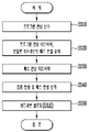
도 5는 본 발명의 일 실시 예에 따른 반도체 메모리 장치의 동작을 설명하기 위한 순서도이다.5 is a flowchart illustrating an operation of a semiconductor memory device according to an embodiment of the present invention.
도 6은 본 발명의 일 실시 예에 따른 반도체 메모리 장치의 동작시 메모리 셀 어레이에 인가되는 신호들의 파형도이다.6 is a waveform diagram of signals applied to a memory cell array during operation of a semiconductor memory device according to an embodiment of the present invention.
도 7a 내지 도 7d는 본 발명의 일 실시 예에 따른 반도체 메모리 장치의 프로그램 동작시 메모리 셀의 메모리막에 트랩된 전하들의 움직임을 설명하기 위한 구성도이다.7A to 7D are diagrams illustrating the movement of charges trapped in a memory layer of a memory cell during a program operation of a semiconductor memory device according to an embodiment of the present invention.
도 1 내지 도 7d를 참조하여, 본 발명의 일 실시 예에 따른 반도체 메모리 장치의 동작 방법을 설명하면 다음과 같다.A method of operating a semiconductor memory device according to an embodiment of the present invention will be described with reference to FIGS. 1 to 7D .
1) 프로그램 전압 인가(S110; A 구간)1) Program voltage application (S110; section A)
반도체 메모리 장치의 프로그램 동작을 위한 커맨드(CMD)가 제어 로직(140)으로 수신되면, 제어 로직(140)은 제어 신호들(PB_signals)을 출력한다. 읽기 및 쓰기 회로(130)는 제어 로직(140)에서 출력되는 제어 신호들(PB_signals)에 응답하여 외부로부터 입력되는 프로그램할 데이터(DATA)를 다수의 페이지 버퍼들(PB1~PBm)에 임시 저장한다. 다수의 페이지 버퍼들(PB1~PBm) 각각은 프로그램 동작시 입력된 데이터(DATA)를 임시 저장하고, 임시 저장된 데이터에 따라 각각 대응하는 비트 라인들(BL1 내지 BLm)의 전위를 제어한다.When a command CMD for a program operation of the semiconductor memory device is received by the
전압 생성부(150)는 제어 로직(140)에서 출력되는 제어 신호들(VG_signals)에 응답하여 프로그램 전압(Vpgm) 및 제1 패스 전압(Vpass1)을 생성한다. 어드레스 디코더(120)는 제어 로직(140)에서 출력되는 제어 신호들(AD_signals) 및 어드레스(ADDR)에 응답하여 다수의 워드라인들(WLs) 중 선택된 워드라인(예를 들어 WL1)에 프로그램 전압(Vpgm)을 인가하고, 나머지 비 선택된 워드라인들(예를 들어 WL0, WL2)에 제1 패스 전압(Vpass1)을 인가한다.The
이로 인하여 도 7a와 같이 선택된 워드라인(WL1)과 연결된 선택된 메모리 셀의 메모리막(ML)에 수직 채널층(SP)으로 부터 전하(ⓔ)들이 유입되어 트랩된다. 이로 인하여 선택된 메모리 셀의 문턱 전압이 상승한다.Accordingly, as shown in FIG. 7A , charges ⓔ flow from the vertical channel layer SP into the memory layer ML of the selected memory cell connected to the selected word line WL1 and are trapped. As a result, the threshold voltage of the selected memory cell increases.
2) 프로그램 전압 디스차지, 인접한 워드라인의 패스 전압 유지(S120; B 구간)2) Discharging the program voltage, maintaining the pass voltage of the adjacent word line (S120; section B)
A 구간 이후, 전압 생성부(150)는 선택된 워드라인(예를 들어 WL1)에 인가되던 프로그램 전압(Vpgm)의 전위 레벨을 0V의 전압으로 디스차지시킨다. 전압 생성부(150)는 선택된 워드라인(예를 들어 WL1)과 인접한 워드라인들(WL0, 및 WL1)에 제1 패스 전압(Vpass1)을 계속적으로 인가하거나, 제1 패스 전압(Vpass1)보다 전위 레벨이 높은 제2 패스 전압(Vpass2)을 인가한다.After section A, the
이로 인하여 도 7b와 같이 선택된 워드라인(WL1)과 인접한 워드라인들(WL0 및 WL2)에 인가되는 제1 패스 전압(Vpass1) 또는 제2 패스 전압(Vpass2)에 의해 전계가 생성되어 선택된 메모리 셀의 메모리막(ML)에 트랩된 전하(ⓔ)들 중 일부가 사이드 방향으로 이동하게 된다. 즉, 선택된 메모리 셀과 인접한 메모리 셀들 사이의 메모리막(ML)으로 전하(ⓔ)들 중 일부가 이동하게된다.For this reason, as shown in FIG. 7B , an electric field is generated by the first pass voltage Vpass1 or the second pass voltage Vpass2 applied to the word lines WL0 and WL2 adjacent to the selected word line WL1, so that the selected memory cell Some of the charges ⓔ trapped in the memory layer ML move in the side direction. That is, some of the charges ⓔ move to the memory layer ML between the selected memory cell and adjacent memory cells.
3) 패스 전압 디스차지(S130; C 구간)3) Pass voltage discharge (S130; section C)
B 구간 이후, 전압 생성부(150)는 인접한 워드라인들(WL0, 및 WL1)에 인가되던 제1 패스 전압(Vpass1) 또는 제2 패스 전압(Vpass2)의 전위 레벨을 0V의 전압으로 디스차지시킨다.After section B, the
이로 인하여 도 7c와 같이 선택된 메모리 셀과 인접한 메모리 셀들 사이의 메모리막(ML)으로 이동한 전하(ⓔ)들 및 선택된 메모리 셀의 메모리막(ML)에 트랩된 전하(ⓔ)들은 재배열 상태가 된다. 따라서, 전하들이 메모리막(ML)에 트랩된 후 짧은 시간 내에 인접 영역으로 이동하여 문턱 전압이 하강하는 숏 타임(short time) 리텐션 특성이 선택된 메모리 셀의 문턱 전압에 반영된 상태가 된다.Accordingly, as shown in FIG. 7C , the charges ⓔ moved to the memory layer ML between the selected memory cell and adjacent memory cells and the charges ⓔ trapped in the memory layer ML of the selected memory cell are rearranged. do. Accordingly, after the charges are trapped in the memory layer ML, they move to an adjacent region within a short time, and a short time retention characteristic in which the threshold voltage falls is reflected in the threshold voltage of the selected memory cell.
4) 검증 전압 및 패스 전압 인가(S140; D 구간)4) Verification voltage and pass voltage application (S140; D section)
C 구간 이후, 전압 생성부(150)는 제어 로직(140)에서 출력되는 제어 신호들(VG_signals)에 응답하여 검증 전압(Vverify) 및 제3 패스 전압(Vpass3)을 생성한다. 어드레스 디코더(120)는 제어 로직(140)에서 출력되는 제어 신호들(AD_signals) 및 어드레스(ADDR)에 응답하여 다수의 워드라인들(WLs) 중 선택된 워드라인(예를 들어 WL1)에 검증 전압(Vverify)을 인가하고, 나머지 비 선택된 워드라인들(예를 들어 WL0, WL2)에 제3 패스 전압(Vpass3)을 인가한다.After section C, the
읽기 및 쓰기 회로(130)의 다수의 페이지 버퍼들(PB1~PBm) 각각은 제어 로직(140)에서 출력되는 제어 신호들(PB_signals)에 응답하여 대응하는 비트 라인들(BL1 내지 BLm)의 전위 레벨 또는 전류량을 센싱하여 검증 동작을 수행한다.Each of the plurality of page buffers PB1 to PBm of the read and write
5) 워드라인 플로팅(S150; E 구간)5) Floating word line (S150; section E)
D 구간 이후, 전압 생성부(150)는 선택된 워드라인(예를 들어 WL1)에 인가되는 검증 전압(Vverify) 및 제3 전압(Vpass3)을 0V의 전압으로 디스차지하고, 어드레스 디코더(120)는 워드라인들(WLs)을 플로팅시켜 아이들(Idle) 상태가 되도록 한다.After the period D, the
상술한 워드라인 플로팅 단계(S150) 이 후, 검증 동작 결과 페일로 판단될 경우 프로그램 전압(Vpgm)을 스텝 전압만큼 상승시켜 상술한 프로그램 전압 인가 단계(S110)부터 재수행하고, 검증 동작 결과 패스로 판단될 경우 다음 페이지의 메모리 셀들에 대한 프로그램 동작을 수행할 수 있다.After the above-described word line floating step (S150), if it is determined that the verification operation fails, the program voltage Vpgm is increased by the step voltage and the above-described program voltage application step S110 is performed again, and the verification operation result is determined as a pass. In this case, a program operation may be performed on the memory cells of the next page.
상술한 본원 발명의 일 실시 예에 따르면, 프로그램 전압을 인가한 후 트랩된 전하들을 선택된 메모리 셀의 사이드 방향으로 이동시켜 재배열시킨 후 숏 타임 리텐션 특성이 반영된 후 검증 동작을 수행함으로써 검증 동작 이후 문턱 전압 분포가 하강하는 문제점을 개선할 수 있다.According to the above-described embodiment of the present invention, after applying the program voltage, the trapped charges are moved in the side direction of the selected memory cell to rearrange them, and after the short time retention characteristic is reflected, the verification operation is performed to perform the verification operation. A problem in which the threshold voltage distribution falls may be improved.
도 8은 본 발명의 다른 실시 예에 따른 반도체 메모리 장치의 동작을 설명하기 위한 순서도이다.8 is a flowchart illustrating an operation of a semiconductor memory device according to another embodiment of the present invention.
도 9는 본 발명의 다른 실시 예에 따른 반도체 메모리 장치의 동작시 메모리 셀 어레이에 인가되는 신호들의 파형도이다.9 is a waveform diagram of signals applied to a memory cell array during operation of a semiconductor memory device according to another embodiment of the present invention.
도 10a 내지 10d는 본 발명의 다른 실시 예에 따른 반도체 메모리 장치의 프로그램 동작시 메모리 셀의 메모리막에 트랩된 전하들의 움직임을 설명하기 위한 구성도이다.10A to 10D are block diagrams for explaining the movement of charges trapped in a memory layer of a memory cell during a program operation of a semiconductor memory device according to another embodiment of the present invention.
도 1 내지 도 4 및 도 8 내지 도 10d를 참조하여, 본 발명의 다른 실시 예에 따른 반도체 메모리 장치의 동작 방법을 설명하면 다음과 같다.An operating method of a semiconductor memory device according to another exemplary embodiment of the present invention will be described with reference to FIGS. 1 to 4 and 8 to 10D .
1) 프로그램 전압 인가(S210; A 구간)1) Program voltage application (S210; section A)
반도체 메모리 장치의 프로그램 동작을 위한 커맨드(CMD)가 제어 로직(140)으로 수신되면, 제어 로직(140)은 제어 신호들(PB_signals)을 출력한다. 읽기 및 쓰기 회로(130)는 제어 로직(140)에서 출력되는 제어 신호들(PB_signals)에 응답하여 외부로부터 입력되는 프로그램할 데이터(DATA)를 다수의 페이지 버퍼들(PB1~PBm)에 임시 저장한다. 다수의 페이지 버퍼들(PB1~PBm) 각각은 프로그램 동작시 입력된 데이터(DATA)를 임시 저장하고, 임시 저장된 데이터에 따라 각각 대응하는 비트 라인들(BL1 내지 BLm)의 전위를 제어한다.When a command CMD for a program operation of the semiconductor memory device is received by the
전압 생성부(150)는 제어 로직(140)에서 출력되는 제어 신호들(VG_signals)에 응답하여 프로그램 전압(Vpgm), 제1 패스 전압(Vpass1), 및 드레인 제어 전압(VDSL)을 생성한다. 어드레스 디코더(120)는 제어 로직(140)에서 출력되는 제어 신호들(AD_signals) 및 어드레스(ADDR)에 응답하여 다수의 워드라인들(WLs) 중 선택된 워드라인(예를 들어 WL1)에 프로그램 전압(Vpgm)을 인가하고, 나머지 비 선택된 워드라인들(예를 들어 WL0, WL2)에 제1 패스 전압(Vpass1)을 인가하고, 드레인 선택 라인(DSL)에 드레인 제어 전압(VDSL)을 인가한다.The
이로 인하여 도 10a와 같이 선택된 워드라인(WL1)과 연결된 선택된 메모리 셀의 메모리막(ML)에 수직 채널층(SP)으로 부터 전하(ⓔ)들이 유입되어 트랩된다. 이로 인하여 선택된 메모리 셀의 문턱 전압이 상승한다.Accordingly, as shown in FIG. 10A , charges ⓔ flow from the vertical channel layer SP into the memory layer ML of the selected memory cell connected to the selected word line WL1 and are trapped. As a result, the threshold voltage of the selected memory cell increases.
2) 프로그램 전압과 드레인 제어전압 디스차지, 인접한 워드라인의 패스 전압 유지(S220; B 구간)2) Discharging the program voltage and the drain control voltage, and maintaining the pass voltage of the adjacent word line (S220; section B)
A 구간 이후, 전압 생성부(150)는 선택된 워드라인(예를 들어 WL1)에 인가되던 프로그램 전압(Vpgm)의 전위 레벨을 0V의 전압으로 디스차지시킨다. 전압 생성부(150)는 선택된 워드라인(예를 들어 WL1)과 인접한 워드라인들(WL0, 및 WL1)에 제1 패스 전압(Vpass1)을 계속적으로 인가하거나, 제1 패스 전압(Vpass1)보다 전위 레벨이 높은 제2 패스 전압(Vpass2)을 인가한다. 전압 생성부(150)는 드레인 선택 라인(DSL)에 인가되는 드레인 제어 전압(VDSL)의 전위 레벨을 0V의 전압으로 디스차지시킨다. 이로 인하여 드레인 선택 트랜지스터(DST)는 턴오프되어 메모리 스트링의 채널(SP)은 대응하는 비트 라인과 전기적으로 분리되어 플로팅 상태가 된다. 이때 소스 선택 트랜지스터(SST)는 턴오프 상태이다. 따라서 제1 패스 전압(Vpass1) 또는 제2 패스 전압(Vpass2)이 인가되는 인접한 메모리 셀들의 채널은 높은 전위 레벨로 부스팅(High Boosting)되고, 0V의 전압이 인가되는 선택된 메모리 셀은 상대적으로 낮은 전위 레벨로 부스팅(Low Boosting)된다.After section A, the
이로 인하여 도 10b와 같이 선택된 워드라인(WL1)과 인접한 워드라인들(WL0 및 WL2)에 인가되는 제1 패스 전압(Vpass1) 또는 제2 패스 전압(Vpass2) 및 인접한 채널의 부스팅 전위에 의해 전계가 생성되어 선택된 메모리 셀의 메모리막(ML)에 트랩된 전하(ⓔ)들 중 일부가 사이드 방향으로 이동하게 된다. 즉, 선택된 메모리 셀과 인접한 메모리 셀들 사이의 메모리막(ML)으로 전하(ⓔ)들 중 일부가 이동하게된다.For this reason, as shown in FIG. 10B , an electric field is generated by the first pass voltage Vpass1 or the second pass voltage Vpass2 applied to the word lines WL0 and WL2 adjacent to the selected word line WL1 and the boosting potential of the adjacent channel. Some of the generated and trapped charges ⓔ in the memory layer ML of the selected memory cell move in the side direction. That is, some of the charges ⓔ move to the memory layer ML between the selected memory cell and adjacent memory cells.
3) 패스 전압 디스차지(S230; C 구간)3) Pass voltage discharge (S230; section C)
B 구간 이후, 전압 생성부(150)는 인접한 워드라인들(WL0, 및 WL1)에 인가되던 제1 패스 전압(Vpass1) 또는 제2 패스 전압(Vpass2)의 전위 레벨을 0V의 전압으로 디스차지시킨다.After section B, the
이로 인하여 도 10c와 같이 선택된 메모리 셀과 인접한 메모리 셀들 사이의 메모리막(ML)으로 이동한 전하(ⓔ)들 및 선택된 메모리 셀의 메모리막(ML)에 트랩된 전하(ⓔ)들은 재배열 상태가 된다. 따라서 숏 타임 리텐션 특성이 선택된 메모리 셀의 문턱 전압에 반영된 상태가 된다.Accordingly, as shown in FIG. 10C , the charges ⓔ moved to the memory layer ML between the selected memory cell and adjacent memory cells and the charges ⓔ trapped in the memory layer ML of the selected memory cell are rearranged. do. Accordingly, the short-time retention characteristic is reflected in the threshold voltage of the selected memory cell.
4) 검증 전압 및 패스 전압 인가(S240; D 구간)4) Applying verification voltage and pass voltage (S240; D section)
C 구간 이후, 전압 생성부(150)는 제어 로직(140)에서 출력되는 제어 신호들(VG_signals)에 응답하여 검증 전압(Vverify), 제3 패스 전압(Vpass3), 및 드레인 제어 전압(VDSL)을 생성한다. 어드레스 디코더(120)는 제어 로직(140)에서 출력되는 제어 신호들(AD_signals) 및 어드레스(ADDR)에 응답하여 다수의 워드라인들(WLs) 중 선택된 워드라인(예를 들어 WL1)에 검증 전압(Vverify)을 인가하고, 나머지 비 선택된 워드라인들(예를 들어 WL0, WL2)에 제3 패스 전압(Vpass3)을 인가하고, 드레인 선택 라인(DSL)에 드레인 제어 전압(VDSL)을 인가한다.After section C, the
읽기 및 쓰기 회로(130)의 다수의 페이지 버퍼들(PB1~PBm) 각각은 제어 로직(140)에서 출력되는 제어 신호들(PB_signals)에 응답하여 대응하는 비트 라인들(BL1 내지 BLm)의 전위 레벨 또는 전류량을 센싱하여 검증 동작을 수행한다.Each of the plurality of page buffers PB1 to PBm of the read and write
5) 워드라인 플로팅(S250)5) Floating word line (S250)
D 구간 이후, 전압 생성부(150)는 선택된 워드라인(예를 들어 WL1)에 인가되는 검증 전압(Vverify), 제3 전압(Vpass3), 드레인 제어 전압(VDSL)을 0V의 전압으로 디스차지하고, 어드레스 디코더(120)는 워드라인들(WLs)을 플로팅시켜 아이들(Idle) 상태가 되도록 한다.After the D period, the
상술한 워드라인 플로팅 단계(S150) 이 후, 검증 동작 결과 페일로 판단될 경우 프로그램 전압(Vpgm)을 스텝 전압만큼 상승시켜 상술한 프로그램 전압 인가 단계(S210)부터 재수행하고, 검증 동작 결과 패스로 판단될 경우 다음 페이지의 메모리 셀들에 대한 프로그램 동작을 수행할 수 있다.After the word line floating step S150 described above, if it is determined that the verification operation fails as a result of the verification operation, the program voltage Vpgm is increased by the step voltage and the above-described program voltage application step S210 is performed again, and the verification operation result is determined as a pass In this case, a program operation may be performed on the memory cells of the next page.
상술한 본원 발명의 일 실시 예에 따르면, 프로그램 전압을 인가한 후 트랩된 전하들을 선택된 메모리 셀의 사이드 방향으로 이동시켜 재배열시킨 후 숏 타임 리텐션 특성이 반영된 후 검증 동작을 수행함으로써 검증 동작 이후 문턱 전압 분포가 하강하는 문제점을 개선할 수 있다.According to the above-described embodiment of the present invention, after applying the program voltage, the trapped charges are moved in the side direction of the selected memory cell to rearrange them, and after the short time retention characteristic is reflected, the verification operation is performed to perform the verification operation. A problem in which the threshold voltage distribution falls may be improved.
도 11은 본 발명의 또 다른 실시 예에 따른 반도체 메모리 장치의 동작을 설명하기 위한 순서도이다.11 is a flowchart for explaining an operation of a semiconductor memory device according to another embodiment of the present invention.
도 12a 및 도 12b는 본 발명의 또 다른 실시 예에 따른 반도체 메모리 장치의 동작시 메모리 셀 어레이에 인가되는 신호들의 파형도이다.12A and 12B are waveform diagrams of signals applied to a memory cell array during operation of a semiconductor memory device according to still another exemplary embodiment of the present invention.
도 13a 내지 도 13d는 본 발명의 또 다른 실시 예에 따른 반도체 메모리 장치의 동작시 메모리 셀의 메모리막에 트랩된 전하들의 움직임을 설명하기 위한 구성도이다.13A to 13D are diagrams illustrating the movement of charges trapped in a memory layer of a memory cell during operation of a semiconductor memory device according to another exemplary embodiment of the present invention.
도 1 내지 도 4 및 도 11 내지 도 13d를 참조하여, 본 발명의 또 다른 실시 예에 따른 반도체 메모리 장치의 동작 방법을 설명하면 다음과 같다.An operating method of a semiconductor memory device according to another exemplary embodiment of the present invention will be described with reference to FIGS. 1 to 4 and 11 to 13D .
본 발명의 또 다른 실시 예에 따른 반도체 메모리 장치의 동작 방법은 프로그램 동작 이전에 수행하는 것이 바람직하다.The method of operating a semiconductor memory device according to another embodiment of the present invention is preferably performed before a program operation.
1) 이븐 워드라인들에 프로그램 전압 인가, 오드 워드라인들에 패스 전압 인가(S310)1) A program voltage is applied to the even word lines and a pass voltage is applied to the odd word lines (S310)
읽기 및 쓰기 회로(130)는 제어 로직(140)에서 출력되는 제어 신호들(PB_signals)에 응답하여 메모리 셀 어레이(110)의 다수의 비트 라인들(BL1 내지 BLm)의 전위를 프로그램 허용 레벨(예를 들어 0V)로 설정한다.The read and write
전압 생성부(150)는 제어 로직(140)에서 출력되는 제어 신호들(VG_signals)에 응답하여 프로그램 전압(Vpgm), 제1 패스 전압(Vpass1) 및 드레인 제어 전압(VDSL)을 생성한다. 어드레스 디코더(120)는 제어 로직(140)에서 출력되는 제어 신호들(AD_signals) 및 어드레스(ADDR)에 응답하여 다수의 워드라인들(WLs) 중 이븐 워드라인들(WL0, WL2, ...)에 프로그램 전압(Vpgm)을 인가하고, 오드 워드라인들(WL1, WL3, ...)에 제1 패스 전압(Vpass1)을 인가하고, 드레인 선택 라인(DSL)에 드레인 제어 전압(VDSL)을 인가한다.The
이로 인하여 도 13a와 같이 이븐 워드라인들(WL0, WL2, ...)과 연결된 이븐 메모리 셀들의 메모리막(ML)에 수직 채널층(SP)으로 부터 전하(ⓔ)들이 유입되어 트랩된다. 따라서 이븐 메모리 셀들의 문턱 전압이 상승한다.Accordingly, as shown in FIG. 13A , electric charges ⓔ are introduced from the vertical channel layer SP into the memory film ML of the even memory cells connected to the even word lines WL0, WL2, ... and are trapped. Accordingly, the threshold voltages of the even memory cells increase.
2) 이븐 워드라인들 디스차지, 오드 워드라인들에 프로그램 전압 인가(S320)2) Even word lines are discharged, and a program voltage is applied to odd word lines (S320)
전압 생성부(150)는 제어 로직(140)에서 출력되는 제어 신호들(VG_signals)에 응답하여 이븐 워드라인들(WL0, WL2, ...)에 인가되던 프로그램 전압(Vpgm)을 0V의 전압으로 디스차지하고, 제1 패스 전압(Vpass1)이 인가되던 오드 워드라인들(WL1, WL3, ...)에 프로그램 전압(Vpgm)을 인가한다. 전압 생성부(150)는 드레인 선택 라인(DSL)에 인가되던 드레인 제어 전압(VDSL)을 0V로 디스차지한다. 이로 인하여 드레인 선택 트랜지스터(DST)는 턴오프되어 메모리 스트링의 채널(SP)은 대응하는 비트 라인과 전기적으로 분리되어 플로팅 상태가 된다. 이때 소스 선택 트랜지스터(SST)는 턴오프 상태이다. The
이로 인하여 도 13b와 같이 프로그램 전압(Vpgm) 인가되는 오드 워드라인들과 연결된 오드 메모리 셀들의 채널은 높은 전위 레벨로 부스팅(High Boosting)되고, 0V의 전압이 인가되는 이븐 메모리 셀들은 상대적으로 낮은 전위 레벨로 부스팅(Low Boosting)된다. 따라서 프로그램 전압(Vpgm) 및 인접한 채널의 부스팅 전위에 의해 전계가 생성되어 이븐 메모리 셀들의 메모리막(ML)에 트랩된 전하(ⓔ)들 중 일부가 양 사이드 방향으로 이동하게 된다.Accordingly, as shown in FIG. 13B , channels of odd memory cells connected to odd word lines to which a program voltage Vpgm are applied are boosted to a high potential level, and even memory cells to which a voltage of 0V is applied have a relatively low potential. Level is boosted (Low Boosting). Accordingly, an electric field is generated by the program voltage Vpgm and the boosting potential of an adjacent channel, and some of the charges ⓔ trapped in the memory layer ML of the even memory cells move in both side directions.
3) 소거 동작(S330)3) Erase operation (S330)
S320 단계 이 후, 소거 동작을 수행하여 이븐 메모리 셀들의 메모리막(ML)에 트랩된 전하(ⓔ)들을 디트랩시킨다. 소거 동작시 이븐 메모리 셀들의 양 사이드 방향으로 이동한 전하(ⓔ)들은 잔류되도록 수행한다. 소거 동작은 메모리 셀 어레이(110)의 소스 라인(SL)에 전압 생성부(150)에서 생성된 소거 전압을 인가하여 수행할 수 있다.After step S320, an erase operation is performed to detrap the charges ⓔ trapped in the memory layer ML of the even memory cells. During the erase operation, charges (ⓔ) that have moved to both sides of the even memory cells remain. The erase operation may be performed by applying the erase voltage generated by the
소거 동작(S330)은 스킵(skip)하고 다음 단계(S340)를 수행할 수 있다.The erase operation ( S330 ) may be skipped and the next step ( S340 ) may be performed.
4) 오드 워드라인들에 프로그램 전압 인가, 이븐 워드라인들에 패스 전압 인가(S340)4) A program voltage is applied to the odd word lines and a pass voltage is applied to the even word lines (S340)
전압 생성부(150)는 제어 로직(140)에서 출력되는 제어 신호들(VG_signals)에 응답하여 프로그램 전압(Vpgm), 제1 패스 전압(Vpass1), 및 드레인 제어 전압(VDSL)을 생성한다. 어드레스 디코더(120)는 제어 로직(140)에서 출력되는 제어 신호들(AD_signals) 및 어드레스(ADDR)에 응답하여 다수의 워드라인들(WLs) 중 오드 워드라인들(WL1, WL3, ...)에 프로그램 전압(Vpgm)을 인가하고, 이븐 워드라인들(WL0, WL2, ...)에 제1 패스 전압(Vpass1)을 인가하고, 드레인 선택 라인(DSL)에 드레인 제어 전압(VDSL)을 인가한다.The
이로 인하여 도 13c와 같이 오드 워드라인들(WL1, WL3, ...)과 연결된 오드 메모리 셀들의 메모리막(ML)에 수직 채널층(SP)으로 부터 전하(ⓔ)들이 유입되어 트랩된다. 따라서 오드 메모리 셀들의 문턱 전압이 상승한다. 또한 이븐 메모리 셀들의 양 사이드에는 S320 단계에서 이동한 전하들(A)이 잔류한다.Accordingly, as shown in FIG. 13C , charges ⓔ are introduced from the vertical channel layer SP into the memory film ML of the odd memory cells connected to the odd word lines WL1, WL3, ... and are trapped. Accordingly, the threshold voltages of the odd memory cells increase. In addition, the charges A moved in step S320 remain on both sides of the even memory cells.
5) 오드 워드라인들 디스차지, 이븐 워드라인들에 프로그램 전압 인가(S350)5) Discharging the odd word lines and applying a program voltage to the even word lines (S350)
전압 생성부(150)는 제어 로직(140)에서 출력되는 제어 신호들(VG_signals)에 응답하여 오드 워드라인들(WL1, WL3, ...)에 인가되던 프로그램 전압(Vpgm)을 0V의 전압으로 디스차지하고, 제1 패스 전압(Vpass1)이 인가되던 이븐 워드라인들(WL0, WL2, ...)에 프로그램 전압(Vpgm)을 인가한다.The
전압 생성부(150)는 드레인 선택 라인(DSL)에 인가되던 드레인 제어 전압(VDSL)을 0V로 디스차지한다. 이로 인하여 드레인 선택 트랜지스터(DST)는 턴오프되어 메모리 스트링의 채널(SP)은 대응하는 비트 라인과 전기적으로 분리되어 플로팅 상태가 된다. 이때 소스 선택 트랜지스터(SST)는 턴오프 상태이다. The
이로 인하여 도 13d와 같이 프로그램 전압(Vpgm) 인가되는 이븐 워드라인들과 연결된 이븐 메모리 셀들의 채널은 높은 전위 레벨로 부스팅(High Boosting)되고, 0V의 전압이 인가되는 오드 메모리 셀들은 상대적으로 낮은 전위 레벨로 부스팅(Low Boosting)된다. 따라서 프로그램 전압(Vpgm) 및 인접한 채널의 부스팅 전위에 의해 전계가 생성되어 오드 메모리 셀들의 메모리막(ML)에 트랩된 전하(ⓔ)들 중 일부가 양 사이드 방향으로 이동하게 된다.Accordingly, as shown in FIG. 13D , the channels of the even memory cells connected to the even word lines to which the program voltage Vpgm is applied are boosted to a high potential level, and the odd memory cells to which the voltage of 0V is applied have a relatively low potential. Level is boosted (Low Boosting). Accordingly, an electric field is generated by the program voltage Vpgm and the boosting potential of an adjacent channel, and some of the charges ⓔ trapped in the memory layer ML of the odd memory cells move in both side directions.
6) 소거 동작(S360)6) Erase operation (S360)
S350 단계 이 후 소거 동작을 수행하여, 오드 메모리 셀들의 메모리막(ML)에 트랩된 전하(ⓔ)들을 디트랩시킨다. 소거 동작은 메모리 셀 어레이(110)의 소스 라인(SL)에 전압 생성부(150)에서 생성된 소거 전압을 인가하여 수행할 수 있다. 만약 상술한 소거 동작(S330)을 스킵하였다면, 소거 동작(S360) 단계에서 이븐 메모리 셀들 및 오드 메모리 셀들의 소거 동작이 함께 수행된다. 소거 동작시 메모리 셀들의 양 사이드 방향으로 이동한 전하들(A,B)은 잔류되도록 수행하는 것이 바람직하다.After step S350, an erase operation is performed to detrap the charges ⓔ trapped in the memory layer ML of the odd memory cells. The erase operation may be performed by applying the erase voltage generated by the
이 후, 프로그램 동작을 수행할 수 있다.After that, a program operation may be performed.
상술한 바와 같이 본원 발명의 실시 예에 따르면, 프로그램 동작 이전에 메모리 셀들 사이의 메모리막 내에 전하들을 미리 트랩시켜 전하 밀도를 높여 놓을 수 있다. 따라서 후속 프로그램 동작시 메모리 셀들의 메모리막에 트랩된 전하들이 양 사이드로 이동하는 현상을 억제하여 문턱 전압이 변화하는 문제점을 개선할 수 있다.As described above, according to the exemplary embodiment of the present invention, charges may be pre-trapped in the memory layer between the memory cells prior to the program operation to increase the charge density. Accordingly, it is possible to suppress a phenomenon in which charges trapped in the memory layer of the memory cells move to both sides during a subsequent program operation, thereby improving the problem of a change in the threshold voltage.
도 14는 본 발명의 또 다른 실시 예에 따른 반도체 메모리 장치의 동작을 설명하기 위한 순서도이다.14 is a flowchart for explaining an operation of a semiconductor memory device according to another embodiment of the present invention.
도 15는 본 발명의 또 다른 실시 예에 따른 반도체 메모리 장치의 동작시 메모리 셀 어레이에 인가되는 신호들의 파형도이다.15 is a waveform diagram of signals applied to a memory cell array during operation of a semiconductor memory device according to another embodiment of the present invention.
도 16a 내지 도 16d는 본 발명의 또 다른 실시 예에 따른 반도체 메모리 장치의 동작시 메모리 셀의 메모리막에 트랩된 전하들의 움직임을 설명하기 위한 구성도이다.16A to 16D are diagrams for explaining the movement of charges trapped in a memory layer of a memory cell during operation of a semiconductor memory device according to another embodiment of the present invention.
도 1 내지 도 4 및 도 14 내지 도 16d를 참조하여, 본 발명의 또 다른 실시 예에 따른 반도체 메모리 장치의 동작 방법을 설명하면 다음과 같다.An operating method of a semiconductor memory device according to another exemplary embodiment of the present invention will be described with reference to FIGS. 1 to 4 and 14 to 16D .
본 발명의 또 다른 실시 예에 따른 반도체 메모리 장치의 동작 방법은 반도체 메모리 장치의 소거 동작에 포함될 수 있으며, 좀 더 상세하게는 반도체 메모리 장치의 소거 동작 중 소거 전압 인가 동작 이전에 수행하는 것이 바람직하다.The method of operating a semiconductor memory device according to another embodiment of the present invention may be included in an erase operation of the semiconductor memory device, and in more detail, it is preferable to perform it before an erase voltage application operation during an erase operation of the semiconductor memory device. .
또한 본 발명의 또 다른 실시 예에 따른 반도체 메모리 장치의 동작 방법 프로그램 동작 이전에 수행될 수도 있다. Also, the method of operating a semiconductor memory device according to another embodiment of the present invention may be performed before the program operation.
1) 모든 워드라인들에 프로그램 전압 인가(S410)1) A program voltage is applied to all word lines (S410)
읽기 및 쓰기 회로(130)는 제어 로직(140)에서 출력되는 제어 신호들(PB_signals)에 응답하여 메모리 셀 어레이(110)의 다수의 비트 라인들(BL1 내지 BLm)의 전위를 프로그램 허용 레벨(예를 들어 0V)로 설정한다.The read and write
전압 생성부(150)는 제어 로직(140)에서 출력되는 제어 신호들(VG_signals)에 응답하여 프로그램 전압(Vpgm) 및 드레인 제어 전압(VDSL)을 생성한다. 어드레스 디코더(120)는 제어 로직(140)에서 출력되는 제어 신호들(AD_signals)에 응답하여 다수의 워드라인들(WLs)에 프로그램 전압(Vpgm)을 인가하고, 드레인 선택 라인(DSL)에 드레인 제어 전압(VDSL)을 인가한다.The
이로 인하여 도 16a와 같이 모든 워드라인들(WLs; WL0, WL1, WL2, WL3, ...)과 연결된 모든 메모리 셀들의 메모리막(ML)에 수직 채널층(SP)으로 부터 전하(ⓔ)들이 유입되어 트랩된다. 이때 모든 워드라인들(WLs)에 인가되는 프로그램 전압(Vpgm)에 의해 메모리 셀들 사이의 메모리막(ML)에도 일부 전하(ⓔ)들이 트랩될 수 있다.As a result, as shown in FIG. 16A, charges (ⓔ) from the vertical channel layer SP in the memory film ML of all memory cells connected to all the word lines WLs; WL0, WL1, WL2, WL3, ...) inflow and trap. In this case, some charges ⓔ may be trapped in the memory layer ML between the memory cells by the program voltage Vpgm applied to all the word lines WLs.
2) 이븐 워드라인 디스차지, 드레인 제어 전압 디스차지(S420)2) Even word line discharge, drain control voltage discharge (S420)
전압 생성부(150)는 제어 로직(140)에서 출력되는 제어 신호들(VG_signals)에 응답하여 이븐 워드라인들(WL0, WL2,...)에 인가되던 프로그램 전압(Vpgm)의 전위 레벨을 디스차지한다. 예를 들어 이븐 워드라인들(WL0, WL2,...)에 인가되던 프로그램 전압(Vpgm)을 0V의 전압으로 디스차지할 수 있다. 전압 생성부(150)는 오드 워드라인들(WL1, WL3,...)에 인가되는 프로그램 전압(Vpgm)은 전위 레벨을 유지시킨다. 또한 전압 생성부(150)는 드레인 선택 라인(DSL)에 인가되던 드레인 제어 전압(VDSL)을 0V로 디스차지한다.The
이로 인하여 도 16b와 같이 프로그램 전압(Vpgm)이 인가되는 오드 워드라인들과 연결된 오드 메모리 셀들의 채널은 높은 전위 레벨로 부스팅(High Boosting)되고, 프로그램 전압(Vpgm)이 디스차지된 이븐 워드라인들과 연결된 이븐 메모리 셀들은 상대적으로 낮은 전위 레벨로 부스팅(Low Boosting)된다. 따라서 프로그램 전압(Vpgm) 및 인접한 채널의 부스팅 전위에 의해 전계가 생성되어 이븐 메모리 셀들의 메모리막(ML)에 트랩된 전하(ⓔ)들 중 일부가 양 사이드 방향으로 이동하게 된다.Accordingly, as shown in FIG. 16B , channels of odd memory cells connected to odd word lines to which program voltage Vpgm are applied are boosted to a high potential level, and even word lines to which program voltage Vpgm is discharged. Even memory cells connected to are boosted to a relatively low potential level (Low Boosting). Accordingly, an electric field is generated by the program voltage Vpgm and the boosting potential of an adjacent channel, and some of the charges ⓔ trapped in the memory layer ML of the even memory cells move in both side directions.
3) 이븐 워드라인에 프로그램 전압 인가, 오드 워드라인 디스차지(S430)3) Program voltage applied to even word line, odd word line discharge (S430)
전압 생성부(150)는 제어 로직(140)에서 출력되는 제어 신호들(VG_signals)에 응답하여 오드 워드라인들(WL1, WL3,...)에 인가되던 프로그램 전압(Vpgm)의 전위 레벨을 디스차지한다. 예를 들어 오드 워드라인들(WL1, WL3,...)에 인가되던 프로그램 전압(Vpgm)을 0V의 전압으로 디스차지할 수 있다. 전압 생성부(150)는 이븐 워드라인들(WL0, WL2, ...)에 프로그램 전압(Vpgm)을 인가한다.The
이로 인하여 도 16c와 같이 프로그램 전압(Vpgm) 인가되는 이븐 워드라인들과 연결된 이븐 메모리 셀들의 채널은 높은 전위 레벨로 부스팅(High Boosting)되고, 프로그램 전압(Vpgm)이 디스차지된 오드 워드라인들과 연결된 오드 메모리 셀들은 상대적으로 낮은 전위 레벨로 부스팅(Low Boosting)된다. 따라서 프로그램 전압(Vpgm) 및 인접한 채널의 부스팅 전위에 의해 전계가 생성되어 오드 메모리 셀들의 메모리막(ML)에 트랩된 전하(ⓔ)들 중 일부가 양 사이드 방향으로 이동하게 된다.For this reason, as shown in FIG. 16C , channels of even memory cells connected to the even word lines to which the program voltage Vpgm are applied are boosted to a high potential level, and the odd word lines to which the program voltage Vpgm is discharged. The connected odd memory cells are boosted to a relatively low potential level. Accordingly, an electric field is generated by the program voltage Vpgm and the boosting potential of an adjacent channel, and some of the charges ⓔ trapped in the memory layer ML of the odd memory cells move in both side directions.
4) 소거 동작(S440)4) Erase operation (S440)
소거 동작을 수행하여, 이븐 메모리 셀들 및 오드 메모리 셀들의 메모리막(ML)에 트랩된 전하(ⓔ)들을 디트랩시킨다. 소거 동작시 이븐 메모리 셀들과 오드 메모리 셀들 사이의 메모리막에 트랩된 전하(ⓔ)들은 잔류되도록 소거 동작을 수행한다. 소거 동작은 전압 생성부(150)에서 생성된 소거 전압이 메모리 셀 어레이(110)의 소스 라인에 인가되도록 하여 수행할 수 있다.The erase operation is performed to detrap the charges ⓔ trapped in the memory layer ML of the even memory cells and the odd memory cells. During the erase operation, the erase operation is performed so that charges (ⓔ) trapped in the memory layer between the even memory cells and the odd memory cells remain. The erase operation may be performed by applying the erase voltage generated by the
이 후, 프로그램 동작을 수행할 수 있다.After that, a program operation may be performed.
상술한 바와 같이 본원 발명의 실시 예에 따르면, 프로그램 동작 이전에 메모리 셀들 사이의 메모리막 내에 전하들을 미리 트랩시켜 전하 밀도를 높여 놓을 수 있다. 따라서 후속 프로그램 동작시 메모리 셀들의 메모리막에 트랩된 전하들이 양 사이드로 이동하는 현상을 억제하여 문턱 전압이 변화하는 문제점을 개선할 수 있다.As described above, according to the exemplary embodiment of the present invention, charges may be pre-trapped in the memory layer between the memory cells prior to the program operation to increase the charge density. Accordingly, it is possible to improve the problem that the threshold voltage changes by suppressing a phenomenon in which charges trapped in the memory layer of the memory cells move to both sides during a subsequent program operation.
도 17은 도 1의 반도체 메모리 장치를 포함하는 메모리 시스템을 보여주는 블럭도이다.17 is a block diagram illustrating a memory system including the semiconductor memory device of FIG. 1 .
도 17을 참조하면, 메모리 시스템(1000)은 반도체 메모리 장치(100) 및 컨트롤러(1100)를 포함한다.Referring to FIG. 17 , the
반도체 메모리 장치(100)는 도 1을 참조하여 설명된 바와 마찬가지로 구성되고, 동작할 수 있다. 이하, 중복되는 설명은 생략된다.The
컨트롤러(1100)는 호스트(Host) 및 반도체 메모리 장치(100)에 연결된다. 호스트(Host)로부터의 요청에 응답하여, 컨트롤러(1100)는 반도체 메모리 장치(100)를 액세스하도록 구성된다. 예를 들면, 컨트롤러(1100)는 반도체 메모리 장치(100)의 읽기, 쓰기, 소거, 그리고 배경(background) 동작을 제어하도록 구성된다. 컨트롤러(1100)는 반도체 메모리 장치(100) 및 호스트(Host) 사이에 인터페이스를 제공하도록 구성된다. 컨트롤러(1100)는 반도체 메모리 장치(100)를 제어하기 위한 펌웨어(firmware)를 구동하도록 구성된다.The
컨트롤러(1100)는 램(1110, Random Access Memory), 프로세싱 유닛(1120, processing unit), 호스트 인터페이스(1130, host interface), 메모리 인터페이스(1140, memory interface) 및 에러 정정 블록(1150)을 포함한다. 램(1110)은 프로세싱 유닛(1120)의 동작 메모리, 반도체 메모리 장치(100) 및 호스트(Host) 사이의 캐시 메모리, 그리고 반도체 메모리 장치(100) 및 호스트(Host) 사이의 버퍼 메모리 중 적어도 하나로서 이용된다. 프로세싱 유닛(1120)은 컨트롤러(1100)의 제반 동작을 제어한다. 또한 컨트롤러(1100)는 쓰기 동작시 호스트(Host)로 부터 제공되는 프로그램 데이터를 임시 저장할 수 있다.The
호스트 인터페이스(1130)는 호스트(Host) 및 컨트롤러(1100) 사이의 데이터 교환을 수행하기 위한 프로토콜을 포함한다. 예시적인 실시 예로서, 컨트롤러(1200)는 USB (Universal Serial Bus) 프로토콜, MMC (multimedia card) 프로토콜, PCI (peripheral component interconnection) 프로토콜, PCI-E (PCI-express) 프로토콜, ATA (Advanced Technology Attachment) 프로토콜, Serial-ATA 프로토콜, Parallel-ATA 프로토콜, SCSI (small computer small interface) 프로토콜, ESDI (enhanced small disk interface) 프로토콜, 그리고 IDE (Integrated Drive Electronics) 프로토콜, 사유(private) 프로토콜 등과 같은 다양한 인터페이스 프로토콜들 중 적어도 하나를 통해 호스트(Host)와 통신하도록 구성된다.The
메모리 인터페이스(1140)는 반도체 메모리 장치(100)와 인터페이싱한다. 예를 들면, 메모리 인터페이스는 낸드 인터페이스 또는 노어 인터페이스를 포함한다.The
에러 정정 블록(1150)은 에러 정정 코드(ECC, Error Correcting Code)를 이용하여 반도체 메모리 장치(100)로부터 수신된 데이터의 에러를 검출하고, 정정하도록 구성된다. 프로세싱 유닛(1120)은 에러 정정 블록(1150)의 에러 검출 결과에 따라 읽기 전압을 조절하고, 재 읽기를 수행하도록 반도체 메모리 장치(100)를 제어할 것이다. 예시적인 실시 예로서, 에러 정정 블록은 컨트롤러(1100)의 구성 요소로서 제공될 수 있다.The
컨트롤러(1100) 및 반도체 메모리 장치(100)는 하나의 반도체 장치로 집적될 수 있다. 예시적인 실시 예로서, 컨트롤러(1100) 및 반도체 메모리 장치(100)는 하나의 반도체 장치로 집적되어, 메모리 카드를 구성할 수 있다. 예를 들면, 컨트롤러(1100) 및 반도체 메모리 장치(100)는 하나의 반도체 장치로 집적되어 PC 카드(PCMCIA, personal computer memory card international association), 컴팩트 플래시 카드(CF), 스마트 미디어 카드(SM, SMC), 메모리 스틱, 멀티미디어 카드(MMC, RS-MMC, MMCmicro), SD 카드(SD, miniSD, microSD, SDHC), 유니버설 플래시 기억장치(UFS) 등과 같은 메모리 카드를 구성할 것이다.The
컨트롤러(1100) 및 반도체 메모리 장치(100)는 하나의 반도체 장치로 집적되어 반도체 드라이브(SSD, Solid State Drive)를 구성할 수 있다. 반도체 드라이브(SSD)는 반도체 메모리에 데이터를 저장하도록 구성되는 저장 장치를 포함한다. 메모리 시스템(1000)이 반도체 드라이브(SSD)로 이용되는 경우, 메모리 시스템(2000)에 연결된 호스트(Host)의 동작 속도는 획기적으로 개선된다.The
다른 예로서, 메모리 시스템(1000)은 컴퓨터, UMPC (Ultra Mobile PC), 워크스테이션, 넷북(net-book), PDA (Personal Digital Assistants), 포터블(portable) 컴퓨터, 웹 타블렛(web tablet), 무선 전화기(wireless phone), 모바일 폰(mobile phone), 스마트폰(smart phone), e-북(e-book), PMP(portable multimedia player), 휴대용 게임기, 네비게이션(navigation) 장치, 블랙박스(black box), 디지털 카메라(digital camera), 3차원 수상기(3-dimensional television), 디지털 음성 녹음기(digital audio recorder), 디지털 음성 재생기(digital audio player), 디지털 영상 녹화기(digital picture recorder), 디지털 영상 재생기(digital picture player), 디지털 동영상 녹화기(digital video recorder), 디지털 동영상 재생기(digital video player), 정보를 무선 환경에서 송수신할 수 있는 장치, 홈 네트워크를 구성하는 다양한 전자 장치들 중 하나, 컴퓨터 네트워크를 구성하는 다양한 전자 장치들 중 하나, 텔레매틱스 네트워크를 구성하는 다양한 전자 장치들 중 하나, RFID 장치, 또는 컴퓨팅 시스템을 구성하는 다양한 구성 요소들 중 하나 등과 같은 전자 장치의 다양한 구성 요소들 중 하나로 제공된다.As another example, the
예시적인 실시 예로서, 반도체 메모리 장치(100) 또는 메모리 시스템(1000)은 다양한 형태들의 패키지로 실장될 수 있다. 예를 들면, 반도체 메모리 장치(100) 또는 메모리 시스템(1000)은 PoP(Package on Package), Ball grid arrays(BGAs), Chip scale packages(CSPs), Plastic Leaded Chip Carrier(PLCC), Plastic Dual In Line Package(PDIP), Die in Waffle Pack, Die in Wafer Form, Chip On Board(COB), Ceramic Dual In Line Package(CERDIP), Plastic Metric Quad Flat Pack(MQFP), Thin Quad Flatpack(TQFP), Small Outline(SOIC), Shrink Small Outline Package(SSOP), Thin Small Outline(TSOP), Thin Quad Flatpack(TQFP), System In Package(SIP), Multi Chip Package(MCP), Wafer-level Fabricated Package(WFP), Wafer-Level Processed Stack Package(WSP) 등과 같은 방식으로 패키지화되어 실장될 수 있다.As an exemplary embodiment, the
도 18은 도 17의 메모리 시스템의 응용 예를 보여주는 블럭도이다.18 is a block diagram illustrating an application example of the memory system of FIG. 17 .
도 18을 참조하면, 메모리 시스템(2000)은 반도체 메모리 장치(2100) 및 컨트롤러(2200)를 포함한다. 반도체 메모리 장치(2100)는 복수의 반도체 메모리 칩들을 포함한다. 복수의 반도체 메모리 칩들은 복수의 그룹들로 분할된다.Referring to FIG. 18 , a
도 18에서, 복수의 그룹들은 각각 제 1 내지 제 k 채널들(CH1~CHk)을 통해 컨트롤러(2200)와 통신하는 것으로 도시되어 있다. 각 반도체 메모리 칩은 도 1을 참조하여 설명된 반도체 메모리 장치(100) 중 하나와 마찬가지로 구성되고, 동작할 것이다.In FIG. 18 , the plurality of groups are illustrated as communicating with the
각 그룹은 하나의 공통 채널을 통해 컨트롤러(2200)와 통신하도록 구성된다. 컨트롤러(2200)는 도 17을 참조하여 설명된 컨트롤러(1100)와 마찬가지로 구성되고, 복수의 채널들(CH1~CHk)을 통해 반도체 메모리 장치(2100)의 복수의 메모리 칩들을 제어하도록 구성된다.Each group is configured to communicate with the
도 19는 도 18을 참조하여 설명된 메모리 시스템을 포함하는 컴퓨팅 시스템을 보여주는 블럭도이다.19 is a block diagram illustrating a computing system including the memory system described with reference to FIG. 18 .
도 19를 참조하면, 컴퓨팅 시스템(3000)은 중앙 처리 장치(3100), 램(3200, RAM, Random Access Memory), 사용자 인터페이스(3300), 전원(3400), 시스템 버스(3500), 그리고 메모리 시스템(2000)을 포함한다.Referring to FIG. 19 , the
메모리 시스템(2000)은 시스템 버스(3500)를 통해, 중앙처리장치(3100), 램(3200), 사용자 인터페이스(3300), 그리고 전원(3400)에 전기적으로 연결된다. 사용자 인터페이스(3300)를 통해 제공되거나, 중앙 처리 장치(3100)에 의해서 처리된 데이터는 메모리 시스템(2000)에 저장된다.The
도 19에서, 반도체 메모리 장치(2100)는 컨트롤러(2200)를 통해 시스템 버스(3500)에 연결되는 것으로 도시되어 있다. 그러나, 반도체 메모리 장치(2100)는 시스템 버스(3500)에 직접 연결되도록 구성될 수 있다. 이때, 컨트롤러(2200)의 기능은 중앙 처리 장치(3100) 및 램(3200)에 의해 수행될 것이다.In FIG. 19 , the
도 19에서, 도 18을 참조하여 설명된 메모리 시스템(2000)이 제공되는 것으로 도시되어 있다. 그러나, 메모리 시스템(2000)은 도 17을 참조하여 설명된 메모리 시스템(1000)으로 대체될 수 있다. 예시적인 실시 예로서, 컴퓨팅 시스템(3000)은 도 17 및 도 18를 참조하여 설명된 메모리 시스템들(1000, 2000)을 모두 포함하도록 구성될 수 있다.In FIG. 19 , it is shown that the
본 발명의 상세한 설명에서는 구체적인 실시 예에 관하여 설명하였으나, 본 발명의 범위와 기술적 사상에서 벗어나지 않는 한도 내에서 다양한 변경이 가능하다. 그러므로 본 발명의 범위는 상술한 실시 예에 국한되어 정해져서는 안되며 후술하는 특허청구범위뿐만 아니라 이 발명의 특허청구범위와 균등한 것들에 의해 정해져야 한다.In the detailed description of the present invention, specific embodiments have been described, but various changes are possible without departing from the scope and technical spirit of the present invention. Therefore, the scope of the present invention should not be limited to the above-described embodiment, but should be defined by the following claims as well as the claims and equivalents of the present invention.
100: 반도체 메모리 장치 110: 메모리 셀 어레이
120: 어드레스 디코더 130: 읽기 및 쓰기 회로
140: 제어 로직 150 : 전압 생성부100: semiconductor memory device 110: memory cell array
120: address decoder 130: read and write circuit
140: control logic 150: voltage generator
Claims (18)
상기 메모리 셀 어레이에 프로그램 전압, 제1 및 제2 패스 전압, 및 드레인 제어 전압들을 인가하기 위한 전압 생성부; 및
프로그램 동작 시 상기 다수의 메모리 셀들 중 선택된 메모리 셀에 상기 프로그램 전압을 인가하고 상기 선택된 메모리 셀과 인접한 메모리 셀들에 상기 제1 패스 전압을 인가한 후, 상기 프로그램 전압을 접지 전압으로 디스차지 완료한 후 상기 인접한 메모리 셀들에 상기 제1 패스 전압보다 높은 상기 제2 패스 전압을 인가하도록 상기 전압 생성부를 제어하기 위한 제어 로직을 포함하는 반도체 메모리 장치.
a memory cell array including a drain select transistor and a plurality of memory cells;
a voltage generator for applying a program voltage, first and second pass voltages, and drain control voltages to the memory cell array; and
During a program operation, after applying the program voltage to a selected memory cell among the plurality of memory cells, applying the first pass voltage to memory cells adjacent to the selected memory cell, and after discharging the program voltage to a ground voltage, and a control logic for controlling the voltage generator to apply the second pass voltage higher than the first pass voltage to the adjacent memory cells.
상기 제어 로직은 상기 선택된 메모리 셀에 인가되는 상기 프로그램 전압을 0V의 전압으로 디스차지하도록 상기 전압 생성부를 제어하는 반도체 메모리 장치.
The method of claim 1,
The control logic controls the voltage generator to discharge the program voltage applied to the selected memory cell to a voltage of 0V.
상기 제어 로직은 상기 프로그램 전압을 상기 선택된 메모리 셀에 인가할 때 상기 드레인 제어 전압을 상기 메모리 셀 어레이의 드레인 선택 트랜지스터에 인가하고,
상기 선택된 메모리 셀에 인가되던 상기 프로그램 전압을 디스차지할 때 상기 드레인 제어 전압을 디스차지하여 상기 드레인 선택 트랜지스터가 턴오프되도록 상기 전압 생성부를 제어하는 반도체 메모리 장치.
The method of claim 1,
the control logic applies the drain control voltage to a drain select transistor of the memory cell array when the program voltage is applied to the selected memory cell;
The semiconductor memory device controls the voltage generator to turn off the drain select transistor by discharging the drain control voltage when the program voltage applied to the selected memory cell is discharged.
상기 제어 로직은 상기 프로그램 전압을 디스차지하고 일정 시간 후, 상기 인접한 메모리 셀들에 인가되는 상기 제2 패스 전압을 디스차지하도록 상기 전압 생성부를 제어하는 반도체 메모리 장치.
The method of claim 1,
The control logic is configured to control the voltage generator to discharge the second pass voltage applied to the adjacent memory cells after a predetermined period of time after discharging the program voltage.
상기 제어 로직은 상기 인접한 메모리 셀들에 인가되는 상기 제2 패스 전압을 디스차지한 후 상기 선택된 메모리 셀에 검증 전압을 인가하도록 상기 전압 생성부를 제어하는 반도체 메모리 장치.
6. The method of claim 5,
The control logic is configured to control the voltage generator to apply a verification voltage to the selected memory cell after discharging the second pass voltage applied to the adjacent memory cells.
상기 전압 생성부는 상기 검증 전압을 상기 선택된 메모리 셀에 인가한 후, 상기 메모리 셀 어레이의 워드라인들을 플로팅시키는 반도체 메모리 장치.
7. The method of claim 6,
The voltage generator applies the verification voltage to the selected memory cell and then floats the word lines of the memory cell array.
상기 메모리 셀 어레이의 워드라인들에 프로그램 전압 또는 패스 전압을 인가하기 위한 전압 생성부; 및
프로그램 동작 이전에 상기 워드라인들 중 이븐 워드라인들에 상기 프로그램 전압을 인가하는 동시에 상기 워드라인들 중 오드 워드라인들에 상기 패스 전압을 인가한 후, 상기 이븐 워드라인들의 전위를 디스차지하는 동시에 상기 오드 워드라인들에 상기 프로그램 전압을 인가하도록 상기 전압 생성부를 제어하기 위한 제어 로직을 포함하는 반도체 메모리 장치.
a memory cell array including a plurality of memory cells and a drain select transistor;
a voltage generator for applying a program voltage or a pass voltage to the word lines of the memory cell array; and
Before a program operation, the program voltage is applied to even word lines of the word lines and the pass voltage is applied to odd word lines among the word lines, and then the potentials of the even word lines are discharged while simultaneously applying the pass voltage to the odd word lines of the word lines. and a control logic for controlling the voltage generator to apply the program voltage to odd word lines.
상기 전압 생성부는 상기 이븐 워드라인들에 상기 프로그램 전압을 인가하는 동시에 상기 오드 워드라인들에 상기 패스 전압을 인가할 때 상기 드레인 선택 트랜지스터에 드레인 제어 전압을 인가하고, 상기 이븐 워드라인들의 전위를 디스차지할 때 상기 드레인 제어 전압을 디스차지하는 반도체 메모리 장치.
9. The method of claim 8,
The voltage generator applies a drain control voltage to the drain select transistor when the pass voltage is applied to the odd word lines while simultaneously applying the program voltage to the even word lines, and dissipates the potentials of the even word lines. A semiconductor memory device that discharges the drain control voltage when charged.
상기 제어 로직은 상기 오드 워드라인들에 상기 프로그램 전압을 인가한 후, 상기 오드 워드라인들에 상기 프로그램 전압을 다시 인가하는 동시에 상기 이븐 워드라인들에 상기 패스 전압을 인가하고, 상기 오드 워드라인들의 전위를 디스차지하는 동시에 상기 이븐 워드라인들에 상기 프로그램 전압을 인가하도록 상기 전압 생성부를 제어하는 반도체 메모리 장치.
9. The method of claim 8,
After applying the program voltage to the odd word lines, the control logic applies the program voltage again to the odd word lines and simultaneously applies the pass voltage to the even word lines, A semiconductor memory device configured to control the voltage generator to apply the program voltage to the even word lines while discharging a potential.
상기 전압 생성부는 상기 오드 워드라인들에 상기 프로그램 전압을 다시 인가하는 동시에 상기 이븐 워드라인들에 상기 패스 전압을 인가할 때 상기 드레인 선택 트랜지스터에 드레인 제어 전압을 인가하고, 상기 오드 워드라인들의 전위를 디스차지할 때 상기 드레인 제어 전압을 디스차지하는 반도체 메모리 장치.
11. The method of claim 10,
The voltage generator applies the program voltage to the odd word lines again and applies a drain control voltage to the drain select transistor when the pass voltage is applied to the even word lines, and increases the potential of the odd word lines. A semiconductor memory device for discharging the drain control voltage upon discharging.
상기 전압 생성부는 상기 오드 워드라인들의 전위를 디스차지하는 동시에 상기 이븐 워드라인들에 상기 프로그램 전압을 인가한 후, 상기 메모리 셀 어레이의 소스 라인에 소거 전압을 인가하여 소거 동작을 수행하는 반도체 메모리 장치.
11. The method of claim 10,
The voltage generator discharges potentials of the odd word lines, applies the program voltage to the even word lines, and then applies an erase voltage to a source line of the memory cell array to perform an erase operation.
상기 전압 생성부는 상기 이븐 워드라인들의 전위를 디스차지하는 동시에 상기 오드 워드라인들에 상기 프로그램 전압을 인가한 후, 상기 메모리 셀 어레이의 소스 라인에 소거 전압을 인가하여 소거 동작을 수행하는 반도체 메모리 장치.
9. The method of claim 8,
The voltage generator discharges potentials of the even word lines, applies the program voltage to the odd word lines, and then applies an erase voltage to a source line of the memory cell array to perform an erase operation.
상기 메모리 셀 어레이의 워드라인들에 프로그램 전압 또는 패스 전압을 인가하기 위한 전압 생성부; 및
프로그램 동작 이전에 상기 워드라인들에 상기 프로그램 전압을 인가한 후, 상기 워드라인들 중 이븐 워드라인들과 오드 워드라인들의 전위가 교차적으로 디스차지되도록 상기 전압 생성부를 제어하는 제어 로직을 포함하는 반도체 메모리 장치.
a memory cell array including a plurality of memory cells and a drain select transistor;
a voltage generator for applying a program voltage or a pass voltage to the word lines of the memory cell array; and
After applying the program voltage to the word lines before a program operation, a control logic for controlling the voltage generator to alternately discharge potentials of even word lines and odd word lines among the word lines semiconductor memory device.
상기 전압 생성부는 상기 워드라인들에 상기 프로그램 전압을 인가한 후, 상기 이븐 워드라인들의 전위 레벨을 디스차지하는 동시에 상기 오드 워드라인에 인가되는 상기 프로그램 전압을 유지하는 반도체 메모리 장치.
15. The method of claim 14,
The voltage generator applies the program voltage to the word lines, and then discharges the potential levels of the even word lines while maintaining the program voltage applied to the odd word lines.
상기 전압 생성부는 상기 이븐 워드인들의 전위 레벨을 디스차지한 후, 상기 이븐 워드라인들에 상기 프로그램 전압을 다시 인가하는 동시에 상기 오드 워드라인들의 전위 레벨을 디스차지하는 반도체 메모리 장치.
16. The method of claim 15,
The voltage generator discharges the potential levels of the even word lines, and then applies the program voltage to the even word lines again and discharges the potential levels of the odd word lines at the same time.
상기 전압 생성부는 상기 드레인 선택 트랜지스터에 인가하기 위한 드레인 제어 전압을 생성하며,
상기 제어 로직은 상기 이븐 워드라인들과 상기 오드 워드라인들의 전위가 교차적으로 디스차지될 때, 상기 드레인 제어 전압이 디스차지되도록 상기 전압 생성부를 제어하는 반도체 메모리 장치.
15. The method of claim 14,
The voltage generator generates a drain control voltage to be applied to the drain select transistor,
The control logic controls the voltage generator to discharge the drain control voltage when potentials of the even word lines and the odd word lines are discharged alternately.
상기 제어 로직은 상기 이븐 워드라인들과 상기 오드 워드라인들의 전위가 교차적으로 디스차지된 후, 소거 전압이 상기 메모리 셀 어레이에 인가되도록 상기 전압 생성부를 제어하는 반도체 메모리 장치. 15. The method of claim 14,
The control logic is configured to control the voltage generator to apply an erase voltage to the memory cell array after potentials of the even word lines and the odd word lines are alternately discharged.
Priority Applications (4)
| Application Number | Priority Date | Filing Date | Title |
|---|---|---|---|
| KR1020150136168A KR102396116B1 (en) | 2015-09-25 | 2015-09-25 | Semiconductor memory device |
| US15/052,364 US9564232B1 (en) | 2015-09-25 | 2016-02-24 | Semiconductor memory device |
| US15/382,862 US9837159B2 (en) | 2015-09-25 | 2016-12-19 | Semiconductor memory device |
| US15/798,181 US10121547B2 (en) | 2015-09-25 | 2017-10-30 | Semiconductor memory device |
Applications Claiming Priority (1)
| Application Number | Priority Date | Filing Date | Title |
|---|---|---|---|
| KR1020150136168A KR102396116B1 (en) | 2015-09-25 | 2015-09-25 | Semiconductor memory device |
Publications (2)
| Publication Number | Publication Date |
|---|---|
| KR20170037078A KR20170037078A (en) | 2017-04-04 |
| KR102396116B1 true KR102396116B1 (en) | 2022-05-10 |
Family
ID=57908871
Family Applications (1)
| Application Number | Title | Priority Date | Filing Date |
|---|---|---|---|
| KR1020150136168A Active KR102396116B1 (en) | 2015-09-25 | 2015-09-25 | Semiconductor memory device |
Country Status (2)
| Country | Link |
|---|---|
| US (3) | US9564232B1 (en) |
| KR (1) | KR102396116B1 (en) |
Families Citing this family (7)
| Publication number | Priority date | Publication date | Assignee | Title |
|---|---|---|---|---|
| KR102396116B1 (en) * | 2015-09-25 | 2022-05-10 | 에스케이하이닉스 주식회사 | Semiconductor memory device |
| US9972397B2 (en) * | 2016-06-24 | 2018-05-15 | SK Hynix Inc. | Semiconductor memory device and operating method thereof |
| KR102634799B1 (en) * | 2016-12-23 | 2024-02-08 | 에스케이하이닉스 주식회사 | Semiconductor memory device and operating method thereof |
| KR102891365B1 (en) * | 2020-04-10 | 2025-11-27 | 에스케이하이닉스 주식회사 | Semiconductor memory device and operating method thereof |
| KR20220104518A (en) * | 2021-01-18 | 2022-07-26 | 에스케이하이닉스 주식회사 | Memory device and operating method thereof |
| KR102629763B1 (en) * | 2021-09-17 | 2024-01-29 | 에스케이키파운드리 주식회사 | Octo Mode Program and Erase Operation Method for Test Time Redution in Non-Volatile Memory |
| KR20230050015A (en) * | 2021-10-07 | 2023-04-14 | 에스케이하이닉스 주식회사 | Memory device and method of operation thereof |
Citations (6)
| Publication number | Priority date | Publication date | Assignee | Title |
|---|---|---|---|---|
| US20060239069A1 (en) * | 2005-04-20 | 2006-10-26 | Takeshi Kamigaichi | Semiconductor integrated circuit device having nonvolatile semiconductor memory and programming method thereof |
| US20060279992A1 (en) | 2005-05-11 | 2006-12-14 | Samsung Electronics Co., Ltd. | NAND flash memory devices having shielding lines between wordlines and selection lines |
| US20070025152A1 (en) | 2005-08-01 | 2007-02-01 | Kabushiki Kaisha Toshiba | Nonvolatile semiconductor memory device and a method for programming nand type flash memory |
| US20110007572A1 (en) | 2009-07-09 | 2011-01-13 | Kabushiki Kaisha Toshiba | Nand flash memory |
| US20140133238A1 (en) | 2012-11-15 | 2014-05-15 | Mosaid Technologies Incorporated | Method and system for programming non-volatile memory with junctionless cells |
| US20150262680A1 (en) * | 2014-03-13 | 2015-09-17 | Kabushiki Kaisha Toshiba | Nonvolatile semiconductor memory device and control method thereof |
Family Cites Families (47)
| Publication number | Priority date | Publication date | Assignee | Title |
|---|---|---|---|---|
| KR0145475B1 (en) * | 1995-03-31 | 1998-08-17 | 김광호 | Program device and method of nonvolatile semiconductor memory with NAND structure |
| US5748545A (en) * | 1997-04-03 | 1998-05-05 | Aplus Integrated Circuits, Inc. | Memory device with on-chip manufacturing and memory cell defect detection capability |
| JP3957985B2 (en) * | 2001-03-06 | 2007-08-15 | 株式会社東芝 | Nonvolatile semiconductor memory device |
| JP4213532B2 (en) * | 2003-07-15 | 2009-01-21 | 株式会社東芝 | Nonvolatile semiconductor memory device |
| JP4157065B2 (en) * | 2004-03-29 | 2008-09-24 | 株式会社東芝 | Semiconductor memory device |
| KR100632942B1 (en) * | 2004-05-17 | 2006-10-12 | 삼성전자주식회사 | How to Program a Nonvolatile Memory Device |
| EP1748539B1 (en) * | 2005-07-29 | 2018-06-06 | TDK Corporation | Switching power supply with surge voltage suppression |
| US7436709B2 (en) * | 2006-05-05 | 2008-10-14 | Sandisk Corporation | NAND flash memory with boosting |
| US7525841B2 (en) * | 2006-06-14 | 2009-04-28 | Micron Technology, Inc. | Programming method for NAND flash |
| KR100761470B1 (en) * | 2006-07-31 | 2007-09-27 | 삼성전자주식회사 | Flash memory device capable of preventing program disturb and its program method |
| US8189378B2 (en) * | 2006-09-27 | 2012-05-29 | Sandisk Technologies Inc. | Reducing program disturb in non-volatile storage |
| KR100770754B1 (en) * | 2006-10-12 | 2007-10-29 | 삼성전자주식회사 | Nonvolatile Semiconductor Memory Device and Its Program Method |
| US7668019B2 (en) * | 2006-11-28 | 2010-02-23 | Samsung Electronics Co., Ltd. | Non-volatile memory device and erasing method thereof |
| KR100811278B1 (en) * | 2006-12-29 | 2008-03-07 | 주식회사 하이닉스반도체 | How to Read NAND Flash Memory Devices Using Self-Boosting |
| KR101358752B1 (en) * | 2007-08-06 | 2014-02-06 | 삼성전자주식회사 | Nonvolatile memory device, memory system having its, and programming method thereof |
| KR100965072B1 (en) * | 2007-10-10 | 2010-06-21 | 주식회사 하이닉스반도체 | Programming method of non volatile memory device |
| KR100988121B1 (en) * | 2007-11-21 | 2010-10-18 | 주식회사 하이닉스반도체 | Programming method of nonvolatile memory device |
| KR101487524B1 (en) * | 2008-08-27 | 2015-01-29 | 삼성전자주식회사 | Program method of nonvolatile memory device |
| KR101468097B1 (en) * | 2008-09-18 | 2014-12-04 | 삼성전자주식회사 | Memory device and its programming method |
| KR101003866B1 (en) * | 2009-05-29 | 2010-12-30 | 주식회사 하이닉스반도체 | Bitline Leakage Current Test Method for Nonvolatile Memory Devices |
| KR101682662B1 (en) * | 2009-07-20 | 2016-12-06 | 삼성전자주식회사 | Three dimensional memory device and programming method thereof |
| US7995394B2 (en) * | 2009-07-30 | 2011-08-09 | Sandisk Technologies Inc. | Program voltage compensation with word line bias change to suppress charge trapping in memory |
| US8134871B2 (en) * | 2009-08-05 | 2012-03-13 | Sandisk Technologies Inc. | Programming memory with reduced pass voltage disturb and floating gate-to-control gate leakage |
| JP5238741B2 (en) * | 2010-03-19 | 2013-07-17 | 株式会社東芝 | Nonvolatile semiconductor memory device |
| US8638609B2 (en) * | 2010-05-19 | 2014-01-28 | Spansion Llc | Partial local self boosting for NAND |
| JP4922464B1 (en) * | 2011-05-02 | 2012-04-25 | 株式会社東芝 | Semiconductor memory device |
| US8804426B2 (en) * | 2011-07-06 | 2014-08-12 | SK Hynix Inc. | Methods of operating semiconductor device |
| KR20130006299A (en) * | 2011-07-06 | 2013-01-16 | 에스케이하이닉스 주식회사 | Operating method of semiconductor device |
| KR20130044693A (en) * | 2011-10-24 | 2013-05-03 | 에스케이하이닉스 주식회사 | Semiconductor memory device and method of the same |
| TWI534810B (en) * | 2011-12-09 | 2016-05-21 | Toshiba Kk | Nonvolatile semiconductor memory device |
| US8605507B2 (en) * | 2012-01-12 | 2013-12-10 | Macronix International Co., Ltd. | Flash programming technology for improved margin and inhibiting disturbance |
| JP2013157070A (en) * | 2012-01-31 | 2013-08-15 | Toshiba Corp | Nonvolatile semiconductor memory device |
| US9171627B2 (en) * | 2012-04-11 | 2015-10-27 | Aplus Flash Technology, Inc. | Non-boosting program inhibit scheme in NAND design |
| US9171636B2 (en) * | 2013-01-29 | 2015-10-27 | Macronix International Co. Ltd. | Hot carrier generation and programming in NAND flash |
| JP5787921B2 (en) * | 2013-02-26 | 2015-09-30 | 株式会社東芝 | Nonvolatile semiconductor memory device |
| KR101980148B1 (en) * | 2013-05-23 | 2019-05-20 | 에스케이하이닉스 주식회사 | Semiconductor device |
| KR20140139274A (en) * | 2013-05-27 | 2014-12-05 | 에스케이하이닉스 주식회사 | Semiconductor apparatus and method of operating the same |
| KR20150106658A (en) | 2014-03-12 | 2015-09-22 | 에스케이하이닉스 주식회사 | Semiconductor device and program method thereof |
| KR20150117152A (en) * | 2014-04-09 | 2015-10-19 | 삼성전자주식회사 | Nand-type flash memory device and method of programing the same |
| US9659636B2 (en) * | 2014-07-22 | 2017-05-23 | Peter Wung Lee | NAND memory array with BL-hierarchical structure for concurrent all-BL, all-threshold-state program, and alternative-WL program, odd/even read and verify operations |
| JP6290034B2 (en) * | 2014-08-07 | 2018-03-07 | 東芝メモリ株式会社 | Nonvolatile semiconductor memory device and reading method thereof |
| JP6271460B2 (en) * | 2015-03-02 | 2018-01-31 | 東芝メモリ株式会社 | Semiconductor memory device |
| KR20160110592A (en) * | 2015-03-09 | 2016-09-22 | 에스케이하이닉스 주식회사 | Semiconductor device and operation method thereof |
| JP6309909B2 (en) * | 2015-03-12 | 2018-04-11 | 東芝メモリ株式会社 | Nonvolatile semiconductor memory device |
| US9245642B1 (en) * | 2015-03-30 | 2016-01-26 | Sandisk Technologies Inc. | Temperature dependent voltage to unselected drain side select transistor during program of 3D NAND |
| US9496046B1 (en) * | 2015-08-14 | 2016-11-15 | Integrated Silicon Solution, Inc. | High speed sequential read method for flash memory |
| KR102396116B1 (en) * | 2015-09-25 | 2022-05-10 | 에스케이하이닉스 주식회사 | Semiconductor memory device |
-
2015
- 2015-09-25 KR KR1020150136168A patent/KR102396116B1/en active Active
-
2016
- 2016-02-24 US US15/052,364 patent/US9564232B1/en active Active
- 2016-12-19 US US15/382,862 patent/US9837159B2/en active Active
-
2017
- 2017-10-30 US US15/798,181 patent/US10121547B2/en active Active
Patent Citations (8)
| Publication number | Priority date | Publication date | Assignee | Title |
|---|---|---|---|---|
| US20060239069A1 (en) * | 2005-04-20 | 2006-10-26 | Takeshi Kamigaichi | Semiconductor integrated circuit device having nonvolatile semiconductor memory and programming method thereof |
| KR100794411B1 (en) | 2005-04-20 | 2008-01-16 | 가부시끼가이샤 도시바 | Semiconductor integrated circuit device having nonvolatile semiconductor memory and writing method thereof |
| US20060279992A1 (en) | 2005-05-11 | 2006-12-14 | Samsung Electronics Co., Ltd. | NAND flash memory devices having shielding lines between wordlines and selection lines |
| KR100697285B1 (en) | 2005-05-11 | 2007-03-20 | 삼성전자주식회사 | A NAND flash memory device having a protection line between a word line and a select line |
| US20070025152A1 (en) | 2005-08-01 | 2007-02-01 | Kabushiki Kaisha Toshiba | Nonvolatile semiconductor memory device and a method for programming nand type flash memory |
| US20110007572A1 (en) | 2009-07-09 | 2011-01-13 | Kabushiki Kaisha Toshiba | Nand flash memory |
| US20140133238A1 (en) | 2012-11-15 | 2014-05-15 | Mosaid Technologies Incorporated | Method and system for programming non-volatile memory with junctionless cells |
| US20150262680A1 (en) * | 2014-03-13 | 2015-09-17 | Kabushiki Kaisha Toshiba | Nonvolatile semiconductor memory device and control method thereof |
Also Published As
| Publication number | Publication date |
|---|---|
| US9564232B1 (en) | 2017-02-07 |
| US20170103814A1 (en) | 2017-04-13 |
| US9837159B2 (en) | 2017-12-05 |
| KR20170037078A (en) | 2017-04-04 |
| US10121547B2 (en) | 2018-11-06 |
| US20180047450A1 (en) | 2018-02-15 |
Similar Documents
| Publication | Publication Date | Title |
|---|---|---|
| US9646701B2 (en) | Non-volatile semiconductor memory device and improved verification and programming method for the same | |
| KR102618289B1 (en) | Semiconductor memory device and operating method thereof | |
| US11257554B2 (en) | Semiconductor memory device and method with selection transistor programming and verification mechanism | |
| KR102611851B1 (en) | Semiconductor memory device and operating method thereof | |
| KR102348092B1 (en) | Semiconductor memory device and operating method thereof | |
| KR102572610B1 (en) | Semiconductor memory device and operating method thereof | |
| KR102669409B1 (en) | Semiconductor memory device and operating method thereof | |
| US10388381B2 (en) | Semiconductor memory device and operating method thereof | |
| KR102396116B1 (en) | Semiconductor memory device | |
| KR102468994B1 (en) | Semiconductor memory device and operating method thereof | |
| KR102452993B1 (en) | Semiconductor memory device and operating method thereof | |
| US10360978B2 (en) | Semiconductor memory device for performing coding program and operating method thereof | |
| US11361828B2 (en) | Semiconductor memory device and method of operating the same | |
| KR20180013127A (en) | Semiconductor memory device and operating method thereof | |
| KR20150137858A (en) | Semiconductor memory device, memory system including the same and operating method thereof | |
| KR20150109120A (en) | Semiconductor memory device and operating method thereof | |
| KR20170111653A (en) | Semiconductor memory device and operating method thereof | |
| KR20170083346A (en) | Semiconductor memory device and operating method thereof | |
| KR102348094B1 (en) | Semiconductor memory device and operating method thereof | |
| US20260045305A1 (en) | Semiconductor memory device | |
| KR20160004068A (en) | Semiconductor memory device and operating method thereof |
Legal Events
| Date | Code | Title | Description |
|---|---|---|---|
| PA0109 | Patent application |
Patent event code: PA01091R01D Comment text: Patent Application Patent event date: 20150925 |
|
| PG1501 | Laying open of application | ||
| A201 | Request for examination | ||
| PA0201 | Request for examination |
Patent event code: PA02012R01D Patent event date: 20200923 Comment text: Request for Examination of Application Patent event code: PA02011R01I Patent event date: 20150925 Comment text: Patent Application |
|
| E902 | Notification of reason for refusal | ||
| PE0902 | Notice of grounds for rejection |
Comment text: Notification of reason for refusal Patent event date: 20210826 Patent event code: PE09021S01D |
|
| E701 | Decision to grant or registration of patent right | ||
| PE0701 | Decision of registration |
Patent event code: PE07011S01D Comment text: Decision to Grant Registration Patent event date: 20220223 |
|
| GRNT | Written decision to grant | ||
| PR0701 | Registration of establishment |
Comment text: Registration of Establishment Patent event date: 20220504 Patent event code: PR07011E01D |
|
| PR1002 | Payment of registration fee |
Payment date: 20220506 End annual number: 3 Start annual number: 1 |
|
| PG1601 | Publication of registration |