KR102343600B1 - Memory controller and storage device including the same - Google Patents
Memory controller and storage device including the same Download PDFInfo
- Publication number
- KR102343600B1 KR102343600B1 KR1020200181896A KR20200181896A KR102343600B1 KR 102343600 B1 KR102343600 B1 KR 102343600B1 KR 1020200181896 A KR1020200181896 A KR 1020200181896A KR 20200181896 A KR20200181896 A KR 20200181896A KR 102343600 B1 KR102343600 B1 KR 102343600B1
- Authority
- KR
- South Korea
- Prior art keywords
- memory
- write data
- buffered
- buffer
- write
- Prior art date
- Legal status (The legal status is an assumption and is not a legal conclusion. Google has not performed a legal analysis and makes no representation as to the accuracy of the status listed.)
- Active
Links
Images


Classifications
-
- G—PHYSICS
- G06—COMPUTING OR CALCULATING; COUNTING
- G06F—ELECTRIC DIGITAL DATA PROCESSING
- G06F13/00—Interconnection of, or transfer of information or other signals between, memories, input/output devices or central processing units
- G06F13/14—Handling requests for interconnection or transfer
- G06F13/16—Handling requests for interconnection or transfer for access to memory bus
- G06F13/1668—Details of memory controller
- G06F13/1673—Details of memory controller using buffers
-
- G—PHYSICS
- G06—COMPUTING OR CALCULATING; COUNTING
- G06F—ELECTRIC DIGITAL DATA PROCESSING
- G06F3/00—Input arrangements for transferring data to be processed into a form capable of being handled by the computer; Output arrangements for transferring data from processing unit to output unit, e.g. interface arrangements
- G06F3/06—Digital input from, or digital output to, record carriers, e.g. RAID, emulated record carriers or networked record carriers
- G06F3/0601—Interfaces specially adapted for storage systems
- G06F3/0668—Interfaces specially adapted for storage systems adopting a particular infrastructure
- G06F3/0671—In-line storage system
- G06F3/0673—Single storage device
- G06F3/0679—Non-volatile semiconductor memory device, e.g. flash memory, one time programmable memory [OTP]
-
- G—PHYSICS
- G06—COMPUTING OR CALCULATING; COUNTING
- G06F—ELECTRIC DIGITAL DATA PROCESSING
- G06F13/00—Interconnection of, or transfer of information or other signals between, memories, input/output devices or central processing units
- G06F13/14—Handling requests for interconnection or transfer
- G06F13/16—Handling requests for interconnection or transfer for access to memory bus
- G06F13/1668—Details of memory controller
- G06F13/1694—Configuration of memory controller to different memory types
-
- G—PHYSICS
- G06—COMPUTING OR CALCULATING; COUNTING
- G06F—ELECTRIC DIGITAL DATA PROCESSING
- G06F3/00—Input arrangements for transferring data to be processed into a form capable of being handled by the computer; Output arrangements for transferring data from processing unit to output unit, e.g. interface arrangements
- G06F3/06—Digital input from, or digital output to, record carriers, e.g. RAID, emulated record carriers or networked record carriers
- G06F3/0601—Interfaces specially adapted for storage systems
- G06F3/0602—Interfaces specially adapted for storage systems specifically adapted to achieve a particular effect
- G06F3/0604—Improving or facilitating administration, e.g. storage management
-
- G—PHYSICS
- G06—COMPUTING OR CALCULATING; COUNTING
- G06F—ELECTRIC DIGITAL DATA PROCESSING
- G06F3/00—Input arrangements for transferring data to be processed into a form capable of being handled by the computer; Output arrangements for transferring data from processing unit to output unit, e.g. interface arrangements
- G06F3/06—Digital input from, or digital output to, record carriers, e.g. RAID, emulated record carriers or networked record carriers
- G06F3/0601—Interfaces specially adapted for storage systems
- G06F3/0628—Interfaces specially adapted for storage systems making use of a particular technique
- G06F3/0655—Vertical data movement, i.e. input-output transfer; data movement between one or more hosts and one or more storage devices
- G06F3/0656—Data buffering arrangements
-
- G—PHYSICS
- G06—COMPUTING OR CALCULATING; COUNTING
- G06F—ELECTRIC DIGITAL DATA PROCESSING
- G06F3/00—Input arrangements for transferring data to be processed into a form capable of being handled by the computer; Output arrangements for transferring data from processing unit to output unit, e.g. interface arrangements
- G06F3/06—Digital input from, or digital output to, record carriers, e.g. RAID, emulated record carriers or networked record carriers
- G06F3/0601—Interfaces specially adapted for storage systems
- G06F3/0628—Interfaces specially adapted for storage systems making use of a particular technique
- G06F3/0655—Vertical data movement, i.e. input-output transfer; data movement between one or more hosts and one or more storage devices
- G06F3/0658—Controller construction arrangements
Landscapes
- Engineering & Computer Science (AREA)
- Theoretical Computer Science (AREA)
- Physics & Mathematics (AREA)
- General Engineering & Computer Science (AREA)
- General Physics & Mathematics (AREA)
- Human Computer Interaction (AREA)
- Techniques For Improving Reliability Of Storages (AREA)
- Memory System (AREA)
Abstract
본 발명은 메모리 컨트롤러 및 이를 포함하는 스토리지 디바이스에 관한 것으로, 본 발명의 실시예에 따른 메모리 컨트롤러(100)는 호스트(200)의 쓰기 요청(write request)에 대응하여, 외부 메모리(300)에 쓰기 데이터를 버퍼링(buffering)하고, 버퍼링된 쓰기 데이터를 비휘발성 메모리(400)에 프로그램(program)하는 메모리 컨트롤러에 있어서, 쓰기 데이터가 중복하여 버퍼링될 수 있는 내장 메모리(10), 및 내장 메모리(10)에 쓰기 데이터가 버퍼링될 수 있는 유휴 버퍼 공간의 존부를 확인하는 버퍼 공간 확인부(20), 및 버퍼 공간 확인부(20)에 의해 유휴 버퍼 공간의 존재가 확인된 때에, 외부 메모리(300)와 내장 메모리(10) 각각에 쓰기 데이터를 중복 버퍼링하는 제1 버퍼 관리 동작을 수행하는 버퍼 관리부(30)를 포함한다.The present invention relates to a memory controller and a storage device including the same, wherein the memory controller 100 according to an embodiment of the present invention writes to the external memory 300 in response to a write request from the host 200 . In the memory controller for buffering data and programming the buffered write data in the non-volatile memory 400, the internal memory (10) in which write data can be overlapped and buffered, and the internal memory (10) ) in the buffer space checking unit 20 that confirms the existence of an idle buffer space in which write data can be buffered, and when the existence of the idle buffer space is confirmed by the buffer space checking unit 20, the external memory 300 and a buffer management unit 30 that performs a first buffer management operation of redundantly buffering write data in each of the built-in memory 10 .
Description
본 발명은 메모리 컨트롤러 및 이를 포함하는 스토리지 디바이스에 관한 것으로, 보다 상세하게는 외부 메모리에 대한 접근 빈도를 줄이기 위해 버퍼를 관리하는 메모리 컨트롤러 및 이를 포함하는 스토리지 디바이스에 관한 것이다.The present invention relates to a memory controller and a storage device including the same, and more particularly, to a memory controller that manages a buffer in order to reduce the frequency of access to an external memory, and to a storage device including the same.
반도체 메모리는 정보의 기억 메커니즘에 따라 휘발성 메모리(Volatile Memory)와 비휘발성 메모리(Non-volatile Memory)로 구분된다. 휘발성 메모리로는 DRAM, SRAM 등이 있는데, 읽고 쓰는 속도가 빠르지만 전원 공급이 차단되면 기억정보가 소실된다. 한편, 비휘발성 메모리는 전원이 차단되어도 기억정보를 보존할 수 있기 때문에 전원의 공급 여부에 무관하게 보존해야 할 데이터를 저장하는데 사용한다. 이러한 비휘발성 메모리로는 EPROM, EEPROM, FRAM, PRAM, MRAM, 플래시 메모리(Flash Memory) 등이 있는데, 특히 하기 선행기술문헌의 특허문헌에 개시된 바와 같이, 플래시 메모리가 컴퓨터, 스마트폰, 디지털카메라, 보이스 리코더, 캠코더 등과 같은 정보기기들의 음성 및 영상 데이터 저장 매체로서 널리 사용되고 있다. The semiconductor memory is divided into a volatile memory and a non-volatile memory according to an information storage mechanism. Volatile memory includes DRAM and SRAM. It has a fast read/write speed, but memory information is lost when the power supply is cut off. On the other hand, the nonvolatile memory is used to store data to be preserved regardless of whether the power is supplied or not because the memory information can be preserved even when the power is cut off. Examples of such non-volatile memory include EPROM, EEPROM, FRAM, PRAM, MRAM, and flash memory. In particular, as disclosed in the patent documents of the following prior art documents, the flash memory is a computer, a smart phone, a digital camera, It is widely used as audio and video data storage media of information devices such as voice recorders and camcorders.
이러한 플래시 메모리로 구성된 플래시 스토리지 디바이스(Flash storage device)는 호스트로부터 수신한 쓰기 요청(write request)의 처리 성능을 높이기 위해 메모리 컨트롤러의 외부에 별도로 장착된 외부 메모리를 쓰기 버퍼(write buffer)로 사용한다. 그러나 플래시 메모리와 같은 고대역 메모리(High Bandwidth Memory, HBM)를 스토리지 미디어(storage media)로 사용하는 경우에는 외부 메모리에 성능 병목(bottleneck)이 발생할 수 있다. 호스트의 쓰기 요청 처리 과정에서 발생하는 외부 메모리에 대한 호스트 데이터 트래픽(data traffic)이 스토리지 미디어 대비 매우 많기 때문에 외부 메모리의 대역폭(Bandwidth)이 스토리지 미디어보다 압도적으로 높지 않으면 외부 메모리에 성능 병목이 발생하게 된다. 또한, 외부 메모리에는 쓰기 버퍼링 이외에도 소프트웨어 코드 실행이나 메타 데이터 액세스 등과 같은 다양한 트래픽이 존재하므로, 성능 병목이 발생할 가능성이 높다. 나아가, 외부 메모리에 자주 읽기/쓰기(read/write)를 하는 경우, 입출력 전력으로 인한 전력 소모가 커진다. A flash storage device composed of such flash memory uses an external memory separately mounted on the outside of the memory controller as a write buffer to increase the processing performance of a write request received from a host. . However, when a high-bandwidth memory (HBM) such as a flash memory is used as a storage media, a performance bottleneck may occur in the external memory. Since the host data traffic to the external memory generated in the process of processing the host's write request is very large compared to the storage media, if the bandwidth of the external memory is not overwhelmingly higher than the storage media, the performance bottleneck will occur in the external memory. do. In addition, since various traffic such as software code execution or metadata access exists in the external memory in addition to write buffering, a performance bottleneck is highly likely to occur. Furthermore, in the case of frequently reading/writing an external memory, power consumption due to input/output power increases.
이에 종래 플래시 스토리지 디바이스에서의 외부 메모리 성능 병목 및 전력 소모 문제를 해결하기 위한 방안이 절실히 요구되고 있다.Accordingly, there is an urgent need for a method to solve the problem of external memory performance bottleneck and power consumption in the conventional flash storage device.
본 발명은 상술한 종래기술의 문제점을 해결하기 위한 것으로, 본 발명의 일 측면은 쓰기 버퍼링(write buffering)을 수행하는 외부 메모리 이외에 내장 메모리를 구비하여 외부 메모리에 대한 접근 빈도를 줄이는 메모리 컨트롤러를 제공하는 데 있다. SUMMARY OF THE INVENTION The present invention is to solve the problems of the prior art described above, and an aspect of the present invention provides a memory controller that reduces the frequency of access to the external memory by including an internal memory in addition to an external memory that performs write buffering is to do
본 발명의 실시예에 따른 메모리 컨트롤러는 호스트의 쓰기 요청(write request)에 대응하여, 외부 메모리에 쓰기 데이터를 버퍼링(buffering)하고, 버퍼링된 상기 쓰기 데이터를 비휘발성 메모리에 프로그램(program)하는 메모리 컨트롤러에 있어서, 상기 쓰기 데이터가 중복하여 버퍼링될 수 있는 내장 메모리; 상기 내장 메모리에 상기 쓰기 데이터가 버퍼링될 수 있는 유휴 버퍼 공간의 존부를 확인하는 버퍼 공간 확인부; 및 상기 버퍼 공간 확인부에 의해 상기 유휴 버퍼 공간의 존재가 확인된 때에, 상기 외부 메모리와 상기 내장 메모리 각각에 상기 쓰기 데이터를 중복 버퍼링하는 제1 버퍼 관리 동작을 수행하는 버퍼 관리부;를 포함한다.A memory controller according to an embodiment of the present invention buffers write data in an external memory in response to a write request from a host, and programs the buffered write data into a non-volatile memory A controller comprising: a built-in memory in which the write data can be overlapped and buffered; a buffer space checking unit for checking whether there is an idle buffer space in which the write data can be buffered in the built-in memory; and a buffer management unit configured to perform a first buffer management operation of redundantly buffering the write data in each of the external memory and the internal memory when the existence of the idle buffer space is confirmed by the buffer space checking unit.
또한, 본 발명의 실시예에 따른 메모리 컨트롤러에 있어서, 상기 버퍼 관리부는, 상기 버퍼 공간 확인부에 의해 상기 유휴 버퍼 공간의 부존재가 확인된 때에, 상기 내장 메모리로의 버퍼링을 생략하고 상기 외부 메모리에만 상기 쓰기 데이터를 버퍼링하는 제2 버퍼 관리 동작을 수행할 수 있다.In addition, in the memory controller according to the embodiment of the present invention, the buffer management unit, when the absence of the idle buffer space is confirmed by the buffer space checking unit, omit the buffering to the built-in memory and only the external memory A second buffer management operation for buffering the write data may be performed.
또한, 본 발명의 실시예에 따른 메모리 컨트롤러에 있어서, 상기 제1 버퍼 관리 동작에 의해 상기 내장 메모리 및 상기 외부 메모리에 버퍼링된 상기 쓰기 데이터가 상기 비휘발성 메모리에 프로그램되도록 플러시(flush) 동작을 수행하는 플러시 동작부;를 더 포함할 수 있다.In addition, in the memory controller according to an embodiment of the present invention, a flush operation is performed so that the write data buffered in the internal memory and the external memory are programmed into the nonvolatile memory by the first buffer management operation. It may further include a; flush operation unit.
또한, 본 발명의 실시예에 따른 메모리 컨트롤러에 있어서, 상기 플러시 동작부는, 상기 내장 메모리에 중복 버퍼링된 상기 쓰기 데이터를, 상기 비휘발성 메모리에 전송하고, 전송된 상기 쓰기 데이터가 점유했던 상기 내장 메모리의 버퍼 공간을 점유 해제하며, 전송된 상기 쓰기 데이터의 프로그램이 실패된 경우에, 상기 외부 메모리에 중복 버퍼링된 상기 쓰기 데이터를, 상기 비휘발성 메모리에 전송할 수 있다.In addition, in the memory controller according to the embodiment of the present invention, the flush operation unit transmits the write data duplicately buffered in the internal memory to the non-volatile memory, and the internal memory occupied by the transferred write data and release the buffer space of the , and when the program of the transmitted write data fails, the write data duplicately buffered in the external memory may be transferred to the non-volatile memory.
또한, 본 발명의 실시예에 따른 메모리 컨트롤러에 있어서, 상기 내장 메모리는, 휘발성 램(RAM)일 수 있다.In addition, in the memory controller according to the embodiment of the present invention, the built-in memory may be a volatile RAM (RAM).
한편, 본 발명의 실시예에 따른 스토리지 디바이스는 전술한 메모리 컨트롤러; 호스트의 쓰기 요청(write request)에 대응하여, 쓰기 데이터가 버퍼링(buffering)될 수 있는 외부 메모리; 및 버퍼링된 상기 쓰기 데이터가 프로그램되는 비휘발성 메모리;를 포함한다.Meanwhile, a storage device according to an embodiment of the present invention includes the above-described memory controller; an external memory in which write data can be buffered in response to a write request of the host; and a nonvolatile memory into which the buffered write data is programmed.
또한, 본 발명의 실시예에 따른 스토리지 디바이스에 있어서, 상기 비휘발성 메모리는 플래시 메모리일 수 있다.Also, in the storage device according to an embodiment of the present invention, the non-volatile memory may be a flash memory.
본 발명의 특징 및 이점들은 첨부도면에 의거한 다음의 상세한 설명으로 더욱 명백해질 것이다.The features and advantages of the present invention will become more apparent from the following detailed description taken in conjunction with the accompanying drawings.
이에 앞서 본 명세서 및 청구범위에 사용된 용어나 단어는 통상적이고 사전적인 의미로 해석되어서는 아니되며, 발명자가 그 자신의 발명을 가장 최선의 방법으로 설명하기 위해 용어의 개념을 적절하게 정의할 수 있다는 원칙에 입각하여 본 발명의 기술적 사상에 부합하는 의미와 개념으로 해석되어야만 한다.Prior to this, the terms or words used in the present specification and claims should not be construed in the ordinary and dictionary meaning, and the inventor may properly define the concept of the term to describe his invention in the best way. Based on the principle that there is, it should be interpreted as meaning and concept consistent with the technical idea of the present invention.
본 발명에 따르면, 쓰기 버퍼링(write buffering)을 수행하는 외부 메모리 이외에 버퍼 공간을 가지는 내장 메모리를 구비하고, 외부 메모리에 대한 접근 빈도를 최소화할 수 있도록 외부 메모리 및 내장 메모리의 버퍼(buffer)를 관리함으로써, 외부 메모리의 성능 병목 및 과도한 전력 소모를 방지할 수 있다.According to the present invention, an internal memory having a buffer space in addition to an external memory for performing write buffering is provided, and the external memory and the buffer of the internal memory are managed to minimize the frequency of access to the external memory. By doing so, the performance bottleneck of the external memory and excessive power consumption can be prevented.
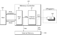
도 1은 본 발명의 실시예에 따른 메모리 컨트롤러를 개략적으로 도시한 블록도이다.
도 2는 본 발명의 실시예에 따른 메모리 컨트롤러의 제1 버퍼 관리 동작을 설명하기 위한 블록도이다.
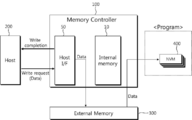
도 3은 본 발명의 실시예에 따른 메모리 컨트롤러의 제2 버퍼 관리 동작을 설명하기 위한 블록도이다.
도 4는 본 발명의 실시예에 따른 메모리 컨트롤러의 버퍼 관리 동작을 설명하기 위한 순서도이다.
도 5는 본 발명의 실시예에 따른 스토리지 디바이스를 개략적으로 도시한 블록도이다.
도 6은 본 발명의 실시예에 따른 스토리지 디바이스를 SSD(Solid State Drive)에 적용한 예를 도시한 블록도이다.1 is a block diagram schematically illustrating a memory controller according to an embodiment of the present invention.
2 is a block diagram illustrating a first buffer management operation of a memory controller according to an exemplary embodiment of the present invention.
3 is a block diagram illustrating a second buffer management operation of the memory controller according to an embodiment of the present invention.
4 is a flowchart illustrating a buffer management operation of a memory controller according to an embodiment of the present invention.
5 is a block diagram schematically illustrating a storage device according to an embodiment of the present invention.
6 is a block diagram illustrating an example in which a storage device according to an embodiment of the present invention is applied to a solid state drive (SSD).
본 발명의 목적, 특정한 장점들 및 신규한 특징들은 첨부된 도면들과 연관되어지는 이하의 상세한 설명과 바람직한 실시예들로부터 더욱 명백해질 것이다. 본 명세서에서 각 도면의 구성요소들에 참조번호를 부가함에 있어서, 동일한 구성 요소들에 한해서는 비록 다른 도면상에 표시되더라도 가능한 한 동일한 번호를 가지도록 하고 있음에 유의하여야 한다. 또한, "제1", "제2" 등의 용어는 하나의 구성요소를 다른 구성요소로부터 구별하기 위해 사용되는 것으로, 구성요소가 상기 용어들에 의해 제한되는 것은 아니다. 이하, 본 발명을 설명함에 있어서, 본 발명의 요지를 불필요하게 흐릴 수 있는 관련된 공지 기술에 대한 상세한 설명은 생략한다.The objects, specific advantages and novel features of the present invention will become more apparent from the following detailed description taken in conjunction with the accompanying drawings and preferred embodiments. In the present specification, in adding reference numbers to the components of each drawing, it should be noted that only the same components are given the same number as possible even though they are indicated on different drawings. Also, terms such as “first” and “second” are used to distinguish one component from another, and the component is not limited by the terms. Hereinafter, in describing the present invention, detailed descriptions of related known technologies that may unnecessarily obscure the gist of the present invention will be omitted.
이하, 첨부된 도면을 참조하여 본 발명의 바람직한 실시형태를 상세히 설명하기로 한다.Hereinafter, preferred embodiments of the present invention will be described in detail with reference to the accompanying drawings.
도 1은 본 발명의 실시예에 따른 메모리 컨트롤러를 개략적으로 도시한 블록도이고, 도 2는 본 발명의 실시예에 따른 메모리 컨트롤러의 제1 버퍼 관리 동작을 설명하기 위한 블록도이며, 도 3은 본 발명의 실시예에 따른 메모리 컨트롤러의 제2 버퍼 관리 동작을 설명하기 위한 블록도이다.1 is a block diagram schematically illustrating a memory controller according to an embodiment of the present invention, FIG. 2 is a block diagram illustrating a first buffer management operation of the memory controller according to an embodiment of the present invention, and FIG. 3 is It is a block diagram for explaining a second buffer management operation of the memory controller according to an embodiment of the present invention.
도 1 내지 도 3에 도시된 바와 같이, 본 발명의 실시예에 따른 메모리 컨트롤러(100)는 호스트(200)의 쓰기 요청(write request)에 대응하여, 외부 메모리(300)에 쓰기 데이터를 버퍼링(buffering)하고, 버퍼링된 쓰기 데이터를 비휘발성 메모리(400)에 프로그램(program)하는 메모리 컨트롤러에 있어서, 쓰기 데이터가 중복하여 버퍼링될 수 있는 내장 메모리(10), 및 내장 메모리(10)에 쓰기 데이터가 버퍼링될 수 있는 유휴 버퍼 공간의 존부를 확인하는 버퍼 공간 확인부(20), 및 버퍼 공간 확인부(20)에 의해 유휴 버퍼 공간의 존재가 확인된 때에, 외부 메모리(300)와 내장 메모리(10) 각각에 쓰기 데이터를 중복 버퍼링하는 제1 버퍼 관리 동작을 수행하는 버퍼 관리부(30)를 포함한다.1 to 3 , the
본 발명은 적어도 하나 이상의 비휘발성 메모리(400)를 제어하는 메모리 컨트롤러(100)에 관한 것이다. 비휘발성 메모리(400)는 본 발명에 따른 메모리 컨트롤러(100)에 의해 제어되고, 전원 공급이 차단되어도 데이터를 보존할 수 있는 스토리지 미디어(storage media)로서, 메모리 컨트롤러(100)의 명령에 대응하여 읽기(read), 프로그램(program) 등과 같은 동작들을 수행한다. 이러한 비휘발성 메모리(400)의 일례로는 EPROM, EEPROM, FRAM, PRAM, MRAM, 플래시 메모리(Flash Memory) 등을 들 수 있다. The present invention relates to a
비휘발성 메모리가 미디어로 채용된 종래 스토리지 디바이스의 경우에 호스트의 읽기/쓰기(read/write) 요청에 대한 처리 성능을 높이기 위하여 휘발성 외부 메모리를 버퍼(buffer)로 사용한다. 그러나 호스트의 쓰기 명령 처리 과정에서 외부 메모리에 대한 호스트 데이터 및 각종 메타 데이터 트래픽(data traffic)이 스토리지 미디어에 대한 호스트 데이터 트래픽 대비 매우 많기 때문에 외부 메모리에 성능 병목이 발생할 수 있다. 또한, 외부 메모리에 자주 읽기/쓰기(read/write)를 하는 경우, 입출력 전력으로 인한 전력 소모가 과도하게 발생하는 문제가 있는바, 이에 대한 해결방안으로서 본 발명이 안출되었다.In the case of a conventional storage device employing a non-volatile memory as a medium, a volatile external memory is used as a buffer in order to increase processing performance for a read/write request from a host. However, in the process of processing the host's write command, since host data and various types of metadata traffic to the external memory are much larger than the host data traffic to the storage medium, a performance bottleneck may occur in the external memory. In addition, there is a problem in that excessive power consumption due to input/output power occurs when frequently reading/writing an external memory is performed. As a solution to this problem, the present invention has been devised.
구체적으로, 본 발명의 실시예에 따른 메모리 컨트롤러(100)는, 내장 메모리(10), 버퍼 공간 확인부(20), 및 버퍼 관리부(30)를 포함한다. Specifically, the
또한, 호스트(200)와의 인터페이스를 제공하는 호스트 인터페이스(50)를 더 포함할 수 있다. 호스트 인터페이스(50)는 하나 또는 그보다 많은 채널들 또는 포트들(도시되지 않음)을 통해 호스트(200)와 연결될 수 있다. 예를 들면, 호스트 인터페이스(50)는 PATA 버스(parallel AT attachment bus), SATA 버스(serial AT attachment), PCIe 버스(peripheral component interconnect express) 중 어느 하나 또는 이들 모두를 통해 호스트(200)와 연결될 수 있다. 또는, SCSI, USB 등을 통해 외부와 연결될 수도 있다. 이러한 호스트 인터페이스(50)를 통해 호스트(200)로부터 쓰기 요청(write request) 및/또는 읽기 요청(read request)을 수신하고, 그 요청에 대응하는 처리가 완료된 경우에 처리 완료 응답(completion)을 호스트(200)로 전달할 수 있다.In addition, a
본 발명의 실시예에 따른 메모리 컨트롤러(100)는 호스트(200)의 쓰기 요청(write request)에 대응하여, 외부 메모리(300)에 대한 쓰기 버퍼링(write buffering) 및 버퍼 플러시(buffer flush)를 수행할 수 있다. 호스트(200)로부터 쓰기 요청을 수신하면, 외부 메모리(300)에 버퍼 공간을 할당하고, 할당된 버퍼 공간에 호스트(200)의 쓰기 데이터를 임시 저장한 후에, 호스트(200)에게 쓰기 컴플리션(write completion)을 전송하는데, 이러한 처리 동작을 쓰기 버퍼링 동작이라고 한다. 또한, 버퍼링된 데이터를 비휘발성 메모리(400)에 프로그램(program)하기 위해서, 프로그램 커맨드를 메모리 채널 컨트롤러(도시되지 않음)로 전송하고, 프로그램 컴플리션(program completion)을 수신하면, 데이터가 저장된 위치를 맵핑 테이블(mapping table)에 기록하고, 할당된 버퍼 공간을 해제한다. 이상의 처리 동작을 버퍼 플러시 동작이라고 한다. 상기 쓰기 버퍼링을 통해 호스트(200)로 빠르게 컴플리션이 가능하므로 쓰기 레이턴시(write latency)가 향상된다. 버퍼 플러시는 백그라운드(background)로 수행되기 때문에 통상의 경우에 호스트(200)가 체감하는 성능에 영향을 미치지는 않지만, 버퍼 플러시가 너무 늦게 되면 외부 메모리(300)에 할당 가능한 공간이 고갈되므로 이후의 호스트(200) 쓰기 커맨드에 대한 레이턴시가 길어질 수 있다.The
한편, 호스트(200)의 읽기 요청에 대응해서는, 먼저 읽기 요청된 데이터가 버퍼 공간에 존재하는지 검색한다. 버퍼 내에 데이터가 존재하면, 버퍼에서 호스트(200)로 데이터를 전송하고 컴플리션을 전송한다. 반면, 버퍼 데이터가 존재하지 않으면, 맵핑 테이블을 참조하여 데이터가 위치한 비휘발성 메모리(400) 상의 물리적 주소(physical address)를 얻어 메모리 채널 컨트롤러에 읽기 커맨드를 전송하고, 이에 따라 호스트(200)로 비휘발성 메모리(400)의 데이터 및 컴플리션을 전달한다.Meanwhile, in response to the read request of the
다만, 전술한 바와 같이 외부 메모리(300)를 버퍼로 사용하는 경우에 외부 메모리(300)의 성능 병목 및 전력 소모가 문제되는바, 본 발명에 따른 메모리 컨트롤러(100)는 외부 메모리(300) 이외에 내장 메모리(10)를 구비하고, 외부 메모리(300)에 대한 접근 빈도를 최소화할 수 있도록 외부 메모리 및 내장 메모리의 버퍼(buffer)를 관리한다.However, as described above, when the
내장 메모리(10)는 본 발명에 따른 메모리 컨트롤러(100)의 내부에 장착되는 메모리이다. 내장 메모리(10)는 휘발성 램(RAM), 일례로 SRAM 등으로 구현될 수 있다. 또한, 내장 메모리(10)는 하나의 메모리 블록이나, 또는 비휘발성 메모리(400)의 각 영역에 대응하는 복수의 메모리 블록들로 구성되어 내장될 수 있다. 일반적으로 내장 메모리(10)는 외부 메모리(300)에 비해 저장 용량은 작지만 접근 속도가 빠르고 전력 소모가 작다. 이러한 내장 메모리(10)는 쓰기 버퍼로 사용된다. 따라서, 호스트 인터페이스(60)를 통해 쓰기 요청이 수신된 경우에, 기 설정된 조건 하에서, 그 쓰기 요청에 대응하여 비휘발성 메모리(400)에 프로그램될 쓰기 데이터가 내장 메모리(10)에 일시 저장, 즉 버퍼링될 수 있다. 다만, 내장 메모리(10)가 반드시 쓰기 버퍼로만 사용되어야 하는 것은 아니고, 후술하는 프로세서(50)에 의해서 실행되는 소프트웨어 코드나 각종 변수(variable)와 같이 소프트웨어가 처리하는 데이터를 저장할 수 있다. 또한, 저속의 비휘발성 메모리(400)에서 유지되는 자료 구조에 대한 고속 접근을 가능하게 한다. 예를 들어, 맵핑 테이블(mapping table)을 내장 메모리(10) 상에서 관리하며 주기적으로 비휘발성 메모리(400)로 맵핑 테이블을 덤프(dump)할 수 있다. 또한, 비휘발성 메모리(400)가 플래시 메모리인 경우에 소위 플래시 변환 계층(FTL)으로 불리는 소프트웨어를 구동하기 위한 구동 메모리로 사용될 수 있다. The built-in
버퍼 공간 확인부(20)는 내장 메모리(10)를 대상으로 쓰기 버퍼링이 가능한지를 확인한다. 내장 메모리(10)는 버퍼 공간을 구비하는데, 수신된 호스트(200)의 쓰기 요청에 대응되는 쓰기 데이터가 버퍼링될 수 있는 유휴 버퍼 공간의 존부를 확인한다. 내장 메모리(10)에 소프트웨어 처리를 위한 데이터 및 기 버퍼링된 쓰기 데이터가 저장되기 때문에, 버퍼 공간 확인부(20)는 쓰기 버퍼링 동작을 수행하기 위해 먼저 내장 메모리(10)에 유휴 버퍼 공간이 존재하는지를 검색한다. The buffer
버퍼 관리부(30)는 수신된 호스트(200)의 쓰기 요청에 대응하여 해당 쓰기 데이터를 버퍼링하는 버퍼 관리 동작을 수행한다. 버퍼 관리 동작은 제1 버퍼 관리 동작과 제2 버퍼 관리 동작으로 구분되고, 내장 메모리(10)에 유휴 버퍼 공간이 존재하는 경우에 제1 버퍼 관리 동작이 수행되고, 내장 메모리(10)에 유휴 버퍼 공간이 부존재하는 경우에 제2 버퍼 관리 동작이 수행된다.The
버퍼 공간 확인부(20)에 의해 버퍼링 가능한 유휴 버퍼 공간이 존재하는 것으로 확인되면, 제1 버퍼 관리 동작에 따라, 해당 쓰기 데이터는 내장 메모리(10)와 외부 메모리(300)에 중복되어 버퍼링된다(도 2 참조). 즉, 쓰기 데이터가 내장 메모리(10) 및 외부 메모리(300) 각각에 임시로 저장된다. 한편, 중복 버퍼링되는 쓰기 데이터가 비휘발성 메모리(400)에 프로그램되도록 플러시 동작이 수행될 때, 내장 메모리(10)에 버퍼링된 쓰기 데이터가 비휘발성 메모리(400)로 전송되고, 전송된 쓰기 데이터가 점유했던 내장 메모리(10)의 버퍼 공간은 점유 해제될 수 있다. 즉, 내장 메모리(10)에서 전송된 쓰기 데이터의 프로그램 성공 여부와 무관하게, 쓰기 데이터를 위해 내장 메모리(10)에 할당되었던 버퍼 공간은 점유 해제된다. 여기서, 내장 메모리(10)에서 전송된 쓰기 데이터의 프로그램이 성공되면, 외부 메모리(300)에 중복 버퍼링된 쓰기 데이터가 삭제되고 그 버퍼 공간도 점유 해제될 수 있다. 반면, 내장 메모리(10)에서 전송된 쓰기 데이터의 프로그램이 실패되는 경우에는, 외부 메모리(300)에 중복 버퍼링된 쓰기 데이터를 전송하여 프로그램 동작을 재수행하고, 프로그램이 성공되면 외부 메모리(300)에 할당되었던 버퍼 공간이 점유 해제될 수 있다. 통상 프로그램이 실패하는 경우는 매우 드물기 때문에 플러시 동작은 대부분 내장 메모리(10)에서 수행된다. 따라서, 외부 메모리(300)만을 버퍼로 사용하는 경우에 비해, 외부 메모리(300)에 대한 접근 횟수를 대략 절반으로 줄일 수 있다.If it is confirmed by the buffer
버퍼 공간 확인부(20)에 의해 버퍼링 가능한 유휴 버퍼 공간이 부존재하는 것으로 확인되면, 제2 버퍼 관리 동작에 따라, 내장 메모리(10)로의 버퍼링을 생략하고 외부 메모리(300)에만 해당 쓰기 데이터가 버퍼링될 수 있다(도 3 참조). 여기서, 본 발명에 따른 메모리 컨트롤러(100)는 외부 메모리(300)에 버퍼 공간을 할당하고, 할당된 버퍼 공간에 해당 쓰기 데이터를 임시 저장한 후, 호스트(200)에게 쓰기 컴플리션(write completion)을 전송할 수 있다. 또한, 버퍼링된 데이터를 비휘발성 메모리(400)에 프로그램(program)하기 위해서, 메모리 채널 컨트롤러(도시되지 않음)를 통해 버퍼링된 데이터를 전송하고, 프로그램이 완료되면, 할당되었던 버퍼 공간을 해제할 수 있다.When it is confirmed by the buffer
내장 메모리(10) 및 외부 메모리(300)에 버퍼링된 쓰기 데이터가 비휘발성 메모리(400)에 프로그램되도록 수행되는 플러시 동작은 플러시 동작부(40)에 의해 처리될 수 있다. 따라서, 제1 버퍼 관리 동작에 따라, 내장 메모리(10) 및 외부 메모리(300)에 버퍼링된 쓰기 데이터는, 플러시 동작부(40)에 의해 비휘발성 메모리(400)로 전송되고 프로그램된다. 이때, 내장 메모리(10)에 버퍼링된 쓰기 데이터에 대해 우선적으로 플러시 동작이 수행되고, 이에 의한 프로그램이 실패된 경우에 외부 메모리(300)에 버퍼링된 쓰기 데이터가 프로그램된다. 또한, 제2 버퍼 관리 동작에 따라, 외부 메모리(300)에 버퍼링된 쓰기 데이터도, 플러시 동작부(40)에 의해 비휘발성 메모리(400)로 전송되고 프로그램된다. A flush operation performed so that write data buffered in the
한편, 본 발명에 따른 메모리 컨트롤러는 호스트(200)로부터 수신된 호스트(200) 요청을 처리하는 프로세서(도시되지 않음)를 더 포함할 수 있다. 프로세서는 마이크로 컨트롤 유닛(MCU), 중앙처리장치(CPU) 등으로 구현될 수 있다. 프로세서는 소프트웨어를 구동하여, 내부의 기능 블록들 및 비휘발성 메모리(400)를 제어할 수 있다. 여기서, 구동되는 소프트웨어는 내장 메모리(10)에 저장될 수 있고, 소프트웨어의 구동에 필요한 데이터도 여기에 저장될 수 있다. 다만, 상기 소프트웨어 및 구동에 필요한 데이터가 반드시 내장 메모리(10)에 저장되어야 하는 것은 아니다.Meanwhile, the memory controller according to the present invention may further include a processor (not shown) for processing the
여기서, 버퍼 공간 확인부(20), 및 버퍼 관리부(30)는 하드웨어 또는 소프트웨어로 구현될 수 있다. 즉, 메모리 컨트롤러(100)의 내부에 위치한 디지털 또는 아날로그 회로 형태로 구현되거나, 별도의 칩 또는 모듈로 구현되어 메모리 컨트롤러(100)에 연결될 수 있으며, SRAM과 같은 내장 메모리(10)나 플로피 디스크, 컴팩트 디스크, USB 등과 같은 외부 메모리(300)에 소프트웨어를 저장하고 실행하는 방식으로 구현될 수 있다. 또한, 사용자에 의해 프로그램될 수 있는 형태로 구현될 수도 있다. 나아가, 프로세서에 통합될 수도 있다. Here, the buffer
종합적으로, 본 발명에 따른 메모리 컨트롤러(100)에 따르면, 쓰기 버퍼링을 수행하는 외부 메모리(300) 이외에 버퍼 공간을 가지는 내장 메모리(10)를 구비하고, 외부 메모리(300)에 대한 접근 빈도를 최소화할 수 있도록 외부 메모리(300) 및 내장 메모리(10)의 버퍼(buffer)를 관리함으로써, 외부 메모리(300)의 성능 병목 및 과도한 전력 소모를 방지할 수 있다.Overall, according to the
한편, 호스트 인터페이스(50)가 호스트(200)로부터 읽기 요청(read request)을 수신한 경우에, 본 발명에 따른 메모리 컨트롤러(100)는 1차적으로 내장 메모리(10)에 그 읽기 요청에 대응되는 읽기 데이터가 존재하는지 검색하고, 읽기 데이터가 존재하면 호스트(200)로 그 읽기 데이터를 전송할 수 있다. 만약, 내장 메모리(10)에 읽기 데이터가 존재하지 않으면, 2차적으로 외부 메모리(300)를 검색하여, 외부 메모리(300)에 존재하는 읽기 데이터를 호스트(200)로 전달하고, 외부 메모리(300)에도 읽기 데이터가 존재하지 않으면 비휘발성 메모리(400)로부터 읽기 데이터를 호스트(200)로 전달할 수 있다. 다만, 내장 메모리(10)와 외부 메모리(300)에 대한 버퍼 검사 순서가 반드시 이에 한정되어야 하는 것은 아니고, 외부 메모리(300)를 먼저 검사하고 다음에 내장 메모리(10)를 검사해도 무방하다. 단, 내장 메모리(10)와 외부 메모리(300) 모두에 데이터가 존재하는 경우에는, 내장 메모리(10)에서 데이터를 전송하는 것이 이득이므로, 내장 메모리(10)부터 검사하는 것이 바람직하다.On the other hand, when the
이하에서는 도 4를 들어 본 발명에 따른 메모리 컨트롤러의 버퍼 관리 동작을 보다 자세하게 설명한다. 도 4는 본 발명의 실시예에 따른 메모리 컨트롤러의 버퍼 관리 동작을 설명하기 위한 순서도이다.Hereinafter, a buffer management operation of the memory controller according to the present invention will be described in detail with reference to FIG. 4 . 4 is a flowchart illustrating a buffer management operation of a memory controller according to an embodiment of the present invention.
도 4를 참고로, 메모리 컨트롤러가 쓰기 요청을 수신한 경우, 내장 메모리(IntM)의 쓰기 버퍼가 풀(full) 상태인지 검사한다. 내장 메모리(IntM)가 풀 상태가 아니면, 내장 메모리(IntM) 및 외부 메모리(ExtM) 각각에 버퍼 영역을 할당하고, 쓰기 요청에 대응되는 해당 쓰기 데이터를 내장 메모리(IntM) 및 외부 메모리(ExtM)에 전달한다. 다음에, 해당 쓰기 데이터의 논리 블록 주소(LBA, Logical Block Address)를 내장 메모리(IntM) 및 외부 메모리(ExtM) 쓰기 버퍼 LBA 리스트에 삽입하고, 처리 완료 응답(completion)을 호스트에 전달한다. 그리고 나서, 내장 메모리(IntM)의 쓰기 버퍼에서 쓰기 데이터를 스토리지 미디어(NVM)로 전송하여, 스토리지 미디어에 기입(프로그램)한다. 이때, 기입이 완료될 때까지 기다리지 않고, 내장 메모리(IntM) 쓰기 버퍼 LBA 리스트에서 해당 LBA를 삭제한다. 내장 메모리(IntM)에서 전달된 쓰기 데이터가 스토리지 미디어에 기입(프로그램)되는 경우, LBA를 물리 주소로 변환하는 맵핑(LBA-to-physical address) 정보 업데이트를 수행하고, 외부 메모리(ExtM) 쓰기 버퍼 LBA 리스트에서 해당 LBA를 삭제한다. 한편, 내장 메모리(IntM)에서 전달된 쓰기 데이터가 프로그램되지 못하는 경우에는, 외부 메모리(ExtM)의 쓰기 버퍼에서 쓰기 데이터를 스토리지 미디어(NVM)로 전송하여, 프로그램 동작을 재실행하고, 프로그램이 성공적으로 완료되면, LBA를 물리 주소로 변환하는 맵핑(LBA-to-physical address) 정보 업데이트를 수행한 후, 외부 메모리(ExtM) 쓰기 버퍼 LBA 리스트에서 해당 LBA를 삭제한다.Referring to FIG. 4 , when the memory controller receives a write request, it is checked whether the write buffer of the internal memory IntM is in a full state. If the internal memory (IntM) is not in the full state, a buffer area is allocated to each of the internal memory (IntM) and the external memory (ExtM), and the corresponding write data corresponding to the write request is transferred to the internal memory (IntM) and external memory (ExtM) forward to Next, a logical block address (LBA) of the corresponding write data is inserted into the internal memory (IntM) and external memory (ExtM) write buffer LBA lists, and a completion response is transmitted to the host. Then, write data is transferred from the write buffer of the internal memory IntM to the storage medium NVM, and written (programmed) to the storage medium. At this time, the LBA is deleted from the internal memory (IntM) write buffer LBA list without waiting until the writing is completed. When write data transferred from the internal memory (IntM) is written (programmed) to the storage medium, LBA-to-physical address information is updated, which converts the LBA to a physical address, and the external memory (ExtM) write buffer Delete the LBA from the LBA list. On the other hand, if the write data transferred from the internal memory (IntM) cannot be programmed, the write data is transferred from the write buffer of the external memory (ExtM) to the storage media (NVM) to re-execute the program operation, and the program is successfully executed. Upon completion, the LBA-to-physical address information is updated, and the LBA is deleted from the external memory (ExtM) write buffer LBA list.
반면, 내장 메모리(IntM)의 쓰기 버퍼가 풀(full) 상태인 경우에는, 외부 메모리(ExtM)에 해당 쓰기 데이터를 전달하고, 해당 쓰기 데이터의 논리 블록 주소(LBA, Logical Block Address)를 외부 메모리(ExtM) 쓰기 버퍼 LBA 리스트에 삽입한 후, 처리 완료 응답(completion)을 호스트에 전달한다. 다음, 쓰기 데이터를 외부 메모리(ExtM)의 쓰기 버퍼에서 스토리지 미디어(NVM)로 전달하여, 스토리지 미디어에 기입(프로그램)한다. 외부 메모리(ExtM)에서 전달된 쓰기 데이터가 스토리지 미디어에 기입(프로그램)되는 경우, LBA를 물리 주소로 변환하는 맵핑(LBA-to-physical address) 정보 업데이트를 수행하고, 외부 메모리(ExtM) 쓰기 버퍼 LBA 리스트에서 해당 LBA를 삭제한다. 한편, 외부 메모리(ExtM)에서 전달된 쓰기 데이터가 프로그램되지 못하는 경우에는, 프로그램 동작을 재실행한다.On the other hand, when the write buffer of the internal memory (IntM) is in the full state, the write data is transferred to the external memory (ExtM), and the logical block address (LBA, Logical Block Address) of the write data is set to the external memory. (ExtM) After inserting into the write buffer LBA list, a processing completion response (completion) is transmitted to the host. Next, write data is transferred from the write buffer of the external memory (ExtM) to the storage medium (NVM) and written (programmed) to the storage medium. When write data transferred from the external memory (ExtM) is written (programmed) to the storage medium, LBA-to-physical address information update that converts the LBA into a physical address is updated, and the external memory (ExtM) write buffer Delete the LBA from the LBA list. Meanwhile, when the write data transferred from the external memory ExtM is not programmed, the program operation is re-executed.
본 발명에 따른 메모리 컨트롤러는 스토리지 디바이스에 적용될 수 있는데, 이하에서 이에 대해 설명한다.The memory controller according to the present invention can be applied to a storage device, which will be described below.
도 5는 본 발명의 실시예에 따른 스토리지 디바이스를 개략적으로 도시한 블록도이고, 도 6은 본 발명의 실시예에 따른 스토리지 디바이스를 SSD(Solid State Drive)에 적용한 예를 도시한 블록도이다.5 is a block diagram schematically illustrating a storage device according to an embodiment of the present invention, and FIG. 6 is a block diagram illustrating an example in which the storage device according to an embodiment of the present invention is applied to a solid state drive (SSD).
도 7에 도시된 바와 같이, 본 발명의 실시예에 따른 스토리지 디바이스(1000)는 메모리 컨트롤러(100), 호스트(200)의 쓰기 요청(write request)에 대응하여, 쓰기 데이터가 버퍼링(buffering)될 수 있는 외부 메모리(300), 및 버퍼링된 쓰기 데이터가 프로그램되는 비휘발성 메모리(400)를 포함한다.7 , in response to a write request from the
여기서, 메모리 컨트롤러(100), 외부 메모리(300), 및 비휘발성 메모리(400)에 관한 사항은 전술한 바와 동일하므로, 이에 대한 구체적인 설명은 생략한다.Here, since the
스토리지 디바이스(1000)는 메모리 카드나 착탈 가능한 이동식 저장 장치를 포함할 수 있다. 스토리지 디바이스(1000)는 호스트(200)와 연결되어 사용되고, 호스트 인터페이스를 통해 호스트(200)와 데이터를 주고받는다. 이때, 스토리지 디바이스(1000)는 호스트(200)로부터 전원을 공급받아 내부 동작을 수행할 수 있다.The
또한, 도 8을 참고로, 본 발명에 따른 스토리지 디바이스(1000)는 솔리드 스테이트 드라이브(Solid State Drive, SSD)일 수 있다. Also, referring to FIG. 8 , the
SSD는 호스트(200)와 연결되기 때문에, 호스트(200)는 SSD에 데이터를 쓰거나 SSD에 저장된 데이터를 읽을 수 있다. SSD는 호스트 인터페이스를 통해 호스트(200)와 신호를 교환하고 전원 커넥터를 통해 전원을 공급받을 수 있다. SSD는 다수의 비휘발성 메모리(400), 및 SSD 컨트롤러를 포함할 수 있는데, 여기서 비휘발성 메모리(400)는 플래시 메모리 이외에도 PRAM, MRAM, ReRAM, FRAM 등으로 구현될 수 있고, 복수의 비휘발성 메모리(400)가 복수의 채널을 통해 SSD 컨트롤러와 연결될 수 있다. 이때, 하나의 채널에는 하나 또는 그 이상의 비휘발성 메모리(400)가 연결될 수 있고, 하나의 채널에 연결되는 비휘발성 메모리(400)는 동일한 데이터 버스에 연결될 수 있다.Since the SSD is connected to the
한편, 본 발명에 따른 메모리 컨트롤러(100)는 SSD 컨트롤러로서 제공되어, 호스트 인터페이스를 통해 호스트(200)와 신호를 주고받는다. 여기서, 신호를 통해 커맨드, 어드레스, 데이터 등이 전달될 수 있고, 호스트(200)의 커맨드에 따라 해당 비휘발성 메모리(400)에 데이터를 기입하거나 해당 비휘발성 메모리(400)로부터 데이터를 독출해낸다. Meanwhile, the
이상 본 발명을 구체적인 실시예를 통하여 상세히 설명하였으나, 이는 본 발명을 구체적으로 설명하기 위한 것으로, 본 발명은 이에 한정되지 않으며, 본 발명의 기술적 사상 내에서 당 분야의 통상의 지식을 가진 자에 의해 그 변형이나 개량이 가능함이 명백하다.Although the present invention has been described in detail through specific examples, this is for the purpose of describing the present invention in detail, and the present invention is not limited thereto. It is clear that the modification or improvement is possible.
본 발명의 단순한 변형 내지 변경은 모두 본 발명의 영역에 속한 것으로 본 발명의 구체적인 보호 범위는 첨부된 특허청구범위에 의하여 명확해질 것이다.All simple modifications or changes of the present invention are within the scope of the present invention, and the specific scope of protection of the present invention will be made clear by the appended claims.
10: 내장 메모리 20: 버퍼 공간 확인부
30: 버퍼 관리부 40: 플러시 동작부
50: 호스트 인터페이스 100: 메모리 컨트롤러
200: 호스트 300: 외부 메모리
400: 비휘발성 메모리 1000: 스토리지 디바이스10: Built-in memory 20: Buffer space confirmation unit
30: buffer management unit 40: flush operation unit
50: host interface 100: memory controller
200: host 300: external memory
400: non-volatile memory 1000: storage device
Claims (7)
상기 쓰기 데이터가 중복하여 버퍼링될 수 있는 내장 메모리;
상기 내장 메모리에 상기 쓰기 데이터가 버퍼링될 수 있는 유휴 버퍼 공간의 존부를 확인하는 버퍼 공간 확인부; 및
상기 버퍼 공간 확인부에 의해 상기 유휴 버퍼 공간의 존재가 확인된 때에, 상기 외부 메모리와 상기 내장 메모리 각각에 상기 쓰기 데이터를 중복 버퍼링하는 제1 버퍼 관리 동작을 수행하는 버퍼 관리부;를 포함하고,
상기 버퍼 관리부는,
상기 버퍼 공간 확인부에 의해 상기 유휴 버퍼 공간의 부존재가 확인된 때에, 상기 내장 메모리로의 버퍼링을 생략하고 상기 외부 메모리에만 상기 쓰기 데이터를 버퍼링하는 제2 버퍼 관리 동작을 수행하는 메모리 컨트롤러.
A memory controller for buffering write data in an external memory in response to a write request from a host, and programming the buffered write data in a non-volatile memory, the memory controller comprising:
an internal memory in which the write data can be overlapped and buffered;
a buffer space check unit for checking whether there is an idle buffer space in which the write data can be buffered in the built-in memory; and
a buffer management unit that performs a first buffer management operation of redundantly buffering the write data in each of the external memory and the internal memory when the existence of the idle buffer space is confirmed by the buffer space checking unit;
The buffer management unit,
The memory controller performs a second buffer management operation of omitting buffering to the internal memory and buffering the write data only in the external memory when the absence of the idle buffer space is confirmed by the buffer space check unit.
상기 제1 버퍼 관리 동작에 의해 상기 내장 메모리 및 상기 외부 메모리에 버퍼링된 상기 쓰기 데이터가 상기 비휘발성 메모리에 프로그램되도록 플러시(flush) 동작을 수행하는 플러시 동작부;를 더 포함하는 메모리 컨트롤러.
The method according to claim 1,
and a flush operation unit configured to perform a flush operation so that the write data buffered in the internal memory and the external memory are programmed into the nonvolatile memory by the first buffer management operation.
상기 플러시 동작부는,
상기 내장 메모리에 중복 버퍼링된 상기 쓰기 데이터를, 상기 비휘발성 메모리에 전송하고, 전송된 상기 쓰기 데이터가 점유했던 상기 내장 메모리의 버퍼 공간을 점유 해제하며,
전송된 상기 쓰기 데이터의 프로그램이 실패된 경우에, 상기 외부 메모리에 중복 버퍼링된 상기 쓰기 데이터를, 상기 비휘발성 메모리에 전송하는 메모리 컨트롤러.
4. The method according to claim 3,
The flush operation unit,
transferring the write data duplicately buffered in the built-in memory to the non-volatile memory, and releasing a buffer space of the built-in memory occupied by the transmitted write data;
The memory controller transmits the write data duplicately buffered in the external memory to the non-volatile memory when the program of the transmitted write data fails.
상기 내장 메모리는, 휘발성 램(RAM)인 메모리 컨트롤러.
The method according to claim 1,
The internal memory is a volatile RAM (RAM) memory controller.
호스트의 쓰기 요청(write request)에 대응하여, 쓰기 데이터가 버퍼링(buffering)될 수 있는 외부 메모리; 및
버퍼링된 상기 쓰기 데이터가 프로그램되는 비휘발성 메모리;를 포함하는 스토리지 디바이스.
The memory controller according to any one of claims 1 and 3 to 5;
an external memory in which write data can be buffered in response to a write request of the host; and
and a non-volatile memory into which the buffered write data is programmed.
상기 비휘발성 메모리는 플래시 메모리인 스토리지 디바이스.
7. The method of claim 6,
wherein the non-volatile memory is a flash memory.
Priority Applications (2)
| Application Number | Priority Date | Filing Date | Title |
|---|---|---|---|
| KR1020200181896A KR102343600B1 (en) | 2020-12-23 | 2020-12-23 | Memory controller and storage device including the same |
| US17/557,479 US20220197548A1 (en) | 2020-12-23 | 2021-12-21 | Memory controller and storage device including the same |
Applications Claiming Priority (1)
| Application Number | Priority Date | Filing Date | Title |
|---|---|---|---|
| KR1020200181896A KR102343600B1 (en) | 2020-12-23 | 2020-12-23 | Memory controller and storage device including the same |
Publications (1)
| Publication Number | Publication Date |
|---|---|
| KR102343600B1 true KR102343600B1 (en) | 2021-12-27 |
Family
ID=79177021
Family Applications (1)
| Application Number | Title | Priority Date | Filing Date |
|---|---|---|---|
| KR1020200181896A Active KR102343600B1 (en) | 2020-12-23 | 2020-12-23 | Memory controller and storage device including the same |
Country Status (2)
| Country | Link |
|---|---|
| US (1) | US20220197548A1 (en) |
| KR (1) | KR102343600B1 (en) |
Citations (4)
| Publication number | Priority date | Publication date | Assignee | Title |
|---|---|---|---|---|
| KR940022295A (en) | 1993-03-20 | 1994-10-20 | 가나이 쯔또무 | Microcomputer with flash memory |
| KR101574207B1 (en) * | 2009-10-16 | 2015-12-14 | 삼성전자주식회사 | Data storage device and its data storage method |
| KR20200008476A (en) * | 2018-07-16 | 2020-01-28 | 에스케이하이닉스 주식회사 | Memory system and operating method thereof |
| KR20200055310A (en) * | 2018-11-13 | 2020-05-21 | 에스케이하이닉스 주식회사 | Data Storage Device and Operation Method Thereof, Storage System Having the Same |
Family Cites Families (5)
| Publication number | Priority date | Publication date | Assignee | Title |
|---|---|---|---|---|
| US6720893B2 (en) * | 2002-02-22 | 2004-04-13 | International Business Machines Corporation | Programmable output control of compressed data from encoder |
| JP4412981B2 (en) * | 2003-11-26 | 2010-02-10 | 株式会社日立製作所 | Storage system and data caching method in the same system |
| US7441081B2 (en) * | 2004-12-29 | 2008-10-21 | Lsi Corporation | Write-back caching for disk drives |
| CN106681692A (en) * | 2015-11-09 | 2017-05-17 | 联发科技(新加坡)私人有限公司 | Control device, integrated circuit and management method of task stack |
| US11726704B2 (en) * | 2020-03-31 | 2023-08-15 | Kioxia Corporation | Buffer optimization for solid-state drives |
-
2020
- 2020-12-23 KR KR1020200181896A patent/KR102343600B1/en active Active
-
2021
- 2021-12-21 US US17/557,479 patent/US20220197548A1/en not_active Abandoned
Patent Citations (4)
| Publication number | Priority date | Publication date | Assignee | Title |
|---|---|---|---|---|
| KR940022295A (en) | 1993-03-20 | 1994-10-20 | 가나이 쯔또무 | Microcomputer with flash memory |
| KR101574207B1 (en) * | 2009-10-16 | 2015-12-14 | 삼성전자주식회사 | Data storage device and its data storage method |
| KR20200008476A (en) * | 2018-07-16 | 2020-01-28 | 에스케이하이닉스 주식회사 | Memory system and operating method thereof |
| KR20200055310A (en) * | 2018-11-13 | 2020-05-21 | 에스케이하이닉스 주식회사 | Data Storage Device and Operation Method Thereof, Storage System Having the Same |
Also Published As
| Publication number | Publication date |
|---|---|
| US20220197548A1 (en) | 2022-06-23 |
Similar Documents
| Publication | Publication Date | Title |
|---|---|---|
| CN113377283B (en) | Memory system with partitioned namespaces and method of operation thereof | |
| US9304691B2 (en) | Memory system and bank interleaving method | |
| US8775739B2 (en) | Memory system including first and second caches and controlling readout of data therefrom | |
| US9128618B2 (en) | Non-volatile memory controller processing new request before completing current operation, system including same, and method | |
| US9229655B2 (en) | Controller and method for performing background operations | |
| US9122611B2 (en) | Method for giving read commands and reading data, and controller and storage system using the same | |
| US9396141B2 (en) | Memory system and information processing device by which data is written and read in response to commands from a host | |
| KR20090019593A (en) | IC control circuit and multichannel memory system including the same | |
| US8914587B2 (en) | Multi-threaded memory operation using block write interruption after a number or threshold of pages have been written in order to service another request | |
| KR20200114212A (en) | Data storage device and operating method thereof | |
| US9990280B2 (en) | Methods for reading data from a storage unit of a flash memory and apparatuses using the same | |
| KR20190091035A (en) | Memory system and operating method thereof | |
| US11029854B2 (en) | Memory controller for concurrently writing host data and garbage collected data and operating method thereof | |
| US11556276B2 (en) | Memory system and operating method thereof | |
| KR100794312B1 (en) | A memory controller including an instruction automatic processing unit and a memory system including the same | |
| US11307786B2 (en) | Data storage devices and data processing methods | |
| KR102343600B1 (en) | Memory controller and storage device including the same | |
| US20150254011A1 (en) | Memory system, memory controller and control method of non-volatile memory | |
| KR102343599B1 (en) | Memory controller and storage device including the same | |
| US20220405215A1 (en) | Method for accessing flash memory and flash memory controller and electronic device thereof | |
| CN118369721A (en) | Storage system operation method, storage controller, storage system and electronic device | |
| US20140281160A1 (en) | Non-volatile semiconductor storage apparatus | |
| US12105990B2 (en) | Parallel fragmented SGL fetching for hiding host turnaround time | |
| JP7796255B2 (en) | HMB-based write coalescence for optimized write performance | |
| US20250044986A1 (en) | Skipping completion for repeat lbas based upon lba tracking |
Legal Events
| Date | Code | Title | Description |
|---|---|---|---|
| PA0109 | Patent application |
Patent event code: PA01091R01D Comment text: Patent Application Patent event date: 20201223 |
|
| PA0201 | Request for examination | ||
| PA0302 | Request for accelerated examination |
Patent event date: 20201223 Patent event code: PA03022R01D Comment text: Request for Accelerated Examination |
|
| PE0902 | Notice of grounds for rejection |
Comment text: Notification of reason for refusal Patent event date: 20210223 Patent event code: PE09021S01D |
|
| PE0701 | Decision of registration |
Patent event code: PE07011S01D Comment text: Decision to Grant Registration Patent event date: 20211025 |
|
| GRNT | Written decision to grant | ||
| PR0701 | Registration of establishment |
Comment text: Registration of Establishment Patent event date: 20211222 Patent event code: PR07011E01D |
|
| PR1002 | Payment of registration fee |
Payment date: 20211222 End annual number: 3 Start annual number: 1 |
|
| PG1601 | Publication of registration |