KR102343390B1 - Display device and manufacturing method of the same - Google Patents
Display device and manufacturing method of the same Download PDFInfo
- Publication number
- KR102343390B1 KR102343390B1 KR1020170043117A KR20170043117A KR102343390B1 KR 102343390 B1 KR102343390 B1 KR 102343390B1 KR 1020170043117 A KR1020170043117 A KR 1020170043117A KR 20170043117 A KR20170043117 A KR 20170043117A KR 102343390 B1 KR102343390 B1 KR 102343390B1
- Authority
- KR
- South Korea
- Prior art keywords
- organic layer
- layer
- organic
- silicon
- atomic ratio
- Prior art date
- Legal status (The legal status is an assumption and is not a legal conclusion. Google has not performed a legal analysis and makes no representation as to the accuracy of the status listed.)
- Active
Links
Images


Classifications
-
- C—CHEMISTRY; METALLURGY
- C23—COATING METALLIC MATERIAL; COATING MATERIAL WITH METALLIC MATERIAL; CHEMICAL SURFACE TREATMENT; DIFFUSION TREATMENT OF METALLIC MATERIAL; COATING BY VACUUM EVAPORATION, BY SPUTTERING, BY ION IMPLANTATION OR BY CHEMICAL VAPOUR DEPOSITION, IN GENERAL; INHIBITING CORROSION OF METALLIC MATERIAL OR INCRUSTATION IN GENERAL
- C23C—COATING METALLIC MATERIAL; COATING MATERIAL WITH METALLIC MATERIAL; SURFACE TREATMENT OF METALLIC MATERIAL BY DIFFUSION INTO THE SURFACE, BY CHEMICAL CONVERSION OR SUBSTITUTION; COATING BY VACUUM EVAPORATION, BY SPUTTERING, BY ION IMPLANTATION OR BY CHEMICAL VAPOUR DEPOSITION, IN GENERAL
- C23C16/00—Chemical coating by decomposition of gaseous compounds, without leaving reaction products of surface material in the coating, i.e. chemical vapour deposition [CVD] processes
- C23C16/22—Chemical coating by decomposition of gaseous compounds, without leaving reaction products of surface material in the coating, i.e. chemical vapour deposition [CVD] processes characterised by the deposition of inorganic material, other than metallic material
- C23C16/30—Deposition of compounds, mixtures or solid solutions, e.g. borides, carbides, nitrides
- C23C16/32—Carbides
- C23C16/325—Silicon carbide
-
- H01L51/5253—
-
- H—ELECTRICITY
- H10—SEMICONDUCTOR DEVICES; ELECTRIC SOLID-STATE DEVICES NOT OTHERWISE PROVIDED FOR
- H10K—ORGANIC ELECTRIC SOLID-STATE DEVICES
- H10K50/00—Organic light-emitting devices
- H10K50/80—Constructional details
- H10K50/84—Passivation; Containers; Encapsulations
- H10K50/844—Encapsulations
- H10K50/8445—Encapsulations multilayered coatings having a repetitive structure, e.g. having multiple organic-inorganic bilayers
-
- B—PERFORMING OPERATIONS; TRANSPORTING
- B32—LAYERED PRODUCTS
- B32B—LAYERED PRODUCTS, i.e. PRODUCTS BUILT-UP OF STRATA OF FLAT OR NON-FLAT, e.g. CELLULAR OR HONEYCOMB, FORM
- B32B27/00—Layered products comprising a layer of synthetic resin
- B32B27/06—Layered products comprising a layer of synthetic resin as the main or only constituent of a layer, which is next to another layer of the same or of a different material
-
- C—CHEMISTRY; METALLURGY
- C23—COATING METALLIC MATERIAL; COATING MATERIAL WITH METALLIC MATERIAL; CHEMICAL SURFACE TREATMENT; DIFFUSION TREATMENT OF METALLIC MATERIAL; COATING BY VACUUM EVAPORATION, BY SPUTTERING, BY ION IMPLANTATION OR BY CHEMICAL VAPOUR DEPOSITION, IN GENERAL; INHIBITING CORROSION OF METALLIC MATERIAL OR INCRUSTATION IN GENERAL
- C23C—COATING METALLIC MATERIAL; COATING MATERIAL WITH METALLIC MATERIAL; SURFACE TREATMENT OF METALLIC MATERIAL BY DIFFUSION INTO THE SURFACE, BY CHEMICAL CONVERSION OR SUBSTITUTION; COATING BY VACUUM EVAPORATION, BY SPUTTERING, BY ION IMPLANTATION OR BY CHEMICAL VAPOUR DEPOSITION, IN GENERAL
- C23C14/00—Coating by vacuum evaporation, by sputtering or by ion implantation of the coating forming material
- C23C14/22—Coating by vacuum evaporation, by sputtering or by ion implantation of the coating forming material characterised by the process of coating
- C23C14/24—Vacuum evaporation
- C23C14/32—Vacuum evaporation by explosion; by evaporation and subsequent ionisation of the vapours, e.g. ion-plating
- C23C14/325—Electric arc evaporation
-
- C—CHEMISTRY; METALLURGY
- C23—COATING METALLIC MATERIAL; COATING MATERIAL WITH METALLIC MATERIAL; CHEMICAL SURFACE TREATMENT; DIFFUSION TREATMENT OF METALLIC MATERIAL; COATING BY VACUUM EVAPORATION, BY SPUTTERING, BY ION IMPLANTATION OR BY CHEMICAL VAPOUR DEPOSITION, IN GENERAL; INHIBITING CORROSION OF METALLIC MATERIAL OR INCRUSTATION IN GENERAL
- C23C—COATING METALLIC MATERIAL; COATING MATERIAL WITH METALLIC MATERIAL; SURFACE TREATMENT OF METALLIC MATERIAL BY DIFFUSION INTO THE SURFACE, BY CHEMICAL CONVERSION OR SUBSTITUTION; COATING BY VACUUM EVAPORATION, BY SPUTTERING, BY ION IMPLANTATION OR BY CHEMICAL VAPOUR DEPOSITION, IN GENERAL
- C23C14/00—Coating by vacuum evaporation, by sputtering or by ion implantation of the coating forming material
- C23C14/22—Coating by vacuum evaporation, by sputtering or by ion implantation of the coating forming material characterised by the process of coating
- C23C14/54—Controlling or regulating the coating process
- C23C14/548—Controlling the composition
-
- C—CHEMISTRY; METALLURGY
- C23—COATING METALLIC MATERIAL; COATING MATERIAL WITH METALLIC MATERIAL; CHEMICAL SURFACE TREATMENT; DIFFUSION TREATMENT OF METALLIC MATERIAL; COATING BY VACUUM EVAPORATION, BY SPUTTERING, BY ION IMPLANTATION OR BY CHEMICAL VAPOUR DEPOSITION, IN GENERAL; INHIBITING CORROSION OF METALLIC MATERIAL OR INCRUSTATION IN GENERAL
- C23C—COATING METALLIC MATERIAL; COATING MATERIAL WITH METALLIC MATERIAL; SURFACE TREATMENT OF METALLIC MATERIAL BY DIFFUSION INTO THE SURFACE, BY CHEMICAL CONVERSION OR SUBSTITUTION; COATING BY VACUUM EVAPORATION, BY SPUTTERING, BY ION IMPLANTATION OR BY CHEMICAL VAPOUR DEPOSITION, IN GENERAL
- C23C16/00—Chemical coating by decomposition of gaseous compounds, without leaving reaction products of surface material in the coating, i.e. chemical vapour deposition [CVD] processes
- C23C16/22—Chemical coating by decomposition of gaseous compounds, without leaving reaction products of surface material in the coating, i.e. chemical vapour deposition [CVD] processes characterised by the deposition of inorganic material, other than metallic material
- C23C16/30—Deposition of compounds, mixtures or solid solutions, e.g. borides, carbides, nitrides
- C23C16/40—Oxides
- C23C16/401—Oxides containing silicon
-
- H01L27/3244—
-
- H—ELECTRICITY
- H10—SEMICONDUCTOR DEVICES; ELECTRIC SOLID-STATE DEVICES NOT OTHERWISE PROVIDED FOR
- H10F—INORGANIC SEMICONDUCTOR DEVICES SENSITIVE TO INFRARED RADIATION, LIGHT, ELECTROMAGNETIC RADIATION OF SHORTER WAVELENGTH OR CORPUSCULAR RADIATION
- H10F19/00—Integrated devices, or assemblies of multiple devices, comprising at least one photovoltaic cell covered by group H10F10/00, e.g. photovoltaic modules
- H10F19/80—Encapsulations or containers for integrated devices, or assemblies of multiple devices, having photovoltaic cells
- H10F19/85—Protective back sheets
-
- H—ELECTRICITY
- H10—SEMICONDUCTOR DEVICES; ELECTRIC SOLID-STATE DEVICES NOT OTHERWISE PROVIDED FOR
- H10K—ORGANIC ELECTRIC SOLID-STATE DEVICES
- H10K50/00—Organic light-emitting devices
- H10K50/10—OLEDs or polymer light-emitting diodes [PLED]
- H10K50/11—OLEDs or polymer light-emitting diodes [PLED] characterised by the electroluminescent [EL] layers
-
- H—ELECTRICITY
- H10—SEMICONDUCTOR DEVICES; ELECTRIC SOLID-STATE DEVICES NOT OTHERWISE PROVIDED FOR
- H10K—ORGANIC ELECTRIC SOLID-STATE DEVICES
- H10K50/00—Organic light-emitting devices
- H10K50/80—Constructional details
- H10K50/84—Passivation; Containers; Encapsulations
- H10K50/841—Self-supporting sealing arrangements
-
- H—ELECTRICITY
- H10—SEMICONDUCTOR DEVICES; ELECTRIC SOLID-STATE DEVICES NOT OTHERWISE PROVIDED FOR
- H10K—ORGANIC ELECTRIC SOLID-STATE DEVICES
- H10K59/00—Integrated devices, or assemblies of multiple devices, comprising at least one organic light-emitting element covered by group H10K50/00
- H10K59/10—OLED displays
- H10K59/12—Active-matrix OLED [AMOLED] displays
-
- H—ELECTRICITY
- H10—SEMICONDUCTOR DEVICES; ELECTRIC SOLID-STATE DEVICES NOT OTHERWISE PROVIDED FOR
- H10K—ORGANIC ELECTRIC SOLID-STATE DEVICES
- H10K59/00—Integrated devices, or assemblies of multiple devices, comprising at least one organic light-emitting element covered by group H10K50/00
- H10K59/80—Constructional details
- H10K59/87—Passivation; Containers; Encapsulations
- H10K59/871—Self-supporting sealing arrangements
-
- H—ELECTRICITY
- H10—SEMICONDUCTOR DEVICES; ELECTRIC SOLID-STATE DEVICES NOT OTHERWISE PROVIDED FOR
- H10K—ORGANIC ELECTRIC SOLID-STATE DEVICES
- H10K59/00—Integrated devices, or assemblies of multiple devices, comprising at least one organic light-emitting element covered by group H10K50/00
- H10K59/80—Constructional details
- H10K59/87—Passivation; Containers; Encapsulations
- H10K59/873—Encapsulations
- H10K59/8731—Encapsulations multilayered coatings having a repetitive structure, e.g. having multiple organic-inorganic bilayers
-
- Y—GENERAL TAGGING OF NEW TECHNOLOGICAL DEVELOPMENTS; GENERAL TAGGING OF CROSS-SECTIONAL TECHNOLOGIES SPANNING OVER SEVERAL SECTIONS OF THE IPC; TECHNICAL SUBJECTS COVERED BY FORMER USPC CROSS-REFERENCE ART COLLECTIONS [XRACs] AND DIGESTS
- Y02—TECHNOLOGIES OR APPLICATIONS FOR MITIGATION OR ADAPTATION AGAINST CLIMATE CHANGE
- Y02E—REDUCTION OF GREENHOUSE GAS [GHG] EMISSIONS, RELATED TO ENERGY GENERATION, TRANSMISSION OR DISTRIBUTION
- Y02E10/00—Energy generation through renewable energy sources
- Y02E10/50—Photovoltaic [PV] energy
Landscapes
- Chemical & Material Sciences (AREA)
- Engineering & Computer Science (AREA)
- Inorganic Chemistry (AREA)
- Mechanical Engineering (AREA)
- Chemical Kinetics & Catalysis (AREA)
- Materials Engineering (AREA)
- Metallurgy (AREA)
- Organic Chemistry (AREA)
- General Chemical & Material Sciences (AREA)
- Physics & Mathematics (AREA)
- Optics & Photonics (AREA)
- Microelectronics & Electronic Packaging (AREA)
- Electroluminescent Light Sources (AREA)
Abstract
본 발명의 일 실시예에 따른 표시 장치는 유기 발광 소자 및 상기 유기 발광 소자 상에 배치되고, 상기 유기 발광 소자를 밀봉하는 봉지 부재를 포함한다. 상기 봉지 부재는 상기 유기 발광 소자 상에 배치된 제1 무기 봉지층, 상기 제1 무기 봉지층 상에 배치되고, 단면상에서 상기 제1 무기 봉지층에 인접하는 제1 유기층 및 상기 제1 유기층 상에 배치된 제2 유기층을 포함하는 유기층 및 상기 유기층 상에 배치되는 제2 무기 봉지층을 포함한다. 상기 제1 유기층의 규소(Si) 대비 탄소(C)의 원자비는 상기 제2 유기층의 규소 대비 탄소의 원자비보다 낮다.A display device according to an exemplary embodiment includes an organic light emitting device and an encapsulation member disposed on the organic light emitting device and sealing the organic light emitting device. The encapsulation member may include a first inorganic encapsulation layer disposed on the organic light emitting device, a first organic layer disposed on the first inorganic encapsulation layer, and a first organic layer adjacent to the first inorganic encapsulation layer in cross-section and the first organic layer and an organic layer including a second organic layer disposed thereon, and a second inorganic encapsulation layer disposed on the organic layer. An atomic ratio of carbon (C) to silicon (Si) in the first organic layer is lower than an atomic ratio of carbon to silicon (Si) in the second organic layer.
Description
본 발명은 표시 장치 및 이의 제조 방법에 관한 것으로, 보다 상세하게는 구성 요소 간 계면 들뜸 현상이 방지되고 신뢰성이 향상된 표시 장치 및 이의 제조 방법에 관한 것이다.BACKGROUND OF THE
유기 발광 표시 장치는 애노드, 유기 발광층 및 캐소드로 구성되는 유기 발광 소자를 포함한다. 유기 발광층은 수분 또는 산소에 매우 취약하다. 구체적으로, 유기 발광 표시 장치 외부로부터 수분 또는 산소가 침투하는 경우, 발광층이 변질되어 다크 스팟(dark spot), 픽셀 수축(pixel shrinkage) 등과 같은 각종 불량이 발생할 수 있다. 이에, 유기 발광 소자를 보호하기 위한 봉지부가 사용되고 있다. The organic light emitting diode display includes an organic light emitting diode including an anode, an organic light emitting layer, and a cathode. The organic light emitting layer is very vulnerable to moisture or oxygen. Specifically, when moisture or oxygen permeates from the outside of the organic light emitting diode display, the light emitting layer deteriorates and various defects such as dark spots and pixel shrinkage may occur. Accordingly, an encapsulation unit for protecting the organic light emitting device is used.
본 발명의 일 목적은 외부에서 진입하는 산소 또는 수분 등의 이물을 차단하고, 신뢰성이 향상된 표시 장치를 제공하는 것이다.SUMMARY OF THE INVENTION One object of the present invention is to provide a display device that blocks foreign substances such as oxygen or moisture from entering from the outside and has improved reliability.
본 발명의 또 다른 목적은 연속된 공정을 통해 봉지부재 내 각 층의 접착력을 향상시킬 수 있는 표시 장치의 제조 방법을 제공하는 것이다.Another object of the present invention is to provide a method of manufacturing a display device capable of improving adhesion of each layer in an encapsulation member through a continuous process.
본 발명의 일 실시예에 따른 표시 장치는 유기 발광 소자 및 상기 유기 발광 소자 상에 배치되고, 상기 유기 발광 소자를 밀봉하는 봉지 부재를 포함한다. 상기 봉지 부재는 상기 유기 발광 소자 상에 배치된 제1 무기 봉지층, 상기 제1 무기 봉지층 상에 배치되고, 단면상에서 상기 제1 무기 봉지층에 인접하는 제1 유기층 및 상기 제1 유기층 상에 배치된 제2 유기층을 포함하는 유기층 및 상기 유기층 상에 배치되는 제2 무기 봉지층을 포함한다. 상기 제1 유기층의 규소(Si) 대비 탄소(C)의 원자비는 상기 제2 유기층의 규소 대비 탄소의 원자비보다 낮다.A display device according to an exemplary embodiment includes an organic light emitting device and an encapsulation member disposed on the organic light emitting device and sealing the organic light emitting device. The encapsulation member may include a first inorganic encapsulation layer disposed on the organic light emitting device, a first organic layer disposed on the first inorganic encapsulation layer, and a first organic layer adjacent to the first inorganic encapsulation layer in cross-section and the first organic layer and an organic layer including a second organic layer disposed thereon, and a second inorganic encapsulation layer disposed on the organic layer. An atomic ratio of carbon (C) to silicon (Si) in the first organic layer is lower than an atomic ratio of carbon to silicon (Si) in the second organic layer.
상기 제1 유기층의 규소 대비 탄소의 원자비는 1.24 미만일 수 있다.An atomic ratio of carbon to silicon in the first organic layer may be less than 1.24.
상기 제1 유기층의 규소 대비 탄소의 원자비는 1.20 초과이고, 상기 제2 유기층의 규소 대비 탄소의 원자비는 1.30 미만일 수 있다.An atomic ratio of carbon to silicon in the first organic layer may be greater than 1.20, and an atomic ratio of carbon to silicon in the second organic layer may be less than 1.30.
상기 유기층은 규소-산소 결합을 포함하는 실리콘계 화합물을 포함할 수 있다.The organic layer may include a silicon-based compound including a silicon-oxygen bond.
상기 제1 유기층의 규소(Si) 대비 산소(O)의 원자비는 상기 제2 유기층의 규소 대비 산소의 원자비보다 높을 수 있다.An atomic ratio of oxygen (O) to silicon (Si) in the first organic layer may be higher than an atomic ratio of oxygen to silicon in the second organic layer.
상기 제1 유기층의 규소 대비 산소의 원자비는 0.62 초과일 수 있다.An atomic ratio of oxygen to silicon in the first organic layer may be greater than 0.62.
상기 제1 유기층의 규소 대비 산소의 원자비는 0.64 미만이고, 상기 제2 유기층의 규소 대비 산소의 원자비는 0.60 초과일 수 있다.An atomic ratio of oxygen to silicon in the first organic layer may be less than 0.64, and an atomic ratio of oxygen to silicon in the second organic layer may be greater than 0.60.
상기 제1 유기층 및 상기 제2 유기층 사이에 중간 유기층이 배치되고, 상기 중간 유기층은 상기 제1 유기층 및 상기 제2 유기층의 규소 대비 산소 원자비의 중간값을 가질 수 있다.An intermediate organic layer may be disposed between the first organic layer and the second organic layer, and the intermediate organic layer may have a median value of an atomic ratio of oxygen to silicon of the first organic layer and the second organic layer.
상기 제1 유기층의 규소 대비 탄소의 원자비는 상기 제2 유기층에 인접할수록 증가할 수 있다.An atomic ratio of carbon to silicon of the first organic layer may increase as it is adjacent to the second organic layer.
상기 제1 유기층의 규소 대비 산소의 원자비는 상기 제1 무기층에 인접할수록 증가할 수 있다.An atomic ratio of oxygen to silicon in the first organic layer may increase as it is adjacent to the first inorganic layer.
본 발명의 일 실시예에 따른 표시 장치는 유기 발광 소자, 상기 유기 발광 소자 상에 배치된 제1 무기층, 상기 제1 무기층 상에 직접 배치되는 제1 유기층, 상기 제1 유기층 상에 직접 배치되는 제2 유기층, 및 상기 유기층 상에 직접 배치된 제2 무기층을 포함한다. 상기 제1 유기층의 규소(Si) 대비 탄소(C)의 원자비는 상기 제2 유기층의 규소 대비 탄소의 원자비보다 낮다.In a display device according to an embodiment of the present invention, an organic light emitting device, a first inorganic layer disposed on the organic light emitting device, a first organic layer disposed directly on the first inorganic layer, and directly disposed on the first organic layer a second organic layer to be used, and a second inorganic layer disposed directly on the organic layer. An atomic ratio of carbon (C) to silicon (Si) in the first organic layer is lower than an atomic ratio of carbon to silicon (Si) in the second organic layer.
본 발명의 일 실시예에 따른 표시 장치의 제조 방법은 유기 발광 소자를 준비하는 단계 및 상기 유기 발광 소자를 밀봉하도록 봉지 부재를 형성하는 단계를 포함한다. 상기 봉지 부재를 형성하는 단계는 상기 유기 발광 소자 상에 무기물을 증착하여 제1 무기 봉지층을 형성하는 단계, 상기 제1 무기 봉지층 상에 유기층을 형성하는 단계, 및 상기 유기층 상에 무기물을 증착하여 제2 무기 봉지층을 형성하는 단계를 포함한다.A method of manufacturing a display device according to an embodiment of the present invention includes preparing an organic light emitting device and forming an encapsulation member to seal the organic light emitting device. Forming the encapsulation member may include depositing an inorganic material on the organic light emitting device to form a first inorganic encapsulation layer, forming an organic layer on the first inorganic encapsulation layer, and depositing an inorganic material on the organic layer and forming a second inorganic encapsulation layer.
상기 유기층을 형성하는 단계는 제1 산소 분압 하에서 상기 제1 무기 봉지층 상에 유기물을 증착하여 제1 유기층을 형성하는 단계, 및 상기 제1 산소 분압보다 낮은 제2 산소 분압 하에서 상기 제1 유기층 상에 유기물을 증착하여 제2 유기층을 형성하는 단계를 포함한다.The forming of the organic layer may include forming a first organic layer by depositing an organic material on the first inorganic encapsulation layer under a first oxygen partial pressure, and on the first organic layer under a second oxygen partial pressure lower than the first oxygen partial pressure. and depositing an organic material thereon to form a second organic layer.
상기 유기층을 형성하는 단계에서 상기 유기물은 소정의 산소 분압 하에서 산화되고, 상기 제2 유기층을 형성하는 단계에 비해 상기 제1 유기층을 형성하는 단계에서 유기물이 산화되는 비율이 높을 수 있다.In the step of forming the organic layer, the organic material is oxidized under a predetermined oxygen partial pressure, and the organic material is oxidized at a higher rate in the forming of the first organic layer than in the forming of the second organic layer.
상기 제1 유기층을 형성하는 단계 및 상기 제2 유기층을 형성하는 단계는 연속 공정으로 이루어질 수 있다.The forming of the first organic layer and the forming of the second organic layer may be performed as a continuous process.
상기 제1 유기층을 형성하는 단계는 상기 제1 산소 분압을 점진적으로 감소시키며 이루어질 수 있다.The forming of the first organic layer may be performed while gradually decreasing the first oxygen partial pressure.
상기 유기물은 알콕시 실란계 화합물 또는 실록산계 화합물을 포함할 수 있다.The organic material may include an alkoxysilane-based compound or a siloxane-based compound.
상기 제1 유기층 및 상기 제2 유기층은 동일한 유기물로 형성될 수 있다.The first organic layer and the second organic layer may be formed of the same organic material.
본 발명의 일 실시예에 따른 표시 장치에 따르면, 외부에서 진입하는 산소 또는 수분 등의 이물을 효과적으로 차단하고, 표시 장치의 신뢰성이 향상될 수 있다.According to the display device according to an embodiment of the present invention, foreign substances such as oxygen or moisture entering from the outside can be effectively blocked, and the reliability of the display device can be improved.
본 발명의 일 실시예에 따른 표시 장치의 제조 방법에 따르면, 연속된 공정을 통해 봉지부재 내 각 층의 접착력을 향상시켜, 비용이 절감된 표시 장치를 제조할 수 있다.According to the method of manufacturing a display device according to an embodiment of the present invention, it is possible to manufacture a display device with reduced cost by improving the adhesion of each layer in the encapsulation member through a continuous process.
도 1a는 본 발명의 일 실시예에 따른 표시 장치의 결합 사시도이다.
도 1b는 본 발명의 일 실시예에 따른 표시 장치의 분해 사시도이다.
도 2는 본 발명의 일 실시예에 따른 표시 장치에 포함되는 화소들 중 하나의 회로도이다.
도 3은 본 발명의 일 실시예에 따른 표시 장치의 단면의 일부를 개략적으로 도시한 단면도이다.
도 4a 및 도 4b는 도 3에 도시된 표시 장치에서 봉지 부재의 단면의 일부를 개략적으로 도시한 단면도들이다.
도 5는 본 발명의 일 실시예에 따른 표시 장치의 제조 방법 중 일부 단계를 나타낸 순서도이다.
도 6a 내지 도 6f는 본 발명의 일 실시예에 따른 표시 장치의 제조 방법 중 일부 단계를 순차적으로 나타낸 단면도들이다.
도 7a는 본 발명의 제1 유기층의 원자 조성을 나타낸 그래프이다.
도 7b는 본 발명의 제2 유기층의 원자 조성을 나타낸 그래프이다.
도 8a는 본 발명의 제1 유기층 및 제2 유기층의 규소 대비 산소 원자비율을 비교한 그래프이다.
도 8b는 본 발명의 제1 유기층 및 제2 유기층의 규소 대비 탄소 원자비율을 비교한 그래프이다.
도 9a는 본 발명의 제1 유기층 및 제2 유기층의 규소 대비 산소의 원자 비율 범위를 비교한 그래프이다.
도 9b는 본 발명의 제1 유기층 및 제2 유기층의 규소 대비 탄소의 원자 비율 범위를 비교한 그래프이다.
도 10a는 본 발명의 일 실시예에 따른 표시 장치로 표면 스크래치 시험을 진행한 시험 결과의 사진이다.
도 10b는 비교예에 따른 표시 장치로 표면 스크래치 시험을 진행한 시험 결과의 사진이다.1A is a combined perspective view of a display device according to an exemplary embodiment.
1B is an exploded perspective view of a display device according to an exemplary embodiment.
2 is a circuit diagram of one of pixels included in a display device according to an exemplary embodiment.
3 is a cross-sectional view schematically illustrating a portion of a cross-section of a display device according to an exemplary embodiment.
4A and 4B are cross-sectional views schematically illustrating a portion of a cross-section of an encapsulation member in the display device of FIG. 3 .
5 is a flowchart illustrating some steps of a method of manufacturing a display device according to an exemplary embodiment.
6A to 6F are cross-sectional views sequentially illustrating some steps of a method of manufacturing a display device according to an exemplary embodiment.
7A is a graph showing the atomic composition of the first organic layer of the present invention.
7B is a graph showing the atomic composition of the second organic layer of the present invention.
8A is a graph comparing oxygen atom ratios to silicon in a first organic layer and a second organic layer of the present invention.
8B is a graph comparing the ratio of carbon atoms to silicon in the first organic layer and the second organic layer of the present invention.
9A is a graph comparing the atomic ratio ranges of oxygen to silicon in a first organic layer and a second organic layer of the present invention.
9B is a graph comparing the atomic ratio ranges of carbon to silicon in the first organic layer and the second organic layer of the present invention.
10A is a photograph of a test result of a surface scratch test performed with a display device according to an exemplary embodiment of the present invention.
10B is a photograph of a test result obtained by performing a surface scratch test with a display device according to a comparative example.
이하, 도면을 참조하여 본 발명의 실시예들을 설명한다. 본 명세서에서, 어떤 구성요소(또는 영역, 층, 부분 등)가 다른 구성요소 "상에 있다", "연결 된다", 또는 "결합 된다"고 언급되는 경우에 그것은 다른 구성요소 상에 직접 연결/결합될 수 있거나 또는 그들 사이에 제3의 구성요소가 배치될 수도 있다는 것을 의미한다.Hereinafter, embodiments of the present invention will be described with reference to the drawings. In this specification, when a component (or region, layer, part, etc.) is referred to as being “on”, “connected to” or “coupled to” another component, it is directly connected/connected on the other component. It means that they may be coupled or that a third component may be disposed between them.
동일한 도면부호는 동일한 구성요소를 지칭한다. 또한, 도면들에 있어서, 구성요소들의 두께, 비율, 및 치수는 기술적 내용의 효과적인 설명을 위해 과장된 것이다. "및/또는"은 연관된 구성들이 정의할 수 있는 하나 이상의 조합을 모두 포함한다.Like reference numerals refer to like elements. In addition, in the drawings, thicknesses, ratios, and dimensions of components are exaggerated for effective description of technical content. “and/or” includes any combination of one or more that the associated configurations may define.
제1, 제2 등의 용어는 다양한 구성요소들을 설명하는데 사용될 수 있지만, 상기 구성요소들은 상기 용어들에 의해 한정되어서는 안 된다. 상기 용어들은 하나의 구성요소를 다른 구성요소로부터 구별하는 목적으로만 사용된다. 예를 들어, 본 발명의 권리 범위를 벗어나지 않으면서 제1 구성요소는 제2 구성요소로 명명될 수 있고, 유사하게 제2 구성요소도 제1 구성요소로 명명될 수 있다. 단수의 표현은 문맥상 명백하게 다르게 뜻하지 않는 한, 복수의 표현을 포함한다.Terms such as first, second, etc. may be used to describe various elements, but the elements should not be limited by the terms. The above terms are used only for the purpose of distinguishing one component from another. For example, without departing from the scope of the present invention, a first component may be referred to as a second component, and similarly, a second component may also be referred to as a first component. The singular expression includes the plural expression unless the context clearly dictates otherwise.
또한, "아래에", "하측에", "위에", "상측에" 등의 용어는 도면에 도시된 구성들의 연관관계를 설명하기 위해 사용된다. 상기 용어들은 상대적인 개념으로, 도면에 표시된 방향을 기준으로 설명된다.In addition, terms such as "below", "below", "above", and "upper side" are used to describe the relationship of the components shown in the drawings. The above terms are relative concepts, and are described based on directions indicated in the drawings.
"포함하다" 또는 "가지다" 등의 용어는 명세서 상에 기재된 특징, 숫자, 단계, 동작, 구성요소, 부품 또는 이들을 조합한 것이 존재함을 지정하려는 것이지, 하나 또는 그 이상의 다른 특징들이나 숫자, 단계, 동작, 구성요소, 부분품 또는 이들을 조합한 것들의 존재 또는 부가 가능성을 미리 배제하지 않는 것으로 이해되어야 한다.Terms such as “comprise” or “have” are intended to designate that a feature, number, step, action, component, part, or combination thereof described in the specification is present, and includes one or more other features, number, or step. , it should be understood that it does not preclude the possibility of the existence or addition of an operation, a component, a part, or a combination thereof.
이하에서는 본 발명의 일 실시예에 따른 표시 장치에 대해서 설명한다.Hereinafter, a display device according to an embodiment of the present invention will be described.
도 1a는 본 발명의 일 실시예에 따른 표시 장치의 결합 사시도이다. 도 1b는 본 발명의 일 실시예에 따른 표시 장치의 분해 사시도이다. 도 2는 본 발명의 일 실시예에 따른 표시 장치에 포함되는 화소들 중 하나의 회로도이다. 이하, 도 1a 내지 도 2를 참조하여 본 발명의 일 실시예에 따른 표시 장치(DD)에 대해 설명한다.1A is a combined perspective view of a display device according to an exemplary embodiment. 1B is an exploded perspective view of a display device according to an exemplary embodiment. 2 is a circuit diagram of one of pixels included in a display device according to an exemplary embodiment. Hereinafter, a display device DD according to an exemplary embodiment of the present invention will be described with reference to FIGS. 1A to 2 .
도 1a 및 도 1b를 참조하면, 본 발명의 일 실시예에 따른 표시 장치(DD)는 표시 부재(DM) 및 봉지 부재(EN)을 포함한다.1A and 1B , a display device DD according to an exemplary embodiment includes a display member DM and an encapsulation member EN.
표시 부재(DM)는 표시 영역(DA) 및 비표시 영역(NDA)을 포함한다. 표시 영역(DA)은 영상을 표시한다. 표시 장치(DD)의 두께 방향에서 보았을 때, 표시 영역(DA)은 대략적으로 직사각형 형상을 갖는 것일 수 있으나, 이에 한정하는 것은 아니다.The display member DM includes a display area DA and a non-display area NDA. The display area DA displays an image. When viewed in the thickness direction of the display device DD, the display area DA may have a substantially rectangular shape, but is not limited thereto.
표시 영역(DA)은 복수의 화소 영역들(PA)을 포함한다. 화소 영역들(PA)은 매트릭스 형태로 배치될 수 있다. 화소 영역들(PA)은 화소 정의막(PDL; 도 3 참조)에 의해 정의될 수 있다. 화소 영역들(PA)은 복수의 화소들(PX; 도 2 참조) 각각을 포함할 수 있다. 화소들 각각은 유기 발광 소자(OEL; 도 2 참조)를 포함한다.The display area DA includes a plurality of pixel areas PA. The pixel areas PA may be arranged in a matrix form. The pixel areas PA may be defined by a pixel defining layer PDL (refer to FIG. 3 ). Each of the pixel areas PA may include a plurality of pixels PX (refer to FIG. 2 ). Each of the pixels includes an organic light emitting diode (OEL; see FIG. 2 ).
비표시 영역(NDA)은 영상을 표시하지 않는다. 표시 장치(DD)의 두께 방향(DR3)에서 보았을 때, 비표시 영역(NDA)은 예를 들어, 표시 영역(DA)을 둘러싸는 것일 수 있다. 비표시 영역(NDA)은 제1 방향(DR1) 및 제2 방향(DR2)으로 표시 영역(DA)과 인접할 수 있다.The non-display area NDA does not display an image. When viewed in the thickness direction DR3 of the display device DD, the non-display area NDA may surround the display area DA, for example. The non-display area NDA may be adjacent to the display area DA in the first direction DR1 and the second direction DR2 .
표시 부재(DM)는 베이스 부재(BS) 및 베이스 부재(BS) 상에 배치된 표시층(DL)을 포함할 수 있다.The display member DM may include a base member BS and a display layer DL disposed on the base member BS.
베이스 부재(BS)는 유리, 플라스틱, 수정 등의 절연성 물질로 형성된 기판일 수 있다. 표시층(DL)은 복수의 화소들을 포함할 수 있다. 화소들은 각각 전기적 신호를 인가 받아 광을 생성할 수 있다.The base member BS may be a substrate formed of an insulating material such as glass, plastic, or quartz. The display layer DL may include a plurality of pixels. Each of the pixels may receive an electrical signal to generate light.
도 2를 참조하면, 화소들(PX) 각각은 게이트 라인(GL), 데이터 라인(DAL) 및 구동 전압 라인(DVL)으로 이루어진 배선부와 연결될 수 있다. 화소들(PX) 각각은 배선부에 연결된 박막 트랜지스터(TFT1, TFT2), 박막 트랜지스터(TFT1, TFT2)에 연결된 유기 발광 소자(OEL) 및 커패시터(Cst)를 포함한다.Referring to FIG. 2 , each of the pixels PX may be connected to a wiring unit including a gate line GL, a data line DAL, and a driving voltage line DVL. Each of the pixels PX includes thin film transistors TFT1 and TFT2 connected to the wiring unit, an organic light emitting element OEL connected to the thin film transistors TFT1 and TFT2, and a capacitor Cst.
게이트 라인(GL)은 제1 방향(DR1)으로 연장된다. 데이터 라인(DAL)은 게이트 라인(GL)과 교차하는 제2 방향(DR2)으로 연장된다. 구동 전압 라인(DVL)은 데이터 라인(DAL)과 실질적으로 동일한 방향, 즉 제2 방향(DR2)으로 연장된다. 게이트 라인(GL)은 박막 트랜지스터(TFT1, TFT2)에 주사 신호를 전달하고, 데이터 라인(DAL)은 박막 트랜지스터(TFT1, TFT2)에 데이터 신호를 전달하며, 구동 전압 라인(DVL)은 박막 트랜지스터(TFT1, TFT2)에 구동 전압을 제공한다.The gate line GL extends in the first direction DR1 . The data line DAL extends in the second direction DR2 crossing the gate line GL. The driving voltage line DVL extends in substantially the same direction as the data line DAL, that is, the second direction DR2 . The gate line GL transfers a scan signal to the thin film transistors TFT1 and TFT2, the data line DAL transfers a data signal to the thin film transistors TFT1 and TFT2, and the driving voltage line DVL transfers a scan signal to the thin film transistors TFT1 and TFT2. A driving voltage is provided to the TFT1 and TFT2).
박막 트랜지스터(TFT1, TFT2)는 유기 발광 소자(OEL)를 제어하기 위한 구동 박막 트랜지스터(TFT2)와, 구동 박막 트랜지스터(TFT2)를 스위칭 하는 스위칭 박막 트랜지스터(TFT1)를 포함할 수 있다. 본 발명이 일 실시예에서는 화소들(PX) 각각이 두 개의 박막 트랜지스터(TFT1, TFT2)를 포함하는 것을 설명하나, 이에 한정되는 것은 아니고, 화소들(PX) 각각이 하나의 박막 트랜지스터와 커패시터를 포함할 수도 있고, 화소들(PX) 각각이 셋 이상의 박막 트랜지스터와 둘 이상의 커패시터를 구비할 수도 있다.The thin film transistors TFT1 and TFT2 may include a driving thin film transistor TFT2 for controlling the organic light emitting diode OEL and a switching thin film transistor TFT1 for switching the driving thin film transistor TFT2 . In the exemplary embodiment of the present invention, it is described that each of the pixels PX includes two thin film transistors TFT1 and TFT2, but the present invention is not limited thereto, and each of the pixels PX includes one thin film transistor and a capacitor. Alternatively, each of the pixels PX may include three or more thin film transistors and two or more capacitors.
구체적으로 도시하지는 않았으나, 스위칭 박막 트랜지스터(TFT1)는 제1 게이트 전극, 제1 소스 전극 및 제1 드레인 전극을 포함한다. 제1 게이트 전극은 게이트 라인(GL)에 연결되며, 제1 소스 전극은 데이터 라인(DAL)에 연결된다. 제1 드레인 전극은 콘택홀에 의해 제1 공통 전극과 연결된다. 스위칭 박막 트랜지스터(TFT1)는 게이트 라인(GL)에 인가되는 주사 신호에 따라 데이터 라인(DAL)에 인가되는 데이터 신호를 구동 박막 트랜지스터(TFT2)에 전달한다.Although not specifically illustrated, the switching thin film transistor TFT1 includes a first gate electrode, a first source electrode, and a first drain electrode. The first gate electrode is connected to the gate line GL, and the first source electrode is connected to the data line DAL. The first drain electrode is connected to the first common electrode by a contact hole. The switching thin film transistor TFT1 transfers the data signal applied to the data line DAL to the driving thin film transistor TFT2 according to the scan signal applied to the gate line GL.
유기 발광 소자(OEL)는 구동 박막 트랜지스터(TFT2)에 연결된 제1 전극 및 제2 전원전압을 수신하는 제2 전극을 포함한다. 유기 발광 소자(OEL)는 제1 전극과 제2 전극 사이에 배치된 발광 패턴을 포함할 수 있다. The organic light emitting diode OEL includes a first electrode connected to the driving thin film transistor TFT2 and a second electrode receiving a second power voltage. The organic light emitting diode OEL may include a light emitting pattern disposed between the first electrode and the second electrode.
유기 발광 소자(OEL)는 구동 박막 트랜지스터(TFT2)의 턴-온 구간동안 발광된다. 유기 발광 소자(OEL)에서 생성된 광의 컬러는 발광 패턴을 이루는 물질에 의해 결정된다. 예컨대, 유기 발광 소자(OEL)에서 생성된 광의 컬러는 적색, 녹색, 청색, 백색 중 어느 하나일 수 있다.The organic light emitting element OEL emits light during a turn-on period of the driving thin film transistor TFT2 . The color of the light generated by the organic light emitting diode (OEL) is determined by a material constituting the emission pattern. For example, the color of the light generated by the organic light emitting diode OEL may be any one of red, green, blue, and white.
다시 도 1a 및 도 1b를 참조하면, 봉지 부재(EN)는 표시 부재(DM) 상에 배치된다. 봉지 부재(EN)는 표시층(DL)을 커버한다. 봉지 부재(EN)는 외부 수분이나 오염 물질로부터 표시층(DL)을 보호한다. 봉지 부재(EN)에 대한 상세한 설명은 후술하기로 한다.Referring back to FIGS. 1A and 1B , the encapsulation member EN is disposed on the display member DM. The encapsulation member EN covers the display layer DL. The encapsulation member EN protects the display layer DL from external moisture or contaminants. A detailed description of the encapsulation member EN will be described later.
도 3은 본 발명의 일 실시예에 따른 표시 장치의 단면의 일부를 개략적으로 도시한 단면도이다. 도 4a 및 도 4b는 도 3에 도시된 표시 장치에서 봉지 부재의 단면의 일부를 개략적으로 도시한 단면도들이다.3 is a cross-sectional view schematically illustrating a portion of a cross-section of a display device according to an exemplary embodiment. 4A and 4B are cross-sectional views schematically illustrating a portion of a cross-section of an encapsulation member in the display device of FIG. 3 .
도 3을 참조하면, 표시 장치는 베이스 부재(BS), 표시층(DL) 및 봉지 부재(EN)를 포함한다.Referring to FIG. 3 , the display device includes a base member BS, a display layer DL, and an encapsulation member EN.
베이스 부재(BS)는 베이스층(SUB) 및 버퍼층(BFL)을 포함할 수 있다. 베이스층(SUB)은 통상적으로 사용하는 것이라면 특별히 한정하지 않으나, 예를 들어, 유리, 플라스틱, 수정 등의 절연성 물질로 형성될 수 있다. 베이스층(SUB)을 이루는 유기 고분자로는 PET(Polyethylene terephthalate), PEN(Polyethylene naphthalate), 폴리이미드(Polyimide), 폴리에테르술폰 등을 들 수 있다. 베이스층(SUB)은 기계적 강도, 열적 안정성, 투명성, 표면 평활성, 취급 용이성, 방수성 등을 고려하여 선택될 수 있다.The base member BS may include a base layer SUB and a buffer layer BFL. The base layer SUB is not particularly limited as long as it is commonly used, but may be formed of, for example, an insulating material such as glass, plastic, or quartz. Examples of the organic polymer constituting the base layer SUB include polyethylene terephthalate (PET), polyethylene naphthalate (PEN), polyimide, and polyethersulfone. The base layer SUB may be selected in consideration of mechanical strength, thermal stability, transparency, surface smoothness, ease of handling, waterproofness, and the like.
베이스층(SUB) 상에는 기능층이 배치될 수 있다. 도 3에서는 기능층으로 버퍼층(BFL)이 배치된 것을 예시적으로 도시하였으나, 기능층은 배리어층을 포함할 수도 있다. 버퍼층(BFL)은 베이스 부재(BS)와 표시층(DL)의 결합력을 향상시키는 기능을 하고, 배리어층은 표시층(DL)에 이물질이 유입되는 것을 방지하는 기능을 할 수 있다.A functional layer may be disposed on the base layer SUB. Although FIG. 3 exemplarily illustrates that the buffer layer BFL is disposed as the functional layer, the functional layer may include a barrier layer. The buffer layer BFL may function to improve coupling force between the base member BS and the display layer DL, and the barrier layer may function to prevent foreign substances from being introduced into the display layer DL.
표시층(DL)은 박막 트랜지스터(TFT), 및 유기 발광 소자(OEL)를 포함할 수 있다.The display layer DL may include a thin film transistor TFT and an organic light emitting diode OEL.
박막 트랜지스터(TFT)는 유기 발광 소자(OEL)를 제어하기 위한 구동 박막 트랜지스터와, 구동 박막 트랜지스터를 스위칭 하는 스위칭 박막 트랜지스터를 포함할 수 있다.The thin film transistor TFT may include a driving thin film transistor for controlling the organic light emitting diode OEL and a switching thin film transistor for switching the driving thin film transistor.
박막 트랜지스터(TFT)는 반도체층(SM), 게이트 전극(GE), 소스 전극(SE) 및 제1 드레인 전극(DE)을 포함할 수 있다. 반도체층(SM)은 반도체 소재로 형성되며, 박막 트랜지스터(TFT)의 활성층으로 동작한다. 반도체층(SM)은 각각 무기 반도체 또는 유기 반도체로부터 선택되어 형성될 수 있다.The thin film transistor TFT may include a semiconductor layer SM, a gate electrode GE, a source electrode SE, and a first drain electrode DE. The semiconductor layer SM is formed of a semiconductor material and operates as an active layer of the thin film transistor TFT. The semiconductor layer SM may be formed by selecting an inorganic semiconductor or an organic semiconductor, respectively.
반도체층(SM) 상에는 게이트 절연층(GI)이 제공된다. 게이트 절연층(GI)은 반도체층(SM)을 커버한다. 게이트 절연층(GI)은 유기 절연물 및 무기 절연물 중 적어도 하나를 포함할 수 있다.A gate insulating layer GI is provided on the semiconductor layer SM. The gate insulating layer GI covers the semiconductor layer SM. The gate insulating layer GI may include at least one of an organic insulating material and an inorganic insulating material.
게이트 절연층(GI) 상에는 게이트 전극(GE) 이 제공된다. 게이트 전극(GE)은 반도체층(SM)의 채널 영역에 대응되는 영역을 커버하도록 형성될 수 있다.A gate electrode GE is provided on the gate insulating layer GI. The gate electrode GE may be formed to cover a region corresponding to the channel region of the semiconductor layer SM.
층간 절연층(IL)의 상에는 소스 전극(SE)과 드레인 전극(DE)이 제공된다. 드레인 전극(DE)은 게이트 절연층(GI) 및 층간 절연층(IL)에 형성된 콘택홀에 의해 반도체층(SM)의 드레인 영역과 접촉하고, 소스 전극(SE)은 게이트 절연층(GI) 및 층간 절연층(IL)에 형성된 콘택홀에 의해 반도체층(SM)의 소스 영역과 접촉할 수 있다.A source electrode SE and a drain electrode DE are provided on the interlayer insulating layer IL. The drain electrode DE is in contact with the drain region of the semiconductor layer SM through a contact hole formed in the gate insulating layer GI and the interlayer insulating layer IL, and the source electrode SE is connected to the gate insulating layer GI and The source region of the semiconductor layer SM may be in contact with the contact hole formed in the interlayer insulating layer IL.
소스 전극(SE), 드레인 전극(DE) 및 층간 절연층(IL) 상에는 패시베이션층(PL)이 제공된다. 패시베이션층(PL)은 박막 트랜지스터(TFT)를 보호하는 보호막의 역할을 할 수도 있고, 그 상면을 평탄화시키는 평탄화막의 역할을 할 수도 있다.A passivation layer PL is provided on the source electrode SE, the drain electrode DE, and the interlayer insulating layer IL. The passivation layer PL may serve as a protective layer to protect the thin film transistor TFT or as a planarization layer to planarize an upper surface of the passivation layer PL.
패시베이션층(PL) 상에는 유기 발광 소자(OEL)가 제공된다.An organic light emitting element OEL is provided on the passivation layer PL.
유기 발광 소자(OEL)는 제1 전극(EL1), 제1 전극(EL1) 상에 배치된 제2 전극(EL2) 및 제1 전극(EL1) 및 제2 전극(EL2) 사이에 배치되는 중간층(CL)을 포함한다.The organic light emitting diode OEL includes a first electrode EL1, a second electrode EL2 disposed on the first electrode EL1, and an intermediate layer disposed between the first electrode EL1 and the second electrode EL2 ( CL).
제1 전극(EL1)은 화소 전극 또는 양극일 수 있다. 제1 전극(EL1)은 투과형 전극, 반투과형 전극 또는 반사형 전극일 수 있다. 제1 전극(EL1)은 금속, 금속 합금, 또는 금속 산화물 등을 포함하는 도전성 화합물로 형성될 수 있다. 제1 전극(EL1)은 투명 금속 산화물, 예를 들어, ITO(indium tin oxide), IZO(indium zinc oxide), ZnO(zinc oxide) 또는 ITZO(indium tin zinc oxide)를 포함할 수 있다. 제1 전극(EL1)은 Ag, Mg, Cu, Al, Pt, Pd, Au, Ni, Nd, Ir, Cr, Li, Ca, LiF/Ca, LiF/Al, Mo, Ti 또는 이들의 화합물이나 혼합물(예를 들어, Ag와 Mg의 혼합물)을 포함할 수 있다. 또는 상기 예시된 물질로 형성된 반사막이나 반투과막 및 ITO(indium tin oxide), IZO(indium zinc oxide), ZnO(zinc oxide), ITZO(indium tin zinc oxide) 등으로 형성된 투명 도전막을 포함하는 복수의 층 구조일 수 있다.The first electrode EL1 may be a pixel electrode or an anode. The first electrode EL1 may be a transmissive electrode, a transflective electrode, or a reflective electrode. The first electrode EL1 may be formed of a metal, a metal alloy, or a conductive compound including a metal oxide. The first electrode EL1 may include a transparent metal oxide, for example, indium tin oxide (ITO), indium zinc oxide (IZO), zinc oxide (ZnO), or indium tin zinc oxide (ITZO). The first electrode EL1 is Ag, Mg, Cu, Al, Pt, Pd, Au, Ni, Nd, Ir, Cr, Li, Ca, LiF/Ca, LiF/Al, Mo, Ti, or a compound or mixture thereof. (eg, a mixture of Ag and Mg). Alternatively, a plurality of transparent conductive layers including a reflective or semi-transmissive layer formed of the above-described material and a transparent conductive layer formed of indium tin oxide (ITO), indium zinc oxide (IZO), zinc oxide (ZnO), indium tin zinc oxide (ITZO), etc. It may have a layer structure.
제2 전극(EL2)은 공통 전극 또는 음극일 수 있다. 제2 전극(EL2)은 투과형 전극, 반투과형 전극 또는 반사형 전극일 수 있다. 제2 전극(EL2)은 금속, 금속 합금, 또는 금속 산화물 등을 포함하는 도전성 화합물로 형성될 수 있다. 제2 전극(EL2)은 투명 금속 산화물, 예를 들어, ITO(indium tin oxide), IZO(indium zinc oxide), ZnO(zinc oxide) 또는 ITZO(indium tin zinc oxide)를 포함할 수 있다. 제2 전극(EL2)은 Ag, Mg, Al, Pt, Pd, Au, Ni, Nd, Ir, Cr, Li, Ca, LiF/Ca, LiF/Al, Mo, Ti 또는 이들의 화합물이나 혼합물(예를 들어, Ag와 Mg의 혼합물)을 포함할 수 있다. 또는, 상기 물질로 형성된 반사막이나 반투과막 및 ITO(indium tin oxide), IZO(indium zinc oxide), ZnO(zinc oxide), ITZO(indium tin zinc oxide) 등으로 형성된 투명 도전막을 포함하는 복수의 층 구조일 수 있다.The second electrode EL2 may be a common electrode or a cathode. The second electrode EL2 may be a transmissive electrode, a transflective electrode, or a reflective electrode. The second electrode EL2 may be formed of a metal, a metal alloy, or a conductive compound including a metal oxide. The second electrode EL2 may include a transparent metal oxide, for example, indium tin oxide (ITO), indium zinc oxide (IZO), zinc oxide (ZnO), or indium tin zinc oxide (ITZO). The second electrode EL2 is Ag, Mg, Al, Pt, Pd, Au, Ni, Nd, Ir, Cr, Li, Ca, LiF/Ca, LiF/Al, Mo, Ti, or a compound or mixture thereof (eg For example, a mixture of Ag and Mg) may be included. Alternatively, a plurality of layers including a reflective or semi-transmissive film formed of the above material and a transparent conductive film formed of indium tin oxide (ITO), indium zinc oxide (IZO), zinc oxide (ZnO), indium tin zinc oxide (ITZO), etc. can be a structure.
제1 전극(EL1)이 반사형 전극이고, 제2 전극(EL2)이 반투과형 전극 또는 투과형 전극인 것일 수 있다. 본 발명의 일 실시예에 따른 유기 발광 표시 장치(DD)는 전면 발광형 유기 발광 소자(OEL)를 포함하는 것일 수 있다. 다만, 이에 의하여 한정되는 것은 아니며, 유기 발광 소자(OEL)는 배면 발광형인 것일 수도 있다.The first electrode EL1 may be a reflective electrode, and the second electrode EL2 may be a transflective electrode or a transmissive electrode. The organic light emitting diode display DD according to an exemplary embodiment may include a top emission type organic light emitting diode OEL. However, the present invention is not limited thereto, and the organic light emitting diode OEL may be a bottom emission type.
제1 전극(EL1) 상에는 화소 정의막(PDL)이 배치될 수 있다. 구체적으로, 화소 정의막(PDL)은 제1 전극(EL1)의 일부를 커버하고, 다른 일부를 노출시킬 수 있다.A pixel defining layer PDL may be disposed on the first electrode EL1 . Specifically, the pixel defining layer PDL may cover a portion of the first electrode EL1 and expose the other portion.
화소 정의막(PDL)은 개구부(PDL-OP)를 정의할 수 있다. 화소 정의막(PDL)의 개구부(PDL-OP)는 발광 영역을 정의하는 것일 수 있다.The pixel defining layer PDL may define an opening PDL-OP. The opening PDL-OP of the pixel defining layer PDL may define an emission area.
제1 전극(EL1) 및 제2 전극(EL2) 사이에는 중간층(CL)이 배치될 수 있다. 중간층(CL)은 발광층을 포함할 수 있다. 중간층(CL)은 발광층 이외에 복수의 공통층들이 더 배치될 수 있다. 구체적으로, 중간층(CL)은 정공 주입층, 정공 수송층, 발광층, 전자 수송층, 전자 주입층이 순차적으로 적층된 것일 수 있다. 중간층(CL)은 이외에, 정공 저지층, 정공 버퍼층, 전자 저지층 중 적어도 어느 하나를 더 포함할 수도 있다.An intermediate layer CL may be disposed between the first electrode EL1 and the second electrode EL2 . The intermediate layer CL may include an emission layer. In the intermediate layer CL, a plurality of common layers may be further disposed in addition to the emission layer. Specifically, the intermediate layer CL may be one in which a hole injection layer, a hole transport layer, a light emitting layer, an electron transport layer, and an electron injection layer are sequentially stacked. The intermediate layer CL may further include at least one of a hole blocking layer, a hole buffer layer, and an electron blocking layer.
중간층(CL)은 화소 정의막(PDL)에 정의된 개구부(PDL-OP)에 배치될 수 있다. 중간층(CL)은 화소 정의막(PDL)의 개구부(PDL-OP)에 의해 정의되는 발광 영역에 중첩할 수 있다.The intermediate layer CL may be disposed in the opening PDL-OP defined in the pixel defining layer PDL. The intermediate layer CL may overlap the emission area defined by the opening PDL-OP of the pixel defining layer PDL.
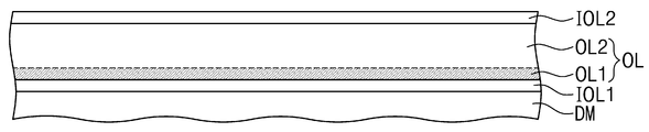
봉지 부재(EN)는 제1 무기층(IOL1), 제1 무기층(IOL1) 상에 배치되는 유기층(OL) 및 유기층(OL) 상에 배치되는 제2 무기층(IOL2)을 포함한다. 봉지 부재(EN)는 유기 발광 소자(OEL) 상에 배치되고, 유기 발광 소자(OEL)를 밀봉한다.The encapsulation member EN includes a first inorganic layer IOL1 , an organic layer OL disposed on the first inorganic layer IOL1 , and a second inorganic layer IOL2 disposed on the organic layer OL. The encapsulation member EN is disposed on the organic light emitting element OEL and encapsulates the organic light emitting element OEL.
제1 무기층(IOL1)은 표시 부재(DM) 상에 배치된다. 제1 무기층(IOL1)은 유기 발광 소자(OEL) 상에 배치된다. 구체적으로, 제1 무기층(IOL1)은 유기 발광 소자(OEL)의 제2 전극(EL2) 상에 접촉하여 배치될 수 있다. 제1 무기층(IOL1)은 유기 발광 소자(OEL) 및 화소 정의막(PDL)에 중첩하도록 배치될 수 있다. 제1 무기층(IOL1)은 무기물을 포함한다. 이에 한정되는 것은 아니나, 무기물은 예를 들어, 산화 알루미늄, 산화 실리콘, 질산화 실리콘, 질화 실리콘, 산화 아연, 산화 스트론튬, 산화 티타늄, 산화 하프늄 등을 포함할 수 있다. 제1 무기층(IOL1)은 유기 발광 소자(OEL)를 봉지하고, 유기 발광 소자(OEL)에 이물질이 유입되는 것을 방지하는 배리어막의 기능을 할 수 있다. 이하, 설명의 편의를 위해 제1 무기층(IOL1)은 제1 무기 봉지층(IOL1)으로 지칭한다.The first inorganic layer IOL1 is disposed on the display member DM. The first inorganic layer IOL1 is disposed on the organic light emitting element OEL. In detail, the first inorganic layer IOL1 may be disposed in contact with the second electrode EL2 of the organic light emitting diode OEL. The first inorganic layer IOL1 may be disposed to overlap the organic light emitting diode OEL and the pixel defining layer PDL. The first inorganic layer IOL1 includes an inorganic material. Although not limited thereto, the inorganic material may include, for example, aluminum oxide, silicon oxide, silicon nitride oxide, silicon nitride, zinc oxide, strontium oxide, titanium oxide, hafnium oxide, and the like. The first inorganic layer IOL1 may function as a barrier layer that encapsulates the organic light emitting element OEL and prevents foreign substances from being introduced into the organic light emitting element OEL. Hereinafter, for convenience of description, the first inorganic layer IOL1 is referred to as a first inorganic encapsulation layer IOL1 .
유기층(OL)은 제1 유기층(OL1) 및 제2 유기층(OL2)을 포함한다. 제1 유기층(OL1)은 단면 상에서 제1 무기 봉지층(IOL1)에 인접하게 배치된다. 제1 유기층(OL1)은 제1 무기 봉지층(IOL1) 상에 직접 배치된다. 제2 유기층(OL2)은 제1 유기층(OL1) 상에 배치된다. 제2 유기층(OL2)은 제1 유기층(OL1) 상에 직접 배치된다. 제2 유기층(OL2)은 제1 유기층(OL1)을 사이에 두고 제1 무기 봉지층(IOL1)과 이격되어 있을 수 있다. 유기층(OL)은 소정의 두께를 가지고, 유기 발광 소자(OEL)를 보호하는 보호막의 역할을 할 수도 있고, 상면을 평탄화시키는 평탄화막의 역할을 할 수도 있다.The organic layer OL includes a first organic layer OL1 and a second organic layer OL2 . The first organic layer OL1 is disposed adjacent to the first inorganic encapsulation layer IOL1 on a cross-section. The first organic layer OL1 is directly disposed on the first inorganic encapsulation layer IOL1 . The second organic layer OL2 is disposed on the first organic layer OL1 . The second organic layer OL2 is directly disposed on the first organic layer OL1 . The second organic layer OL2 may be spaced apart from the first inorganic encapsulation layer IOL1 with the first organic layer OL1 interposed therebetween. The organic layer OL has a predetermined thickness and may serve as a protective layer to protect the organic light emitting device OEL or as a planarization layer to planarize an upper surface of the organic layer OL.
제2 무기층(IOL2)은 유기층(OL) 상에 배치된다. 제2 무기층(IOL2)은 제2 유기층(OL2) 상에 직접 배치된다. 제2 무기층(IOL2)은 유기 발광 소자(OEL) 및 화소 정의막(PDL)에 중첩하도록 배치될 수 있다. 제2 무기층(IOL2)은 제1 무기 봉지층(IOL1)과 평면상에서 전면적으로 중첩할 수 있다. 제2 무기층(IOL2)은 무기물을 포함한다. 제2 무기층(IOL2)은 제1 무기 봉지층(IOL1)에 포함된 무기물과 동일한 무기물을 포함할 수 있다. 제2 무기층(IOL2)은 유기 발광 소자(OEL)를 봉지하고, 유기 발광 소자(OEL)에 이물질이 유입되는 것을 방지하는 배리어막의 기능을 할 수 있다. 이하, 설명의 편의를 위해 제2 무기층(IOL2)은 제2 무기 봉지층(IOL2)으로 지칭한다.The second inorganic layer IOL2 is disposed on the organic layer OL. The second inorganic layer IOL2 is directly disposed on the second organic layer OL2 . The second inorganic layer IOL2 may be disposed to overlap the organic light emitting element OEL and the pixel defining layer PDL. The second inorganic layer IOL2 may completely overlap the first inorganic encapsulation layer IOL1 in a plan view. The second inorganic layer IOL2 includes an inorganic material. The second inorganic layer IOL2 may include the same inorganic material as the inorganic material included in the first inorganic encapsulation layer IOL1 . The second inorganic layer IOL2 may function as a barrier layer that encapsulates the organic light emitting element OEL and prevents foreign substances from entering the organic light emitting element OEL. Hereinafter, for convenience of description, the second inorganic layer IOL2 is referred to as a second inorganic encapsulation layer IOL2 .
도 4a를 참조하면, 유기층(OL)은 제1 유기층(OL1) 및 제2 유기층(OL2)을 포함한다. 제1 유기층(OL1)은 단면상에서 제1 무기 봉지층(IOL1)에 인접하도록 배치된다. 제2 유기층(OL2)은 제1 유기층(OL1) 상에 배치되어, 단면상에서 제1 무기 봉지층(IOL1)과 이격될 수 있다. 제1 유기층(OL1)은 약 500Å 이상 약 4000Å 이하의 두께를 가질 수 있다.Referring to FIG. 4A , the organic layer OL includes a first organic layer OL1 and a second organic layer OL2 . The first organic layer OL1 is disposed adjacent to the first inorganic encapsulation layer IOL1 on a cross-section. The second organic layer OL2 may be disposed on the first organic layer OL1 to be spaced apart from the first inorganic encapsulation layer IOL1 in a cross-sectional view. The first organic layer OL1 may have a thickness of about 500 Å or more and about 4000 Å or less.
유기층(OL)은 실리콘계 유기 화합물을 포함한다. 유기층(OL)은 탄소(C) 및 규소(Si)를 포함하는 유기물을 포함한다. 유기층(OL)은 탄소, 규소 및 산소(O)를 포함하는 유기물을 포함할 수 있다. 유기층(OL)은 규소-산소 결합을 포함하는 실리콘계 화합물을 포함할 수 있다.The organic layer OL includes a silicon-based organic compound. The organic layer OL includes an organic material including carbon (C) and silicon (Si). The organic layer OL may include an organic material including carbon, silicon, and oxygen (O). The organic layer OL may include a silicon-based compound including a silicon-oxygen bond.
제1 유기층(OL1)의 규소 대비 탄소의 원자비는 제2 유기층(OL2)의 규소 대비 탄소의 원자비와 상이하다. 제1 유기층(OL1)의 규소 대비 탄소의 원자비는 제2 유기층(OL2)의 규소 대비 탄소의 원자비보다 낮다. 제1 유기층(OL1)은 제2 유기층(OL2)보다 탄소 함량이 낮고 탄소에 비해 규소 함량이 높은 것일 수 있다.The atomic ratio of carbon to silicon in the first organic layer OL1 is different from the atomic ratio of carbon to silicon in the second organic layer OL2 . The atomic ratio of carbon to silicon in the first organic layer OL1 is lower than the atomic ratio of carbon to silicon in the second organic layer OL2 . The first organic layer OL1 may have a lower carbon content than the second organic layer OL2 and a higher silicon content than carbon.
제1 유기층(OL1)의 규소 대비 탄소의 원자비는 약 1.24 미만일 수 있다. 보다 구체적으로, 제1 유기층(OL1)의 규소 대비 탄소의 원자비는 약 1.20 초과 약 1.24 미만일 수 있다. 제2 유기층(OL2)의 규소 대비 탄소의 원자비는 약 1.24 초과일 수 있다. 보다 구체적으로, 제2 유기층(OL2)의 규소 대비 탄소의 원자비는 약 1.24 초과 약 1.30 미만일 수 있다.The atomic ratio of carbon to silicon in the first organic layer OL1 may be less than about 1.24. More specifically, the atomic ratio of carbon to silicon in the first organic layer OL1 may be greater than about 1.20 and less than about 1.24. The atomic ratio of carbon to silicon in the second organic layer OL2 may be greater than about 1.24. More specifically, the atomic ratio of carbon to silicon of the second organic layer OL2 may be greater than about 1.24 and less than about 1.30.
제1 유기층(OL1)의 규소 대비 산소의 원자비는 제2 유기층(OL2)의 규소 대비 산소의 원자비와 상이할 수 있다. 제1 유기층(OL1)의 규소 대비 산소의 원자비는 제2 유기층(OL2)의 규소 대비 산소의 원자비보다 높을 수 있다. 제1 유기층(OL1)은 제2 유기층(OL2)보다 산소 함량이 낮고 산소에 비해 규소 함량이 높은 것일 수 있다.An atomic ratio of oxygen to silicon in the first organic layer OL1 may be different from an atomic ratio of oxygen to silicon in the second organic layer OL2 . An atomic ratio of oxygen to silicon in the first organic layer OL1 may be higher than an atomic ratio of oxygen to silicon in the second organic layer OL2 . The first organic layer OL1 may have a lower oxygen content than the second organic layer OL2 and a higher silicon content than oxygen.
제1 유기층(OL1)의 규소 대비 산소의 원자비는 약 0.62 초과일 수 있다. 보다 구체적으로, 제1 유기층(OL1)의 규소 대비 탄소의 원자비는 약 0.62 초과 약 0.64 미만일 수 있다. 제2 유기층(OL2)의 규소 대비 탄소의 원자비는 약 0.62 미만일 수 있다. 보다 구체적으로, 제2 유기층(OL2)의 규소 대비 탄소의 원자비는 약 0.60 초과 약 0.62 미만일 수 있다.The atomic ratio of oxygen to silicon in the first organic layer OL1 may be greater than about 0.62. More specifically, the atomic ratio of carbon to silicon in the first organic layer OL1 may be greater than about 0.62 and less than about 0.64. The atomic ratio of carbon to silicon in the second organic layer OL2 may be less than about 0.62. More specifically, the atomic ratio of carbon to silicon in the second organic layer OL2 may be greater than about 0.60 and less than about 0.62.
본 발명의 유기층(OL)은 규소 대비 탄소 및 산소 조성이 상이한 제1 유기층(OL1) 및 제2 유기층(OL2)을 포함한다. 제1 유기층(OL1)은 제2 유기층(OL2)에 비해 탄소의 함량이 적고 산소의 함량이 높아, 제2 유기층(OL2)에 비해 제1 무기 봉지층(IOL1)과 유사한 성질을 가질 수 있다. 제1 유기층(OL1)은 제2 유기층(OL2)에 비해 무기층에 가까운 성질을 가져, 제1 무기 봉지층(IOL1)과 접착력이 강할 수 있다.The organic layer OL of the present invention includes a first organic layer OL1 and a second organic layer OL2 having different carbon and oxygen compositions compared to silicon. The first organic layer OL1 may have a lower carbon content and a higher oxygen content than the second organic layer OL2 , and may have properties similar to those of the first inorganic encapsulation layer IOL1 compared to the second organic layer OL2 . The first organic layer OL1 may have a property closer to an inorganic layer than the second organic layer OL2 , and thus may have strong adhesion to the first inorganic encapsulation layer IOL1 .
본 발명의 유기층(OL)은 보다 무기층에 가까운 성질을 가지는 제1 유기층(OL1)을 제1 무기 봉지층(IOL1)에 인접하게 배치하여, 봉지 부재에서 제1 무기 봉지층(IOL1)과 유기층(OL) 사이의 접착력이 향상될 수 있다. 이에 따라, 봉지 부재의 안정성이 증가하여 표시 장치의 신뢰성이 향상될 수 있다.In the organic layer OL of the present invention, the first organic layer OL1 having a property closer to an inorganic layer is disposed adjacent to the first inorganic encapsulation layer IOL1, and the first inorganic encapsulation layer IOL1 and the organic layer are formed in the encapsulation member. The adhesion between (OL) can be improved. Accordingly, the stability of the encapsulation member may be increased, and thus the reliability of the display device may be improved.
도 4b를 참조하면, 본 발명의 유기층(OL)은 제1 유기층(OL1), 제2 유기층(OL2) 및 제1 유기층(OL1)과 제2 유기층(OL2) 사이에 배치되는 중간 유기층(OLC)을 포함할 수 있다. 중간 유기층(OLC)은 제1 유기층(OL1) 및 제2 유기층(OL2)의 규소 대비 탄소 원자비의 중간값을 가질 수 있다. 중간 유기층(OLC)은 제1 유기층(OL1) 및 제2 유기층(OL2)의 규소 대비 산소 원자비의 중간값을 가질 수 있다.Referring to FIG. 4B , the organic layer OL of the present invention includes a first organic layer OL1 , a second organic layer OL2 , and an intermediate organic layer OLC disposed between the first organic layer OL1 and the second organic layer OL2 . may include The intermediate organic layer OLC may have an intermediate value of a ratio of carbon atoms to silicon of the first organic layer OL1 and the second organic layer OL2 . The intermediate organic layer OLC may have an intermediate value of an atomic ratio of oxygen to silicon of the first organic layer OL1 and the second organic layer OL2 .
도 4a 및 도 4b에서, 제1 유기층(OL1)은 두께 방향을 따라 규소 대비 탄소 및 산소의 조성이 변화할 수 있다. 구체적으로, 제1 유기층(OL1)의 규소 대비 탄소의 원자비는 제2 유기층(OL2)에 인접할수록 증가하고, 제1 무기 봉지층(IOL1)에 인접할수록 감소할 수 있다. 제1 유기층(OL1)의 규소 대비 산소의 원자비는 제2 유기층(OL2)에 인접할수록 감소하고, 제1 무기 봉지층(IOL1)에 인접할수록 증가할 수 있다.4A and 4B , the composition of carbon and oxygen compared to silicon may change in the first organic layer OL1 along the thickness direction. Specifically, the atomic ratio of carbon to silicon of the first organic layer OL1 may increase as it approaches the second organic layer OL2 and may decrease as it approaches the first inorganic encapsulation layer IOL1 . The atomic ratio of oxygen to silicon of the first organic layer OL1 may decrease as it approaches the second organic layer OL2 and may increase as it approaches the first inorganic encapsulation layer IOL1 .
본 발명의 제1 유기층(OL1) 및 제2 유기층(OL2)은 연속 공정에 의해 형성될 수 있다. 이 때, 제1 유기층(OL1) 및 제2 유기층(OL2)의 규소 대비 탄소 및 산소의 조성을 달리하기 위하여, 공정 조건을 변화시켜 연속 공정을 진행할 수 있다. 연속 공정으로 형성할 때, 제1 유기층(OL1) 및 제2 유기층(OL2) 사이에는 제1 유기층(OL1)과 제2 유기층(OL2)의 중간 조성을 가지는 중간 유기층(OLC)이 형성될 수도 있다. 또는, 제1 유기층(OL1)을 형성하는 공정에서 공정 조건을 점진적으로 변화시켜, 제1 유기층(OL1)의 규소 대비 탄소 및 산소의 조성이 두께 방향을 따라 변화하는 것일 수도 있다.The first organic layer OL1 and the second organic layer OL2 of the present invention may be formed by a continuous process. In this case, in order to have different compositions of carbon and oxygen compared to silicon in the first organic layer OL1 and the second organic layer OL2 , a continuous process may be performed by changing process conditions. When formed by a continuous process, an intermediate organic layer OLC having an intermediate composition of the first organic layer OL1 and the second organic layer OL2 may be formed between the first organic layer OL1 and the second organic layer OL2 . Alternatively, the composition of carbon and oxygen relative to silicon of the first organic layer OL1 may be changed along the thickness direction by gradually changing process conditions in the process of forming the first organic layer OL1 .
이하에서는 본 발명의 일 실시예에 따른 표시 장치의 제조 방법에 대해서 설명한다.Hereinafter, a method of manufacturing a display device according to an exemplary embodiment of the present invention will be described.
도 5는 본 발명의 일 실시예에 따른 표시 장치의 제조 방법 중 일부 단계를 나타낸 순서도이다. 도 6a 내지 도 6f는 본 발명의 일 실시예에 따른 표시 장치의 제조 방법 중 일부 단계를 순차적으로 나타낸 단면도들이다.5 is a flowchart illustrating some steps of a method of manufacturing a display device according to an exemplary embodiment. 6A to 6F are cross-sectional views sequentially illustrating some steps of a method of manufacturing a display device according to an exemplary embodiment.
본 발명의 일 실시예에 따른 표시 장치의 제조 방법은 표시 부재를 준비하는 단계 및 표시 부재 상에 봉지 부재를 형성하는 단계를 포함한다. 본 발명의 표시 부재는 유기 발광 소자를 포함하고, 봉지 부재는 유기 발광 소자를 밀봉하도록 형성된다.A method of manufacturing a display device according to an exemplary embodiment includes preparing a display member and forming an encapsulation member on the display member. The display member of the present invention includes an organic light emitting device, and the encapsulation member is formed to encapsulate the organic light emitting device.
도 5에서는 본 발명의 본 발명의 일 실시예에 따른 봉지 부재를 형성하는 단계를 나타낸 순서도이다. 본 발명의 봉지 부재를 형성하는 단계는 제1 무기 봉지층(IOL1)을 형성하는 단계(S100), 유기층(OL)을 형성하는 단계(S200) 및 제2 무기 봉지 봉지층(IOL2)을 형성하는 단계(S300)를 포함한다.5 is a flowchart illustrating a step of forming an encapsulation member according to an embodiment of the present invention. The steps of forming the encapsulation member of the present invention include forming the first inorganic encapsulation layer (IOL1) (S100), forming the organic layer (OL) (S200), and forming the second inorganic encapsulation encapsulation layer (IOL2). Step S300 is included.
도 6a를 참조하면, 본 발명의 봉지 부재를 형성하는 단계는 표시 부재(DM)를 준비한 후, 표시 부재(DM) 상에 무기물을 증착하여 제1 무기 봉지층(IOL1)을 형성하는 단계(S100)를 포함한다. 이에 한정하는 것은 아니나, 제1 무기 봉지층(IOL1)은 화학 기상 증착법(CVD: Chemical Vapor Deposition)을 통해 형성될 수 있다.Referring to FIG. 6A , the step of forming the encapsulation member according to the present invention includes preparing the display member DM and then depositing an inorganic material on the display member DM to form the first inorganic encapsulation layer IOL1 ( S100 ). ) is included. Although not limited thereto, the first inorganic encapsulation layer IOL1 may be formed through chemical vapor deposition (CVD).
도 6b 내지 도 6e를 참조하면, 본 발명의 본 발명의 일 실시예에 따른 봉지 부재를 형성하는 단계는 제1 무기 봉지층(IOL1) 상에 유기층(OL)을 형성하는 단계(S200)를 포함한다. 유기층(OL)을 형성하는 단계(S200)는 제1 무기 봉지층(IOL1) 상에 유기물(OM)을 증착하여 제1 유기층(OL1)을 형성하는 단계, 및 제1 유기층(OL1) 상에 유기물(OM)을 증착하여 제2 유기층(OL2)을 형성하는 단계를 포함한다.6B to 6E , the step of forming the encapsulation member according to the exemplary embodiment of the present invention includes forming the organic layer OL on the first inorganic encapsulation layer IOL1 ( S200 ). do. Forming the organic layer OL ( S200 ) includes depositing an organic material OM on the first inorganic encapsulation layer IOL1 to form the first organic layer OL1 , and the organic material on the first organic layer OL1 . and depositing OM to form a second organic layer OL2 .
제1 유기층(OL1)은 제1 산소 분압(OP1) 하에서 유기물(OM)을 증착하여 제1 무기 봉지층(IOL1) 상에 형성된다. 유기물(OM)은 알콕시 실란계 화합물 또는 실록산계 화합물을 포함할 수 있다. 이에 한정되지 않으나, 유기물(OM)은 헥사메틸디실록산(Hexamethyldisiloxane; HMDSO), 테트라에틸오쏘실리케이트 (Tetraethyl orthosilicate; TEOS), 디에톡시메틸실란(Diethoxymethylsilane; DEMS), N-옥틸트리메톡시실란 (N-octyltrimethoxysilane; OCTMS) 중 적어도 어느 하나를 포함할 수 있다.The first organic layer OL1 is formed on the first inorganic encapsulation layer IOL1 by depositing the organic material OM under the first oxygen partial pressure OP1. The organic material (OM) may include an alkoxysilane-based compound or a siloxane-based compound. Although not limited thereto, the organic material (OM) is hexamethyldisiloxane (HMDSO), tetraethyl orthosilicate (TEOS), diethoxymethylsilane (DEMS), N-octyltrimethoxysilane (N -octyltrimethoxysilane; OCTMS) may be included.
제1 유기층(OL1)을 형성하는 단계에서, 유기물(OM)이 제1 산소 분압(OP1)에 의해 산화되는 반응이 포함될 수 있다. 구체적으로, 유기물(OM)이 전자 빔 등에 의해 분해된 후, 제1 산소 분압(OP1) 조건에서 산화될 수 있다.In the forming of the first organic layer OL1 , a reaction in which the organic material OM is oxidized by the first oxygen partial pressure OP1 may be included. Specifically, after the organic material OM is decomposed by an electron beam or the like, it may be oxidized under the first oxygen partial pressure OP1 condition.
제2 유기층(OL2)은 제2 산소 분압(OP2) 하에서 유기물(OM)을을 증착하여 제1 유기층(OL1) 상에 형성된다. 제2 유기층(OL2)을 형성하는 단계는 제1 유기층(OL1)을 형성하는 단계 이후에 연속 공정으로 이루어질 수 있다.The second organic layer OL2 is formed on the first organic layer OL1 by depositing the organic material OM under the second oxygen partial pressure OP2 . The forming of the second organic layer OL2 may be performed as a continuous process after the forming of the first organic layer OL1 .
제2 유기층(OL2)을 형성하는 단계에서 제공되는 유기물(OM)은 알콕시 실란계 화합물 또는 실록산계 화합물을 포함할 수 있다. 제2 유기층(OL2)을 형성하는 단계에서 제공되는 유기물(OM)은 제1 유기층(OL1)을 형성하는 단계에서 제공되는 유기물(OM)과 동일한 것일 수 있다. 제1 유기층(OL1)을 형성하는 단계 및 제2 유기층(OL2)을 형성하는 단계는 동일한 증착 물질을 이용하나, 산소 분압 등의 공정 조건을 달리하여 진행되는 것일 수 있다.The organic material OM provided in the step of forming the second organic layer OL2 may include an alkoxysilane-based compound or a siloxane-based compound. The organic material OM provided in the step of forming the second organic layer OL2 may be the same as the organic material OM provided in the step of forming the first organic layer OL1 . The forming of the first organic layer OL1 and the forming of the second organic layer OL2 may be performed by using the same deposition material but using different process conditions such as oxygen partial pressure.
제2 산소 분압(OP2)은 제1 산소 분압(OP1)보다 낮다. 제2 유기층(OL2)을 형성하는 단계에서, 유기물(OM)이 제2 산소 분압(OP2)에 의해 산화되는 반응이 포함될 수 있다. 제1 산소 분압(OP1)에 비해 제2 산소 분압(OP2)이 낮으므로, 제2 유기층(OL2)을 형성하는 단계에 비해 제1 유기층(OL1)을 형성하는 단계에서 유기물(OM)이 산화되는 비율이 높을 수 있다. 제1 유기층(OL1)을 형성하는 단계에서 더 많은 산화 반응이 이루어지므로, 제1 유기층(OL1)은 제2 유기층(OL2)에 비해 규소 대비 산소의 함량이 높고, 규소 대비 탄소의 함량은 상대적으로 낮은 것일 수 있다.The second oxygen partial pressure OP2 is lower than the first oxygen partial pressure OP1. In the forming of the second organic layer OL2 , a reaction in which the organic material OM is oxidized by the second oxygen partial pressure OP2 may be included. Since the second oxygen partial pressure OP2 is lower than the first oxygen partial pressure OP1, the organic material OM is oxidized in the step of forming the first organic layer OL1 compared to the step of forming the second organic layer OL2. ratio can be high. Since more oxidation reactions are performed in the step of forming the first organic layer OL1 , the first organic layer OL1 has a higher content of oxygen compared to silicon than that of the second organic layer OL2 , and the content of carbon compared to silicon is relatively higher than that of the second organic layer OL2 . may be low.
제1 유기층(OL1)을 형성하는 단계는 제1 산소 분압(OP1)을 변화시키며 이루어질 수 있다. 제1 유기층(OL1)을 형성하는 단계는 제1 산소 분압(OP1)을 점진적으로 감소시키며 이루어질 수 있다. 제1 산소 분압(OP1)을 점진적으로 감소시키며 제1 유기층(OL1)을 형성할 경우, 제1 유기층(OL1)은 두께 방향을 따라 규소 대비 탄소 및 산소의 조성이 변화할 수 있다. 구체적으로, 제1 유기층(OL1)의 규소 대비 탄소의 원자비는 제1 무기 봉지층(IOL1)에 인접할수록 감소할 수 있다. 제1 유기층(OL1)의 규소 대비 산소의 원자비는 제1 무기 봉지층(IOL1)에 인접할수록 증가할 수 있다.The forming of the first organic layer OL1 may be performed by changing the first oxygen partial pressure OP1. The forming of the first organic layer OL1 may be performed while gradually decreasing the first oxygen partial pressure OP1. When the first organic layer OL1 is formed while the first oxygen partial pressure OP1 is gradually decreased, the composition of carbon and oxygen relative to silicon may change along the thickness direction of the first organic layer OL1 . Specifically, the atomic ratio of carbon to silicon of the first organic layer OL1 may decrease as it is adjacent to the first inorganic encapsulation layer IOL1 . The atomic ratio of oxygen to silicon of the first organic layer OL1 may increase as it is adjacent to the first inorganic encapsulation layer IOL1 .
도 6f를 참조하면, 본 발명의 일 실시예에 따른 봉지 부재를 형성하는 단계는 유기층(OL) 상에 무기물을 증착하여 제2 무기 봉지층(IOL2)을 형성하는 단계(S300)를 포함한다. 이에 한정하는 것은 아니나, 제2 무기 봉지층(IOL2)은 화학 기상 증착법(CVD: Chemical Vapor Deposition)을 통해 형성될 수 있다.Referring to FIG. 6F , the step of forming the encapsulation member according to an embodiment of the present invention includes depositing an inorganic material on the organic layer OL to form the second inorganic encapsulation layer IOL2 ( S300 ). Although not limited thereto, the second inorganic encapsulation layer IOL2 may be formed through chemical vapor deposition (CVD).
본 발명의 일 실시예에 따른 표시 장치의 제조 방법에서, 제2 유기층(OL2)을 형성하는 단계는 제1 유기층(OL1)을 형성하는 단계 이후에 연속 공정으로 이루어질 수 있다. 제1 유기층(OL1)을 형성하는 단계 및 제2 유기층(OL2)을 형성하는 단계는 동일한 증착 물질을 이용하나, 산소 분압이나 전압 등의 공정 조건을 달리하여 진행되는 것일 수 있다. 본 발명의 일 실시예에 따른 표시 장치의 제조 방법은 연속 공정으로 조성이 다른 제1 유기층(OL1) 및 제2 유기층(OL2)을 형성함으로써, 공정 비용이 절감되고 단계가 간소화된 표시 장치의 제조 방법을 제공함과 동시에, 봉지 부재의 안정성이 향상되어 신뢰성이 향상된 표시 장치의 제조 방법을 제공할 수 있다.In the method of manufacturing the display device according to the exemplary embodiment, the forming of the second organic layer OL2 may be performed as a continuous process after the forming of the first organic layer OL1 . The forming of the first organic layer OL1 and the forming of the second organic layer OL2 may be performed using the same deposition material, but using different process conditions such as oxygen partial pressure or voltage. In the method of manufacturing a display device according to an exemplary embodiment of the present invention, by forming the first organic layer OL1 and the second organic layer OL2 having different compositions in a continuous process, the manufacturing cost of the display device is reduced and the steps are simplified. A method of manufacturing a display device having improved reliability by improving stability of an encapsulation member while providing a method may be provided.
이하에서는 본 발명의 구체적인 실험예를 통해 본 발명을 보다 구체적으로 설명한다. 하기 실시예는 본 발명의 이해를 돕기 위한 예시에 불과하며, 본 발명의 범위가 이에 한정되는 것은 아니다.Hereinafter, the present invention will be described in more detail through specific experimental examples of the present invention. The following examples are only examples to help the understanding of the present invention, and the scope of the present invention is not limited thereto.
도 7a는 본 발명의 제1 유기층의 원자 조성을 나타낸 그래프이다. 도 7b는 본 발명의 제2 유기층의 원자 조성을 나타낸 그래프이다. 도 7a 및 도 7b에서 나타난 데이터는 광전자분광기(XPS) 분석을 통해 측정하였다.7A is a graph showing the atomic composition of the first organic layer of the present invention. 7B is a graph showing the atomic composition of the second organic layer of the present invention. The data shown in FIGS. 7A and 7B were measured through photoelectron spectroscopy (XPS) analysis.
도 7a 및 도 7b에서 X축은 각 층의 두께를 나타내고, Y축은 원자 퍼센트를 나타낸다. 도 7a 및 도 7b를 참조하면, 본 발명의 제1 유기층 및 제2 유기층의 조성은 크게 차이가 없으나, 제1 유기층의 산소 원자 퍼센트가 높고, 제2 유기층의 탄소 원자 퍼센트가 높은 것을 확인할 수 있다.7A and 7B , the X-axis represents the thickness of each layer, and the Y-axis represents the atomic percent. 7A and 7B , the composition of the first organic layer and the second organic layer of the present invention is not significantly different, but it can be seen that the oxygen atom percentage of the first organic layer is high and the carbon atom percentage of the second organic layer is high. .
도 8a는 본 발명의 제1 유기층 및 제2 유기층의 규소 대비 산소 원자비율을 비교한 그래프이다. 도 8b는 본 발명의 제1 유기층 및 제2 유기층의 규소 대비 탄소 원자비율을 비교한 그래프이다.8A is a graph comparing oxygen atom ratios to silicon in a first organic layer and a second organic layer of the present invention. 8B is a graph comparing the ratio of carbon atoms to silicon in the first organic layer and the second organic layer of the present invention.
도 8a를 참조하면, 본 발명의 제1 유기층이 제2 유기층에 비해 규소 대비 산소 원자 비율이 높은 것을 확인할 수 있다. 비교적 낮은 두께(100nm)에서는 표면 산화 반응 등으로 인해 규소 대비 산소 원자의 비율이 유사하나, 내부로 갈수록 제1 유기층의 규소 대비 산소 비율이 제2 유기층에 비해 높은 것을 확인할 수 있다.Referring to FIG. 8A , it can be seen that the ratio of oxygen atoms to silicon is higher in the first organic layer of the present invention than in the second organic layer. At a relatively low thickness (100 nm), the ratio of oxygen atoms to silicon is similar due to a surface oxidation reaction, but it can be seen that the ratio of oxygen to silicon of the first organic layer is higher than that of the second organic layer toward the inside.
도 8b를 참조하면, 본 발명의 제1 유기층이 제2 유기층에 비해 규소 대비 탄소 원자 비율이 높은 것을 확인할 수 있다.Referring to FIG. 8B , it can be seen that the ratio of carbon atoms to silicon is higher in the first organic layer of the present invention than in the second organic layer.
도 9a는 본 발명의 제1 유기층 및 제2 유기층의 규소 대비 산소의 원자 비율 범위를 비교한 그래프이다. 도 9b는 본 발명의 제1 유기층 및 제2 유기층의 규소 대비 탄소의 원자 비율 범위를 비교한 그래프이다.9A is a graph comparing the atomic ratio ranges of oxygen to silicon in a first organic layer and a second organic layer of the present invention. 9B is a graph comparing the atomic ratio ranges of carbon to silicon in the first organic layer and the second organic layer of the present invention.
도 9a 및 도 9b를 참조하면, 본 발명의 제1 유기층의 규소 대비 산소 원자비는 약 0.62 초과 약 0.64 미만이다. 제1 유기층의 규소 대비 탄소 원자비는 약 1.20 초과 약 1.24 미만이다. 제2 유기층의 규소 대비 산소 원자비는 약 0.60 초과 약 0.62 미만이다. 제2 유기층의 규소 대비 탄소 원자비는 약 1.24 초과 약 1.30 미만이다.9A and 9B , the atomic ratio of oxygen to silicon in the first organic layer of the present invention is greater than about 0.62 and less than about 0.64. The atomic ratio of carbon to silicon in the first organic layer is greater than about 1.20 and less than about 1.24. The atomic ratio of oxygen to silicon in the second organic layer is greater than about 0.60 and less than about 0.62. The atomic ratio of carbon to silicon in the second organic layer is greater than about 1.24 and less than about 1.30.
본 발명의 일 실시예에 따른 제1 유기층 및 제2 유기층은 동일한 물질을 재료로 하여 형성하되, 산소 분압이나 전압 등의 공정 조건을 달리하여 형성하므로, 규소 대비 산소 및 탄소의 원자비가 큰 차이를 보이지는 않으나, 제1 유기층은 제2 유기층에 비해 산소 원자의 비율이 높고, 탄소 원자의 비율이 낮다.The first organic layer and the second organic layer according to an embodiment of the present invention are formed using the same material as a material, but are formed under different process conditions such as oxygen partial pressure and voltage, so that a large difference in the atomic ratio of oxygen and carbon to silicon Although not visible, the ratio of oxygen atoms is higher in the first organic layer and the ratio of carbon atoms is lower than those of the second organic layer.
도 10a는 본 발명의 일 실시예에 따른 표시 장치로 표면 스크래치 시험을 진행한 시험 결과로, 봉지 부재에 제1 무기 봉지층, 제1 유기층, 제2 유기층. 제2 무기 봉지층 순서로 적층된 표시 장치로 시험한 것이다. 도 10b는 비교예에 따른 표시 장치로 표면 스크래치 시험을 진행한 시험 결과로, 본 발명의 제1 유기층에 대응하는 구성이 없는 것을 제외하고는 본 발명 시험예와 동일하게 적층된 표시 장치로 시험한 것이다.10A is a result of a surface scratch test performed on a display device according to an embodiment of the present invention, and a first inorganic encapsulation layer, a first organic layer, and a second organic layer are formed on the encapsulation member; It was tested with a display device stacked in the order of the second inorganic encapsulation layer. 10B is a test result of a surface scratch test performed with a display device according to a comparative example, and is a display device stacked in the same manner as in Test Example of the present invention except that there is no configuration corresponding to the first organic layer of the present invention. will be.
도 10a 및 도 10b를 참조하면, 스크래치 시험 결과 비교예의 경우 스크래치에 의해 표면이 박리된 부분의 영역이 본 발명 시험예에 비해 넓은 것을 확인할 수 있다. 본 발명에서는 규소 대비 산소의 조성이 보다 높은 제1 유기층을 더 포함하여, 봉지 부재에서 무기층과 유기층 사이의 접착력이 향상되므로, 외부 스크래치 등에 의한 표시 장치의 불량이 방지되고, 안정성 및 신뢰성이 향상된 표시 장치를 제공할 수 있음을 확인하였다.Referring to FIGS. 10A and 10B , it can be seen that, in the case of the comparative example of the scratch test, the area of the portion where the surface is peeled off by the scratch is wider than that of the test example of the present invention. In the present invention, since the first organic layer having a higher oxygen composition than silicon is further included, adhesion between the inorganic layer and the organic layer in the encapsulation member is improved, so that defects in the display device due to external scratches are prevented, and stability and reliability are improved It was confirmed that a display device can be provided.
이상에서는 본 발명의 바람직한 실시예를 참조하여 설명하였지만, 해당 기술 분야의 숙련된 당업자 또는 해당 기술 분야에 통상의 지식을 갖는 자라면, 후술될 특허청구범위에 기재된 본 발명의 사상 및 기술 영역으로부터 벗어나지 않는 범위 내에서 본 발명을 다양하게 수정 및 변경시킬 수 있음을 이해할 수 있을 것이다. 따라서, 본 발명의 기술적 범위는 명세서의 상세한 설명에 기재된 내용으로 한정되는 것이 아니라 특허청구범위에 의해 정하여져야만 할 것이다.Although the above has been described with reference to the preferred embodiment of the present invention, those skilled in the art or those with ordinary skill in the art will not depart from the spirit and scope of the present invention described in the claims to be described later. It will be understood that various modifications and variations of the present invention can be made without departing from the scope of the present invention. Accordingly, the technical scope of the present invention should not be limited to the contents described in the detailed description of the specification, but should be defined by the claims.
DD: 표시 장치 DM: 표시 부재
EN: 봉지 부재 OL: 유기층
OL1: 제1 유기층 OL2: 제2 유기층
IOL1: 제1 무기 봉지층 IOL2: 제2 무기 봉지층DD: display device DM: display member
EN: Encapsulation member OL: Organic layer
OL1: first organic layer OL2: second organic layer
IOL1: first inorganic encapsulation layer IOL2: second inorganic encapsulation layer
Claims (17)
상기 유기 발광 소자 상에 배치되고, 상기 유기 발광 소자를 밀봉하는 봉지 부재를 포함하고,
상기 봉지 부재는
상기 유기 발광 소자 상에 배치된 제1 무기 봉지층;
상기 제1 무기 봉지층 상에 배치된 제1 유기층 및 상기 제1 유기층 상에 배치된 제2 유기층을 포함하는 유기층; 및
상기 유기층 상에 배치된 제2 무기 봉지층을 포함하고,
상기 제1 유기층의 규소(Si) 대비 탄소(C)의 원자비는 상기 제2 유기층의 규소 대비 탄소의 원자비보다 낮고,
상기 제1 유기층의 일면은 상기 제1 무기 봉지층에 접촉하고, 상기 제1 유기층의 타면은 상기 제2 유기층에 접촉하고,
상기 제2 유기층의 일면은 상기 제1 유기층에 접촉하고, 상기 제2 유기층의 타면은 상기 제2 무기 봉지층에 접촉하는 표시 장치.organic light emitting device; and
an encapsulation member disposed on the organic light emitting device and sealing the organic light emitting device;
The sealing member is
a first inorganic encapsulation layer disposed on the organic light emitting device;
an organic layer including a first organic layer disposed on the first inorganic encapsulation layer and a second organic layer disposed on the first organic layer; and
a second inorganic encapsulation layer disposed on the organic layer;
The atomic ratio of carbon (C) to silicon (Si) of the first organic layer is lower than the atomic ratio of silicon to carbon in the second organic layer,
One surface of the first organic layer is in contact with the first inorganic encapsulation layer, and the other surface of the first organic layer is in contact with the second organic layer,
One surface of the second organic layer is in contact with the first organic layer, and the other surface of the second organic layer is in contact with the second inorganic encapsulation layer.
상기 제1 유기층의 규소 대비 탄소의 원자비는 1.24 미만인 표시 장치.According to claim 1,
and an atomic ratio of carbon to silicon in the first organic layer is less than 1.24.
상기 제1 유기층의 규소 대비 탄소의 원자비는 1.20 초과이고,
상기 제2 유기층의 규소 대비 탄소의 원자비는 1.30 미만인 표시 장치.3. The method of claim 2,
The atomic ratio of carbon to silicon in the first organic layer is greater than 1.20,
and an atomic ratio of carbon to silicon in the second organic layer is less than 1.30.
상기 유기층은 규소(Si)-산소(O) 결합을 포함하는 실리콘계 화합물을 포함하는 표시 장치.According to claim 1,
The organic layer includes a silicon-based compound including a silicon (Si)-oxygen (O) bond.
상기 제1 유기층의 규소 대비 산소의 원자비는 상기 제2 유기층의 규소 대비 산소의 원자비보다 높은 표시 장치.5. The method of claim 4,
An atomic ratio of oxygen to silicon in the first organic layer is higher than an atomic ratio of oxygen to silicon in the second organic layer.
상기 제1 유기층의 규소 대비 산소의 원자비는 0.62 초과인 표시 장치.6. The method of claim 5,
and an atomic ratio of oxygen to silicon in the first organic layer is greater than 0.62.
상기 제1 유기층의 규소 대비 산소의 원자비는 0.64 미만이고,
상기 제2 유기층의 규소 대비 산소의 원자비는 0.60 초과인 표시 장치.7. The method of claim 6,
The atomic ratio of oxygen to silicon in the first organic layer is less than 0.64,
and an atomic ratio of oxygen to silicon in the second organic layer is greater than 0.60.
상기 제1 유기층의 규소 대비 탄소의 원자비는
상기 제2 유기층에 인접할수록 증가하는 표시 장치.According to claim 1,
The atomic ratio of carbon to silicon in the first organic layer
The display device increases in proximity to the second organic layer.
상기 제1 유기층의 규소 대비 산소의 원자비는
상기 제1 무기 봉지층에 인접할수록 증가하는 표시 장치.5. The method of claim 4,
The atomic ratio of oxygen to silicon in the first organic layer
The display device increases in proximity to the first inorganic encapsulation layer.
상기 유기 발광 소자를 밀봉하도록 봉지 부재를 형성하는 단계를 포함하고,
상기 봉지 부재를 형성하는 단계는
상기 유기 발광 소자 상에 무기물을 증착하여 제1 무기 봉지층을 형성하는 단계;
상기 제1 무기 봉지층 상에 유기층을 형성하는 단계; 및
상기 유기층 상에 무기물을 증착하여 제2 무기 봉지층을 형성하는 단계를 포함하고,
상기 유기층을 형성하는 단계는
제1 산소 분압 하에서 상기 제1 무기 봉지층 상에 유기물을 증착하여 제1 유기층을 형성하는 단계; 및
상기 제1 산소 분압보다 낮은 제2 산소 분압 하에서 상기 제1 유기층 상에 유기물을 증착하여 제2 유기층을 형성하는 단계를 포함하고,
상기 제1 유기층의 일면은 상기 제1 무기 봉지층에 접촉하고, 상기 제1 유기층의 타면은 상기 제2 유기층에 접촉하고,
상기 제2 유기층의 일면은 상기 제1 유기층에 접촉하고, 상기 제2 유기층의 타면은 상기 제2 무기 봉지층에 접촉하는 표시 장치의 제조 방법.preparing an organic light emitting device; and
forming an encapsulation member to seal the organic light emitting diode;
The step of forming the encapsulation member is
depositing an inorganic material on the organic light emitting device to form a first inorganic encapsulation layer;
forming an organic layer on the first inorganic encapsulation layer; and
depositing an inorganic material on the organic layer to form a second inorganic encapsulation layer;
The step of forming the organic layer is
forming a first organic layer by depositing an organic material on the first inorganic encapsulation layer under a first oxygen partial pressure; and
forming a second organic layer by depositing an organic material on the first organic layer under a second oxygen partial pressure lower than the first oxygen partial pressure;
One surface of the first organic layer is in contact with the first inorganic encapsulation layer, and the other surface of the first organic layer is in contact with the second organic layer,
One surface of the second organic layer is in contact with the first organic layer, and the other surface of the second organic layer is in contact with the second inorganic encapsulation layer.
상기 유기층을 형성하는 단계에서 상기 유기물은 소정의 산소 분압 하에서 산화되고,
상기 제2 유기층을 형성하는 단계에 비해 상기 제1 유기층을 형성하는 단계에서 유기물이 산화되는 비율이 높은 표시 장치의 제조 방법.11. The method of claim 10,
In the step of forming the organic layer, the organic material is oxidized under a predetermined oxygen partial pressure,
A method of manufacturing a display device in which an organic material is oxidized at a higher rate in forming the first organic layer than in forming the second organic layer.
상기 제1 유기층을 형성하는 단계 및 상기 제2 유기층을 형성하는 단계는
연속 공정으로 이루어지는 표시 장치의 제조 방법.11. The method of claim 10,
The step of forming the first organic layer and the step of forming the second organic layer are
A method of manufacturing a display device comprising a continuous process.
상기 제1 유기층을 형성하는 단계는
상기 제1 산소 분압을 점진적으로 감소시키며 이루어지는 표시 장치의 제조 방법.13. The method of claim 12,
The step of forming the first organic layer is
A method of manufacturing a display device comprising gradually decreasing the first oxygen partial pressure.
상기 유기물은 알콕시 실란계 화합물 또는 실록산계 화합물을 포함하는 표시 장치의 제조 방법.11. The method of claim 10,
wherein the organic material includes an alkoxysilane-based compound or a siloxane-based compound.
상기 제1 유기층 및 상기 제2 유기층은 동일한 유기물로 형성되는 표시 장치의 제조 방법.15. The method of claim 14,
The method of manufacturing a display device, wherein the first organic layer and the second organic layer are formed of the same organic material.
상기 유기 발광 소자 상에 배치되고, 상기 유기 발광 소자를 밀봉하는 봉지 부재를 포함하고,
상기 봉지 부재는
상기 유기 발광 소자 상에 배치된 제1 무기 봉지층;
상기 제1 무기 봉지층 상에 배치된 제1 유기층, 상기 제1 유기층 상에 배치된 중간 유기층, 및 상기 중간 유기층 상에 배치된 제2 유기층을 포함하는 유기층; 및
상기 유기층 상에 배치된 제2 무기 봉지층을 포함하고,
상기 제1 유기층의 규소(Si) 대비 탄소(C)의 원자비는 상기 제2 유기층의 규소 대비 탄소의 원자비보다 낮고,
상기 중간 유기층의 규소 대비 탄소의 원자비는 상기 제1 유기층의 규소 대비 산소 원자비 및 상기 제2 유기층의 규소 대비 산소 원자비의 중간값을 가지고,
상기 제1 유기층의 일면은 상기 제1 무기 봉지층에 접촉하고, 상기 제1 유기층의 타면은 상기 중간 유기층에 접촉하고,
상기 중간 유기층의 일면은 상기 제1 유기층에 접촉하고, 상기 중간 유기층의 타면은 상기 제2 유기층에 접촉하고,
상기 제2 유기층의 일면은 상기 중간 유기층에 접촉하고, 상기 제2 유기층의 타면은 상기 제2 무기 봉지층에 접촉하는 표시 장치.
organic light emitting device; and
an encapsulation member disposed on the organic light emitting device and sealing the organic light emitting device;
The sealing member is
a first inorganic encapsulation layer disposed on the organic light emitting device;
an organic layer including a first organic layer disposed on the first inorganic encapsulation layer, an intermediate organic layer disposed on the first organic layer, and a second organic layer disposed on the intermediate organic layer; and
a second inorganic encapsulation layer disposed on the organic layer;
The atomic ratio of carbon (C) to silicon (Si) in the first organic layer is lower than the atomic ratio of carbon to silicon in the second organic layer,
The atomic ratio of carbon to silicon in the intermediate organic layer has a median value between the atomic ratio of oxygen to silicon in the first organic layer and the atomic ratio of oxygen to silicon in the second organic layer,
One surface of the first organic layer is in contact with the first inorganic encapsulation layer, and the other surface of the first organic layer is in contact with the intermediate organic layer,
One surface of the intermediate organic layer is in contact with the first organic layer, and the other surface of the intermediate organic layer is in contact with the second organic layer,
One surface of the second organic layer is in contact with the intermediate organic layer, and the other surface of the second organic layer is in contact with the second inorganic encapsulation layer.
Priority Applications (3)
| Application Number | Priority Date | Filing Date | Title |
|---|---|---|---|
| KR1020170043117A KR102343390B1 (en) | 2017-04-03 | 2017-04-03 | Display device and manufacturing method of the same |
| US15/846,015 US10529940B2 (en) | 2017-04-03 | 2017-12-18 | Display device with encapsulation layer with varying ratios of carbon to silicon and oxygen to silicon and method of fabricating the same |
| US16/703,593 US10873046B2 (en) | 2017-04-03 | 2019-12-04 | Display device with encapsulation layer with varying ratios of carbon to silicon and oxygen to silicon and method of fabricating the same |
Applications Claiming Priority (1)
| Application Number | Priority Date | Filing Date | Title |
|---|---|---|---|
| KR1020170043117A KR102343390B1 (en) | 2017-04-03 | 2017-04-03 | Display device and manufacturing method of the same |
Publications (2)
| Publication Number | Publication Date |
|---|---|
| KR20180112895A KR20180112895A (en) | 2018-10-15 |
| KR102343390B1 true KR102343390B1 (en) | 2021-12-28 |
Family
ID=63670931
Family Applications (1)
| Application Number | Title | Priority Date | Filing Date |
|---|---|---|---|
| KR1020170043117A Active KR102343390B1 (en) | 2017-04-03 | 2017-04-03 | Display device and manufacturing method of the same |
Country Status (2)
| Country | Link |
|---|---|
| US (2) | US10529940B2 (en) |
| KR (1) | KR102343390B1 (en) |
Cited By (1)
| Publication number | Priority date | Publication date | Assignee | Title |
|---|---|---|---|---|
| US12514058B2 (en) | 2022-08-19 | 2025-12-30 | Samsung Display Co., Ltd. | Display device |
Families Citing this family (3)
| Publication number | Priority date | Publication date | Assignee | Title |
|---|---|---|---|---|
| KR102343390B1 (en) | 2017-04-03 | 2021-12-28 | 삼성디스플레이 주식회사 | Display device and manufacturing method of the same |
| CN110459565A (en) * | 2019-08-01 | 2019-11-15 | 武汉华星光电半导体显示技术有限公司 | Display panel and method of making the same |
| CN110453175B (en) * | 2019-08-22 | 2021-08-03 | 中国科学院微电子研究所 | A kind of preparation method of vanadium oxide film |
Citations (4)
| Publication number | Priority date | Publication date | Assignee | Title |
|---|---|---|---|---|
| US20030164496A1 (en) | 2002-02-27 | 2003-09-04 | Samsung Sdi Co., Ltd. | Organic electroluminescent display device and method of manufacturing the same |
| US20060006778A1 (en) | 2004-06-26 | 2006-01-12 | Joon-Gu Lee | Organic electroluminescent display device and method for manufacturing the same |
| US20090297813A1 (en) | 2004-06-30 | 2009-12-03 | General Electric Company | System and method for making a graded barrier coating |
| US20140027722A1 (en) | 2012-07-24 | 2014-01-30 | Samsung Display Co. Ltd. | Organic light-emitting display apparatus and method of manufacturing the same |
Family Cites Families (21)
| Publication number | Priority date | Publication date | Assignee | Title |
|---|---|---|---|---|
| KR100493322B1 (en) | 2003-01-06 | 2005-06-07 | 엘지전자 주식회사 | multi protection layer of organic electroluminescence device and method of the same |
| US20060158101A1 (en) * | 2003-03-04 | 2006-07-20 | Dow Corning Corporation | Organic light-emitting diode |
| US20090029781A1 (en) * | 2005-08-24 | 2009-01-29 | Ayers Gear And Machine, Inc. | Greasable cv-joint wheel hub |
| JP4745181B2 (en) * | 2006-09-26 | 2011-08-10 | 富士フイルム株式会社 | ORGANIC EL LIGHT EMITTING DEVICE AND METHOD FOR MANUFACTURING ORGANIC EL LIGHT EMITTING DEVICE |
| KR101560234B1 (en) | 2009-06-29 | 2015-10-15 | 엘지디스플레이 주식회사 | Organic Light Emitting Display Device and Method for fabricating the same |
| TWI577066B (en) | 2011-02-08 | 2017-04-01 | 應用材料股份有限公司 | Hybrid packaging method of organic light emitting diode |
| KR20120119768A (en) | 2011-04-22 | 2012-10-31 | 삼성디스플레이 주식회사 | Organic light emitting diode display and method for manufacturing organic light emitting diode display |
| TWI501873B (en) | 2011-12-27 | 2015-10-01 | Nitto Denko Corp | Transparent gas barrier film, transparent gas barrier film manufacturing method, organic EL element, solar cell and thin film battery |
| KR101889013B1 (en) * | 2012-05-17 | 2018-08-21 | 삼성디스플레이 주식회사 | Thin film encapsulation for a flat display device and the manufacturing method thereof |
| US9449809B2 (en) | 2012-07-20 | 2016-09-20 | Applied Materials, Inc. | Interface adhesion improvement method |
| US9397318B2 (en) | 2012-09-04 | 2016-07-19 | Applied Materials, Inc. | Method for hybrid encapsulation of an organic light emitting diode |
| KR20140087470A (en) | 2012-12-31 | 2014-07-09 | 주식회사 테스 | Deposition method of passivation film for light emitting diode |
| US9331311B2 (en) | 2013-03-04 | 2016-05-03 | Applied Materials, Inc. | Fluorine-containing plasma polymerized HMDSO for OLED thin film encapsulation |
| KR101780019B1 (en) | 2013-03-11 | 2017-09-19 | 어플라이드 머티어리얼스, 인코포레이티드 | Plasma curing of pecvd hmdso film for oled applications |
| KR102088203B1 (en) | 2013-10-01 | 2020-03-12 | 엘지디스플레이 주식회사 | Organic light emitting diode display and manufacturing method thereof |
| KR20150044723A (en) * | 2013-10-17 | 2015-04-27 | 삼성디스플레이 주식회사 | An organic light emtting device and a method for preparing the same |
| EP3002799B1 (en) | 2014-09-30 | 2023-09-13 | LG Display Co., Ltd. | Flexible organic light emitting display device |
| KR102327834B1 (en) | 2014-11-30 | 2021-11-17 | 엘지디스플레이 주식회사 | Flexible organic light emitting display apparatus |
| KR102298757B1 (en) | 2014-10-24 | 2021-09-07 | 삼성디스플레이 주식회사 | Organic light emitting diode device |
| KR101877402B1 (en) * | 2015-02-24 | 2018-07-13 | 에이피시스템 주식회사 | Passivation film for organic electronic devices and Method for depositing the same |
| KR102343390B1 (en) | 2017-04-03 | 2021-12-28 | 삼성디스플레이 주식회사 | Display device and manufacturing method of the same |
-
2017
- 2017-04-03 KR KR1020170043117A patent/KR102343390B1/en active Active
- 2017-12-18 US US15/846,015 patent/US10529940B2/en active Active
-
2019
- 2019-12-04 US US16/703,593 patent/US10873046B2/en active Active
Patent Citations (4)
| Publication number | Priority date | Publication date | Assignee | Title |
|---|---|---|---|---|
| US20030164496A1 (en) | 2002-02-27 | 2003-09-04 | Samsung Sdi Co., Ltd. | Organic electroluminescent display device and method of manufacturing the same |
| US20060006778A1 (en) | 2004-06-26 | 2006-01-12 | Joon-Gu Lee | Organic electroluminescent display device and method for manufacturing the same |
| US20090297813A1 (en) | 2004-06-30 | 2009-12-03 | General Electric Company | System and method for making a graded barrier coating |
| US20140027722A1 (en) | 2012-07-24 | 2014-01-30 | Samsung Display Co. Ltd. | Organic light-emitting display apparatus and method of manufacturing the same |
Cited By (1)
| Publication number | Priority date | Publication date | Assignee | Title |
|---|---|---|---|---|
| US12514058B2 (en) | 2022-08-19 | 2025-12-30 | Samsung Display Co., Ltd. | Display device |
Also Published As
| Publication number | Publication date |
|---|---|
| US20180287085A1 (en) | 2018-10-04 |
| US20200119301A1 (en) | 2020-04-16 |
| US10873046B2 (en) | 2020-12-22 |
| KR20180112895A (en) | 2018-10-15 |
| US10529940B2 (en) | 2020-01-07 |
Similar Documents
| Publication | Publication Date | Title |
|---|---|---|
| KR102668191B1 (en) | Organic light emitting display device | |
| KR102778471B1 (en) | Display apparatus and the manufacturing method thereof | |
| US10418588B2 (en) | Display device and organic luminescent display device | |
| KR102866753B1 (en) | Display device | |
| KR102248641B1 (en) | Organic electro luminescent device | |
| US8748931B2 (en) | Organic light emitting display apparatus including a filler and method of manufacturing the same | |
| US20180026087A1 (en) | Organic light-emitting display apparatus | |
| KR102486987B1 (en) | Organic light emitting diode display | |
| US11877477B2 (en) | Organic light-emitting display apparatus | |
| EP3790067B1 (en) | Display apparatus | |
| KR20180061866A (en) | Encapsulation unit and organic light emitting display including the same | |
| US20090298209A1 (en) | Optoelectronic device manufacturing | |
| US10873046B2 (en) | Display device with encapsulation layer with varying ratios of carbon to silicon and oxygen to silicon and method of fabricating the same | |
| KR20210113487A (en) | display apparatus | |
| KR20160035733A (en) | Organic light emitting display device and method of manufacturing the same | |
| TW201637257A (en) | Transparent organic light emitting display device | |
| KR101957145B1 (en) | Organic Light Emitting diode display and method of manufacturing the same | |
| US12063817B2 (en) | Display apparatus and method of manufacturing the same | |
| CN101765869A (en) | Display device and method for manufacturing display device | |
| CN113013198A (en) | Display device comprising a see-through area for a camera | |
| US9461270B2 (en) | Method for manufacturing organic light emitting diode display device | |
| KR20150131428A (en) | Organic electroluminescent device and method for fabricating the same | |
| US20240341123A1 (en) | Display device | |
| US20240065080A1 (en) | Display device | |
| CN112563435B (en) | display panel |
Legal Events
| Date | Code | Title | Description |
|---|---|---|---|
| PA0109 | Patent application |
St.27 status event code: A-0-1-A10-A12-nap-PA0109 |
|
| PG1501 | Laying open of application |
St.27 status event code: A-1-1-Q10-Q12-nap-PG1501 |
|
| R18-X000 | Changes to party contact information recorded |
St.27 status event code: A-3-3-R10-R18-oth-X000 |
|
| A201 | Request for examination | ||
| PA0201 | Request for examination |
St.27 status event code: A-1-2-D10-D11-exm-PA0201 |
|
| D13-X000 | Search requested |
St.27 status event code: A-1-2-D10-D13-srh-X000 |
|
| D14-X000 | Search report completed |
St.27 status event code: A-1-2-D10-D14-srh-X000 |
|
| E902 | Notification of reason for refusal | ||
| PE0902 | Notice of grounds for rejection |
St.27 status event code: A-1-2-D10-D21-exm-PE0902 |
|
| E13-X000 | Pre-grant limitation requested |
St.27 status event code: A-2-3-E10-E13-lim-X000 |
|
| P11-X000 | Amendment of application requested |
St.27 status event code: A-2-2-P10-P11-nap-X000 |
|
| P13-X000 | Application amended |
St.27 status event code: A-2-2-P10-P13-nap-X000 |
|
| E701 | Decision to grant or registration of patent right | ||
| PE0701 | Decision of registration |
St.27 status event code: A-1-2-D10-D22-exm-PE0701 |
|
| GRNT | Written decision to grant | ||
| PR0701 | Registration of establishment |
St.27 status event code: A-2-4-F10-F11-exm-PR0701 |
|
| PR1002 | Payment of registration fee |
St.27 status event code: A-2-2-U10-U11-oth-PR1002 Fee payment year number: 1 |
|
| PG1601 | Publication of registration |
St.27 status event code: A-4-4-Q10-Q13-nap-PG1601 |
|
| P22-X000 | Classification modified |
St.27 status event code: A-4-4-P10-P22-nap-X000 |
|
| P22-X000 | Classification modified |
St.27 status event code: A-4-4-P10-P22-nap-X000 |
|
| PR1001 | Payment of annual fee |
St.27 status event code: A-4-4-U10-U11-oth-PR1001 Fee payment year number: 4 |
|
| P22-X000 | Classification modified |
St.27 status event code: A-4-4-P10-P22-nap-X000 |