KR102314137B1 - Non-volatile Memory Device performing selective recovery operation and Operating Method thereof - Google Patents
Non-volatile Memory Device performing selective recovery operation and Operating Method thereof Download PDFInfo
- Publication number
- KR102314137B1 KR102314137B1 KR1020150154771A KR20150154771A KR102314137B1 KR 102314137 B1 KR102314137 B1 KR 102314137B1 KR 1020150154771 A KR1020150154771 A KR 1020150154771A KR 20150154771 A KR20150154771 A KR 20150154771A KR 102314137 B1 KR102314137 B1 KR 102314137B1
- Authority
- KR
- South Korea
- Prior art keywords
- memory
- recovery
- command
- read command
- read
- Prior art date
- Legal status (The legal status is an assumption and is not a legal conclusion. Google has not performed a legal analysis and makes no representation as to the accuracy of the status listed.)
- Active
Links
Images


Classifications
-
- G—PHYSICS
- G11—INFORMATION STORAGE
- G11C—STATIC STORES
- G11C11/00—Digital stores characterised by the use of particular electric or magnetic storage elements; Storage elements therefor
- G11C11/56—Digital stores characterised by the use of particular electric or magnetic storage elements; Storage elements therefor using storage elements with more than two stable states represented by steps, e.g. of voltage, current, phase, frequency
- G11C11/5621—Digital stores characterised by the use of particular electric or magnetic storage elements; Storage elements therefor using storage elements with more than two stable states represented by steps, e.g. of voltage, current, phase, frequency using charge storage in a floating gate
- G11C11/5642—Sensing or reading circuits; Data output circuits
-
- G—PHYSICS
- G11—INFORMATION STORAGE
- G11C—STATIC STORES
- G11C16/00—Erasable programmable read-only memories
- G11C16/02—Erasable programmable read-only memories electrically programmable
- G11C16/06—Auxiliary circuits, e.g. for writing into memory
- G11C16/26—Sensing or reading circuits; Data output circuits
-
- G—PHYSICS
- G11—INFORMATION STORAGE
- G11C—STATIC STORES
- G11C16/00—Erasable programmable read-only memories
- G11C16/02—Erasable programmable read-only memories electrically programmable
- G11C16/06—Auxiliary circuits, e.g. for writing into memory
- G11C16/10—Programming or data input circuits
- G11C16/20—Initialising; Data preset; Chip identification
-
- G—PHYSICS
- G11—INFORMATION STORAGE
- G11C—STATIC STORES
- G11C11/00—Digital stores characterised by the use of particular electric or magnetic storage elements; Storage elements therefor
- G11C11/56—Digital stores characterised by the use of particular electric or magnetic storage elements; Storage elements therefor using storage elements with more than two stable states represented by steps, e.g. of voltage, current, phase, frequency
- G11C11/5621—Digital stores characterised by the use of particular electric or magnetic storage elements; Storage elements therefor using storage elements with more than two stable states represented by steps, e.g. of voltage, current, phase, frequency using charge storage in a floating gate
- G11C11/5628—Programming or writing circuits; Data input circuits
-
- G—PHYSICS
- G11—INFORMATION STORAGE
- G11C—STATIC STORES
- G11C16/00—Erasable programmable read-only memories
- G11C16/02—Erasable programmable read-only memories electrically programmable
- G11C16/06—Auxiliary circuits, e.g. for writing into memory
- G11C16/08—Address circuits; Decoders; Word-line control circuits
-
- G—PHYSICS
- G11—INFORMATION STORAGE
- G11C—STATIC STORES
- G11C16/00—Erasable programmable read-only memories
- G11C16/02—Erasable programmable read-only memories electrically programmable
- G11C16/06—Auxiliary circuits, e.g. for writing into memory
- G11C16/10—Programming or data input circuits
-
- G—PHYSICS
- G11—INFORMATION STORAGE
- G11C—STATIC STORES
- G11C16/00—Erasable programmable read-only memories
- G11C16/02—Erasable programmable read-only memories electrically programmable
- G11C16/06—Auxiliary circuits, e.g. for writing into memory
- G11C16/34—Determination of programming status, e.g. threshold voltage, overprogramming or underprogramming, retention
- G11C16/3404—Convergence or correction of memory cell threshold voltages; Repair or recovery of overerased or overprogrammed cells
-
- G—PHYSICS
- G11—INFORMATION STORAGE
- G11C—STATIC STORES
- G11C29/00—Checking stores for correct operation ; Subsequent repair; Testing stores during standby or offline operation
- G11C29/04—Detection or location of defective memory elements, e.g. cell constructio details, timing of test signals
- G11C29/08—Functional testing, e.g. testing during refresh, power-on self testing [POST] or distributed testing
- G11C29/12—Built-in arrangements for testing, e.g. built-in self testing [BIST] or interconnection details
- G11C29/44—Indication or identification of errors, e.g. for repair
-
- G—PHYSICS
- G11—INFORMATION STORAGE
- G11C—STATIC STORES
- G11C7/00—Arrangements for writing information into, or reading information out from, a digital store
- G11C7/06—Sense amplifiers; Associated circuits, e.g. timing or triggering circuits
- G11C7/08—Control thereof
-
- G—PHYSICS
- G11—INFORMATION STORAGE
- G11C—STATIC STORES
- G11C16/00—Erasable programmable read-only memories
- G11C16/02—Erasable programmable read-only memories electrically programmable
- G11C16/04—Erasable programmable read-only memories electrically programmable using variable threshold transistors, e.g. FAMOS
- G11C16/0483—Erasable programmable read-only memories electrically programmable using variable threshold transistors, e.g. FAMOS comprising cells having several storage transistors connected in series
-
- G—PHYSICS
- G11—INFORMATION STORAGE
- G11C—STATIC STORES
- G11C16/00—Erasable programmable read-only memories
- G11C16/02—Erasable programmable read-only memories electrically programmable
- G11C16/06—Auxiliary circuits, e.g. for writing into memory
- G11C16/32—Timing circuits
Landscapes
- Engineering & Computer Science (AREA)
- Computer Hardware Design (AREA)
- Read Only Memory (AREA)
- Microelectronics & Electronic Packaging (AREA)
Abstract
리커버리 동작을 선택적으로 수행하는 불휘발성 메모리 장치 및 그 동작방법이 개시된다. 본 발명의 기술적 사상에 따른 불휘발성 메모리 장치의 동작방법은, 제1 독출 커맨드에 대응하여 제1 센싱 동작을 수행하는 단계와, 제2 독출 커맨드를 수신하는 단계와, 상기 제2 독출 커맨드가 상기 제1 센싱 동작이 종료되기 이전에 수신된 경우, 리커버리 동작을 수행함이 없이 상기 제1 독출 커맨드에 대한 메모리 동작을 완료하는 단계 및 상기 제2 독출 커맨드에 대응하여 제2 센싱 동작을 수행하는 단계를 구비하는 것을 특징으로 한다.Disclosed are a nonvolatile memory device that selectively performs a recovery operation and a method of operating the same. A method of operating a nonvolatile memory device according to an exemplary embodiment of the present invention includes performing a first sensing operation in response to a first read command, receiving a second read command, and performing the second read command. Completing the memory operation for the first read command without performing a recovery operation when the first sensing operation is received before the end of the first sensing operation and performing a second sensing operation in response to the second read command It is characterized in that it is provided.
Description
본 발명의 기술적 사상은 불휘발성 메모리 장치에 관한 것으로서, 상세하게는 리커버리 동작을 개선한 불휘발성 메모리 장치 및 그 동작방법에 관한 것이다.The technical idea of the present invention relates to a nonvolatile memory device, and more particularly, to a nonvolatile memory device having an improved recovery operation and an operating method thereof.
불휘발성 메모리 장치의 예로서 플래시 메모리 시스템은 USB(universal serial bus) 드라이브, 디지털 카메라, 이동 전화기, 스마트폰, 태블릿(tablet) PC, 메모리 카드 및 SSD(solid state drive)에서 널리 사용되고 있다. 불휘발성 메모리 장치를 포함하는 메모리 시스템의 경우 대용량이 가능함과 함께 기록 및 독출 등의 메모리 동작의 속도를 향상시키는 것이 중요하다. As an example of a nonvolatile memory device, a flash memory system is widely used in a universal serial bus (USB) drive, a digital camera, a mobile phone, a smart phone, a tablet PC, a memory card, and a solid state drive (SSD). In the case of a memory system including a nonvolatile memory device, it is important to increase the speed of memory operations such as writing and reading while allowing a large capacity.
불휘발성 메모리 시스템의 메모리 동작에서, 일반적으로 실제 기록 및 독출 등의 동작 이전에 각종 라인들에 대한 셋업 구간이 수행될 수 있으며, 또한 기록 및 독출 등의 동작 이후에 각종 라인들에 대한 초기화 동작으로서 리커버리 구간이 수행될 수 있다. 그러나, 상기와 같은 셋업 구간이나 리커버리 구간은 전체 메모리 동작의 소요 시간을 증가시킬 뿐 아니라 전력 소모를 증가시키는 문제를 발생하게 된다. In a memory operation of a nonvolatile memory system, in general, a setup period for various lines may be performed before an operation such as an actual write and read operation, and also as an initialization operation for various lines after an operation such as a write and read operation. A recovery period may be performed. However, the setup period or recovery period as described above not only increases the time required for the entire memory operation, but also increases power consumption.
본 발명의 기술적 사상이 해결하려는 과제는, 메모리 동작의 소요 시간을 감소함과 함께 전력 소모를 감소할 수 있는 불휘발성 메모리 장치 및 그 동작방법을 제공하는 데에 있다.SUMMARY OF THE INVENTION It is an object of the present invention to provide a nonvolatile memory device capable of reducing power consumption while reducing a time required for a memory operation, and an operating method thereof.
본 발명의 기술적 사상에 따른 불휘발성 메모리 장치의 동작방법은, 제1 독출 커맨드에 대응하여 제1 센싱 동작을 수행하는 단계와, 제2 독출 커맨드를 수신하는 단계와, 상기 제2 독출 커맨드가 상기 제1 센싱 동작이 종료되기 이전에 수신된 경우, 리커버리 동작을 수행함이 없이 상기 제1 독출 커맨드에 대한 메모리 동작을 완료하는 단계 및 상기 제2 독출 커맨드에 대응하여 제2 센싱 동작을 수행하는 단계를 구비하는 것을 특징으로 한다.A method of operating a nonvolatile memory device according to an exemplary embodiment of the present invention includes performing a first sensing operation in response to a first read command, receiving a second read command, and performing the second read command. Completing the memory operation for the first read command without performing a recovery operation when the first sensing operation is received before the end of the first sensing operation and performing a second sensing operation in response to the second read command It is characterized in that it is provided.
일 실시예에 따라, 상기 제2 독출 커맨드가 상기 제1 센싱 동작이 종료된 이후에 수신된 경우, 상기 제1 독출 커맨드에 대한 메모리 동작에 상기 리커버리 동작이 포함되는 것을 특징으로 한다.According to an embodiment, when the second read command is received after the first sensing operation is finished, the recovery operation is included in the memory operation for the first read command.
또한, 일 실시예에 따라, 상기 리커버리 동작은 상기 제1 센싱 동작의 종료 후 상기 제2 센싱 동작이 수행되기 전에 수행되는 것을 특징으로 한다.Also, according to an embodiment, the recovery operation is performed after the end of the first sensing operation and before the second sensing operation is performed.
또한, 일 실시예에 따라, 상기 제2 독출 커맨드가 상기 제1 센싱 동작이 종료되기 이전에 수신된 경우, 상기 리커버리 동작을 수행함이 없이 페이지 버퍼에 저장된 상기 제1 센싱 동작에 따른 데이터가 입출력 버퍼로 전달되는 것을 특징으로 한다.Also, according to an embodiment, when the second read command is received before the first sensing operation is terminated, the data according to the first sensing operation stored in the page buffer is stored in the input/output buffer without performing the recovery operation. It is characterized in that it is transmitted to
또한, 일 실시예에 따라, 상기 제1 독출 커맨드에 수반되는 제1 로우 어드레스와 상기 제2 독출 커맨드에 수반되는 제2 로우 어드레스를 서로 비교하는 단계를 더 구비하고, 상기 제1 로우 어드레스와 상기 제2 로우 어드레스가 서로 동일할 때, 상기 리커버리 동작을 수행함이 없이 상기 제1 독출 커맨드에 대한 메모리 동작이 완료되는 것을 특징으로 한다.The method may further include comparing a first row address accompanying the first read command and a second row address accompanying the second read command with each other, wherein the first row address and the When the second row addresses are identical to each other, the memory operation for the first read command is completed without performing the recovery operation.
한편, 본 발명의 기술적 사상에 따른 불휘발성 메모리 장치의 동작방법은, 1 커맨드 및 제1 어드레스에 대응하는 제1 메모리 동작을 수행하는 단계와, 제2 커맨드 및 제2 어드레스를 수신하는 단계와, 상기 제2 커맨드의 수신 타이밍을 판단하는 단계 및 상기 판단 결과에 따라, 상기 제1 메모리 동작에서 리커버리 구간을 선택적으로 제거하는 단계를 구비하는 것을 특징으로 한다.Meanwhile, a method of operating a nonvolatile memory device according to a technical concept of the present invention includes: performing a first memory operation corresponding to a first command and a first address; receiving a second command and a second address; and determining the reception timing of the second command, and selectively removing a recovery period in the first memory operation according to a result of the determination.
본 발명의 기술적 사상에 따른 불휘발성 메모리 장치 및 그 동작방법은, 매번 메모리 동작이 수행될 때마다 리커버리 동작이 수행될 필요가 없으며, 이에 따라 메모리 동작에 소요되는 시간을 감소할 수 있으며 메모리 동작의 레이턴시를 감소시킬 수 있는 효과가 있다. A nonvolatile memory device and an operating method thereof according to the inventive concept do not require a recovery operation to be performed every time a memory operation is performed, thus reducing the time required for the memory operation and reducing the memory operation time. It has the effect of reducing latency.
또한, 본 발명의 기술적 사상에 따른 불휘발성 메모리 장치 및 그 동작방법은, 적어도 일부의 메모리 동작에서 리커버리 동작이 스킵되므로 전력 소모가 감소될 수 있는 효과가 있다.In addition, the nonvolatile memory device and the method for operating the same according to the inventive concept have an effect that power consumption can be reduced because a recovery operation is skipped in at least some memory operations.
도 1은 본 발명의 일 실시예에 따른 메모리 시스템을 나타내는 블록도이다.
도 2는 도 1의 메모리 장치의 일 구현 예를 나타내는 블록도이다.
도 3은 도 2의 제1 블록의 등가 회로를 나타내는 회로도이다.
도 4는 도 2의 블록들 중 하나인 제1 블록의 구현 예를 나타내는 사시도이다.
도 5는 도 2의 메모리 장치에 도시된 리커버리 제어부의 일 구현 예를 나타내는 블록도이다.
도 6 및 도 7은 독출 커맨드에 따른 메모리 동작에 포함되는 각종 구간들의 예를 나타내는 도면이다.
도 8 및 도 9는 본 발명의 실시예들에 따른 메모리 장치의 동작방법을 나타내는 플로우차트이다.
도 10은 본 발명의 실시예들에 따라 리커버리 동작의 다양한 스킵 예를 나타내는 표이다.
도 11 및 도 12는 본 발명의 실시예들에 따른 메모리 장치의 각종 동작 구간을 나타내는 타이밍도이다.
도 13은 본 발명의 실시예들에 따른 메모리 장치의 동작 예를 나타내는 파형도이다.
도 14는 본 발명의 일 실시예에 따른 메모리 장치에 포함되는 제어 로직의 구현 예를 나타내는 블록도이다.
도 15 및 도 16은 도 14의 메모리 장치의 리커버리 동작의 일 예를 나타내는 블록도이다.
도 17은 도 14의 메모리 장치의 일 동작 예를 나타내는 플로우차트이다.
도 18은 멀티레벨 셀을 포함하는 메모리 장치에 본 발명의 실시예가 적용되는 예를 나타내는 도면이다.
도 19는 본 발명의 실시예들에 따른 메모리 장치의 동작 예를 나타내는 플로우차트이다.
도 20은 본 발명의 실시예들에 따라 메모리 동작에 포함되는 각종 구간들의 예를 나타내는 도면이다.
도 21은 본 발명의 실시예에 따른 메모리 시스템이 메모리 카드 시스템에 적용된 예를 나타내는 블록도이다.
도 22는 본 발명의 실시예들에 따른 메모리 장치를 SSD 시스템에 적용한 예를 나타내는 블록도이다.1 is a block diagram illustrating a memory system according to an embodiment of the present invention.
FIG. 2 is a block diagram illustrating an example implementation of the memory device of FIG. 1 .
3 is a circuit diagram illustrating an equivalent circuit of the first block of FIG. 2 .
4 is a perspective view illustrating an implementation example of a first block that is one of the blocks of FIG. 2 .
5 is a block diagram illustrating an implementation example of a recovery control unit illustrated in the memory device of FIG. 2 .
6 and 7 are diagrams illustrating examples of various sections included in a memory operation according to a read command.
8 and 9 are flowcharts illustrating a method of operating a memory device according to embodiments of the present invention.
10 is a table illustrating various skip examples of a recovery operation according to embodiments of the present invention.
11 and 12 are timing diagrams illustrating various operation sections of a memory device according to embodiments of the present invention.
13 is a waveform diagram illustrating an operation example of a memory device according to embodiments of the present invention.
14 is a block diagram illustrating an implementation example of control logic included in a memory device according to an embodiment of the present invention.
15 and 16 are block diagrams illustrating an example of a recovery operation of the memory device of FIG. 14 .
17 is a flowchart illustrating an operation example of the memory device of FIG. 14 .
18 is a diagram illustrating an example in which an embodiment of the present invention is applied to a memory device including multi-level cells.
19 is a flowchart illustrating an operation example of a memory device according to embodiments of the present invention.
20 is a diagram illustrating examples of various sections included in a memory operation according to embodiments of the present invention.
21 is a block diagram illustrating an example in which a memory system according to an embodiment of the present invention is applied to a memory card system.
22 is a block diagram illustrating an example in which a memory device according to embodiments of the present invention is applied to an SSD system.
이하, 첨부한 도면을 참조하여 본 발명의 실시예에 대해 상세히 설명한다. 본 발명의 실시예는 당 업계에서 평균적인 지식을 가진 자에게 본 발명을 보다 완전하게 설명하기 위하여 제공되는 것이다. 본 발명은 다양한 변경을 가할 수 있고 여러 가지 형태를 가질 수 있는 바, 특정 실시예들을 도면에 예시하고 상세하게 설명하고자 한다. 그러나, 이는 본 발명을 특정한 개시 형태에 대해 한정하려는 것이 아니며, 본 발명의 사상 및 기술 범위에 포함되는 모든 변경, 균등물 내지 대체물을 포함하는 것으로 이해되어야 한다. 각 도면을 설명하면서 유사한 참조부호를 유사한 구성요소에 대해 사용한다. 첨부된 도면에 있어서, 구조물들의 치수는 본 발명의 명확성을 기하기 위하여 실제보다 확대하거나 축소하여 도시한 것이다.Hereinafter, embodiments of the present invention will be described in detail with reference to the accompanying drawings. The embodiments of the present invention are provided to more completely explain the present invention to those of ordinary skill in the art. Since the present invention can have various changes and can have various forms, specific embodiments are illustrated in the drawings and described in detail. However, this is not intended to limit the present invention to the specific disclosed form, it should be understood to include all modifications, equivalents and substitutes included in the spirit and scope of the present invention. In describing each figure, like reference numerals are used for like elements. In the accompanying drawings, the dimensions of the structures are enlarged or reduced than the actual size for clarity of the present invention.
본 출원에서 사용한 용어는 단지 특정한 실시예를 설명하기 위해 사용된 것으로, 본 발명을 한정하려는 의도가 아니다. 단수의 표현은 문맥상 명백하게 다르게 뜻하지 않는 한, 복수의 표현을 포함한다. 본 출원에서, "포함하다" 또는 "가지다" 등의 용어는 명세서 상에 기재된 특징, 숫자, 단계, 동작, 구성요소, 부분품 또는 이들을 조합한 것이 존재함을 지정하려는 것이지, 하나 또는 그 이상의 다른 특징들이나 숫자, 단계, 동작, 구성 요소, 부분품 또는 이들을 조합한 것들의 존재 또는 부가 가능성을 미리 배제하지 않는 것으로 이해되어야 한다.The terms used in the present application are only used to describe specific embodiments, and are not intended to limit the present invention. The singular expression includes the plural expression unless the context clearly dictates otherwise. In the present application, terms such as “comprise” or “have” are intended to designate that a feature, number, step, operation, component, part, or combination thereof described in the specification exists, but one or more other features It is to be understood that it does not preclude the possibility of the presence or addition of numbers, steps, operations, components, parts, or combinations thereof.
또한, 제1, 제2 등의 용어는 다양한 구성요소들을 설명하는데 사용될 수 있지만, 상기 구성요소들은 상기 용어들에 의해 한정되어서는 안 된다. 상기 용어들은 하나의 구성요소를 다른 구성요소로부터 구별하는 목적으로 사용될 수 있다. 예를 들어, 본 발명의 권리 범위로부터 벗어나지 않으면서, 제1 구성요소는 제2 구성요소로 명명될 수 있고, 유사하게 제2 구성요소도 제1 구성요소로 명명될 수 있다. Also, terms such as first and second may be used to describe various elements, but the elements should not be limited by the terms. The above terms may be used for the purpose of distinguishing one component from another. For example, without departing from the scope of the present invention, a first component may be termed a second component, and similarly, a second component may also be termed a first component.
다르게 정의되지 않는 한, 기술적이거나 과학적인 용어를 포함해서 여기서 사용되는 모든 용어들은 본 발명이 속하는 기술 분야에서 통상의 지식을 가진 자에 의해 일반적으로 이해되는 것과 동일한 의미를 갖는다. 일반적으로 사용되는 사전에 정의되어 있는 것과 같은 용어들은 관련 기술의 문맥상 가지는 의미와 일치하는 의미를 가지는 것으로 해석되어야 하며, 본 출원에서 명백하게 정의하지 않는 한, 이상적이거나 과도하게 형식적인 의미로 해석되지 않는다.Unless defined otherwise, all terms used herein, including technical or scientific terms, have the same meaning as commonly understood by one of ordinary skill in the art to which this invention belongs. Terms such as those defined in a commonly used dictionary should be interpreted as having a meaning consistent with the meaning in the context of the related art, and should not be interpreted in an ideal or excessively formal meaning unless explicitly defined in the present application. does not
도 1은 본 발명의 일 실시예에 따른 메모리 시스템을 나타내는 블록도이다. 메모리 시스템(10)은 메모리 장치(100) 및 메모리 콘트롤러(200)를 포함할 수 있다. 본 발명의 실시예에서, 상기 메모리 장치(100)는 데이터를 불휘발성하게 저장하는 불휘발성 메모리 장치일 수 있다. 예컨대, 상기 메모리 장치(100)는 플래시 메모리 셀들을 포함하는 플래시 메모리 장치일 수 있다. 또는, 상기 메모리 장치(100)는 저항성 메모리 셀들을 포함하는 ReRAM, MRAM 및 PRAM 등의 메모리 장치일 수 있다. 이하에서 본 발명의 실시예들이 설명됨에 있어서, 상기 메모리 장치(100)가 낸드(NAND) 또는 노어(NOR) 플래시 메모리 셀들을 포함하는 플래시 메모리 장치인 것으로 가정된다.1 is a block diagram illustrating a memory system according to an embodiment of the present invention. The
메모리 콘트롤러(200)는 호스트(Host)로부터의 기록/독출 요청에 응답하여 메모리 장치(100)에 저장된 데이터를 독출하거나, 또는 메모리 장치(100)에 데이터를 기록하도록 메모리 장치(100)를 제어할 수 있다. 구체적으로, 메모리 콘트롤러(200)는 메모리 장치(100)에 커맨드(CMD), 어드레스(ADD) 및 제어 신호(CTRL)를 제공함으로써, 메모리 장치(100)에 대한 프로그램(program)(또는 기록), 독출(read) 및 소거(erase) 동작을 제어할 수 있다. 또한, 기록될 데이터(DATA)와 독출된 데이터(DATA)가 메모리 콘트롤러(200)와 메모리 장치(100) 사이에서 송수신될 수 있다.The
한편, 메모리 콘트롤러(200)는 외부의 호스트와 다양한 표준 인터페이스들을 통해 통신할 수 있다. 예컨대, 메모리 콘트롤러(200)는 호스트 인터페이스(미도시)를 포함하고, 호스트 인터페이스는 호스트와 메모리 콘트롤러(200) 사이의 각종 표준 인터페이스를 제공한다. 상기 표준 인터페이스는, ATA(advanced technology attachment), SATA(serial ATA), e-SATA(external SATA), SCSI(small computer small interface), SAS(serial attached SCSI), PCI(peripheral component interconnection), PCI-E(PCI express), IEEE 1394, USB(universal serial bus), SD(secure digital) 카드, MMC(multi media card), eMMC(embedded multi media card), 유니버설 플래시 기억장치(UFS), CF(compact flash) 카드 인터페이스 등과 같은 다양한 인터페이스 방식들을 포함할 수 있다. Meanwhile, the
한편, 메모리 셀 어레이(110)가 플래시 메모리 셀들을 포함하는 것으로 가정하면, 메모리 셀 어레이(110) 복수의 낸드 스트링들을 포함할 수 있으며, 각 낸드 스트링은 기판 위에 수직으로 적층된 워드라인들에 각각 연결된 메모리 셀들을 포함할 수 있다. 이와 같이, 본 발명의 기술적 사상에 의한 일 실시예에서, 메모리 셀 어레이(110)는 3 차원(3D) 메모리 어레이일 수 있다. 상기 3D 메모리 어레이는 실리콘 기판 위에 배치되는 활성 영역과, 메모리 셀들의 동작과 관련된 회로로서 상기 기판 상에 또는 상기 기판 내에 형성된 회로를 가지는 메모리 셀 어레이들의 적어도 하나의 물리적 레벨에 모놀리식으로 형성된다. 상기 용어 "모놀리식"은 상기 어레이를 구성하는 각 레벨의 층들이 상기 어레이 중 각 하부 레벨의 층들의 바로 위에 적층되어 있음을 의미한다. Meanwhile, if it is assumed that the
본 발명의 기술적 사상에 의한 일 실시예에서, 상기 3D 메모리 어레이는 적어도 하나의 메모리 셀이 다른 메모리 셀의 위에 위치하도록 수직 방향으로 배치된 낸드 스트링들을 포함한다. 상기 적어도 하나의 메모리 셀은 전하 트랩층을 포함할 수 있다. 미국 특허공개공보 제7,679,133호, 동 제8,553,466호, 동 제8,654,587호, 동 제8,559,235호, 및 미국 특허출원공개공보 제2011/0233648호는 3D 메모리 어레이가 복수 레벨로 구성되고 워드 라인들 및/또는 비트 라인들이 레벨들 간에 공유되어 있는 3D 메모리 어레이에 대한 적절한 구성들을 상술하는 것들로서, 본 명세서에 인용 형식으로 결합된다. 또한, 미국 특허출원공개공보 제2012-0051138호 및 동 제2011-0204420호는 본 명세서에 인용 형식으로 결합된다.In an embodiment of the inventive concept, the 3D memory array includes NAND strings vertically arranged such that at least one memory cell is positioned on top of another memory cell. The at least one memory cell may include a charge trap layer. U.S. Patent Application Publication Nos. 7,679,133, 8,553,466, 8,654,587, 8,559,235, and 2011/0233648 disclose that a 3D memory array is composed of multiple levels and contains word lines and/or Those detailing suitable configurations for a 3D memory array in which bit lines are shared between levels are incorporated herein by reference. In addition, US Patent Application Publication Nos. 2012-0051138 and 2011-0204420 are incorporated herein by reference.
제어 로직(120)은 메모리 장치(100)의 전반적인 동작을 제어하며, 예컨대 메모리 콘트롤러(200)로부터 제공된 커맨드(CMD)에 대응하는 메모리 동작이 수행되도록 메모리 장치(100)을 제공할 수 있다. 일 예로서, 제어 로직(120)은 제어 신호(CTRL)에 응답하여 메모리 장치(100) 내에서 이용되는 각종 내부 제어신호들을 생성할 수 있다. 일 실시예에 따라, 제어 로직(120)은 독출 동작 등의 메모리 동작 수행시 워드 라인들 및 비트 라인들로 제공되는 전압 레벨을 조절할 수 있다. The
기록 및 독출 등 메모리 동작 각각은 하나 이상의 구간들을 포함할 수 있다. 예컨대, 메모리 콘트롤러(200)로부터 독출 동작이 요청되면, 제어 로직(120)은 셋업 구간, 센싱 구간, 리커버리 구간 및 덤프 구간을 포함하는 메모리 동작이 수행되도록 메모리 장치(100) 내부의 각종 기능 블록들을 제어할 수 있다. 상기 셋업 구간에서는 워드 라인 전압이 생성되어 선택 워드 라인과 비선택 워드 라인들로 제공될 수 있으며, 센싱 구간에서는 소정의 전압 레벨로 프리차지된 비트 라인들의 전압이 메모리 셀에 저장된 데이터에 따라 디벨로프될 수 있다. 한편, 리커버리 구간에서는 워드 라인 및/또는 비트 라인들에 대한 리커버리 동작이 수행될 수 있으며, 덤프 구간에서는 센싱 동작에 의해 독출되어 페이지 버퍼에 저장된 데이터가 입출력 버퍼로 전달될 수 있다. Each memory operation such as write and read may include one or more sections. For example, when a read operation is requested from the
본 발명의 실시예에 따라 제어 로직(120)은 리커버리 제어부(121)를 포함할 수 있으며, 리커버리 제어부(121)는 메모리 동작에 포함될 수 있는 리커버리 구간에서 메모리 장치(100)의 워드 라인 및/또는 비트 라인들에 대한 리커버리 동작을 제어할 수 있다. According to an embodiment of the present invention, the
한편, 메모리 콘트롤러(200)와 메모리 장치(100)는 각종 요청 신호 및 정보 신호를 송수신할 수 있다. 일 예로서, 예컨대 덤프 구간에 따라 데이터(DATA)가 페이지 버퍼로부터 입출력 버퍼로 전달되면, 메모리 장치(100)는 메모리 콘트롤러(200)로부터의 데이터 요청 신호(/RE)에 따라 입출력 버퍼에 저장된 데이터(DATA)를 메모리 콘트롤러(200)로 제공할 수 있다. Meanwhile, the
한편, 메모리 장치(100)는 내부 동작 상태를 나타내는 레디/비지 신호(RnB)를 메모리 콘트롤러(200)로 제공할 수 있으며, 예컨대 센싱 구간이 완료되거나 덤프 구간이 완료되면 레디/비지 신호(RnB)가 로직 하이(H)로 천이될 수 있으며, 레디/비지 신호(RnB)가 로직 하이(H)인 구간에서 메모리 콘트롤러(200)는 메모리 장치(100)로 커맨드(CMD)를 제공할 수 있다. 또는 메모리 콘트롤러(200)로부터 커맨드(CMD)가 제공되면 레디/비지 신호(RnB)가 로직 로우(L)로 천이될 수 있으며, 레디/비지 신호(RnB)가 로직 로우(L)인 구간에서 메모리 장치(100)는 센싱 구간 등의 내부 메모리 동작을 수행할 수 있다. On the other hand, the
본 발명의 일 실시예에 따라, 제어 로직(121)은 메모리 콘트롤러(200)로부터의 커맨드(CMD) 및/또는 어드레스(ADD)를 이용한 각종 판단 동작을 수행하고, 판단 결과에 따라 메모리 동작에서 리커버리 구간을 선택적으로 제거(delete)할 수 있다. 예컨대, 커맨드(CMD)가 요청하는 메모리 동작의 종류가 판단되고, 동일한 메모리 동작을 요청하는 커맨드(CMD)가 연속적으로 수신될 때 메모리 동작에서 리커버리 구간이 제거될 수 있다. 만약, 제1 독출 커맨드가 수신됨에 따라 상기 제1 독출 커맨드에 대응하는 센싱 동작이 수행되는 도중에, 동일한 종류의 커맨드(예컨대, 제2 독출 커맨드)가 수신되는 경우에는 상기 제1 독출 커맨드에 대응하는 메모리 동작에서 리커버리 구간이 제거될 수 있다. According to an embodiment of the present invention, the
또한 일 예로서, 커맨드(CMD)에 수반하여 제공되는 어드레스(ADD)를 판단한 결과를 더 이용하여 리커버리 구간의 제거 여부가 판별될 수 있다. 예컨대, 독출 커맨드들이 연속되어 수신되더라도, 어드레스(ADD)를 판단한 결과를 더 이용하여 리커버리 구간의 제거 여부가 판별될 수 있다. 만약, 제1 독출 커맨드 및 제1 어드레스가 수신됨에 따라 상기 제1 독출 커맨드에 대응하는 센싱 동작이 수행되는 도중에, 제2 독출 커맨드 및 제2 어드레스가 수신될 수 있다. 이 때, 제1 어드레스와 제2 어드레스가 비교되고, 비교 결과에 따라 상기 제1 독출 커맨드에 대응하는 메모리 동작에서 리커버리 구간의 제거 여부가 판별될 수 있다. 예컨대, 제1 어드레스와 제2 어드레스가 서로 다른 경우에는, 상기 제1 독출 커맨드에 대응하는 메모리 동작에서 리커버리 구간이 제거됨이 없이 센싱 구간 이후에 리커버리 동작이 수행될 수 있다.Also, as an example, whether the recovery section is to be removed may be determined further using a result of determining the address ADD provided in response to the command CMD. For example, even if read commands are continuously received, whether the recovery section is removed may be determined further using a result of determining the address ADD. If the first read command and the first address are received, the second read command and the second address may be received while a sensing operation corresponding to the first read command is performed. In this case, the first address and the second address may be compared, and it may be determined whether the recovery section is removed in the memory operation corresponding to the first read command according to the comparison result. For example, when the first address and the second address are different from each other, the recovery operation may be performed after the sensing period without removing the recovery period in the memory operation corresponding to the first read command.
상기와 같은 본 발명의 실시예들에 따른 메모리 시스템은(10), 매번 메모리 동작이 수행될 때마다 리커버리 동작이 수행될 필요가 없으므로 메모리 동작에 소요되는 시간을 감소할 수 있으며, 이에 따라 타이밍적으로 메모리 동작의 레이턴시를 감소시킬 수 있다. 또한, 리커버리 동작에 의해 각종 라인들을 초기화 상태로 변동할 필요가 없으므로 전력 소모가 감소될 수 있다. As described above, in the
한편, 메모리 장치(100) 및 메모리 컨트롤러(200)는 하나의 반도체 장치로 집적될 수 있다. 예시적으로, 메모리 장치(100) 및 메모리 컨트롤러(200)는 하나의 반도체 장치로 집적되어, 메모리 카드를 구성할 수 있다. 예를 들어, 메모리 장치(100) 및 메모리 컨트롤러(200)는 하나의 반도체 장치로 집적되어 PC 카드(PCMCIA), 컴팩트 플래시 카드(CF), 스마트 미디어 카드(SM/SMC), 메모리 스틱, 멀티미디어 카드(MMC, RS-MMC, MMCmicro), SD 카드(SD, miniSD, microSD), 유니버설 플래시 기억장치(UFS) 등을 구성할 수 있다. 다른 예를 들면, 메모리 장치(100) 및 메모리 컨트롤러(200)는 하나의 반도체 장치로 집적되어 SSD(Solid State Disk/Drive)를 구성할 수 있다. Meanwhile, the
도 2는 도 1의 메모리 장치의 일 구현 예를 나타내는 블록도이다.FIG. 2 is a block diagram illustrating an example implementation of the memory device of FIG. 1 .
도 2를 참조하면, 메모리 장치(100)는 메모리 셀 어레이(110), 제어 로직(120), 전압 생성부(130), 로우 디코더(140), 페이지 버퍼(150) 및 입출력 버퍼(160)를 포함할 수 있다. 또한, 제어 로직(120)은 리커버리 제어부(121)를 포함할 수 있다. 도 2에 도시되지는 않았으나, 메모리 장치(100)는 입출력 인터페이스 등 메모리 동작에 관련된 또 다른 각종 기능 블록들을 더 포함할 수 있다.Referring to FIG. 2 , the
메모리 셀 어레이(110)는 다수의 메모리 셀들을 포함하고, 다수의 메모리 셀들은 워드 라인들(WL), 스트링 선택 라인(SSL), 접지 선택 라인(GSL) 및 비트 라인들(BL)에 연결될 수 있다. 구체적으로, 메모리 셀 어레이(110)는 워드 라인들(WL), 스트링 선택 라인(SSL) 및 접지 선택 라인(GSL)을 통해 로우 디코더(140)에 연결되고, 비트 라인들(BL)을 통해 페이지 버퍼(150)에 연결될 수 있다.The
메모리 셀 어레이(110)는 복수의 블록들(BLK1 ~ BLKz)을 포함하고, 각 블록은 2차원 구조(또는, 평면 구조)나 3차원 구조(또는 수직 구조)를 가질 수 있다. 블록들(BLK1 ~ BLKz)은 로우 디코더(140)에 의해 선택될 수 있다. 예를 들면, 로우 디코더(140)는 블록들(BLK1 ~ BLKz) 중 블록 어드레스에 대응하는 블록을 선택할 수 있다. 메모리 셀 어레이(110)는 싱글 레벨 셀들을 포함하는 싱글 레벨 셀 블록, 멀티 레벨 셀들을 포함하는 멀티 레벨 셀 블록 및 트리플 레벨 셀들을 포함하는 트리플 레벨 셀 블록 중 적어도 하나를 포함할 수 있다. 일 예로서, 메모리 셀 어레이(110)에 포함된 복수의 블록들(BLK1 ~ BLKz) 중 일부 블록은 싱글 레벨 셀 블록일 수 있고, 다른 블록들은 멀티 레벨 셀 블록 또는 트리플 레벨 셀 블록일 수 있다.The
제어 로직(120)은 메모리 콘트롤러로부터 수신한 커맨드(CMD), 어드레스(ADD) 및 제어 신호(CTRL)를 기초로 하여, 메모리 셀 어레이(110)에 데이터를 기록하거나, 메모리 셀 어레이(110)로부터 데이터를 독출하거나, 메모리 셀 어레이(110)에 저장된 데이터를 소거하기 위한 각종 내부 제어 신호를 출력할 수 있다. The
제어 로직(120)에서 출력된 각종 내부 제어 신호는 전압 생성부(130), 로우 디코더(140), 페이지 버퍼(150) 및 입출력 버퍼(160)에 제공될 수 있다. 구체적으로, 제어 로직(120)은 전압 생성부(130)에 전압 제어 신호(CTRL_vol)를 제공할 수 있다. 전압 생성부(130)는 하나 이상의 펌프(131)를 포함할 수 있으며, 전압 제어 신호(CTRL_vol)에 기반한 펌핑 동작에 따라 전압 생성부(130)는 다양한 레벨을 갖는 전압들을 생성할 수 있다.Various internal control signals output from the
한편, 제어 로직(120)은 로우 디코더(140)에 로우 어드레스(X-ADD)를 제공할 수 있으며, 페이지 버퍼(150)에 칼럼 어드레스(Y-ADD)를 제공할 수 있다. 또한, 센싱 동작(또는, 독출 동작)에 따라 독출된 데이터가 페이지 버퍼(150)에 저장되면, 제어 로직(120)으로부터의 덤프 제어 신호(Ctrl_Dump)에 응답하여 페이지 버퍼(150)의 데이터가 입출력 버퍼(160)로 전달될 수 있다. 또한, 제어 로직(120)으로부터의 출력 인에이블 신호(Out_EN)에 응답하여, 입출력 버퍼(160)에 저장된 데이터가 외부(예컨대, 메모리 콘트롤러)로 제공될 수 있다. Meanwhile, the
제어 로직(120)은 메모리 장치(100)의 상태를 나타내는 레디/비지 신호(RnB)를 출력할 수 있으며, 또한 독출된 데이터의 출력을 요청하는 데이터 요청 신호(/RE)를 수신하고 이에 응답하여 상기 출력 인에이블 신호(Out_EN)를 활성화할 수 있다. 또한 제어 로직(120)은 전술한 실시예에 따라 커맨드(CMD) 및/또는 어드레스(ADD)를 이용한 각종 판단을 수행하고, 리커버리 제어부(121)는 상기 판단 결과에 따라 리커버리 동작을 선택적으로 수행할 수 있다. The
도 3은 도 2의 제1 블록(BLK1)의 등가 회로를 나타내는 회로도이다.3 is a circuit diagram illustrating an equivalent circuit of the first block BLK1 of FIG. 2 .
도 3을 참조하면, 제1 블록(BLK1)은 수직 구조의 낸드 플래쉬 메모리일 수 있고, 도 2에 도시된 각 블록들(BLK1 ~ BLKz)은 도 3과 같이 구현될 수 있다. 제1 블록(BLK1)은 복수의 낸드 스트링들(NS11 ~ NS33), 복수의 워드 라인들(WL1 ~ WL8), 복수의 비트 라인들(BL1 ~ BL3), 복수의 접지 선택 라인들(GSL1 ~ GSL3), 복수의 스트링 선택 라인들(SSL1 ~ SSL3) 및 공통 소스 라인(CSL)을 포함할 수 있다. 여기서, 낸드 스트링들의 개수, 워드 라인들의 개수, 비트 라인들의 개수, 접지 선택 라인의 개수 및 스트링 선택 라인들의 개수는 실시예에 따라 다양하게 변경될 수 있다.Referring to FIG. 3 , the first block BLK1 may be a NAND flash memory having a vertical structure, and each of the blocks BLK1 to BLKz illustrated in FIG. 2 may be implemented as shown in FIG. 3 . The first block BLK1 includes a plurality of NAND strings NS11 to NS33, a plurality of word lines WL1 to WL8, a plurality of bit lines BL1 to BL3, and a plurality of ground selection lines GSL1 to GSL3. ), a plurality of string selection lines SSL1 to SSL3 , and a common source line CSL. Here, the number of NAND strings, the number of word lines, the number of bit lines, the number of ground selection lines, and the number of string selection lines may be variously changed according to embodiments.
제1 비트 라인(BL1)과 공통 소스 라인(CSL) 사이에 낸드 스트링들(NS11, NS21, NS31)이 제공되고, 제2 비트 라인(BL2)과 공통 소스 라인(CSL) 사이에 낸드 스트링들(NS12, NS22, NS32)이 제공되고 제3 비트 라인(BL3)과 공통 소스 라인(CSL) 사이에 낸드 스트링들(NS13, NS23, NS33)이 제공된다. 각 낸드 스트링(예를 들면, NS11)은 직렬로 연결된 스트링 선택 트랜지스터(SST), 복수의 메모리 셀들(MC1 ~ MC8) 및 접지 선택 트랜지스터(GST)를 포함할 수 있다. 이하에서는, 편의상 낸드 스트링을 스트링이라고 지칭하기로 한다.The NAND strings NS11 , NS21 , and NS31 are provided between the first bit line BL1 and the common source line CSL, and the NAND strings NS11 , NS21 , and NS31 are provided between the second bit line BL2 and the common source line CSL. NS12 , NS22 , and NS32 are provided, and NAND strings NS13 , NS23 , and NS33 are provided between the third bit line BL3 and the common source line CSL. Each NAND string (eg, NS11 ) may include a string select transistor SST connected in series, a plurality of memory cells MC1 to MC8 , and a ground select transistor GST. Hereinafter, for convenience, the NAND string will be referred to as a string.
하나의 비트 라인에 공통으로 연결된 스트링들은 하나의 칼럼을 구성한다. 예를 들어, 제1 비트 라인(BL1)에 공통으로 연결된 스트링들(NS11, NS21, NS31)은 제1 칼럼에 대응되고, 제2 비트 라인(BL2)에 공통으로 연결된 스트링들(NS12, NS22, NS32)은 제2 칼럼에 대응되며, 제3 비트 라인(BL3)에 공통으로 연결된 스트링들(NS13, NS23, NS33)은 제3 칼럼에 대응될 수 있다.Strings commonly connected to one bit line constitute one column. For example, the strings NS11 , NS21 , and NS31 commonly connected to the first bit line BL1 correspond to the first column and the strings NS12 , NS22 , NS22 and NS31 commonly connected to the second bit line BL2 , NS32 may correspond to the second column, and strings NS13 , NS23 , and NS33 commonly connected to the third bit line BL3 may correspond to the third column.
하나의 스트링 선택 라인에 연결되는 스트링들은 하나의 로우를 구성한다. 예를 들어, 제1 스트링 선택 라인(SSL1)에 연결된 스트링들(NS11, NS12, NS13)은 제1 로우에 대응되고, 제2 스트링 선택 라인(SSL2)에 연결된 스트링들(NS21, NS22, NS23)은 제2 로우에 대응되며, 제3 스트링 선택 라인(SSL3)에 연결된 스트링들(NS31, NS32, NS33)은 제3 로우에 대응될 수 있다.Strings connected to one string selection line constitute one row. For example, the strings NS11 , NS12 , and NS13 connected to the first string selection line SSL1 correspond to the first row and the strings NS21 , NS22 , and NS23 connected to the second string selection line SSL2 . may correspond to the second row, and the strings NS31 , NS32 , and NS33 connected to the third string selection line SSL3 may correspond to the third row.
스트링 선택 트랜지스터(SST)는 대응하는 스트링 선택 라인(SSL1 ~ SSL3)에 연결된다. 복수의 메모리 셀들(MC1 ~ MC8)은 각각 대응하는 워드 라인(WL1 ~ WL8)에 연결된다. 접지 선택 트랜지스터(GST)는 대응하는 접지 선택 라인(GSL1 ~ GSL3)에 연결된다. 스트링 선택 트랜지스터(SST)는 대응하는 비트 라인(BL1 ~ BL3)에 연결되고, 접지 선택 트랜지스터(GST)는 공통 소스 라인(CSL)에 연결된다.The string select transistor SST is connected to the corresponding string select lines SSL1 to SSL3. The plurality of memory cells MC1 to MC8 are respectively connected to corresponding word lines WL1 to WL8. The ground select transistor GST is connected to the corresponding ground select lines GSL1 to GSL3. The string select transistor SST is connected to the corresponding bit lines BL1 to BL3 , and the ground select transistor GST is connected to the common source line CSL.
도 3에 도시된 예에서, 스트링 선택 라인들(SSL1 ~ SSL3)은 서로 분리되어 있고, 접지 선택 라인들(GSL1 ~ GSL3)도 서로 분리되어 있는 것으로 도시되었으나, 본 발명의 실시예들은 이에 국한될 필요는 없다. 예컨대, 스트링 선택 라인들(SSL1 ~ SSL3)은 서로 공통하게 연결될 수도 있으며, 또한 접지 선택 라인들(GSL1 ~ GSL3)은 서로 공통으로 연결될 수도 있다.In the example shown in FIG. 3 , the string selection lines SSL1 to SSL3 are separated from each other and the ground selection lines GSL1 to GSL3 are also illustrated as being separated from each other, but embodiments of the present invention are not limited thereto. No need. For example, the string selection lines SSL1 to SSL3 may be commonly connected to each other, and the ground selection lines GSL1 to GSL3 may be commonly connected to each other.
도 4는 도 2의 블록들 중 하나인 제1 블록의 구현 예를 나타내는 사시도이다.4 is a perspective view illustrating an implementation example of a first block that is one of the blocks of FIG. 2 .
도 4를 참조하면, 제1 블록(BLK1)은 기판(SUB)에 대해 수직 방향으로 형성되어 있다. 도 4에서는, 제1 블록(BLK1)이 2개의 선택 라인들(GSL, SSL), 8개의 워드 라인들(WL1 ~ WL8), 그리고 3개의 비트 라인들(BL1 ~ BL3)을 포함하는 것으로 도시되어 있으나, 실제로는 이것들보다 더 많거나 적을 수 있다.Referring to FIG. 4 , the first block BLK1 is formed in a direction perpendicular to the substrate SUB. In FIG. 4 , the first block BLK1 is shown to include two selection lines GSL and SSL, eight word lines WL1 to WL8, and three bit lines BL1 to BL3. However, in practice it may be more or less than these.
기판(SUB)은 제1 도전형(예를 들어, p 타입)을 가지며, 기판(SUB) 상에 제1 방향(예를 들어, Y 방향)을 따라 신장되고, 제2 도전형(예를 들어, n 타입)의 불순물들이 도핑된 공통 소스 라인(CSL)이 제공된다. 인접한 두 공통 소스 라인(CSL) 사이의 기판(SUB)의 영역 상에, 제1 방향을 따라 신장되는 복수의 절연막들(IL)이 제3 방향(예를 들어, Z 방향)을 따라 순차적으로 제공되며, 복수의 절연막들(IL)은 제3 방향을 따라 특정 거리만큼 이격된다. 예를 들어, 복수의 절연막들(IL)은 실리콘 산화물과 같은 절연 물질을 포함할 수 있다.The substrate SUB has a first conductivity type (eg, p-type), extends along a first direction (eg, Y-direction) on the substrate SUB, and has a second conductivity type (eg, a Y-direction) , n type) doped common source line CSL is provided. A plurality of insulating layers IL extending along the first direction are sequentially provided along the third direction (eg, the Z direction) on the region of the substrate SUB between two adjacent common source lines CSL. and the plurality of insulating layers IL are spaced apart by a specific distance along the third direction. For example, the plurality of insulating layers IL may include an insulating material such as silicon oxide.
인접한 두 공통 소스 라인들(CSL) 사이의 기판(SUB)의 영역 상에, 제1 방향을 따라 순차적으로 배치되며, 제3 방향을 따라 복수의 절연막들(IL)을 관통하는 복수의 필라들(pillars)(P)이 제공된다. 예를 들어, 복수의 필라들(P)은 복수의 절연막들(IL)을 관통하여 기판(SUB)과 컨택할 것이다. 구체적으로, 각 필라(P)의 표면층(surface layer)(S)은 제1 타입을 갖는 실리콘 물질을 포함할 수 있고, 채널 영역으로 기능할 수 있다. 한편, 각 필라(P)의 내부층(I)은 실리콘 산화물과 같은 절연 물질 또는 에어 갭(air gap)을 포함할 수 있다.On the region of the substrate SUB between two adjacent common source lines CSL, a plurality of pillars are sequentially disposed along the first direction and penetrate the plurality of insulating layers IL in the third direction. pillars) (P) are provided. For example, the plurality of pillars P may pass through the plurality of insulating layers IL to make contact with the substrate SUB. Specifically, the surface layer S of each pillar P may include the first type silicon material and function as a channel region. Meanwhile, the inner layer I of each pillar P may include an insulating material such as silicon oxide or an air gap.
인접한 두 공통 소스 라인들(CSL) 사이의 영역에서, 절연막들(IL), 필라들(P) 및 기판(SUB)의 노출된 표면을 따라 전하 저장층(charge storage layer, CS)이 제공된다. 전하 저장층(CS)은 게이트 절연층(또는 '터널링 절연층'이라고 지칭함), 전하 트랩층 및 블로킹 절연층을 포함할 수 있다. 예를 들어, 전하 저장층(CS)은 ONO(oxide-nitride-oxide) 구조를 가질 수 있다. 또한, 인접한 두 공통 소스 라인들(CSL) 사이의 영역에서, 전하 저장층(CS)의 노출된 표면 상에, 선택 라인들(GSL, SSL) 및 워드 라인들(WL1 ~ WL8)과 같은 게이트 전극(GE)이 제공된다.In a region between two adjacent common source lines CSL, a charge storage layer CS is provided along exposed surfaces of the insulating layers IL, the pillars P, and the substrate SUB. The charge storage layer CS may include a gate insulating layer (also referred to as a 'tunneling insulating layer'), a charge trapping layer, and a blocking insulating layer. For example, the charge storage layer CS may have an oxide-nitride-oxide (ONO) structure. In addition, in the region between the two adjacent common source lines CSL, on the exposed surface of the charge storage layer CS, gate electrodes such as the selection lines GSL and SSL and the word lines WL1 to WL8. (GE) is provided.
복수의 필라들(P) 상에는 드레인들 또는 드레인 컨택들(DR)이 각각 제공된다. 예를 들어, 드레인들 또는 드레인 컨택들(DR)은 제2 도전형을 갖는 불순물들이 도핑된 실리콘 물질을 포함할 수 있다. 드레인들(DR) 상에, 제2 방향(예를 들어, X 방향)으로 신장되고 제1 방향을 따라 특정 거리만큼 이격되어 배치된 비트 라인들(BL1 ~ BL3)이 제공된다.Drains or drain contacts DR are provided on the plurality of pillars P, respectively. For example, the drains or the drain contacts DR may include a silicon material doped with impurities having the second conductivity type. Bit lines BL1 to BL3 extending in the second direction (eg, X direction) and spaced apart from each other by a specific distance along the first direction are provided on the drains DR.
도 5는 도 2의 메모리 장치에 도시된 리커버리 제어부의 일 구현 예를 나타내는 블록도이다. 5 is a block diagram illustrating an implementation example of a recovery control unit illustrated in the memory device of FIG. 2 .
도 5에 도시된 바와 같이, 리커버리 제어부(121)는 커맨드 판단부(121_1), 타이밍 판단부(121_2) 및 리커버리 수행부(121_3)를 포함할 수 있다. 리커버리 제어부(121)는 메모리 콘트롤러로부터 수신되는 커맨드 및/또는 어드레스에 기반하여 메모리 동작에서 리커버리 구간을 제거할 지 여부를 판단하고, 그 판단 결과에 따라 리커버리 동작을 제어할 수 있다. 5 , the
일 예로서, 커맨드 판단부(121_1)는 메모리 콘트롤러로부터 연속하게 수신되는 커맨드들의 종류를 판단할 수 있다. 일 예로서, 메모리 콘트롤러로부터의 커맨드는 메모리 장치 내에서 디코딩되고, 커맨드 판단부(121_1)는 디코딩된 커맨드(CMD_dec)를 수신함으로써 커맨드의 종류를 판단할 수 있다. 예컨대, 제1 커맨드와 제2 커맨드가 연속하게 수신되는 경우를 참조하면, 커맨드 판단부(121_1)는 제1 커맨드와 제2 커맨드가 각각 독출 커맨드인지를 판단할 수 있다. 제1 커맨드와 제2 커맨드가 모두 독출 커맨드인 것으로 판단된 경우, 커맨드 판단부(121_1)는 리커버리 동작의 스킵을 위한 판단 결과를 제공할 수 있다. As an example, the command determination unit 121_1 may determine the types of commands continuously received from the memory controller. As an example, the command from the memory controller is decoded in the memory device, and the command determiner 121_1 may determine the type of the command by receiving the decoded command CMD_dec. For example, referring to the case in which the first command and the second command are continuously received, the command determiner 121_1 may determine whether the first command and the second command are read commands, respectively. When it is determined that both the first command and the second command are read commands, the command determiner 121_1 may provide a determination result for skipping the recovery operation.
한편, 타이밍 판단부(121_2)는 제2 커맨드의 수신 타이밍을 판단할 수 있다. 예컨대, 제1 커맨드가 독출 커맨드에 해당하는 경우, 상기 제1 커맨드에 대응하는 제1 메모리 동작은 셋업 구간, 센싱 구간, 리커버리 구간 및 덤프 구간을 포함할 수 있다. 제1 커맨드에 대응하여 제1 메모리 동작이 수행되는 도중에 제2 커맨드가 수신될 수 있으며, 타이밍 판단부(121_2)는 제2 커맨드의 수신 시점을 나타내는 타이밍 정보(Info_Tim)에 따라 제2 커맨드가 제1 메모리 동작의 센싱 구간의 종료 시점 이전에 수신되었는 지를 판단할 수 있다. 제2 커맨드가 제1 메모리 동작의 센싱 구간이 종료되기 이전에 수신된 것으로 판단된 경우, 타이밍 판단부(121_2)는 리커버리 동작의 스킵을 위한 판단 결과를 제공할 수 있다.Meanwhile, the timing determining unit 121_2 may determine the reception timing of the second command. For example, when the first command corresponds to the read command, the first memory operation corresponding to the first command may include a setup section, a sensing section, a recovery section, and a dump section. A second command may be received while the first memory operation is being performed in response to the first command, and the timing determiner 121_2 determines whether the second command is transmitted according to the timing information Info_Tim indicating the reception time of the second command. 1 It may be determined whether the memory operation is received before the end of the sensing period. When it is determined that the second command is received before the sensing period of the first memory operation is terminated, the timing determiner 121_2 may provide a determination result for skipping the recovery operation.
리커버리 수행부(121_3)는 커맨드 판단부(121_1) 및 타이밍 판단부(121_2)의 판단 결과에 기반하여 제1 메모리 동작에서 리커버리 구간을 제거할 수 있다(또는, 리커버리 동작을 스킵할 수 있다). 예컨대, 상기 판단 결과, 동일한 종류의 커맨드(예컨대, 독출 커맨드)가 연속적으로 수신되고, 다음의 독출 커맨드가 현재의 독출 커맨드에 따른 센싱 동작이 완료되기 이전에 수신된 경우에는, 현재의 독출 커맨드에 따른 메모리 동작에서 리커버리 동작을 스킵할 수 있다. 즉, 제1 메모리 동작에서 리커버리 구간이 제거될 수 있다. 리커버리 수행부(121_3)는 리커버리 동작을 수행하기 위한 리커버리 제어신호(Ctrl_Rec)를 메모리 장치의 각종 기능 블록으로 제공할 수 있으며, 만약 리커버리 동작이 스킵되는 경우에는 리커버리 제어신호(Ctrl_Rec)는 비활성화될 수 있다. The recovery performer 121_3 may remove the recovery section from the first memory operation (or skip the recovery operation) based on the determination results of the command determiner 121_1 and the timing determiner 121_2 . For example, as a result of the determination, if the same type of command (eg, a read command) is continuously received and a next read command is received before a sensing operation according to the current read command is completed, the current read command is The recovery operation may be skipped in the corresponding memory operation. That is, the recovery period may be removed in the first memory operation. The recovery performing unit 121_3 may provide a recovery control signal Ctrl_Rec for performing a recovery operation to various functional blocks of the memory device, and if the recovery operation is skipped, the recovery control signal Ctrl_Rec may be deactivated. have.
한편, 전술한 도 5의 실시예에서는 상기와 같은 각종 판단 동작이 리커버리 제어부(121)에서 수행되는 것으로 설명되었으나, 본 발명의 실시예들은 이에 한정될 필요가 없다. 예컨대, 도 2의 제어 로직(120) 내에 커맨드 판단 및 타이밍 판단을 수행하기 위한 하드웨어적 또는 소프트웨어적 구성이 포함될 수 있으며, 리커버리 제어부(121)는 상기 판단 결과를 수신하고 이에 응답하여 리커버리 동작이 선택적으로 수행되도록 메모리 장치(100) 내부의 각종 기능 블록들을 제어할 수 있다. Meanwhile, in the embodiment of FIG. 5 described above, it has been described that the various determination operations as described above are performed by the
도 6 및 도 7은 독출 커맨드에 따른 메모리 동작에 포함되는 각종 구간들의 예를 나타내는 도면이다. 6 and 7 are diagrams illustrating examples of various sections included in a memory operation according to a read command.
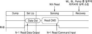
도 6을 참조하면, 도 6에서는 메모리 동작에 리커버리 구간이 포함되는 예가 도시된다. 독출 커맨드(CMD)가 메모리 장치로 수신되면, 메모리 장치는 상기 독출 커맨드(CMD)에 응답하여 셋업 구간(Set Up), 센싱 구간(Sensing), 리커버리 구간(Recovery) 및 덤프 구간(Dump)을 일련하게 수행할 수 있다. 변형 가능한 예로서, 메모리 동작에서 리커버리 구간(Recovery)와 덤프 구간(Dump)은 서로 순서가 변경되어도 무방하다. Referring to FIG. 6 , an example in which a recovery period is included in a memory operation is illustrated. When the read command CMD is received by the memory device, the memory device sequentially performs a setup section, a sensing section, a recovery section, and a dump section, in response to the read command CMD. can be performed As a deformable example, the order of the recovery section (Recovery) and the dump section (Dump) may be changed in the memory operation.
한편, 도 7은 본 발명의 실시예들에 따라 메모리 동작에서 리커버리 구간이 선택적으로 제거되는 예가 된다. 예컨대, 제2 독출 커맨드(CMD2) 및/또는 이에 수반되는 어드레스를 이용한 각종 판단 동작이 수행되고, 판단 결과에 따라 제1 독출 커맨드(CMD1)에 대한 제1 메모리 동작에서 리커버리 구간이 선택적으로 제거될 수 있다. 일 예로서, 리커버리 구간이 제거되지 않음에 따라, 제1 메모리 동작에서 셋업 구간(Set Up), 센싱 구간(Sensing), 리커버리 구간(Recovery) 및 덤프 구간(Dump)이 일련하게 수행될 수 있다. 반면에, 제3 독출 커맨드(CMD3) 및/또는 이에 수반되는 어드레스를 이용한 각종 판단 동작에 따라, 제2 독출 커맨드(CMD2)에 대한 제2 메모리 동작에서 리커버리 구간이 제거될 수 있다. 일 예로서, 리커버리 구간이 제거됨에 따라, 제2 메모리 동작에서 셋업 구간(Set Up), 센싱 구간(Sensing) 및 덤프 구간(Dump)이 일련하게 수행되고, 리커버리 동작은 수행되지 않는다.Meanwhile, FIG. 7 is an example in which a recovery period is selectively removed in a memory operation according to embodiments of the present invention. For example, various determination operations are performed using the second read command CMD2 and/or an address accompanying it, and the recovery period may be selectively removed in the first memory operation for the first read command CMD1 according to the determination result. can As an example, as the recovery section is not removed, a setup section (Set Up), a sensing section (Sensing), a recovery section (Recovery), and a dump section (Dump) may be sequentially performed in the first memory operation. On the other hand, the recovery period may be removed in the second memory operation for the second read command CMD2 according to various determination operations using the third read command CMD3 and/or an address accompanying the third read command CMD3 . As an example, as the recovery period is removed, in the second memory operation, a setup period (Set Up), a sensing period (Sensing), and a dump period (Dump) are sequentially performed, and the recovery operation is not performed.
도 8 및 도 9는 본 발명의 실시예들에 따른 메모리 장치의 동작방법을 나타내는 플로우차트이다. 8 and 9 are flowcharts illustrating a method of operating a memory device according to embodiments of the present invention.
도 8을 참조하면, 기록 및 독출 동작 등을 위해 다수의 커맨드들이 연속하게 메모리 장치로 제공될 수 있다. 메모리 장치는 제1 커맨드를 및 제1 어드레스를 수신하고(S11), 상기 제1 커맨드에 따른 제1 메모리 동작을 수행한다(S12). 전술한 실시예에서와 같이, 제1 메모리 동작은 기록 및 독출 등을 위한 다수의 구간들을 포함할 수 있다. Referring to FIG. 8 , a plurality of commands may be sequentially provided to the memory device for write and read operations. The memory device receives the first command and the first address (S11), and performs a first memory operation according to the first command (S12). As in the above-described embodiment, the first memory operation may include a plurality of sections for writing and reading.
이후, 제2 커맨드 및 이에 수반되는 제2 어드레스를 수신하고(S13), 상기 제2 커맨드 및 제2 어드레스 중 적어도 하나를 이용한 판단 동작을 수행한다(S14). 전술한 실시예에 따라 하나 이상의 다양한 판단 동작들이 수행될 수 있으며, 판단 결과에 따라 상기 제1 메모리 동작에서 리커버리 동작이 선택적으로 수행될 수 있다(S15). 만약, 상기 판단 결과에 따라 리커버리 동작이 스킵되는 경우, 리커버리 동작을 수행함이 없이 상기 제1 메모리 동작이 완료될 수 있으며, 이후 제2 커맨드에 따른 제2 메모리 동작이 수행될 수 있다(S16).Thereafter, the second command and the accompanying second address are received (S13), and a determination operation using at least one of the second command and the second address is performed (S14). According to the above-described embodiment, one or more various determination operations may be performed, and a recovery operation may be selectively performed in the first memory operation according to the determination result (S15). If the recovery operation is skipped according to the determination result, the first memory operation may be completed without performing the recovery operation, and then the second memory operation may be performed according to the second command ( S16 ).
도 9는 독출 동작에서 본 발명의 실시예에 따라 리커버리 구간이 스킵되는 예를 도시한다. 도 9를 참조하면, 메모리 장치는 제1 독출 커맨드를 수신하고(S21), 제1 독출 커맨드에 대응하여 제1 센싱 동작을 수행할 수 있다(S22). 또한, 메모리 장치는 제1 독출 커맨드에 이어 연속하게 제공되는 제2 커맨드를 수신할 수 있다(S22).9 illustrates an example in which a recovery section is skipped in a read operation according to an embodiment of the present invention. Referring to FIG. 9 , the memory device may receive a first read command ( S21 ) and perform a first sensing operation in response to the first read command ( S22 ). Also, the memory device may receive a second command continuously provided following the first read command ( S22 ).
리커버리 동작의 수행 여부를 판단하기 위하여, 제2 커맨드가 독출 동작을 요청하는 제2 독출 커맨드에 해당하는지를 판단한다(S24). 판단 결과, 제2 커맨드가 제2 독출 커맨드에 해당하지 않는 경우에는 제1 독출 커맨드에 대응하는 제1 메모리 동작에서 리커버리 동작이 수행될 수 있다(S25).In order to determine whether the recovery operation is performed, it is determined whether a second command corresponds to a second read command for requesting a read operation ( S24 ). As a result of the determination, when the second command does not correspond to the second read command, a recovery operation may be performed in the first memory operation corresponding to the first read command ( S25 ).
반면에, 제2 커맨드가 제2 독출 커맨드에 해당하는 경우에는, 상기 제2 커맨드의 수신 타이밍이 임계값 이전인지가 판단된다(S26). 상기 임계값은 다양하게 설정될 수 있으며, 예컨대 상기 임계값은 현재 독출 커맨드(예컨대, 제1 독출 커맨드)에 대응하여 수행되고 있는 제1 메모리 동작의 제1 센싱 구간의 완료 시점에 해당할 수 있다. 제2 커맨드가 상기 임계값 이후에 수신된 경우에는 제1 독출 커맨드에 대응하는 제1 메모리 동작에서 리커버리 동작이 수행될 수 있다(S25). 반면에, 제2 커맨드가 상기 임계값 이전에 수신된 경우에는 제1 독출 커맨드에 대응하는 제1 메모리 동작에서 리커버리 동작이 스킵될 수 있다(S27). 즉, 리커버리 동작을 수행함이 없이 상기 제1 독출 커맨드에 대한 제1 메모리 동작이 완료되고, 이후 제2 독출 커맨드에 대응하는 제2 센싱 동작이 수행될 수 있다(S28).On the other hand, when the second command corresponds to the second read command, it is determined whether the reception timing of the second command is before a threshold value (S26). The threshold value may be set in various ways. For example, the threshold value may correspond to the completion time of the first sensing period of the first memory operation being performed in response to the current read command (eg, the first read command). . When the second command is received after the threshold value, a recovery operation may be performed in a first memory operation corresponding to the first read command ( S25 ). On the other hand, when the second command is received before the threshold value, the recovery operation may be skipped in the first memory operation corresponding to the first read command ( S27 ). That is, the first memory operation for the first read command may be completed without performing a recovery operation, and thereafter, a second sensing operation corresponding to the second read command may be performed ( S28 ).
도 10은 본 발명의 실시예들에 따라 리커버리 동작의 다양한 스킵 예를 나타내는 표이다. 리커버리 구간에서 메모리 장치 내의 각종 라인들(예컨대, 워드 라인 및 비트 라인)로 인가된 전류 또는 전압 바이어스가 초기화(또는, 방전)될 수 있으며, 또는 바이어스 전압을 발생하는 각종 전압 발생기들의 출력(예컨대, 펌프 출력)을 초기화하는 예가 도시된다. 10 is a table illustrating various skip examples of a recovery operation according to embodiments of the present invention. In the recovery period, current or voltage bias applied to various lines (eg, word line and bit line) in the memory device may be initialized (or discharged), or outputs of various voltage generators generating bias voltage (eg, An example of initializing the pump output) is shown.
본 발명의 실시예들에 따라, 전술한 바와 같은 각종 판단 결과에 기반하여 리커버리 구간이 제거될 수 있다. 예컨대, 커맨드의 종류 및 수신 타이밍을 판단하여 리커버리 동작의 필요성 여부가 판단될 수 있으며, 리커버리 동작이 불필요한 것으로 판단되면 리커버리 구간이 제거될 수 있다.According to embodiments of the present invention, the recovery period may be removed based on various determination results as described above. For example, whether a recovery operation is necessary may be determined by determining the type and reception timing of the command, and if it is determined that the recovery operation is unnecessary, the recovery period may be removed.
리커버리 구간이 제거되는 경우, 독출 동작을 위한 센싱 동작의 종료 후에도 워드 라인(WL)에 인가된 바이어스 및 비트 라인(BL)에 인가된 바이어스가 방전되지 않고 현재 상태가 유지된다. 또한, 독출 동작을 위한 바이어스를 제공하는 펌프(Pump)의 출력 또한 초기화되지 않고 현재 상태가 유지된다. When the recovery period is removed, the bias applied to the word line WL and the bias applied to the bit line BL are not discharged and the current state is maintained even after the sensing operation for the read operation is terminated. In addition, the output of the pump that provides the bias for the read operation is also not initialized and the current state is maintained.
한편, 일 실시예에 따라, 리커버리 동작이 불필요한 것으로 판단되더라도 리커버리 구간은 유지되고 일부의 구성들에 대해서만 리커버리 동작이 스킵될 수 있다. 예컨대, 리커버리 구간에서, 비트 라인(BL)과 펌프(Pump)에 대해서만 리커버리 동작이 스킵되는 반면에, 워드 라인(WL)에 대해서는 리커버리 동작이 수행됨에 따라 워드 라인(WL)에 인가된 전압 바이어스가 방전될 수 있다. Meanwhile, according to an embodiment, even if it is determined that the recovery operation is unnecessary, the recovery period may be maintained and the recovery operation may be skipped only for some components. For example, in the recovery period, while the recovery operation is skipped only for the bit line BL and the pump, the voltage bias applied to the word line WL is applied as the recovery operation is performed for the word line WL. can be discharged.
다른 예로서, 리커버리 구간에서, 펌프(Pump)의 일부 및 비트 라인(BL)에 대해서만 리커버리 동작이 스킵되는 반면에, 워드 라인(WL)에 대해서는 리커버리 동작이 수행됨에 따라 워드 라인(WL)에 인가된 전압 바이어스가 방전될 수 있다. 또한, 워드 라인(WL)으로 바이어스를 제공하는 일부의 펌프(Pump)의 출력이 초기화될 수 있다. As another example, in the recovery period, while the recovery operation is skipped only for a part of the pump and the bit line BL, the recovery operation is performed for the word line WL, and thus the word line WL is applied. The applied voltage bias may be discharged. Also, outputs of some pumps that provide a bias to the word line WL may be initialized.
또한 다른 예로서, 리커버리 구간에서, 워드 라인(WL)과 펌프(Pump)에 대해서만 리커버리 동작이 스킵되는 반면에, 비트 라인(BL)에 대해서는 리커버리 동작이 수행됨에 따라 워드 라인(WL)에 인가된 전압 바이어스가 방전될 수 있다.Also, as another example, in the recovery period, the recovery operation is skipped only for the word line WL and the pump, while the recovery operation is performed for the bit line BL. A voltage bias may be discharged.
또한 다른 예로서, 리커버리 구간에서, 펌프(Pump)의 일부 및 워드 라인(WL)에 대해서만 리커버리 동작이 스킵되는 반면에, 비트 라인(BL)에 대해서는 리커버리 동작이 수행됨에 따라 비트 라인(BL)에 인가된 전압 바이어스가 방전될 수 있다. 또한, 비트 라인(BL)으로 바이어스를 제공하는 일부의 펌프(Pump)의 출력이 초기화될 수 있다.Also, as another example, in the recovery period, the recovery operation is skipped only for a part of the pump and the word line WL, while the recovery operation is performed for the bit line BL. The applied voltage bias may be discharged. Also, outputs of some pumps that provide a bias to the bit line BL may be initialized.
도 10에 도시된 리커버리 동작은 본 발명의 실시예들에 적용될 수 있는 하나의 예에 불과한 것으로서, 본 발명의 실시예들은 다양하게 변경이 가능하다. 예컨대, 리커버리 구간에서 다른 다양한 구성들에 대해 초기화 동작이 수행될 수 있으며, 본 발명의 실시예들에 따른 판단 결과에 따라 리커버리 구간이 제거되거나, 또는 다양한 구성들이 선택적으로 리커버리 동작이 스킵될 수 있다. The recovery operation shown in FIG. 10 is only one example that can be applied to the embodiments of the present invention, and various modifications are possible in the embodiments of the present invention. For example, an initialization operation may be performed for various other configurations in the recovery period, the recovery period may be removed according to a determination result according to embodiments of the present invention, or the recovery operation may be selectively skipped in various configurations. .
도 11 및 도 12는 본 발명의 실시예들에 따른 메모리 장치의 각종 동작 구간을 나타내는 타이밍도이다. 11 and 12 are timing diagrams illustrating various operation sections of a memory device according to embodiments of the present invention.
도 11을 참조하면, 제1 독출 커맨드(CMD_RD1)가 수신됨에 따라 제1 메모리 동작이 수행되고, 예컨대 상기 제1 메모리 동작에서 셋업 동작(Set Up), 센싱 동작(또는, 독출 동작(Read Operation)), 리커버리 동작(Recovery) 및 덤프 동작(Dump)이 일련하게 수행된다. 제1 독출 커맨드(CMD_RD1)가 수신됨에 따라 레디/비지 신호(RnB)가 로우 레벨(L)로 천이되고, 독출 동작(Read Operation)이 완료됨에 따라 레디/비지 신호(RnB)가 하이 레벨(H)로 천이된다. 레디/비지 신호(RnB)가 하이 레벨(H)인 동안에 제2 독출 커맨드(CMD_RD2)가 수신될 수 있다. 또한, 제2 독출 커맨드(CMD_RD2)가 수신됨에 따라 레디/비지 신호(RnB)가 로우 레벨(L)로 천이될 수 있으며, 덤프 동작(Dump)이 완료됨에 따라 레디/비지 신호(RnB)는 다시 하이 레벨(H)로 천이될 수 있다. 상기 제2 독출 커맨드(CMD_RD2)가 제1 독출 커맨드(CMD_RD1)에 따른 독출 동작(Read Operation)이 종료된 이후에 수신되었으므로(또는, 리커버리 동작이 수행되는 도중에 수신되었으므로), 제1 메모리 동작에서 리커버리 동작(Recovery)은 스킵되지 않는다. Referring to FIG. 11 , as the first read command CMD_RD1 is received, a first memory operation is performed, for example, a setup operation (Set Up) and a sensing operation (or a read operation) in the first memory operation. ), a recovery operation (Recovery), and a dump operation (Dump) are sequentially performed. As the first read command CMD_RD1 is received, the ready/busy signal RnB transitions to the low level L, and as the read operation is completed, the ready/busy signal RnB changes to the high level H ) is transitioned to The second read command CMD_RD2 may be received while the ready/busy signal RnB is at the high level H. Also, as the second read command CMD_RD2 is received, the ready/busy signal RnB may transition to the low level L, and as the dump operation Dump is completed, the ready/busy signal RnB is again It may transition to a high level (H). Since the second read command CMD_RD2 is received after a read operation according to the first read command CMD_RD1 is finished (or received while the recovery operation is being performed), recovery is performed in the first memory operation The operation (Recovery) is not skipped.
상기 제2 독출 커맨드(CMD_RD2)에 대응하여 제2 메모리 동작이 수행될 수 있다. 제1 독출 커맨드(CMD_RD1)에 따라 독출된 데이터(Data)는 덤프 동작(Dump)을 통해 페이지 버퍼에서 입출력 버퍼로 이동되었으므로, 제2 메모리 동작이 수행되는 도중에 입출력 버퍼에 저장된 데이터(Data)는 메모리 콘트롤러로 제공될 수 있다. 예컨대, 데이터 요청 신호(/RE)가 활성화됨에 따라 데이터(Data)가 메모리 장치에서 메모리 콘트롤러로 제공될 수 있다(Data Out).A second memory operation may be performed in response to the second read command CMD_RD2 . Since the data read according to the first read command CMD_RD1 is moved from the page buffer to the input/output buffer through the dump operation, the data stored in the input/output buffer during the second memory operation is stored in the memory. It may be provided as a controller. For example, as the data request signal /RE is activated, data Data may be provided from the memory device to the memory controller (Data Out).
이와 유사하게, 제2 독출 커맨드(CMD_RD2)에 대응하여 제2 메모리 동작이 수행되는 도중에 제3 독출 커맨드(CMD_RD3)가 수신될 수 있다. 상기 제3 독출 커맨드(CMD_RD3)가 수신될 때, 상기 제3 독출 커맨드(CMD_RD3)의 종류를 판단하는 동작, 제3 독출 커맨드(CMD_RD3)의 수신 타이밍을 판단하는 동작, 제3 독출 커맨드(CMD_RD3)에 수반되는 어드레스를 판단하는 동작 등이 수행될 수 있다. 상기 제3 독출 커맨드(CMD_RD3)가 제2 독출 커맨드(CMD_RD2)에 따른 독출 동작(Read Operation)이 종료되기 전에 수신되었으므로(또는, 리커버리 동작이 수행되기 전에 수신되었으므로), 제2 메모리 동작에서 리커버리 동작(Recovery)은 스킵될 수 있다(또는, 리커버리 구간은 제거(deleted)될 수 있다).Similarly, the third read command CMD_RD3 may be received while the second memory operation is performed in response to the second read command CMD_RD2 . When the third read command CMD_RD3 is received, the operation of determining the type of the third read command CMD_RD3 , the operation of determining the reception timing of the third read command CMD_RD3 , and the third read command CMD_RD3 An operation of determining an address accompanying the . Since the third read command CMD_RD3 is received before a read operation according to the second read command CMD_RD2 is completed (or is received before the recovery operation is performed), a recovery operation in the second memory operation is performed. (Recovery) may be skipped (or the recovery period may be deleted).
이와 유사하게, 제3 독출 커맨드(CMD_RD3)에 대응하여 제3 메모리 동작이 수행되는 도중에 제4 독출 커맨드(CMD_RD4)가 수신되고, 각종 판단 결과에 따라 제3 메모리 동작에서 리커버리 동작(Recovery)은 스킵될 수 있다. 한편, 제4 독출 커맨드(CMD_RD4)가 연속되는 독출 동작에서의 마지막 커맨드인 것으로 가정할 때, 제4 독출 커맨드(CMD_RD4)에 따른 제4 메모리 동작이 수행되는 도중에 해당 독출 동작이 마지막 독출 동작임을 나타내는 커맨드(Last CMD)가 수신될 수 있다. 일 실시예에 따라, 상기 커맨드(Last CMD)가 수신되는 경우, 제4 메모리 동작에서 리커버리 동작(Recovery)은 스킵되지 않을 수 있다.Similarly, the fourth read command CMD_RD4 is received while the third memory operation is being performed in response to the third read command CMD_RD3, and the recovery operation is skipped in the third memory operation according to various determination results. can be Meanwhile, assuming that the fourth read command CMD_RD4 is the last command in successive read operations, indicating that the corresponding read operation is the last read operation while the fourth memory operation according to the fourth read command CMD_RD4 is being performed A command (Last CMD) may be received. According to an embodiment, when the command Last CMD is received, the recovery operation in the fourth memory operation may not be skipped.
도 11에 도시된 본 발명의 동작은 하나의 실시예에 불과한 것으로서, 일 실시예에 따라 리커버리 동작(Recovery)과 덤프 동작(Dump)의 순서는 변경되어도 무방하다. 이 때, 리커버리 동작(Recovery)의 수행 여부를 판단하는 기준도 함께 변경되어도 무방하다. 예컨대, 제2 및 제3 독출 커맨드(CMD_RD2, CMD_RD3)를 참조하면, 제2 독출 커맨드(CMD_RD2)의 리커버리 동작(Recovery)이 수행되기 이전에 제3 독출 커맨드(CMD_RD3)가 수신되는 경우에는 제2 메모리 동작에서 리커버리 동작(Recovery)은 스킵될 수 있다. 이 때, 제3 독출 커맨드(CMD_RD3)는 제2 독출 커맨드(CMD_RD3)에 따른 독출 동작(Read Operation)이 종료된 이후에 수신되더라도, 덤프 동작(Dump)이 종료되기 전에 수신된 경우에는 상기 리커버리 동작(Recovery)은 스킵될 수 있다.The operation of the present invention shown in FIG. 11 is only one embodiment, and the order of the recovery operation (Recovery) and the dump operation (Dump) may be changed according to an embodiment. In this case, the criterion for determining whether to perform the recovery operation may also be changed. For example, referring to the second and third read commands CMD_RD2 and CMD_RD3 , when the third read command CMD_RD3 is received before the recovery operation of the second read command CMD_RD2 is performed, the second read command CMD_RD3 is received. In the memory operation, the recovery operation may be skipped. In this case, even if the third read command CMD_RD3 is received after the read operation according to the second read command CMD_RD3 is finished, if the third read command CMD_RD3 is received before the dump operation ends, the recovery operation is performed. (Recovery) can be skipped.
한편, 도 12는 메모리 동작에서 전체 리커버리 구간을 제거함이 없이 리커버리 동작을 스킵하는 예를 나타낸다. 도 12에 도시된 바와 같이, N 번째 독출 커맨드에 따른 독출 동작(Nth Read)이 수행되는 도중에 다음의 독출 커맨드(예컨대, N+1번째 독출 커맨드)가 수신됨에 따라, N 번째 메모리 동작에서 리커버리 동작(Recovery)이 스킵될 수 있다. 이 때, 리커버리 구간이 제거됨이 없이, 일부의 구성 요소들에 대해서만 리커버리 동작(Recovery)이 스킵될 수 있다.Meanwhile, FIG. 12 shows an example of skipping the recovery operation without removing the entire recovery period in the memory operation. 12 , as a next read command (eg, an N+1th read command) is received while a read operation (Nth Read) according to an Nth read command is performed, a recovery operation in an Nth memory operation (Recovery) can be skipped. In this case, the recovery operation may be skipped only for some components without removing the recovery period.
만약, 리커버리 동작(Recovery)이 워드 라인, 비트 라인 및 펌프에 대한 초기화 동작을 포함하는 경우, 상기 리커버리 구간에서 일부의 구성들에 대해서만 선택적으로 리커버리 동작이 스킵될 수 있다. 일 예로서, N 번째 메모리 동작에서 워드 라인에 대한 전압 바이어스 방전 동작이 스킵되는 반면에, 비트 라인 및 펌프 등 나머지 구성 요소들의 리커버리 동작은 수행될 수 있다. 리커버리 동작이 스킵되는 구성 요소들은 다양한 방식으로 선택이 가능하다. If the recovery operation includes an initialization operation for the word line, the bit line, and the pump, the recovery operation may be selectively skipped only for some components in the recovery period. As an example, in the Nth memory operation, the voltage bias discharge operation for the word line may be skipped, while the recovery operation of the remaining components such as the bit line and the pump may be performed. Components for which the recovery operation is skipped can be selected in various ways.
도 13은 본 발명의 실시예들에 따른 메모리 장치의 동작 예를 나타내는 파형도이다. 예컨대, 도 13에서는 메모리 장치에 대한 독출 동작에서 리커버리 구간이 제거되는 경우와 그렇지 않은 경우에서의 각종 전압 레벨의 파형도가 도시된다. 13 is a waveform diagram illustrating an operation example of a memory device according to embodiments of the present invention. For example, FIG. 13 shows waveforms of various voltage levels in a case in which a recovery period is removed and in a case in which a recovery period is not removed in a read operation of the memory device.
어느 하나의 독출 커맨드에 대한 메모리 동작에서, 셋업 구간(t0 ~ t1)이 수행됨에 따라 스트링 선택 라인(SSL), 비선택 워드 라인(Unsel WL), 비트 라인(BL) 등의 전압 레벨이 상승될 수 있다. 도 13의 예에서는 선택 워드 라인(Sel WL)의 전압 레벨(Vrd)이 비선택 워드 라인(Unsel WL)의 전압 레벨(Vread) 보다 낮음에 따라, 선택 워드 라인(Sel WL)의 전압 레벨(Vrd)이 센싱 구간(t1 ~ t2)에서 상승되는 것으로 도시되었으나 본 발명의 실시예는 이에 국한될 필요는 없다. 예컨대, 선택 워드 라인(Sel WL)의 전압 레벨(Vrd)은 셋업 구간(Set Up)에서 상승되어도 무방하다. In the memory operation for any one read command, as the setup period t0 to t1 is performed, the voltage level of the string selection line SSL, the unselected word line Unsel WL, and the bit line BL may increase. can In the example of FIG. 13 , as the voltage level Vrd of the selected word line Sel WL is lower than the voltage level Vread of the unselected word line Unsel WL, the voltage level Vrd of the selected word line Sel WL is ) is shown to increase in the sensing period t1 to t2, but the embodiment of the present invention is not limited thereto. For example, the voltage level Vrd of the selected word line Sel WL may be increased in the setup period Set Up.
센싱 구간(t1 ~ t2)에서 메모리 셀에 저장된 데이터에 따라, 비트 라인(BL)의 전압 레벨은 프리차지 레벨에서 점차 상승하거나 또는 하강한다. 비트 라인(BL)의 전압 레벨이 디벨로프된 상태에서 데이터의 센싱이 수행되고, 센싱된 데이터는 메모리 장치 내의 페이지 버퍼에 저장될 수 있다. 이후, 리커버리 구간(t2 ~ t3)에서 리커버리 동작이 수행되는 경우의 신호의 파형은 점선으로 도시된 바와 같이 변동된다. 반면에, 리커버리 구간(t2 ~ t3)이 제거되는 경우에는, 도 13에 도시된 파형도에서 상기 센싱 구간(t1 ~ t2) 이후에 리커버리가 수행됨이 없이 덤프 구간(t3 ~ t4)으로 바로 진입될 수 있다.In the sensing period t1 to t2, the voltage level of the bit line BL gradually increases or decreases from the precharge level according to data stored in the memory cell. Sensing of data may be performed while the voltage level of the bit line BL is developed, and the sensed data may be stored in a page buffer in the memory device. Thereafter, the waveform of the signal when the recovery operation is performed in the recovery period t2 to t3 is changed as shown by the dotted line. On the other hand, when the recovery section (t2 ~ t3) is removed, the dump section (t3 ~ t4) without recovery is performed after the sensing interval (t1 ~ t2) in the waveform diagram shown in FIG. can
예컨대, 리커버리 구간(t2 ~ t3)이 제거되는 경우에는 스트링 선택 라인(SSL), 선택 워드 라인(Sel WL) 및 비선택 워드 라인(Unsel WL)들의 전압 레벨이 이전 구간의 상태를 유지할 수 있는 반면에, 리커버리 구간(t2 ~ t3)에서 리커버리 동작이 수행되는 경우에는 스트링 선택 라인(SSL), 선택 워드 라인(Sel WL) 및 비선택 워드 라인(Unsel WL)들의 전압 레벨이 접지전압 레벨 등의 초기화 상태로 변동될 수 있다. 이후, 덤프 구간(t3 ~ t4)이 수행됨에 따라 페이지 버퍼에 저장된 데이터는 입출력 버퍼로 전달되고, 다음의 독출 커맨드에 대응하여 셋업 구간 내지 덤프 구간이 일련하게 수행될 수 있다. For example, when the recovery period t2 to t3 is removed, the voltage levels of the string selection line SSL, the selected word line Sel WL, and the unselected word line Unsel WL may maintain the state of the previous period. For example, when the recovery operation is performed in the recovery period t2 to t3, the voltage levels of the string selection line SSL, the selected word line Sel WL, and the unselected word line Unsel WL are initialized to the ground voltage level. state can be changed. Thereafter, as the dump sections t3 to t4 are performed, the data stored in the page buffer is transferred to the input/output buffer, and the setup section or the dump section can be sequentially performed in response to the next read command.
다른 예로서, 전술한 실시예에서와 동일 또는 유사하게, 각종 판단 결과에 따라 리커버리 동작이 스킵되는 것으로 선택되더라도, 상기 리커버리 구간(t2 ~ t3)이 메모리 동작에 포함될 수 있다. 이 때, 상기 리커버리 구간(t2 ~ t3)에서 일부의 구성 요소들의 리커버리 동작은 스킵되는 반면에, 다른 일부의 구성 요소들에 대해서는 리커버리 동작이 수행될 수 있다.As another example, the recovery period t2 to t3 may be included in the memory operation even if the recovery operation is selected to be skipped according to various determination results, identically or similarly to the above-described embodiment. In this case, in the recovery period t2 to t3, the recovery operation of some of the components may be skipped, while the recovery operation may be performed on some of the other components.
도 14는 본 발명의 일 실시예에 따른 메모리 장치에 포함되는 제어 로직의 구현 예를 나타내는 블록도이다. 도 14에 도시된 구성요소들의 동작을 설명함에 있어서, 전술한 실시예에서와 동일한 구성요소들은 그 동작 또한 동일 또는 유사하므로 이에 대한 구체적인 설명은 생략된다.14 is a block diagram illustrating an implementation example of control logic included in a memory device according to an embodiment of the present invention. In describing the operation of the components shown in FIG. 14 , the same components as in the above-described embodiment also have the same or similar operations, and thus a detailed description thereof will be omitted.
도 14에 도시된 바와 같이, 제어 로직(200)은 커맨드 판단부(210), 타이밍 판단부(220), 어드레스 비교부(230) 및 리커버리 수행부(240)를 포함할 수 있다. 제어 로직(200)은 메모리 콘트롤러로부터 수신되는 커맨드 및/또는 어드레스에 기반하여 메모리 동작에서 리커버리 구간을 제거할 지 여부를 판단하고, 그 판단 결과에 따라 리커버리 동작을 제어할 수 있다. 14 , the
커맨드 판단부(210)는 디코딩된 커맨드(CMD_dec)를 판단함으로써 메모리 콘트롤러로부터의 커맨드가 독출 커맨드인지를 판단하고, 타이밍 판단부(220)는 메모리 콘트롤러로부터의 커맨드가 현재 메모리 동작의 센싱 구간이 종료되기 전에 수신되었는지를 판단한다. 일 예로서, 제1 및 제2 독출 커맨드들이 연속하게 수신되고, 제2 독출 커맨드가 제1 메모리 동작의 센싱 구간이 종료되기 전에 수신된 경우에는 리커버리 구간을 제거하기 위한 판단 결과가 어드레스 비교부(230)로 제공될 수 있다. The
어드레스 비교부(230)는 제1 독출 커맨드에 수반되는 제1 어드레스(ADD1)와 제2 독출 커맨드에 수반되는 제2 어드레스(ADD2)를 비교할 수 있다. 일 예로서, 어드레스 비교부(230)는 제1 어드레스(ADD1)와 제2 어드레스(ADD2)의 동일성 여부를 비교할 수 있다. 또한, 제1 어드레스(ADD1)는 제1 로우 어드레스와 제1 칼럼 어드레스를 포함할 수 있으며, 제2 어드레스(ADD2)는 제2 로우 어드레스와 제2 칼럼 어드레스를 포함할 수 있다. 일 예로서, 어드레스 비교부(230)는 제1 로우 어드레스와 제2 로우 어드레스의 동일성 여부를 비교할 수 있으며, 또한 어드레스 비교부(230)는 제1 칼럼 어드레스와 제2 칼럼 어드레스의 동일성 여부를 비교할 수 있다.The
본 발명의 실시예에 따르면, 상기 어드레스 비교 결과에 따라 다양한 방식으로써 리커버리 구간이 제거되거나 리커버리 동작이 수행될 수 있다. 예컨대, 전술한 조건(예컨대, 제2 독출 커맨드가 제1 메모리 동작의 센싱 구간의 종료 이전에 수신된 경우)을 만족하는 상태에서, 제1 어드레스(ADD1)와 제2 어드레스(ADD2)의 비교 결과에 따라 리커버리 구간이 제거되거나 리커버리 동작이 수행될 수 있다. According to an embodiment of the present invention, a recovery section may be removed or a recovery operation may be performed in various ways according to the address comparison result. For example, a comparison result of the first address ADD1 and the second address ADD2 in a state where the above-described condition (eg, the second read command is received before the end of the sensing period of the first memory operation) is satisfied Accordingly, the recovery section may be removed or a recovery operation may be performed.
일 동작 예로서, 제1 메모리 동작에서 선택된 워드 라인(또는, 페이지)와 제2 메모리 동작에서 선택된 워드 라인(또는, 페이지)이 동일한 경우에, 제1 메모리 동작에서 리커버리 구간이 제거될 수 있다. 예컨대, 제1 및 제2 메모리 동작들에서 동일한 워드 라인이 선택되는 경우에는, 제1 메모리 동작에서의 스트링 선택 라인(SSL), 선택 워드 라인(Sel WL) 및 비선택 워드 라인(Unsel WL)의 전압 바이어스와 제2 메모리 동작에서의 전압 바이어스가 서로 동일하다. 전술한 도 13의 파형도를 참조하면, 제1 메모리 동작의 센싱 구간(t1 ~ t2) 이후의 스트링 선택 라인(SSL), 선택 워드 라인(Sel WL) 및 비선택 워드 라인(Unsel WL)의 전압 레벨이 제2 메모리 동작의 셋업 구간(t4 ~ t5)이 종료될 때의 전압 레벨과 유사한 값을 가지며, 이에 따라 제1 메모리 동작에서 리커버리 구간이 제거될 수 있다. As an example of an operation, when the word line (or page) selected in the first memory operation is the same as the word line (or page) selected in the second memory operation, the recovery period may be removed in the first memory operation. For example, when the same word line is selected in the first and second memory operations, the string select line SSL, the selected word line Sel WL, and the unselected word line Unsel WL are selected in the first memory operation. The voltage bias and the voltage bias in the second memory operation are the same. Referring to the waveform diagram of FIG. 13 described above, voltages of the string selection line SSL, the selected word line Sel WL, and the unselected word line Unsel WL after the sensing period t1 to t2 of the first memory operation The level has a value similar to the voltage level when the setup period t4 to t5 of the second memory operation ends, and accordingly, the recovery period may be removed from the first memory operation.
반면에, 제1 로우 어드레스와 제2 로우 어드레스가 서로 다른 경우에는, 제1 및 제2 메모리 동작에서 선택 워드 라인(Sel WL) 및 비선택 워드 라인(Unsel WL)의 전압 바이어스가 변동될 수 있으며, 이에 따라 제1 메모리 동작에서 센싱 구간(t1 ~ t2)이 종료된 후 리커버리 동작이 수행될 수 있다. On the other hand, when the first row address and the second row address are different from each other, the voltage bias of the selected word line Sel WL and the unselected word line Unsel WL may be changed in the first and second memory operations, Accordingly, the recovery operation may be performed after the sensing period t1 to t2 in the first memory operation is terminated.
한편, 비트 라인과 관련하여, 제1 메모리 동작에서 선택된 비트 라인은 센싱 동작을 통해 그 전압 레벨이 디벨로프되고, 이에 따라 센싱 동작이 수행된 비트 라인의 전압은 프리차지 레벨에서 로직 하이(또는, 로직 로우) 레벨로 변동될 수 있다. 본 발명의 일 실시예에 따라, 제1 칼럼 어드레스에 대응하여 선택된 비트 라인들과 제2 칼럼 어드레스에 대응하여 선택된 비트 라인들의 동일한지 여부에 따라 리커버리 구간이 제거되거나 리커버리 동작이 수행될 수 있다. 예컨대, 제1 칼럼 어드레스와 제2 칼럼 어드레스가 서로 상이한 경우에 리커버리 구간이 제거될 수 있다. Meanwhile, with respect to the bit line, the voltage level of the bit line selected in the first memory operation is developed through the sensing operation, and accordingly, the voltage of the bit line on which the sensing operation is performed is set at a logic high (or, logic low) level. According to an embodiment of the present invention, a recovery period may be removed or a recovery operation may be performed depending on whether the bit lines selected corresponding to the first column address and the bit lines selected corresponding to the second column address are the same. For example, when the first column address and the second column address are different from each other, the recovery period may be removed.
전술한 실시예에 따른 메모리 장치의 동작 예를 도 15 및 도 16을 참조하여 설명한다. 도 15 및 도 16은 도 14의 메모리 장치의 리커버리 동작의 일 예를 나타내는 블록도이다. An operation example of the memory device according to the above-described embodiment will be described with reference to FIGS. 15 and 16 . 15 and 16 are block diagrams illustrating an example of a recovery operation of the memory device of FIG. 14 .
도 15를 참조하면, 메모리 셀 어레이에서 어느 하나의 블록(BLK)은 다수 개의 페이지들을 포함하며, 각각의 페이지는 로우 어드레스에 의해 지시될 수 있다. 제1 독출 커맨드(CMD_RD1) 내지 제5 독출 커맨드(CMD_RD5)가 연속하게 메모리 장치로 제공되는 것으로 가정한다. 또한, 제1 독출 커맨드(CMD_RD1) 내지 제5 독출 커맨드(CMD_RD5) 각각의 수신 타이밍이 전술한 실시예들에서의 조건(센싱 구간이 완료되기 전에 독출 커맨드 수신)을 만족하는 것으로 가정한다.Referring to FIG. 15 , any one block BLK in the memory cell array includes a plurality of pages, and each page may be indicated by a row address. It is assumed that the first read command CMD_RD1 to the fifth read command CMD_RD5 are sequentially provided to the memory device. Also, it is assumed that the reception timing of each of the first read commands CMD_RD1 to CMD_RD5 satisfies the condition (reception of the read command before the sensing period is completed) in the above-described embodiments.
제1 독출 커맨드(CMD_RD1)의 로우 어드레스가 제1 값(ADD_R1)을 갖는 경우, 제1 독출 커맨드(CMD_RD1)에 따라 제1 페이지(PAGE 1)의 적어도 일부의 데이터가 독출될 수 있다. 이후의 제2 독출 커맨드(CMD_RD2)의 로우 어드레스가 제1 값(ADD_R1)을 가짐에 따라 제1 및 제2 독출 커맨드(CMD_RD1, CMD_RD2)에 수반되는 로우 어드레스가 서로 동일한 경우, 제1 독출 커맨드(CMD_RD1)에 대응하는 센싱 동작이 종료된 이후에 워드 라인에 대한 리커버리 동작은 스킵될 수 있다. When the row address of the first read command CMD_RD1 has the first value ADD_R1 , at least a portion of data of the
반면에, 이후의 제3 독출 커맨드(CMD_RD3)의 로우 어드레스가 제2 값(ADD_R2)을 가짐에 따라, 제2 및 제3 독출 커맨드(CMD_RD2, CMD_RD3)에 수반되는 로우 어드레스가 서로 상이할 수 있다. 이에 따라, 제2 독출 커맨드(CMD_RD2)에 대응하는 센싱 동작이 종료된 이후에, 워드 라인에 대한 리커버리 동작이 수행됨에 따라 상기 워드 라인이 초기화될 수 있다. On the other hand, as the row address of the subsequent third read command CMD_RD3 has the second value ADD_R2 , row addresses accompanying the second and third read commands CMD_RD2 and CMD_RD3 may be different from each other. . Accordingly, after the sensing operation corresponding to the second read command CMD_RD2 is terminated, the word line may be initialized as the recovery operation is performed on the word line.
한편, 전술한 방식와 동일하게 다음의 독출 커맨드들에 대한 동작이 수행될 수 있다. 예컨대, 제4 독출 커맨드(CMD_RD4)의 로우 어드레스가 제3 값(ADD_R3)을 가짐에 따라, 제3 및 제4 독출 커맨드(CMD_RD3, CMD_RD4)에 수반되는 로우 어드레스가 서로 상이할 수 있다. 이에 따라, 제3 독출 커맨드(CMD_RD3)에 대응하는 센싱 동작이 종료된 이후에 워드 라인에 대한 리커버리 동작이 수행될 수 있다. 반면에, 제5 독출 커맨드(CMD_RD5)의 로우 어드레스가 제3 값(ADD_R3)을 가짐에 따라, 제4 및 제5 독출 커맨드(CMD_RD4, CMD_RD5)에 수반되는 로우 어드레스가 서로 동일할 수 있다. 이에 따라, 제4 독출 커맨드(CMD_RD4)에 대응하는 센싱 동작이 종료된 이후에 워드 라인에 대한 리커버리 동작이 스킵될 수 있다.Meanwhile, operations for the following read commands may be performed in the same manner as described above. For example, as the row address of the fourth read command CMD_RD4 has the third value ADD_R3 , row addresses accompanying the third and fourth read commands CMD_RD3 and CMD_RD4 may be different from each other. Accordingly, after the sensing operation corresponding to the third read command CMD_RD3 is terminated, the recovery operation for the word line may be performed. On the other hand, as the row address of the fifth read command CMD_RD5 has the third value ADD_R3 , row addresses accompanying the fourth and fifth read commands CMD_RD4 and CMD_RD5 may be the same. Accordingly, after the sensing operation corresponding to the fourth read command CMD_RD4 is terminated, the recovery operation for the word line may be skipped.
상기 도 15의 실시예에서는 워드 라인에 대한 리커버리 동작의 스킵 또는 수행 여부가 설명되었으나, 전술한 실시예에서와 유사하게 비트 라인이나 펌프 출력에 대한 리커버리 동작이 함께 수행되어도 무방하다. 또한, 상기 어드레스 비교 결과에 따라 메모리 동작에서 리커버리 구간이 제거될 수 있으며, 또는 리커버리 구간은 포함되되 일부의 구성 요소들에 대한 리커버리 동작만이 스킵되어도 무방하다. In the embodiment of FIG. 15 , whether the recovery operation for the word line is skipped or performed has been described, but similarly to the above-described embodiment, the recovery operation for the bit line or the pump output may be performed together. In addition, the recovery period may be removed from the memory operation according to the address comparison result, or the recovery period may be included but only the recovery operation for some components may be skipped.
한편, 도 16을 참조하면, 칼럼 어드레스를 비교한 결과에 기반하여 리커버리 동작의 스킵 여부가 판단될 수 있다. 도 16에서는 그 일 예로서, 현재의 독출 커맨드의 칼럼 어드레스와 다음의 독출 커맨드의 칼럼 어드레스가 서로 상이할 때, 현재의 메모리 동작에서 리커버리 구간이 동작이 스킵되는 예가 설명된다.Meanwhile, referring to FIG. 16 , it may be determined whether the recovery operation is skipped based on a result of comparing column addresses. 16 illustrates an example in which a recovery section operation is skipped in a current memory operation when a column address of a current read command is different from a column address of a next read command.
각각의 페이지(PAGE)는 다수 개의 셀 영역들을 포함할 수 있으며, 예컨대 상기 페이지(PAGE)는 다수 개의 섹터들(SEC)을 포함할 수 있다. 상기와 같은 셀 영역들은 다양하게 정의가 가능하며, 예컨대 동일한 워드 라인에 연결되는 메모리 셀들이 하나의 페이지(PAGE)로 정의될 수 있다. 또한, 메모리 장치의 기록/독출 단위는 상기 페이지(PAGE)의 일부에 해당하는 사이즈를 가질 수 있으며, 상기 섹터(SEC)가 메모리 장치의 기록/독출 단위에 해당할 수 있다. 또는, 섹터(SEC)는 메모리 장치의 에러 정정 및 검출 단위에 해당할 수 있다. Each page PAGE may include a plurality of cell regions, for example, the page PAGE may include a plurality of sectors SEC. The above cell regions may be defined in various ways, for example, memory cells connected to the same word line may be defined as one page. Also, a write/read unit of the memory device may have a size corresponding to a portion of the page PAGE, and the sector SEC may correspond to a write/read unit of the memory device. Alternatively, the sector SEC may correspond to an error correction and detection unit of the memory device.
제1 독출 커맨드(CMD_RD1) 내지 제5 독출 커맨드(CMD_RD5)가 연속하게 메모리 장치로 제공되고, 각각의 독출 커맨드에 수반되는 어드레스의 일부는 메모리 셀들의 칼럼을 지시하기 위한 칼럼 어드레스일 수 있다. 일 예로서, 각각의 독출 커맨드에 수반되는 칼럼 어드레스에 따라 페이지(PAGE)의 어느 하나의 섹터(SEC)가 선택될 수 있다. The first read command CMD_RD1 to the fifth read command CMD_RD5 are successively provided to the memory device, and a portion of the address accompanying each read command may be a column address for indicating a column of memory cells. As an example, any one sector SEC of the page PAGE may be selected according to a column address accompanying each read command.
제1 독출 커맨드(CMD_RD1)의 칼럼 어드레스가 제1 섹터(SEC1)를 지시하는 제1 값(ADD_C1)을 가짐에 따라 제1 섹터(SEC1)의 데이터가 독출될 수 있다. 한편, 이후의 제2 독출 커맨드(CMD_RD2)의 칼럼 어드레스가 제1 섹터(SEC1)를 지시하는 제1 값(ADD_C1)을 가짐에 따라, 제1 독출 커맨드(CMD_RD1)와 제2 독출 커맨드(CMD_RD2)의 칼럼 어드레스가 서로 동일할 수 있다. 이에 따라, 제1 독출 커맨드(CMD_RD1)에 대응하는 센싱 동작이 종료된 이후에 비트 라인에 대한 리커버리 동작이 수행될 수 있다.As the column address of the first read command CMD_RD1 has a first value ADD_C1 indicating the first sector SEC1 , data of the first sector SEC1 may be read. Meanwhile, as the column address of the subsequent second read command CMD_RD2 has the first value ADD_C1 indicating the first sector SEC1, the first read command CMD_RD1 and the second read command CMD_RD2 may have the same column addresses. Accordingly, after the sensing operation corresponding to the first read command CMD_RD1 is terminated, a recovery operation for the bit line may be performed.
반면에, 제3 독출 커맨드(CMD_RD3)의 칼럼 어드레스가 제2 섹터(SEC2)를 지시하는 제2 값(ADD_C2)을 가짐에 따라, 제2 독출 커맨드(CMD_RD2)와 제3 독출 커맨드(CMD_RD3)의 칼럼 어드레스가 서로 상이할 수 있다. 이에 따라, 제2 독출 커맨드(CMD_RD2)에 대응하는 센싱 동작이 종료된 이후에 비트 라인에 대한 리커버리 동작이 스킵될 수 있다. 상기와 같은 동작에 따라, 칼럼 어드레스에 대한 비교 결과에 기반하여, 제3 독출 커맨드(CMD_RD3)에 대응하는 센싱 동작이 종료된 이후에 비트 라인에 대한 리커버리 동작이 스킵될 수 있으며, 제4 독출 커맨드(CMD_RD4)에 대응하는 센싱 동작이 종료된 이후에 비트 라인에 대한 리커버리 동작이 수행될 수 있다.On the other hand, as the column address of the third read command CMD_RD3 has the second value ADD_C2 indicating the second sector SEC2 , the second read command CMD_RD2 and the third read command CMD_RD3 are Column addresses may be different from each other. Accordingly, after the sensing operation corresponding to the second read command CMD_RD2 is terminated, the recovery operation for the bit line may be skipped. According to the above operation, the recovery operation for the bit line may be skipped after the sensing operation corresponding to the third read command CMD_RD3 is terminated based on the comparison result of the column addresses, and the fourth read command may be skipped. After the sensing operation corresponding to (CMD_RD4) is finished, a recovery operation for the bit line may be performed.
상기 도 16의 실시예에서는 비트 라인에 대한 리커버리 동작의 스킵 또는 수행 여부가 설명되었으나, 전술한 실시예에서와 유사하게 워드 라인이나 펌프 출력에 대한 리커버리 동작이 함께 수행되어도 무방하다. In the embodiment of FIG. 16 , whether the recovery operation for the bit line is skipped or performed has been described, but similarly to the above-described embodiment, the recovery operation for the word line or the pump output may be performed together.
도 17은 도 14의 메모리 장치의 일 동작 예를 나타내는 플로우차트이다. 17 is a flowchart illustrating an operation example of the memory device of FIG. 14 .
도 17을 참조하면, 메모리 장치는 제1 커맨드 및 제1 어드레스를 수신하고(S31), 제1 커맨드에 따른 제1 메모리 동작을 수행한다(S32). 예컨대, 제1 어드레스가 지시하는 메모리 셀들에 대한 독출 동작이 수행될 수 있다. Referring to FIG. 17 , the memory device receives a first command and a first address ( S31 ), and performs a first memory operation according to the first command ( S32 ). For example, a read operation may be performed on memory cells indicated by the first address.
제1 메모리 동작이 수행되는 도중에, 메모리 장치는 제2 커맨드 및 제2 어드레스를 수신하고(S33). 리커버리 구간의 제거 여부를 판단하기 위해 제1 어드레스와 제2 어드레스를 비교할 수 있다(S34). 만약, 제1 어드레스와 제2 어드레스 각각이 로우 어드레스와 칼럼 어드레스를 포함하는 경우, 제1 커맨드와 제2 커맨드의 로우 어드레스가 서로 비교되고, 또한 제1 커맨드와 제2 커맨드의 칼럼 어드레스가 서로 비교될 수 있다. While the first memory operation is being performed, the memory device receives a second command and a second address (S33). The first address and the second address may be compared to determine whether the recovery section is removed (S34). If each of the first address and the second address includes a row address and a column address, the row addresses of the first command and the second command are compared with each other, and the column addresses of the first command and the second command are compared with each other. can be
상기 비교 결과에 따라, 제1 어드레스와 제2 어드레스의 로우 어드레스가 매칭되는지가 판단되고(S35), 판단 결과에 따라 제1 어드레스와 제2 어드레스의 로우 어드레스가 서로 다른 경우에는 제1 메모리 동작에서 리커버리 동작이 수행될 수 있다(S38). 반면에, 제1 어드레스와 제2 어드레스의 로우 어드레스가 동일한 경우에는 칼럼 어드레스의 비교 결과가 참조될 수 있다. Based on the comparison result, it is determined whether the row addresses of the first address and the second address match ( S35 ), and when the row addresses of the first address and the second address are different from each other, in the first memory operation A recovery operation may be performed (S38). On the other hand, when the row addresses of the first address and the second address are the same, the comparison result of the column addresses may be referred to.
제1 어드레스와 제2 어드레스의 칼럼 어드레스가 매칭되는지가 판단되고(S36), 판단 결과에 따라 제1 어드레스와 제2 어드레스의 칼럼 어드레스가 동일한 경우에는 제1 메모리 동작에서 리커버리 동작이 수행될 수 있다(S38). 반면에, 제1 어드레스와 제2 어드레스의 칼럼 어드레스가 서로 다른 경우에는 제1 메모리 동작에서 리커버리 구간이 제거될 수 있다(S37).It is determined whether the column addresses of the first address and the second address match ( S36 ), and if the column addresses of the first address and the second address are the same according to the determination result, a recovery operation may be performed in the first memory operation. (S38). On the other hand, when the column addresses of the first address and the second address are different from each other, the recovery period may be removed in the first memory operation ( S37 ).
도 17의 실시예에서는 로우 어드레스 및 칼럼 어드레스의 매칭 결과가 모두 이용되는 예가 도시되었으나, 본 발명의 실시예들은 이에 국한될 필요가 없다. 예컨대, 전술한 실시예들에서와 같이 리커버리 구간의 제거 여부를 판단함에 있어서, 로우 어드레스의 매칭 결과만이 이용되어도 무방하며, 또는 칼럼 어드레스의 매칭 결과만이 이용되어도 무방하다.17 shows an example in which both row address and column address matching results are used, but embodiments of the present invention are not limited thereto. For example, in determining whether to remove the recovery section as in the above-described embodiments, only the row address matching result or only the column address matching result may be used.
도 18은 멀티레벨 셀을 포함하는 메모리 장치에 본 발명의 실시예가 적용되는 예를 나타내는 도면이다. 도 18에서는 상기 메모리 장치(300)의 메모리 셀들이 3D 구조로 배치되는 VNAND(Vertical-NAND) 메모리가 예시된다. 한편, 도 18에서는 설명의 편의상 VNAND 메모리에서 메모리 셀들의 배치가 간략하게 도시되나, 상기 메모리 장치(300)에 구비될 수 있는 실제 구성요소들은 전술한 도 3 내지 도 5에서 설명된 VNAND 메모리로부터 참조될 수 있을 것이다. 18 is a diagram illustrating an example in which an embodiment of the present invention is applied to a memory device including multi-level cells. 18 illustrates a vertical-NAND (VNAND) memory in which memory cells of the
본 발명의 일 실시예에 따라, 메모리 동작에서 리커버리 구간의 제거 여부를 판단함에 있어서, 메모리 동작이 멀티레벨 셀에 해당하는 메모리 셀의 최상위 비트(MSB)의 데이터를 독출하는 지 또는 최하위 비트(LSB)의 데이터를 독출하는 지가 판단될 수 있다. 또한, 상기 메모리 장치(300)는 다수 개의 스트링 선택 라인들(<0> ~ <7>)을 포함하고, 현재의 메모리 동작과 다음의 메모리 동작에서 스트링 선택 라인(SSL)이 변동되는 지의 여부가 판단될 수 있다. 상기와 같은 각종 판단 결과에 따라, 다양한 방식으로 리커버리 구간이 제거되거나 각종 구성 요소들에 대한 리커버리 동작이 스킵될 수 있다. According to an embodiment of the present invention, in determining whether the recovery section is removed in the memory operation, whether the memory operation reads the most significant bit (MSB) data of the memory cell corresponding to the multi-level cell or the least significant bit ( It may be determined whether data of LSB) is read. In addition, the
도 18을 참조하면, 스트링 선택 라인(SSL)과 워드 라인들(WL0 ~ WL23)에 대한 선택 동작을 통해 어느 하나의 페이지가 선택될 수 있다. 예컨대, 어느 하나의 스트링 선택 라인(SSL)이 선택됨에 따라 상기 스트링 선택 라인(SSL)에 연결된 다수 개의 셀 스트링들이 선택될 수 있다. 또한, 워드 라인들(WL0 ~ WL23) 중 어느 하나가 선택됨에 따라, 상기 선택된 다수의 셀 스트링들에서 동일한 높이에 배치되는 다수 개의 메모리 셀들이 선택될 수 있다. 상기 선택되는 메모리 셀들이 하나의 페이지를 구성할 수 있다. Referring to FIG. 18 , any one page may be selected through a selection operation on the string selection line SSL and the word lines WL0 to WL23. For example, as any one string selection line SSL is selected, a plurality of cell strings connected to the string selection line SSL may be selected. Also, as any one of the word lines WL0 to WL23 is selected, a plurality of memory cells disposed at the same height in the plurality of selected cell strings may be selected. The selected memory cells may constitute one page.
도 18에서 숫자로 도시된 구성은 하나의 페이지를 나타낸다. 예컨대, 제1 스트링 선택 라인(<0>)과 제1 워드 라인(WL0)에 연결된 메모리 셀들은 제1 및 제2 페이지(0, 1)에 해당하는 데이터를 저장할 수 있다. 제1 내지 제8 스트링 선택 라인(<0> ~ <7>)이 구비되는 것으로 가정할 때, 제1 워드 라인(WL0)에 연결된 메모리 셀들은 제1 내지 제16 페이지들(0 ~ 15)에 해당하는 데이터를 저장할 수 있다. 이와 유사하게, 제2 워드 라인(WL1)에 연결된 메모리 셀들은 제17 내지 제32 페이지들(16 ~ 31)에 해당하는 데이터를 저장할 수 있다. 또한, 하나의 메모리 셀에 2 비트의 데이터가 저장되는 것으로 가정할 때, 어느 하나의 메모리 셀에 저장된 데이터는 최상위 비트(MSB)의 데이터와 최하위 비트(LSB)의 데이터를 포함할 수 있다. A configuration shown by numbers in FIG. 18 represents one page. For example, memory cells connected to the first string selection line <0> and the first word line WL0 may store data corresponding to the first and
상기 메모리 장치(300)의 리커버리에 관련된 동작을 설명하면 다음과 같다. 연속하게 수신되는 독출 커맨드의 수신 타이밍이 리커버리 구간의 제거 조건에 부합하게 수신되는 것으로 가정할 때, 전술한 실시예에 따르면 현재의 메모리 동작에서 선택된 워드 라인과 다음의 메모리 동작에서 선택될 워드 라인이 서로 동일할 때 현재의 메모리 동작에서 리커버리 구간이 제거될 수 있다. 만약, 워드 라인들(WL0 ~ WL23) 별로 순차적으로 메모리 동작이 수행되는 것으로 가정할 때, 제1 워드 라인(WL0)에 대해서는 제1 내지 제15 페이지(0 ~ 14)에 대한 메모리 동작(예컨대, 독출 동작)에서는 리커버리 구간이 제거될 수 있다. 반면에, 제16 페이지(15)에 대한 메모리 동작 이후에는 제2 워드 라인(WL1)이 선택될 것이므로, 상기 제16 페이지(15)에 대한 메모리 동작에서는 리커버리 동작이 수행될 수 있다. An operation related to the recovery of the
한편, 본 실시예에서는, 독출 대상의 데이터가 최상위 비트(MSB)인지 또는 최하위 비트(LSB)인지를 판단한 결과에 더 기반하여 리커버리 구간의 제거 여부가 판단될 수 있다. 예컨대, 메모리 셀이 멀티레벨 셀에 해당하는 경우, 메모리 셀들은 데이터 저장 상태에 따라 다수 개(예컨대, 4 개)의 문턱 전압 산포들을 포함할 수 있으며, 최상위 비트(MSB)의 데이터를 독출하기 위한 독출 전압과 최하위 비트(LSB)의 데이터를 독출하기 위한 독출 전압의 레벨은 상이할 수 있다. 예컨대, 최상위 비트(MSB)의 데이터를 독출하기 위한 독출 전압의 레벨이 최하위 비트(LSB)의 데이터를 독출하기 위한 독출 전압의 레벨보다 클 수 있다. Meanwhile, in the present embodiment, whether the recovery section is to be removed may be determined further based on a result of determining whether the data to be read is the most significant bit (MSB) or the least significant bit (LSB). For example, when a memory cell corresponds to a multi-level cell, the memory cells may include a plurality of (eg, four) threshold voltage distributions according to a data storage state, and are used to read the most significant bit (MSB) data. Levels of the read voltage and the read voltage for reading data of the least significant bit LSB may be different. For example, a level of a read voltage for reading data of the most significant bit MSB may be greater than a level of a read voltage for reading data of the least significant bit LSB.
일 실시예로서, 최하위 비트(LSB)의 데이터를 독출할 때의 워드 라인들(WL0 ~ WL23)의 전압 바이어스 레벨은 최상위 비트(MSB)의 데이터를 독출할 때의 워드 라인들(WL0 ~ WL23)의 전압 바이어스 레벨보다 작다. 이에 따라, 최하위 비트(LSB)의 데이터를 독출하는 제1 메모리 동작과 최상위 비트(MSB)의 데이터를 독출하는 제2 메모리 동작이 일련하게 수행되는 경우에는, 워드 라인들(WL0 ~ WL23)의 전압 레벨이 상승하는 방향으로 변동되며, 상기와 같은 전압 레벨의 변동은 제2 메모리 동작의 셋업 구간을 통해 용이하게 수행될 수 있다. 반면에, 최상위 비트(MSB)의 데이터를 독출한 이후에 최하위 비트(LSB)의 데이터를 독출하는 경우에는, 워드 라인들(WL0 ~ WL23)의 전압 레벨이 하강하는 방향으로 변동되며 이와 같은 셋업 동작은 상대적으로 어렵다.As an embodiment, the voltage bias level of the word lines WL0 to WL23 when the least significant bit LSB data is read is the word lines WL0 to WL23 when the most significant bit MSB data is read. is less than the voltage bias level of Accordingly, when the first memory operation for reading data of the least significant bit LSB and the second memory operation for reading data of the most significant bit MSB are sequentially performed, the word lines WL0 to WL23 The voltage level of is changed in an increasing direction, and the above-described voltage level change can be easily performed through the setup period of the second memory operation. On the other hand, when the data of the least significant bit (LSB) is read after the data of the most significant bit (MSB) is read, the voltage levels of the word lines (WL0 to WL23) are changed in a falling direction. The operation is relatively difficult.
이와 같은 점을 고려하여, 본 발명의 실시예에 따르면 최하위 비트(LSB)에 대한 독출에 관련된 메모리 동작에서 하나 이상의 구성 요소들에 대한 리커버리 동작이 스킵될 수 있다. 예컨대, 제1 워드 라인(WL0)을 참조하면, 최하위 비트(LSB)의 데이터들을 포함하는 페이지들(0, 2, 4, 6, 8, 10, 12, 14)을 독출하기 위한 메모리 동작에서 리커버리 동작이 스킵되는 반면에, 최상위 비트(MSB)의 데이터들을 포함하는 페이지들(1, 3, 5, 7, 9, 11, 13, 15)을 독출하기 위한 메모리 동작에서는 리커버리 동작이 수행될 수 있다. In consideration of this point, according to an embodiment of the present invention, a recovery operation for one or more components may be skipped in a memory operation related to reading the least significant bit (LSB). For example, referring to the first word line WL0, recovery is performed in a memory operation for reading
변형 가능한 실시예로서, 전술한 바와 같이 최하위 비트(LSB)의 데이터를 독출할 때와 최상위 비트(MSB)의 데이터를 독출할 때의 워드 라인들(WL0 ~ WL23)의 전압 바이어스 레벨은 서로 다르며, 이에 따라 독출되는 데이터의 위치가 변동되는 경우에는 리커버리 동작이 수행되도록 메모리 장치(300)가 제어될 수도 있다. 예컨대, 제1 및 제2 메모리 동작에서 모두 최하위 비트(LSB)의 데이터가 독출되는 경우에는, 제1 메모리 동작에서 리커버리 동작이 스킵될 수 있다. 반면에, 제1 메모리 동작에서 최하위 비트(LSB)의 데이터가 독출되는 반면에 제2 메모리 동작에서 최상위 비트(MSB)의 데이터가 독출되는 경우에는, 상기 제1 메모리 동작에서 리커버리 동작이 수행될 수 있다.As a deformable embodiment, as described above, the voltage bias levels of the word lines WL0 to WL23 when reading data of the least significant bit LSB and when reading data of the most significant bit MSB are different from each other, Accordingly, when the location of the read data is changed, the
또한 변형 가능한 실시예로서, 선택되는 스트링 선택 라인(SSL)이 변동되는 경우에는, 리커버리 구간에서 상기 스트링 선택 라인(SSL)에 선택적으로 리커버리 동작이 수행될 수 있다. 예컨대, 상기 각종 판단 조건에 따라 워드 라인들(WL0 ~ WL23)에 대한 리커버리 동작이 스킵되더라도, 제1 메모리 동작에서 스트링 선택 라인(SSL)을 리커버리하기 위한 리커버리 구간이 포함될 수 있다.Also, as a deformable embodiment, when the selected string selection line SSL is changed, a recovery operation may be selectively performed on the string selection line SSL during a recovery period. For example, even if the recovery operation for the word lines WL0 to WL23 is skipped according to the various determination conditions, a recovery period for recovering the string selection line SSL may be included in the first memory operation.
한편, 도 18에 도시된 실시예에서는 하나의 메모리 셀에 2 비트의 데이터가 저장되는 예가 도시되었으나, 본 발명의 실시예는 이에 국한될 필요가 없다. 예컨대, 하나의 메모리 셀에 3 비트 이상의 데이터가 저장될 수 있으며, 메모리 셀에서 독출되는 데이터의 비트 위치에 따라 리커버리 구간의 제거 여부가 판단되어도 무방하다. Meanwhile, in the embodiment illustrated in FIG. 18 , an example in which data of 2 bits is stored in one memory cell is illustrated, but the embodiment of the present invention is not limited thereto. For example, three or more bits of data may be stored in one memory cell, and whether the recovery section is removed may be determined according to the bit position of data read from the memory cell.
한편, 도 18에 도시된 실시예에서는 최하위 비트(LSB)의 데이터들을 독출하기 위한 메모리 동작에서 리커버리 구간이 제거되는 예가 도시되었으나, 본 발명의 실시예는 이에 국한될 필요가 없다. 예컨대, 센싱 구간 이후에, 워드 라인들(WL0 ~ WL23)의 전압 레벨이 상대적으로 큰 값을 가질 때 워드 라인들(WL0 ~ WL23)의 전압 레벨이 유지되도록 제어될 수도 있으며, 이 경우 최상위 비트(MSB)의 데이터들을 독출하기 위한 메모리 동작에서 리커버리 구간이 제거되어도 무방하다. Meanwhile, in the embodiment illustrated in FIG. 18 , an example in which the recovery period is removed in a memory operation for reading data of the least significant bit LSB is illustrated, but the embodiment of the present invention is not limited thereto. For example, after the sensing period, when the voltage levels of the word lines WL0 to WL23 have a relatively large value, the voltage levels of the word lines WL0 to WL23 may be controlled to be maintained. In this case, the most significant bit ( The recovery period may be removed from the memory operation for reading data of MSB).
한편, 도 18에 도시된 실시예에서는 최하위 비트(LSB)와 최상위 비트(MSB)를 판단한 결과에 기반하여 리커버리 구간의 제거 여부가 판단되는 예가 도시되었으나, 본 발명의 실시예는 이에 국한될 필요가 없다. 예컨대, 최하위 비트(LSB)와 최상위 비트(MSB)의 데이터를 독출하는 데 이용되는 독출 전압의 레벨이 서로 다르므로, 독출 동작에 이용되는 각종 워드 라인들(WL0 ~ WL23)의 전압 레벨을 검출한 결과에 기반하여 리커버리 동작의 스킵 여부가 판단되어도 무방할 것이다.On the other hand, in the embodiment shown in FIG. 18, an example in which whether the recovery section is to be removed is determined based on the result of determining the least significant bit (LSB) and the most significant bit (MSB), but the embodiment of the present invention need not be limited thereto none. For example, since the read voltage levels used to read the data of the least significant bit LSB and the most significant bit MSB are different from each other, voltage levels of various word lines WL0 to WL23 used in the read operation are detected. Whether to skip the recovery operation may be determined based on the result.
도 19는 본 발명의 실시예들에 따른 메모리 장치의 동작 예를 나타내는 플로우차트이다. 일 예로서, 도 19의 플로우차트는 상기 도 18에 도시된 메모리 장치(300)의 동작의 일 예를 나타낼 수 있다.19 is a flowchart illustrating an operation example of a memory device according to embodiments of the present invention. As an example, the flowchart of FIG. 19 may represent an example of the operation of the
도 19를 참조하면, 메모리 장치는 제1 커맨드 및 제1 어드레스를 수신하고(S41), 제1 커맨드에 따른 제1 메모리 동작을 수행한다(S42). 예컨대, 제1 어드레스가 지시하는 메모리 셀들에 대한 독출 동작이 수행될 수 있다. Referring to FIG. 19 , the memory device receives a first command and a first address ( S41 ), and performs a first memory operation according to the first command ( S42 ). For example, a read operation may be performed on memory cells indicated by the first address.
제1 메모리 동작이 수행되는 도중에, 제1 메모리 동작에서 리커버리 구간의 제거 여부가 판단될 수 있다. 도 19에 도시된 실시예에서는, 제1 커맨드 이후에 수신되는 제2 커맨드가 독출 커맨드에 해당하고, 상기 제2 커맨드의 수신 타이밍이 전술한 실시예들의 조건을 만족하는 것으로 가정한다. While the first memory operation is being performed, it may be determined whether the recovery period is removed in the first memory operation. In the embodiment shown in FIG. 19 , it is assumed that the second command received after the first command corresponds to the read command, and the reception timing of the second command satisfies the conditions of the above-described embodiments.
리커버리 구간의 제거 여부를 판단하기 위해, 제1 메모리 동작이 최하위 비트(LSB)에 대한 독출 동작인지 또는 최상위 비트(MSB)에 대한 독출 동작인지가 판단될 수 있다. 또는 전술한 바와 같이 워드 라인들로 제공되는 각종 전압들의 레벨들이 검출될 수 있다. 즉, 상기와 같은 제1 메모리 동작에 관련된 다양한 동작 특성이 판단될 수 있다(S43). 판단 결과에 따라 제1 메모리 동작에서 리커버리 동작이 선택적으로 수행될 수 있다(S44).In order to determine whether the recovery period is removed, it may be determined whether the first memory operation is a read operation for the least significant bit LSB or a read operation for the most significant bit MSB. Alternatively, the levels of various voltages provided to the word lines may be detected as described above. That is, various operating characteristics related to the first memory operation as described above may be determined ( S43 ). A recovery operation may be selectively performed in the first memory operation according to the determination result ( S44 ).
도 20은 본 발명의 실시예들에 따라 메모리 동작에 포함되는 각종 구간들의 예를 나타내는 도면이다.20 is a diagram illustrating examples of various sections included in a memory operation according to embodiments of the present invention.
도 20을 참조하면, 제1 독출 커맨드(CMD1)가 수신됨에 따라, 셋업 구간(Set Up), 센싱 구간(Sensing), 리커버리 구간(Recovery) 및 덤프 구간(Dump)을 포함하는 제1 메모리 동작이 수행될 수 있다. 제1 독출 커맨드(CMD1)에 따른 제1 메모리 동작에서는 리커버리 동작이 수행되는 것으로 가정된다. Referring to FIG. 20 , as the first read command CMD1 is received, a first memory operation including a setup period (Set Up), a sensing period (Sensing), a recovery period (Recovery), and a dump period (Dump) is performed. can be performed. It is assumed that a recovery operation is performed in the first memory operation according to the first read command CMD1 .
한편, 제2 독출 커맨드(CMD2)에 따라 제2 메모리 동작이 수행되고, 전술한 실시예들에 따른 각종 판단 결과에 기반하여 제2 메모리 동작에서 리커버리 구간(Recovery)이 제거될 수 있다. 이에 따라, 제2 메모리 동작에서는 셋업 구간(Set Up), 센싱 구간(Sensing) 및 덤프 구간(Dump)이 일련하게 수행될 수 있다. Meanwhile, a second memory operation may be performed according to the second read command CMD2 , and a recovery period may be removed from the second memory operation based on various determination results according to the above-described embodiments. Accordingly, in the second memory operation, a setup section (Set Up), a sensing section (Sensing), and a dump section (Dump) may be sequentially performed.
한편, 제2 메모리 동작에서 리커버리 구간(Recovery)이 수행되지 않음에 따라, 제2 메모리 동작에서의 바이어스 조건이 계속하여 유지될 수 있으며, 제3 독출 커맨드(CMD3)에 따른 제3 메모리 동작은 상기 제2 메모리 동작에서 유지된 바이어스 조건하에서 그 동작이 시작되도록 제어될 수 있다. 이에 따라, 상기 제3 메모리 동작에서는 센싱 구간(Sensing) 및 덤프 구간(Dump)만이 수행되고, 셋업 구간(Set Up) 및 리커버리 구간(Recovery)은 제거될 수 있다. 상기와 같은 방식에 따라, 다수의 독출 커맨드들(CMD1 ~ CMDN)에 대한 메모리 동작이 수행될 수 있다. Meanwhile, since the recovery period is not performed in the second memory operation, the bias condition in the second memory operation may be continuously maintained, and the third memory operation according to the third read command CMD3 is performed as described above. In the second memory operation, the operation may be controlled to start under the maintained bias condition. Accordingly, in the third memory operation, only the sensing section and the dump section are performed, and the setup section (Set Up) and the recovery section (Recovery) may be removed. According to the above method, a memory operation for a plurality of read commands CMD1 to CMDN may be performed.
도 21은 본 발명의 실시예에 따른 메모리 시스템이 메모리 카드 시스템에 적용된 예를 나타내는 블록도이다. 일 예로서, 메모리 시스템은 플래시 메모리 시스템인 것으로 가정한다.21 is a block diagram illustrating an example in which a memory system according to an embodiment of the present invention is applied to a memory card system. As an example, it is assumed that the memory system is a flash memory system.
도 21을 참조하면, 메모리 카드 시스템(400)은 호스트(410) 및 메모리 카드(420)를 포함할 수 있다. 호스트(410)는 호스트 컨트롤러(411) 및 호스트 접속부(412)를 포함할 수 있다. 메모리 카드(420)는 카드 접속부(421), 카드 컨트롤러(422) 및 메모리 시스템(423)을 포함할 수 있다. 이 때, 메모리 시스템(423)은 도 1 내지 도 20에 도시된 실시예들을 이용하여 구현될 수 있다. 이에 따라 메모리 시스템(423)은 전술한 실시예에 따라 메모리 동작을 수행함에 있어서, 각종 판단 결과에 기반하여 리커버리 동작을 수행하거나 또는 리커버리 구간이 제거될 수 있다.Referring to FIG. 21 , the
호스트(410)는 메모리 카드(420)에 데이터를 기록하거나, 메모리 카드(420)에 저장된 데이터를 독출할 수 있다. 호스트 컨트롤러(411)는 커맨드(CMD), 호스트(410) 내의 클럭 발생기(미도시)에서 발생한 클럭 신호(CLK) 및 데이터(DATA)를 호스트 접속부(412)를 통해 메모리 카드(420)로 전송할 수 있다.The
카드 컨트롤러(422)는 카드 접속부(421)를 통해 수신된 요청에 응답하여, 카드 컨트롤러(422) 내에 있는 클럭 발생기(미도시)에서 발생한 클럭 신호에 동기하여 데이터를 메모리 시스템(423)에 제공할 수 있다. 메모리 시스템(423)은 호스트(410)로부터 전송된 데이터를 저장할 수 있다. The
메모리 카드(520)는 컴팩트 플래시 카드(CFC: Compact Flash Card), 마이크로 드라이브(Microdrive), 스마트 미디어 카드(SMC: Smart Media Card) 멀티미디어 카드(MMC: Multimedia Card), 보안 디지털 카드(SDC: Security Digital Card), 유니버설 플래시 기억장치(UFS), 메모리 스틱(Memory Stick), 및 USB 플래시 메모리 드라이버 등으로 구현될 수 있다.The
도 22는 본 발명의 실시예들에 따른 메모리 장치를 SSD 시스템에 적용한 예를 나타내는 블록도이다.22 is a block diagram illustrating an example in which a memory device according to embodiments of the present invention is applied to an SSD system.
도 22를 참조하면, SSD 시스템(500)은 호스트(510) 및 SSD(520)를 포함할 수 있다. SSD(520)는 신호 커넥터(signal connector)를 통해 호스트(510)와 신호를 주고 받으며, 전원 커넥터(power connector)를 통해 전원을 입력 받는다. SSD(520)는 SSD 컨트롤러(521), 보조 전원 장치(522) 및 복수의 불휘발성 메모리 시스템들(523, 524, 525)을 포함할 수 있다. 복수의 불휘발성 메모리 시스템들(523, 524, 525) 각각은 본 발명의 실시예들에 따른 메모리 장치를 포함할 수 있다. 본 발명의 실시예에 따라, 이에 따라 불휘발성 메모리 시스템들(523, 524, 525) 각각은 전술한 실시예에 따라 메모리 동작을 수행함에 있어서, 각종 판단 결과에 기반하여 리커버리 동작을 수행하거나 또는 리커버리 구간이 제거될 수 있다.Referring to FIG. 22 , the
상기한 실시예의 설명은 본 발명의 더욱 철저한 이해를 위하여 도면을 참조로 예를 든 것에 불과하므로, 본 발명을 한정하는 의미로 해석되어서는 안될 것이다. 또한, 본 발명이 속하는 기술 분야에서 통상의 지식을 가진 자에게 있어 본 발명의 기본적 원리를 벗어나지 않는 범위 내에서 다양한 변화와 변경이 가능함은 명백하다 할 것이다.Since the description of the above embodiment is merely an example with reference to the drawings for a more thorough understanding of the present invention, it should not be construed as limiting the present invention. In addition, it will be apparent to those of ordinary skill in the art to which the present invention pertains that various changes and modifications can be made without departing from the basic principles of the present invention.
Claims (10)
제2 독출 커맨드를 수신하는 단계;
상기 제2 독출 커맨드가 상기 제1 센싱 동작이 종료되기 이전에 수신된 경우, 리커버리 동작을 수행함이 없이 상기 제1 독출 커맨드에 대한 메모리 동작을 완료하는 단계; 및
상기 제2 독출 커맨드에 대응하여 제2 센싱 동작을 수행하는 단계를 구비하는 것을 특징으로 하는 불휘발성 메모리 장치의 동작방법.performing a first sensing operation in response to a first read command;
receiving a second read command;
if the second read command is received before the end of the first sensing operation, completing a memory operation for the first read command without performing a recovery operation; and
and performing a second sensing operation in response to the second read command.
상기 제2 독출 커맨드가 상기 제1 센싱 동작이 종료된 이후에 수신된 경우, 상기 제1 독출 커맨드에 대한 메모리 동작에 상기 리커버리 동작이 포함되는 것을 특징으로 하는 불휘발성 메모리 장치의 동작방법.According to claim 1,
When the second read command is received after the first sensing operation is finished, the recovery operation is included in the memory operation for the first read command.
상기 리커버리 동작은, 상기 제1 센싱 동작의 종료 후 상기 제2 센싱 동작이 수행되기 전에 수행되는 것을 특징으로 하는 불휘발성 메모리 장치의 동작방법.3. The method of claim 2,
wherein the recovery operation is performed after the first sensing operation is terminated and before the second sensing operation is performed.
상기 제2 독출 커맨드가 상기 제1 센싱 동작이 종료되기 이전에 수신된 경우, 상기 리커버리 동작을 수행함이 없이 페이지 버퍼에 저장된 상기 제1 센싱 동작에 따른 데이터가 입출력 버퍼로 전달되는 것을 특징으로 하는 불휘발성 메모리 장치의 동작방법.According to claim 1,
If the second read command is received before the end of the first sensing operation, the data according to the first sensing operation stored in the page buffer is transferred to the input/output buffer without performing the recovery operation. A method of operating a volatile memory device.
상기 제1 독출 커맨드에 수반되는 제1 로우 어드레스와 상기 제2 독출 커맨드에 수반되는 제2 로우 어드레스를 서로 비교하는 단계를 더 구비하고,
상기 제1 로우 어드레스와 상기 제2 로우 어드레스가 서로 동일할 때, 상기 리커버리 동작을 수행함이 없이 상기 제1 독출 커맨드에 대한 메모리 동작이 완료되는 것을 특징으로 하는 불휘발성 메모리 장치의 동작방법.According to claim 1,
Comparing a first row address accompanying the first read command and a second row address accompanying the second read command with each other;
and a memory operation for the first read command is completed without performing the recovery operation when the first row address and the second row address are identical to each other.
제2 커맨드 및 제2 어드레스를 수신하는 단계;
상기 제2 커맨드의 수신 타이밍을 판단하는 단계; 및
상기 판단 결과에 따라, 상기 제1 메모리 동작에서 리커버리 구간을 선택적으로 제거하는 단계를 구비하는 것을 특징으로 하는 불휘발성 메모리 장치의 동작방법.performing a first memory operation corresponding to a first command and a first address;
receiving a second command and a second address;
determining a reception timing of the second command; and
and selectively removing a recovery period in the first memory operation according to the determination result.
상기 제1 메모리 동작은 데이터를 센싱하기 위한 제1 센싱 구간을 포함하고,
상기 제2 커맨드가 상기 제1 센싱 구간이 종료되기 이전에 수신된 경우, 상기 제1 메모리 동작에서 상기 리커버리 구간이 제거되는 것을 특징으로 하는 불휘발성 메모리 장치의 동작방법.7. The method of claim 6,
The first memory operation includes a first sensing period for sensing data,
When the second command is received before the end of the first sensing period, the recovery period is removed in the first memory operation.
상기 제1 커맨드 및 상기 제2 커맨드가 독출 커맨드인지를 판단하는 단계를 더 구비하고,
상기 제1 커맨드 및 상기 제2 커맨드가 모두 독출 커맨드일 때, 상기 제1 메모리 동작에서 상기 리커버리 구간이 제거되는 것을 특징으로 하는 불휘발성 메모리 장치의 동작방법.8. The method of claim 7,
Further comprising the step of determining whether the first command and the second command are read commands,
The method of operating a nonvolatile memory device, wherein the recovery period is removed in the first memory operation when both the first command and the second command are read commands.
상기 제1 어드레스와 상기 제2 어드레스를 비교하는 단계를 더 구비하고,
상기 제1 메모리 동작에서 상기 리커버리 구간은, 상기 수신 타이밍의 판단 결과와 상기 어드레스 비교 결과에 따라 선택적으로 제거되는 것을 특징으로 하는 불휘발성 메모리 장치의 동작방법.7. The method of claim 6,
Comparing the first address with the second address,
The method of operating a nonvolatile memory device, wherein in the first memory operation, the recovery period is selectively removed according to a result of determining the reception timing and a result of comparing the address.
독출 동작을 요청하는 제1 커맨드 내지 제N 커맨드가 연속하게 수신되고(단, N은 2 이상의 정수),
상기 제1 커맨드 내지 제N 커맨드 중 일부의 커맨드들에 따른 메모리 동작들에서 상기 리커버리 구간이 제거되고, 나머지 일부의 커맨드들에 따른 메모리 동작들에서 상기 리커버리 구간이 포함되는 것을 특징으로 하는 불휘발성 메모리 장치의 동작방법.7. The method of claim 6,
The first to Nth commands for requesting a read operation are successively received (where N is an integer of 2 or more),
The nonvolatile memory, characterized in that the recovery period is removed from memory operations according to some of the first to Nth commands, and the recovery period is included in memory operations according to some of the remaining commands. How the device works.
Priority Applications (3)
| Application Number | Priority Date | Filing Date | Title |
|---|---|---|---|
| KR1020150154771A KR102314137B1 (en) | 2015-11-04 | 2015-11-04 | Non-volatile Memory Device performing selective recovery operation and Operating Method thereof |
| US15/288,758 US10026473B2 (en) | 2015-11-04 | 2016-10-07 | Non-volatile memory device for selectively performing recovery operation and method of operating the same |
| CN201610944976.3A CN107045891B (en) | 2015-11-04 | 2016-11-02 | Nonvolatile memory device and method of operating the same |
Applications Claiming Priority (1)
| Application Number | Priority Date | Filing Date | Title |
|---|---|---|---|
| KR1020150154771A KR102314137B1 (en) | 2015-11-04 | 2015-11-04 | Non-volatile Memory Device performing selective recovery operation and Operating Method thereof |
Publications (2)
| Publication Number | Publication Date |
|---|---|
| KR20170052392A KR20170052392A (en) | 2017-05-12 |
| KR102314137B1 true KR102314137B1 (en) | 2021-10-18 |
Family
ID=58635007
Family Applications (1)
| Application Number | Title | Priority Date | Filing Date |
|---|---|---|---|
| KR1020150154771A Active KR102314137B1 (en) | 2015-11-04 | 2015-11-04 | Non-volatile Memory Device performing selective recovery operation and Operating Method thereof |
Country Status (3)
| Country | Link |
|---|---|
| US (1) | US10026473B2 (en) |
| KR (1) | KR102314137B1 (en) |
| CN (1) | CN107045891B (en) |
Families Citing this family (4)
| Publication number | Priority date | Publication date | Assignee | Title |
|---|---|---|---|---|
| US10685702B2 (en) * | 2017-08-28 | 2020-06-16 | Micron Technology, Inc. | Memory array reset read operation |
| US10872644B2 (en) | 2018-07-13 | 2020-12-22 | Taiwan Semiconductor Manufacturing Co., Ltd. | Boost bypass circuitry in a memory storage device |
| KR102830171B1 (en) * | 2020-02-25 | 2025-07-07 | 삼성전자주식회사 | Nonvolatile memory device and operating method of nonvolatile memory device |
| US12468447B2 (en) * | 2023-02-06 | 2025-11-11 | Micron Technology, Inc. | Efficiency for consecutive read operations |
Citations (3)
| Publication number | Priority date | Publication date | Assignee | Title |
|---|---|---|---|---|
| US20140204684A1 (en) | 2013-01-18 | 2014-07-24 | Donghun Kwak | Nonvolatile memory devices, memory systems and related control methods |
| US20140241069A1 (en) | 2013-02-22 | 2014-08-28 | Donghun Kwak | Memory system and memory access method |
| US20150003169A1 (en) | 2013-06-27 | 2015-01-01 | Sang-Wan Nam | Nonvolatile memory device, a memory system having the same, and a read method thereof |
Family Cites Families (22)
| Publication number | Priority date | Publication date | Assignee | Title |
|---|---|---|---|---|
| US8027194B2 (en) * | 1988-06-13 | 2011-09-27 | Samsung Electronics Co., Ltd. | Memory system and method of accessing a semiconductor memory device |
| US6148360A (en) * | 1996-09-20 | 2000-11-14 | Intel Corporation | Nonvolatile writeable memory with program suspend command |
| KR100526178B1 (en) * | 2003-03-31 | 2005-11-03 | 삼성전자주식회사 | Access apparatus and method using flash memory |
| KR100684876B1 (en) * | 2005-01-03 | 2007-02-20 | 삼성전자주식회사 | Flash memory device and method for reducing read time |
| JP2010512584A (en) * | 2006-12-06 | 2010-04-22 | フュージョン マルチシステムズ,インク.(ディービイエイ フュージョン−アイオー) | Apparatus, system and method for managing data from a requesting device having an empty data token command |
| KR100813631B1 (en) | 2007-03-19 | 2008-03-14 | 삼성전자주식회사 | Flash memory device that can improve read performance |
| KR100875979B1 (en) * | 2007-04-19 | 2008-12-24 | 삼성전자주식회사 | Nonvolatile memory device, memory system including it and its read method |
| US20080276050A1 (en) * | 2007-05-02 | 2008-11-06 | Yu-Cheng Hsieh | Erase handling method for non-volatile memory and electronic apparatus thereof |
| KR101321472B1 (en) | 2007-07-23 | 2013-10-25 | 삼성전자주식회사 | Nonvolatile memory device and promgramming method thereof |
| KR101050339B1 (en) | 2008-08-19 | 2011-07-19 | 재단법인서울대학교산학협력재단 | Flash memory device and how to read the data |
| US8516232B2 (en) * | 2009-06-30 | 2013-08-20 | Sandisk Technologies Inc. | Method and memory device for performing an operation on data |
| US8850103B2 (en) * | 2009-08-28 | 2014-09-30 | Microsoft Corporation | Interruptible NAND flash memory |
| KR101635506B1 (en) | 2010-03-29 | 2016-07-04 | 삼성전자주식회사 | Data storage system and read method thereof |
| KR102083490B1 (en) * | 2012-08-08 | 2020-03-03 | 삼성전자 주식회사 | Nonvolatile memory device, memory system including the same and method of controlling command execution of the nonvolatile memory device |
| KR20140028571A (en) | 2012-08-29 | 2014-03-10 | 에스케이하이닉스 주식회사 | Semiconductor device and method of operating the same |
| US9135989B2 (en) | 2012-09-06 | 2015-09-15 | Sandisk Technologies Inc. | Write data preservation for non-volatile storage |
| US9443600B2 (en) * | 2013-03-28 | 2016-09-13 | Intel Corporation | Auto-suspend and auto-resume operations for a multi-die NAND memory device to reduce peak power consumption |
| KR102068519B1 (en) | 2013-07-01 | 2020-01-21 | 삼성전자주식회사 | Storage device for enhancing read performance, writing method and reading method thereof |
| KR102133362B1 (en) | 2013-08-14 | 2020-07-15 | 삼성전자주식회사 | Nonvolatile memory device, memory system having the same, and programming method thereof |
| KR102135702B1 (en) | 2013-11-14 | 2020-07-20 | 삼성전자주식회사 | Data storage device including a nonvolatile memory device and an operating method thereof |
| KR102187637B1 (en) * | 2014-02-03 | 2020-12-07 | 삼성전자주식회사 | Memory system including nonvolatile memory device and erase method thereof |
| KR20150096220A (en) * | 2014-02-14 | 2015-08-24 | 삼성전자주식회사 | Storage device and operating method of storage device |
-
2015
- 2015-11-04 KR KR1020150154771A patent/KR102314137B1/en active Active
-
2016
- 2016-10-07 US US15/288,758 patent/US10026473B2/en active Active
- 2016-11-02 CN CN201610944976.3A patent/CN107045891B/en active Active
Patent Citations (3)
| Publication number | Priority date | Publication date | Assignee | Title |
|---|---|---|---|---|
| US20140204684A1 (en) | 2013-01-18 | 2014-07-24 | Donghun Kwak | Nonvolatile memory devices, memory systems and related control methods |
| US20140241069A1 (en) | 2013-02-22 | 2014-08-28 | Donghun Kwak | Memory system and memory access method |
| US20150003169A1 (en) | 2013-06-27 | 2015-01-01 | Sang-Wan Nam | Nonvolatile memory device, a memory system having the same, and a read method thereof |
Also Published As
| Publication number | Publication date |
|---|---|
| US20170125091A1 (en) | 2017-05-04 |
| CN107045891B (en) | 2022-04-12 |
| KR20170052392A (en) | 2017-05-12 |
| US10026473B2 (en) | 2018-07-17 |
| CN107045891A (en) | 2017-08-15 |
Similar Documents
| Publication | Publication Date | Title |
|---|---|---|
| KR102530071B1 (en) | Non-volatile Memory Device including page buffer and Operating Method thereof | |
| KR102139323B1 (en) | Nonvolatile memory device and program programming method thereof | |
| KR101716713B1 (en) | Flash memory device and program method thereof | |
| KR101734204B1 (en) | Flash memory device and system including program sequencer and program method thereof | |
| CN104143358B (en) | Three-dimensional flash memory device and data storage device with different dummy word lines | |
| KR101792870B1 (en) | Non-volatile memory device and read method thereof | |
| KR102585221B1 (en) | Memory Device, Memory System and Method of Operating Memory Device | |
| KR101891164B1 (en) | Flash memory device including program scheduler | |
| US10163513B2 (en) | Program method of memory device and memory system using the same | |
| KR20170035155A (en) | Memory Controller, Non-volatile Memory System and Operating Method thereof | |
| KR20170085774A (en) | Flash memory device revising program voltage, 3-Dimensional Memory device, Memory system and Program method thereof | |
| KR102333738B1 (en) | Nonvolatile memory device and method of operating nonvolatile memory device | |
| KR20170097267A (en) | Data storage device including read voltage search unit | |
| KR20180059208A (en) | Memory controller with reclaim controller | |
| KR20150015578A (en) | Nonvolatile memory device and program verifying method thereof | |
| CN111128280B (en) | Memory device and method of operating the same | |
| US11908527B2 (en) | Memory device and method of operating the memory device | |
| CN109658968B (en) | Operating method of non-volatile memory device | |
| US20170117056A1 (en) | Memory device and an edge word line management method thereof | |
| US9589640B2 (en) | Data storage device including nonvolatile memory device and operating method thereof | |
| KR20150068137A (en) | Non-volatile memory device and operation method thereof | |
| KR102314137B1 (en) | Non-volatile Memory Device performing selective recovery operation and Operating Method thereof | |
| CN115525210A (en) | Memory device, method of operating the same, and method of operating nonvolatile memory apparatus | |
| KR20170064980A (en) | Method for operating flash memory device capable of data de-duplication and data storage system including the flash memory device | |
| US11941271B2 (en) | Storage devices performing secure erase and operating methods thereof |
Legal Events
| Date | Code | Title | Description |
|---|---|---|---|
| PA0109 | Patent application |
St.27 status event code: A-0-1-A10-A12-nap-PA0109 |
|
| PG1501 | Laying open of application |
St.27 status event code: A-1-1-Q10-Q12-nap-PG1501 |
|
| P22-X000 | Classification modified |
St.27 status event code: A-2-2-P10-P22-nap-X000 |
|
| A201 | Request for examination | ||
| PA0201 | Request for examination |
St.27 status event code: A-1-2-D10-D11-exm-PA0201 |
|
| E701 | Decision to grant or registration of patent right | ||
| PE0701 | Decision of registration |
St.27 status event code: A-1-2-D10-D22-exm-PE0701 |
|
| GRNT | Written decision to grant | ||
| PR0701 | Registration of establishment |
St.27 status event code: A-2-4-F10-F11-exm-PR0701 |
|
| PR1002 | Payment of registration fee |
St.27 status event code: A-2-2-U10-U11-oth-PR1002 Fee payment year number: 1 |
|
| PG1601 | Publication of registration |
St.27 status event code: A-4-4-Q10-Q13-nap-PG1601 |
|
| PR1001 | Payment of annual fee |
St.27 status event code: A-4-4-U10-U11-oth-PR1001 Fee payment year number: 4 |
|
| PR1001 | Payment of annual fee |
St.27 status event code: A-4-4-U10-U11-oth-PR1001 Fee payment year number: 5 |
|
| U11 | Full renewal or maintenance fee paid |
Free format text: ST27 STATUS EVENT CODE: A-4-4-U10-U11-OTH-PR1001 (AS PROVIDED BY THE NATIONAL OFFICE) Year of fee payment: 5 |