KR102267126B1 - 디스플레이 패널 및 이의 제조 방법 - Google Patents
디스플레이 패널 및 이의 제조 방법 Download PDFInfo
- Publication number
- KR102267126B1 KR102267126B1 KR1020140184549A KR20140184549A KR102267126B1 KR 102267126 B1 KR102267126 B1 KR 102267126B1 KR 1020140184549 A KR1020140184549 A KR 1020140184549A KR 20140184549 A KR20140184549 A KR 20140184549A KR 102267126 B1 KR102267126 B1 KR 102267126B1
- Authority
- KR
- South Korea
- Prior art keywords
- gate electrode
- gate
- forming
- electrode
- insulating layer
- Prior art date
- Legal status (The legal status is an assumption and is not a legal conclusion. Google has not performed a legal analysis and makes no representation as to the accuracy of the status listed.)
- Active
Links
Images


Classifications
-
- G—PHYSICS
- G02—OPTICS
- G02F—OPTICAL DEVICES OR ARRANGEMENTS FOR THE CONTROL OF LIGHT BY MODIFICATION OF THE OPTICAL PROPERTIES OF THE MEDIA OF THE ELEMENTS INVOLVED THEREIN; NON-LINEAR OPTICS; FREQUENCY-CHANGING OF LIGHT; OPTICAL LOGIC ELEMENTS; OPTICAL ANALOGUE/DIGITAL CONVERTERS
- G02F1/00—Devices or arrangements for the control of the intensity, colour, phase, polarisation or direction of light arriving from an independent light source, e.g. switching, gating or modulating; Non-linear optics
- G02F1/01—Devices or arrangements for the control of the intensity, colour, phase, polarisation or direction of light arriving from an independent light source, e.g. switching, gating or modulating; Non-linear optics for the control of the intensity, phase, polarisation or colour
- G02F1/13—Devices or arrangements for the control of the intensity, colour, phase, polarisation or direction of light arriving from an independent light source, e.g. switching, gating or modulating; Non-linear optics for the control of the intensity, phase, polarisation or colour based on liquid crystals, e.g. single liquid crystal display cells
- G02F1/133—Constructional arrangements; Operation of liquid crystal cells; Circuit arrangements
- G02F1/136—Liquid crystal cells structurally associated with a semi-conducting layer or substrate, e.g. cells forming part of an integrated circuit
- G02F1/1362—Active matrix addressed cells
- G02F1/136286—Wiring, e.g. gate line, drain line
-
- G—PHYSICS
- G02—OPTICS
- G02F—OPTICAL DEVICES OR ARRANGEMENTS FOR THE CONTROL OF LIGHT BY MODIFICATION OF THE OPTICAL PROPERTIES OF THE MEDIA OF THE ELEMENTS INVOLVED THEREIN; NON-LINEAR OPTICS; FREQUENCY-CHANGING OF LIGHT; OPTICAL LOGIC ELEMENTS; OPTICAL ANALOGUE/DIGITAL CONVERTERS
- G02F1/00—Devices or arrangements for the control of the intensity, colour, phase, polarisation or direction of light arriving from an independent light source, e.g. switching, gating or modulating; Non-linear optics
- G02F1/01—Devices or arrangements for the control of the intensity, colour, phase, polarisation or direction of light arriving from an independent light source, e.g. switching, gating or modulating; Non-linear optics for the control of the intensity, phase, polarisation or colour
- G02F1/13—Devices or arrangements for the control of the intensity, colour, phase, polarisation or direction of light arriving from an independent light source, e.g. switching, gating or modulating; Non-linear optics for the control of the intensity, phase, polarisation or colour based on liquid crystals, e.g. single liquid crystal display cells
- G02F1/133—Constructional arrangements; Operation of liquid crystal cells; Circuit arrangements
- G02F1/1333—Constructional arrangements; Manufacturing methods
- G02F1/1335—Structural association of cells with optical devices, e.g. polarisers or reflectors
- G02F1/133528—Polarisers
- G02F1/133548—Wire-grid polarisers
-
- G—PHYSICS
- G02—OPTICS
- G02F—OPTICAL DEVICES OR ARRANGEMENTS FOR THE CONTROL OF LIGHT BY MODIFICATION OF THE OPTICAL PROPERTIES OF THE MEDIA OF THE ELEMENTS INVOLVED THEREIN; NON-LINEAR OPTICS; FREQUENCY-CHANGING OF LIGHT; OPTICAL LOGIC ELEMENTS; OPTICAL ANALOGUE/DIGITAL CONVERTERS
- G02F1/00—Devices or arrangements for the control of the intensity, colour, phase, polarisation or direction of light arriving from an independent light source, e.g. switching, gating or modulating; Non-linear optics
- G02F1/01—Devices or arrangements for the control of the intensity, colour, phase, polarisation or direction of light arriving from an independent light source, e.g. switching, gating or modulating; Non-linear optics for the control of the intensity, phase, polarisation or colour
- G02F1/13—Devices or arrangements for the control of the intensity, colour, phase, polarisation or direction of light arriving from an independent light source, e.g. switching, gating or modulating; Non-linear optics for the control of the intensity, phase, polarisation or colour based on liquid crystals, e.g. single liquid crystal display cells
- G02F1/133—Constructional arrangements; Operation of liquid crystal cells; Circuit arrangements
- G02F1/1333—Constructional arrangements; Manufacturing methods
- G02F1/1343—Electrodes
- G02F1/134309—Electrodes characterised by their geometrical arrangement
-
- G—PHYSICS
- G02—OPTICS
- G02F—OPTICAL DEVICES OR ARRANGEMENTS FOR THE CONTROL OF LIGHT BY MODIFICATION OF THE OPTICAL PROPERTIES OF THE MEDIA OF THE ELEMENTS INVOLVED THEREIN; NON-LINEAR OPTICS; FREQUENCY-CHANGING OF LIGHT; OPTICAL LOGIC ELEMENTS; OPTICAL ANALOGUE/DIGITAL CONVERTERS
- G02F1/00—Devices or arrangements for the control of the intensity, colour, phase, polarisation or direction of light arriving from an independent light source, e.g. switching, gating or modulating; Non-linear optics
- G02F1/01—Devices or arrangements for the control of the intensity, colour, phase, polarisation or direction of light arriving from an independent light source, e.g. switching, gating or modulating; Non-linear optics for the control of the intensity, phase, polarisation or colour
- G02F1/13—Devices or arrangements for the control of the intensity, colour, phase, polarisation or direction of light arriving from an independent light source, e.g. switching, gating or modulating; Non-linear optics for the control of the intensity, phase, polarisation or colour based on liquid crystals, e.g. single liquid crystal display cells
- G02F1/133—Constructional arrangements; Operation of liquid crystal cells; Circuit arrangements
- G02F1/1333—Constructional arrangements; Manufacturing methods
- G02F1/1343—Electrodes
- G02F1/13439—Electrodes characterised by their electrical, optical, physical properties; materials therefor; method of making
-
- G—PHYSICS
- G02—OPTICS
- G02F—OPTICAL DEVICES OR ARRANGEMENTS FOR THE CONTROL OF LIGHT BY MODIFICATION OF THE OPTICAL PROPERTIES OF THE MEDIA OF THE ELEMENTS INVOLVED THEREIN; NON-LINEAR OPTICS; FREQUENCY-CHANGING OF LIGHT; OPTICAL LOGIC ELEMENTS; OPTICAL ANALOGUE/DIGITAL CONVERTERS
- G02F1/00—Devices or arrangements for the control of the intensity, colour, phase, polarisation or direction of light arriving from an independent light source, e.g. switching, gating or modulating; Non-linear optics
- G02F1/01—Devices or arrangements for the control of the intensity, colour, phase, polarisation or direction of light arriving from an independent light source, e.g. switching, gating or modulating; Non-linear optics for the control of the intensity, phase, polarisation or colour
- G02F1/13—Devices or arrangements for the control of the intensity, colour, phase, polarisation or direction of light arriving from an independent light source, e.g. switching, gating or modulating; Non-linear optics for the control of the intensity, phase, polarisation or colour based on liquid crystals, e.g. single liquid crystal display cells
- G02F1/133—Constructional arrangements; Operation of liquid crystal cells; Circuit arrangements
- G02F1/136—Liquid crystal cells structurally associated with a semi-conducting layer or substrate, e.g. cells forming part of an integrated circuit
- G02F1/1362—Active matrix addressed cells
- G02F1/1368—Active matrix addressed cells in which the switching element is a three-electrode device
-
- H—ELECTRICITY
- H10—SEMICONDUCTOR DEVICES; ELECTRIC SOLID-STATE DEVICES NOT OTHERWISE PROVIDED FOR
- H10D—INORGANIC ELECTRIC SEMICONDUCTOR DEVICES
- H10D30/00—Field-effect transistors [FET]
- H10D30/60—Insulated-gate field-effect transistors [IGFET]
- H10D30/67—Thin-film transistors [TFT]
- H10D30/6704—Thin-film transistors [TFT] having supplementary regions or layers in the thin films or in the insulated bulk substrates for controlling properties of the device
- H10D30/6723—Thin-film transistors [TFT] having supplementary regions or layers in the thin films or in the insulated bulk substrates for controlling properties of the device having light shields
-
- H—ELECTRICITY
- H10—SEMICONDUCTOR DEVICES; ELECTRIC SOLID-STATE DEVICES NOT OTHERWISE PROVIDED FOR
- H10D—INORGANIC ELECTRIC SEMICONDUCTOR DEVICES
- H10D30/00—Field-effect transistors [FET]
- H10D30/60—Insulated-gate field-effect transistors [IGFET]
- H10D30/67—Thin-film transistors [TFT]
- H10D30/6729—Thin-film transistors [TFT] characterised by the electrodes
- H10D30/673—Thin-film transistors [TFT] characterised by the electrodes characterised by the shapes, relative sizes or dispositions of the gate electrodes
- H10D30/6733—Multi-gate TFTs
-
- H—ELECTRICITY
- H10—SEMICONDUCTOR DEVICES; ELECTRIC SOLID-STATE DEVICES NOT OTHERWISE PROVIDED FOR
- H10D—INORGANIC ELECTRIC SEMICONDUCTOR DEVICES
- H10D30/00—Field-effect transistors [FET]
- H10D30/60—Insulated-gate field-effect transistors [IGFET]
- H10D30/67—Thin-film transistors [TFT]
- H10D30/674—Thin-film transistors [TFT] characterised by the active materials
-
- H—ELECTRICITY
- H10—SEMICONDUCTOR DEVICES; ELECTRIC SOLID-STATE DEVICES NOT OTHERWISE PROVIDED FOR
- H10D—INORGANIC ELECTRIC SEMICONDUCTOR DEVICES
- H10D86/00—Integrated devices formed in or on insulating or conducting substrates, e.g. formed in silicon-on-insulator [SOI] substrates or on stainless steel or glass substrates
- H10D86/01—Manufacture or treatment
- H10D86/021—Manufacture or treatment of multiple TFTs
- H10D86/0212—Manufacture or treatment of multiple TFTs comprising manufacture, treatment or coating of substrates
-
- H—ELECTRICITY
- H10—SEMICONDUCTOR DEVICES; ELECTRIC SOLID-STATE DEVICES NOT OTHERWISE PROVIDED FOR
- H10D—INORGANIC ELECTRIC SEMICONDUCTOR DEVICES
- H10D86/00—Integrated devices formed in or on insulating or conducting substrates, e.g. formed in silicon-on-insulator [SOI] substrates or on stainless steel or glass substrates
- H10D86/40—Integrated devices formed in or on insulating or conducting substrates, e.g. formed in silicon-on-insulator [SOI] substrates or on stainless steel or glass substrates characterised by multiple TFTs
- H10D86/441—Interconnections, e.g. scanning lines
-
- H—ELECTRICITY
- H10—SEMICONDUCTOR DEVICES; ELECTRIC SOLID-STATE DEVICES NOT OTHERWISE PROVIDED FOR
- H10D—INORGANIC ELECTRIC SEMICONDUCTOR DEVICES
- H10D86/00—Integrated devices formed in or on insulating or conducting substrates, e.g. formed in silicon-on-insulator [SOI] substrates or on stainless steel or glass substrates
- H10D86/40—Integrated devices formed in or on insulating or conducting substrates, e.g. formed in silicon-on-insulator [SOI] substrates or on stainless steel or glass substrates characterised by multiple TFTs
- H10D86/60—Integrated devices formed in or on insulating or conducting substrates, e.g. formed in silicon-on-insulator [SOI] substrates or on stainless steel or glass substrates characterised by multiple TFTs wherein the TFTs are in active matrices
-
- H—ELECTRICITY
- H10—SEMICONDUCTOR DEVICES; ELECTRIC SOLID-STATE DEVICES NOT OTHERWISE PROVIDED FOR
- H10D—INORGANIC ELECTRIC SEMICONDUCTOR DEVICES
- H10D30/00—Field-effect transistors [FET]
- H10D30/60—Insulated-gate field-effect transistors [IGFET]
- H10D30/67—Thin-film transistors [TFT]
- H10D30/6729—Thin-film transistors [TFT] characterised by the electrodes
- H10D30/6737—Thin-film transistors [TFT] characterised by the electrodes characterised by the electrode materials
- H10D30/6739—Conductor-insulator-semiconductor electrodes
-
- H—ELECTRICITY
- H10—SEMICONDUCTOR DEVICES; ELECTRIC SOLID-STATE DEVICES NOT OTHERWISE PROVIDED FOR
- H10D—INORGANIC ELECTRIC SEMICONDUCTOR DEVICES
- H10D30/00—Field-effect transistors [FET]
- H10D30/60—Insulated-gate field-effect transistors [IGFET]
- H10D30/67—Thin-film transistors [TFT]
- H10D30/674—Thin-film transistors [TFT] characterised by the active materials
- H10D30/6755—Oxide semiconductors, e.g. zinc oxide, copper aluminium oxide or cadmium stannate
Landscapes
- Physics & Mathematics (AREA)
- Nonlinear Science (AREA)
- Optics & Photonics (AREA)
- Crystallography & Structural Chemistry (AREA)
- Chemical & Material Sciences (AREA)
- General Physics & Mathematics (AREA)
- Mathematical Physics (AREA)
- Engineering & Computer Science (AREA)
- Microelectronics & Electronic Packaging (AREA)
- Geometry (AREA)
- Liquid Crystal (AREA)
- Devices For Indicating Variable Information By Combining Individual Elements (AREA)
- Thin Film Transistor (AREA)
Abstract
Description
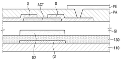
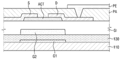
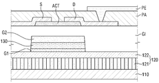
도 2는 도 1의 A-A' 영역의 수직 단면도이다.
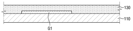
도 3은 본 발명의 다른 실시예에 따른 디스플레이 패널의 수직 단면도이다.
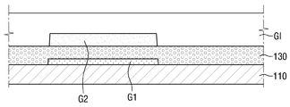
도 4는 본 발명의 다른 실시예에 따른 디스플레이 패널의 수직 단면도이다.
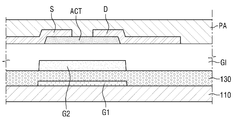
도 5는 본 발명의 다른 실시예에 따른 디스플레이 패널의 수직 단면도이다.
도 6 내지 도 14는 본 발명의 일 실시예에 따른 디스플레이 패널의 제조 공정별 단면도이다.
도 15 내지 도 23은 본 발명의 다른 실시예에 따른 디스플레이 패널의 제조 공정별 단면도이다.
도 24 내지 도 34는 본 발명의 다른 실시예에 따른 디스플레이 패널의 제조 공정별 단면도이다.
도 35 내지 도 45는 본 발명의 다른 실시예에 따른 디스플레이 패널의 제조 공정별 단면도이다.
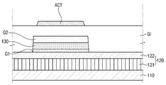
121: 전도성 와이어 패턴
122: 보호막
130: 절연층
Claims (16)
- 기판;
상기 기판 상에 형성되고 제1 방향으로 연장되는 게이트 라인;
상기 게이트 라인과 절연되고 제2 방향으로 연장되는 데이터 라인;
상기 게이트 라인 및 상기 데이터 라인과 전기적으로 연결되는 박막 트랜지스터; 및
상기 박막 트랜지스터와 전기적으로 연결되는 화소 전극을 포함하되,
상기 박막 트랜지스터는,
상기 기판 상에 형성되는 게이트 전극단;
상기 기판 및 상기 게이트 전극단 상에 형성되는 게이트 절연막;
상기 게이트 절연막 상에서, 상기 게이트 전극단과 적어도 일부 중첩되는 영역에 형성되는 액티브층; 및
상기 액티브층 및 상기 게이트 절연막 상에서, 서로 이격되어 형성되는 소스 전극 및 드레인 전극을 포함하고,
상기 게이트 전극단은 상기 기판 상에 형성되는 제1 게이트 전극, 상기 제1 게이트 전극 상에 형성되는 제2 게이트 전극 및 상기 제1 게이트 전극 및 상기 제2 게이트 전극 사이에 개재되는 절연층을 포함하며,
상기 제1 게이트 전극의 측면과 상기 절연층의 측면과 상기 제2 게이트 전극의 측면은 서로 정렬되고,
상기 제1 게이트 전극은 상기 제2 게이트 전극보다 반사율이 높은 디스플레이 패널. - 제 1 항에 있어서,
상기 제1 게이트 전극과 상기 제2 게이트 전극은 서로 전기적으로 절연인 디스플레이 패널. - 제 1 항에 있어서,
상기 게이트 라인은 상기 제2 게이트 전극과 전기적으로 연결되는 디스플레이 패널. - 제 1 항에 있어서,
상기 제1 게이트 전극의 두께는 상기 제2 게이트 전극의 두께보다 얇은 디스플레이 패널. - 제 1 항에 있어서,
상기 기판과 상기 게이트 라인 및 상기 박막 트랜지스터 사이에 편광판을 추가로 포함하는 디스플레이 패널. - 제 5 항에 있어서,
상기 편광판은 다수의 나란한 전도성 와이어 패턴을 포함하는 와이어 그리드 편광판인 디스플레이 패널. - 제 6 항에 있어서,
상기 와이어 그리드 편광판은 상기 전도성 와이어 패턴과 상기 게이트 라인 및 상기 박막 트랜지스터 사이에 전기 절연성인 보호막을 추가로 포함하는 디스플레이 패널. - 제 1 항에 있어서,
제1 게이트 전극의 두께는 10 nm 내지 100 nm 범위인 디스플레이 패널. - 기판 상에 제1 게이트 전극을 형성하는 단계;
상기 제1 게이트 전극 상에 절연층을 형성하는 단계;
상기 절연층 상에 제2 게이트 전극을 형성하는 단계;
상기 기판 및 제2 게이트 전극 상에 게이트 절연막을 형성하는 단계;
상기 게이트 절연막 상에서 상기 제2 게이트 전극과 적어도 일부 중첩되는 영역에 액티브층을 형성하는 단계;
상기 액티브층 상에서 서로 이격되는 위치에 소스 전극 및 드레인 전극을 형성하는 단계;
상기 게이트 절연막, 상기 액티브층, 상기 소스 전극 및 상기 드레인 전극 상에 상기 드레인 전극의 일부를 노출시키는 패시베이션 막을 형성하는 단계; 및
상기 노출된 드레인 전극과 전기적으로 연결되는 화소 전극을 형성하는 단계를 포함하고,
상기 제1 게이트 전극, 상기 절연층 및 상기 제2 게이트 전극은 동일한 마스크를 사용하여 형성하는 디스플레이 패널의 제조 방법. - 삭제
- 제 9 항에 있어서,
상기 제1 게이트 전극을 형성하는 단계는,
상기 기판 상에 와이어 그리드 편광판을 형성하는 단계; 및
상기 와이어 그리드 편광판 상에 상기 제1 게이트 전극을 형성하는 단계를 포함하는 디스플레이 패널의 제조 방법. - 제 11 항에 있어서,
상기 와이어 그리드 편광판을 형성하는 단계는,
상기 기판 상에 전도성 와이어 패턴을 형성하는 단계; 및
상기 전도성 와이어 패턴 상에 보호막을 형성하는 단계를 포함하는 디스플레이 패널의 제조 방법. - 기판 상에 제1 게이트 전극을 형성하는 단계;
상기 기판 및 상기 제1 게이트 전극 상에 절연층을 형성하는 단계;
상기 절연층 상에서 상기 제1 게이트 전극과 중첩되는 영역에 제2 게이트 전극을 형성하는 단계;
상기 절연층 및 제2 게이트 전극 상에 게이트 절연막을 형성하는 단계;
상기 게이트 절연막 상에서 상기 제2 게이트 전극과 적어도 일부 중첩되는 영역에 액티브층을 형성하는 단계;
상기 액티브층 상에서 서로 이격되는 위치에 소스 전극 및 드레인 전극을 형성하는 단계;
상기 게이트 절연막, 상기 액티브층, 상기 소스 전극 및 상기 드레인 전극 상에 상기 드레인 전극의 일부를 노출시키는 패시베이션 막을 형성하는 단계; 및
상기 노출된 드레인 전극과 전기적으로 연결되는 화소 전극을 형성하는 단계를 포함하고,
상기 제1 게이트 전극 및 상기 제2 게이트 전극은 동일한 마스크를 사용하여 형성하는 디스플레이 패널의 제조 방법. - 삭제
- 제 13 항에 있어서,
상기 제1 게이트 전극을 형성하는 단계는,
상기 기판 상에 와이어 그리드 편광판을 형성하는 단계; 및
상기 와이어 그리드 편광판 상에 상기 제1 게이트 전극을 형성하는 단계를 포함하는 디스플레이 패널의 제조 방법. - 제 15 항에 있어서,
상기 와이어 그리드 편광판을 형성하는 단계는,
상기 기판 상에 전도성 와이어 패턴을 형성하는 단계; 및
상기 전도성 와이어 패턴 상에 보호막을 형성하는 단계를 포함하는 디스플레이 패널의 제조 방법.
Priority Applications (4)
| Application Number | Priority Date | Filing Date | Title |
|---|---|---|---|
| KR1020140184549A KR102267126B1 (ko) | 2014-12-19 | 2014-12-19 | 디스플레이 패널 및 이의 제조 방법 |
| US14/813,556 US10319745B2 (en) | 2014-12-19 | 2015-07-30 | Display panel having improved brightness and method for fabricating the same |
| EP15179765.1A EP3035389B1 (en) | 2014-12-19 | 2015-08-05 | Display panel and method for fabricating the same |
| CN201510861984.7A CN105717718A (zh) | 2014-12-19 | 2015-12-01 | 具有提高的亮度的显示面板以及用于制造其的方法 |
Applications Claiming Priority (1)
| Application Number | Priority Date | Filing Date | Title |
|---|---|---|---|
| KR1020140184549A KR102267126B1 (ko) | 2014-12-19 | 2014-12-19 | 디스플레이 패널 및 이의 제조 방법 |
Publications (2)
| Publication Number | Publication Date |
|---|---|
| KR20160075938A KR20160075938A (ko) | 2016-06-30 |
| KR102267126B1 true KR102267126B1 (ko) | 2021-06-21 |
Family
ID=53776482
Family Applications (1)
| Application Number | Title | Priority Date | Filing Date |
|---|---|---|---|
| KR1020140184549A Active KR102267126B1 (ko) | 2014-12-19 | 2014-12-19 | 디스플레이 패널 및 이의 제조 방법 |
Country Status (4)
| Country | Link |
|---|---|
| US (1) | US10319745B2 (ko) |
| EP (1) | EP3035389B1 (ko) |
| KR (1) | KR102267126B1 (ko) |
| CN (1) | CN105717718A (ko) |
Families Citing this family (4)
| Publication number | Priority date | Publication date | Assignee | Title |
|---|---|---|---|---|
| CN108336144B (zh) * | 2018-01-22 | 2021-03-05 | 惠州市华星光电技术有限公司 | 一种用于显示面板中的薄膜晶体管及显示面板 |
| CN108417581B (zh) * | 2018-03-01 | 2021-09-28 | 厦门天马微电子有限公司 | 阵列基板、显示面板和显示装置 |
| CN109659371B (zh) * | 2018-12-21 | 2020-11-24 | 武汉华星光电技术有限公司 | 薄膜晶体管、薄膜晶体管的制作方法和液晶显示屏 |
| CN112909022B (zh) * | 2021-01-28 | 2022-09-09 | Tcl华星光电技术有限公司 | 阵列基板、其制造方法和显示装置 |
Citations (1)
| Publication number | Priority date | Publication date | Assignee | Title |
|---|---|---|---|---|
| JP2011227191A (ja) * | 2010-04-16 | 2011-11-10 | Hitachi Displays Ltd | 液晶表示装置 |
Family Cites Families (21)
| Publication number | Priority date | Publication date | Assignee | Title |
|---|---|---|---|---|
| KR100241721B1 (ko) | 1996-08-26 | 2000-02-01 | 구본준 | 액정표시소자 및 그 제조방법 |
| US6243199B1 (en) | 1999-09-07 | 2001-06-05 | Moxtek | Broad band wire grid polarizing beam splitter for use in the visible wavelength region |
| KR20030027302A (ko) | 2001-09-28 | 2003-04-07 | 삼성전자주식회사 | 저유전율 절연막을 사용하는 박막 트랜지스터 기판 및 그제조 방법 |
| US7123314B2 (en) | 2003-07-11 | 2006-10-17 | Nec Corporation | Thin-film transistor with set trap level densities, and method of manufactures |
| US7211825B2 (en) | 2004-06-14 | 2007-05-01 | Yi-Chi Shih | Indium oxide-based thin film transistors and circuits |
| EP2023169A4 (en) | 2006-04-07 | 2011-03-16 | Asahi Glass Co Ltd | WIRE GRILLE POLISHER AND METHOD FOR THE PRODUCTION THEREOF |
| KR101282323B1 (ko) * | 2006-10-26 | 2013-07-04 | 삼성디스플레이 주식회사 | 액정 표시 장치 |
| KR100817746B1 (ko) * | 2006-12-07 | 2008-03-31 | 한국전자통신연구원 | 다층 구조의 박막 트랜지스터 제조방법 및 상기 박막트랜지스터를 포함하는 능동 구동 표시 소자 |
| KR101414043B1 (ko) * | 2007-12-04 | 2014-07-21 | 삼성디스플레이 주식회사 | 박막 트랜지스터 기판 |
| JP5511157B2 (ja) * | 2008-07-03 | 2014-06-04 | キヤノン株式会社 | 発光表示装置 |
| CN101957530B (zh) * | 2009-07-17 | 2013-07-24 | 北京京东方光电科技有限公司 | Tft-lcd阵列基板及其制造方法 |
| EP2564247A2 (en) | 2010-04-27 | 2013-03-06 | The Regents Of The University Of Michigan | Display device having plasmonic color filters and photovoltaic capabilities |
| US20120057106A1 (en) | 2010-09-07 | 2012-03-08 | Electronics And Telecommunications Research Institute | Polarizer and liquid crystal display |
| KR101950824B1 (ko) * | 2011-11-25 | 2019-02-22 | 엘지디스플레이 주식회사 | 박막 트랜지스터 기판 및 이의 제조 방법 |
| KR20130116978A (ko) | 2012-04-17 | 2013-10-25 | 삼성디스플레이 주식회사 | 포토레지스트 조성물, 이를 이용한 편광자 제조방법 및 표시 기판의 제조방법 |
| KR101339001B1 (ko) * | 2012-07-04 | 2013-12-09 | 엘지디스플레이 주식회사 | 액정표시장치용 어레이기판 및 제조방법 |
| KR101977061B1 (ko) * | 2012-07-10 | 2019-05-13 | 삼성디스플레이 주식회사 | 편광 소자, 이를 포함하는 표시 패널 및 이의 제조 방법 |
| KR20140030382A (ko) | 2012-08-27 | 2014-03-12 | 삼성디스플레이 주식회사 | 액정 표시 장치 및 이의 제조 방법 |
| KR20140118027A (ko) | 2013-03-28 | 2014-10-08 | 삼성디스플레이 주식회사 | 액정표시장치 |
| KR20150005053A (ko) * | 2013-07-04 | 2015-01-14 | 삼성디스플레이 주식회사 | 어레이 기판 및 이를 포함하는 액정표시패널 |
| CN103531640A (zh) | 2013-11-01 | 2014-01-22 | 京东方科技集团股份有限公司 | 薄膜晶体管、阵列基板及其制造方法和显示装置 |
-
2014
- 2014-12-19 KR KR1020140184549A patent/KR102267126B1/ko active Active
-
2015
- 2015-07-30 US US14/813,556 patent/US10319745B2/en active Active
- 2015-08-05 EP EP15179765.1A patent/EP3035389B1/en active Active
- 2015-12-01 CN CN201510861984.7A patent/CN105717718A/zh active Pending
Patent Citations (1)
| Publication number | Priority date | Publication date | Assignee | Title |
|---|---|---|---|---|
| JP2011227191A (ja) * | 2010-04-16 | 2011-11-10 | Hitachi Displays Ltd | 液晶表示装置 |
Also Published As
| Publication number | Publication date |
|---|---|
| US10319745B2 (en) | 2019-06-11 |
| EP3035389B1 (en) | 2018-07-04 |
| US20160181281A1 (en) | 2016-06-23 |
| EP3035389A2 (en) | 2016-06-22 |
| EP3035389A3 (en) | 2016-09-07 |
| CN105717718A (zh) | 2016-06-29 |
| KR20160075938A (ko) | 2016-06-30 |
Similar Documents
| Publication | Publication Date | Title |
|---|---|---|
| US10095075B2 (en) | Display panel, display apparatus having the same and method of manufacturing the same | |
| US10790343B2 (en) | Display device | |
| US9842934B2 (en) | Array substrate and method of fabricating the same | |
| KR102180037B1 (ko) | 가요성 표시 장치 및 그 제조 방법 | |
| US9240485B2 (en) | Thin film transistor and method for manufacturing the same, array substrate and display device | |
| KR102366701B1 (ko) | 플렉서블 박막 트랜지스터 기판 및 플렉서블 유기 발광 표시 장치 | |
| US10288925B2 (en) | Liquid crystal display device and manufacturing method thereof | |
| US20140132903A1 (en) | Fringe field switching liquid crystal display device and method of fabricating the same | |
| US9519182B2 (en) | Display panel and method of manufacturing the same | |
| US9293522B2 (en) | Method of manufacturing capacitor and display apparatus including the same | |
| US9379147B2 (en) | Thin-film transistor array substrate and manufacturing method thereof | |
| US11996413B2 (en) | Thin film transistor and method of manufacturing the same, display substrate, and display device | |
| KR20160039080A (ko) | 유기 발광 표시 장치 | |
| KR102267126B1 (ko) | 디스플레이 패널 및 이의 제조 방법 | |
| US9673332B2 (en) | Circuit substrate manufacturing method | |
| KR102373687B1 (ko) | 표시장치 및 이의 제조방법 | |
| KR20200074591A (ko) | 고 해상도 마이크로 led 표시 장치 및 그 제조 방법 | |
| KR20160128518A (ko) | 표시장치 및 그 제조방법 | |
| KR20160125598A (ko) | 박막트랜지스터 어레이 기판 및 그의 제조방법, 박막트랜지스터 어레이 기판을 구비한 표시장치 | |
| US20160195760A1 (en) | Liquid crystal display apparatus | |
| KR102340409B1 (ko) | 표시 장치 | |
| US20070031642A1 (en) | Adhesive tape for a flexible display device and method of manufacturing a flexible display device using the same | |
| KR101960533B1 (ko) | 금속 산화물 반도체를 포함하는 박막 트랜지스터 기판 및 그 제조 방법 | |
| KR20160044168A (ko) | 표시 기판 및 이의 제조 방법 | |
| KR101648702B1 (ko) | 박막 트랜지스터 기판과 그 제조방법 및 액정표시장치와 그 제조방법 |
Legal Events
| Date | Code | Title | Description |
|---|---|---|---|
| PA0109 | Patent application |
Patent event code: PA01091R01D Comment text: Patent Application Patent event date: 20141219 |
|
| PG1501 | Laying open of application | ||
| A201 | Request for examination | ||
| PA0201 | Request for examination |
Patent event code: PA02012R01D Patent event date: 20191204 Comment text: Request for Examination of Application Patent event code: PA02011R01I Patent event date: 20141219 Comment text: Patent Application |
|
| E902 | Notification of reason for refusal | ||
| PE0902 | Notice of grounds for rejection |
Comment text: Notification of reason for refusal Patent event date: 20201224 Patent event code: PE09021S01D |
|
| E701 | Decision to grant or registration of patent right | ||
| PE0701 | Decision of registration |
Patent event code: PE07011S01D Comment text: Decision to Grant Registration Patent event date: 20210322 |
|
| GRNT | Written decision to grant | ||
| PR0701 | Registration of establishment |
Comment text: Registration of Establishment Patent event date: 20210615 Patent event code: PR07011E01D |
|
| PR1002 | Payment of registration fee |
Payment date: 20210615 End annual number: 3 Start annual number: 1 |
|
| PG1601 | Publication of registration | ||
| PR1001 | Payment of annual fee |
Payment date: 20240523 Start annual number: 4 End annual number: 4 |