KR102256421B1 - Integration of non-volatile charge trap memory devices and logic cmos devices - Google Patents
Integration of non-volatile charge trap memory devices and logic cmos devices Download PDFInfo
- Publication number
- KR102256421B1 KR102256421B1 KR1020207002501A KR20207002501A KR102256421B1 KR 102256421 B1 KR102256421 B1 KR 102256421B1 KR 1020207002501 A KR1020207002501 A KR 1020207002501A KR 20207002501 A KR20207002501 A KR 20207002501A KR 102256421 B1 KR102256421 B1 KR 102256421B1
- Authority
- KR
- South Korea
- Prior art keywords
- layer
- gate
- forming
- charge
- dielectric
- Prior art date
- Legal status (The legal status is an assumption and is not a legal conclusion. Google has not performed a legal analysis and makes no representation as to the accuracy of the status listed.)
- Active
Links
Images


Classifications
-
- H01L29/792—
-
- H—ELECTRICITY
- H10—SEMICONDUCTOR DEVICES; ELECTRIC SOLID-STATE DEVICES NOT OTHERWISE PROVIDED FOR
- H10D—INORGANIC ELECTRIC SEMICONDUCTOR DEVICES
- H10D30/00—Field-effect transistors [FET]
- H10D30/60—Insulated-gate field-effect transistors [IGFET]
- H10D30/69—IGFETs having charge trapping gate insulators, e.g. MNOS transistors
-
- B—PERFORMING OPERATIONS; TRANSPORTING
- B82—NANOTECHNOLOGY
- B82Y—SPECIFIC USES OR APPLICATIONS OF NANOSTRUCTURES; MEASUREMENT OR ANALYSIS OF NANOSTRUCTURES; MANUFACTURE OR TREATMENT OF NANOSTRUCTURES
- B82Y10/00—Nanotechnology for information processing, storage or transmission, e.g. quantum computing or single electron logic
-
- H01L21/8238—
-
- H01L29/7923—
-
- H—ELECTRICITY
- H10—SEMICONDUCTOR DEVICES; ELECTRIC SOLID-STATE DEVICES NOT OTHERWISE PROVIDED FOR
- H10B—ELECTRONIC MEMORY DEVICES
- H10B43/00—EEPROM devices comprising charge-trapping gate insulators
- H10B43/40—EEPROM devices comprising charge-trapping gate insulators characterised by the peripheral circuit region
-
- H—ELECTRICITY
- H10—SEMICONDUCTOR DEVICES; ELECTRIC SOLID-STATE DEVICES NOT OTHERWISE PROVIDED FOR
- H10D—INORGANIC ELECTRIC SEMICONDUCTOR DEVICES
- H10D30/00—Field-effect transistors [FET]
- H10D30/01—Manufacture or treatment
- H10D30/021—Manufacture or treatment of FETs having insulated gates [IGFET]
- H10D30/0212—Manufacture or treatment of FETs having insulated gates [IGFET] using self-aligned silicidation
-
- H—ELECTRICITY
- H10—SEMICONDUCTOR DEVICES; ELECTRIC SOLID-STATE DEVICES NOT OTHERWISE PROVIDED FOR
- H10D—INORGANIC ELECTRIC SEMICONDUCTOR DEVICES
- H10D30/00—Field-effect transistors [FET]
- H10D30/01—Manufacture or treatment
- H10D30/021—Manufacture or treatment of FETs having insulated gates [IGFET]
- H10D30/0413—Manufacture or treatment of FETs having insulated gates [IGFET] of FETs having charge-trapping gate insulators, e.g. MNOS transistors
-
- H—ELECTRICITY
- H10—SEMICONDUCTOR DEVICES; ELECTRIC SOLID-STATE DEVICES NOT OTHERWISE PROVIDED FOR
- H10D—INORGANIC ELECTRIC SEMICONDUCTOR DEVICES
- H10D30/00—Field-effect transistors [FET]
- H10D30/60—Insulated-gate field-effect transistors [IGFET]
- H10D30/69—IGFETs having charge trapping gate insulators, e.g. MNOS transistors
- H10D30/691—IGFETs having charge trapping gate insulators, e.g. MNOS transistors having more than two programming levels
-
- H—ELECTRICITY
- H10—SEMICONDUCTOR DEVICES; ELECTRIC SOLID-STATE DEVICES NOT OTHERWISE PROVIDED FOR
- H10D—INORGANIC ELECTRIC SEMICONDUCTOR DEVICES
- H10D30/00—Field-effect transistors [FET]
- H10D30/60—Insulated-gate field-effect transistors [IGFET]
- H10D30/69—IGFETs having charge trapping gate insulators, e.g. MNOS transistors
- H10D30/693—Vertical IGFETs having charge trapping gate insulators
-
- H—ELECTRICITY
- H10—SEMICONDUCTOR DEVICES; ELECTRIC SOLID-STATE DEVICES NOT OTHERWISE PROVIDED FOR
- H10D—INORGANIC ELECTRIC SEMICONDUCTOR DEVICES
- H10D64/00—Electrodes of devices having potential barriers
- H10D64/01—Manufacture or treatment
- H10D64/031—Manufacture or treatment of data-storage electrodes
- H10D64/037—Manufacture or treatment of data-storage electrodes comprising charge-trapping insulators
-
- H—ELECTRICITY
- H10—SEMICONDUCTOR DEVICES; ELECTRIC SOLID-STATE DEVICES NOT OTHERWISE PROVIDED FOR
- H10D—INORGANIC ELECTRIC SEMICONDUCTOR DEVICES
- H10D84/00—Integrated devices formed in or on semiconductor substrates that comprise only semiconducting layers, e.g. on Si wafers or on GaAs-on-Si wafers
- H10D84/01—Manufacture or treatment
- H10D84/0123—Integrating together multiple components covered by H10D12/00 or H10D30/00, e.g. integrating multiple IGBTs
- H10D84/0126—Integrating together multiple components covered by H10D12/00 or H10D30/00, e.g. integrating multiple IGBTs the components including insulated gates, e.g. IGFETs
- H10D84/0165—Integrating together multiple components covered by H10D12/00 or H10D30/00, e.g. integrating multiple IGBTs the components including insulated gates, e.g. IGFETs the components including complementary IGFETs, e.g. CMOS devices
-
- H—ELECTRICITY
- H10—SEMICONDUCTOR DEVICES; ELECTRIC SOLID-STATE DEVICES NOT OTHERWISE PROVIDED FOR
- H10D—INORGANIC ELECTRIC SEMICONDUCTOR DEVICES
- H10D30/00—Field-effect transistors [FET]
- H10D30/60—Insulated-gate field-effect transistors [IGFET]
- H10D30/601—Insulated-gate field-effect transistors [IGFET] having lightly-doped drain or source extensions, e.g. LDD IGFETs or DDD IGFETs
-
- H—ELECTRICITY
- H10—SEMICONDUCTOR DEVICES; ELECTRIC SOLID-STATE DEVICES NOT OTHERWISE PROVIDED FOR
- H10D—INORGANIC ELECTRIC SEMICONDUCTOR DEVICES
- H10D62/00—Semiconductor bodies, or regions thereof, of devices having potential barriers
- H10D62/10—Shapes, relative sizes or dispositions of the regions of the semiconductor bodies; Shapes of the semiconductor bodies
- H10D62/117—Shapes of semiconductor bodies
- H10D62/118—Nanostructure semiconductor bodies
- H10D62/119—Nanowire, nanosheet or nanotube semiconductor bodies
- H10D62/122—Nanowire, nanosheet or nanotube semiconductor bodies oriented at angles to substrates, e.g. perpendicular to substrates
Landscapes
- Engineering & Computer Science (AREA)
- Chemical & Material Sciences (AREA)
- Nanotechnology (AREA)
- Physics & Mathematics (AREA)
- Mathematical Physics (AREA)
- Theoretical Computer Science (AREA)
- Crystallography & Structural Chemistry (AREA)
- Non-Volatile Memory (AREA)
- Semiconductor Memories (AREA)
- Metal-Oxide And Bipolar Metal-Oxide Semiconductor Integrated Circuits (AREA)
- Thin Film Transistor (AREA)
Abstract
비-휘발성 메모리 디바이스를 로직 MOS 흐름으로 집적하는 방법의 일 실시예가 설명된다. 일반적으로 방법은: 기판의 제 1 구역에 기판의 표면을 오버라잉(overlying)하는 반도체 재료로부터 메모리 디바이스의 채널을 형성하는 단계를 포함하고, 채널은 메모리 디바이스의 소스 및 드레인을 접속하며; 채널의 복수의 표면들 근처의 채널 위에 전하 트랩핑 유전체 스택을 형성하는 단계를 포함하며, 전하 트랩핑 유전체 스택은 터널링 층 위에 전하 트랩핑 층 상에 블로킹 층을 포함하며; 및 상기 기판의 제 2 구역 위에 MOS 디바이스를 형성하는 단계를 포함한다.One embodiment of a method of integrating a non-volatile memory device into a logic MOS flow is described. The method generally includes: forming a channel of a memory device from a semiconductor material overlying a surface of the substrate in a first region of the substrate, the channel connecting a source and a drain of the memory device; Forming a charge trapping dielectric stack over the channel near the plurality of surfaces of the channel, the charge trapping dielectric stack comprising a blocking layer over the charge trapping layer over the tunneling layer; And forming a MOS device over the second region of the substrate.
Description
[0001] 본 출원은 2007년 5월 25일에 출원된 미국 가 특허 출원 일련번호 제 60/940,137 호 및 2007년 5월 25일에 출원된 미국 가 특허 출원 일련번호 제 60/940,148 호에 대해 35 U.S.C. 119(e)하의 우선권의 이익을 주장하는 2012년 1월 10일에 현재 발행된 미국 특허 번호 제 8,093,128 호인, 2008년 5월 22일에 출원된 미국 출원 일련번호 제 12/125,864 호의 연속인, 2008년 8월 4일에 출원된 공동-계류중인 미국 출원 일련번호 제 12/185,751 호의 부분 연속 출원이며, 이들 모두는 본원에 인용에 의해 포함된다.[0001] This application is based on US provisional patent application serial number 60/940,137 filed on May 25, 2007 and US provisional patent application serial number 60/940,148 filed on May 25, 2007. USC U.S. Patent No. 8,093,128, currently issued on January 10, 2012, claiming the benefit of priority under 119(e), continuation of U.S. Application Serial No. 12/125,864 filed May 22, 2008, 2008 It is a partial continuation application of co-pending U.S. Application Serial No. 12/185,751, filed Aug. 4,, all of which are incorporated herein by reference.
[0002] 본 발명은 반도체 디바이스들의 분야에 관한 것으로, 더 구체적으로 로직 CMOS 디바이스들로 집적되는 비-휘발성 전하 트랩 메모리 디바이스들에 관한 것이다.[0002] The present invention relates to the field of semiconductor devices, and more particularly to non-volatile charge trap memory devices that are integrated into logic CMOS devices.
[0003] 집적된 회로들에서의 피처(feature) 스케일링은 더 유능한 전자 디바이스들을 가능하게 한다. 더 작은 피처들로의 스케일링은 정해진 형태 팩터에서의 기능적 유닛들의 밀도들을 증가시킬뿐 아니라 디바이스 프로세싱 속도들을 증가시킨다. 그러나, 디바이스 스케일링은 쟁점 없이 이루어지지 않는다. 예를 들어, 더 작은 디바이스들의 성능을 최적화하는 것은 점점더 어려워지고 있다. 이것은 디바이스들이 스케일됨에 따라 데이터 유지 및 센싱이 점점더 어려워지는 비휘발성 전하 트랩 메모리 디바이스들의 스케일링에 대해 더 그러하다.Feature scaling in integrated circuits enables more capable electronic devices. Scaling to smaller features increases device processing speeds as well as increases the densities of functional units in a given shape factor. However, device scaling is not without issues. For example, optimizing the performance of smaller devices is becoming increasingly difficult. This is more so for the scaling of non-volatile charge trap memory devices, where data retention and sensing becomes increasingly difficult as the devices scale.
[0004] 디바이스 스케일링에 더하여, 시스템-온-칩(system-on-an-chip) 타입 아키텍처는 또한 전자 디바이스 기능을 증가시킨다. 그와 같은 아키텍처는 예를 들어, 제조 비용을 감소시킬뿐 아니라 메모리와 로직 디바이스들 사이의 통신 대역폭을 증가시키기 위해 로직 디바이스에서와 동일한 기판상에 메모리 디바이스를 통합할 수 있다.In addition to device scaling, a system-on-an-chip type architecture also increases electronic device functionality. Such an architecture can, for example, integrate the memory device on the same substrate as the logic device to reduce manufacturing cost as well as increase the communication bandwidth between the memory and the logic devices.
[0005] 로직 MOS 디바이스를 위한 제조 프로세스가 메모리 디바이스의 제조 프로세스를 방해할 수 있으며 그 반대도 마찬가지이기 때문에 시스템-온-칩 아키텍처에서의 이들 비유사한 디바이스들의 집적은 문제가 있다. 그와 같은 딜레마(dilemma)는 예를 들어, 메모리 디바이스를 위한 유전체 스택의 제조로 로직 MOS 게이트 산화물 프로세스 모듈을 집적할 때 발생할 수 있다. 또한, 로직 디바이스들을 위한 채널 및 웰 임플란트 프로세싱은 또한 후자의 형성이 전자에 대해 문제가 될 수 있는 동안 메모리 디바이스 유전체 스택에 장해가 될 수 있다. 또 다른 예로서, 로직 트랜지스터를 위해 유용한 실리사이드된 컨택트들은 비휘발성 전하 트랩 메모리 디바이스에 불리하게 영향을 미칠 수 있다.Integration of these dissimilar devices in a system-on-chip architecture is problematic because the manufacturing process for a logic MOS device can interfere with the manufacturing process of a memory device and vice versa. Such a dilemma can arise, for example, when integrating a logic MOS gate oxide process module into the fabrication of a dielectric stack for a memory device. In addition, channel and well implant processing for logic devices can also be detrimental to the memory device dielectric stack while the latter formation can be an issue for the former. As another example, silicided contacts useful for logic transistors can adversely affect nonvolatile charge trap memory devices.
[0006] 또한, 비-휘발성 메모리 디바이스의 동작은 비교적 높은 전압들(HV), 전형적으로 적어도 10V의 적용을 요구할 수 있다. 그러나, 스케일된 로직 디바이스의 제조시에 사용되는 종래의 프로세스들은 5 V 또는 그 이하에서의 디바이스 동작을 위해 최적화된다. 그와 같은 낮은 전압 디바이스들은 메모리 디바이스와 직접 인터페이싱하기 위해 충분히 높은 브레이크다운(breakdown) 전압을 결여할 수 있다.Further, operation of a non-volatile memory device may require application of relatively high voltages (HV), typically at least 10V. However, conventional processes used in the manufacture of scaled logic devices are optimized for device operation at 5V or less. Such low voltage devices may lack a breakdown voltage high enough to directly interface with the memory device.
[0007] 본 발명의 실시예들은 제한이 아닌 예시로서, 첨부하는 도면들의 도면에서 예시된다:
[0008] 도 1은 본 발명의 특정 실시예들에 따른, 로직 MOS 제조 프로세스로 집적되는 비-휘발성 전하 트랩 메모리 디바이스의 제조 프로세스에서 사용되는 특정 모듈들의 시퀀스들을 도시하는 흐름도를 예시한다;
[0009] 도 2a 및 2b는 본 발명의 특정 실시예들에 따른, 도 1에 예시되는 특정 모듈들을 구현하기 위한 비휘발성 전하-트랩핑 유전체 스택으로의 로직 MOS 게이트 제조의 집적에서 특정 동작들의 시퀀스들을 도시하는 흐름도를 예시한다; 그리고
[0010] 도 3a는 본 발명의 일 실시예에 따른, 스크리닝(screening) 산화물이 기판의 MOS 및 HV MOS 구역들 위에 있는 동안 SONOS 채널 임플란트가 수행되는 반도체 구조의 형성에서의 동작들을 나타내는 단면도를 예시한다;
[0011] 도 3b는 본 발명의 일 실시예에 따른, 제 1 게이트 절연체 층을 형성하기 위한 준비로 SONOS 전하 트랩핑 유전체 스택이 형성되며 MOS 및 HV MOS 구역들이 클리닝(cleaning)되는 반도체 구조의 형성에서의 동작들을 나타내는 단면도를 예시한다;
[0012] 도 3c는 본 발명의 일 실시예에 따른, 제 1 게이트 절연체 층이 MOS 및 HV MOS 구역들 위에 형성되는 반도체 구조의 형성에서의 동작들을 나타내는 단면도를 예시한다;
[0013] 도 3d는 본 발명의 일 실시예에 따른, 제 2 게이트 절연체 층을 형성하기 위해 MOS 구역에서의 제 1 게이트 절연체 층이 기판의 제 3 구역에서 개방되는 동안 SONOS 및 HV MOS 디바이스 구역들이 마스킹되는 동작들을 나타내는 단면도를 예시한다;
[0014] 도 3e는 본 발명의 일 실시예에 따른, 제 2 게이트 절연체 층이 MOS 구역에 형성되는 반도체 구조의 형성에서의 동작들을 나타내는 단면도를 예시한다;
[0015] 도 3f는 본 발명의 일 실시예에 따른, SONOS 산화물 블로킹 층, HV MOS 게이트 절연체 층 및 MOS 게이트 절연체 층이 질화되는 반도체 구조의 형성에서의 동작들을 나타내는 단면도를 예시한다;
[0016] 도 3g는 본 발명의 일 실시예에 따른, 게이트 층이 증착되는 반도체 구조의 형성에서의 동작들을 나타내는 단면도를 예시한다;
[0017] 도 3h는 본 발명의 일 실시예에 따른, 게이트 전극이 형성되는 반도체 구조의 형성에서의 동작들을 나타내는 단면도를 예시한다;
[0018] 도 3i는 본 발명의 일 실시예에 따른, 측벽 스페이서가 형성되는 반도체 구조의 형성에서의 동작들을 나타내는 단면도를 예시한다; 그리고
[0019] 도 3j는 본 발명의 일 실시예에 따른, 게이트 스택들의 한정을 완료하기 위해 측벽 스페이서들 근처의 전하 트랩 유전체 및 게이트 유전체가 제거되는 반도체 구조의 형성에서의 동작들을 나타내는 단면도를 예시한다.
[0020] 도 4a는 본 발명의 일 실시예에 따른, 측벽 스페이서들을 갖는 SONOS 게이트 스택뿐 아니라 단일 기판상의 근처의 측벽 스페이서들을 갖는 HV MOS 및 MOS 디바이스 게이트 스택들을 갖는 반도체 구조의 형성에서의 동작들을 나타내는 단면도를 예시한다;
[0021] 도 4b는 본 발명의 일 실시예에 따른, 멀티-층된 라이너가 SONOS 및 로직 디바이스들 위에 증착되는 반도체 구조의 형성에서의 동작들을 나타내는 단면도를 예시한다;
[0022] 도 4c는 본 발명의 일 실시예에 따른, 1회용 스페이서를 형성하기 위해 멀티-층된 라이너의 최상부 층이 에칭되는 반도체 구조의 형성에서의 동작들을 나타내는 단면도를 예시한다;
[0023] 도 4d는 본 발명의 일 실시예에 따른, SONOS 및 MOS 디바이스들이 마스킹되는 동안 HV MOS 디바이스가 소스 및 드레인 임플란트를 수신하는 반도체 구조의 형성에서의 동작들을 나타내는 단면도를 예시한다;
[0024] 도 4e는 본 발명의 일 실시예에 따른, 1회용 스페이서가 SONOS 및 로직 디바이스들로부터 제거되는 반도체 구조의 형성에서의 동작들을 나타내는 단면도를 예시한다;
[0025] 도 4f는 본 발명의 일 실시예에 따른, 멀티층된 라이너가 MOS 디바이스로부터 제거되지만 SONOS 및 HV MOS 디바이스 위에 유지되는 반도체 구조의 형성에서의 동작들을 나타내는 단면도를 예시한다;
[0026] 도 4g는 본 발명의 일 실시예에 따른, 실리사이드가 MOS 디바이스 상에 형성되지만 SONOS 및 MOS 디바이스들 위에 멀티-층된 라이너의 바닥 층에 의해 블로킹되는 반도체 구조의 형성에서의 동작들을 나타내는 단면도를 예시한다;
[0027] 도 5는 본 발명의 일 실시예에 따른, 층간 유전체(interlayer dielectric: ILD) 층이 MOS SONOS 및 HV MOS 게이트 스택들 근처의 측벽 스페이서들의 측벽들 상에 형성되는 반도체 구조의 형성에서의 동작들을 나타내는 단면도를 예시한다;
[0028] 도 6a는 본 발명의 일 실시예에 따른, 스트레스 유도 ILD 층이 MOS 게이트 스택 근처의 측벽 스페이서들 상에 형성되며 SONOS 및 HV MOS 게이트 스택들 위에 멀티-층된 라이너의 바닥 층 상에 형성되는 반도체 구조의 형성에서의 동작들을 나타내는 단면도를 예시한다;
[0029] 도 6b는 본 발명의 일 실시예에 따른, 낮은-스트레스 ILD 층이 SONOS 및 HV MOS 게이트 스택들 근처의 측벽 스페이서들을 커버하는 멀티-층된 라이너의 바닥 층 상에 형성되며 그리고 MOS 디바이스 위에 스트레스 유도 ILD 층 상에 형성되는 반도체 구조의 형성에서의 동작들을 나타내는 단면도를 예시한다;
[0030] 도 7a는 분열 전하-트랩핑 구역을 포함하는 비-평면 멀티게이트 디바이스를 예시한다;
[0031] 도 7b는 도 7a의 비-평면 멀티게이트 디바이스의 단면도를 예시한다;
[0032] 도 7c는 도 7a의 비-평면 멀티게이트 디바이스들의 수직 스트링의 단면도를 예시한다;
[0033] 도 8은 로직 디바이스로 집적되는 비-평면 멀티게이트 디바이스를 제조하는데 사용되는 특정 모듈들의 시퀀스들을 도시하는 흐름도를 예시한다;
[0034] 도 9a 및 9b는 분열 전하-트랩핑 구역 및 수평 나노와이어(nanowire) 채널을 포함하는 비-평면 멀티게이트 디바이스를 예시한다;
[0035] 도 9c는 도 9a의 비-평면 멀티게이트 디바이스들의 수직 스트링의 단면도를 예시한다;
[0036] 도 10a 및 10b는 분열 전하-트랩핑 구역 및 수직 나노와이어 채널을 포함하는 비-평면 멀티게이트 디바이스를 예시한다;
[0037] 도 11a 내지 11f는 도 10a의 비-평면 멀티게이트 디바이스를 제조하기 위한 게이트 제 1 방식을 예시한다; 그리고
[0038] 도 12a 내지 12f는 도 10a의 비-평면 멀티게이트 디바이스를 제조하기 위한 게이트 최종 방식을 예시한다.[0007] Embodiments of the present invention are illustrated in the drawings of the accompanying drawings by way of example, not limitation:
[0008] FIG. 1 illustrates a flow diagram showing sequences of specific modules used in a manufacturing process of a non-volatile charge trap memory device integrated into a logic MOS manufacturing process, according to certain embodiments of the present invention;
2A and 2B illustrate a sequence of specific operations in the integration of fabrication of a logic MOS gate into a nonvolatile charge-trapping dielectric stack for implementing the specific modules illustrated in FIG. 1, according to certain embodiments of the present invention. Illustrate a flow chart showing them; And
3A is an illustration of a cross-sectional view showing operations in formation of a semiconductor structure in which a SONOS channel implant is performed while a screening oxide is over the MOS and HV MOS regions of the substrate, according to an embodiment of the present invention. do;
[0011] FIG. 3B shows the formation of a semiconductor structure in which a SONOS charge trapping dielectric stack is formed and MOS and HV MOS regions are cleaned in preparation for forming a first gate insulator layer according to an embodiment of the present invention. Illustrates a cross-sectional view showing the operations in;
3C illustrates a cross-sectional view showing operations in formation of a semiconductor structure in which a first gate insulator layer is formed over MOS and HV MOS regions, according to an embodiment of the present invention;
3D shows the SONOS and HV MOS device regions while the first gate insulator layer in the MOS region is opened in the third region of the substrate to form a second gate insulator layer, according to an embodiment of the present invention. Illustrates a cross-sectional view showing operations being masked;
3E illustrates a cross-sectional view showing operations in formation of a semiconductor structure in which a second gate insulator layer is formed in a MOS region, according to an embodiment of the present invention;
3F illustrates a cross-sectional view showing operations in formation of a semiconductor structure in which a SONOS oxide blocking layer, an HV MOS gate insulator layer, and a MOS gate insulator layer are nitrided, in accordance with an embodiment of the present invention;
3G illustrates a cross-sectional view showing operations in formation of a semiconductor structure in which a gate layer is deposited, in accordance with an embodiment of the present invention;
3H illustrates a cross-sectional view showing operations in formation of a semiconductor structure in which a gate electrode is formed, according to an embodiment of the present invention;
3I illustrates a cross-sectional view showing operations in formation of a semiconductor structure in which sidewall spacers are formed, according to an embodiment of the present invention; And
3J illustrates a cross-sectional view showing operations in the formation of a semiconductor structure in which the gate dielectric and the charge trap dielectric near the sidewall spacers are removed to complete the definition of the gate stacks, according to an embodiment of the present invention. .
4A illustrates operations in the formation of a semiconductor structure with HV MOS and MOS device gate stacks with sidewall spacers adjacent on a single substrate as well as a SONOS gate stack with sidewall spacers, according to an embodiment of the present invention. Illustratively shows the cross-sectional view;
4B illustrates a cross-sectional view illustrating operations in formation of a semiconductor structure in which a multi-layered liner is deposited over SONOS and logic devices, in accordance with an embodiment of the present invention;
4C illustrates a cross-sectional view showing operations in formation of a semiconductor structure in which the top layer of a multi-layered liner is etched to form a disposable spacer, according to an embodiment of the present invention;
4D illustrates a cross-sectional view showing operations in formation of a semiconductor structure in which an HV MOS device receives source and drain implants while SONOS and MOS devices are masked, according to an embodiment of the present invention;
4E illustrates a cross-sectional view showing operations in formation of a semiconductor structure in which a disposable spacer is removed from SONOS and logic devices, in accordance with an embodiment of the present invention;
[0025] FIG. 4F illustrates a cross-sectional view showing operations in formation of a semiconductor structure in which a multilayered liner is removed from the MOS device but retained over the SONOS and HV MOS device, according to an embodiment of the present invention;
4G is a cross-sectional view showing operations in the formation of a semiconductor structure in which silicide is formed on a MOS device but is blocked by a bottom layer of a multi-layered liner over SONOS and MOS devices, according to an embodiment of the present invention. Exemplify;
[0027] FIG. 5 shows in the formation of a semiconductor structure in which an interlayer dielectric (ILD) layer is formed on sidewalls of sidewall spacers near MOS SONOS and HV MOS gate stacks, according to an embodiment of the present invention. Illustrates a cross-sectional view showing operations;
6A shows a stress inducing ILD layer is formed on the sidewall spacers near the MOS gate stack and is formed on the bottom layer of the multi-layered liner over the SONOS and HV MOS gate stacks according to an embodiment of the present invention. Illustrates a cross-sectional view showing operations in the formation of a semiconductor structure to be formed;
6B shows a low-stress ILD layer is formed on the bottom layer of a multi-layered liner covering sidewall spacers near SONOS and HV MOS gate stacks and over the MOS device, according to an embodiment of the present invention. Illustrates a cross-sectional view showing operations in formation of a semiconductor structure formed on a stress inducing ILD layer;
7A illustrates a non-planar multigate device comprising a split charge-trapping region;
7B illustrates a cross-sectional view of the non-planar multigate device of FIG. 7A;
7C illustrates a cross-sectional view of a vertical string of non-planar multigate devices of FIG. 7A;
[0033] FIG. 8 illustrates a flow diagram showing sequences of specific modules used to fabricate a non-planar multigate device that is integrated into a logic device;
9A and 9B illustrate a non-planar multigate device comprising a split charge-trapping region and a horizontal nanowire channel;
9C illustrates a cross-sectional view of a vertical string of non-planar multigate devices of FIG. 9A;
10A and 10B illustrate a non-planar multigate device comprising a split charge-trapping region and a vertical nanowire channel;
[0037] Figures 11A-11F illustrate a gate first scheme for fabricating the non-planar multigate device of Figure 10A; And
12A-12F illustrate the gate final scheme for fabricating the non-planar multigate device of FIG. 10A.
[0039] 로직 디바이스들로 집적되는 비-휘발성 전하 트랩 메모리 디바이스의 실시예들은 도면들을 참조하여 본원에 설명된다. 그러나, 특정 실시예들은 이들 특정 상세들 중 하나 또는 그 초과 없이, 또는 다른 알려진 방법들, 재료들 및 장치들과 조합하여 실시될 수 있다. 다음의 설명에서, 본 발명의 완전한 이해를 제공하기 위해 특정 재료들, 치수들 및 프로세스 파라미터들 등과 같은 수많은 특정 상세들이 설명된다. 다른 사례들에서, 잘-알려진 반도체 설계 및 제조 기술들은 본 발명을 불필요하게 모호하게 하는 것을 회피하기 위해 특히 상세하게 설명되지 않는다. 본 명세서 전반에 인용되는 "실시예"는 그 실시예와 관련하여 설명되는 특정 피처, 구조, 재료 또는 특성이 본 발명의 적어도 하나의 실시예에 포함되는 것을 의미한다. 따라서, 본 명세서 전반의 다양한 장소들에서 어구 "일 실시예에서"의 표현들은 반드시 본 발명의 동일한 실시예를 지칭하는 것은 아니다. 더욱이, 특정 피처들, 재료들 또는 특성들은 하나 또는 그 초과의 실시예들에서 임의의 적합한 방식으로 조합될 수 있다.Embodiments of a non-volatile charge trap memory device integrated into logic devices are described herein with reference to the drawings. However, certain embodiments may be practiced without one or more of these specific details, or in combination with other known methods, materials and devices. In the following description, numerous specific details are set forth, such as specific materials, dimensions and process parameters, etc. to provide a thorough understanding of the present invention. In other instances, well-known semiconductor design and fabrication techniques have not been described in particular detail in order to avoid unnecessarily obscuring the present invention. “An embodiment” as recited throughout this specification means that a particular feature, structure, material, or characteristic described in connection with the embodiment is included in at least one embodiment of the present invention. Thus, the expressions of the phrase “in one embodiment” in various places throughout this specification are not necessarily referring to the same embodiment of the invention. Moreover, certain features, materials or properties may be combined in any suitable manner in one or more embodiments.
[0040] 본원에 이용된 바와 같은 용어들 "위에(over)", "아래(under)", "사이에(between)" 및 "상에(on)"는 다른 층들에 관한 하나의 층의 상대적인 포지션을 지칭한다. 그와 같이, 예를 들어, 다른 층 위에 또는 아래에 증착되거나 배치되는 하나의 층은 다른 층과 직접 접촉할 수 있거나 하나 또는 그 초과의 개재하는 층들을 가질 수 있다. 더욱이, 층들 사이에 증착되거나 배치되는 하나의 층은 그 층들과 직접 접촉할 수 있거나 하나 또는 그 초과의 개재하는 층들을 가질 수 있다. 반대로, 제 2 층 "상의" 제 1 층은 제 2 층과 접촉한다. 추가로, 다른 층들에 관한 하나의 층의 상대적 포지션은 동작들이 기판의 절대 배향의 고려 없이 시작하는 기판에 대하여 막들을 증착, 수정 및 제거하는 것을 가정하여 제공된다.[0040] The terms "over", "under", "between" and "on" as used herein refer to the relative Refers to the position. As such, for example, one layer deposited or disposed above or below another layer may be in direct contact with another layer or may have one or more intervening layers. Moreover, a layer deposited or disposed between layers may be in direct contact with the layers or may have one or more intervening layers. Conversely, the first layer “on” the second layer contacts the second layer. Additionally, the relative position of one layer with respect to other layers is provided assuming that operations deposit, modify and remove films relative to the starting substrate without consideration of the absolute orientation of the substrate.
[0041] 일 실시예에서, SONOS 스택과 같은 비휘발성 전하 트랩 유전체 스택은 로직 MOS 디바이스들의 웰 및 채널 임플란트들 중 적어도 일부가 기판의 제 2 구역에 형성된 후에 기판의 제 1 구역에 형성된다.In one embodiment, a non-volatile charge trap dielectric stack, such as a SONOS stack, is formed in the first region of the substrate after at least some of the well and channel implants of the logic MOS devices are formed in the second region of the substrate.
[0042] 다른 실시예에서, 비휘발성 전하 트랩 유전체 스택은 임의의 로직 MOS 게이트 산화 프로세싱 이전에 형성된다. 하나의 그와 같은 실시예에서, SONOS 스택은 기판의 제 2 구역으로부터 제거되며, 그리고 열적 산화는 반도체 기판의 제 2 구역 위에 제 1 게이트 절연체 층을 형성하며 그리고 SONOS 스택의 블로킹 층을 열적으로 재산화시킨다. 추가적인 실시예에서, 질화 프로세스는 제 1 게이트 절연체 층 및 블로킹 층을 동시에 질화시킨다.In another embodiment, the non-volatile charge trap dielectric stack is formed prior to any logic MOS gate oxidation processing. In one such embodiment, the SONOS stack is removed from the second region of the substrate, and thermal oxidation forms a first gate insulator layer over the second region of the semiconductor substrate and thermally property the blocking layer of the SONOS stack. Make it angry. In a further embodiment, the nitridation process simultaneously nitrates the first gate insulator layer and the blocking layer.
[0043] 다른 실시예에서, 실리사이드 컨택트들이 없는 비휘발성 전하 트랩 메모리 디바이스는 실리사이드 컨택트들을 갖는 로직 디바이스로 집적된다. 그와 같은 실시예는 메모리 디바이스에서의 실리사이드-관련된 스트레스를 감소시킴으로써 비휘발성 전하 트랩 메모리 디바이스의 신뢰성을 유용하게 개선할 수 있다.In another embodiment, a nonvolatile charge trap memory device without silicide contacts is integrated into a logic device with silicide contacts. Such an embodiment can advantageously improve the reliability of a nonvolatile charge trap memory device by reducing the silicide-related stress in the memory device.
[0044] 추가적인 실시예에서, 로직 디바이스들 중 적어도 하나는 HV 동작(예를 들어, 10 V보다 큰 브레이크다운 전압)을 허용하기 위해 로직 디바이스들 중 적어도 다른 하나보다 더 긴 저농도 도핑된 소스 및 드레인(즉, 오프셋 소스 및 드레인)을 갖는다. 하나의 그와 같은 실시예에서, 로직 디바이스들은 HV PMOS 디바이스 및 n-타입 MOS(NMOS) 디바이스를 포함하며, NMOS 디바이스는 HV PMOS 디바이스에서보다 더 작은 소스 및 드레인 오프셋을 갖는다. 다른 그와 같은 실시예에서, 로직 디바이스들은 HV PMOS 디바이스 및 PMOS 디바이스를 포함하며, PMOS 디바이스는 HV PMOS 디바이스에서보다 더 작은 소스 및 드레인 오프셋을 갖는다. 특정 실시예에서, HV MOS 디바이스의 저농도 도핑된 소스 및 드레인은 MOS 디바이스의 게이트 스택의 측벽 근처에 측벽 스페이서의 두께보다 더 큰 길이이다.[0044] In a further embodiment, at least one of the logic devices is a lightly doped source and drain longer than at least another of the logic devices to allow HV operation (eg, a breakdown voltage greater than 10 V). (Ie, offset source and drain). In one such embodiment, the logic devices include HV PMOS devices and n-type MOS (NMOS) devices, which NMOS devices have smaller source and drain offsets than in HV PMOS devices. In another such embodiment, the logic devices include HV PMOS devices and PMOS devices, which PMOS devices have smaller source and drain offsets than in HV PMOS devices. In certain embodiments, the heavily doped source and drain of the HV MOS device are of a length greater than the thickness of the sidewall spacers near the sidewalls of the gate stack of the MOS device.
[0045] 다른 실시예에서, HV MOS 소스 및 드레인을 오프셋하기 위해 그리고 또한 실리사이드화로부터 비휘발성 전하 트랩 메모리 디바이스를 보호하기 위해 멀티-층된 라이너가 사용된다. 하나의 그와 같은 실시예에서, 멀티-층된 라이너는 적어도 최상부 및 바닥 층을 포함하며, 최상부 층은 HV MOS 소스 및 드레인을 오프셋하기 위해 1회용 스페이서로 형성되며 바닥 층은 로직 디바이스들 중 하나 또는 그 초과의 실리사이드화 동안 비휘발성 전하 트랩 메모리 디바이스를 마스크하도록 이용된다. 다른 실시예에서, 바닥 층은 로직 디바이스들 중 하나 또는 그 초과의 실리사이드화 동안 HV MOS 디바이스를 마스킹하도록 추가로 이용된다. 특정 실시예에서, HV MOS 소스 및 드레인이 임플란트된 후에 1회용 스페이서가 멀티-층된 라이너의 바닥 층에 대해 선택적으로 제거된다. 추가적인 실시예에서, 멀티-층된 라이너의 바닥 층은 ILD 층으로서 비휘발성 전하 트랩 메모리 디바이스 위에 유지되며, 다른 ILD 층으로 커버되며, 그 후에 접촉 형성 동안을 통해 에칭된다. 다른 실시예에서, 멀티-층된 라이너의 바닥 층은 ILD 층으로서 비휘발성 전하 트랩 메모리 디바이스 및 HV MOS 디바이스 위에 유지된다. 하나의 그와 같은 실시예에서, 멀티-층된 라이너의 바닥 층에서의 스트레스는 바닥 라이너 층 위에 증착되는 스트레 유도 ILD 층과 반대의 부호이다. 하나의 특정 실시예에서, 멀티-층된 라이너의 바닥 층은 하부 디바이스 상에 압축 스트레스를 유도하는 한편 스트레스 유도 ILD 층은 하부 디바이스 상에 인장(tensile) 스트레스를 유도한다.In another embodiment, a multi-layered liner is used to offset the HV MOS source and drain and also to protect the nonvolatile charge trap memory device from silicide. In one such embodiment, the multi-layered liner comprises at least a top and bottom layer, the top layer is formed with a disposable spacer to offset the HV MOS source and drain and the bottom layer is one or more of the logic devices. It is used to mask the nonvolatile charge trap memory device during further silicidation. In another embodiment, the bottom layer is further used to mask the HV MOS device during silicide of one or more of the logic devices. In certain embodiments, the disposable spacers are selectively removed for the bottom layer of the multi-layered liner after the HV MOS source and drain are implanted. In a further embodiment, the bottom layer of the multi-layered liner is held over the nonvolatile charge trap memory device as an ILD layer, covered with another ILD layer, and then etched through during contact formation. In another embodiment, the bottom layer of the multi-layered liner is held as an ILD layer over the non-volatile charge trap memory device and the HV MOS device. In one such embodiment, the stress in the bottom layer of the multi-layered liner is the opposite sign of the stress inducing ILD layer deposited over the bottom liner layer. In one specific embodiment, the bottom layer of the multi-layered liner induces compressive stress on the underlying device while the stress inducing ILD layer induces tensile stress on the underlying device.
[0046] 도 1은 본 발명의 특정 실시예들에 따른, 로직 MOS 디바이스로 집적되는 비-휘발성 전하 트랩 메모리 디바이스의 제조 프로세스(100)에서 사용되는 특정 모듈들의 시퀀스들을 도시하는 흐름도를 예시한다. 방법들은 모듈(101)에서의 격리 구역들의 형성으로 시작한다. 격리 구역들은 얕은 트렌치 격리(shallow trench isolation: STI) 또는 실리콘의 로컬 산화(local oxidation of silicon: LOCOS)와 같은 임의의 종래 기술에 의해 형성될 수 있지만, 이들로 제한되는 것은 아니다.[0046] FIG. 1 illustrates a flowchart showing sequences of specific modules used in
[0047] 격리 구역들이 모듈(101)에 형성된 후에, 프로세스 흐름은 모듈(105)에서의 웰(well) 및/또는 채널 임플란트들로 진행할 수 있거나 비-휘발성 전하 트랩핑 유전체 스택 및/또는 게이트 층 증착의 형성 후에까지 웰들 및/또는 채널들의 형성을 지연시킬 수 있다.[0047] After isolation regions are formed in
[0048] 유용한 실시예에서, 비-휘발성 전하 트랩핑 유전체 스택은 로직 MOS 트랜지스터들에 대한 웰 및 채널 임플란트들 중 적어도 일부가 모듈(105)에 형성된 후에 모듈(110)에서의 기판의 제 1 구역 상에 형성된다. 실리콘 이산화물의 대략 0.5 nm가 종래의 사후-임플란트 레지스트 스트립 프로세스 동안 제거될 수 있음이 발견되었다. 실리콘 이산화물이 열적으로 성장된 산화물보다 오히려 증착된 산화물인 경우에 또는 실리콘 이산화물이 임플란트(예를 들어, 실리콘 이산화물 제거된/스트립 프로세스의 1.0 nm)를 수신한 경우에 제거된 양이 더 크다. 전형적으로 CMOS 프로세스 흐름에서의 다수의 웰 및 채널 임플란트들이 존재하기 때문에, 실리콘 이산화물의 1.5 nm 내지 2.5 nm가 로직 MOS 게이트 유전체를 위한 준비시에 RCA 클린들을 수행하기 이전에 제거될 수 있다. 유사하게, 웰 및 채널 임플란트 스트립들은 또한 (실리콘 이산화물을 포함할 수 있는) 비-휘발성 전하 트랩핑 유전체 스택을 에칭할 수 있다. 임플란트 스트립 프로세스들의 공칭 에치 레이트가 상당히 작은 한편, SONOS-타입 메모리 디바이스의 전하 유지를 감소시킬 수 있는 비-휘발성 전하 트랩핑 유전체 스택에서 핀 홀들 또는 로컬화된 결함들을 형성하는 것이 또한 발견되었다. 따라서, 로직 CMOS 흐름의 웰 및 채널 임플란트 모듈들 후에 비-휘발성 전하 트랩핑 유전체 스택을 형성하는 모듈을 삽입하는 것은 비-휘발성 전하 트랩핑 유전체 스택에 대한 최소한의 붕괴를 발생시킨다.[0048] In a useful embodiment, the non-volatile charge trapping dielectric stack comprises a first region of the substrate in the
[0049] 비휘발성 전하 트랩 디바이스 상에 로직 MOS 트랜지스터를 포함하기 위해, 게이트 절연체 층이 모듈(120)에서의 기판의 제 2 구역 상에 형성된다. 후속적으로 더 상세하게 논의되는 바와 같이, MOS 게이트 절연체 층을 형성하기 전에 비-휘발성 전하 트랩핑 유전체 층을 형성하는 이러한 시퀀스는 비휘발성 전하 트랩핑 유전체 스택의 품질을 개선하기 위해 MOS 게이트 절연체 층, 특히 블로킹 층을 형성하는 후속적인 열적 처리들을 유용하게 활용한다. 비휘발성 전하 트랩핑 유전체 층들의 형성과 관련되는 열적 프로세싱으로부터의 로직 MOS 트랜지스터 저하는 또한 로직 MOS 게이트 절연체 층을 형성하기 전에 비-휘발성 전하 트랩핑 유전체 스택을 형성함으로써 회피된다.To include a logic MOS transistor on a non-volatile charge trap device, a gate insulator layer is formed on a second region of the substrate in
[0050] 모듈(120)에 후속하여, 모듈(130)에서의 비-휘발성 전하 트랩핑 유전체 스택 위에 그리고 MOS 게이트 절연체 층 둘 다 위에 게이트 층이 증착된다. 다음에, 웰 및/또는 채널 임플란트들이 모듈(105)에서 수행되지 않으면, 웰 및/또는 채널 임플란트들은 모듈(130) 후에, 모듈(140)에서 수행될 수 있다. 그와 같은 실시예에서, 웰 및 채널 임플란트들은 웰들 및/또는 채널들을 형성하는데 더하여 모듈(130)에서 형성되는 게이트 층을 유용하게 도핑할 수 있다. (모듈(105) 또는 모듈(140)의 결과로서) 웰 및 채널들을 제자리에 두어, 게이트 층은 그 후에 모듈(150)에서의 게이트 전극들로 패터닝될 수 있다. 게이트 전극 패터닝은 기판의 제 1 구역에서의 비-휘발성 전하 트랩 메모리 디바이스 및 기판의 제 2 구역에서의 MOS 디바이스 둘 다에 대해 동시에 발생할 수 있다.Following
[0051] 모듈(150)에서 실질적으로 완성하는 2개의 디바이스들의 게이트 스택들로, 팁(tip) 및/또는 HALO 임플란트들은 모듈(155)에서의 모든 디바이스들을 위해 형성될 수 있으며 측벽 스페이서들은 모듈(160)에서의 모든 디바이스들을 위해 형성된다. 소스 및 드레인 임플란트들이 그 후에 동작(165)에서의 모든 디바이스들에 대해 형성될 수 있다. 본원에 다른 곳에 설명된 바와 같이, 멀티-층된 라이너 및 1회용 스페이서 프로세스는 높은 전압 CMOS 트랜지스터를 제공하기 위해 이들 동작들에서 수행될 수 있다. 그 후에 동작(170)에서, 실질적으로 프런트 엔드(front end) 디바이스 제조를 완성하기 위해 실리사이드 프로세스가 수행될 수 있다. 본원에 더 설명되는 바와 같이, 멀티-층된 라이너는 비-휘발성 전하 트랩 메모리 디바이스의 실리사이드화(즉, 선택적 실리사이드화) 없이 로직 CMOS의 실리사이드화를 제공하기 위해 활용될 수 있다. 기술분야에서 종래에서와 같이 백엔드(backend) 금속화는 그 후에 단일 기판상에 비-휘발성 전하 트랩 메모리 디바이스 및 MOS 디바이스를 포함하는 집적된 반도체 구조를 제조하기 위해 수행될 수 있다.[0051] With the gate stacks of two devices substantially complete in the
[0052] 도 2a는 본 발명의 특정 실시예들에 따른, 로직 MOS 게이트 절연체 형성으로 전하-트랩핑 유전체 스택의 형성을 집적하는 특정 모듈들을 포함하는 제조 프로세스(200)를 도시하는 흐름도를 예시한다. 따라서, 도 2a는 도 1의 모듈들(105, 110, 120 및 130)의 특정 구현들에 사용되는 특정 프로세스 모듈들을 도시한다. 도 3a 내지 3j는 도 2a의 프로세스 흐름에서의 모듈들이 구현됨에 따라 SONOS 메모리 디바이스, 높은 전압 MOS 디바이스 및 낮은 전압 MOS 디바이스의 단면을 더 예시한다.[0052] FIG. 2A illustrates a flow diagram illustrating a
[0053] 도 28은 본 발명의 특정 실시예들에 따른, 높은 전압 MOS 트랜지스터 및 선택적 컨택트 실리사이드화로 전하-트랩핑 유전체 스택의 형성을 집적하는 특정 모듈들을 포함하는 제조 프로세스(201)를 도시하는 흐름도를 예시한다. 따라서, 도 28은 도 1의 모듈들(155, 160, 165 및 170)의 특정 구현들에 사용되는 특정 모듈들을 도시한다. 도 4a 내지 68은 도 28의 프로세스 흐름에서의 모듈들이 구현됨에 따라 비-휘발성 전하 트랩 메모리 디바이스, 높은 전압 MOS 디바이스 및 낮은 전압 MOS 디바이스의 단면을 더 예시한다.[0053] FIG. 28 is a flow diagram illustrating a
[0054] 도 2a를 참조하면, 프로세스(200)는 기판에 형성되는 STI로 시작한다. 기판은 실리콘, 게르마늄, 실리콘/게르마늄 또는 Ⅲ-Ⅴ 화합물 반도체 재료를 포함할 수 있지만, 이들로 제한되지 않는다. 다른 실시예에서, 기판은 최상부 에피택셜 층을 갖는 벌크 층으로 이루어진다. 특정 실시예에서, 벌크 층은 실리콘, 게르마늄, 실리콘/게르마늄, Ⅲ-Ⅴ 화합물 반도체 재료 및 석영(quartz)을 포함할 수 있는 한편(그러나 이들로 제한되지 않음), 최상부 에피택셜 층은 실리콘, 게르마늄, 실리콘/게르마늄 및 Ⅲ-Ⅴ 화합물 반도체 재료를 포함할 수 있는(그러나 이들로 제한되지 않음) 단일 결정 층으로 이루어진다. 다른 실시예에서, 기판은 하부 벌크 층 위에 있는 중간 절연체 층 상에 최상부 애피택셜 층으로 이루어진다. 최상부 애피택셜 층은 실리콘(즉, 실리콘-온-절연체(silicon-on-insulator: SOI) 반도체 기판을 형성하는), 게르마늄, 실리콘/게르마늄 및 Ⅲ-Ⅴ 화합물 반도체 재료(그러나 이들로 제한되지 않음)를 포함할 수 있는 단일 결정 층으로 이루어진다. 절연체 층은 실리콘 이산화물, 실리콘 질화물 및 실리콘 산화-질화물을 포함할 수 있는(그러나 이들로 제한되지 않음) 재료로 이루어진다. 하위 벌크 층은 실리콘, 게르마늄, 실리콘/게르마늄, Ⅲ-Ⅴ 화합물 반도체 재료 및 석영을 포함할 수 있지만, 이들로 제한되는 것은 아니다.[0054] Referring to FIG. 2A,
[0055] 모듈(205)에서, n-웰 임플란트와 같은 제 1 웰 임플란트가 수행된다. 모듈(205)은 전형적으로 실리콘 이산화물 층과 같은, 스크리닝 희생 유전체 층 상에 패터닝된 포토마스크를 형성하는 것을 포함할 것이다. n-웰 임플란트는 그 후에 MOS 트랜지스터(370)를 위한 구역과 같은 기판의 구역에서 수행된다. 특정 실시예들에서, n-웰 임플란트는 MOS 디바이스들을 위해 전형적인 농도들 및 에너지들에서 인(phosphorus) 종들을 임플란팅하는 것을 포함한다. 단일 n-웰 임플란트는 PMOS 트랜지스터들, PMOS HV 트랜지스터들 및 p-타입 SONOS 디바이스들을 위해 수행될 수 있다.In
[0056] 모듈(206)에서, 웰 임플란트 포토마스크를 제거하기 위해 건식 및/또는 습식 스트립이 수행된다. 산소, 형성 가스 등과 같은 종래의 플라즈마 스트립들이 사용될 수 있다. 유사하게, 피라냐(piranha) 클린 및 오존 클린과 같은 종래의 습식 스트립들이 이용될 수 있다. 비-휘발성 메모리 디바이스의 전하 트랩핑 유전체 스택이 아직 형성되지 않았기 때문에, 스트립 모듈(206)의 실리콘 이산화물 에칭 레이트가 거의 고려되지 않는다.In
[0057] 모듈(207)에서, p-웰 임플란트가 수행된다. 여기서 또한, 붕소와 같은 종래의 임플란트 종들이 전형적인 분량들 및 에너지들에서 사용될 수 있다. p-웰 임플란트는 반드시는 아니지만, 모듈(205)의 n-웰 임플란트와 같은 패터닝된 임플란트일 수 있다. 패터닝되면, 모듈(206)의 스트립 프로세스들 중 임의의 것이 반복될 수 있다. 일 실시예에서, p-웰 임플란트는 NMOS 트랜지스터를 위한 준비로 n-웰 구역 근처에, 기판의 다른 영역에서 수행된다. 대안적인 실시예들에서, p-웰 임플란트는 비마스킹된 임플란트이다.In
[0058] 임의의 수의 채널 임플란트들이 또한 특정 디바이스 애플리케이션들을 위한 임계 전압들을 조정하기 위해 모듈(207)에서 수행될 수 있다. 예를 들어, n-채널 임플란트는 NMOS 트랜지스터 채널이 위치될 것이며, 그에 의해 임계 전압을 설정하는 기판의 구역에서 수행될 수 있다. n-채널 임플란트는 특정 디바이스 타입을 위한 임의의 종래의 종들(예를 들어, BF2), 분량 및 에너지일 수 있다. 비-휘발성 전하 트랩 메모리 디바이스를 위한 채널 임플란트는 또한 도 3a의 SONOS 디바이스(300)를 위한 구역과 같은, 기판(302)의 제 1 구역에서 수행될 수 있다. 유사하게, 높은 전압 MOS 트랜지스터를 위한 채널 임플란트가 HV MOS 트랜지스터(350)의 기판 구역에서 수행될 수 있다. p-채널 임플란트는 유사하게 예를 들어, MOS 트랜지스터(270)의 기판 구역에서 수행될 수 있다.Any number of channel implants may also be performed in
[0059] 도 3a에 도시된 예시적인 실시예에서, SONOS 채널 임플란트를 위한 준비시에, 포토레지스트(307)에 의해 정의되는 윈도우(305)가 희생 유전체 층(303)에 형성된다. 윈도우(305)는 예를 들어, 대략 0.2 urn 길이 및 폭의 서브-미크론 치수일 수 있다. 하나의 그와 같은 실시예에서, 윈도우(305)의 커머들(comers)로부터의 포토레지스트 잔여물을 데스쿰(descum)하기 위해 산소 플라즈마 클린이 수행된다. 하나의 예시적인 구현에서 10 내지 30 nm 두께 사이의 희생 실리콘 산화물 층은 다시 윈도우(305)가 완전히 개방되는 것을 보장하기 위해, 계면활성제를 포함하는 버퍼링된 산화물 에천트(BOE)로 제거될 수 있다.In the exemplary embodiment shown in FIG. 3A, in preparation for a SONOS channel implant, a
[0060] 스크리닝 희생 유전체 층(303)의 등방성 에칭은 양(D1)만큼 포토레지스트(307)를 언더컷하도록 예상될 수 있다. 스크리닝 희생 유전체 층(303)을 통해 수행되는 로직 디바이스 임플란트들이 언더컷 구역 내의 다른 임플란트 프로파일을 가질 수 있기 때문에 언더컷 량(D1)은 HV MOS 트랜지스터(350)의 구역에서와 같은, 로직 디바이스에 윈도우(305)가 근접할 때 중요하다. 따라서, 특정 실시예들은 윈도우(305)의 치수들을 다운사이징한다. 예를 들어 0.2 urn 드로잉된 크기는 일 측 상의 0.01 ㎛의 언더컷을 보상하기 위해 0.18 urn으로 다운사이징될 수 있다. 추가적인 실시예들에서, 윈도우(305)의 언더컷은 근처 로직 디바이스에 매우 가까와질 수 있기 때문에, 오-등록(mis-registration) 허용오차들을 감소시키기 위해 임계 층 리소그래피 툴들이 사용된다.Isotropic etching of the screening
[0061] 윈도우(305)의 형성 후에, 채널 임플란트가 형성될 수 있으며 포토레지스트(307)가 스트립될 수 있다. 웰 및 채널 임플란트들이 형성되고, 모듈(207)을 완성하기 위해 어닐링이 수행될 수 있다. 하나의 그와 같은 실시예에서, n-웰 및 p-웰 둘 다를 임플란팅한 후에 급속 열적 어닐링이 수행된다. 급속 열적 어닐링은 MOS 트랜지스터 애플리케이션들을 위해 적합하도록 기술분야에 알려진 임의의 것일 수 있다.After formation of the
[0062] 웰 및 채널 임플란트들이 완성되면, 비-휘발성 전하 트랩핑 유전체 스택이 모듈(210)에 형성된다. 도 2a를 되돌려 참조하면, 모듈(210)에서의 메모리 셀 면적들에서만 남아있도록 ONO 전하 트랩핑 유전체 스택과 같은 비-휘발성 전하 트랩핑 유전체 스택이 형성되며 패터닝된다. 도 38에 도시되는 일 실시예에서, ONO 전하 트랩핑 유전체 스택(306)은 터널링 층(304A), 전하 트랩핑 층(3048) 및 블로킹 층(304C)으로 이루어진다. 터널링 층(304A)은 임의의 재료일 수 있으며 그리고 낮은 게이트 바이어스의 조건들 하에 누설에 대해 적절한 배리어를 유지하면서 높은 게이트 바이어스 조건 하에 전하 캐리어들이 전하-트랩핑 층으로 터널링하게 허용하는 임의의 두께를 가질 수 있다. 특정 실시예들에서, 터널링 층(304A)은 실리콘 이산화물(SiO2), 실리콘 산화질화물(SiOxNy(Hz)), 후속적으로 질화되는 실리콘 이산화물, 또는 약 1.5 nm 내지 3.0 nm의 물리적 두께를 갖는, 실리콘 이산화물 및 실리콘 질화물(Si3N4) 또는 실리콘 산화질화물로 이루어지는 스택 유전체와 같은 공통으로 알려진 유전체 층이다. 다른 실시예에서, 터널링 층(304A)은 하프늄(hafnium) 산화물, 지르코늄 산화물, 하프늄 실리케이트(silicate), 하프늄 산화질화물, 하프늄 지르코늄 산화물 및 란타늄 산화물을 포함할 수 있는(그러나 이들로 제한되지 않음) 실리콘 질화물에서보다 더 큰 유전체 상수를 갖는 유전체 층으로 이루어진다.When the well and channel implants are completed, a non-volatile charge trapping dielectric stack is formed in the
[0063] SONOS 디바이스(300)의 전하 트랩핑 층(304B)은 임의의 공통으로 알려진 전하 트랩핑 재료를 더 포함할 수 있으며 전하를 저장하며, 그리고 디바이스들의 임계 전압을 변조하는데 적합한 임의의 두께를 가질 수 있다. 특정 실시예들에서 전하 트랩핑 층(304B)은 실리콘 질화물, 실리콘-리치(silicon rich) 실리콘 질화물, 또는 실리콘 산화질화물이다. 하나의 특정 실시예에서, 트랩핑 층(304B)은 트랩핑 층의 두께에 걸쳐 비-균일한 화학량을 갖는다. 예를 들어, 전하 트랩핑 층(304B)은 실리콘, 산소 및 질소의 서로 다른 조성들을 갖는 적어도 2개의 실리콘 산화질화물 층들을 더 포함할 수 있다. 일 특정 실시예에서, 전하 트랩핑 층(304B) 내의 바닥 산화질화물은 산소-리치 산화질화물을 제공하기 위해 높은 실리콘 농도, 높은 산소 농도 및 낮은 질소 농도로 제 1 조성을 갖는다.[0063] The
[0064] 본원에 이용된 바와 같이, 용어들 "산소-리치" 및 "실리콘-리치"는 (Si3N4)의 조성과 대략 2.0의 굴절률(RI)을 갖는 기술분야에 공통으로 사용되는 화학량적 실리콘 질화물 또는 "질화물"에 관련된다. 따라서, "산소-리치" 실리콘 산화질화물은 실리콘 및 산호의 더 높은 wt %(즉, 질소의 감소)를 향해 화학량적 실리콘 질화물로부터의 시프트(shift)를 수반한다. 산소 리치 실리콘 산화질화물 막은 따라서 실리콘 이산화물에 더 유사하며 RI는 순수 실리콘 이산화물의 1.45 RI를 향해 감소된다. 유사하게, "실리콘-리치"로서 본원에 설명된 막들은 "산소-리치" 막보다 적은 산호를 갖는 실리콘의 더 높은 wt %를 향해 화학량적 실리콘 질화물으로부터의 시프트를 수반한다. 실리콘-리치 실리콘 산화질화물 막은 따라서 실리콘에 더 유사하며 RI는 순수 실리콘의 3.5 RI를 향해 증가된다.[0064] As used herein, the terms "oxygen-rich" and "silicon-rich" are stoichiometric silicon nitride commonly used in the art having a composition of (Si3N4) and a refractive index (RI) of approximately 2.0 Or "nitride". Thus, "oxygen-rich" silicon oxynitride entails a shift from stoichiometric silicon nitride towards a higher wt% of silicon and coral (ie, reduction of nitrogen). The oxygen-rich silicon oxynitride film is thus more similar to silicon dioxide and the RI decreases toward the 1.45 RI of pure silicon dioxide. Similarly, films described herein as "silicon-rich" entail a shift from stoichiometric silicon nitride towards a higher wt% of silicon with less coral than "oxygen-rich" films. The silicon-rich silicon oxynitride film is thus more similar to silicon and the RI is increased towards the 3.5 RI of pure silicon.
[0065] 바닥 실리콘 산화질화물은 1.5 nm 내지 5.0 nm의 EOT에 대응하는 2.5 nm 내지 4.0 nm의 물리적 두께를 가질 수 있다. 전하 트랩핑 층(304B)은 실리콘-리치 실리콘 산화질화물을 생성하기 위해 높은 실리콘 농도, 높은 질소 농도 및 낮은 산소 농도를 갖는 최상부 실리콘 산화질화물을 더 포함할 수 있다. 이러한 제 2 실리콘 산화질화물은 9 내지 11 nm의 순 물리적 두께를 갖는 전하 트랩핑 층(304B)에 대해 4.0 내지 6.0 nm의 물리적 두께를 가질 수 있다. 실리콘 질화물에 대하여 실리콘 이산화물에 더 유사한, 제 1 실리콘 산화질화물의 산소-리치 화학량은 터널링 층(304A)과의 양호한 품질 계면을 제공한다. 하나의 그와 같은 실시예에서, 산소-리치 산화질화물의 조성은 1.7 내지 1.9의 범위에서 및 바람직하게는 약 1.8의 RI를 발생시킨다. 추가적인 실시예에서, 실리콘-리치 산화질화물의 조성은 1.8 내지 2.0의 범위에서 및 바람직하게는 약 1.9의 RI를 발생시킨다.The bottom silicon oxynitride may have a physical thickness of 2.5 nm to 4.0 nm, corresponding to an EOT of 1.5 nm to 5.0 nm. The
[0066] 일 실시예에서, 다수의 실리콘 질화물 또는 실리콘 산화질화물 전하 트랩핑 층들이 실란(SiH4), 디클로로실란(dichlorosilane)(SiH2Cl2), 테트라클로로실란(SiCl4) 또는 비스-테티어리부틸아미노 실란(Bis-TetriaryButylAmino Silane: BTBAS)과 같은 실리콘 소스, N2, NH3, N2O 또는 질소 삼산화물(NO3)과 같은 질소 소스, 및 O2 또는 N2O와 같은 산소-함유 가스를 이용하여 낮은 압력 CV 프로세스에서 형성된다.In one embodiment, a plurality of silicon nitride or silicon oxynitride charge trapping layers are silane (SiH4), dichlorosilane (SiH2Cl2), tetrachlorosilane (SiCl4), or bis-tetiarybutylamino silane ( It is formed in a low pressure CV process using a silicon source such as Bis-TetriaryButylAmino Silane (BTBAS), a nitrogen source such as N2, NH3, N2O or nitrogen trioxide (NO3), and an oxygen-containing gas such as O2 or N2O.
[0067] 하나의 예시적인 구현에서, 먼저 산소-리치 산화질화물 막 및 그 후에 실리콘-리치 산화질화물 막을 형성하기 위해 원하는 가스 비들을 제공하도록, 디클로로실란(SiH2Cl2)과 같은 실리콘 전구체와 혼합된 바와 같은 질소 산화물(N2O) 및 암모니아(NH3) 가스의 유속으로 증착 챔버에 기판을 배치함으로써 터널링 층 위에 실리콘 산화질화물 전하 트랩핑 층이 증착될 수 있다. 용어들 "산소-리치" 및 "실리콘-리치"는 단지 화학량적 Si3N4 막에 상대적임에 따라, 이들 막들의 형성은 또한 CVD 방법으로 화학량(Si3N4)을 생성하기 위해 공통으로 사용되는, 3:1 체적 유속 비, SiH2Cl2:NH3에 기초하여 특성화될 수 있다. 산소-리치 산화질화물 막은 따라서 산소-리치 및 실리콘-리치 산화질화물 막들 둘 다가 실리콘 전구체(예를 들어, SiH2Cl2)의 비교적 더 높은 체적 유속으로 형성되면서 실리콘-리치 산화질화물 막에 대해 이용되는 것보다 산화제(예를 들어, N2O)의 비교적 더 높은 체적 유속으로 형성된다.[0067] In one exemplary implementation, as mixed with a silicon precursor such as dichlorosilane (SiH2Cl2) to provide the desired gas ratios to form an oxygen-rich oxynitride film first and then a silicon-rich oxynitride film. A silicon oxynitride charge trapping layer may be deposited on the tunneling layer by disposing the substrate in the deposition chamber at flow rates of nitrogen oxide (N2O) and ammonia (NH3) gas. As the terms "oxygen-rich" and "silicon-rich" are only relative to a stoichiometric Si3N4 film, the formation of these films is also commonly used to generate a stoichiometric (Si3N4) with a CVD method, 3:1 It can be characterized on the basis of the volume flow rate ratio, SiH2Cl2:NH3. Oxygen-rich oxynitride films are thus more oxidizing agents than those used for silicon-rich oxynitride films while both oxygen-rich and silicon-rich oxynitride films are formed with a relatively higher volume flow rate of a silicon precursor (e.g. SiH2Cl2). It is formed with a relatively higher volumetric flow rate of (e.g., N2O).
[0068] 특정의 배치(batch) 프로세스 실시예에서, 산소-리치 산화질화물 막은 대략 2.5 - 20 분의 범위에서의 기간 동안, 700 - 850 ℃ 범위의 온도에서 기판(400)을 유지하고, 대략 5 - 500 mTorr의 범위에서의 압력에서 챔버를 유지하면서, N2O, NH3 및 SiH2Cl2를 포함하는 프로세스 가스 혼합물을 도입함으로써 형성된다. 예시적인 실시예에서, 프로세스 가스 혼합물은 약 1:1 내지 약 3:1 N2O:NH3의 높은 체적 유속 비에서 N2O 및 NH3을 포함하는 한편 SiH2Cl2 대 NH3은 또한 약 3.5:1 내지 8:1 SiH2Cl2:NH3의 높은 체적 유속 비에 있다. 바람직한 실시예에서, N2O:NH3 비는 약 2:1인 한편 SiH2Cl2:NH3은 약 6:1의 비에 있다. 특정 실시예들에서, (seem) 대략 분당 5 - 200 표준 큐빅 센티미터들의 범위에서의 유속으로 가스들이 도입된다.[0068] In certain batch process embodiments, the oxygen-rich oxynitride film holds the substrate 400 at a temperature in the range of 700-850 °C, for a period in the range of about 2.5-20 minutes, and approximately 5 -Formed by introducing a process gas mixture comprising N2O, NH3 and SiH2Cl2 while maintaining the chamber at a pressure in the range of 500 mTorr. In an exemplary embodiment, the process gas mixture comprises N2O and NH3 at a high volume flow rate ratio of about 1:1 to about 3:1 N2O:NH3 while SiH2Cl2 to NH3 is also about 3.5:1 to 8:1 SiH2Cl2: It is in the high volumetric flow rate ratio of NH3. In a preferred embodiment, the N2O:NH3 ratio is about 2:1 while the SiH2Cl2:NH3 is at a ratio of about 6:1. In certain embodiments, the gases are introduced at a flow rate in the range of approximately 5-200 standard cubic centimeters per minute.
[0069] 추가적인 실시예에서, 실리콘-리치 산화질화물 막은 그 후에 배치 용광로에서 대략 2.5 - 20 분의 범위에서의 기간 동안, 700 - 850 ℃ 범위의 온도에서 기판(400)을 유지하고, 대략 5 - 500 mTorr의 범위에서의 압력에서 챔버를 유지하면서, N2O, NH3 및 SiH2Cl2를 포함하는 프로세스 가스 혼합물을 도입함으로써 형성된다. 프로세스 가스 혼합물은 약 1:8 내지 약 1:4(N2O:NH3)의 체적 유속 비에서 N2O 및 NH3을 포함하는 한편 약 3.5:1 내지 5:1(SiH2Ch:NH3)의 체적 유속 비에 있는 SiH2Ch 및 NH3을 갖는다. 바람직한 실시예에서, N2O 및 NH3은 약 1:5(NzO:NH3)의 체적 유속 비에서 제공되는 한편 SiH2Ch 및 NH3은 약 4:1(SiH2Ch:NH3)의 체적 유속 비에 있다. 특정 실시예들에서, 아마도 대략 5 - 200의 범위에서의 유속으로 가스들이 도입된다.In a further embodiment, the silicon-rich oxynitride film then holds the substrate 400 at a temperature in the range of 700-850 °C, for a period in the range of about 2.5-20 minutes in a batch furnace, and then holds the substrate 400 at a temperature in the range of about 5- It is formed by introducing a process gas mixture comprising N2O, NH3 and SiH2Cl2 while maintaining the chamber at a pressure in the range of 500 mTorr. The process gas mixture comprises N2O and NH3 at a volume flow rate ratio of about 1:8 to about 1:4 (N2O:NH3) while SiH2Ch at a volume flow rate ratio of about 3.5:1 to 5:1 (SiH2Ch:NH3). And NH3. In a preferred embodiment, N2O and NH3 are provided at a volume flow rate ratio of about 1:5 (NzO:NH3) while SiH2Ch and NH3 are at a volume flow rate ratio of about 4:1 (SiH2Ch:NH3). In certain embodiments, gases are introduced at a flow rate, perhaps in the range of approximately 5-200.
[0070] ONO 전하 트랩핑 유전체 스택(306)을 완성하면, SONOS 디바이스(300)의 블로킹 층(304C)은 게이트 스택의 용량을 상당히 감소시키지 않고서 전하 누설에 대해 배리어를 유지하기 위해 적합한 임의의 두께로 임의의 공통으로 알려진 재료일 수 있다. 일 실시예에서, 블로킹 층(304C)은 하프늄 산화물, 지르코늄 산화물, 하프늄 실리케이트, 하프늄 산화질화물, 하프늄 지르코늄 산화물 및 란타늄 산화물을 포함할 수 있는(그러나 이들로 제한되지 않음) 실리콘 질화물에서보다 더 높은 유전체 상수를 갖는 유전체 층을 포함한다. 다른 실시예에서, 블로킹 층(304C)은 약 3.0 nm 내지 약 5.0 nm의 물리적 두께를 갖는, 실리콘 이산화물 층, 실리콘 산화질화물 층 또는 실리콘 이산화물 및 실리콘 질화물 스택이다.[0070] Upon completion of the ONO charge trapping
[0071] 블로킹 층(304C)은 예를 들어, CVD 기술들로 열적 산화 또는 증착을 포함하는 임의의 적합한 수단에 의해 형성될 수 있다. 바람직한 실시예에서, 블로킹 층은 고온 CVD 프로세스로 형성되는 증착된 막이다. 일반적으로, 증착 프로세스는 약 650 ℃ 내지 약 850 ℃의 온도에서 기판을 유지하면서 약 10 분내지 약 120 분의 기간 동안, 약 50 mT 내지 약 1000 mT의 압력에서 증착 챔버에서의 Oz 또는 N2O와 같은 산소-함유 가스 및 SiH3, SiH2Ch 또는 SiCl4와 같은 실리콘 소스를 제공하는 것과 관련한다. 바람직하게는, 블로킹 층은 전하 트랩핑 층(들)(304B)을 형성하기 위해 사용되는 동일한 프로세싱 툴에서 순차적으로 증착된다. 더 바람직하게, 블로킹 층은 동작들 사이에 기판을 제거하지 않고서 전하 트랩핑 층(들)(304B) 및 터널링 층(304A) 둘 다에서와 같은 동일한 프로세싱 툴에서 형성된다.[0071] The
[0072] ONO 전하 트랩핑 유전체 층들(304A, 304B 및 304C)이 형성되면, 이들은 그 후에 도 3b에 도시된 바와 같이 SONOS 디바이스(300)에서의 ONO 전하 트랩핑 유전체 스택(306)으로 패터닝된다. 종래의 리소그래피 및 에칭 기술들은 HV MOS 구역(350) 및 MOS 구역(30)과 같은 기판의 다른 구역들로부터 전하 트랩핑 유전체 층들을 제거하기 위해 사용될 수 있다. 특정 실시예에서, 양호한 스택 측벽 프로파일을 달성하기 위해 건식 및 습식 에칭의 조합이 수행된다. 하나의 그와 같은 실시예에서, 무기물 스핀-온(spin-on) 반사-방지(anti-reflective) 코팅(ARC)인 블로킹 층(304C) 및 유전체 층들(304A 및 3048)은 건식 에칭되며, 건식 에칭 프로세스는 희생 유전체 층(303) 상에서 중단한다. 후속하는 습식 에칭 동작에서, 80E와 같은 에천트는 희생 유전체 층(303)을 없애기 위해 사용된다. 여기서 또한, 도 3a의 윈도우(305)의 개구를 참조하여 본원의 다른 곳에 논의된 바와 같이, 등방성 습식 에칭은 마스킹된 구역을 언더컷할 수 있다. 이러한 사례에서, 도 38에서의 점선에 의해 표시된 바와 같이, ONO 전하 트랩핑 유전체 스택(306)을 언더컷하는 것은 수량(D2)까지 ONO 전하 트랩핑 유전체 스택(306)과 희생 유전체 층(303) 사이의 중복을 감소시킨다. ONO 전하 트랩핑 유전체 스택(306) 및 윈도우(305)의 오버레이가 적당하지 않으면(예를 들어, D2가 제로로 됨), SONOS 디바이스(300)의 기판 구역은 후속하는 프로세스들에 의해 비-기능적으로 렌더링될 수 있다. 따라서, 또한 이러한 이유로, 윈도우(305) 및 ONO 전하 트랩핑 유전체 스택(306)의 치수들 및 정렬이 중요하다.Once the ONO charge trapping
[0073] 모듈(210)의 완료시에, 도 2a의 방법은 모듈(212)로 진행하며, 여기서 기판(302)은 HV MOS 구역(350) 및 MOS 구역(370)에서의 게이트 절연체 층의 형성을 위한 준비로 부산물들(by-products)을 에칭하거나 포토레지스트 스트립으로부터 웨이퍼 상에 남아있는 유기 잔여물들을 클리닝한다. 도 2a에 도시된 특정 실시예에서, 모듈(212)은 비-HF 게이트 절연체 프리클린을 포함한다. 게이트 절연체를 형성하기 전에 기판(302)으로부터 임의의 원시 또는 화학적 산화물들 제거하기 위해 로직 CMOS 프로세스들에서 종래에 수행되는 동안, 플루오르화 수소산(HF) 클린들은 비-휘발성 전하 트랩핑 유전체 층들이 이미 형성되며 실질적으로 비보호 상태로 남아있을 때 불리하다.[0073] Upon completion of
[0074] 종래의 HF-기반된 게이트 절연체 프리클린들은 특히 스택이 CVD 형성된 블로킹 층(304C)을 포함할 때, ONO 전하 트랩핑 유전체 스택(306)의 품질을 에칭하거나 그렇지 않으면 저하시킬 것이다. 따라서, 도시된 실시예에서, 모듈(212)은 실질적으로 HF가 없는 클리닝 동작들을 포함한다. 그와 같은 실시예들에 대해, 기판(302)은 모듈(212)에서 사용되는 클리닝 동작들 후에 원시 또는 화학 산화물을 유지할 수 있다. 얇은 그리고 임계적 유전체 층들을 공격하는 HF-기반된 클린들의 이러한 우려는 표준 로직 MOS 프로세스들에 대해 존재하지 않으며, 그리고 또한 HF-기반된 MOS 게이트 절연체 프리클린 이전에 폴리실리콘 플로팅 게이트 층으로, 그와 같은 층들(예를 들어, 플래시 메모리 디바이스의 터널 산화물 층)을 보호하는 플래시 메모리 프로세스들에서 발견되지 않음이 인식되어야 한다.Conventional HF-based gate insulator precleans will etch or otherwise degrade the quality of the ONO charge trapping
[0075] 모듈(212)의 비-HF 프리클린은 피라냐 클린들, 오존 클린들 및 0 2 또는 형성 가스를 포함하는 플라즈마 클린들과 같은(그러나 이들로 제한되지 않음) 유기 잔여물들을 제거하기 위해 기술분야에 알려지는 클리닝 체제들을 포함할 수 있다. 비-HF 프리클린은 또한 물, 수소 과산화물 및 암모늄 수산화물(HzO:HzOz:NH4OH)의 혼합물을 포함하는 RCA 표준 클린 I(Standard Clean I: SCI) 클린을 포함할 수 있다. 예를 들어, 증착된 산화물 블로킹 층이 전형적으로 열적으로 형성된 산화물 층보다 더 열악한 품질이기 때문에 CVD에 의해 형성되는 블로킹 층(304C)은 유전체 에천트들에 특히 민감할 수 있음이 인식될 것이다. 막 스트레스, 다공성, 화학량 또는 달리 기인하는 더 열악한 품질은 열적으로 성장된 유전체 층들에 대해 상승한 에칭 레이트들과 관련된다. 따라서, 프리클린 모듈(212)에서 사용되는 프로세스들은 너무 공격적이지 않아야 한다.[0075] The non-HF preclean of
[0076] 예를 들어, 로직 CMOS에서의 SCI 혼합물들은 전형적으로 5: I: I H20:H20 2:NH40H의 비에서 사용되지만, 이러한 화학은 대략 0.2 내지 0.3 nm/분의 평균 레이트에서 CVD 실리콘 이산화물 블로킹 층(304C)을 에칭할 수 있음이 발견된다. 아마도 이러한 공칭 에칭 레이트보다 더 큰 우려는 블로킹 층(304C)을 거칠게 하는 SCI 화학에 대한 용량이다. 이러한 거칠기는 RMS 거칠기 측정들로 특성화될 수 있다. 또한 SCI 화학과 관련되는 우려는 RMS 거칠기 측정들로 검출불가능하게 남아있지만 그럼에도 불구하고 블로킹 층(304C)의 품질을 감소시키기에 충분히 낮은 밀도에서 발견될 수 있는 최상부 산화물에서의 핀홀 결함들의 형성이다. 이들 어려움들은 모듈(212)에서의 과희석 SCI 클린을 사용함으로써 적어도 실질적으로 완화되거나 회피가능한 것으로 발견되었다. 과희석 SCI는 5: I: I보다 실질적으로 더 희석가능하다. 예를 들어, 하나의 유용한 실시예에서 과희석 SCI는 대략 0.00 I% NH40H 및 H20에서의 0.1% H20 2를 포함한다. 과희석 SCI에 후속하여, 모듈(212)에 도시되는 비-HF 프리클린은 기술분야에 알려지는 비들에서의 H2O:H2O2:HCl의 혼합물을 포함하는 RCA 표준 클린 2(SC2) 클린을 더 포함할 수 있다.[0076] For example, SCI mixtures in logic CMOS are typically used in a ratio of 5: I: I H20:H20 2:NH40H, but this chemistry is CVD silicon dioxide at an average rate of approximately 0.2 to 0.3 nm/min. It is found that the
[0077] 대안적인 실시예에서, 모듈(212)의 비-HF 프리클린은 오존화된 물 클리닝 체제를 포함할 수 있다. 그와 같은 실시예에 대해, SC 1 클린은 유기물들을 제거하고 그리고 잔여물들을 에칭하기 위해 오존화된 물에 의해 교체될 수 있다. SCI 클린의 제거로, 약간의 금속들이 기판 표면 상에 남아있을 것이며 SC2는 따라서 불필요하다.In an alternative embodiment, the non-HF preclean of
[0078] 모듈(212)의 비-HF 프리클린에 후속하여, 로직 MOS 게이트 절연체 층은 기판(302) 상에 형성될 수 있다. 로직 MOS 게이트 절연체 층은 전하 트랩핑 유전체 층들(304A, 3048 및 304C)의 임의의 것에 대해 본원에 설명된 유전체 재료들 중 임의의 것을 포함할 수 있지만, 특정 실시예에서, 도 3c의 게이트 절연체 층(314)으로서 열적으로 성장된 산화물을 포함한다. 실리콘 기판(302)을 사용하는 특정 실시예들에 대해, 열적으로 성장된 게이트 절연체 층(314)은 실리콘 산소 결합들을 포함한다. 본원에 주목된 바와 같이, 열적 프로세스로의 로직 MOS 게이트 절연체의 형성은 ONO 전하 트랩핑 유전체 스택(306)을 재산화하기 위해 추가적으로 기능하는 장점을 갖도록 도 1에 도시되는 집적된 프로세스 흐름이 로직 MOS 게이트 절연체의 형성 이전에 ONO 전하 트랩핑 유전체 스택(306)의 형성을 유용하게 시퀀싱한다. 블로킹 층(304C)의 재산화는 CVD 형성된 블로킹 산화물 층의 밀도를 높이며 그리고 블로킹 산화물의 품질을 개선하며 그리고 그에 의해 비-휘발성 전하 트랩 메모리 디바이스 성능(예를 들어, 감소된 백(back) 주입)을 개선하는 효과를 가질 수 있다. 블로킹 층(304C)의 재산화는 도 3c에서의 필드 라인들의 추가에 의해 도시된다. 추가적인 실시예에서, 게이트 절연체 층(314)의 형성은 전하 트랩핑 층(3048)에서의 등급화된 밴드 갭(band gap)을 달성하기 위해, 도 3c에 도시되는 전하 트랩핑 층(3048)의 일부분 또는 전부와 같은 전하 트랩핑 층의 일부분 또는 전부를 더 산화하거나 재산화할 수 있다. 그와 같은 등급화된 밴드 갭은 비-휘발성 전하 트랩 메모리 디바이스 성능을 더 개선할 수 있다. 블로킹 층(304C)의 증착 후에 이러한 목적을 위한 재산화는 얇은 전하 트랩핑 층(3048)을 제어가능하게 산화 또는 재산화하기 위해 산화제의 더 제어된 확산을 가능하게 할 수 있다.[0078] Following the non-HF preclean of
[0079] 일반적으로, 게이트 절연체 층(314)의 형성은 임의의 종래 게이트 산화 프로세스를 포함할 수 있으며 여기서 기판(302)은 산소(O2), 아산화질소(N2O), 산화질소(NO), 오존(O3) 및 스팀(H2O)와 같은 산화 가스의 존재시에 가열된다. 일 실시예에서, 게이트 산화 프로세스는 블로킹 층(304C)이 증착되는 온도보다 더 높은 온도에서 수행된다. 특히 유용한 실시예에서, 게이트 절연체 층(314)을 형성하기 위해 희석 습식 산화가 사용된다. 희석 습식 산화는 H2:O2 비가 1 내지 1.3인 점에서 종래의 습식 산화와 구별된다. 하나의 특정 실시예에서, 대략 1.2의 H2:O2 비를 갖는 희석 산화는 800℃ 내지 900℃의 온도에서 수행된다. 추가적인 실시예에서, 희석 산화의 지속기간은 기판(302)이 실리콘인 실리콘 이산화물의 5.0 nm 내지 15.0 nm로 성장하는데 충분하다. 하나의 그와 같은 실시예에서, 그 지속기간은 대략 10 nm 내지 1.1 nm 실리콘 이산화물 층이 실리콘 기판 상에 형성되도록 충분하다. 그와 같은 희석 습식 산화 프로세스는 유용하게 증착된 블로킹 층(304C)을 재산화하며 그리고 전하 트랩핑 층(304B)의 일부분을 더 산화 또는 재산화할 수 있다.In general, the formation of the
[0080] 프리클린 모듈(212) 후에 원시 산화물 또는 화학 산화물이 기판(302) 상에 남아있는 경우에, 열적 산화는 기판(302)에서의 원시 또는 화학 산화물 아래의 실리콘의 일부를 소모함으로써 실리콘 이산화물을 포함하는 게이트 절연체 층(314)을 형성한다. 따라서, 다수의 MOS 게이트 절연체 층 두께들이 사용되는 경우에, 예를 들어 HV MOS 트랜지스터(350)에 대한 구역에서의 하나의 두께 및 MOS 트랜지스터(370)의 구역에서의 제 2 두께, ONO 전하 트랩핑 유전체 스택(306)의 형성이 완전히 소모되며 최종 MOS 디바이스 상의 원시 산화물의 전기적 충격이 비교적 더 큰 게이트 절연체 층 두께만큼 감소한 이후에 임의의 원시 또는 화학적 산화물이 형성되도록 더 적은 두께의 추가적인 게이트 절연체 층들 이전에 도 2a의 모듈(214)에서 가장 두꺼운 게이트 절연체 층을 형성하는 것이 유용할 수 있다.[0080] In the case where the raw oxide or chemical oxide remains on the
[0081] 도 2a에 도시되는 일 실시예에서, 서로 다른 조성 및/또는 두께의 다른 게이트 절연체 층이 프로세스에서 형성되는 경우에, 그러면 방법(200)은 모듈(218)로 진행한다. 모듈(218)에서 다음의 절연체 재료 및/또는 절연체 층 두께를 갖는 기판(302)의 구역 위에 형성되는 개구(319)를 갖기 위해 도 3d의 포토레지스트 층(318)이 증착되고 그리고 패터닝된다. 모듈(222)에서, 도 3d에 도시되는 게이트 절연체 층(314)과 같은 임의의 이전에 형성된 게이트 절연체 층들은 기판(302)을 노출시키기 위해 선택적으로 제거된다. 종래의 리소그래피 및 에칭 기술들은 모듈(205)을 참조하여 설명된 것들과 같은 모듈들(218 및 222)에서 사용될 수 있다.In the embodiment shown in FIG. 2A, if different gate insulator layers of different composition and/or thickness are formed in the process, then
[0082] 게이트 절연체 층(들)의 제거에 후속하여, 프리클린이 기판(302) 상에 형성될 수 있다. 예를 들어, 모듈(224)에서, 포토레지스트 층(318)이 ONO 전하 트랩핑 유전체 스택(306)을 보호하는 동안, 포토레지스트 층(318)에 의해 보호되지 않는 경우에 ONO 전하 트랩핑 유전체 스택(306)에 유해한 클린이 이번에 수행될 수 있다. 어느 한 쪽의 경우에, 특정 실시예들에서 모듈(224)에서의 클린이 수행되지 않는 동안, 포토레지스트 층(318)은 예를 들어, 게이트 절연체 층(들)의 선택적 제거에 후속하여, 종래의 피라냐 클린 및/또는 플라즈마 애쉬(ash) 동작들로 모듈(226)에서 스트립된다.Following removal of the gate insulator layer(s), a preclean may be formed on the
[0083] ONO 전하 트랩핑 유전체 스택(306)이 패터닝되고 게이트 절연체 층(314)이 패터닝되면, 비-HF 프리클린 모듈(212)은 그 후에 다른 게이트 절연체 층을 형성하는 준비시에 반복될 수 있다. 과희석 SC 1 클린과 같은, 모듈(212)을 위해 본원에 설명되는 프로세스들 중 임의의 것은 이때에 개구(319)에서의 추가적인 게이트 절연체 층의 형성을 위한 준비시에 기판(302)을 클리닝하기 위해 수행될 수 있다. 모듈(212)에 후속하여, 게이트 절연체 층(320)과 같은 다른 게이트 절연체 층이 모듈(214)에 형성된다. 게이트 절연체 층(320)은 게이트 절연체 층(314)을 참조하여 설명되는 재료들 중 임의의 것일 수 있으며 게이트 절연체 층(314)과 반드시 동일한 재료가 아닐 수 있다. 일 특정 실시예에서, 게이트 절연체 층(320)은 실리콘 이산화물을 포함하는 열적으로 성장된 층이다. 추가적인 실시예에서, 게이트 절연체 층(320)이 MOS 트랜지스터(370)에 대한, 기판(302)의 제 3 구역 위에 형성되며, HV MOS 트랜지스터(350)에 대해서와 같은 기판(302)의 제 2 구역 위에 형성되는 게이트 절연체 층(314)보다 더 얇다. 하나의 그와 같은 실시예에서, 실리콘 이산화물을 포함하는 게이트 절연체 층(320)은 대략 3.0 nm 내지 8.0 nm 사이의 두께로 형성되는 한편 게이트 절연체 층(314)은 5 내지 15 nm 사이에 있다. 게이트 절연체 층(314)의 형성을 참조하여 모듈(214)에 대해 본원에 설명되는 프로세스들 중 임의의 것은 또한 게이트 절연체 층(320)을 형성하기 위해 사용될 수 있다. 추가로, 블로킹 층(304C) 및 전하 트랩핑 층(304B)은 게이트 절연체 층(314)의 형성을 참조하여 설명된 바와 같은 게이트 절연체 층(320)의 형성 동안 재산화될 수 있다. 특히 게이트 절연체 층(320)이 게이트 절연체 층(314)보다 더 얇게 형성되거나 게이트 절연체 층(320)이 게이트 절연체 층(314)의 일 실시예에 대해 설명되는 희석 스팀(steam) 산화와 다른 프로세스로 형성되는 경우에, 재산화는 게이트 절연체 층(314)의 형성 동안 발생하는 것보다 더 적은 범위로 이루어질 수 있음이 인식되어야 한다.[0083] When the ONO charge trapping
[0084] 원한다면, 모듈들(218, 222, 224, 226, 212 및 214)은 도 3c-3e에 도시되는 실시예에 설명되는 2개보다 많은 게이트 절연체 층 두께들을 제공하기 위해 임의의 횟수만큼 반복될 수 있다. 이러한 방식으로, 연속적으로 더 얇은 게이트 절연체 층들이 각 반복으로 형성될 수 있다. 예를 들어, 제 3 게이트 절연체 층은 게이트 절연체 층(314)보다 더 얇으며 게이트 절연체 층(320)보다 더 얇은 2.0 nm 내지 3.5 nm로 형성될 수 있다.[0084] If desired,
[0085] 게이트 절연체 층(314)과 같은 적어도 하나의 MOS 게이트 절연체 층을 형성한 후에, 도 2a에 도시되는 실시예는 모듈(228)로 진행한다. 모듈(228)에서, 게이트 절연체 층(314) 및 ONO 전하 트랩핑 유전체 스택(306)은 질화되거나 질화처리된다. MOS 게이트 절연체를 질화하는 것 외에, 이러한 질화 프로세스는 ONO 전하 트랩핑 유전체 스택(306)으로 질소를 통합하며 그리고 (예를 들어, 유전체 층들(304C 및 3048) 사이의) 스택에서의 계면들의 품질을 개선하도록 서빙한다. 이러한 질화 프로세스는 특정 실시예들에서, 블로킹 층(304C)에 대략 4 - 10 wt% 질소를 통합할 수 있다. 특정 실시예에서, 질화 프로세스는 대략 900 - 1100℃의 범위에서의 온도로 질소를 포함하는 대기에서 기판(302)을 가열하는 것을 포함한다.After forming at least one MOS gate insulator layer, such as
[0086] 일 실시예에서, ONO 전하 트랩핑 유전체 스택(306)의 질화가 게이트 절연체 층(예를 들어, 게이트 절연체 층(314) 또는 게이트 절연체 층(320))을 형성하는 일부로서 수행된다. 따라서, 도 2a의 모듈들(214 및 228)은 별개의 프로세스 장비에서 수행되지 않아도 되며, 오히려 단일 프로세스 레시피(recipe)의 별개 단계일 뿐이다. 이러한 질화 프로세스는 특정 실시예들에서, 블로킹 층(304C)에 대략 4 - 10 wt% 질소를 그리고 대략 4 - 10 wt% 질소를 게이트 절연체 층(314) 및/또는 게이트 절연체 층(320)으로 통합할 수 있다. 하나의 그와 같은 실시예에서, CVD 용광로가 모듈(228)의 질화를 위해 사용되며 질화의 지속기간은 5 분 내지 10 분 사이에 있을 수 있다. 다른 실시예에서, 대략 30 초 내지 대략 60 초의 범위에서의 지속기간 동안 질소-함유 환경에 게이트 절연체 층(들) 및 ONO 전하 트랩핑 유전체 스택(306)을 노출시키면서, 단일 웨이퍼 툴이 모듈(228)의 질화를 위해 사용될 수 있다.In one embodiment, nitridation of the ONO charge trapping
[0087] 일 실시예에서, 질소를 포함하는 대기는 질소(N2), 아산화질소(N2O), 이산화질소(NO2), 산화질소(NO) 및 암모니아(NH3)와 같은(그러나 이들로 제한되지 않음) 가스로 구성된다. 또 다른 실시예들에서, 질소 환경은 수소가 예를 들어, NH3에 대한 ND3의 치환을 포함하는 듀테륨에 의해 교체되는 가스들의 도입을 통해 듀테륨을 더 포함한다. 수소를 위한 듀테륨의 치환은 기판 계면에서의 댕글링(dangling) 결합들을 유용하게 부동태화할 수 있으며, 그에 의해 NBTI(Negative Bias Temperature Instability) 수명과 같은 비-휘발성 전하 트랩 메모리 디바이스 파라메트릭들을 증가시킨다.[0087] In one embodiment, the atmosphere containing nitrogen is such as (but not limited to) nitrogen (N2), nitrous oxide (N2O), nitrogen dioxide (NO2), nitrogen oxide (NO) and ammonia (NH3). It consists of gas. In still other embodiments, the nitrogen environment further comprises deuterium through the introduction of gases in which hydrogen is replaced by deuterium, including, for example, substitution of ND3 for NH3. Deuterium substitution for hydrogen can usefully passivate dangling bonds at the substrate interface, thereby increasing non-volatile charge trap memory device parametrics such as NBTI (Negative Bias Temperature Instability) lifetime. .
[0088] 다른 특정 실시예에서, 최종 게이트 절연체 층이 형성된 후에, 예를 들어, 게이트 절연체 층(314) 및 게이트 절연체 층(320)이 형성된 후에 모듈(228)에서의 질화가 한 번만 수행된다. 단일 질화 프로세스는 따라서 도 3f의 필드 라인들에 의해 도시된 바와 같이, ONO 전하 트랩핑 유전체 스택(306), 게이트 절연체 층(314) 및 게이트 절연체 층(320)을 질화처리한다. 그와 같은 실시예에서, 단일 질화는 집적된 프로세스(200)의 열적 비용을 최소화하면서 본원에 설명되는 장점들을 제공한다.In another specific embodiment, the nitridation in the
[0089] 다른 실시예에서, 모듈(228)의 질화 프로세스는 제 1 게이트 절연체가 형성된 후에, 예를 들어, 게이트 절연체 층(314) 후에 한번만 수행된다. 그와 같은 실시예에서, ONO 전하 트랩핑 유전체 스택(306)이 게이트 절연체 층(314)과 함께 질화된다. 제 1 게이트 절연체 다음에만의 질화는 질화된 게이트 절연체 층을 갖기 위해 HV MOS 트랜지스터(350)에 대한 구역에서와 같은, 기판(302) 상에 로직 MOS 디바이스들의 일부가 제조되게 허용할 수 있는 한편 다른 것들은 MOS 트랜지스터(370)에 대한 구역에서와 같이 제조되지 않는다.In another embodiment, the nitridation process of the
[0090] 제 1 게이트 절연체가 형성된 직후에 질화를 사용하는 실시예들은 또한 게이트 절연체 층(320)과 같은 후속하는 게이트 절연체 층을 형성하기 전에 수행되는 후속하는 HF-기반된 클린에 대한 노출을 견디기 위해 ONO 전하 트랩핑 유전체 스택(306)의 능력을 개선할 수 있다. 하나의 특정 실시예에서, 실리콘 이산화물 게이트 절연체 층(314)이 (기판(302) 상의 원시 산화물 아래의 실리콘을 소모하는) 대략 5.0 nm 내지 15.0 nm의 두께로 형성되며, 모듈(228)의 질화가 수행되며, 희석 HF-기반된 클린이 노출된 질화 ONO 전하 트랩핑 유전체 스택(306)으로 수행되며, 그 후에 기판(302) 상의 원시 또는 화학 산화물의 임의의 상당한 두께를 소모하지 않고서 2.0 내지 8.0 nm의 두께의 실리콘 이산화물 게이트 절연체 층(320)이 형성된다. 이러한 특정 실시예에서, 두꺼운 MOS 게이트 절연체 형성 프로세스의 일부일 수 있는 모듈(228)의 질화 동작은 ONO 전하 트랩핑 유전체 상의 최소 유해 효과로 더 임계적인 얇은 MOS 게이트 절연체 형성을 위해 희석 HF-기반된 프리클린 화학이 사용되게 할 수 있다. 또 다른 실시예들에서, 형성된 각 연속적인 게이트 절연체는 ONO 전하 트랩핑 유전체 스택(306)이 복수의 질소 어닐링들에 노출되도록 모듈(228)의 질화 프로세스를 포함한다.Embodiments using nitridation immediately after the first gate insulator is formed also withstand exposure to subsequent HF-based cleans performed prior to forming a subsequent gate insulator layer, such as
[0091] 도 2a의 모듈(228)의 질화에 후속하여, 방법(200)은 모듈(230)로 진행한다. 모듈(230)에서, 도 30에 도시된 바와 같이, ONO 전하 트랩핑 유전체 스택(306) 및 게이트 절연체 층들(314 및 320) 둘 다 상에 게이트 층(330)이 증착된다. 게이트 층은 종래에 기술분야에 알려지는 임의의 프로세스로 형성될 수 있다. 게이트 층은 기술분야에서의 게이트 층들에 대해 사용되는 임의의 도체 또는 반도체 재료일 수 있다. 일 실시예에서, 게이트 층(330)은 하프늄, 지르코늄, 티타늄, 탄탈륨, 알루미늄, 루테늄(ruthenium), 팔라듐(palladium), 플래티늄(platinum), 코발트 및 니켈, 그들의 실리사이드들, 그들의 질화물들 및 그들의 탄화물들과 같은(그러나 그들로 제한되지 않음) 금속을 포함한다.Following nitridation of
[0092] 다른 실시예에서, 게이트 층(330)은 폴리-실리콘(p-실리콘)이다. 추가적인 실시예에서, 폴리-실리콘 게이트 층(330)은 HV PMOS 및/또는 PMOS 트랜지스터 각각을 형성하기 위해 제 1 및/또는 제 2 게이트 절연체 층(314, 320)의 제 2 부분 위에 P+ 전도성을 가지면서, HV NMOS 및/또는 NMOS 트랜지스터 각각을 형성하기 위해 제 1 및/또는 제 2 게이트 절연체 층(314, 320)의 제 1 부분 위에 N+ 전도성을 갖도록 듀얼-도핑(dual-doped)될 수 있다. 추가적인 실시예에서, 폴리-실리콘 게이트 층(330)은 SONOS 디바이스(300)에서의 N+ 또는 P+ 전도성을 갖도록 도핑될 수 있다. 따라서, 듀얼-도핑된 폴리-실리콘은 N-타입 SONOS 메모리 디바이스 상에 P+ 폴리-실리콘 게이트를 형성할 수 있다. P+ 폴리실리콘 게이트는 N+ 폴리-실리콘 게이트보다 대략 1 eV 더 높은 페르미 레벨을 갖기 때문에, N-타입 SONOS 디바이스 채널 상의 P+ 폴리-실리콘 게이트의 더 큰 일 함수는 N+ 폴리-실리콘 게이트를 갖는 N-타입 SONOS 디바이스에 대해 ONO 전하 트랩핑 유전체 스택(306)에 진입하는 전하 캐리어들의 수를 감소시킴으로써 신뢰성을 개선할 수 있다.In another embodiment, the
[0093] 도 3h에 더 도시되는 바와 같이, SONOS 게이트 전극은 SONOS 디바이스(300)의 기판 구역 위에 패터닝되는 한편, HV MOS 게이트 전극(358) 및 MOS 게이트 전극(378)은 HV MOS 트랜지스터(350) 및 MOS 트랜지스터(370) 기판 구역들 각각 위에 패터닝된다. 특정 실시예에서, SONOS 게이트 전극의 패터닝은 SONOS 디바이스(300)의 기판 반도체를 보호하기 위해 ONO 전하 트랩핑 유전체 스택 상에 중단하는 건식 에칭으로 수행된다.[0093] As further shown in FIG. 3H, the SONOS gate electrode is patterned over the substrate region of the
[0094] 종래의 tip 및/또는 HALO 임플란트 프로세스는 그 후에 (도시되지 않는) 저농도로 도핑된 드레인들을 형성하기 위해 도 2a의 모듈(255)에서 수행될 수 있다. 후속적으로, 모듈(261)에서 그리고 도 3i에 더 도시된 바와 같이, 측벽 스페이서(309)가 그 후에 SONOS 게이트 전극(308)의 측벽 근처에 그리고 ONO 전하 트랩핑 유전체 스택(306) 상에 형성된다. 측벽 스페이서(309)는 예를 들어, 실리콘 이산화물, 실리콘 산화질화물, 또는 실리콘 질화물로 이루어질 수 있으며 또한 ONO 전하 트랩핑 유전체 스택(306)에 선택적으로 패터닝될 수 있다. ONO 전하 트랩핑 유전체 스택(306)은 그 후에 도 3j에 도시된 바와 같이 SONOS 게이트 스택(301)의 형성을 완성하기 위해 측벽 스페이서(309)와 셀프-정렬되도록 후속적으로 에칭될 수 있다. 유사한 프로세스들이 또한 HV MOS 게이트 스택(351) 및 MOS 게이트 스택(371) 각각 근처에 스페이서들(359 및 379)을 형성할 수 있다.[0094] A conventional tip and/or HALO implant process may then be performed in
[0095] 도 4a는 도 2b의 소스/드레인 임플란트 모듈(263)에 후속하는 디바이스들의 측단면도를 예시한다. 게이트 스택들(301, 351 및 371)의 예시는 단지 명확성을 위해 도 3j의 것들에 대해 간략화된다. SONOS 디바이스(300)는 이제 채널 구역에 반대인 전도성을 갖는 기판(302)에서의 소스 및 드레인(410)을 포함한다. 예를 들어, 본 발명의 일 실시예에 따르면, 소스 및 드레인(410)은 N-타입 도핑되는 한편 기판(302)의 채널 구역은 P-타입 도핑된다. 일 실시예에서, 기판(302)은 1x10¹⁵ - 1x10¹⁹ 원자들/cm3의 범위에서 붕소 농도를 갖는 붕소-도핑된 단일-결정 실리콘으로 이루어진다. 다른 실시예에서, 5x10¹⁶ - 1x10²⁰ 원자들/cm3의 범위에서 N-타입 도펀트들의 농도를 갖는 인- 또는 비소-도핑된 구역들로 이루어진다. 특정 실시예에서, 소스 및 드레인(410)은 80-200 나노미터들의 범위에서 기판(302)에서의 깊이를 갖는다. 본 발명의 대안적인 실시예에 따르면, 소스 및 드레인(410)은 P-타입 도핑되는 한편 기판(302)의 채널 구역은 N-타입 도핑된다. 더 도시되는 바와 같이, 도 2a의 모듈(255)에 형성되는, 저농도로 도핑된 소스 및 드레인(LDD)(411)은 측벽 스페이서(309) 아래로 연장한다.4A illustrates a cross-sectional side view of devices following the source/
[0096] HV MOS 트랜지스터(350) 및 MOS 트랜지스터(370) 둘 다는 또한 LDD(461 및 481) 각각을 포함한다. MOS 트랜지스터(370)는 게이트 스택(371)의 측벽 아래로부터 떨어진 거리(T1) 및 측벽 스페이서(379) 근처에 소스 및 드레인(480)을 더 포함한다. 소스 및 드레인(480)은 n-타입 전도성을 가지며, 특정 실시예들에서, 소스 및 드레인(410)에서와 실질적으로 동일한 도펀트 농도를 가질 수 있다. 그러나, 도 4a에 도시된 바와 같이, 모듈(263)에서, HV MOS 트랜지스터(350)는 소스 및 드레인(410 및 480)에 유사한 소스 및 드레인을 결여한다. 따라서, 소스 및 드레인(410 및 480)의 임플랜테이션 동안, HV MOS 트랜지스터(350)는 이전에 패터닝된 아모르퍼스(amorphous) 탄소와 같은(그러나 그에 제한되지 않음) 공통으로 알려진 비-감광성 하드마스크로 또는 감광성 마스크로 마스킹될 수 있다.Both
[0097] 멀티-층된 라이너가 그 후에 도 2b의 모듈(264)에 형성된다. 도 4b에 도시된 바와 같이, SONOS 디바이스(300), HV MOS 트랜지스터(350) 및 MOS 트랜지스터(370)를 커버하면서, 라이너(485)가 기판(302) 위에 형성된다. 도시된 특정 실시예에서, 라이너(485)는 바닥 라이너 층(485A) 및 최상부 라이너 층(485B)을 포함하는 멀티-층된 라이너이다. 바닥 라이너 층(485A) 및 최상부 라이너 층(485B)은 임의의 공통으로 사용된 재료들일 수 있다. 바람직한 실시예에서, 최상부 라이너 층(485B)은 바닥 라이너 층(485A)에 선택적으로 이방성 에칭될 수 있다. 하나의 그와 같은 실시예에서, 바닥 라이너 층(485A)은 실리콘 이산화물인 한편 최상부 라이너 층(485B)은 실리콘 질화물이다. 대안적인 실시예에서, 바닥 라이너 층(485A)은 실리콘 질화물인 한편 최상부 라이너 층(485B)은 실리콘 이산화물이다. 다른 실시예들은 실리콘 산화질화물, 탄소-도핑된 실리콘 질화물 또는 붕소-도핑된 실리콘 질화물의 최상부 또는 바닥 층을 포함할 수 있다. 멀티-층된 라이너(485)는 본원에 논의되는 특정 집적 장점들을 갖는 한편, 특정 실시예들은 또한 예를 들어, 실리콘 이산화물 층 또는 실리콘 질화물 층으로 이루어지는 단일 층을 활용할 수 있다.[0097] A multi-layered liner is then formed in
[0098] 얇은 바닥 라이너 층(485A)은 다른 디바이스들의 측벽들에 가까이 근접할 수 있는 측벽 스페이서(309, 359 및 379)의 측벽들 상에 증착되는 측면 두께를 유용하게 감소시킨다. 얇은 바닥 라이너 층(485A)은 기판(302)의 서로 다른 구역들에 걸쳐 막에서의 두께 변화량을 더 감소시킬 수 있으며, 그 장점은 본원의 다른 곳에서 논의된다. 하나의 그와 같은 실시예에서, 실리콘 질화물 바닥 라이너 층(485A)은 약 2 nm 내지 약 15 nm, 바람직하게는 약 5 nm 내지 약 8 nm의 두께로 형성된다. 최상부 라이너 층(485B)의 두께는 본원의 다른 곳에 더 논의되는 바와 같이, 스페이서(359)의 측벽 상의 원하는 두께로 멀티-층된 라이너를 제공하기 위해 선택될 수 있다. 일 실시예에서, 실리콘 이산화물 최상부 라이너 층(485B)은 약 10 nm 내지 40 nm, 바람직하게는 약 20 nm 내지 30 nm의 두께로 형성된다.[0098] The thin
[0099] 멀티-층된 라이너(485)의 층들은 당업자들에게 알려지는 열적 산화, 저압 CVD(LPCVD) 플라즈마 강화된 CVD(PECVD) 및 ALD 프로세스들과 같은(그러나 이들로 제한되지 않음) 임의의 공통으로 알려진 기술들로 증착될 수 있다. 예를 들어, 질화물 바닥 라이너 층(485A)은 NH3과 같은 질소 전구체, 및 실란(SiH4), 디클로로실란(SiH2Ch), 또는 비스(3차-부틸아미노(tertiary-butylamino))실란(BTBAS)과 같은 실리콘 전구체로 증착될 수 있다. 증착은 이전에 설명된 범위들 내의 임의의 곳에서의 두께를 갖는 막을 형성하기 위해, 대략 100 밀리토르(mT) 내지 대략 700 mT의 증착 챔버 압력에서, 그리고 대략 550℃ 내지 대략 850℃의 기판 온도로 수행될 수 있다.[0099] The layers of the
[00100] 산화물 층 최상부 라이너 층(485B)은 이전에 설명된 범위들 내의 임의의 곳에서의 두께를 갖는 막을 형성하기 위해, 임의의 공통으로 알려진 전구체들을 사용하는 LPCVD와 같은 증착 프로세스 또는 바닥 라이너 층(485A)의 열적 또는 화학적 산화에 의해 유사하게 형성될 수 있다. 특정 실시예에서, 바닥 라이너 층(485A) 및 최상부 라이너 층(485B) 중 어느 한 쪽 또는 둘 다는 고도로 스트레스된 막들을 발생시키기 위해 알려진 기술들로 증착될 수 있다. 그와 같은 스트레스된-막 실시예들은 서로 또는 하부 층들에 대해 상당히 더 빠르고 및/또는 더 선택적인 어느 한 쪽의 라이너 층의 후속적인 제거를 행할 수 있다.[00100] The oxide layer
[00101] 모듈(265)에서 그리고 도 4c에 더 도시되는 바와 같이, 최상부 라이너 층(485B)은 멀티-층된 라이너(485) 아래에 존재하는 토포그래피의 측벽들을 따라 1회성 측벽 스페이서(486)를 형성하기 위해 이방성으로 에칭된다. 최상부 라이너 층(485B)은 바닥 라이너 층(485A)에 선택적으로 에칭된다(즉, 바닥 라이너 층(485A)은 에칭 중단을 제공한다). 하나의 그와 같은 실시예에서, 바닥 라이너 층(485A)은 최상부 라이너 층(485B)이 분리형 1회용 측벽 스페이서(486)에 형성된 후에 기판(302) 위에 실질적으로 연속하는 막으로 남아있다.[00101] In
[00102] 1회용 측벽 스페이서(486)를 형성하기 위해 최상부 라이너 층(485B)을 이방성으로 에칭하기 위해 선택되는 프로세스는 선택된 재료들에 의존한다. 실리콘 질화물 바닥 층(485A) 및 실리콘 이산화물 최상부 라이너 층(485B)을 사용하는 특정 실시예에서, 바닥 라이너 층(485A)을 통해 에칭하기 전에 중단하기 위해 실리콘 질화물에 대해 충분히 높은 선택성을 갖는, 탄소 테트라플루오르화물(CF4)과 같은 플루오르 화학과 같은 공통으로 알려진 플라즈마 에칭 프로세스가 이용될 수 있다. 실리콘 이산화물 바닥 층(485A) 및 실리콘 질화물 최상부 층(485B)을 사용하는 대안적인 실시예에서, 질소 트리플루오르화물(NF3)과 같은 플루오르-기반된 화학을 활용하는 것, 또는 염소-기반된 화학을 활용하는 것과 같은 임의의 공통으로 알려진 플라즈마 에칭 프로세스가 이용될 수 있다.[00102] The process selected to anisotropically etch the
[00103] 1회용 측벽 스페이서(486)의 형성에 후속하여, 소스 및 드레인은 모듈(267)에서의 HV MOS 트랜지스터를 위해 형성될 수 있다. 도 4d에 더 도시되는 실시예에서, 마스크(498)가 SONOS 디바이스(300) 및 MOS 트랜지스터(370) 위에 형성된 후에 소스 및 드레인(460)이 p-타입 임플란트로 형성된다. 마스크(498)는 이전에 패터닝된 아모르퍼스 탄소와 같은, 임의의 공통으로 알려진 감광성 마스크 재료(즉, 포토레지스트) 또는 비-감광성 마스크일 수 있다. p-타입 도펀트는 붕소 종들과 같은, 기술분야에 공통으로 사용되는 임의의 것일 수 있다. 다른 실시예들은 HV NMOS 트랜지스터들을 위한 n-타입 도펀트들을 포함한다.[00103] Following the formation of the
[00104] 임플랜테이션은 게이트 스택(351)에 자기-정렬되며 거리(T2)만큼 게이트 스택(351)의 측벽으로부터 오프셋된다. 거리(T2)는 1회용 측벽 스페이서(486)의 측벽 두께에 추가되는 바닥 라이너 층(485A)의 측벽 두께에 추가되는 측벽 스페이서(359)의 측벽 두께와 대략 동일하다. 도 40에 도시된 실시예에서, HV MOS 트랜지스터(350)를 위한 거리(T2)는 MOS 트랜지스터(370)를 위한 거리(T1)보다 더 크다. 이러한 방식으로, 소스 및 드레인(460)은 LDD(461)의 길이를 증가시키기 위해, T1보다 더 큰 거리 T2만큼 오프셋된다. 따라서, 도 4b에 도시되는 동작에 증착되는 최상부 라이너 층(485B)의 두께는 적절한 측면 폭(두께)을 갖는 1회용 측벽 스페이서(486)를 제공하기 위해 미리 결정될 수 있다.The implantation is self-aligned to the
[00105] T2에 의해 표현되는 비교적 더 큰 오프셋은 후속하는 열적 프로세싱 동안 HV MOS 트랜지스터(350)의 채널 구역으로 소스 및 드레인(460)으로부터의 p-타입 도펀트 확산의 잠식(encroachment)을 감소시킴으로써 브레이크다운 전압을 증가시킬 수 있다. 도시된 실시예에서, p-타입 임플란트는 바닥 라이너 층(485A)을 통해 이루어진다. 이전에 설명된 바와 같이, 특정 실시예들은 기판(302)에 걸친 임플란트 프로파일의 균일성을 개선하기 위해 유용하게 얇은 바닥 라이너 층(485A)을 사용한다.[00105] The relatively larger offset represented by T2 breaks by reducing the encroachment of p-type dopant diffusion from the source and drain 460 into the channel region of the
[00106] 소스 및 드레인(460)의 형성에 후속하여, 마스크(498)는 SONOS 디바이스(300) 및 MOS 트랜지스터(370)를 커버하는 바닥 라이너 층(485A)을 노출하기 위해 제거될 수 있다. 모듈(268)에서 그리고 도 4e에 더 도시되는 바와 같이, 1회용 측벽 스페이서(486)가 그 후에 제거될 수 있다. 1회용 측벽 스페이서(486)의 제거는 디바이스들의 더 높은 패킹 밀도(packing density)(즉, 더 작은 디바이스 피치(pitch))를 가능하게 하기 위해 근처의 로직 및 비휘발성 전하 트랩 메모리 디바이스들 사이의 간격을 유용하게 증가시킬 수 있다. 이것은 메모리 셀 어레이에서와 같은, SONOS 디바이스들의 가깝게 이격된 어레이의 일부일 수 있는 SONOS 디바이스(300)를 위해 특히 유용하다. 1회용 측벽 스페이서(486)의 제거는 또한 고밀도 SONOS 및 로직 디바이스들 위에 후속적으로 증착된 ILD 층들의 스텝 커버리지를 개선할 수 있다.Following formation of the source and drain 460, the
[00107] 1회용 측벽 스페이서(486)의 제거는 마스킹된 프로세스로 이루어질 수 있으며, 여기서 1회용 측벽 스페이서(486)는 예를 들어, SONOS 디바이스(300)로부터 제거될 수 있지만, HV MOS 트랜지스터(350) 상에 유지된다. 그러나, 도시된 실시예에서, 1회용 측벽 스페이서(486)는 비마스킹된 에칭 프로세스로 전체 기판(302)으로부터 제거된다. 도시된 바와 같이, 에칭 프로세스는 바닥 라이너 층(485A)에 대해 선택적이다(즉, 바닥 라이너 층(485A)은 1회용 측벽 스페이서(486)를 제거하기 위해 사용되는 에칭 프로세스에 대한 에칭 스톱으로서 동작한다). 바닥 라이너 층(485A)의 보호로, 얕은 트렌치 격리(STI)와 같은 기판 반도체 및 기판 절연체 층들은 1회용 측벽 스페이서(486)를 제거하기 위해 사용되는 프로세스로부터 보호된다. STI가 게이트 스택(301)의 폭을 충족시키는 경우에 형성되는 (도시되지 않지만, 도 4e의 평면 밖에 있는) 참가자의 프로세싱이 SONOS 디바이스(300)의 성능에 크게 영향을 미칠 수 있음이 발견되었기 때문에, 1회용 스페이서 제거를 위해 사용되는 프로세스에 이러한 구역을 노출하지 않는 것이 유용하다.[00107] Removal of the
[00108] 에칭 스톱 층으로서 기능하는 바닥 라이너(485A)로, 기판(302), SONOS 게이트 전극(308), HV PMOS 게이트 층(358) 및 NMOS 게이트 층(378)뿐 아니라 측벽 스페이서들(309, 359 및 379)은 1회용 측벽 스페이서(486)의 제거 동안 보호된 채로 남아있다. 보호된 그와 같은 피처들로, 1회용 측벽 스페이서(486)(즉, 최상부 라이너 층(485B))의 재료 조성은 게이트 전극들(308, 358 및 378) 및 측벽 스페이서들(309, 359 및 379)에서의 재료들과 독립적이다.With the
[00109] 1회용 측벽 스페이서(486)는 특정 구현에서 사용되는 재료들에 따라, 공통으로 알려진 습식 화학 또는 건식 에칭 프로세스들로 제거될 수 있다. 일 실시예에서, 1회용 측벽 스페이서(486)는 실리콘 이산화물(즉, 실리콘 이산화물 최상부 라이너 층(4858))을 포함하며, 플루오르화 수소산(HF) 기반된 습식 화학 에칭은 실리콘 질화물 바닥 라이너 층(485A)에 대해 선택적으로 1회용 측벽 스페이서(486)를 제거하기 위해 수행될 수 있다. 대안적인 구현에서, 실리콘 질화물 바닥 라이너 층(485A) 위에 높은 선택성을 갖도록 공통으로 알려지는 것과 같은 등방성 건식 에칭 프로세스가 사용될 수 있다. 다른 실시예에서, 1회용 측벽 스페이서(486)는 실리콘 질화물(즉, 실리콘 질화물 최상부 라이너 층(485B))을 포함하며, 실리콘 이산화물 바닥 라이너 계층(485A)에 대해 선택적으로 1회용 측벽 스페이서(486)를 제거하기 위해 핫 인산(H3PO4) 기반된 습식 화학적 에칭이 수행될 수 있다. 대안적인 구현에서, 실리콘 이산화물 바닥 라이너 층(485A) 위에 높은 선택성을 갖도록 공통으로 알려지는 것과 같은 등방성 건식 에칭 프로세스가 사용될 수 있다.
[00110] 1회용 측벽 스페이서(486)의 제거에 후속하여, 바닥 라이너 층(485A)은 모듈(270)에서의 실리사이드화 또는 살리사이드화(salicidation)(자기-정렬된 실리사이드화) 프로세스를 위해 준비시에 SONOS 및 로직 디바이스들 중 어느 한 쪽 또는 둘 다의 소스 및 드레인 구역들을 노출하기 위해 모듈(269)에서 제거될 수 있다. 일 실시예에서, 모든 디바이스들의 소스 및 드레인 구역들을 노출시키기 위해 바닥 라이너 층(485A)의 블랭킷 스트립(blanket strip)이 수행될 수 있다. 그와 같은 실시예에서, 스트립 프로세스는 바람직하게는 STI 커버, 게이트 전극들(308, 358 및 378) 및 측벽 스페이서들(309, 359 및 379)에 대해 선택적이다. 도 4f는 그러나, 바닥 라이너 층(485A)의 패터닝된 에치를 활용하는 대안적인 실시예를 도시한다. 패터닝된 에칭은 실리사이드가 바람직한 디바이스들의 소스 및 드레인들만을 노출시킨다. 바닥 라이너 층(485A)은 그에 의해 디바이스-종속 실리사이드화를 더 제공할 수 있다.[00110] Following removal of the
[00111] 이전에 논의된 바와 같이, 실리사이드화 프로세스는 스트레스를 유도할 수 있기 때문에, 실리사이드는 SONOS 디바이스(300)의 성능 및 신뢰성에 유해할 수 있다. 따라서, 디바이스-종속 실리사이드화 프로세스는 실리사이드-없는 컨택트들을 갖는 SONOS 디바이스(300)와 같은 비-휘발성 전하 트랩 메모리 디바이스로 실리사이드 컨택트들을 갖는 MOS 트랜지스터(370)와 같은 로직 디바이스를 집적하기 위해 유용할 수 있다. 유사하게, HV MOS 트랜지스터(350)와 같은 HV MOS 디바이스는 실리사이드 또는 실리사이드-없는 컨택트들을 포함할 수 있다. 도 4e에 도시된 바와 같이, LDD 구역(461)은 측벽 스페이서(359) 및 바닥 라이너(485A)를 넘어서(즉, 1회용 측벽 스페이서(486)가 제거되는 곳 아래로) 연장하며 이러한 노출된 LDD 구역 위의 실리사이드의 형성이 바람직하지 않을 수 있다.As previously discussed, since the silicide process can induce stress, silicide can be detrimental to the performance and reliability of the
[00112] 일 실시예에서, 도 4f에 도시된 바와 같이, 마스크(499)는 SONOS 디바이스(300) 및 HV MOS 트랜지스터(350) 위에 형성된다. 마스크(499)는 먼저 패터닝되는 아모르퍼스 탄소와 같은, 비-감광성 마스크 또는 임의의 공통으로 알려진 감광성 마스크 재료(즉, 포토레지스트)일 수 있다. 바닥 라이너 층(485A)은 그 후에 후속적인 실리사이드화를 위해 MOS 트랜지스터(370)의 구역들을 노출하기 위해 에칭될 수 있다. 바닥 라이너 층(485A)의 제거는 재료 조성에 의존하는 임의의 공통으로 알려진 수단에 의해 이루어질 수 있다. 유용하게, 제거 프로세스는 반도체 기판(302) 및 STI(도시되지 않음)에 대해 선택적이어야 한다. 제거 프로세스는 게이트 층(378) 및 측벽 스페이서(379)에 대해 더 유용하게 선택적일 수 있다. 실리콘 질화물 바닥 라이너 층(485A)을 사용하는 하나의 특정 실시예에서, 인산-기반된 습식 화학 에칭이 활용된다. 실리콘 이산화물 바닥 라이너 층(485A)을 사용하는 대안적인 실시예에서, HF-기반된 습식 화학 에칭이 이용될 수 있다. 바닥 라이너 층(485A)의 두께가 비교적 작기 때문에, 에칭 및 오버 에칭 시간은 층들 아래의 침식을 회피하기 위해 짧게 유지될 수 있다. 더욱이, 습식 화학 에칭 레이트는 고도로 스트레스된 바닥 라이너 층(485A)을 갖는 이전에 설명된 실시예들에 대해 크게 강화될 수 있다. 또 다른 실시예들에서, 공통으로 알려지는 프로세스 파라미터들을 사용하는 건식 플라즈마 에칭은 또한 바닥 라이너 층(485A)의 비마스킹된 부분을 제거하기 위해 이용될 수 있다. 마스크(499)는 그 후에 제거될 수 있다.In one embodiment, as shown in FIG. 4F, a
[00113] 도 40에 도시된 바와 같이, 실리사이드 프로세스는 그 후에 노출된 실리콘을 갖는 면적들 상에 수행될 수 있다. 실리사이드 프로세스는 전형적으로 프리클린 에칭, 코발트 또는 니켈 금속 증착, 어닐링 및 습식 스트립을 포함하는, 기술분야에 공통으로 사용되는 임의의 것일 수 있다. 도시된 바와 같이, 실리사이드 구역(482)은 노출된 게이트 층(378) 및 노출된 소스 및 드레인 구역 상에 형성될 수 있는 한편 SONOS 디바이스(300) 및 HV 디바이스(예를 들어, MOS 트랜지스터(350)) 구역들로부터 바닥 라이너 층(485A)에 의해 블록킹된다.[00113] As shown in FIG. 40, the silicide process can then be performed on the areas with the exposed silicon. The silicide process can be any commonly used in the art, including typically preclean etching, cobalt or nickel metal deposition, annealing, and wet stripping. As shown, the
[00114] 일 실시예에서, 도 40에 도시된 동작들에 후속하여, 프로세싱은 도 5에 도시된 바와 같이, 바닥 라이너 층(485A)의 제거 및 ILD(504)의 증착으로 진행한다. 그와 같은 실시예는 ILD(504)의 에칭이 MOS 트랜지스터(370)의 실리사이드 구역(482), 소스 및 드레인(460) 및 소스 및 드레인(410)을 노출시킬 것이기 때문에 후속하는 컨택트 에칭을 간략화하는 장점을 갖는다. 본 실시예에서, 실리사이드를 갖는 디바이스들은 먼저 패터닝되는 아모르퍼스 탄소와 같은, 비-감광성 마스크 또는 임의의 공통으로 알려진 감광성 마스크 재료(즉, 포토레지스트)로 마스킹될 수 있다. 바닥 라이너 층(485A)을 제거하기 위해 사용되는 프로세스가 실리사이드에 대해 비선택적인 경우에 실리사이드된 디바이스들(예를 들어, MOS 트랜지스터(370))의 마스킹이 유용하다. 그렇지 않으면, 바닥 라이너 층(485A)의 블랭킷 스트립이 수행될 수 있다. 백엔드 상호접속 프로세스는 그 후에 비실리사이드된 SONOS 디바이스(300), 비-실리사이드된 HV MOS 트랜지스터(350) 및 실리사이드된 MOS 트랜지스터(370) 위에 ILD(504)의 증착으로 시작할 수 있다.In one embodiment, following the operations shown in FIG. 40, processing proceeds to the removal of the
[00115] 도 6a에 도시되는 대안적인 실시예에서, 도 40에 도시된 동작들에 후속하여, 프로세싱은 바닥 라이너 층(485A) 위에 그리고 실리사이드 구역(482) 위에 ILD의 증착으로 진행한다. 그와 같은 실시예에서, 바닥 라이너 층(485A)은 백엔드 ILD의 일부로서 통합되며 실리사이드 구역(482) 위에 선택적인 에칭 스텝과의 컨택트 에칭 동안 후속적으로 제거된다. 실리콘 질화물 바닥 라이너 층(485A)을 사용하는 특정 실시예에서, 바닥 라이너 층(485A)은 자기-정렬된 컨택트(SAC) 에칭에서 더 활용될 수 있다. 실리콘 질화물에 대해 고도로 선택적인 에칭 레시피를 사용하는 SAC 에칭은 바닥 라이너 층(485A)으로 커버된 근처의 디바이스들 사이의 물리적 공간에 리소그래피로 프린트된 것으로부터 컨택트 치수를 감소시킬 수 있다.In the alternative embodiment shown in FIG. 6A, following the operations shown in FIG. 40, processing proceeds with the deposition of an ILD over the
[00116] 도 6a에 더 도시된 바와 같이, 바닥 라이너 층(485A) 및 실리사이드 구역(482) 위에 증착되는 ILD 층은 스트레스-유도 층(504A)을 포함할 수 있다. 스트레스-유도 층(504A)은 임의의 재료로 구성될 수 있으며 로직 디바이스의 채널 구역 상의 스트레스를 가하기 위해 적합한 임의의 두께를 가질 수 있다. 스트레스 유도 층(504A)은 유용하게 캐리어 이동성을 증가시킬 수 있으며 그리고 MOS 트랜지스터(370)와 같은 로직 디바이스의 전류들을 구동할 수 있다. 본 발명의 일 실시예에 따르면, 스트레스-유도 층(504A)은 MOS 트랜지스터(370) 상에 직접 배치된다. 일 실시예에서, 스트레스-유도 층(504A)은 대략 20 - 100 나노미터들의 범위에서의 두께로 증착되며 실리콘 질화물, 실리콘 산화질화물, 탄소-도핑된 실리콘 질화물 또는 붕소-도핑된 실리콘 질화물과 같은(그러나 이들로 제한되지 않음) 재료로 구성된다. 특정 실시예에서, 스트레스 유도 층(504A)은 인장 스트레스-유도 층이다.As further shown in FIG. 6A, the
[00117] 스트레스 유도 층(504A)은 성능 및 신뢰성 저하를 야기하면서, SONOS 디바이스(300)에서의 바람직하지 않은 스트레스를 유도할 수 있기 때문에, 바닥 라이너 층(485A)은 스트레스 유도 층(504A)의 반대하는 스트레스를 유도하기 위한 조건들 하에서 증착되었을 수 있다. 특정 실시예에서, 바닥 라이너 층(485A)은 스트레스 유도 층(504A)에서의 인장 스트레스를 반대하는 압축 스트레스를 유도할 수 있다. 하나의 그와 같은 실시예에서, 바닥 라이너 층(485A)의 스트레스는 바닥 라이너 층(485A)의 부재시에 스트레스 유도 층(504A)에 의해 유도되는 것의 절반보다 작은 양까지 SONOS 디바이스(300) 상의 누적 스트레스를 감소시킨다. 바닥 라이너 층(485A)은 따라서 MOS 트랜지스터(370)와 같은 로직 디바이스 및 SONOS 디바이스(300)의 집적을 위한 선택적 실리사이드화 및 선택적 스트레스 유도 둘 다를 제공할 수 있다. 도 4에 더 도시된 바와 같이, ILD 층(504B)은 그 후에 스트레스 유도 층(504A) 위에 증착될 수 있으며 종래의 백엔드 상호접속 프로세스의 일부로서 평탄화될 수 있다.Because the
[00118] 또 다른 실시예에서, 도 6b에 도시된 바와 같이, 바닥 라이너 층(485A)은 SONOS 디바이스(300) 및 HV MOS 트랜지스터(350) 위로부터 스트레스-유도 층(504A)의 제거를 위한 에칭 스톱을 제공할 수 있다. 비휘발성 전하 트랩 메모리 디바이스(예를 들어, SONOS 디바이스(300)) 위의 스트레스 유도 층(504A)의 일부분은 바닥 라이너 층(485A)에 대해 선택적인 에칭 프로세스 및 리소그래피를 통해 제거될 수 있다. 일 실시예에서, MOS 트랜지스터(370) 위에 스트레스-유도 층(504A)의 일부분은 패터닝된 포토-레지스트 층으로 먼저 마스킹되며 SONOS 디바이스(300) 위의 스트레스-유도 층(504A)의 일부분은 그 후에 핫 인산을 이용하는 습식 에칭 프로세스 또는 종래의 건식 에칭 프로세스와 같은(그러나 이들로 제한되지 않음) 기술에 의해 제거된다.In another embodiment, as shown in FIG. 6B, the
[00119] 바닥 라이너 층(485A)이 실리콘 이산화물인 실시예들에서, 스트레스 유도 층(504A)은 바닥 라이너 층(485A)에 대해 선택적으로 높게 제거될 수 있다. 실리콘 질화물 바닥 라이너 층(485A)을 사용하는 다른 실시예들에서, 스트레스 유도 층(504A)의 더 높은 스트레스는 바닥 라이너 층(485A)에 대한 선택성을 제공할 수 있다. 바닥 라이너 층(485A)은 따라서 스트레스 유도 층(504A)의 패터닝 동안 하부 구조들에 대한 보호를 제공할 수 있다. 대안적인 실시예들에서, 스트레스 유도 층(504A)의 제거는 또한 바닥 라이너 층(485A)을 제거한다.[00119] In embodiments where the
[00120] 도 6b에 도시된 바와 같이, (예를 들어, 스트레스 유도 층(504A)이 SONOS 디바이스(300) 또는 HV MOS 트랜지스터(350)의 성능에 불리하게 영향을 미치는 것을 방지하기 위해) 바닥 라이너 층(485A)에 대해 스트레스 유도 층(504A)이 선택적으로 제거되는 경우에, ILD 층(504B)은 그 후에 추가적인 백엔드 상호작용 프로세싱을 위한 준비시에 바닥 라이너 층(485A) 및 스트레스 유도 층(504A) 둘 다 위에 증착될 수 있다.[00120] As shown in FIG. 6B, the bottom liner (eg, to prevent the
구현들 및 대안들Implementations and alternatives
[00121] 다른 양상에서 본 개시물은 기판의 표면 상에 또는 그 위에 형성되는 채널의 2개 또는 그 초과의 측면들을 오버라잉하는 전하-트랩핑 구역들을 포함하는 멀티게이트 또는 멀티게이트-표면 메모리 디바이스들 및 그것을 제조하는 방법에 관한 것이다. 멀티게이트 디바이스들은 평면 및 비-평면 디바이스들 둘 다를 포함한다. 평면 멀티게이트 디바이스(도시되지 않음)는 일반적으로 후속적으로 형성되는 채널 아래에 제 1 게이트를 형성하기 위해 다수의 제 1 층들이 증착되며, 제 2 게이트를 형성하기 위해 그 위에 다수의 제 2 층들이 증착되는 더블-게이트 평면 디바이스를 포함한다. 비-평면 멀티게이트 디바이스는 일반적으로 기판의 표면 상에 또는 그 위에 형성되며 그리고 게이트에 의해 3개 또는 그 초과의 측면들 상에 둘러싸인 수평 또는 수직 채널을 포함한다.[00121] In another aspect, the present disclosure provides a multigate or multigate-surface memory device comprising charge-trapping regions overlapping two or more sides of a channel formed on or over a surface of a substrate. And a method of manufacturing it. Multigate devices include both planar and non-planar devices. Planar multi-gate devices (not shown) generally have a plurality of first layers deposited thereon to form a first gate under a channel that is subsequently formed, and a plurality of second layers thereon to form a second gate. Includes a double-gate planar device on which they are deposited. Non-planar multigate devices generally comprise a horizontal or vertical channel formed on or over a surface of a substrate and surrounded by a gate on three or more sides.
[00122] 도 7a는 기판의 제 1 구역 위에 형성되는 전하-트랩핑 구역을 포함하는 비-평면 멀티게이트 메모리 디바이스(700) 및 제 2 구역에서 근처에 집적으로 형성되는 MOS 디바이스(701)의 일 실시예를 예시한다. 도 7a를 참조하면, finFET로 공통으로 지칭되는 메모리 디바이스(700)는 메모리 디바이스의 소스(708) 및 드레인(710)을 접속하는 기판(706) 상의 표면(704)을 오버라잉하는 반도체 재료의 층 또는 박막으로부터 형성되는 채널(702)을 포함한다. 채널(702)은 디바이스의 게이트(712)를 형성하는 핀(fin)에 의해 3개 측면들 상에 인클로징된다. (소스로부터 드레인으로의 방향에서 측정되는) 게이트(712)의 두께는 디바이스의 유효 채널 길이를 결정한다.[00122] FIG. 7A is an illustration of a non-planar
[00123] 본 개시물에 따르면, 도 7a의 비-평면 멀티게이트 메모리 디바이스(700)는 분리 전하-트랩핑 구역을 포함할 수 있다. 도 7b는 분리 전하-트랩핑 구역(714)을 예시하는 게이트(712), 채널(702) 및 기판(706)의 일부분을 포함하는 도 7a의 비-평면 메모리 디바이스의 일부분의 단면도이다. 게이트(712)는 메모리 디바이스(700)의 제어 게이트를 형성하기 위해 블로킹 층을 오버라잉하는 금속 게이트 층(720) 및 블로킹 유전체(718), 상승된 채널(702)을 오버라잉하는 터널 산화물(716)을 더 포함한다. 일부 실시예들에서 도핑된 폴리실리콘은 폴리실리콘 게이트 층을 제공하기 위해 금속 대신에 증착될 수 있다. 채널(702) 및 게이트(712)는 기판 상에 또는 그 위에 형성되는, 매립된 산화물 층과 같은 절연 또는 유전체 층(722) 상에 또는 기판(706) 상에 직접 형성될 수 있다.In accordance with the present disclosure, the non-planar
[00124] 도 7b를 참조하면, 분리 전하-트랩핑 구역(714)은 터널 산화물(716)에 더 가까운 질화물을 포함하는 적어도 하나의 하부 또는 바닥 전하-트랩핑 층(724) 및 바닥 전하-트랩핑 층을 오버라잉하는 상부 또는 최상부 전하-트랩핑 층(726)을 포함한다. 일반적으로, 최상부 전하-트랩핑 층(726)은 실리콘-리치, 산소-린 질화물 층을 포함하며, 다수의 전하-트랩핑 층들에 분배되는 다수의 전하 트랩들을 포함하는 한편, 바닥 전하-트랩핑 층(724)은 산소-리치 질화물 또는 실리콘 산화질화물을 포함하며, 그 내부의 전하 트랩들의 수를 감소시키기 위해 최상부 전하-트랩핑 층에 대해 산소-리치이다. 산소-리치에 의해 바닥 전하-트랩핑 층(724)에서의 산소의 농도는 약 11 내지 약 40%인 반면, 최상부 전하-트랩핑 층(726)에서의 산소의 농도가 약 5%보다 작다.[00124] Referring to FIG. 7B, the separation charge-trapping
[00125] 일 실시예에서, 블로킹 유전체(718)는 또한 ONNO 구조를 제공하기 위해 HTO와 같은 산화물을 포함한다. 채널(702) 및 위에 놓인 ONNO 구조는 실리콘 기판(706) 상에 직접 형성될 수 있으며 SONNOS 구조를 제공하기 위해 도핑된 폴리실리콘 게이트 층(720)으로 오버레이될 수 있다.In one embodiment, blocking dielectric 718 also includes an oxide such as HTO to provide an ONNO structure. The
[00126] 도 7b에 도시된 바와 같은 일부 실시예들에서, 분리 전하-트랩핑 구역(714)은 바닥 전하-트랩핑 층(724)으로부터 최상부 전하-트랩핑 층(726)을 분리하는, 산화물과 같은 유전체를 포함하는 적어도 하나의 얇은, 중간 또는 터널링-방지(anti-tunneling) 층을 더 포함한다. 터널링-방지 층(728)은 바닥 질화물 층(724)으로의 터널링으로부터의 프로그래밍 동안 상부 질화물 층(726)의 경계들에서 누적하는 전자 전하의 확률을 실질적으로 감소시켜, 종래의 구조들에 대해서보다 더 낮은 누설 전류를 발생시킨다.In some embodiments as shown in FIG. 7B, the separation charge-trapping
[00127] 상술한 실시예들에 관하여, 바닥 전하-트랩핑 층(724) 및 최상부 전하-트랩핑 층(726) 중 어느 한 쪽 또는 둘 다는 실리콘 질화물 또는 실리콘 산화질화물을 포함할 수 있으며, 예를 들어, 실리콘-리치 및 산소-리치 산화질화물 층을 제공하기 위해 맞추어진 유속들에서 그리고 비율들에서 


[00128] 산화물을 포함하는 중간 또는 터널링-방지 층(728)을 포함하는 실시예들에서, 터널링-방지 층은 라디칼 산화를 이용하는 선택된 깊이까지, 바닥 산화질화물 층의 산화에 의해 형성될 수 있다. 라디칼 산화는 예를 들어, 단일 웨이퍼 툴을 이용하여 1000-1100℃, 또는 배치 리액터 툴(batch reactor tool)을 이용하여 800-900℃의 온도에서 수행될 수 있다. 

[00129] 마지막으로, 산화물을 포함하는 블로킹 유전체(718)를 포함하는 실시예들에서, 산화물은 임의의 적합한 수단에 의해 형성되거나 증착될 수 있다. 일 실시예에서 블로킹 유전체(718)의 산화물은 HTO CVD 프로세스에 증착되는 고온 산화물이다. 대안적으로, 블로킹 유전체(718) 또는 블로킹 산화물 층은 열적으로 성장될 수 있지만, 본 실시예에서 블로킹 산화물 층을 열적으로 성장시키는 프로세스 동안 최상부 질화물의 일부가 효율적으로 소모되거나 산화됨에 따라 최상부 질화물 두께가 조정되거나 증가될 수 있다. 제 3 옵션은 라디칼 산화를 이용하여 선택된 깊이까지 최상부 질화물 층을 산화시키는 것이다.[00129] Finally, in embodiments that include a blocking dielectric 718 comprising an oxide, the oxide may be formed or deposited by any suitable means. In one embodiment, the oxide of blocking dielectric 718 is a high temperature oxide deposited in an HTO CVD process. Alternatively, the blocking dielectric 718 or the blocking oxide layer may be thermally grown, but in this embodiment the top nitride thickness is reduced as a portion of the top nitride is efficiently consumed or oxidized during the process of thermally growing the blocking oxide layer in this embodiment. Can be adjusted or increased. A third option is to oxidize the top nitride layer to a selected depth using radical oxidation.
[00130] 바닥 전하-트랩핑 층(724)에 대한 적합한 두께는 약 30Å 내지 약 80Å일 수 있으며(일부 변화가 허용되며, 예를 들어, ±10 A), 그 중 약 5-20Å은 터널링-방지 층(728)을 형성하기 위해 라디컬 산화에 의해 소모될 수 있다. 최상부 전하-트랩핑 층(726)에 대한 적합한 두께는 적어도 30Å일 수 있다. 특정 실시예들에서, 최상부 전하-트랩핑 층(726)은 최대 90Å 두께로 형성될 수 있으며, 그 중 30-70Å은 블로킹 유전체(718)를 형성하기 위해 라디컬 산화에 의해 소모될 수 있다. 바닥 전하-트랩핑 층(724) 및 최상부 전하 트랩핑 층(726) 사이의 두께들의 비는 비록 다른 비들이 또한 가능할 수 있더라도, 일부 실시예들에서 대략 1:1이다.[00130] A suitable thickness for the bottom charge-
[00131] 다른 실시예들에서, 최상부 전하-트랩핑 층(726) 및 블로킹 유전체(718) 중 어느 한 쪽 또는 둘 다는 높은 K 유전체를 포함할 수 있다. 적합한 높은 K 유전체들은 


[00132] 도 7a에 도시된 실시예에서, MOS 디바이스(701)는 또한 finFET이며, MOS 디바이스의 소스(705) 및 드레인(707)을 접속하는 기판(706) 상에 표면을 오버라잉하는 반도체 재료의 층 또는 박막으로 형성되는 채널(703)을 포함한다. 채널(703)은 또한 디바이스의 게이트를 형성하는 핀에 의해 2개의 측면들 상에 인클로징된다. 그러나, MOS 디바이스(701)는 또한 도 1a-10에 관하여 상술한 방법들 또는 실시예들 중 임의의 것에 의해 기판의 표면에 또는 표면상에 형성되는, 도 7c에 도시된 바와 같은 평면 디바이스를 포함할 수 있다. 예를 들어, 일 실시예에서 MOS 디바이스(701)는 기판의 제 2 구역(738)에 형성되며, 얕은 트렌치 격리 구역과 같은, 격리 구역(742)에 의해 제 1 구역(740)에서의 메모리 디바이스(700)로부터 분리되는 딥 웰(deep well)(736)에서의 도핑된 채널 구역(734)을 오버라잉하는 게이트 유전체 층(732) 및 게이트(730)를 포함하는 FET이다. 특정 실시예들에서, MOS 디바이스(701)를 형성하는 단계는 블로킹 층(718)을 열적으로 재산화하면서 MOS 디바이스의 게이트 유전체 층(732)을 동시에 형성하기 위해 열적 산화를 수행하는 단계를 포함한다. 하나의 특정 실시예에서, 방법은 게이트 유전체 층(732) 및 블로킹 층(718)을 동시에 질화하기 위해 상술한 바와 같은 질화 프로세스를 수행하는 단계를 더 포함할 수 있다.[00132] In the embodiment shown in FIG. 7A, the
[00133] 도 8은 본 발명의 특정 실시예들에 따른, 로직 MOS 디바이스로 집적된 비-휘발성 전하 트랩 메모리 디바이스의 제조 프로세스에서 사용되는 특정 모듈들의 시퀀스들을 도시하는 흐름도를 예시한다. 도 8을 참조하면, 방법은 기판의 제 1 또는 MOS 구역 위에 MOS 디바이스의 패드 유전체 층의 형성으로 시작한다(모듈(802)). 패드 유전체 층은 대략 100Å의 두께까지 800℃ - 900℃의 온도로 건식 산화 기술로 열적으로 성장되는 것과 같은(그러나 이것으로 제한되지 않음) 임의의 종래 기술에 의해 그 위에 성장되거나 증착될 수 있다. MOS 디바이스로서 동일한 기판 상에 비-평면의, 멀티게이트 비휘발성 메모리 디바이스를 포함하기 위해, 반도체 재료의 박막이 제 2 메모리 디바이스 구역에서 기판의 표면 위에 형성되며, 메모리 디바이스의 소스 및 드레인을 접속하는 채널을 형성하기 위해 패터닝된다(모듈(804)). 반도체 재료의 박막은 LPCVD 챔버에서의 애피택셜 증착과 같은(그러나 이것으로 제한되지 않음) 임의의 종래 기술에 의해 증착되는 실리콘, 게르마늄, 실리콘/게르마늄 및 Ⅲ-Ⅴ 화합물 반도체 재료를 포함할 수 있는(그러나 이들로 제한되지 않음) 단일 결정 층으로 이루어질 수 있다.[00133] FIG. 8 illustrates a flow diagram showing sequences of specific modules used in a manufacturing process of a non-volatile charge trap memory device integrated into a logic MOS device, in accordance with certain embodiments of the present invention. Referring to Figure 8, the method begins with the formation of a pad dielectric layer of the MOS device over the first or MOS region of the substrate (module 802). The pad dielectric layer can be grown or deposited thereon by any conventional technique, such as but not limited to, thermally grown with dry oxidation techniques at temperatures of 800° C.-900° C. to a thickness of approximately 100 Å. To include a non-planar, multi-gate non-volatile memory device on the same substrate as a MOS device, a thin film of semiconductor material is formed over the surface of the substrate in a second memory device region, connecting the source and drain of the memory device. Patterned to form a channel (module 804). The thin film of semiconductor material may include silicon, germanium, silicon/germanium and III-V compound semiconductor materials deposited by any conventional technique, such as, but not limited to, epitaxial deposition in an LPCVD chamber. However, it is not limited to these) and may consist of a single crystal layer.
[00134] 비-휘발성 메모리 디바이스의 패터닝된 유전체 스택은 제 2의, 메모리 디바이스 구역 위에 형성되며 그리고 채널을 오버라잉하지 않는 유전체 스택의 부분을 제거하기 위해 패터닝된다(모듈(806)). 유전체 스택은 일반적으로 터널 층, 전하-트랩핑 층 및 전하-트랩핑 층을 오버라잉하는 희생 최상부 층을 포함한다. 유전체 스택의 개별 층들은 산소, 질소 및/또는 실리콘의 다양한 화학량 조성들을 갖는 실리콘 질화물들, 실리콘 질화물들 및 실리콘 산화물들을 포함할 수 있으며, 그리고 상술한 바와 같은 열적으로 성장된 산화물들, 라디칼 산화 및 CVD 프로세스들과 같은(그러나 이들로 제한되지 않음) 임의의 종래 기술에 의해 증착될 수 있거나 성장될 수 있다.[00134] A patterned dielectric stack of a non-volatile memory device is formed over the second, memory device region and patterned to remove portions of the dielectric stack that do not overly the channels (module 806). The dielectric stack generally includes a tunnel layer, a charge-trapping layer, and a sacrificial top layer overlying the charge-trapping layer. Individual layers of the dielectric stack may include silicon nitrides, silicon nitrides and silicon oxides having various stoichiometric compositions of oxygen, nitrogen and/or silicon, and thermally grown oxides, radical oxidation and It can be deposited or grown by any conventional technique, such as but not limited to CVD processes.
[00135] 다음으로, 일부 실시예들에서 희생 층은 유전체 스택의 최상부로부터 제거되는 한편 패드 유전체 층은 기판의 제 1 구역으로부터 동시에 제거되며(모듈(808), 그리고 게이트 유전체 층은 기판의 제 1 구역 위에 형성되는 한편 블로킹 유전체 층은 전하-트랩핑 층 위에 동시에 형성된다(모듈(810)). 일반적으로, 제거를 위해 희석 HF 용액 또는 BOE 용액과 같은 표준 게이트 프리클린 화학에 기판을 노출시킴으로써 희생 층 및 패드 층이 제거된다. 게이트 유전체 층 및 블로킹 유전체 층은 기판 및 전하-트랩핑 층 둘 다를 산화할 수 있는 기술을 활용하여 형성될 수 있다. 일 실시예에서 게이트 절연체 층 및 블로킹 절연체 층은 기판 및 전하-트랩핑 층의 일부분을 각각 소모하는 ISSG 또는 플라즈마 기반된 산화와 같은 라디칼 산화 기술을 활용하여 형성된다.[00135] Next, in some embodiments the sacrificial layer is removed from the top of the dielectric stack while the pad dielectric layer is simultaneously removed from the first region of the substrate (
[00136] 도 9a 및 9b에 도시되는 다른 실시예에서, 메모리 디바이스는 메모리 디바이스의 소스 및 드레인을 접속하는 기판상에 표면을 오버라잉하는 반도체 재료의 박막으로 형성되는 나노와이어 채널을 포함할 수 있다. 나노와이어 채널이란 약 10 나노미터들(nm) 또는 그 미만, 및 더 바람직하게는 약 6 nm보다 작은 최대 단면 치수를 갖는, 결정 실리콘 재료의 얇은 스트립으로 형성되는 전도성 채널을 의미한다. 임의선택적으로, 채널은 채널의 긴 축에 대해 <100> 표면 결정 배향을 갖도록 형성될 수 있다.[00136] In another embodiment shown in FIGS. 9A and 9B, a memory device may include a nanowire channel formed of a thin film of semiconductor material overlying a surface on a substrate connecting the source and drain of the memory device. . By nanowire channel is meant a conductive channel formed from a thin strip of crystalline silicon material having a maximum cross-sectional dimension of about 10 nanometers (nm) or less, and more preferably less than about 6 nm. Optionally, the channel can be formed to have a <100> surface crystal orientation with respect to the long axis of the channel.
[00137] 도 9a를 참조하면, 메모리 디바이스(900)는 기판(906) 상의 표면을 오버라잉하거나 반도체 재료의 층 또는 박막으로 형성되며, 메모리 디바이스의 소스(908) 및 드레인(910)을 접속하는 수평 나노와이어 채널(902)을 포함한다. 도시된 실시예에서, 디바이스는 나노와이어 채널(902)이 디바이스의 게이트(912)에 의해 모든 측면들 상에 인클로징되는 게이트-올-어라운드(gate-all-around: GAA) 구조를 갖는다. (소스로부터 드레인 방향으로 측정되는) 게이트(912)의 두께는 디바이스의 유효 채널 길이를 결정한다.[00137] Referring to FIG. 9A, the
[00138] 본 개시물에 따르면, 도 9a의 비-평면 멀티게이트 메모리 디바이스(900)는 분리 전하-트랩핑 구역을 포함할 수 있다. 도 9b는 분리 전하-트랩핑 구역을 예시하는 게이트(912), 나노와이어 채널(902) 및 기판(906)의 일부분을 포함하는 도 9a의 비-평면 메모리 디바이스의 일부분의 단면도이다. 도 9b를 참조하면, 게이트(912)는 메모리 디바이스(900)의 제어 게이트를 형성하기 위해 나노와이어 채널(902)을 오버라잉하는 터널 산화물(914), 분리 전하-트랩핑 구역, 블로킹 유전체((16) 및 블로킹 층을 오버라잉하는 게이트 층(918)을 포함한다. 게이트 층(918)은 금속 또는 도핑된 폴리실리콘을 포함할 수 있다. 분리 전하-트랩핑 구역은 터널 산화물(914)에 더 가까운 질화물을 포함하는 적어도 하나의 내부 전하-트랩핑 층(920), 및 내부 전하-트랩핑 층을 오버라잉하는 외부 전하-트랩핑 층(922)을 포함한다. 일반적으로, 외부 전하-트랩핑 층(922)은 실리콘-리치, 산소-린 질화물 층을 포함하며, 다수의 전하-트랩핑 층들에 분배되는 다수의 전하 트랩들을 포함하는 한편, 내부 전하-트랩핑 층(920)은 산소-리치 질화물 또는 실리콘 산화질화물을 포함하며, 그 내부의 전하 트랩들의 수를 감소시키기 위해 외부 전하-트랩핑 층에 대해 산소-리치이다.According to the present disclosure, the non-planar
[00139] 도시된 바와 같은 일부 실시예들에서, 분리 전하-트랩핑 구역은 내부 전하-트랩핑 층(920)으로부터 외부 전하-트랩핑 층(922)을 분리하는, 산화물과 같은 유전체를 포함하는 적어도 하나의 얇은, 중간 또는 터널링-방지 층(924)을 더 포함한다. 터널링-방지 층(924)은 내부 전하-트랩핑 층(920)으로의 터널링으로부터의 프로그래밍 동안 외부 전하-트랩핑 층(922)의 경계들에서 누적하는 전자 전하의 확률을 실질적으로 감소시켜, 더 낮은 누설 전류를 발생시킨다.[00139] In some embodiments as shown, the separating charge-trapping region comprises a dielectric, such as an oxide, separating the outer charge-
[00140] 상술한 실시예들에 관하여, 내부 전하-트랩핑 층(920) 및 외부 전하-트랩핑 층(922) 중 어느 한 쪽 또는 둘 다는 실리콘 질화물 또는 실리콘 산화질화물을 포함할 수 있으며, 예를 들어, 실리콘-리치 및 산소-리치 산화질화물 층을 제공하기 위해 맞추어진 유속들에서 그리고 비율들에서 


[00141] 산화물을 포함하는 중간 또는 터널링-방지 층(924)을 포함하는 실시예들에서, 터널링-방지 층은 라디칼 산화를 이용하는 선택된 깊이까지, 내부 전하-트랩핑 층(920)의 산화에 의해 형성될 수 있다. 라디칼 산화는 예를 들어, 단일 웨이퍼 툴을 이용하여 1000-1100℃, 또는 배치 리액터 툴을 이용하여 800-900℃의 온도에서 수행될 수 있다. 

[00142] 마지막으로, 블로킹 유전체(916)가 산화물을 포함하는 실시예들에서, 산화물은 임의의 적합한 수단에 의해 형성되거나 증착될 수 있다. 일 실시예에서 블로킹 유전체(916)의 산화물은 HTO CVD 프로세스에 증착되는 고온 산화물이다. 대안적으로, 블로킹 유전체(916) 또는 블로킹 산화물 층은 열적으로 성장될 수 있지만, 본 실시예에서 블로킹 산화물 층을 열적으로 성장시키는 프로세스 동안 최상부 질화물의 일부가 효율적으로 소모되거나 산화됨에 따라 외부 전하-트랩핑 층(922)의 두께가 조정되거나 증가될 수 있음이 인식될 것이다.Finally, in embodiments where the blocking
[00143] 내부 전하-트랩핑 층(920)에 대한 적합한 두께는 약 30Å 내지 약 80Å일 수 있으며(일부 변화가 허용되며, 예를 들어, ±10 A), 그 중 약 5-20Å은 터널링-방지 층(924)을 형성하기 위해 라디컬 산화에 의해 소모될 수 있다. 외부 전하-트랩핑 층(922)에 대한 적합한 두께는 적어도 30Å일 수 있다. 특정 실시예들에서, 외부 전하-트랩핑 층(922)은 최대 90Å 두께로 형성될 수 있으며, 그 중 30-70Å은 블로킹 유전체(916)를 형성하기 위해 라디컬 산화에 의해 소모될 수 있다. 내부 전하-트랩핑 층(920) 및 외부 전하-트랩핑 층(922) 사이의 두께들의 비는 비록 다른 비들이 또한 가능할 수 있더라도, 일부 실시예들에서 대략 1:1이다.[00143] A suitable thickness for the internal charge-
[00144] 다른 실시예들에서, 외부 전하-트랩핑 층(922) 및 블로킹 유전체(916) 중 어느 한 쪽 또는 둘 다는 높은 K 유전체를 포함할 수 있다. 적합한 높은 K 유전체들은 


[00145] 도 9c는 비트-코스트(Bit-Cost) 스케일러블(Scalable) 또는 BiCS 아키텍처(926)에 배열되는 도 9a의 비-평면 멀티게이트 디바이스들(900)의 수직 스트링의 단면도를 예시한다. 아키텍처(926)는 비-평면 멀티게이트 디바이스들(900)의 수직 스트링 또는 스택으로 이루어지며, 각 디바이스 또는 셀은 기판(906)을 오버라잉하며, 메모리 디바이스의 소스 및 드레인(본 도면에 도시되지 않음)을 접속하며, 나노와이어 채널(902)이 게이트(912)에 의해 모든 측면들 상에 인클로징되는 게이트-올-어라운드(GAA) 구조를 갖는 채널(902)을 포함한다. BiCS 아키텍처는 층들의 단순한 스택킹에 비교하여 임계적인 리소그래피 단계들의 수를 감소시키며, 이는 메모리 비트 당 감소된 비용을 발생시킨다.9C illustrates a cross-sectional view of a vertical string of non-planar
[00146] 다른 실시예에서, 메모리 디바이스는 기판상의 다수의 전도, 반도체 층들 위에 또는 그 층들로부터 돌출하는 반도체 재료로 형성되는 수직 나노와이어 채널을 포함하는 비-평면 디바이스이거나 그 디바이스를 포함한다. 도 10a에서 컷어웨이(cut-away)로 도시되는 본 실시예의 일 버전에서, 메모리 디바이스(1000)는 디바이스의 소스(1004) 및 드레인(1006)을 접속하는 반도체 재료의 실린더에 형성되는 수직 나노와이어 채널(1002)을 포함한다. 채널(1002)은 메모리 디바이스(1000)의 제어 게이트를 형성하기 위해 터널 산화물(1008), 전하-트랩핑 구역(1010), 블로킹 층(1012) 및 블로킹 층을 오버라잉하는 게이트 층(1014)에 의해 둘러싸인다. 채널(1002)은 반도체 재료의 실질적으로 솔리드 실린더의 외부 층에 환형(annular) 구역을 포함할 수 있거나, 유전체 필러(filler) 재료의 실린더 위에 형성되는 환형 층을 포함할 수 있다. 상술한 수평 나노와이어들에 관하여, 채널(1002)은 단결정 채널을 형성하기 위해 폴리실리콘 또는 재결정화된 폴리실리콘을 포함할 수 있다. 임의선택적으로, 채널(1002)이 결정 실리콘을 포함하는 경우에, 채널은 채널의 긴 축에 대해 <100> 표면 결정 배향을 갖도록 형성될 수 있다.In another embodiment, the memory device is a non-planar device or includes a vertical nanowire channel formed of a semiconductor material protruding over or from a plurality of conductive, semiconductor layers on a substrate. In one version of this embodiment, shown as a cut-away in FIG. 10A, the
[00147] 도 10b에 도시된 바와 같은 일부 실시예들에서, 전하-트랩핑 구역(1010)은 터널 산화물(1008)에 가장 가까운 적어도 제 1 또는 내부 전하 트랩핑 층(1016) 및 제 2 또는 외부 전하 트랩핑 층(1018)을 포함하는 분리 전하-트랩핑 구역일 수 있다. 임의선택적으로, 제 1 및 제 2 전하 트랩핑 층들은 중간 산화물 또는 터널링-방지 층(1020)에 의해 분리될 수 있다.[00147] In some embodiments as shown in FIG. 10B, the charge-trapping
[00148] 상술한 실시예들에 관하여, 제 1 전하 트랩핑 층(1016) 및 제 2 전하 트랩핑 층(1018) 중 어느 한 쪽 또는 둘 다는 실리콘 질화물 또는 실리콘 산화질화물을 포함할 수 있으며, 예를 들어, 실리콘-리치 및 산소-리치 산화질화물 층을 제공하기 위해 맞추어진 유속들에서 그리고 비율들에서 

[00149] 마지막으로, 제 2 전하 트랩핑 층(1018) 및 블로킹 층(1012) 중 어느 한 쪽 또는 둘 다는 


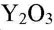
[00150] 제 1 전하 트랩핑 층(1016)을 위한 적합한 두께는 약 30Å 내지 약 80Å일 수 있으며(일부 변화가 허용되며, 예를 들어, ±10 A), 그 중 약 5-20Å은 터널링-방지 층(1020)을 형성하기 위해 라디컬 산화에 의해 소모될 수 있다. 제 2 전하-트랩핑 층(1018)에 대한 적합한 두께는 적어도 30Å일 수 있으며, 그리고 블로킹 유전체(1012)를 위한 적합한 두께는 약 30-70Å일 수 있다.[00150] A suitable thickness for the first
[00151] 도 10a의 메모리 디바이스(1000)는 게이트 제 1 또는 게이트 최종 방식을 이용하여 이루어질 수 있다. 도 11a-f는 도 10a의 비-평면 멀티게이트 디바이스를 제조하기 위한 게이트 제 1 방식을 예시한다. 도 12a-f는 도 10a의 비-평면 멀티게이트 디바이스를 제조하기 위한 게이트 최종 방식을 예시한다.[00151] The
[00152] 도 11a를 참조하면, 게이트 제 1 방식에서 블로킹 산화물과 같은 제 1 또는 하부 유전체 층(1102)이 기판(1106)에서의 소스 또는 드레인과 같은 제 1의, 도핑된 확산 구역(1104) 위에 형성된다. 게이트 층(1108)은 디바이스의 제어 게이트를 형성하기 위해 제 1 유전체 층(1102) 위에 증착되며, 제 2 또는 상부 유전체 층(1110)이 그 위에 형성된다. 상술한 실시예들에 관하여, 제 1 및 제 2 유전체 층들(1102, 1110)이 CVD, 라디컬 산화에 의해 증착될 수 있거나 기판 또는 하부 층의 일부분의 산화에 의해 형성될 수 있다. 게이트 층(1108)은 CVD에 의해 증착되는 금속 증착된 또는 도핑된 폴리실리콘을 포함할 수 있다. 일반적으로 게이트 층(1108)의 두께는 약 40 - 50Å이며, 제 1 및 제 2 유전체 층들(1102, 1110)은 약 20 - 80Å이다.[00152] Referring to FIG. 11A, a first or
[00153] 도 11b를 참조하면, 제 1 개구(1112)는 오버라잉 게이트 층(1108), 및 제 1 및 제 2 유전체 층들(1102, 1110)을 통해 기판(1106)에서의 확산 구역(1104)에 에칭된다. 다음으로, 터널링 산화물(1114), 전하-트랩핑 구역(1116) 및 블로킹 유전체(1118)의 층들이 개구에 순차적으로 증착되며 그리고 상부 유전체 층(1110)의 표면은 도 11c에 도시되는 중간 구조를 산출하기 위해 평탄화한다.[00153] Referring to FIG. 11B, a
[00154] 도시되지 않더라도, 상술한 실시예들에서와 같이 전하-트랩핑 구역(1116)은 터널 산화물(1114)에 더 가까운 적어도 하나의 하부 또는 바닥 전하-트랩핑 층을 포함하는 분리 전하-트랩핑 구역, 및 바닥 전하-트랩핑 층을 오버라잉하는 상부 또는 최상부 전하-트랩핑 층을 포함할 수 있음이 이해될 것이다. 일반적으로, 최상부 전하-트랩핑 층은 실리콘-리치, 산소-린 질화물 층을 포함하며, 그리고 다수의 전하-트랩핑 층들에 분배되는 다수의 전하 트랩들을 포함하는 한편, 바닥 전하-트랩핑 층은 산소-리치 질화물 또는 실리콘 산화질화물을 포함하며, 그 내부의 전하 트랩들의 수를 감소시키기 위해 최상부 전하-트랩핑 층에 대해 산소-리치이다. 일부 실시예들에서, 분리 전하-트랩핑 구역(1116)은 바닥 전하-트랩핑 층으로부터 최상부 전하-트랩핑 층을 분리하는, 산화물과 같은 유전체를 포함하는 적어도 하나의 얇은, 중간 또는 터널링-방지 층을 더 포함한다.[00154] Although not shown, as in the above-described embodiments, the charge-trapping
[00155] 다음으로, 제 2 또는 채널 개구(1120)은 도 11d에서 터널링 산화물(1114), 전하-트랩핑 구역(1116) 및 블로킹 유전체(1118)를 통해 이방성으로 에칭된다. 도 11e를 참조하면, 반도체 재료(1122)가 그 내부에 수직 채널(1124)을 형성하기 위해 채널 개구에 증착된다. 수직 채널(1124)은 반도체 재료의 실질적으로 솔리드 실린더의 외부 층에서의 환형 구역을 포함할 수 있거나, 도 11e에 도시된 바와 같이, 유전체 필러 재료(1126)의 실린더를 둘러싸는 별개의, 층 반도체 재료(1122)를 포함할 수 있다.[00155] Next, the second or
[00156] 도 11f를 참조하면, 상부 유전체 층(1110)의 표면이 평탄화되며 그리고 그 내부에 형성되는, 소스 또는 드레인과 같은 제 2의, 도핑된 확산 구역(1130)을 포함하는 반도체 재료(1128)의 층이 도시된 디바이스를 형성하기 위해 상부 유전체 층 위에 증착된다.[00156] Referring to FIG. 11F, a
[00157] 도 12a를 참조하면, 게이트 최종 방식에서 산화물과 같은 유전체 층(1202)은 기판(1206) 상의 표면 상에 희생 층(1204) 위에 형성되며, 유전체 및 희생 층들을 통해 에칭되는 개구 및 수직 채널(1208)이 그 내부에 형성된다. 상술한 실시예들에 관하여, 수직 채널(1208)은 다결정 또는 단결정 실리콘과 같은 반도체 재료(1210)의 실질적으로 솔리드 실린더의 외부 층에 환형 구역을 포함할 수 있거나, 유전체 필러 재료(도시되지 않음)의 실린더를 둘러싸는 별개의, 층 반도체 재료를 포함할 수 있다. 유전체 층(1202)은 오버라잉 전기적 능동 층 또는 다른 메모리 디바이스로부터 메모리 디바이스(1000)의 후속적으로 형성된 게이트 층을 전기적으로 격리할 수 있는, 실리콘 산화물과 같은 임의의 적합한 유전체 재료를 포함할 수 있다. 희생 층(1204)은 유전체 층(1202), 기판(1206) 및 수직 채널(1208)의 재료에 대해 높은 선택성으로 에칭될 수 있거나 제거될 수 있는 임의의 적합한 재료를 포함할 수 있다.[00157] Referring to FIG. 12A, in the gate final method, a
[00158] 도 12b를 참조하면, 제 2 개구(1212)는 기판(1106)에 대해 유전체 및 희생 층들(1202, 1204)을 통해 에칭되며, 그리고 희생 층(1204)이 에칭되거나 제거된다. 희생 층(1204)은 유전체 층(1202), 기판(1206) 및 수직 채널(1208)의 재료에 대해 높은 선택성으로 에칭될 수 있거나 제거될 수 있는 임의의 적합한 재료를 포함할 수 있다. 일 실시예에서 희생 층(1204)은 버퍼링된 산화물 에칭(Buffered Oxide Etch: BOE 에칭)에 의해 제거될 수 있다.Referring to FIG. 12B, the
[00159] 도 12c 및 12d를 참조하면, 터널링 산화물(1214), 전하-트랩핑 구역(1216) 및 블로킹 유전체(1218)의 층들이 개구에 순차적으로 증착되며 그리고 유전체 층(1202)의 표면은 도 12c에 도시되는 중간 구조를 산출하기 위해 평탄화한다. 도 12d에 도시된 것과 같은 일부 실시예들에서, 전하-트랩핑 구역(1216)은 터널 산화물(1214)에 가장 가까운 적어도 제 1 또는 내부 전하-트랩핑 층(1216a), 및 제 2 또는 외부 전하 트랩핑 층(1216b)을 포함하는 분리 전하-트랩핑 구역일 수 있다. 임의선택적으로, 제 1 및 제 2 전하 트랩핑 층들은 중간 산화물 또는 터널링-방지 층(1220)에 의해 분리될 수 있다.12C and 12D, layers of
[00160] 다음으로, 게이트 층(1222)이 제 2 개구(1212)로 증착되며 도 12e에 예시되는 중간 구조를 산출하기 위해 상부 유전체 층(1212)의 표면이 평탄화된다. 상술한 실시예들에 관하여, 게이트 층(1222)은 금속 증착된 또는 도핑된 폴리실리콘을 포함할 수 있다. 마지막으로, 개구(1224)는 별개의 메모리 디바이스들(1226)의 제어 게이트를 형성하기 위해 게이트 층(1222)을 통해 에칭된다.Next, a
[00161] 이와 같이, 로직 디바이스들로 전하 트랩 메모리 디바이스들을 집적하는 반도체 구조 및 그것을 형성하기 위한 방법이 개시되었다. 본 발명은 구조적 피처들 또는 방법론적 동작들에 특정한 언어도 설명되었더라도, 첨부된 청구범위에 정의되는 본 발명은 반드시 설명된 특정 피처들 또는 동작들로 제한되는 것은 아님이 이해될 것이다. 개시된 특정 피처들 및 동작들은 본 발명을 제한하기보다는 오히려 예시하기 위한 노력으로 청구된 발명의 특히 적절한 구현들로서 이해되는 것이다.As such, a semiconductor structure for integrating charge trap memory devices into logic devices and a method for forming the same has been disclosed. Although the invention has also been described in language specific to structural features or methodological actions, it will be understood that the invention as defined in the appended claims is not necessarily limited to the specific features or actions described. The specific features and acts disclosed are to be understood as particularly suitable implementations of the claimed invention in an effort to illustrate rather than limit the invention.
Claims (20)
기판의 제 1 구역에 상기 기판의 표면을 오버라잉(overlying)하는 반도체 재료로부터 메모리 디바이스의 채널을 형성하는 단계―상기 채널은 상기 메모리 디바이스의 소스 및 드레인을 접속함―;
상기 채널의 복수의 표면들 근처의 상기 채널 위에 전하 트랩핑 유전체 스택을 형성하는 단계―상기 전하 트랩핑 유전체 스택은 터널링 층 위의 전하 트랩핑 층 상에 블로킹 층을 포함함―; 및
상기 전하 트랩핑 층 위에 게이트 층을 형성하는 단계―상기 게이트 층은 큰 일 함수 (high work function) 를 갖는 제 1 게이트 재료로부터 형성됨―,
상기 기판의 제 2 구역 위에 MOS 디바이스를 형성하는 단계―상기 MOS 디바이스를 형성하는 단계는 상기 MOS 디바이스의 게이트 유전체 층 및 상기 블로킹 층을 형성하기 위해 열적 산화를 수행하는 단계를 포함함―; 및
상기 MOS 디바이스 위에 게이트 층을 형성하는 단계―상기 게이트 층은 상기 제 1 게이트 재료와는 상이한 제 2 재료로부터 형성됨―를 포함하는,
방법.As a method,
Forming a channel of a memory device from a semiconductor material overlying a surface of the substrate in a first region of the substrate, the channel connecting a source and a drain of the memory device;
Forming a charge trapping dielectric stack over the channel near the plurality of surfaces of the channel, the charge trapping dielectric stack comprising a blocking layer on the charge trapping layer over the tunneling layer; And
Forming a gate layer over the charge trapping layer, wherein the gate layer is formed from a first gate material having a high work function,
Forming a MOS device over a second region of the substrate, wherein forming the MOS device includes performing thermal oxidation to form a gate dielectric layer and the blocking layer of the MOS device; And
Forming a gate layer over the MOS device, wherein the gate layer is formed from a second material different from the first gate material.
Way.
상기 게이트 유전체 층 및 상기 블로킹 층을 동시에 질화하기 위해 질화 프로세스를 수행하는 단계를 더 포함하는,
방법.The method of claim 1,
Further comprising performing a nitridation process to nitrate the gate dielectric layer and the blocking layer at the same time,
Way.
상기 전하 트랩핑 유전체 스택을 형성하는 단계는:
상기 기판의 상기 제 1 구역을 노출하기 위해 습식 에천트(etchant)로 희생 유전체 층에서의 윈도우(window)를 개방하는 단계;
상기 윈도우에, 상기 터널링 층 위의 상기 전하 트랩핑 층 상에 상기 블로킹 층을 형성하는 단계; 및
상기 희생 유전체 층을 습식 에칭하는 단계
를 더 포함하는,
방법.The method of claim 1,
Forming the charge trapping dielectric stack comprises:
Opening a window in the sacrificial dielectric layer with a wet etchant to expose the first region of the substrate;
In the window, forming the blocking layer on the charge trapping layer over the tunneling layer; And
Wet etching the sacrificial dielectric layer
Further comprising,
Way.
상기 전하 트랩핑 층은 터널 산화물에 더 가까운 질화물을 포함하는 하부 전하-트랩핑 층, 및 상기 하부 전하-트랩핑 층에 대하여 산소-린(lean)인 상부 전하-트랩핑 층을 포함하는 다수의 전하-트랩핑 층들을 포함하며, 그리고 다수의 전하-트랩핑 층들에 분배되는 다수의 전하 트랩들을 포함하는,
방법.The method of claim 1,
The charge trapping layer comprises a lower charge-trapping layer comprising nitride closer to the tunnel oxide, and an upper charge-trapping layer that is oxygen-lean with respect to the lower charge-trapping layer. Comprising charge-trapping layers, and comprising a plurality of charge traps distributed among a plurality of charge-trapping layers,
Way.
상기 기판의 상기 제 2 구역 위에 게이트 유전체 층을 형성하는 단계를 더 포함하며, 상기 게이트 유전체 층은 높은 K 게이트 유전체를 포함하는,
방법.The method of claim 4,
Forming a gate dielectric layer over the second region of the substrate, the gate dielectric layer comprising a high K gate dielectric,
Way.
상기 높은 K 게이트 유전체 위에 금속 게이트 층을 형성하는 단계를 더 포함하는,
방법.The method of claim 5,
Further comprising forming a metal gate layer over the high K gate dielectric,
Way.
상기 전하 트랩핑 층은 상기 상부 전하 트랩핑 층 및 상기 하부 전하 트랩핑 층을 분리하는 중간 산화물 층을 더 포함하며, 상기 게이트 유전체 층은 높은 K 게이트 유전체를 포함하는,
방법.The method of claim 4,
The charge trapping layer further comprises an intermediate oxide layer separating the upper charge trapping layer and the lower charge trapping layer, the gate dielectric layer comprising a high K gate dielectric,
Way.
상기 높은 K 게이트 유전체 위에 금속 게이트 층을 형성하는 단계를 더 포함하는,
방법.The method of claim 7,
Further comprising forming a metal gate layer over the high K gate dielectric,
Way.
상기 채널을 형성하는 단계는 상기 채널의 긴 축에 대하여 <100> 표면 결정 배향을 갖는 실리콘으로 상기 채널을 형성하는 단계를 포함하는,
방법.The method of claim 7,
The step of forming the channel comprises forming the channel from silicon having a <100> surface crystal orientation with respect to the long axis of the channel,
Way.
기판의 제 1 구역 위에 메모리 디바이스를 형성하는 단계 ― 상기 단계는:
상기 기판 위에 적어도 하나의 게이트 층에 의해 분리되는 적어도 2개의 유전체 층들을 포함하는 스택 층을 형성하는 단계;
상기 유전체 층들 및 상기 게이트 층 중 적어도 하나를 통해 상기 스택 층의 최상부 표면으로부터 연장하는 제 1 개구를 형성하는 단계;
상기 제 1 개구의 내부의 측벽 상에 전하 트랩핑 유전체 스택을 형성하는 단계;
전하 트랩핑 층 위에 게이트 층을 형성하는 단계―상기 게이트 층은 큰 일 함수 (high work function) 를 갖는 제 1 게이트 재료로부터 형성됨―; 및
반도체 재료를 상기 제 1 개구의 내부의 전하 트랩핑 유전체 스택 위에 증착하는 단계를 포함하는 상기 메모리 디바이스의 채널을 형성하는 단계를 포함함 ―; 및
상기 유전체 층들 및 상기 게이트 층 중 적어도 하나를 통해 상기 스택 층의 최상부 표면으로부터 연장하는 제 2 개구를 형성하는 단계를 포함하는 상기 기판의 제 2 구역 위에 MOS 디바이스를 형성하는 단계를 포함하고,
상기 전하 트랩핑 유전체 스택을 형성하는 단계는 상기 제 1 개구의 내부의 상기 측벽 상에 블로킹 층을 형성하는 단계, 상기 블로킹 층 위에 상기 전하 트랩핑 층을 형성하는 단계, 및 상기 전하 트랩핑 유전체 층 위에 터널링 층을 형성하는 단계를 포함하고,
상기 MOS 디바이스를 형성하는 단계는 상기 MOS 디바이스의 게이트 유전체 층 및 상기 블로킹 층을 동시에 형성하기 위해 열적 산화를 수행하는 단계를 포함하며,
상기 MOS 디바이스 위에 게이트 층을 형성하는 단계―상기 게이트 층은 상기 제 1 게이트 재료와는 상이한 제 2 재료로부터 형성됨―를 더 포함하는,
방법.As a method,
Forming a memory device over the first region of the substrate, the step comprising:
Forming a stack layer comprising at least two dielectric layers separated by at least one gate layer over the substrate;
Forming a first opening extending from a top surface of the stack layer through at least one of the dielectric layers and the gate layer;
Forming a charge trapping dielectric stack on the inner sidewall of the first opening;
Forming a gate layer over the charge trapping layer, the gate layer formed from a first gate material having a high work function; And
Forming a channel of the memory device comprising depositing a semiconductor material over a charge trapping dielectric stack in the interior of the first opening; And
Forming a MOS device over a second region of the substrate comprising forming a second opening extending from a top surface of the stack layer through at least one of the dielectric layers and the gate layer,
The forming of the charge trapping dielectric stack may include forming a blocking layer on the sidewall inside the first opening, forming the charge trapping layer over the blocking layer, and the charge trapping dielectric layer. Forming a tunneling layer thereon,
Forming the MOS device comprises performing thermal oxidation to simultaneously form the gate dielectric layer and the blocking layer of the MOS device,
Forming a gate layer over the MOS device, wherein the gate layer is formed from a second material different from the first gate material.
Way.
상기 게이트 유전체 층 및 상기 블로킹 층을 동시에 질화하기 위해 질화 프로세스를 수행하는 단계를 더 포함하는,
방법.The method of claim 10,
Further comprising performing a nitridation process to nitrate the gate dielectric layer and the blocking layer at the same time,
Way.
상기 전하 트랩핑 층은 질화물을 포함하는 제 1 서브-층, 및 상기 제 1 서브-층에 대해 산소-린인 제 2 서브-층을 포함하는 다수의 전하-트랩핑 층들을 포함하고, 다수의 전하-트랩핑 층들에서 분배되는 다수의 전하 트랩들을 포함하며, 상기 제 1 서브-층이 상기 터널링 층에 더 가까운,
방법.The method of claim 10,
The charge trapping layer comprises a plurality of charge-trapping layers including a first sub-layer comprising nitride, and a second sub-layer that is oxygen-line relative to the first sub-layer, and a plurality of charge -Contains a plurality of charge traps distributed in the trapping layers, the first sub-layer closer to the tunneling layer,
Way.
질화 프로세스는 복수의 질소 어닐링들을 포함하는,
방법.The method of claim 12,
The nitridation process comprises a plurality of nitrogen annealings,
Way.
상기 전하 트랩핑 층은 상기 상부 전하-트랩핑 층 및 상기 하부 전하-트랩핑 층을 분리하는 중간 산화물 층을 더 포함하며, 상기 게이트 유전체 층은 높은 K 게이트 유전체를 포함하는,
방법.The method of claim 12,
The charge trapping layer further comprises an intermediate oxide layer separating the upper charge-trapping layer and the lower charge-trapping layer, the gate dielectric layer comprising a high K gate dielectric,
Way.
상기 게이트 층은 금속을 포함하는,
방법.The method of claim 14,
The gate layer comprises a metal,
Way.
기판의 제 1 구역 위에 메모리 디바이스를 형성하는 단계 ― 상기 단계는:
상기 기판 위에 희생 층을 오버라잉하는 적어도 하나의 유전체 층을 포함하는 스택 층을 형성하는 단계,
상기 유전체 층 및 상기 희생 층을 통해 상기 스택 층의 최상부 표면으로부터 연장하는 제 1 개구를 형성하는 단계,
상기 제 1 개구에 상기 메모리 디바이스의 채널을 형성하는 단계,
상기 유전체 층을 통해 상기 최상부 표면으로부터 연장하는 제 2 개구를 형성하는 단계 및 상기 채널의 적어도 일부분을 노출하기 위해 상기 채널 근처에 상기 희생 층의 적어도 일부분을 제거하는 단계,
상기 채널의 상기 노출된 부분 상에 전하 트랩핑 유전체 스택을 형성하는 단계, 및
상기 전하 트랩핑 유전체 스택 상에 게이트 층을 형성하는 단계―상기 게이트 층은 큰 일 함수 (high work function) 를 갖는 제 1 게이트 재료로부터 형성됨―
를 포함함 ―; 및
상기 기판의 제 2 구역 위에 MOS 디바이스를 형성하는 단계
를 포함하고,
상기 전하 트랩핑 유전체 스택을 형성하는 단계는 상기 채널의 상기 노출된 부분 상에 블로킹 층을 형성하는 단계, 상기 블로킹 층 위에 전하 트랩핑 층을 형성하는 단계, 및 상기 전하 트랩핑 유전체 층 위에 터널링 층을 형성하는 단계를 포함하며,
상기 MOS 디바이스를 형성하는 단계는 상기 MOS 디바이스의 게이트 유전체 층 및 상기 블로킹 층을 동시에 형성하기 위해 열적 산화를 수행하는 단계를 포함하고,
상기 MOS 디바이스 위에 게이트 층을 형성하는 단계―상기 게이트 층은 상기 제 1 게이트 재료와는 상이한 제 2 재료로부터 형성됨―를 더 포함하는,
방법.
As a method,
Forming a memory device over the first region of the substrate, the step comprising:
Forming a stack layer comprising at least one dielectric layer overlying a sacrificial layer over the substrate,
Forming a first opening extending from the top surface of the stack layer through the dielectric layer and the sacrificial layer,
Forming a channel of the memory device in the first opening,
Forming a second opening extending from the top surface through the dielectric layer and removing at least a portion of the sacrificial layer near the channel to expose at least a portion of the channel,
Forming a charge trapping dielectric stack on the exposed portion of the channel, and
Forming a gate layer on the charge trapping dielectric stack, wherein the gate layer is formed from a first gate material having a high work function.
Including -; And
Forming a MOS device over the second region of the substrate
Including,
The forming of the charge trapping dielectric stack includes forming a blocking layer on the exposed portion of the channel, forming a charge trapping layer over the blocking layer, and a tunneling layer over the charge trapping dielectric layer. Including the step of forming,
Forming the MOS device comprises performing thermal oxidation to simultaneously form the gate dielectric layer and the blocking layer of the MOS device,
Forming a gate layer over the MOS device, wherein the gate layer is formed from a second material different from the first gate material.
Way.
Applications Claiming Priority (4)
| Application Number | Priority Date | Filing Date | Title |
|---|---|---|---|
| US13/436,878 | 2012-03-31 | ||
| US13/436,878 US8871595B2 (en) | 2007-05-25 | 2012-03-31 | Integration of non-volatile charge trap memory devices and logic CMOS devices |
| KR1020147025063A KR102072181B1 (en) | 2012-03-31 | 2013-03-18 | Integration of non-volatile charge trap memory devices and logic cmos devices |
| PCT/US2013/032777 WO2013148393A1 (en) | 2012-03-31 | 2013-03-18 | Integration of non-volatile charge trap memory devices and logic cmos devices |
Related Parent Applications (1)
| Application Number | Title | Priority Date | Filing Date |
|---|---|---|---|
| KR1020147025063A Division KR102072181B1 (en) | 2012-03-31 | 2013-03-18 | Integration of non-volatile charge trap memory devices and logic cmos devices |
Publications (2)
| Publication Number | Publication Date |
|---|---|
| KR20200012038A KR20200012038A (en) | 2020-02-04 |
| KR102256421B1 true KR102256421B1 (en) | 2021-05-26 |
Family
ID=49261111
Family Applications (2)
| Application Number | Title | Priority Date | Filing Date |
|---|---|---|---|
| KR1020207002501A Active KR102256421B1 (en) | 2012-03-31 | 2013-03-18 | Integration of non-volatile charge trap memory devices and logic cmos devices |
| KR1020147025063A Active KR102072181B1 (en) | 2012-03-31 | 2013-03-18 | Integration of non-volatile charge trap memory devices and logic cmos devices |
Family Applications After (1)
| Application Number | Title | Priority Date | Filing Date |
|---|---|---|---|
| KR1020147025063A Active KR102072181B1 (en) | 2012-03-31 | 2013-03-18 | Integration of non-volatile charge trap memory devices and logic cmos devices |
Country Status (6)
| Country | Link |
|---|---|
| EP (2) | EP2831919A4 (en) |
| JP (1) | JP6465791B2 (en) |
| KR (2) | KR102256421B1 (en) |
| CN (1) | CN104350603B (en) |
| TW (1) | TWI582854B (en) |
| WO (1) | WO2013148393A1 (en) |
Families Citing this family (17)
| Publication number | Priority date | Publication date | Assignee | Title |
|---|---|---|---|---|
| US9218978B1 (en) * | 2015-03-09 | 2015-12-22 | Cypress Semiconductor Corporation | Method of ONO stack formation |
| KR102394938B1 (en) * | 2015-05-21 | 2022-05-09 | 삼성전자주식회사 | Semiconductor devices and methods of manufacturing semiconductor devices |
| JP2017050537A (en) * | 2015-08-31 | 2017-03-09 | 株式会社半導体エネルギー研究所 | Semiconductor device |
| CN106887409B (en) * | 2015-12-15 | 2020-02-21 | 上海新昇半导体科技有限公司 | Complementary nanowire semiconductor device and method of making the same |
| US9704995B1 (en) * | 2016-09-20 | 2017-07-11 | Advanced Micro Devices, Inc. | Gate all around device architecture with local oxide |
| JP2017028307A (en) * | 2016-10-05 | 2017-02-02 | ルネサスエレクトロニクス株式会社 | Semiconductor device manufacturing method |
| US10468530B2 (en) | 2017-11-15 | 2019-11-05 | Taiwan Semiconductor Manufacturing Co., Ltd. | Semiconductor structure with source/drain multi-layer structure and method for forming the same |
| US10699960B2 (en) * | 2018-06-27 | 2020-06-30 | Taiwan Semiconductor Manufacturing Co., Ltd. | Methods for improving interlayer dielectric layer topography |
| CN109473341A (en) * | 2018-11-16 | 2019-03-15 | 扬州扬杰电子科技股份有限公司 | A kind of processing technology of small-angle oxide layer steps |
| GB2591472B (en) | 2020-01-28 | 2022-02-09 | X Fab France Sas | Method of forming asymmetric differential spacers for optimized MOSFET performance and optimized mosfet and SONOS co-integration |
| CN112233974A (en) * | 2020-10-26 | 2021-01-15 | 广州粤芯半导体技术有限公司 | Method for preventing side erosion in wet etching and method for forming trench gate |
| KR102795036B1 (en) * | 2020-11-02 | 2025-04-11 | 삼성디스플레이 주식회사 | Display device |
| CN112635487B (en) * | 2020-12-17 | 2024-06-04 | 长江存储科技有限责任公司 | Semiconductor device, method for manufacturing semiconductor device, mask plate system |
| KR102876628B1 (en) | 2021-01-15 | 2025-10-28 | 에스케이하이닉스 주식회사 | 3D Semiconductor Device Including a Word line Structure Having a Protruding Portion |
| US11848339B2 (en) * | 2021-03-19 | 2023-12-19 | Taiwan Semiconductor Manufacturing Company Ltd. | Semiconductor structure including isolation structure and method for forming isolation structure |
| US20230050475A1 (en) * | 2021-08-13 | 2023-02-16 | The Hong Kong University Of Science And Technology | Wide-Bandgap Semiconductor Bipolar Charge-Trapping Non-Volatile Memory with Single Insulating Layer and A Fabrication Method Thereof |
| CN116266607A (en) * | 2021-12-16 | 2023-06-20 | 成都高真科技有限公司 | Transistor stress relief method for memory device |
Family Cites Families (23)
| Publication number | Priority date | Publication date | Assignee | Title |
|---|---|---|---|---|
| KR100881201B1 (en) * | 2003-01-09 | 2009-02-05 | 삼성전자주식회사 | Sonos memory device having a side gate and its manufacturing method |
| JP4242822B2 (en) * | 2004-10-22 | 2009-03-25 | パナソニック株式会社 | Manufacturing method of semiconductor device |
| US7298004B2 (en) * | 2004-11-30 | 2007-11-20 | Infineon Technologies Ag | Charge-trapping memory cell and method for production |
| US7473589B2 (en) * | 2005-12-09 | 2009-01-06 | Macronix International Co., Ltd. | Stacked thin film transistor, non-volatile memory devices and methods for fabricating the same |
| JP2006294756A (en) * | 2005-04-07 | 2006-10-26 | Canon Inc | Manufacturing method of semiconductor device |
| US7514323B2 (en) * | 2005-11-28 | 2009-04-07 | International Business Machines Corporation | Vertical SOI trench SONOS cell |
| US8772858B2 (en) * | 2006-10-11 | 2014-07-08 | Macronix International Co., Ltd. | Vertical channel memory and manufacturing method thereof and operating method using the same |
| US7811890B2 (en) * | 2006-10-11 | 2010-10-12 | Macronix International Co., Ltd. | Vertical channel transistor structure and manufacturing method thereof |
| JP5118347B2 (en) * | 2007-01-05 | 2013-01-16 | 株式会社東芝 | Semiconductor device |
| US8063434B1 (en) * | 2007-05-25 | 2011-11-22 | Cypress Semiconductor Corporation | Memory transistor with multiple charge storing layers and a high work function gate electrode |
| US8093128B2 (en) * | 2007-05-25 | 2012-01-10 | Cypress Semiconductor Corporation | Integration of non-volatile charge trap memory devices and logic CMOS devices |
| US8283261B2 (en) * | 2007-05-25 | 2012-10-09 | Cypress Semiconductor Corporation | Radical oxidation process for fabricating a nonvolatile charge trap memory device |
| US8643124B2 (en) * | 2007-05-25 | 2014-02-04 | Cypress Semiconductor Corporation | Oxide-nitride-oxide stack having multiple oxynitride layers |
| JP2009027134A (en) * | 2007-06-21 | 2009-02-05 | Tokyo Electron Ltd | MOS type semiconductor memory device |
| TW200913162A (en) * | 2007-09-11 | 2009-03-16 | Univ Nat Chiao Tung | Nonvolatile memory device with nanowire channel and a method for fabricating the same |
| KR101226685B1 (en) * | 2007-11-08 | 2013-01-25 | 삼성전자주식회사 | Vertical type semiconductor device and Method of manufacturing the same |
| US20110012090A1 (en) * | 2007-12-07 | 2011-01-20 | Agency For Science, Technology And Research | Silicon-germanium nanowire structure and a method of forming the same |
| KR100937669B1 (en) * | 2007-12-28 | 2010-01-19 | 주식회사 동부하이텍 | Quantum Trap Nonvolatile Memory Devices |
| KR20100111163A (en) * | 2009-04-06 | 2010-10-14 | 삼성전자주식회사 | Nonvolatile memory device |
| US8071453B1 (en) * | 2009-04-24 | 2011-12-06 | Cypress Semiconductor Corporation | Method of ONO integration into MOS flow |
| JP2011023464A (en) * | 2009-07-14 | 2011-02-03 | Toshiba Corp | Semiconductor memory device |
| US8138543B2 (en) * | 2009-11-18 | 2012-03-20 | International Business Machines Corporation | Hybrid FinFET/planar SOI FETs |
| JP5457815B2 (en) * | 2009-12-17 | 2014-04-02 | 株式会社東芝 | Nonvolatile semiconductor memory device |
-
2013
- 2013-03-18 KR KR1020207002501A patent/KR102256421B1/en active Active
- 2013-03-18 EP EP13769241.4A patent/EP2831919A4/en not_active Withdrawn
- 2013-03-18 CN CN201380016420.2A patent/CN104350603B/en active Active
- 2013-03-18 KR KR1020147025063A patent/KR102072181B1/en active Active
- 2013-03-18 EP EP16188153.7A patent/EP3229276A1/en active Pending
- 2013-03-18 WO PCT/US2013/032777 patent/WO2013148393A1/en not_active Ceased
- 2013-03-18 JP JP2015503361A patent/JP6465791B2/en active Active
- 2013-03-21 TW TW102110015A patent/TWI582854B/en active
Also Published As
| Publication number | Publication date |
|---|---|
| JP6465791B2 (en) | 2019-02-06 |
| TW201347048A (en) | 2013-11-16 |
| JP2015516679A (en) | 2015-06-11 |
| EP2831919A4 (en) | 2016-03-23 |
| TWI582854B (en) | 2017-05-11 |
| CN104350603B (en) | 2017-09-15 |
| KR102072181B1 (en) | 2020-03-02 |
| EP3229276A1 (en) | 2017-10-11 |
| KR20150011792A (en) | 2015-02-02 |
| WO2013148393A1 (en) | 2013-10-03 |
| KR20200012038A (en) | 2020-02-04 |
| EP2831919A1 (en) | 2015-02-04 |
| CN104350603A (en) | 2015-02-11 |
Similar Documents
| Publication | Publication Date | Title |
|---|---|---|
| KR102256421B1 (en) | Integration of non-volatile charge trap memory devices and logic cmos devices | |
| US8871595B2 (en) | Integration of non-volatile charge trap memory devices and logic CMOS devices | |
| US8093128B2 (en) | Integration of non-volatile charge trap memory devices and logic CMOS devices | |
| US10424592B2 (en) | Method of integrating a charge-trapping gate stack into a CMOS flow | |
| JP6562518B2 (en) | Integration of memory transistors into high-k, metal gate CMOS process flow | |
| US9911613B2 (en) | Method of fabricating a charge-trapping gate stack using a CMOS process flow | |
| US9893172B2 (en) | Methods to integrate SONOS into CMOS flow | |
| CN104769724B (en) | Memory transistor with multiple charge storage layers |
Legal Events
| Date | Code | Title | Description |
|---|---|---|---|
| A107 | Divisional application of patent | ||
| PA0104 | Divisional application for international application |
Comment text: Divisional Application for International Patent Patent event code: PA01041R01D Patent event date: 20200123 Application number text: 1020147025063 Filing date: 20140905 |
|
| PG1501 | Laying open of application | ||
| A201 | Request for examination | ||
| PA0201 | Request for examination |
Patent event code: PA02012R01D Patent event date: 20200221 Comment text: Request for Examination of Application |
|
| E902 | Notification of reason for refusal | ||
| PE0902 | Notice of grounds for rejection |
Comment text: Notification of reason for refusal Patent event date: 20200330 Patent event code: PE09021S01D |
|
| E90F | Notification of reason for final refusal | ||
| PE0902 | Notice of grounds for rejection |
Comment text: Final Notice of Reason for Refusal Patent event date: 20200819 Patent event code: PE09021S02D |
|
| E701 | Decision to grant or registration of patent right | ||
| PE0701 | Decision of registration |
Patent event code: PE07011S01D Comment text: Decision to Grant Registration Patent event date: 20210223 |
|
| GRNT | Written decision to grant | ||
| PR0701 | Registration of establishment |
Comment text: Registration of Establishment Patent event date: 20210520 Patent event code: PR07011E01D |
|
| PR1002 | Payment of registration fee |
Payment date: 20210520 End annual number: 3 Start annual number: 1 |
|
| PG1601 | Publication of registration | ||
| PR1001 | Payment of annual fee |
Payment date: 20240513 Start annual number: 4 End annual number: 4 |