KR102192001B1 - Carbazole compound and organic light emitting diode including the same - Google Patents
Carbazole compound and organic light emitting diode including the same Download PDFInfo
- Publication number
- KR102192001B1 KR102192001B1 KR1020140038217A KR20140038217A KR102192001B1 KR 102192001 B1 KR102192001 B1 KR 102192001B1 KR 1020140038217 A KR1020140038217 A KR 1020140038217A KR 20140038217 A KR20140038217 A KR 20140038217A KR 102192001 B1 KR102192001 B1 KR 102192001B1
- Authority
- KR
- South Korea
- Prior art keywords
- light emitting
- charge generation
- layer
- generation layer
- organic light
- Prior art date
- Legal status (The legal status is an assumption and is not a legal conclusion. Google has not performed a legal analysis and makes no representation as to the accuracy of the status listed.)
- Active
Links
- FANIJKVUZCLTDM-UHFFFAOYSA-N c(cc1)ccc1-[n]1c(nccc2)c2c2c1ccc(-c1cnc3c(nccc4)c4ccc3c1)c2 Chemical compound c(cc1)ccc1-[n]1c(nccc2)c2c2c1ccc(-c1cnc3c(nccc4)c4ccc3c1)c2 FANIJKVUZCLTDM-UHFFFAOYSA-N 0.000 description 1
- QQMCPUJPNFVUAJ-UHFFFAOYSA-N c(cc1)ccc1-[n]1c(nccc2)c2c2cc(-c(cc3c4cccnc44)ccc3[n]4-c3ccccc3)ccc12 Chemical compound c(cc1)ccc1-[n]1c(nccc2)c2c2cc(-c(cc3c4cccnc44)ccc3[n]4-c3ccccc3)ccc12 QQMCPUJPNFVUAJ-UHFFFAOYSA-N 0.000 description 1
- BPVXWKNDPCOVPF-UHFFFAOYSA-N c(cc1)ccc1-[n]1c(nccc2)c2c2cc(-c3cccc(-c4nc(-c5ncccc5)nc(-c5ncccc5)n4)c3)ccc12 Chemical compound c(cc1)ccc1-[n]1c(nccc2)c2c2cc(-c3cccc(-c4nc(-c5ncccc5)nc(-c5ncccc5)n4)c3)ccc12 BPVXWKNDPCOVPF-UHFFFAOYSA-N 0.000 description 1
- XHANNISLRWOMRC-UHFFFAOYSA-N c(cc1)ccc1-[n]1c2ncccc2c2c1ccc(-c(cc1)ccc1-c1nc(-c3ncccc3)nc(-c3ncccc3)n1)c2 Chemical compound c(cc1)ccc1-[n]1c2ncccc2c2c1ccc(-c(cc1)ccc1-c1nc(-c3ncccc3)nc(-c3ncccc3)n1)c2 XHANNISLRWOMRC-UHFFFAOYSA-N 0.000 description 1
- PKZGVFZUTIMAFT-UHFFFAOYSA-N c(cc1)ccc1-[n]1c2ncccc2c2c1ccc(-c(cc1)ccc1-c1ncccc1)c2 Chemical compound c(cc1)ccc1-[n]1c2ncccc2c2c1ccc(-c(cc1)ccc1-c1ncccc1)c2 PKZGVFZUTIMAFT-UHFFFAOYSA-N 0.000 description 1
- YXFAYAMONYCWTA-UHFFFAOYSA-N c(cc1)ccc1-[n]1c2ncccc2c2c1ccc(-c(cc1)ccc1N(c1ncccc1)c1ncccc1)c2 Chemical compound c(cc1)ccc1-[n]1c2ncccc2c2c1ccc(-c(cc1)ccc1N(c1ncccc1)c1ncccc1)c2 YXFAYAMONYCWTA-UHFFFAOYSA-N 0.000 description 1
- NTVXXAXBXRKXLF-UHFFFAOYSA-N c(cc1)ccc1-[n]1c2ncccc2c2c1ccc(-c(nc1)ccc1-c1ccccn1)c2 Chemical compound c(cc1)ccc1-[n]1c2ncccc2c2c1ccc(-c(nc1)ccc1-c1ccccn1)c2 NTVXXAXBXRKXLF-UHFFFAOYSA-N 0.000 description 1
- VLYIKUIAJYZEAQ-UHFFFAOYSA-N c(cc1)ccc1-[n]1c2ncccc2c2c1ccc(-c1c(cccc3)c3ccc1)c2 Chemical compound c(cc1)ccc1-[n]1c2ncccc2c2c1ccc(-c1c(cccc3)c3ccc1)c2 VLYIKUIAJYZEAQ-UHFFFAOYSA-N 0.000 description 1
- OVKWCOGHKHEPKL-UHFFFAOYSA-N c(cc1)ccc1-[n]1c2ncccc2c2c1ccc(-c1ccc(cccc3)c3n1)c2 Chemical compound c(cc1)ccc1-[n]1c2ncccc2c2c1ccc(-c1ccc(cccc3)c3n1)c2 OVKWCOGHKHEPKL-UHFFFAOYSA-N 0.000 description 1
- MYYPFXHIRLMARW-UHFFFAOYSA-N c(cc1)ccc1-[n]1c2ncccc2c2c1ccc(-c1nc(c(nccc3)c3cc3)c3cc1)c2 Chemical compound c(cc1)ccc1-[n]1c2ncccc2c2c1ccc(-c1nc(c(nccc3)c3cc3)c3cc1)c2 MYYPFXHIRLMARW-UHFFFAOYSA-N 0.000 description 1
- FCCYYPSFSGRFJG-UHFFFAOYSA-N c(cc1)ccc1-[n]1c2ncccc2c2c1ccc(-c1nccc3c1cccc3)c2 Chemical compound c(cc1)ccc1-[n]1c2ncccc2c2c1ccc(-c1nccc3c1cccc3)c2 FCCYYPSFSGRFJG-UHFFFAOYSA-N 0.000 description 1
- VIKSYJFMWWLYNU-UHFFFAOYSA-N c(cc1)ccc1-c(cc1)ccc1-c(cc1)cc(c2cccnc22)c1[n]2-c1ccccc1 Chemical compound c(cc1)ccc1-c(cc1)ccc1-c(cc1)cc(c2cccnc22)c1[n]2-c1ccccc1 VIKSYJFMWWLYNU-UHFFFAOYSA-N 0.000 description 1
- FPTMVECVRDYBBE-UHFFFAOYSA-N c(cc1)ccc1N(c(cc1)ccc1-c(cc1)cc(c2cccnc22)c1[n]2-c1ccccc1)c1ccc(ccc2c3nccc2)c3n1 Chemical compound c(cc1)ccc1N(c(cc1)ccc1-c(cc1)cc(c2cccnc22)c1[n]2-c1ccccc1)c1ccc(ccc2c3nccc2)c3n1 FPTMVECVRDYBBE-UHFFFAOYSA-N 0.000 description 1
- QMZOMKWAACHUQL-UHFFFAOYSA-N c(cc1)ccc1N(c(cc1)ccc1-c(cc1)cc(c2cccnc22)c1[n]2-c1ccccn1)c1nc(c(nccc2)c2cc2)c2cc1 Chemical compound c(cc1)ccc1N(c(cc1)ccc1-c(cc1)cc(c2cccnc22)c1[n]2-c1ccccn1)c1nc(c(nccc2)c2cc2)c2cc1 QMZOMKWAACHUQL-UHFFFAOYSA-N 0.000 description 1
- CDKVWUGVTSOZPT-UHFFFAOYSA-N c(cc1)ccc1N(c1ccccc1)c(cc1)ccc1-c(cc1)cc(c2cccnc22)c1[n]2-c1ncccc1 Chemical compound c(cc1)ccc1N(c1ccccc1)c(cc1)ccc1-c(cc1)cc(c2cccnc22)c1[n]2-c1ncccc1 CDKVWUGVTSOZPT-UHFFFAOYSA-N 0.000 description 1
- MCXYABHLNLOFHZ-UHFFFAOYSA-N c1cc(-c2nc(-c(cc3)cc(c4c5nccc4)c3[n]5-c3ccccn3)nc(-c3ncccc3)n2)ncc1 Chemical compound c1cc(-c2nc(-c(cc3)cc(c4c5nccc4)c3[n]5-c3ccccn3)nc(-c3ncccc3)n2)ncc1 MCXYABHLNLOFHZ-UHFFFAOYSA-N 0.000 description 1
- QUNYIEJLJNSZQN-UHFFFAOYSA-N c1cc(N(c(cc2)ccc2-c(cc2)cc(c3cccnc33)c2[n]3-c2ncccc2)c2ncccc2)ncc1 Chemical compound c1cc(N(c(cc2)ccc2-c(cc2)cc(c3cccnc33)c2[n]3-c2ncccc2)c2ncccc2)ncc1 QUNYIEJLJNSZQN-UHFFFAOYSA-N 0.000 description 1
- DTTLSFZMGXMCIC-UHFFFAOYSA-N c1ccnc(N(c(cc2)ccc2-c(cc2)cc(c3cccnc33)c2[n]3-c2ccccn2)c2nc3c4ncccc4ccc3cc2)c1 Chemical compound c1ccnc(N(c(cc2)ccc2-c(cc2)cc(c3cccnc33)c2[n]3-c2ccccn2)c2nc3c4ncccc4ccc3cc2)c1 DTTLSFZMGXMCIC-UHFFFAOYSA-N 0.000 description 1
Images


Classifications
-
- C—CHEMISTRY; METALLURGY
- C07—ORGANIC CHEMISTRY
- C07D—HETEROCYCLIC COMPOUNDS
- C07D471/00—Heterocyclic compounds containing nitrogen atoms as the only ring hetero atoms in the condensed system, at least one ring being a six-membered ring with one nitrogen atom, not provided for by groups C07D451/00 - C07D463/00
- C07D471/02—Heterocyclic compounds containing nitrogen atoms as the only ring hetero atoms in the condensed system, at least one ring being a six-membered ring with one nitrogen atom, not provided for by groups C07D451/00 - C07D463/00 in which the condensed system contains two hetero rings
- C07D471/04—Ortho-condensed systems
-
- C—CHEMISTRY; METALLURGY
- C07—ORGANIC CHEMISTRY
- C07D—HETEROCYCLIC COMPOUNDS
- C07D209/00—Heterocyclic compounds containing five-membered rings, condensed with other rings, with one nitrogen atom as the only ring hetero atom
- C07D209/56—Ring systems containing three or more rings
- C07D209/80—[b, c]- or [b, d]-condensed
- C07D209/82—Carbazoles; Hydrogenated carbazoles
-
- C—CHEMISTRY; METALLURGY
- C07—ORGANIC CHEMISTRY
- C07D—HETEROCYCLIC COMPOUNDS
- C07D487/00—Heterocyclic compounds containing nitrogen atoms as the only ring hetero atoms in the condensed system, not provided for by groups C07D451/00 - C07D477/00
- C07D487/02—Heterocyclic compounds containing nitrogen atoms as the only ring hetero atoms in the condensed system, not provided for by groups C07D451/00 - C07D477/00 in which the condensed system contains two hetero rings
- C07D487/04—Ortho-condensed systems
-
- C—CHEMISTRY; METALLURGY
- C09—DYES; PAINTS; POLISHES; NATURAL RESINS; ADHESIVES; COMPOSITIONS NOT OTHERWISE PROVIDED FOR; APPLICATIONS OF MATERIALS NOT OTHERWISE PROVIDED FOR
- C09K—MATERIALS FOR MISCELLANEOUS APPLICATIONS, NOT PROVIDED FOR ELSEWHERE
- C09K11/00—Luminescent materials, e.g. electroluminescent or chemiluminescent
- C09K11/02—Use of particular materials as binders, particle coatings or suspension media therefor
- C09K11/025—Use of particular materials as binders, particle coatings or suspension media therefor non-luminescent particle coatings or suspension media
-
- C—CHEMISTRY; METALLURGY
- C09—DYES; PAINTS; POLISHES; NATURAL RESINS; ADHESIVES; COMPOSITIONS NOT OTHERWISE PROVIDED FOR; APPLICATIONS OF MATERIALS NOT OTHERWISE PROVIDED FOR
- C09K—MATERIALS FOR MISCELLANEOUS APPLICATIONS, NOT PROVIDED FOR ELSEWHERE
- C09K11/00—Luminescent materials, e.g. electroluminescent or chemiluminescent
- C09K11/06—Luminescent materials, e.g. electroluminescent or chemiluminescent containing organic luminescent materials
-
- H—ELECTRICITY
- H10—SEMICONDUCTOR DEVICES; ELECTRIC SOLID-STATE DEVICES NOT OTHERWISE PROVIDED FOR
- H10K—ORGANIC ELECTRIC SOLID-STATE DEVICES
- H10K50/00—Organic light-emitting devices
-
- H—ELECTRICITY
- H10—SEMICONDUCTOR DEVICES; ELECTRIC SOLID-STATE DEVICES NOT OTHERWISE PROVIDED FOR
- H10K—ORGANIC ELECTRIC SOLID-STATE DEVICES
- H10K50/00—Organic light-emitting devices
- H10K50/10—OLEDs or polymer light-emitting diodes [PLED]
- H10K50/11—OLEDs or polymer light-emitting diodes [PLED] characterised by the electroluminescent [EL] layers
- H10K50/125—OLEDs or polymer light-emitting diodes [PLED] characterised by the electroluminescent [EL] layers specially adapted for multicolour light emission, e.g. for emitting white light
- H10K50/13—OLEDs or polymer light-emitting diodes [PLED] characterised by the electroluminescent [EL] layers specially adapted for multicolour light emission, e.g. for emitting white light comprising stacked EL layers within one EL unit
- H10K50/131—OLEDs or polymer light-emitting diodes [PLED] characterised by the electroluminescent [EL] layers specially adapted for multicolour light emission, e.g. for emitting white light comprising stacked EL layers within one EL unit with spacer layers between the electroluminescent layers
-
- H—ELECTRICITY
- H10—SEMICONDUCTOR DEVICES; ELECTRIC SOLID-STATE DEVICES NOT OTHERWISE PROVIDED FOR
- H10K—ORGANIC ELECTRIC SOLID-STATE DEVICES
- H10K85/00—Organic materials used in the body or electrodes of devices covered by this subclass
- H10K85/60—Organic compounds having low molecular weight
- H10K85/615—Polycyclic condensed aromatic hydrocarbons, e.g. anthracene
- H10K85/624—Polycyclic condensed aromatic hydrocarbons, e.g. anthracene containing six or more rings
-
- H—ELECTRICITY
- H10—SEMICONDUCTOR DEVICES; ELECTRIC SOLID-STATE DEVICES NOT OTHERWISE PROVIDED FOR
- H10K—ORGANIC ELECTRIC SOLID-STATE DEVICES
- H10K85/00—Organic materials used in the body or electrodes of devices covered by this subclass
- H10K85/60—Organic compounds having low molecular weight
- H10K85/615—Polycyclic condensed aromatic hydrocarbons, e.g. anthracene
- H10K85/626—Polycyclic condensed aromatic hydrocarbons, e.g. anthracene containing more than one polycyclic condensed aromatic rings, e.g. bis-anthracene
-
- H—ELECTRICITY
- H10—SEMICONDUCTOR DEVICES; ELECTRIC SOLID-STATE DEVICES NOT OTHERWISE PROVIDED FOR
- H10K—ORGANIC ELECTRIC SOLID-STATE DEVICES
- H10K85/00—Organic materials used in the body or electrodes of devices covered by this subclass
- H10K85/60—Organic compounds having low molecular weight
- H10K85/649—Aromatic compounds comprising a hetero atom
- H10K85/654—Aromatic compounds comprising a hetero atom comprising only nitrogen as heteroatom
-
- H—ELECTRICITY
- H10—SEMICONDUCTOR DEVICES; ELECTRIC SOLID-STATE DEVICES NOT OTHERWISE PROVIDED FOR
- H10K—ORGANIC ELECTRIC SOLID-STATE DEVICES
- H10K85/00—Organic materials used in the body or electrodes of devices covered by this subclass
- H10K85/60—Organic compounds having low molecular weight
- H10K85/649—Aromatic compounds comprising a hetero atom
- H10K85/657—Polycyclic condensed heteroaromatic hydrocarbons
- H10K85/6572—Polycyclic condensed heteroaromatic hydrocarbons comprising only nitrogen in the heteroaromatic polycondensed ring system, e.g. phenanthroline or carbazole
-
- H—ELECTRICITY
- H10—SEMICONDUCTOR DEVICES; ELECTRIC SOLID-STATE DEVICES NOT OTHERWISE PROVIDED FOR
- H10K—ORGANIC ELECTRIC SOLID-STATE DEVICES
- H10K50/00—Organic light-emitting devices
- H10K50/10—OLEDs or polymer light-emitting diodes [PLED]
- H10K50/14—Carrier transporting layers
- H10K50/16—Electron transporting layers
-
- H—ELECTRICITY
- H10—SEMICONDUCTOR DEVICES; ELECTRIC SOLID-STATE DEVICES NOT OTHERWISE PROVIDED FOR
- H10K—ORGANIC ELECTRIC SOLID-STATE DEVICES
- H10K50/00—Organic light-emitting devices
- H10K50/10—OLEDs or polymer light-emitting diodes [PLED]
- H10K50/17—Carrier injection layers
- H10K50/171—Electron injection layers
-
- H—ELECTRICITY
- H10—SEMICONDUCTOR DEVICES; ELECTRIC SOLID-STATE DEVICES NOT OTHERWISE PROVIDED FOR
- H10K—ORGANIC ELECTRIC SOLID-STATE DEVICES
- H10K50/00—Organic light-emitting devices
- H10K50/10—OLEDs or polymer light-emitting diodes [PLED]
- H10K50/19—Tandem OLEDs
-
- H—ELECTRICITY
- H10—SEMICONDUCTOR DEVICES; ELECTRIC SOLID-STATE DEVICES NOT OTHERWISE PROVIDED FOR
- H10K—ORGANIC ELECTRIC SOLID-STATE DEVICES
- H10K85/00—Organic materials used in the body or electrodes of devices covered by this subclass
- H10K85/30—Coordination compounds
- H10K85/341—Transition metal complexes, e.g. Ru(II)polypyridine complexes
- H10K85/342—Transition metal complexes, e.g. Ru(II)polypyridine complexes comprising iridium
Landscapes
- Chemical & Material Sciences (AREA)
- Organic Chemistry (AREA)
- Engineering & Computer Science (AREA)
- Materials Engineering (AREA)
- Physics & Mathematics (AREA)
- Spectroscopy & Molecular Physics (AREA)
- Optics & Photonics (AREA)
- Electroluminescent Light Sources (AREA)
Abstract
카바졸 화합물 및 이를 포함하는 유기발광소자에 관한 것으로, 본 발명의 일 실시예에 따른 카바졸 화합물은 하기 화학식 1로 표시된다.
[화학식 1]

(화학식 1에서 X1 및 X2는 탄소 또는 질소이며, X1 및 X2 중 적어도 하나는 질소이고, L은 단결합, 치환 또는 치환되지 않은 탄소수 1 내지 60의 아릴렌기, 또는 질소, 산소 및 황으로부터 선택되는 하나 이상의 헤테로원자를 포함하는 치환 또는 치환되지 않은 5원 내지 60원 헤테로아릴렌기를 나타내고, R1은 치환 또는 치환되지 않은 탄소수 6 내지 60의 아릴기, 질소, 산소 및 황으로부터 선택되는 하나 이상의 헤테로원자를 포함하는 치환 또는 치환되지 않은 5원 내지 60원 헤테로아릴기, 또는 탄소수 1 내지 20의 알킬기를 나타내고, R2는 수소, 치환 또는 치환되지 않은 탄소수 6 내지 60의 아릴기, 질소, 산소 및 황으로부터 선택되는 하나 이상의 헤테로원자를 포함하는 치환 혹은 치환되지 않은 5원 내지 60원 헤테로아릴기, 아릴아민기, 또는 2차 아민기를 나타낸다.)It relates to a carbazole compound and an organic light-emitting device including the same, and the carbazole compound according to an embodiment of the present invention is represented by the following Formula 1.
[Formula 1]
(In Formula 1, X 1 and X 2 are carbon or nitrogen, at least one of X 1 and X 2 is nitrogen, and L is a single bond, a substituted or unsubstituted arylene group having 1 to 60 carbon atoms, or nitrogen, oxygen, and Represents a substituted or unsubstituted 5 to 60 membered heteroarylene group containing one or more heteroatoms selected from sulfur, and R 1 is selected from substituted or unsubstituted aryl groups having 6 to 60 carbon atoms, nitrogen, oxygen and sulfur A substituted or unsubstituted 5 to 60 membered heteroaryl group including one or more heteroatoms, or an alkyl group having 1 to 20 carbon atoms, and R 2 is hydrogen, a substituted or unsubstituted aryl group having 6 to 60 carbon atoms, It represents a substituted or unsubstituted 5 to 60 membered heteroaryl group, an arylamine group, or a secondary amine group including one or more heteroatoms selected from nitrogen, oxygen and sulfur.)
Description
본 발명은 카바졸 화합물 및 이를 포함하는 유기발광소자에 관한 것으로서, 보다 상세하게는 전자 주입량이 향상된 n형 전하생성층(n type-charge generation layer, n-CGL) 또는 전자수송층(electron transporting layer)을 제공하여 구동 전압을 감소시키고 수명을 개선할 수 있는 카바졸 화합물 및 이를 포함하는 유기발광소자에 관한 것이다.The present invention relates to a carbazole compound and an organic light-emitting device comprising the same, and more particularly, an n type-charge generation layer (n-CGL) or an electron transporting layer with improved electron injection amount It relates to a carbazole compound and an organic light emitting device including the same that can reduce the driving voltage and improve the life by providing a.
유기발광소자(organic light emitting display device, OLED)는 최근 평판 디스플레이의 수요가 증가함에 따라 주목받고 있다. 유기발광소자는 유기 물질을 이용하여 전기 에너지를 빛 에너지로 전환하기 위한 소자로서, 애노드(anode)와 캐소드(cathode) 사이에 발광 가능한 유기물층이 형성된 구조를 포함한다. 유기발광소자는 다양한 구조로 형성될 수 있으며, 그 중 복수의 발광층이 적층된 텐덤(Tandem)형 유기발광소자가 연구되고 있다.Organic light emitting display devices (OLEDs) are attracting attention as the demand for flat panel displays has recently increased. An organic light-emitting device is a device for converting electrical energy into light energy using an organic material, and includes a structure in which an organic material layer capable of emitting light is formed between an anode and a cathode. The organic light-emitting device may be formed in various structures, and among them, a tandem type organic light-emitting device in which a plurality of light-emitting layers are stacked is being studied.
텐덤(tandem)형 유기발광소자에서는 애노드와 캐소드 사이에 정공주입층, 정공수송층, 발광층, 전자수송층, 전자주입층을 포함하는 발광부가 복수 개로 적층된다. 텐덤형 유기발광소자에서는 각 발광부들 사이에 n형 전하생성층 및 p형 전하생성층이 형성된다. n형 전하생성층과 p형 전하생성층 사이에서 전하가 생성되어 n형 전하생성층과 인접한 전자주입층으로 전자가 이동하고 n형 전하생성층과 인접한 정공주입층으로는 정공이 전달된다. 이 때, p형 전하생성층과 n형 전하생성층과의 계면 특성과 에너지 레벨 차이 및 n형 전하생성층과 도핑된 알칼리 메탈과의 계면 특성과 에너지 레벨 차이에 따라 소자 효율이 결정된다.In a tandem type organic light emitting device, a plurality of light emitting units including a hole injection layer, a hole transport layer, a light emitting layer, an electron transport layer, and an electron injection layer are stacked between the anode and the cathode. In the tandem type organic light emitting device, an n-type charge generation layer and a p-type charge generation layer are formed between each light emitting unit. Charges are generated between the n-type charge generation layer and the p-type charge generation layer, so that electrons are transferred to the electron injection layer adjacent to the n-type charge generation layer, and holes are transferred to the hole injection layer adjacent to the n-type charge generation layer. At this time, the device efficiency is determined according to the interface characteristics and energy level difference between the p-type charge generation layer and the n-type charge generation layer, and the interface characteristics and energy level difference between the n-type charge generation layer and the doped alkali metal.
n형 전하생성층과 p형 전하생성층 사이의 에너지 레벨 차이가 클수록, p형 전하생성층과 인접한 정공주입층 계면에서 전하가 생성되어 전자가 n형 전하생성층으로 주입되기 어려워진다.As the energy level difference between the n-type charge generation layer and the p-type charge generation layer increases, charges are generated at the interface between the p-type charge generation layer and the adjacent hole injection layer, making it difficult for electrons to be injected into the n-type charge generation layer.
또한, n형 전하생성층에 알칼리 금속이 도핑된 경우, 알칼리 금속이 p형 전하생성층으로 확산되어 전류 누설이 발생한다. 전류 누설은 소자의 수명을 저하시킨다.In addition, when the n-type charge generation layer is doped with an alkali metal, the alkali metal diffuses into the p-type charge generation layer, causing current leakage. Current leakage reduces the life of the device.
[관련기술문헌][Related technical literature]
1. 유기광전자소자용 화합물, 이를 포함하는 유기발광소자 및 상기 유기발광소자를 포함하는 표시장치 (한국공개번호 제2013-0079237호)1. Compound for an organic optoelectronic device, an organic light emitting device including the same, and a display device including the organic light emitting device (Korean Publication No. 2013-0079237)
이에 본 발명이 해결하고자 하는 과제는 텐덤형 유기발광소자에서 n형 전하생성층과 p형 전하생성층 사이의 에너지 레벨 차이를 최소화하여 발광부에 전자 주입량을 향상시킬 수 있는 카바졸 화합물 및 이를 포함하는 유기발광소자를 제공하는 것이다.Accordingly, the problem to be solved by the present invention is a carbazole compound that can improve the amount of electrons injected into the light emitting unit by minimizing the difference in energy level between the n-type charge generation layer and the p-type charge generation layer in a tandem type organic light emitting device, and includes the same. It is to provide an organic light emitting device.
또한, 본 발명이 해결하고자 하는 다른 과제는 n형 전하생성층이 알칼리 금속으로 도핑된 경우에도, 알칼리 금속이 p형 전하생성층으로 확산되는 현상을 최소화할 수 있는 카바졸 화합물 및 이를 포함하는 유기발광소자를 제공하는 것이다.In addition, another problem to be solved by the present invention is a carbazole compound capable of minimizing the diffusion of the alkali metal into the p-type charge generation layer even when the n-type charge generation layer is doped with an alkali metal, and an organic compound containing the same. It is to provide a light emitting device.
본 발명의 과제들은 이상에서 언급한 과제들로 제한되지 않으며, 언급되지 않은 또 다른 과제들은 아래의 기재로부터 당업자에게 명확하게 이해될 수 있을 것이다.The problems of the present invention are not limited to the problems mentioned above, and other problems that are not mentioned will be clearly understood by those skilled in the art from the following description.
전술한 바와 같은 과제를 해결하기 위하여 본 발명의 일 실시예에 따른 카바졸 화합물은 하기 화학식 1로 표시된다.In order to solve the problems as described above, the carbazole compound according to an embodiment of the present invention is represented by the following formula (1).
[화학식 1][Formula 1]

(화학식 1에서 X1 및 X2는 탄소 또는 질소이며, X1 및 X2 중 적어도 하나는 질소이고, L은 단결합, 치환 또는 치환되지 않은 탄소수 1 내지 60의 아릴렌기, 또는 질소, 산소 및 황으로부터 선택되는 하나 이상의 헤테로원자를 포함하는 치환 또는 치환되지 않은 5원 내지 60원 헤테로아릴렌기를 나타내고, R1은 치환 또는 치환되지 않은 탄소수 6 내지 60의 아릴기, 질소, 산소 및 황으로부터 선택되는 하나 이상의 헤테로원자를 포함하는 치환 또는 치환되지 않은 5원 내지 60원 헤테로아릴기, 또는 탄소수 1 내지 20의 알킬기를 나타내고, R2는 수소, 치환 또는 치환되지 않은 탄소수 6 내지 60의 아릴기, 질소, 산소 및 황으로부터 선택되는 하나 이상의 헤테로원자를 포함하는 치환 혹은 치환되지 않은 5원 내지 60원 헤테로아릴기, 아릴아민기, 또는 2차 아민기를 나타낸다.)(In Formula 1, X 1 and X 2 are carbon or nitrogen, at least one of X 1 and X 2 is nitrogen, and L is a single bond, a substituted or unsubstituted arylene group having 1 to 60 carbon atoms, or nitrogen, oxygen, and Represents a substituted or unsubstituted 5 to 60 membered heteroarylene group containing one or more heteroatoms selected from sulfur, and R 1 is selected from substituted or unsubstituted aryl groups having 6 to 60 carbon atoms, nitrogen, oxygen and sulfur A substituted or unsubstituted 5 to 60 membered heteroaryl group including one or more heteroatoms, or an alkyl group having 1 to 20 carbon atoms, and R 2 is hydrogen, a substituted or unsubstituted aryl group having 6 to 60 carbon atoms, It represents a substituted or unsubstituted 5 to 60 membered heteroaryl group, an arylamine group, or a secondary amine group including one or more heteroatoms selected from nitrogen, oxygen and sulfur.)
본 발명의 다른 특징에 따르면, R1은 질소인 헤테로원자를 함유하는 치환 또는 치환되지 않은 5원 내지 60원 헤테로아릴기이다.According to another feature of the present invention, R 1 is a substituted or unsubstituted 5 to 60 membered heteroaryl group containing a nitrogen heteroatom.
본 발명의 또 다른 특징에 따르면, X1은 질소이고 X2는 탄소이다.According to another feature of the invention, X 1 is nitrogen and X 2 is carbon.
본 발명의 또 다른 특징에 따르면, L은 단결합이다.According to another feature of the present invention, L is a single bond.
본 발명의 또 다른 특징에 따르면, R2는 치환 또는 치환되지 않은 탄소수 6 내지 60의 아릴기, 질소, 산소 및 황으로부터 선택되는 하나 이상의 헤테로원자를 포함하는 치환 혹은 치환되지 않은 5원 내지 60원 헤테로아릴기이다.According to another feature of the present invention, R 2 is a substituted or unsubstituted 5 to 60 membered substituted or unsubstituted aryl group containing one or more heteroatoms selected from nitrogen, oxygen and sulfur. It is a heteroaryl group.
전술한 바와 같은 과제를 해결하기 위하여 본 발명의 일 실시예에 따른 유기발광소자는 애노드 전극, 캐소드 전극, 및 애노드 전극과 캐소드 전극 사이에 형성되며 상기 카바졸 화합물을 함유하는 적어도 하나의 유기물층을 포함한다.In order to solve the above-described problems, the organic light emitting device according to an embodiment of the present invention includes an anode electrode, a cathode electrode, and at least one organic material layer formed between the anode electrode and the cathode electrode and containing the carbazole compound. do.
본 발명의 다른 특징에 따르면, 적어도 하나의 유기물층은 전하생성층(Charge Generation Layer, CGL)을 포함하는 것을 특징으로 한다.According to another feature of the present invention, the at least one organic material layer is characterized in that it includes a charge generation layer (CGL).
본 발명의 또 다른 특징에 따르면, 전하생성층은 n형 전하생성층인 것을 특징으로 한다. According to another feature of the present invention, the charge generation layer is characterized in that the n-type charge generation layer.
본 발명의 또 다른 특징에 따르면, 적어도 하나의 유기물층은 전자수송층을 포함하는 것을 특징으로 한다.According to another feature of the present invention, at least one organic material layer is characterized in that it includes an electron transport layer.
본 발명의 또 다른 특징에 따르면, 적어도 하나의 유기물층은 제1 발광층을 포함하는 제1 발광부, 제1 발광부 상에 전하생성층 및 제2 발광층을 포함하는 제2 발광부를 포함하는 것을 특징으로 한다.According to another feature of the present invention, the at least one organic material layer comprises a first light emitting part including a first light emitting layer, and a second light emitting part including a charge generation layer and a second light emitting layer on the first light emitting part. do.
본 발명의 또 다른 특징에 따르면, 적어도 하나의 유기물층은 제1 발광층을 포함하는 제1 발광부, 제1 발광부 상에 제1 전하생성층 및 제2 발광층을 포함하는 제2 발광부, 제2 발광부 상에 제3 전하생성층 및 제3 발광층을 포함하는 제3 발광부를 포함하는 것을 특징으로 한다.According to another feature of the present invention, the at least one organic material layer includes a first light emitting part including a first light emitting layer, a second light emitting part including a first charge generation layer and a second light emitting layer on the first light emitting part, and a second light emitting part. It is characterized in that it comprises a third light emitting portion including a third light emitting layer and a third light emitting layer on the light emitting portion.
본 발명은 n형 전하생성층과 p형 전하생성층 사이의 에너지 레벨 차이를 최소화하여 발광부에 전자 주입량을 향상시켜 구동 전압을 향상시킬 수 있는 카바졸 화합물 및 이를 포함하는 유기발광소자를 제공하는 것이다.The present invention provides a carbazole compound capable of improving the driving voltage by minimizing the energy level difference between the n-type charge generation layer and the p-type charge generation layer to improve the amount of electrons injected into the light emitting unit, and an organic light emitting device including the same. will be.
또한, 본 발명은 n형 전하생성층이 알칼리 금속으로 도핑된 경우에도, 알칼리 금속이 p형 전하생성층으로 확산되는 현상을 최소화하여 유기발광소자의 수명을 개선할 수 있는 카바졸 화합물 및 이를 포함하는 유기발광소자를 제공할 수 있다.In addition, the present invention includes a carbazole compound capable of improving the lifetime of an organic light-emitting device by minimizing diffusion of the alkali metal into the p-type charge generation layer even when the n-type charge generation layer is doped with an alkali metal, and the same. It is possible to provide an organic light emitting device.
본 발명에 따른 효과는 이상에서 예시된 내용에 의해 제한되지 않으며, 더욱 다양한 효과들이 본 명세서 내에 포함되어 있다.The effects according to the present invention are not limited by the contents exemplified above, and more various effects are included in the present specification.
도 1은 본 발명의 일 실시예에 따른 유기발광소자의 단면도이다.
도 2는 본 발명의 다른 실시예에 따른 텐덤형(tandem) 유기발광소자의 단면도이다.
도 3은 본 발명의 또 다른 실시예에 따른 텐덤형(tandem)유기발광소자의 단면도이다.
도 4는 본 발명의 다양한 실시예에 따른 유기발광소자의 구동 전압 감소를 설명하기 위한 그래프이다.
도 5는 본 발명의 다양한 실시예에 따른 유기발광소자의 수명 증가를 설명하기 위한 그래프이다.
도 6a 내지 6c는 본 발명의 다양한 실시예에 따른 유기발광소자의 유리전이온도와 용융온도를 설명하기 위한 그래프들이다.1 is a cross-sectional view of an organic light emitting device according to an embodiment of the present invention.
2 is a cross-sectional view of a tandem organic light emitting device according to another embodiment of the present invention.
3 is a cross-sectional view of a tandem organic light emitting device according to another embodiment of the present invention.
4 is a graph for explaining a reduction in driving voltage of an organic light emitting device according to various embodiments of the present disclosure.
5 is a graph for explaining an increase in lifespan of an organic light-emitting device according to various embodiments of the present disclosure.
6A to 6C are graphs for explaining a glass transition temperature and a melting temperature of an organic light emitting device according to various embodiments of the present disclosure.
본 발명의 이점 및 특징, 그리고 그것들을 달성하는 방법은 첨부되는 도면과 함께 상세하게 후술되어 있는 실시예들을 참조하면 명확해질 것이다. 그러나 본 발명은 이하에서 개시되는 실시예들에 한정되는 것이 아니라 서로 다른 다양한 형태로 구현될 것이며, 단지 본 실시예들은 본 발명의 개시가 완전하도록 하며, 본 발명이 속하는 기술분야에서 통상의 지식을 가진 자에게 발명의 범주를 완전하게 알려주기 위해 제공되는 것이며, 본 발명은 청구항의 범주에 의해 정의될 뿐이다. Advantages and features of the present invention, and a method of achieving them will become apparent with reference to the embodiments described below in detail together with the accompanying drawings. However, the present invention is not limited to the embodiments disclosed below, but will be implemented in various forms different from each other, and only these embodiments make the disclosure of the present invention complete, and common knowledge in the technical field to which the present invention pertains. It is provided to completely inform the scope of the invention to those who have it, and the invention is only defined by the scope of the claims.
소자 또는 층이 다른 소자 또는 층 "상에 (on)"로 지칭되는 것은 다른 소자 바로 위에 또는 중간에 다른 층 또는 다른 소자를 개재한 경우를 모두 포함한다. When an element or layer is referred to as “on” another element or layer, it includes all cases in which another layer or other element is interposed directly on or in the middle of another element.
비록 제1, 제2 등이 다양한 구성요소들을 서술하기 위해서 사용되나, 이들 구성요소들은 이들 용어에 의해 제한되지 않음은 물론이다. 이들 용어들은 단지 하나의 구성요소를 다른 구성요소와 구별하기 위하여 사용하는 것이다. 따라서, 이하에서 언급되는 제1 구성요소는 본 발명의 기술적 사상 내에서 제2 구성요소일 수도 있음은 물론이다.Although the first, second, and the like are used to describe various components, it goes without saying that these components are not limited by these terms. These terms are only used to distinguish one component from another component. Therefore, it goes without saying that the first component mentioned below may be the second component within the technical idea of the present invention.
명세서 전체에 걸쳐 동일 참조 부호는 동일 구성 요소를 지칭한다.The same reference numerals refer to the same components throughout the specification.
도면에서 나타난 각 구성의 크기 및 두께는 설명의 편의를 위해 도시된 것이며, 본 발명이 도시된 구성의 크기 및 두께에 반드시 한정되는 것은 아니다.The size and thickness of each component shown in the drawings are illustrated for convenience of description, and the present invention is not limited to the size and thickness of the illustrated component.
본 발명의 여러 실시예들의 각각 특징들이 부분적으로 또는 전체적으로 서로 결합 또는 조합 가능하며, 당업자가 충분히 이해할 수 있듯이 기술적으로 다양한 연동 및 구동이 가능하며, 각 실시예들이 서로에 대하여 독립적으로 실시 가능할 수도 있고 연관 관계로 함께 실시 가능할 수도 있다.Each of the features of the various embodiments of the present invention can be partially or entirely combined or combined with each other, and as a person skilled in the art can fully understand, technically various interlocking and driving are possible, and each of the embodiments may be independently implemented with respect to each other. It may be possible to do it together in a related relationship.
본 명세서에서 “치환”이란 별도의 정의가 없는 한, 치환기 또는 화합물 중의 적어도 하나의 수소가 중수소, 할로겐기, 히드록시기, 아미노기, 치환 또는 비치환된 탄소수 1 내지 30의 아민기, 니트로기, 치환 또는 비치환된 탄소수 3 내지 40의 실릴기, 탄소수 1 내지 30의 알킬기, 탄소수 1 내지 10의 알킬실릴기, 탄소수 3 내지 30의 시클로 알킬기, 탄소수 6 내지 30의 아릴기, 또는 탄소수 1 내지 30의 알콕시기로 치환된 것을 의미한다.Unless otherwise defined, the term "substituted" in the present specification means that at least one hydrogen of a substituent or compound is deuterium, a halogen group, a hydroxy group, an amino group, a substituted or unsubstituted amine group having 1 to 30 carbon atoms, a nitro group, a substituted or Unsubstituted C 3 to
이하, 첨부된 도면을 참조하여 본 발명의 다양한 실시예들을 상세히 설명한다.Hereinafter, various embodiments of the present invention will be described in detail with reference to the accompanying drawings.
본 발명의 일 실시예에 따른 카바졸 화합물은 하기 화학식 1로 표시된다.The carbazole compound according to an embodiment of the present invention is represented by the following Formula 1.
[화학식 1][Formula 1]

화학식 1에서 X1 및 X2는 탄소 또는 질소이며, X1 및 X2 중 적어도 하나는 질소이다.In Formula 1, X 1 and X 2 are carbon or nitrogen, and at least one of X 1 and X 2 is nitrogen.
이론에 의해 제한되는 것은 아니나, X1 및 X2 중 적어도 하나가 질소인 것으로 인해 상기 카바졸 화합물에 알칼리 금속이 도핑된 경우, 질소의 비공유 결합쌍과 알칼리 금속 사이에 가결합이 일부 형성될 수 있다. 이는 도핑된 알칼리 금속이 다른 층, 예컨대 n형 전하생성층에서 p형 전하생성층으로 확산되는 현상을 감소시킬 수 있다. 또한, X1 및 X2 중 적어도 하나가 질소인 것으로 인해 상기 카바졸 화합물은 그 LUMO(Lowest Unoccupied Molecular Orbital) 준위를 따라 전도 특성을 가져 전자수송층으로의 전자 주입을 용이하게 한다. 동일한 고리에서 화학식 1의 N과의 위치가 X1 및 X2 보다 더 먼 위치에 질소가 치환되는 경우 전술된 효과가 감소될 수도 있다. Although not limited by theory, when the carbazole compound is doped with an alkali metal because at least one of X 1 and X 2 is nitrogen, some temporary bonds may be formed between the non-covalent bond pair of nitrogen and the alkali metal. have. This can reduce the diffusion of the doped alkali metal from another layer, for example, an n-type charge generation layer to a p-type charge generation layer. In addition, since at least one of X 1 and X 2 is nitrogen, the carbazole compound has a conduction characteristic along its LUMO (Lowest Unoccupied Molecular Orbital) level, thereby facilitating electron injection into the electron transport layer. In the same ring, when nitrogen is substituted at a position farther than X 1 and X 2 at a position with N in Formula 1, the above-described effect may be reduced.
L은 단결합, 치환 또는 치환되지 않은 탄소수 1 내지 60의 아릴렌기, 또는 질소, 산소 및 황으로부터 선택되는 하나 이상의 헤테로원자를 포함하는 치환 또는 치환되지 않은 5원 내지 60원 헤테로아릴렌기이다.L is a single bond, a substituted or unsubstituted arylene group having 1 to 60 carbon atoms, or a substituted or unsubstituted 5 to 60 membered heteroarylene group including one or more heteroatoms selected from nitrogen, oxygen and sulfur.
R1은 치환 또는 치환되지 않은 탄소수 6 내지 60의 아릴기, 질소, 산소 및 황으로부터 선택되는 하나 이상의 헤테로원자를 포함하는 치환 또는 치환되지 않은 5원 내지 60원 헤테로아릴기, 또는 탄소수 1 내지 20의 알킬기이다.R 1 is a substituted or unsubstituted 5 to 60 membered heteroaryl group including one or more heteroatoms selected from a substituted or unsubstituted aryl group having 6 to 60 carbon atoms, nitrogen, oxygen and sulfur, or 1 to 20 carbon atoms It is an alkyl group of.
R2는 수소, 치환 또는 치환되지 않은 탄소수 6 내지 60의 아릴기, 질소, 산소 및 황으로부터 선택되는 하나 이상의 헤테로원자를 포함하는 치환 혹은 치환되지 않은 5원 내지 60원 헤테로아릴기, 아릴아민기, 또는 2차 아민기를 나타낸다.R 2 is hydrogen, a substituted or unsubstituted 5 to 60 membered heteroaryl group containing at least one heteroatom selected from hydrogen, a substituted or unsubstituted aryl group having 6 to 60 carbon atoms, an arylamine group , Or a secondary amine group.
R1 또는 R2는 헤테로원자를 함유하는 치환 또는 치환되지 않은 5원 내지 60원 헤테로아릴기일 수 있다. 헤테로원자는 질소, 산소 및 황으로부터 선택될 수 있다. 바람직하게 헤테로원자는 질소일 수 있다. R1 또는 R2가 질소 원자를 함유하여 질소의 비공유전자쌍과 알칼리 금속이 일부 가결합을 이룰 수 있어, 전술한 바와 같은 전도 특성이 향상되고, 또한 도핑된 알칼리 금속의 확산이 감소될 수 있다. R1 또는 R2가 질소인 헤테로원자를 함유하는 헤테로아릴기인 경우, 다른 원소를 함유하는 헤테로아릴기인 경우보다 합성이 용이하고, 유기발광소자의 수명이 개선될 수 있다.R 1 or R 2 may be a substituted or unsubstituted 5 to 60 membered heteroaryl group containing a hetero atom. The heteroatom can be selected from nitrogen, oxygen and sulfur. Preferably, the heteroatom may be nitrogen. Since R 1 or R 2 contains a nitrogen atom, the non-shared electron pair of nitrogen and the alkali metal may form a temporary bond, so that the conductive property as described above may be improved, and the diffusion of the doped alkali metal may be reduced. When R 1 or R 2 is a heteroaryl group containing a nitrogen heteroatom, synthesis is easier than that of a heteroaryl group containing other elements, and the lifespan of the organic light emitting device may be improved.
상기 L, R1 또는 R2를 선택적으로 조절하여 화합물 전체의 공액 길이를 결정할 수 있으며, 결합 위치에 따라 화합물의 결정성 및 용해도가 조절될 수 있다. 또한, 상기 L, R1 또는 R2이 하나 이상의 헤테로원자를 포함하는 반응기인 경우, 발광층으로의 전자 주입 또는 전자수송층으로의 전자 주입량이 조절될 수 있다.The length of conjugation of the entire compound may be determined by selectively adjusting L, R 1 or R 2 , and crystallinity and solubility of the compound may be adjusted according to the bonding position. In addition, when L, R 1 or R 2 is a reactor including one or more heteroatoms, the amount of electrons injected into the light emitting layer or the electron transport layer may be adjusted.
또한, 상기 R1 또는 R2에 의해 화합물의 결정성과 용해도가 충분히 높아진 경우, 상기 L은 단결합일 수 있다. 상기 L이 단결합인 경우, 분자량이 작아지므로, 증착온도가 낮아져서 유기발광소자 제조시 공정성이 개선될 수 있다.In addition, when the crystallinity and solubility of the compound are sufficiently high by the R 1 or R 2 , the L may be a single bond. When L is a single bond, since the molecular weight is reduced, the deposition temperature is lowered, and thus processability may be improved when manufacturing an organic light emitting device.
전자 주입량이 향상되는 동시에 높은 막 안정성 및 열적 안정성을 가질 수 있다.While the amount of electron injection is improved, high film stability and thermal stability can be obtained.
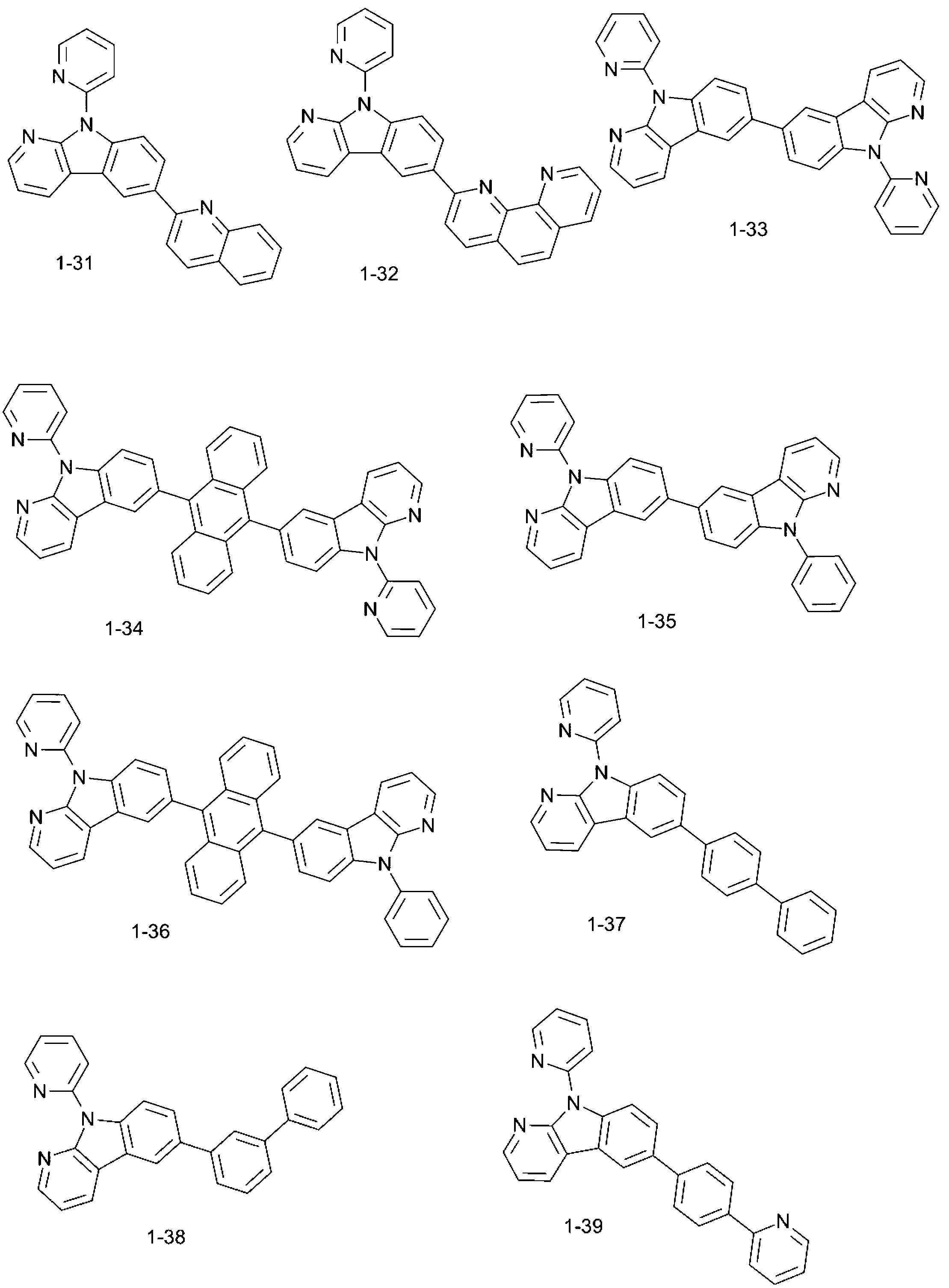
상기 카바졸 화합물은 제한되지 않으나 하기 1-1 내지 1-102로 표시되는 화합물 중 어느 하나일 수 있다.The carbazole compound is not limited, but may be any one of compounds represented by 1-1 to 1-102 below.


본 발명의 일 실시예에 따른 카바졸 화합물은 전술한 반응기들, 특히 질소를 헤테로원자로 하는 반응기들을 함유함으로써, 양극성(bipolarity) 특성을 가진다. 이로 인해, HOMO(Highest Occupied Molecular Orbital)와 LUMO(Lowest Unoccupied Molecular Orbital) 에너지 준위가 용이하게 조절되어 유기발광소자의 구동 전압을 낮출 수 있으므로, 본 발명의 일 실시예에 따른 카바졸 화합물은 유기발광소자의 전자수송층이나 텐덤형(tandem) 유기발광소자의 n형 전하생성층의 재료로서 우수한 특성을 갖는다. The carbazole compound according to an embodiment of the present invention contains the above-described reactors, particularly those having nitrogen as a heteroatom, and thus has a bipolarity characteristic. Accordingly, the energy level of the Highest Occupied Molecular Orbital (HOMO) and the Lowest Unoccupied Molecular Orbital (LUMO) can be easily adjusted to lower the driving voltage of the organic light emitting device, so that the carbazole compound according to an embodiment of the present invention is organic light emitting It has excellent properties as a material for an electron transport layer of a device or an n-type charge generation layer of a tandem organic light emitting device.
본 발명의 일 실시예에 따른 카바졸 화합물의 유리전이온도는 120℃ 이상이며, 용융온도가 290℃이상으로 열적 안정성이 우수하다. 이로 인해 고효율의 유기발광소자의 구현이 가능하다.The glass transition temperature of the carbazole compound according to an embodiment of the present invention is 120° C. or higher, and the melting temperature is 290° C. or higher, which has excellent thermal stability. Accordingly, it is possible to implement a highly efficient organic light emitting device.
도 1은 본 발명의 일 실시예에 따른 유기발광소자의 단면도이다. 도 1을 참조하면, 유기발광소자는 기판(110), 애노드(120), 유기물층(130) 및 캐소드(140)를 포함한다. 1 is a cross-sectional view of an organic light emitting device according to an embodiment of the present invention. Referring to FIG. 1, the organic light emitting device includes a
기판(110)은 유기 발광 표시 장치의 여러 엘리먼트들을 지지하고 보호하기 위한 기판이다. 기판(110)은 절연 물질로 구성될 수 있고, 예를 들어, 유리 또는 플라스틱 등으로 이루어질 수 있으나, 이에 제한되지 않고, 다양한 물질로 형성될 수 있다.The
애노드(120)는 정공을 공급하여야 하므로 일함수(work function)가 높은 도전성 물질로 형성된다. 애노드(120)는 일함수가 높은 투명 도전층을 포함할 수 있고, 투명 도전층은 투명 도전성 산화물(transparent conductive oxide, TCO)로 형성될 수 있으며, 예를 들어, ITO(indium tin oxide), IZO(indium zinc oxide), ITZO(indium tin zinc oxide), ZnO(zinc oxide)등으로 형성될 수 있다.Since the
유기물층(130)은 발광하기 위한 적층 구조로서, 단일 발광부 구조 또는 멀티 발광부 구조로 형성될 수 있다. 도 1에서는 단일 발광부 구조를 설명하고, 멀티 발광부 구조에 대해서는 도 2와 도 3을 참조하여 후술한다.The
단일 발광부 구조의 유기물층(130)은 정공주입층(131, hole injection layer, HIL), 정공수송층(132, hole transporting layer, HTL), 발광층(133), 전자수송층(134, electron transporting layer, ETL) 및 전자주입층(135, electron injection layer, EIL)이 적층된 구조로 이루어질 수 있다. The
정공주입층(131)은 애노드(120)로부터 발광층(133)으로 정공의 주입을 용이하게 한다. 예를 들어, PANI(polyaniline), NPD(N,N-dinaphthyl-N,N'-diphenyl benzidine), CuPc(cupper phthalocyanine) 및 PEDOT(poly(3,4)-ethylenedioxythiophene) 등으로부터 선택될 수 있으며, 이에 한정되는 것은 아니다.The
정공수송층(132)은 정공의 수송을 용이하게 한다. 예를 들어 NPD(N, N-dinaphthyl-N,N'-diphenyl benzidine), 및 TPD(N,N'-bis-(3-methylphenyl)-N,N'-bis-(phenyl)-benzidine) 등으로부터 선택될 수 있으며, 이에 한정되는 것은 아니다..The
발광층(133)은 특정 파장의 빛을 발광한다. 발광층(133)은 호스트와 호스트에 포함되는 다양한 도펀트로 이루어진다. 청색 파장의 빛을 발광시키기 위해 안트라센계열 블루 호스트와 파이렌계열 도판트를 사용할 수 있다. 예를 들어, ADN(9,10-di(2-naphthyl)anthracene), CBP(4, 4′-N, N′-dicarbazolbiphenyl), DPVBi(4,4'-bis(2,2-diphenylethen-1-yl)-diphenyl) 등으로부터 선택될 수 있으며, 이에 한정되는 것은 아니다. 도펀트는 발광되는 빛이 원하는 파장을 갖도록 다양한 물질이 이용된다. 예를 들어, 도펀트의 물질은 청색 파장의 빛을 발광시키기 위해 1,6-Bis(diphenylamine)pyrene, TBPe(tetrakis(t-butyl)perylene) 등으로부터 선택될 수 있으며, 적색 파장의 빛을 발광시키기 위해 Ir(piq)2acac(Bis(1-phenylisoquinoline)(acetylacetonate)iridium (III)), 녹색 파장의 빛을 발광시키기 위해, Irppy3(fac-tris(2-pheny-lpyridine)iridium) 등으로부터 선택될 수 있다.The
전자수송층(134)은 발광층(133) 상에 형성되며, 전자의 수송을 용이하게 하며, 상기 화학식 1로 표시된 카바졸 화합물을 함유하여 이루어질 수 있다. 전자수송층(134)이 상기 화학식 1로 표시된 카바졸 화합물을 함유하는 경우, 전술한 바와 같이 유기발광소자의 구동 전압이 감소되고, 효율과 수명이 향상될 수 있다.The
전자수송층(134) 상에 형성되는 전자주입층(135)은 전자의 주입을 용이하게 한다. Alq3(tris(8-hydroxyquinolino)aluminum), TAZ(3-phenyl-4-(1-naphthyl)-5-phenyl-1,2,4-triazole), Balq(bis (2-methyl-8-quinolinate) 등으로부터 선택될 수 있으며, 이에 한정되는 것은 아니다. 실시예에 따라 MgF2, LiF, NaF, KF, RbF, CsF, FrF 및 CaF2등과 같은 금속할라이드(metal halide) 화합물로 형성될 수도 있다.The
캐소드(140)는 발광층(133) 상에 형성된다. 캐소드(140)는 전자를 공급하여야 하므로, 전기 전도도가 높고 일함수가 낮은 물질로 형성된다. 예를 들어, 캐소드(140)는 은(Ag), 티타늄(Ti), 알루미늄(Al), 금(Au), 몰리브덴(Mo), 또는 은(Ag)과 마그네슘(Mg)의 합금 등과 같은 금속성 물질로 형성될 수 있으며, 실시예에 따라 ITO, IZO 등으로도 형성될 수 있으며, 이에 한정되는 것은 아니다. The
도 2는 본 발명의 다른 실시예에 따른 tandem형 유기발광소자의 단면도이다. 도 2를 참조하면, 유기발광소자는 기판(210), 애노드(220), 유기물층(230) 및 캐소드(240)를 포함한다. 도 2의 기판(210), 애노드(220), 캐소드(240)는 도 1의 기판(110), 애노드(120) 캐소드(140)와 실질적으로 동일한바, 중복하여 설명되지 않는다.2 is a cross-sectional view of a tandem type organic light emitting device according to another embodiment of the present invention. Referring to FIG. 2, the organic light emitting device includes a
유기물층(230)은 제1 발광부(231), 전하생성층(232) 및 제2 발광부(233)를 포함한다. 제1 발광부(231)는 정공주입층, 정공수송층, 발광층, 전자수송층을 포함하고, 제2 발광부(233)는 정공수송층, 발광층, 전자수송층 및 전자주입층을 포함한다. 제1 발광부(231)는 예컨대 청색(Blue)의 빛을 발광하도록 구성될 수 있으며, 제2 발광부(233)는 녹색(Green) 또는 황색-녹색(Yellow-Green)의 빛을 발광하도록 구성될 수 있다.The
또한, 도 2에서 제1 발광부(231) 및 제2 발광부(233)의 전자수송층은 상기 화학식 1로 표시된 카바졸 화합물을 함유할 수 있다. 예를 들어, TmPyPb(1,3,5-tri (m-pyrid-3-yl-phenyl) benzene), Alq3, TAZ, BAlq 등으로부터 선택될 수 있으며, 이에 한정되는 것은 아니다. 한편, 제1 발광부(231) 상에는 전하생성층(232)이 형성된다. 전하생성층(232)은 n형 전하생성층 및 p형 전하생성층이 적층되어 이루어진다. 전하생성층(232)은 전하를 생성하거나, 정공 및 전자로 분리하여 제1 발광부(231)와 제2 발광부(233)에 전하를 주입한다. n형 전하생성층은 애노드(220)에 인접한 제1 발광부(231)의 발광층에 전자를 공급하고, p형 전하생성층은 캐소드(240)에 인접한 제2 발광부(233)의 발광층에 정공을 공급한다. 이에 따라, 복수의 발광부를 갖는 유기발광소자의 발광 효율이 높게 유지되며, 구동 전압을 낮출 수 있다.In addition, in FIG. 2, the electron transport layers of the first
여기서, n형 전하생성층은 본 발명의 일 실시예에 따른 상기 화학식 1로 표시된 카바졸 화합물로 이루어진다. n형 전하생성층이 본 개시의 카바졸 화합물로 이루어짐으로써, n형 전하생성층과 p형 전하생성층 사이의 에너지 레벨 차이를 최소화하여 제1 발광부(231)에 전자 주입량을 향상시켜 구동 전압을 향상시킬 수 있다. 또한, n형 전하생성층이 알칼리 금속으로 도핑된 경우에도, 알칼리 금속이 p형 전하생성층으로 확산되는 현상을 최소화하여 유기발광소자의 수명을 개선할 수 있다.Here, the n-type charge generation layer is made of the carbazole compound represented by Formula 1 according to an embodiment of the present invention. Since the n-type charge generation layer is made of the carbazole compound of the present disclosure, the difference in the energy level between the n-type charge generation layer and the p-type charge generation layer is minimized to increase the amount of electrons injected into the first
도 3은 본 발명의 또 다른 실시예에 따른 템덤형(tandem) 유기발광소자의 단면도이다. 도 3을 참조하면, 유기발광소자는 기판(210), 애노드(220), 유기물층(230) 및 캐소드(240)를 포함한다. 도 3의 기판(210), 애노드(220), 캐소드(240)는 도 1의 기판(110), 애노드(120), 캐소드(140)와 실질적으로 동일한바, 중복하여 설명되지 않는다.3 is a cross-sectional view of a tandem organic light-emitting device according to another embodiment of the present invention. Referring to FIG. 3, the organic light emitting device includes a
유기물층(230)은 제1 발광부(231), 제1 전하생성층(232), 제2 발광부(233), 제2 전하생성층(234) 및 제3 발광부(235)가 적층된 층이다. 도 3에서 제1 발광부(231), 제1 전하생성층(232), 제2 발광부(233)는 도 2에서의 제1 발광부(231), 전하생성층(232), 제2 발광부(233)와 실질적으로 동일할 수 있다. 다만, 도 3에서는 예를 들어, 제1 발광부(231)는 청색(Blue) 빛을 발광하도록 구성되고, 제2 발광부(233)는 황색-녹색(Yellow-Green) 빛을 발광하도록 구성되고, 제3 발광부(235)는 청색(Blue) 빛을 발광하도록 구성될 수 있다.The
제2 발광부(233) 상에 형성된 제2 전하생성층(234)도 n형 전하생성층과 p형 전하생성층으로 이루어지고, n형 전하생성층은 상기 화학식 1로 표시된 카바졸 화합물로 이루어진다. n형 전하생성층이 본 개시의 카바졸 화합물로 이루어짐으로써, n형 전하생성층과 p형 전하생성층 사이의 에너지 레벨 차이를 최소화하여 제2 발광부(233)에 전자 주입량을 향상시켜 구동 전압을 향상시킬 수 있다. 또한, n형 전하생성층이 알칼리 금속으로 도핑된 경우에도, 알칼리 금속이 p형 전하생성층으로 확산되는 현상을 최소화하여 유기발광소자의 수명을 개선할 수 있다.The second
이하에서는 상기 화합물 1-51, 1-49, 1-4의 제조예 및 유기발광소자의 실시예 1, 2, 3 및 비교예 1의 제조예를 설명한다. 다만, 하기에 기재된 제조예들은 본 발명을 구체적으로 예시하거나 설명하기 위한 것일 뿐이며, 이하에 기재된 제조예들에 의해 본 발명을 제한하여 해석되어서는 안된다.Hereinafter, preparation examples of compounds 1-51, 1-49, and 1-4 and preparation examples of Examples 1, 2, and 3 and Comparative Example 1 of the organic light-emitting device will be described. However, the preparation examples described below are only intended to specifically illustrate or explain the present invention, and should not be interpreted to limit the present invention by the preparation examples described below.
1. 화합물 1-51의 1. Of compound 1-51 제조예Manufacturing example
상기 화합물 1-51로 표시된 6-(10-(naphthalen-3-yl)anthracen-9-yl)-9-(pyridin-2-yl)-9H-pyrido[2,3-b]indole을 아래와 같은 반응들을 이용해 제조하였다.
6-(10-(naphthalen-3-yl)anthracen-9-yl)-9-(pyridin-2-yl)-9H-pyrido[2,3-b]indole represented by compound 1-51 as follows Prepared using reactions.
(1) 중간체 A (6-bromo-9-(pyridin-2-yl)-9H-pyrido[2,3-b]indole) 합성(1) Synthesis of Intermediate A (6-bromo-9-(pyridin-2-yl)-9H-pyrido[2,3-b]indole)

둥근바닥 플라스크에 6-bromo-9H-pyrido[2,3-b]indole(10g, 40mmol), 2-Iodopyridine(12.4g, 61mmol), CuI(9.2g, 49mmol), trans-1,2-dicyclohexanediamine(1.8g, 16mmol), K3PO4(34.4g, 162mmol)을 1,4-dioxane에 녹인후 12시간동안 환류교반시켰다. 반응 종료 후 감압증류하여 용매를 제거하였다. 용매 제거 후 컬럼정제(Hexane:MC=3:1)를 하고 용매를 제거한 후 MC/Pet.Ether를 사용하여 침전시켜 6g(수율 45.7%)를 수득하였다.
6-bromo-9H-pyrido[2,3-b]indole(10g, 40mmol), 2-Iodopyridine(12.4g, 61mmol), CuI(9.2g, 49mmol), trans-1,2-dicyclohexanediamine in a round bottom flask (1.8g, 16mmol), K 3 PO 4 (34.4g, 162mmol) was dissolved in 1,4-dioxane and stirred under reflux for 12 hours. After completion of the reaction, the solvent was removed by distillation under reduced pressure. After removing the solvent, column purification (Hexane:MC=3:1) was carried out, and after removing the solvent, 6g (yield 45.7%) was obtained by precipitation using MC/Pet.Ether.
(2) 화합물 1-51 (6-(10-(naphthalen-3-yl)anthracen-9-yl)-9-(pyridin-2-yl)-9H-pyrido[2,3-b]indole) 합성(2) Synthesis of compound 1-51 (6-(10-(naphthalen-3-yl)anthracen-9-yl)-9-(pyridin-2-yl)-9H-pyrido[2,3-b]indole)

질소분위기 하의 둥근바닥 플라스크에 중간체 A(3g, 9mmol), 9-(naphthalen-2-yl)anthracen-10-boronic acid(3.5g, 10mmol), Tetrakis(triphenylphosphine) palladium(0)(0.4g, 0.4mmol), Toluene 60ml, EtOH 15ml, 2M K2CO3 10ml을 넣고 12시간동안 환류 교반시켰다. 반응 종료 후 여과하여 크루드(crude) 상태의 침전물을 얻었다. 크루드 침전물을 MC로 컬럼 분리 하였고 용매를 제거한 후 재결정을 하여 상기 화합물 1-51 3g(수율 59%)을 수득하였다.
Intermediate A (3g, 9mmol), 9-(naphthalen-2-yl)anthracen-10-boronic acid (3.5g, 10mmol), Tetrakis(triphenylphosphine) palladium(0)(0.4g, 0.4) in a round bottom flask under nitrogen atmosphere. mmol), Toluene 60ml, EtOH 15ml, 2M K 2 CO 3 10ml was added and stirred under reflux for 12 hours. After the reaction was completed, the precipitate was filtered to obtain a crude precipitate. The crude precipitate was separated by column using MC, and the solvent was removed and recrystallized to obtain 3g (yield 59%) of the compound 1-51.
2. 화합물 1-49의 2. of compound 1-49 제조예Manufacturing example
상기 화합물 1-49로 표시된 6-(10-phenylanthracen-9-yl)-9-(pyridin-2-yl)-9H-pyrido[2,3-b]indole을 아래와 같은 반응을 이용해 제조하였다.6-(10-phenylanthracen-9-yl)-9-(pyridin-2-yl)-9H-pyrido[2,3-b]indole represented by Compound 1-49 was prepared using the following reaction.

질소분위기 하의 둥근바닥 플라스크에 중간체 A(3g, 9mmol), 9-phenylanthracen-10-boronic acid(3g, 10mmol), Tetrakis(triphenylphosphine) palladium(0)(0.4g, 0.4mmol), Toluene 60ml, EtOH 15ml, 2M K2CO3 10ml을 넣고 12시간 동안 환류 교반시켰다. 반응 종료 후 여과하여 크루드(crude) 상태의 침전물을 얻었다. 크루드 침전물을 MC로 컬럼 분리 하였고 용매를 제거한 후 재결정을 하여 상기 화합물 1-49 2.5g(수율 54%)을 수득하였다.
In a round bottom flask under nitrogen atmosphere, Intermediate A (3g, 9mmol), 9-phenylanthracen-10-boronic acid (3g, 10mmol), Tetrakis (triphenylphosphine) palladium (0) (0.4g, 0.4mmol), Toluene 60ml, EtOH 15ml , 2M K 2 CO 3 10ml was added and stirred under reflux for 12 hours. After the reaction was completed, the precipitate was filtered to obtain a crude precipitate. Crude precipitate was separated by column using MC, and the solvent was removed and recrystallized to obtain 2.5 g of compound 1-49 (yield 54%).
3. 화합물 1-4의 3. Of compound 1-4 제조예Manufacturing example
상기 화합물 1-4로 표시된 1-(9-phenyl-9H-pyrido[2,3-b]indol-6-yl)ethanone을 아래와 같은 반응들을 이용해 제조하였다.
1-(9-phenyl-9H-pyrido[2,3-b]indol-6-yl)ethanone represented by Compound 1-4 was prepared using the following reactions.
(1) 중간체 B (1-(9H-pyrido[2,3-b]indol-6-yl)ethanone) 합성(1) Synthesis of intermediate B (1-(9H-pyrido[2,3-b]indol-6-yl)ethanone)

둥근바닥 플라스크에 α-carboline(10g, 59mmol), AlCl3(15.9g, 119mol)을 MC에 녹인 후 6시간동안 환류교반시켰다. 반응 종료 후 감압증류하여 용매를 제거하였다. 용매 제거 후 컬럼정제(Hexane:MC=3:1)를 하고 용매를 제거하여 중간체 B 8g(수율 64%)을 수득하였다.
In a round bottom flask, α-carboline (10g, 59mmol), AlCl 3 (15.9g, 119mol) was dissolved in MC and stirred under reflux for 6 hours. After completion of the reaction, the solvent was removed by distillation under reduced pressure. After removing the solvent, column purification (Hexane:MC=3:1) was performed, and the solvent was removed to obtain 8 g of intermediate B (64% yield).
(2) 중간체 C (1-(9-phenyl-9H-pyrido[2,3-b]indol-6-yl)ethanone) 합성(2) Synthesis of intermediate C (1-(9-phenyl-9H-pyrido[2,3-b]indol-6-yl)ethanone)

둥근바닥 플라스크에 중간체 B(5g, 24mmol), Iodobenzene(7.3g, 36mmol), CuI(5.4g, 29mmol), trans-1,2-dicyclohexanediamine(1.1g, 10mmol), K3PO4(20.2g, 95mmol)을 1,4-dioxane에 녹인 후 12시간동안 환류교반시켰다. 반응 종료 후 감압증류하여 용매를 제거하였다. 용매 제거 후 컬럼정제(Hexane:MC=3:1)를 하고 용매를 제거한 후 MC/Pet.Ether를 사용하여 침전시켜 중간체 C 3g(수율 44%)을 수득하였다.
In a round bottom flask, intermediate B (5g, 24mmol), Iodobenzene (7.3g, 36mmol), CuI (5.4g, 29mmol), trans-1,2-dicyclohexanediamine (1.1g, 10mmol), K 3 PO 4 (20.2 g, 95mmol) was dissolved in 1,4-dioxane and stirred under reflux for 12 hours. After completion of the reaction, the solvent was removed by distillation under reduced pressure. After removal of the solvent, column purification (Hexane:MC=3:1) was performed, and after removing the solvent, 3g (yield 44%) of intermediate C was obtained by precipitation using MC/Pet.Ether.
(3) 화합물 1-4 (1-(9-phenyl-9H-pyrido[2,3-b]indol-6-yl)ethanone) 합성(3) Synthesis of compound 1-4 (1-(9-phenyl-9H-pyrido[2,3-b]indol-6-yl)ethanone)

둥근바닥 플라스크에 중간체 C(3g, 12mmol), 8-aminoquinoline-7-carbaldehyde(5g, 24mmol), KOH(10.3g, 49mmol)를 Toluene, EtOH 에 녹인 후 12시간동안 환류 교반한다. 반응 종료 후 반응액을 냉각 후 Silicagel로 여과한 후 여액을 감압 농축하여 용매를 제거한다. 농축물을 컬럼정제(MC→MC:MeOH=50:1)한 후 감압농축한 후 MeOH로 세척하여 화합물 1-4 2g(수율 33%)을 수득하였다.
Intermediate C (3g, 12mmol), 8-aminoquinoline-7-carbaldehyde (5g, 24mmol), and KOH (10.3g, 49mmol) were dissolved in Toluene and EtOH in a round bottom flask and stirred under reflux for 12 hours. After completion of the reaction, the reaction solution is cooled, filtered through Silicagel, and the filtrate is concentrated under reduced pressure to remove the solvent. The concentrate was purified by column (MC→MC:MeOH=50:1), concentrated under reduced pressure, and washed with MeOH to give 2g (yield 33%) of compound 1-4.
4. 4. 실시예Example 1의 Of 1 제조예Manufacturing example
ITO(Indium tin oxide)가 1000Å 두께로 기판 상에 증착되였다. 정공주입층으로 HAT-CN을 50Å 두께로 증착하고, 상기 정공주입층 상에 정공수송층으로 NPD를 1200Å 두께로 증착하였다. 다음으로, 상기 정공주입층 상에 발광층을 형성하였다. 발광층은 AND를 호스트로 하여 안트라센계 화합물을 도펀트로하여 200Å 두께로 증착되었다. 이어서 전자수송층으로 TmPyPb을 100Å 두께로 증착하였다. n형 전하생성층은 상기 화합물 1-51을 100Å 두께로 증착하였다. p형 전하생성층은 HAT-CN을 200Å 두께로, 정공수송층은 NPD를 1200Å 두께로, 다음 발광층은 CBP를 호스트, Ir계 물질을 도펀트로 하여 200Å 두께로 형성하였다. 두번째 발광층 상의 전자수송층과 전자주입층 각각은 Alq3과 LiF를 사용하여 형성하였으며, 캐소드는 Al을 2000Å 두께로 증착하였다.
Indium tin oxide (ITO) was deposited on the substrate to a thickness of 1000Å. HAT-CN was deposited to a thickness of 50 Å as a hole injection layer, and NPD was deposited to a thickness of 1200 Å as a hole transport layer on the hole injection layer. Next, a light emitting layer was formed on the hole injection layer. The light emitting layer was deposited to a thickness of 200 Å using AND as a host and an anthracene compound as a dopant. Subsequently, TmPyPb was deposited to a thickness of 100 Å as an electron transport layer. For the n-type charge generation layer, Compound 1-51 was deposited to a thickness of 100 Å. The p-type charge generation layer was formed to a thickness of 200 Å of HAT-CN, the NPD of the hole transport layer to a thickness of 1200 Å, and the next emission layer was formed to a thickness of 200 Å using CBP as a host and an Ir-based material as a dopant. Each of the electron transport layer and the electron injection layer on the second emission layer was formed using Alq 3 and LiF, and the cathode was deposited with Al to a thickness of 2000 Å.
5. 5. 실시예Example 2의 Of 2 제조예Manufacturing example
n형 전하생성층을 상기 화합물 1-49로 형성한 것을 제외하고는 동일한 조건으로 유기발광소자를 제조하였다.
An organic light-emitting device was manufactured under the same conditions except that the n-type charge generation layer was formed of Compound 1-49.
5. 5. 실시예Example 3의 Of 3 제조예Manufacturing example
n형 전하생성층을 상기 화합물 1-4로 형성한 것을 제외하고는 동일한 조건으로 유기발광소자를 제조하였다.
An organic light-emitting device was manufactured under the same conditions, except that the n-type charge generation layer was formed of the compound 1-4.
6. 6. 비교예Comparative example 1의 Of 1 제조예Manufacturing example
n형 전하생성층을 BPhen(4,7-diphenyl-1,10- phenanthroline)으로 형성한 것을 제외하고는 동일한 조건으로 유기발광소자를 제조하였다.
An organic light emitting device was manufactured under the same conditions except that the n-type charge generation layer was formed of BPhen (4,7-diphenyl-1,10-phenanthroline).
이하에는 상기 실시예 1 내지 3 및 비교예 1의 유기발광소자의 구동 전압 효율, 색좌표 및 수명을 측정하여 이하의 표 1에 나타내었다. 또한, 구동 전압에 따른 전류 밀도를 측정하여 도 4에 나타내었으며, 시간에 따른 휘도 변화량을 측정하여 도 5에 나타내었다. Hereinafter, the driving voltage efficiency, color coordinates, and lifetime of the organic light-emitting devices of Examples 1 to 3 and Comparative Example 1 were measured and shown in Table 1 below. In addition, the current density according to the driving voltage was measured and shown in FIG. 4, and the amount of change in luminance over time was measured and shown in FIG.
도 4를 참조하면, 실시예 1, 2 및 3의 구동 전압에 따른 전류 밀도가 비교예 1과 비교하여 향상된 것을 알 수 있다. 또한, 도 5를 참조하면, 시간에 따른 휘도 변화량이 비교예 1과 비교하여 실시예 1, 2 및 3에서 월등히 향상된 것을 알 수 있다. 표 1에서는 구동 전압의 감소를 백분율로 표시하였다. Referring to FIG. 4, it can be seen that the current density according to the driving voltage of Examples 1, 2, and 3 is improved compared to Comparative Example 1. Further, referring to FIG. 5, it can be seen that the amount of luminance change over time was significantly improved in Examples 1, 2, and 3 compared to Comparative Example 1. In Table 1, the decrease in the driving voltage is expressed as a percentage.
[표 1][Table 1]

상기 표 1에 나타나는 바와 같이, 실시예 1 내지 3의 유기발광소자는 비교예 1과 실질적으로 동일한 색좌표(CIEx, CIEy)를 나타내면서, 구동 전압에 따른 전류 밀도가 5 내지 7% 향상되고, 수명 특성이 10% 내지 56% 향상되었다.As shown in Table 1, the organic light-emitting devices of Examples 1 to 3 exhibit substantially the same color coordinates (CIEx, CIEy) as in Comparative Example 1, and the current density according to the driving voltage is improved by 5 to 7%, and the lifespan characteristics This was improved by 10% to 56%.
이하에는, 제조예 1, 2 및 3으로 제조된 카바졸 화합물의 유리전이온도와 용융온도를 측정하여 도 6a 내지 6c 및 이하의 표 2에 나타내었다.In the following, the glass transition temperature and melting temperature of the carbazole compounds prepared in Preparation Examples 1, 2 and 3 were measured, and are shown in FIGS.
[표 2][Table 2]

도 6a의 (a)를 참조하면, 화합물 1-51은 약 163℃에서 유리전이온도를 가지며, 도 6a의 (b)를 참조하면 약 352℃의 용융온도를 가진다. 도 6b의 (a)를 참조하면, 화합물 1-49는 약 145℃에서 유리전이온도를 가지며, 도 6b의 (b)를 참조하면 약 332℃의 용융온도를 가진다. 도 6c의 (a)를 참조하면, 화합물 1-4는 약 124℃에서 유리전이온도를 가지며, 도 6c의 (b)를 참조하면 약 289℃의 용융온도를 가진다.Referring to FIG. 6A(a), Compound 1-51 has a glass transition temperature of about 163°C, and referring to FIG. 6A(b), it has a melting temperature of about 352°C. Referring to (a) of FIG. 6B, Compound 1-49 has a glass transition temperature of about 145°C, and, referring to (b) of FIG. 6B, has a melting temperature of about 332°C. 6C(a), compound 1-4 has a glass transition temperature of about 124°C, and referring to FIG. 6C(b), it has a melting temperature of about 289°C.
본 발명의 일 실시예에 따른 카바졸 화합물은 높은 유리전이온도와 용융온도를 가져 열적 안정성이 우수하다. 이로 인해 고효율의 유기발광소자의 구현이 가능하다.The carbazole compound according to an embodiment of the present invention has high glass transition ionicity and melting temperature, and thus has excellent thermal stability. Accordingly, it is possible to implement a highly efficient organic light emitting device.
이상 첨부된 도면을 참조하여 본 발명의 실시예들을 더욱 상세하게 설명하였으나, 본 발명은 반드시 이러한 실시예로 국한되는 것은 아니고, 본 발명의 기술사상을 벗어나지 않는 범위 내에서 다양하게 변형 실시될 수 있다. 따라서, 본 발명에 개시된 실시예들은 본 발명의 기술 사상을 한정하기 위한 것이 아니라 설명하기 위한 것이고, 이러한 실시예에 의하여 본 발명의 기술 사상의 범위가 한정되는 것은 아니다. 그러므로, 이상에서 기술한 실시예들은 모든 면에서 예시적인 것이며 한정적이 아닌 것으로 이해해야만 한다. 본 발명의 보호 범위는 아래의 청구범위에 의하여 해석되어야 하며, 그와 동등한 범위 내에 있는 모든 기술 사상은 본 발명의 권리범위에 포함되는 것으로 해석되어야 할 것이다.Although the embodiments of the present invention have been described in more detail with reference to the accompanying drawings, the present invention is not necessarily limited to these embodiments, and various modifications can be made without departing from the spirit of the present invention. . Accordingly, the embodiments disclosed in the present invention are not intended to limit the technical idea of the present invention, but to explain the technical idea, and the scope of the technical idea of the present invention is not limited by these embodiments. Therefore, it should be understood that the embodiments described above are illustrative in all respects and not limiting. The scope of protection of the present invention should be interpreted by the following claims, and all technical ideas within the scope equivalent thereto should be interpreted as being included in the scope of the present invention.
110, 210: 기판
120, 220: 애노드
130, 230: 유기물층
131: 정공주입층
132: 정공수송층
133: 발광층
134: 전자수송층
135: 전자주입층
140, 240: 캐소드
231: 제1 발광부
232: 전하생성층
233: 제2 발광부
234: 제2 전하생성층
235: 제3 발광부110, 210: substrate
120, 220: anode
130, 230: organic material layer
131: hole injection layer
132: hole transport layer
133: light emitting layer
134: electron transport layer
135: electron injection layer
140, 240: cathode
231: first light emitting unit
232: charge generation layer
233: second light emitting unit
234: second charge generation layer
235: third light emitting unit
Claims (13)
상기 애노드 상에 배치되고 제1 발광층을 포함하는 제1 발광부;
상기 제1 발광부 상에 배치되는 n형 전하생성층 및 상기 n형 전하생성층 상에 배치되는 p형 전하생성층을 포함하는 제1 전하생성층;
상기 제1 전하생성층 상에 배치되고 제2 발광층을 포함하는 제2 발광부; 및
상기 제2 발광부 상에 배치되는 캐소드를 포함하고,
상기 n형 전하생성층은 하기 화합물들 중 하나의 화합물을 포함하는, 유기발광소자.


A first light-emitting unit disposed on the anode and including a first light-emitting layer;
A first charge generation layer including an n-type charge generation layer disposed on the first light emitting part and a p-type charge generation layer disposed on the n-type charge generation layer;
A second light-emitting unit disposed on the first charge generation layer and including a second light-emitting layer; And
Including a cathode disposed on the second light emitting portion,
The n-type charge generation layer comprises one of the following compounds, an organic light emitting device.
상기 n형 전하생성층은 알칼리 금속이 도핑된 것을 특징으로 하는, 유기발광소자. The method of claim 1,
The organic light emitting device, characterized in that the n-type charge generation layer is doped with an alkali metal.
상기 제1 발광부 및 상기 제2 발광부는 전자수송층을 포함하는 것을 특징으로 하는, 유기발광소자.The method of claim 1,
The organic light-emitting device, characterized in that the first light-emitting unit and the second light-emitting unit include an electron transport layer.
상기 전자수송층은 상기 화합물을 포함하는 것을 특징으로 하는, 유기발광소자.The method of claim 10,
The electron transport layer is an organic light emitting device, characterized in that containing the compound.
상기 제2 발광부 상에 배치되는 n형 전하 생성층 및 상기 n형 전하 생성층 상에 배치되는 p형 전하생성층을 포함하는 제2 전하생성층; 및 상기 제2 전하생성층 상에 배치되고, 제3 발광층을 포함하는 제3 발광부를 더 포함하는 것을 특징으로 하는, 유기발광소자.The method of claim 1,
A second charge generation layer including an n-type charge generation layer disposed on the second light emitting part and a p-type charge generation layer disposed on the n-type charge generation layer; And a third light emitting unit disposed on the second charge generation layer and including a third light emitting layer.
상기 제2 전하생성층의 n형 전하 생성층은 상기 화합물을 포함하는 것을 특징으로 하는, 유기발광소자. The method of claim 12,
An organic light emitting device, characterized in that the n-type charge generation layer of the second charge generation layer contains the compound.
Priority Applications (4)
| Application Number | Priority Date | Filing Date | Title |
|---|---|---|---|
| KR1020140038217A KR102192001B1 (en) | 2014-03-31 | 2014-03-31 | Carbazole compound and organic light emitting diode including the same |
| EP15160734.8A EP2927978B1 (en) | 2014-03-31 | 2015-03-25 | Organic light-emitting diode |
| US14/673,078 US10290814B2 (en) | 2014-03-31 | 2015-03-30 | Organic light-emitting diode |
| CN201510145747.0A CN104953037B (en) | 2014-03-31 | 2015-03-30 | Organic light-emitting diode |
Applications Claiming Priority (1)
| Application Number | Priority Date | Filing Date | Title |
|---|---|---|---|
| KR1020140038217A KR102192001B1 (en) | 2014-03-31 | 2014-03-31 | Carbazole compound and organic light emitting diode including the same |
Publications (2)
| Publication Number | Publication Date |
|---|---|
| KR20150113754A KR20150113754A (en) | 2015-10-08 |
| KR102192001B1 true KR102192001B1 (en) | 2020-12-16 |
Family
ID=52706081
Family Applications (1)
| Application Number | Title | Priority Date | Filing Date |
|---|---|---|---|
| KR1020140038217A Active KR102192001B1 (en) | 2014-03-31 | 2014-03-31 | Carbazole compound and organic light emitting diode including the same |
Country Status (4)
| Country | Link |
|---|---|
| US (1) | US10290814B2 (en) |
| EP (1) | EP2927978B1 (en) |
| KR (1) | KR102192001B1 (en) |
| CN (1) | CN104953037B (en) |
Families Citing this family (13)
| Publication number | Priority date | Publication date | Assignee | Title |
|---|---|---|---|---|
| US10096782B2 (en) | 2014-08-01 | 2018-10-09 | Lg Display Co., Ltd. | Organic light emitting display device |
| KR102469217B1 (en) * | 2015-11-27 | 2022-11-21 | 엘지디스플레이 주식회사 | Organic Light Emitting Diode Device |
| KR102439571B1 (en) * | 2015-12-03 | 2022-09-02 | 엘지디스플레이 주식회사 | organic light emitting device |
| KR102157756B1 (en) * | 2016-12-12 | 2020-09-18 | 엘지디스플레이 주식회사 | Organic compounds and organic light emitting diode and organic light emittind display device having the same |
| KR101984676B1 (en) * | 2017-11-07 | 2019-05-31 | 주식회사 진웅산업 | Phenanthroline compound and organic light emitting element comprising the same |
| KR101984677B1 (en) * | 2017-11-09 | 2019-05-31 | 주식회사 진웅산업 | phenanthroline compound and organic light emitting element comprising the same |
| CN109810123A (en) * | 2017-11-21 | 2019-05-28 | 北京鼎材科技有限公司 | Compound and its application in organic light emission field |
| CN109912592B (en) * | 2017-12-13 | 2022-05-17 | 江苏三月科技股份有限公司 | Compound containing pyridoindole and application of compound in organic electroluminescent device |
| CN109956939B (en) * | 2017-12-22 | 2023-02-17 | 北京鼎材科技有限公司 | Azacarbazole derivative, organic electroluminescence device containing same |
| CN109503576B (en) * | 2018-12-24 | 2020-11-24 | 武汉天马微电子有限公司 | Organic compound, display panel and display device |
| KR102239793B1 (en) * | 2019-04-25 | 2021-04-13 | 주식회사 진웅산업 | Phenanthroline compound and organic light emitting element comprising the same |
| KR20250016017A (en) * | 2023-07-24 | 2025-02-03 | 주식회사 진웅산업 | New compound and organic light emitting device comprising the same |
| CN119403357A (en) * | 2024-10-28 | 2025-02-07 | 京东方科技集团股份有限公司 | Organic light emitting diode, display substrate and display device |
Family Cites Families (15)
| Publication number | Priority date | Publication date | Assignee | Title |
|---|---|---|---|---|
| JP4541152B2 (en) * | 2002-12-12 | 2010-09-08 | 出光興産株式会社 | Material for organic electroluminescence device and organic electroluminescence device using the same |
| EP2479234B1 (en) * | 2008-05-13 | 2017-06-21 | Konica Minolta Holdings, Inc. | Organic electroluminescent element, display device and lighting device |
| US8603642B2 (en) * | 2009-05-13 | 2013-12-10 | Global Oled Technology Llc | Internal connector for organic electronic devices |
| KR101791276B1 (en) * | 2009-11-12 | 2017-10-27 | 호도가야 가가쿠 고교 가부시키가이샤 | Compound having a substituted anthracene ring structure and pyridoindole ring structure, and organic electroluminescent element |
| US9067919B2 (en) * | 2010-07-08 | 2015-06-30 | Basf Se | Use of dibenzofurans and dibenzothiophenes substituted by nitrogen-bonded five-membered heterocyclic rings in organic electronics |
| KR20120020901A (en) * | 2010-08-31 | 2012-03-08 | 롬엔드하스전자재료코리아유한회사 | Novel compounds for organic electronic material and organic electroluminescent device using the same |
| JP5761199B2 (en) * | 2010-10-22 | 2015-08-12 | コニカミノルタ株式会社 | Organic electroluminescence device |
| TWI538977B (en) * | 2011-02-07 | 2016-06-21 | Idemitsu Kosan Co | A double carbazole derivative and an organic electroluminescent element using the same |
| KR20130015370A (en) * | 2011-08-03 | 2013-02-14 | 엘지디스플레이 주식회사 | Phosphorescent material and organic electroluminescent device using the same |
| KR101474796B1 (en) | 2011-12-26 | 2014-12-19 | 제일모직주식회사 | Compound for organic optoelectronic device, organic light emitting diode including the same and display including the organic light emitting diode |
| CN103664746B (en) | 2012-09-03 | 2016-11-16 | 乐金显示有限公司 | Anthracene compound and comprise the Organic Light Emitting Diode of this anthracene compound |
| KR20140087806A (en) * | 2012-12-31 | 2014-07-09 | 제일모직주식회사 | COMPOUND FOR ORGANIC OPTOELECTRONIC DEVICE, ORGANIC LiGHT EMITTING DIODE INCLUDING THE SAME AND DISPLAY INCLUDING THE ORGANIC LiGHT EMITTING DIODE |
| KR101513987B1 (en) * | 2013-07-16 | 2015-04-21 | (주)더블유에스 | Aromatic amine derivative and organic electroluminescent device including the same |
| KR20140023406A (en) * | 2014-01-02 | 2014-02-26 | 롬엔드하스전자재료코리아유한회사 | Novel organic electroluminescent compounds and organic electroluminescent device using the same |
| US10096782B2 (en) * | 2014-08-01 | 2018-10-09 | Lg Display Co., Ltd. | Organic light emitting display device |
-
2014
- 2014-03-31 KR KR1020140038217A patent/KR102192001B1/en active Active
-
2015
- 2015-03-25 EP EP15160734.8A patent/EP2927978B1/en active Active
- 2015-03-30 US US14/673,078 patent/US10290814B2/en active Active
- 2015-03-30 CN CN201510145747.0A patent/CN104953037B/en active Active
Non-Patent Citations (1)
| Title |
|---|
| Angew. Chem. Int. Ed., Vol. 52, pp, 12696-12700(2013.10.07.)* |
Also Published As
| Publication number | Publication date |
|---|---|
| KR20150113754A (en) | 2015-10-08 |
| US10290814B2 (en) | 2019-05-14 |
| CN104953037B (en) | 2017-05-03 |
| CN104953037A (en) | 2015-09-30 |
| EP2927978B1 (en) | 2020-03-18 |
| US20150280141A1 (en) | 2015-10-01 |
| EP2927978A1 (en) | 2015-10-07 |
Similar Documents
| Publication | Publication Date | Title |
|---|---|---|
| KR102192001B1 (en) | Carbazole compound and organic light emitting diode including the same | |
| CN105321984B (en) | Organic light-emitting display device | |
| KR102268119B1 (en) | Pyrene compound and organic light emitting diode device comprising the same | |
| KR102187252B1 (en) | Anthracene composite and organic light emitting diode device comprising the same | |
| KR102000208B1 (en) | Organic light emitting device | |
| EP3174124B1 (en) | Organic light emitting display device | |
| KR101245243B1 (en) | Spiro Carbazole Compound And Organic Electronic Element Using The Same, Terminal Thereof | |
| KR20190080600A (en) | Organic light emitting diode | |
| KR20140146951A (en) | Organic light emitting device | |
| KR20110040874A (en) | Light emitting element | |
| KR20150007605A (en) | Iridium complex and Organic light emitting device comprising the same | |
| KR20140016653A (en) | Organic light emitting device comprising compounds | |
| KR101601679B1 (en) | Compound Containing 5-Membered Heterocycle And Organic Electronic Element Using The Same, Terminal Thereof | |
| KR20180032347A (en) | Compound for organic electronic element, organic electronic element comprising the same, and electronic device thereof | |
| KR101181277B1 (en) | Compound Containing Indoloacridine And Organic Electronic Element Using The Same, Terminal Thereof | |
| KR101270505B1 (en) | Amine Compound Having Three Carbazole And Organic Electronic Element Using The Same, Terminal Thereof | |
| KR20150064804A (en) | Compound and organic light emitting device comprising same | |
| CN105669555A (en) | Organic light emitting display device | |
| KR101497127B1 (en) | Compound Containing At Least Two 5-Membered Heterocycle And Organic Electronic Element Using The Same, Terminal Thereof | |
| KR101181276B1 (en) | Compound Containing Indoloacridine And Organic Electronic Element Using The Same, Terminal Thereof | |
| KR101181278B1 (en) | Compound Containing Indoloacridine And Organic Electronic Element Using The Same, Terminal Thereof | |
| KR102167047B1 (en) | Organometallic complex and organic light emitting device comprising same | |
| KR101497123B1 (en) | Compound Containing 5-Membered Heterocycle And Organic Electronic Element Using The Same, Terminal Thereof | |
| KR101077841B1 (en) | Cyclic Aromatic Compound AND ORGANIC ELECTRONIC ELEMENT USING THE SAME, TERMINAL THEREROF | |
| KR20140071805A (en) | Heterocyclic compound and organic light emitting device comprising the same |
Legal Events
| Date | Code | Title | Description |
|---|---|---|---|
| PA0109 | Patent application |
Patent event code: PA01091R01D Comment text: Patent Application Patent event date: 20140331 |
|
| PG1501 | Laying open of application | ||
| A201 | Request for examination | ||
| PA0201 | Request for examination |
Patent event code: PA02012R01D Patent event date: 20190116 Comment text: Request for Examination of Application Patent event code: PA02011R01I Patent event date: 20140331 Comment text: Patent Application |
|
| E902 | Notification of reason for refusal | ||
| PE0902 | Notice of grounds for rejection |
Comment text: Notification of reason for refusal Patent event date: 20200417 Patent event code: PE09021S01D |
|
| E701 | Decision to grant or registration of patent right | ||
| PE0701 | Decision of registration |
Patent event code: PE07011S01D Comment text: Decision to Grant Registration Patent event date: 20200923 |
|
| GRNT | Written decision to grant | ||
| PR0701 | Registration of establishment |
Comment text: Registration of Establishment Patent event date: 20201210 Patent event code: PR07011E01D |
|
| PR1002 | Payment of registration fee |
Payment date: 20201210 End annual number: 3 Start annual number: 1 |
|
| PG1601 | Publication of registration | ||
| PR1001 | Payment of annual fee |
Payment date: 20231115 Start annual number: 4 End annual number: 4 |
|
| PR1001 | Payment of annual fee |
Payment date: 20241118 Start annual number: 5 End annual number: 5 |