KR102157469B1 - System for reducing specific absorption rate - Google Patents
System for reducing specific absorption rate Download PDFInfo
- Publication number
- KR102157469B1 KR102157469B1 KR1020200088160A KR20200088160A KR102157469B1 KR 102157469 B1 KR102157469 B1 KR 102157469B1 KR 1020200088160 A KR1020200088160 A KR 1020200088160A KR 20200088160 A KR20200088160 A KR 20200088160A KR 102157469 B1 KR102157469 B1 KR 102157469B1
- Authority
- KR
- South Korea
- Prior art keywords
- cylindrical coil
- target
- absorption rate
- transfer target
- electromagnetic wave
- Prior art date
- Legal status (The legal status is an assumption and is not a legal conclusion. Google has not performed a legal analysis and makes no representation as to the accuracy of the status listed.)
- Active
Links
Images


Classifications
-
- H—ELECTRICITY
- H05—ELECTRIC TECHNIQUES NOT OTHERWISE PROVIDED FOR
- H05K—PRINTED CIRCUITS; CASINGS OR CONSTRUCTIONAL DETAILS OF ELECTRIC APPARATUS; MANUFACTURE OF ASSEMBLAGES OF ELECTRICAL COMPONENTS
- H05K1/00—Printed circuits
- H05K1/02—Details
- H05K1/0213—Electrical arrangements not otherwise provided for
- H05K1/0216—Reduction of cross-talk, noise or electromagnetic interference
-
- H—ELECTRICITY
- H01—ELECTRIC ELEMENTS
- H01F—MAGNETS; INDUCTANCES; TRANSFORMERS; SELECTION OF MATERIALS FOR THEIR MAGNETIC PROPERTIES
- H01F27/00—Details of transformers or inductances, in general
- H01F27/34—Special means for preventing or reducing unwanted electric or magnetic effects, e.g. no-load losses, reactive currents, harmonics, oscillations, leakage fields
-
- H—ELECTRICITY
- H05—ELECTRIC TECHNIQUES NOT OTHERWISE PROVIDED FOR
- H05K—PRINTED CIRCUITS; CASINGS OR CONSTRUCTIONAL DETAILS OF ELECTRIC APPARATUS; MANUFACTURE OF ASSEMBLAGES OF ELECTRICAL COMPONENTS
- H05K9/00—Screening of apparatus or components against electric or magnetic fields
- H05K9/0071—Active shielding
-
- H—ELECTRICITY
- H02—GENERATION; CONVERSION OR DISTRIBUTION OF ELECTRIC POWER
- H02J—ELECTRIC POWER NETWORKS; CIRCUIT ARRANGEMENTS OR SYSTEMS FOR SUPPLYING OR DISTRIBUTING ELECTRIC POWER; SYSTEMS FOR STORING ELECTRIC ENERGY
- H02J50/00—Circuit arrangements or systems for wireless supply or distribution of electric power
- H02J50/70—Circuit arrangements or systems for wireless supply or distribution of electric power involving the reduction of electric, magnetic or electromagnetic leakage fields
-
- H—ELECTRICITY
- H01—ELECTRIC ELEMENTS
- H01F—MAGNETS; INDUCTANCES; TRANSFORMERS; SELECTION OF MATERIALS FOR THEIR MAGNETIC PROPERTIES
- H01F27/00—Details of transformers or inductances, in general
- H01F27/28—Coils; Windings; Conductive connections
- H01F27/2804—Printed windings
-
- H—ELECTRICITY
- H01—ELECTRIC ELEMENTS
- H01F—MAGNETS; INDUCTANCES; TRANSFORMERS; SELECTION OF MATERIALS FOR THEIR MAGNETIC PROPERTIES
- H01F27/00—Details of transformers or inductances, in general
- H01F27/34—Special means for preventing or reducing unwanted electric or magnetic effects, e.g. no-load losses, reactive currents, harmonics, oscillations, leakage fields
- H01F27/36—Electric or magnetic shields or screens
- H01F27/363—Electric or magnetic shields or screens made of electrically conductive material
-
- H—ELECTRICITY
- H01—ELECTRIC ELEMENTS
- H01F—MAGNETS; INDUCTANCES; TRANSFORMERS; SELECTION OF MATERIALS FOR THEIR MAGNETIC PROPERTIES
- H01F38/00—Adaptations of transformers or inductances for specific applications or functions
- H01F38/14—Inductive couplings
-
- H—ELECTRICITY
- H02—GENERATION; CONVERSION OR DISTRIBUTION OF ELECTRIC POWER
- H02J—ELECTRIC POWER NETWORKS; CIRCUIT ARRANGEMENTS OR SYSTEMS FOR SUPPLYING OR DISTRIBUTING ELECTRIC POWER; SYSTEMS FOR STORING ELECTRIC ENERGY
- H02J50/00—Circuit arrangements or systems for wireless supply or distribution of electric power
- H02J50/50—Circuit arrangements or systems for wireless supply or distribution of electric power using additional energy repeaters between transmitting devices and receiving devices
-
- H04B5/0037—
-
- H—ELECTRICITY
- H04—ELECTRIC COMMUNICATION TECHNIQUE
- H04B—TRANSMISSION
- H04B5/00—Near-field transmission systems, e.g. inductive or capacitive transmission systems
- H04B5/70—Near-field transmission systems, e.g. inductive or capacitive transmission systems specially adapted for specific purposes
- H04B5/79—Near-field transmission systems, e.g. inductive or capacitive transmission systems specially adapted for specific purposes for data transfer in combination with power transfer
-
- H—ELECTRICITY
- H05—ELECTRIC TECHNIQUES NOT OTHERWISE PROVIDED FOR
- H05K—PRINTED CIRCUITS; CASINGS OR CONSTRUCTIONAL DETAILS OF ELECTRIC APPARATUS; MANUFACTURE OF ASSEMBLAGES OF ELECTRICAL COMPONENTS
- H05K1/00—Printed circuits
- H05K1/02—Details
- H05K1/0213—Electrical arrangements not otherwise provided for
- H05K1/0216—Reduction of cross-talk, noise or electromagnetic interference
- H05K1/023—Reduction of cross-talk, noise or electromagnetic interference using auxiliary mounted passive components or auxiliary substances
- H05K1/0233—Filters, inductors or a magnetic substance
-
- H—ELECTRICITY
- H05—ELECTRIC TECHNIQUES NOT OTHERWISE PROVIDED FOR
- H05K—PRINTED CIRCUITS; CASINGS OR CONSTRUCTIONAL DETAILS OF ELECTRIC APPARATUS; MANUFACTURE OF ASSEMBLAGES OF ELECTRICAL COMPONENTS
- H05K9/00—Screening of apparatus or components against electric or magnetic fields
- H05K9/0007—Casings
- H05K9/002—Casings with localised screening
- H05K9/0022—Casings with localised screening of components mounted on printed circuit boards [PCB]
Landscapes
- Engineering & Computer Science (AREA)
- Power Engineering (AREA)
- Microelectronics & Electronic Packaging (AREA)
- Computer Networks & Wireless Communication (AREA)
- Physics & Mathematics (AREA)
- Electromagnetism (AREA)
- Signal Processing (AREA)
- Shielding Devices Or Components To Electric Or Magnetic Fields (AREA)
Abstract
본 발명의 일 실시예에 의하면, 타겟 물질에 전자기파의 종파 특성을 이용하여 물성 변화를 유도하고, 물성 변화가 유도된 전사 타겟을 회로기판에 적용하여 전자파 흡수율를 저감시킬 수 있는 효과가 있다. 이와 관련하여 특히, 본 발명의 일 실시예는 제1 원통형 코일이 권선되어 내부에 소스 물질이 수용되고 제1 원통형 코일에 주기적 입력신호를 인가하여 소스 필드를 생성하는 소스 필드 생성부; 제1 원통형 코일에 인접하여 배치된 제2 원통형 코일이 권선되어 내부에 전사 타겟이 수용되고 생성된 소스 필드에 기반하여 전사 타겟의 물성을 변화시키는 물성 변화부; 및 전원이 연결되는 전원 인터페이스가 형성된 PCB 기판과 전원의 입력으로 전사 타겟이 타겟 필드를 형성하도록 제어하는 타겟 필드 회로부를 포함하는 전자파 흡수율 저감 시스템을 포함한다.According to an embodiment of the present invention, there is an effect of inducing a change in physical properties by using the longitudinal wave characteristics of an electromagnetic wave in a target material, and reducing an electromagnetic wave absorption rate by applying a transfer target from which the change in properties is induced to a circuit board. In this regard, in particular, an embodiment of the present invention includes a source field generator configured to generate a source field by winding a first cylindrical coil to receive a source material therein and applying a periodic input signal to the first cylindrical coil; A physical property change unit for winding a second cylindrical coil disposed adjacent to the first cylindrical coil to receive a transfer target therein and changing physical properties of the transfer target based on the generated source field; And a PCB substrate on which a power supply interface to which power is connected is formed, and a target field circuit unit that controls the transfer target to form a target field by an input of power.
Description
본 발명은 전자파 흡수율 저감 시스템에 관한 것이다.The present invention relates to an electromagnetic wave absorption rate reduction system.
현대를 살아가는 사람들은 무수히 많은 전기,전자 제품으로 원치 않는 전자파의 악영향을 받으며 살아가는 것이 일상이 되었다. 특히 텔레비젼, 컴퓨터 및 스마트폰은 일상 생활에서 뗄래야 뗄수 없는 필수품이 되었으며, 그로부터 방출되는 전자파에 대한 경각심은 어느 때보다도 높아지고 있는 추세이다. 특히,유선기기에서 무선기기로 바뀌어,무선주파수(wifi)환경에 장시간 노출되고 최근에는 고주파수(3.5GHz~28GHz) 빔포밍방식의 5G 서비스로 인한 높은 전자파 세기로 현대인의 건강은 위험에 처하게 되었다It has become a daily routine for people living in modern times to live under the adverse effects of unwanted electromagnetic waves with countless electrical and electronic products. In particular, TVs, computers, and smartphones have become indispensable necessities in everyday life, and the awareness of electromagnetic waves emitted from them is increasing more than ever. In particular, since wired devices have been changed to wireless devices, they are exposed to wireless frequency (wifi) environments for a long time, and in recent years, the health of modern people is at risk due to high electromagnetic wave strength due to 5G service of high frequency (3.5GHz~28GHz) beamforming method.
전자파의 인체 또는 생체 조직에 유해한 악영향과 관련해서, 세계보건기구(WHO) 산하 국제암연구소(IARC)에서는 휴대전화 전자파(RF)의 암 발생 등급을 2B로 분류하였으며, 전자파가 인체에 미칠 수 있는 또 다른 영향으로 크게 열작용과 비열작용 그리고 자극작용이 있을 수 있다고 하였다. 여기서 열작용은 주파수가 높고 강한 세기의 전자파에 인체가 노출되면 체온이 상승하여 세포나 조직의 기능에 영향을 주는 것을 말하며, 비열작용은 미약한 전자파에 장기간 노출되었을 때 발생하는 것이다. 그리고 자극작용이란 주파수가 낮고 강한 전자파에 노출되었을 때 인체에 유도된 전류가 신경이나 근육을 자극하는 것을 말한다.Regarding the harmful effects of electromagnetic waves on the human body or tissues, the International Cancer Research Institute (IARC) under the World Health Organization (WHO) classified the cancer incidence class of mobile phone electromagnetic waves (RF) as 2B. Another effect was that there could be large heat, specific heat, and stimulating effects. Here, the thermal action means that when the human body is exposed to high frequency and strong electromagnetic waves, the body temperature rises and affects the function of cells or tissues, and the specific heat action occurs when exposed to weak electromagnetic waves for a long time. And the stimulating action refers to the stimulation of nerves or muscles by the electric current induced in the human body when the frequency is low and exposed to strong electromagnetic waves.
종래 이러한 전자파의 흡수율를 저감시키기 위한 방법으로 대한민국 특허공개 제10-2004-0076737호에서는 휴대폰이 프런트 케이스에 도포되는 EMI 도료의 분포패턴을 최적화하여 SAR(Specific Absorption Rate)를 저감시키는 도포 방법을 개시하고 있고, 대한민국 특허등록 제10-1229058호에서는 전자파 차폐 및 열방출을 위한 동박 필름층 또는 그래핀 층을 형성하여 휴대폰의 후면에 부착형성함으로써, 휴대폰의 사용시 휴대폰으로부터 발생되는 전자파를 완전 흡수 또는 소멸시킬 수 있는 휴대폰 전자파 차단방법에 관하여 개시하고 있다.As a method for reducing the absorption rate of such electromagnetic waves, Korean Patent Laid-Open No. 10-2004-0076737 discloses a coating method for reducing SAR (Specific Absorption Rate) by optimizing the distribution pattern of EMI paint applied to the front case of mobile phones. In addition, in Korean Patent Registration No. 10-1229058, a copper foil film layer or graphene layer for shielding electromagnetic waves and heat dissipation is formed and attached to the back of the mobile phone, thereby completely absorbing or extinguishing the electromagnetic waves generated from the mobile phone when using the mobile phone. Disclosed is a mobile phone electromagnetic wave blocking method.
전자파가 인체에 미치는 영향을 나타내는 기준으로는 전자파 흡수율(SAR; Specific Absorption Rate) 즉, 단위 질량당 인체 또는 생체조직이 전자파를 흡수하는 정도(W/kg)가 있는데 이와 같은 전자파 흡수율이 높으면 인체 또는 생체조직에 나쁜 영향을 줄 수 있으므로 각 국가에서는 인체에 대한 전자파 흡수율이 기준치를 넘지 못하도록 규제하고 있다.As a criterion for indicating the effect of electromagnetic waves on the human body, there is the Specific Absorption Rate (SAR), that is, the degree to which the human body or biological tissue absorbs electromagnetic waves per unit mass (W/kg). Since it may adversely affect living tissues, each country regulates that the absorption rate of electromagnetic waves to the human body does not exceed the standard.
그러나 전술한 종래 전자파 흡수율 저감 장치들은 일부 효과가 있는 부분도 있었으나 그 작동 메커니즘이 차폐나 흡수에 초점이 맞추어져 있으므로 전자파 저감 구성이 전자제품의 크기에 비례하여 커지는 단점이 있고, 이를 전자제품에 적용하는데 많은 어려운 점이 있었다. 또한 전자파 신호나 통화감도를 떨어뜨릴 수 있어 한계로 대두되고 있다.However, the above-described conventional electromagnetic wave absorption reduction devices have some effects, but since their operation mechanism is focused on shielding or absorption, there is a disadvantage that the electromagnetic wave reduction configuration increases in proportion to the size of the electronic product, and this is applied to electronic products. There were many difficulties. In addition, it has emerged as a limit as it can reduce the sensitivity of an electromagnetic signal or call.
따라서 전자파의 유해한 영향을 줄일 수 있는 근본적인 해결책을 제시할 수 있는 새로운 형태의 전자파 흡수율 저감 시스템에 대한 연구의 필요성이 대두된다.Therefore, there is a need for research on a new type of electromagnetic wave absorption rate reduction system that can suggest a fundamental solution to reduce the harmful effects of electromagnetic waves.
본 발명의 목적은, 타겟 물질에 전자기파의 종파 특성을 이용하여 물성 변화를 유도하고, 물성 변화가 유도된 전사 타겟을 회로기판에 적용하여 전자파 흡수율를 저감시킬 수 있는 전자파 흡수율 저감 시스템을 제공하고자 한다.It is an object of the present invention to provide an electromagnetic wave absorption rate reduction system capable of reducing the electromagnetic wave absorption rate by inducing a change in physical properties by using the longitudinal wave characteristics of an electromagnetic wave in a target material, and applying a transfer target in which the change in properties is induced to a circuit board.
또한 본 발명의 또 다른 목적은, 전사 타겟을 회로기판에 적용함으로써 전자제품에 전기적으로 연결하거나 내장될 수 있으므로 전자제품의 크기와 종류에 무관하게 용이하게 이용 가능하고, 전자제품의 전원장치를 이용할 수 있으므로 쉽게 응용될 수 있는 전자파 흡수율 저감 디바이스를 제공하고자 한다.In addition, another object of the present invention is that the transfer target can be electrically connected to or embedded in an electronic product by applying it to a circuit board, so it can be easily used regardless of the size and type of the electronic product, and the power supply of the electronic product can be used. Therefore, it is intended to provide a device for reducing electromagnetic wave absorption that can be easily applied.
상기와 같은 본 발명의 목적은, 제1 원통형 코일이 권선되어 내부에 소스 물질이 수용되고 제1 원통형 코일에 주기적 입력신호를 인가하여 소스 필드를 생성하는 소스 필드 생성부; 제1 원통형 코일에 인접하여 배치된 제2 원통형 코일이 권선되어 내부에 전사 타겟이 수용되고 생성된 소스 필드에 기반하여 전사 타겟의 물성을 변화시키는 물성 변화부; 및 전원이 연결되는 전원 인터페이스가 형성된 PCB 기판과 전원의 입력으로 전사 타겟이 타겟 필드를 형성하도록 제어하는 타겟 필드 회로부를 포함하는 전자파 흡수율 저감 시스템을 제공함으로써 달성될 수 있다.An object of the present invention as described above is, a source field generator for generating a source field by winding a first cylindrical coil to receive a source material therein, and applying a periodic input signal to the first cylindrical coil; A physical property change unit for winding a second cylindrical coil disposed adjacent to the first cylindrical coil to receive a transfer target therein and changing physical properties of the transfer target based on the generated source field; And a PCB substrate on which a power supply interface to which power is connected is formed, and a target field circuit that controls the transfer target to form a target field by an input of power.
소스 필드 생성부는 제1 원통형 코일의 측면에 배치된 플랫 타입의 제1 나선형 코일을 더 포함하고, 물성 변화부는 제2 원통형 코일의 측면에 배치된 플랫 타입의 제2 나선형 코일을 더 포함하고, 그리고 플랫 타입의 제1, 2 나선형 코일은 상호 연결된 것일 수 있다.The source field generation unit further includes a flat type first spiral coil disposed on the side of the first cylindrical coil, and the physical property change unit further includes a flat type second spiral coil disposed on the side of the second cylindrical coil, and The first and second spiral coils of the flat type may be interconnected.
또한 소스 물질은 결정질 물질이고, 전사 타겟은 박막형 금속일 수 있다.Also, the source material may be a crystalline material, and the transfer target may be a thin film type metal.
한편 소스 필드는 종파를 포함하며, 전자파 흡수율 저감 시스템은, 주기적 입력신호를 생성하기 위한 프리퀀시 제너레이터를 더 포함하고 주기적 입력신호는 소스 물질의 고유 주파수와 매칭되는 주파수일 수 있다.Meanwhile, the source field includes a longitudinal wave, and the electromagnetic wave absorption rate reduction system further includes a frequency generator for generating a periodic input signal, and the periodic input signal may be a frequency matching the natural frequency of the source material.
상기와 같은 본 발명의 일 실시예에 의하면, 타겟 물질에 전자기파의 종파 특성을 이용하여 물성 변화를 유도하고, 물성 변화가 유도된 전사 타겟을 회로기판에 적용하여 전자파 흡수율를 저감시킬 수 있는 효과가 있다.According to an embodiment of the present invention as described above, there is an effect of inducing a change in physical properties by using the longitudinal wave characteristics of an electromagnetic wave in a target material, and reducing an electromagnetic wave absorption rate by applying a transfer target from which the change in physical properties is induced to a circuit board. .
또한 전사 타겟을 회로기판에 적용함으로써 전자제품에 전기적으로 연결하거나 내장될 수 있으므로 전자제품의 크기와 종류에 무관하게 용이하게 이용 가능하고, 전자제품의 전원장치를 이용할 수 있으므로 쉽게 응용될 수 있다.In addition, since the transfer target can be electrically connected to or embedded in an electronic product by applying the transfer target to a circuit board, it can be easily used regardless of the size and type of the electronic product, and can be easily applied since the power supply of the electronic product can be used.
도 1은 본 발명인 전자파 흡수율 저감 시스템의 구성을 나타낸 구성도이고,
도 2는 본 발명인 전자파 흡수율 저감 시스템의 구성 중 소스 필드 생성부와, 물성 변화부의 구성을 개략적으로 나타낸 도면이고,
도 3은 본 발명인 전자파 흡수율 저감 시스템에 이용되는 일렉트릭웨이브(상부), 마그네틱웨이브(하부)를 개략적으로 나타낸 도면이고,
도 4는 본 발명인 전자파 흡수율 저감 시스템의 구성 중 타겟 필드 회로부의 일 구성을 나타낸 도면,
도 5 및 6은 본 발명인 전자파 흡수율 저감 시스템의 구성 중 타겟 필드 회로부의 일 구성이 적용된 커넥터 타입 및 USB 타입의 디바이스에 대하여 테스트 결과 값을 표로 나타낸 도면들이다.1 is a configuration diagram showing the configuration of an electromagnetic wave absorption rate reduction system of the present invention,
2 is a diagram schematically showing the configuration of a source field generation unit and a physical property change unit in the configuration of the system for reducing an electromagnetic wave absorption rate according to the present invention,
3 is a diagram schematically showing an electric wave (upper part) and a magnetic wave (lower part) used in the system for reducing an electromagnetic wave absorption rate according to the present invention,
4 is a diagram showing a configuration of a target field circuit part of the configuration of the system for reducing an electromagnetic wave absorption rate according to the present invention;
5 and 6 are diagrams showing test result values for a connector type and USB type device to which one configuration of a target field circuit is applied among the configuration of the system for reducing an electromagnetic wave absorption rate according to the present invention.
이하 첨부 도면들 및 첨부 도면들에 기재된 내용들을 참조하여 본 발명의 실시예를 상세하게 설명하지만, 본 발명이 실시예에 의해 제한되거나 한정되는 것은 아니다.Hereinafter, embodiments of the present invention will be described in detail with reference to the accompanying drawings and contents described in the accompanying drawings, but the present invention is not limited or limited by the embodiments.
아래 설명하는 실시예들에는 다양한 변경이 가해질 수 있다. 아래 설명하는 실시예들은 실시 형태에 대해 한정하려는 것이 아니며, 이들에 대한 모든 변경, 균등물 내지 대체물을 포함하는 것으로 이해되어야 한다.Various changes may be made to the embodiments described below. The embodiments described below are not intended to be limited to the embodiments, and should be understood to include all changes, equivalents, and substitutes thereto.
한편, 본 발명을 설명함에 있어서, 관련된 공지 기능 또는 구성에 대한 구체적인 설명이 본 발명의 요지를 불필요하게 흐릴 수 있다고 판단되는 경우에는, 그 상세한 설명을 생략할 것이다. 그리고 본 명세서에서 사용되는 용어(terminology)들은 본 발명의 실시예를 적절히 표현하기 위해 사용된 용어들로서, 이는 사용자, 운용자의 의도 또는 본 발명이 속하는 분야의 관례 등에 따라 달라질 수 있다. 따라서, 본 용어들에 대한 정의는 본 명세서 전반에 걸친 내용을 토대로 내려져야 할 것이다.Meanwhile, in describing the present invention, when it is determined that a detailed description of a related known function or configuration may unnecessarily obscure the subject matter of the present invention, a detailed description thereof will be omitted. In addition, terms used in this specification are terms used to properly express an embodiment of the present invention, which may vary depending on the intention of users or operators, or customs in the field to which the present invention belongs. Accordingly, definitions of these terms should be made based on the contents throughout the present specification.
또한, 첨부 도면을 참조하여 설명함에 있어, 도면 부호에 관계없이 동일한 구성 요소는 동일한 참조 부호를 부여하고 이에 대한 중복되는 설명은 생략하기로 한다. 실시예를 설명함에 있어서 관련된 공지 기술에 대한 구체적인 설명이 실시예의 요지를 불필요하게 흐릴 수 있다고 판단되는 경우 그 상세한 설명을 생략한다.In addition, in the description with reference to the accompanying drawings, the same reference numerals are assigned to the same components regardless of the reference numerals, and redundant descriptions thereof will be omitted. In describing the embodiments, when it is determined that a detailed description of related known technologies may unnecessarily obscure the subject matter of the embodiments, the detailed description thereof will be omitted.
전자파 흡수율 저감 시스템Electromagnetic absorption rate reduction system
도 1 본 발명인 전자파 흡수율 저감 시스템의 구성을 나타낸 구성도이다. 도 1에 도시된 바와 같이, 전자파 흡수율 저감 시스템의 일 실시예는 소스 필드 생성부(100)와, 물성 변화부(110)와, 타겟 필드 회로부(120)를 포함하여 구성될 수 있다.1 is a block diagram showing the configuration of an electromagnetic wave absorption rate reduction system according to the present invention. As shown in FIG. 1, an exemplary embodiment of a system for reducing an electromagnetic wave absorption rate may include a source
본 발명인 전자파 흡수율 저감 시스템은 크게 전사 타겟의 물성 변화작용과, 물성이 변화된 전사 타겟의 어플리케이션으로서의 작용으로 구분될 수 있지만, 전자파 흡수율 저감방법에 관한 프로세스를 포함하는 하나의 시스템으로 볼 수 있다.The electromagnetic wave absorption rate reduction system of the present invention can be largely divided into an action of changing the properties of a transfer target and an action of an application of the transfer target having changed properties, but it can be viewed as one system including a process related to a method of reducing an electromagnetic wave absorption rate.
전사 타겟의 물성 변화작용과 관련하여서는 근현대 과학의 역사적인 측면에서 종파의 개념에 대한 이해가 필요하다. 전자기학의 기초를 구축한 맥스웰이 처음 제안한 방정식은 20 개에 달하였고, 그로부터 20 여년 후에 올리버 헤비사이드가 이를 4 개로 통합 정리하는 과정에서 longitudinal electric wave와 electric potential 항들이 사라지고 전기장의 E의 방정식과 자기장 B의 방정식을 핵심 개념으로 하는 맥스웰 방정식(또는 맥스웰-헤비사이드 방정식)이 완성되었다. 가우스 법칙, 가우스 자기 법칙, 패러데이 법칙, 앙페르 법칙이 그것이다.Regarding the effect of changing the properties of the transcription target, it is necessary to understand the concept of sect in the historical aspect of modern and contemporary science. The first equations proposed by Maxwell, who built the foundation of electromagnetism, reached 20, and over 20 years later, in the process of integrating them into 4 by Oliver Heviside, the longitudinal electric wave and electric potential terms disappeared and the equation of E and magnetic field of the electric field disappeared. The Maxwell equation (or Maxwell-Heavyside equation) with the equation of B as its core concept was completed. These are Gaussian Law, Gaussian Magnetic Law, Faraday's Law, and Ampere Law.
그러나 맥스웰 방정식은 현대 과학의 기초를 이루는 실증적 이론임에도 불구하고 오늘날 많은 도전에 부딛쳤다. 독일의 콘스탄틴 마일 교수는 근대 전자기학의 기초 방정식 중 많은 부분이 생략되고 정리되어 특정 상황에서만 통용되는 덜 유니버셜한 방정식임을 지적하였다. 이의 연장선상에서 콘스탄틴 마일 교수는 공간을 진행(propagating)하는 전자기파는 횡파 이외에도 종파가 있음을 지적하였다. However, despite being the empirical theory underlying modern science, Maxwell's equation faces many challenges today. Professor Constantine Miles of Germany pointed out that many of the basic equations of modern electromagnetism have been omitted and organized to be less universal equations that are used only in certain situations. In line with this, Professor Constantine Miles pointed out that electromagnetic waves propagating in space have longitudinal waves in addition to transverse waves.
즉 전자기파는 헤르츠의 횡파와 테슬라의 종파가 있는데, 구체적으로 헤르츠의 electromagnetic wave(횡파; transverse wave), 테슬라가 제시한 electric scalar wave(종파; longitudinal wave), 콘스탄틴 마일이 제시한 magnetic scalar wave(종파; longitudinal wave)이 그것이다. 종파는 일렉트릭 필드 또는 마그네틱 필드 중 하나가 진행 방향과 동일하게 형성되는 것으로서, 예를 들어 전기 쌍극자를 형성하는 안테나의 경우 종파적 요소를 포함하는 전자기파를 방사하며 이를 필드 볼텍스(field vortex)라고도 일컫는다. 더욱이 전자기파가 방사되는 상황에서는 반 파장 또는 한 파장 이내에서 근접장(near field) 형태로서의 종파가 형성될 수도 있다.In other words, electromagnetic waves include Hertz's transverse wave and Tesla's longitudinal wave. Specifically, Hertz's electromagnetic wave (transverse wave), Tesla's electric scalar wave (longitudinal wave), and Constantine Mil's magnetic scalar wave (longitudinal wave) ; longitudinal wave). The longitudinal wave is one of the electric field or the magnetic field is formed in the same direction as the traveling direction.For example, in the case of an antenna forming an electric dipole, an electromagnetic wave including a longitudinal element is radiated, which is also referred to as a field vortex. Moreover, in a situation in which electromagnetic waves are emitted, longitudinal waves in the form of a near field may be formed within half a wavelength or within one wavelength.
이하 도 2 내지 도 4를 참고하여 본 실시예의 구성에 대하여 상술한다.Hereinafter, the configuration of the present embodiment will be described with reference to FIGS. 2 to 4.
소스 필드 생성부(100)는 도 2에 도시된 바와 같이 제1 원통형 코일(102)이 권선되어 내부에 소스 물질이 수용되고 상기 제1 원통형 코일(102)에 주기적 입력신호를 인가하여 소스 필드를 생성하는 역할을 한다. 즉 소스 필드 생성부(100)는 주기적 입력신호를 캐리어 웨이브(carrier wave)로 하여 소스 물질의 특성 정보를 소스 필드 형태로 방사한다. 이러한 소스 필드는 특정 전사 타겟의 전자의 스핀을 포함하는 물성을 변화시키는 역할을 할 수도 있다. 이러한 소스 필드 생성부(100)는 상기 주기적 입력신호를 생성하는 프리퀀시 제너레이터(130, frequency generator)와 연결되도록 구성된다.As shown in FIG. 2, the
제1, 2 원통형 코일(102, 112)의 각 측면에는 제1, 2 나선형 코일(104, 114)이 더 배치될 수 있으며 제1, 2 나선형 코일(104, 114)은 평면 상의 권선 또는 입체 상의 권선일 수도 있다. 본 실시예에서 제1, 2 나선형 코일(104, 114)은 평면 상의 권선으로 플랫 타입으로 구성되었으며, 제1, 2 나선형 코일(104, 114) 각각의 형상은 도 2에 도시된 바와 같이 나선형 형상이고, 제1, 2 원통형 코일(102, 112) 각각의 측면에서 권선된 평면이 상호 마주보는 형태로 배치된다. 아울러 제1 원통형 코일(102)의 중공 내부에 소스 물질이 배치되고 제2 원통형 코일(112)의 중공 내부에 타겟 물질이 배치된다.First and second
소스 필드는 도 3에 도시된 바와 같이, electric scalar wave(종파; longitudinal wave) 또는 magnetic scalar wave(종파; longitudinal wave) 형태로 나타날 수 있다.The source field may appear in the form of an electric scalar wave (longitudinal wave) or a magnetic scalar wave (longitudinal wave), as shown in FIG. 3.
소스 물질은 고유진동수가 주기적 입력신호의 주파수에 반응하여 공진할 수 있는 물질을 선택하는 것이 바람직하다. 이러한 예로는 석영과 같은 특정 고유진동수를 가지는 결정질 물질을 소스 물질로 이용할 수 있으며, 입력신호는 주기적인 신호인 구형파(square wave)의 신호를 이용할 수 있다. 다만 구형파는 정현파(sine wave)의 신호로 대체될 수도 있다.As for the source material, it is preferable to select a material whose natural frequency can resonate in response to the frequency of the periodic input signal. For this example, a crystalline material having a specific natural frequency, such as quartz, may be used as a source material, and an input signal may be a signal of a square wave, which is a periodic signal. However, the square wave may be replaced with a signal of a sine wave.
물성 변화부(110)는 제1 원통형 코일(102)에 인접하여 배치된 제2 원통형 코일(112)이 권선되어 내부에 전사 타겟이 수용되고 생성된 소스 필드에 기반하여 전사 타겟의 물성을 변화시키는 역할을 한다. 즉 제2 원통형 코일(112)은 소스 필드의 영향으로 유도되는 전기장 및 자기장을 형성하며 유도된 전기장 및 자기장에 기초하여 전사 타겟의 물성이 변화될 수 있다. 여기서 유도된 전기장 및 자기장은 전사 타겟은 금도금 또는 기타 소재의 박막으로 구성될 수 있다.The physical
전술한 제1 원통형 코일(102) 및 제2 원통형 코일(112)은 도 2에 도시된 바와 같이, 한 쌍의 중공형의 원통형 코일이 상호 대향하도록 배치되고, 제1 원통형 코일(102)과 제2 원통형 코일(112) 각각의 측면에 플랫 타입의 제1 나선형 코일(104)과 플랫 타입의 제2 나선형 코일(114)이 배치되어 커패시티브 트랜스미션(capacitive transmission)이 일어날 수 있도록 구성할 수 있다.The first
한편 도 2에는 도시되지 않았지만 플랫 타입의 제1 나선형 코일(104)과 플랫 타입의 제2 나선형 코일(114)이 상호 전기적으로 연결되면서 그 사이에 플랫 타입의 노이즈 상쇄코일이 더 구비되어 연결될 수 있다. 노이즈 상쇄 코일은 플랫 타입의 직사각형의 코일이 반복적으로 수 회 turn 되어 구성될 수 있다.On the other hand, although not shown in FIG. 2, the flat type
제1 원통형 코일(102)과 제2 원통형 코일(112)의 각각에는 프리퀀시 제너레이터(130)와 시간 제어기(도시되지 않음)가 연결됨으로써 수 Hz 에서 수천 Hz의 주파수 중 선택된 특정 신호를 설정된 시간 내에 입력할 수 있다.A
특히 제1 원통형 코일(102)과 제2 원통형 코일(112) 각각에 입력되는 주기적 입력신호는 교호적으로 입력되는 것이 바람직하다. 즉 TX 코일(102)이 하이(High)이면 RX 코일(112)은 로우(Low)로 입력되고 TX 코일(102)이 로우(Low)이면 RX 코일(112)은 하이(High)로 입력된다. 정현파인 경우에는 180°위상을 달리하여 입력하면 된다.In particular, it is preferable that the periodic input signals input to each of the first
전술한 소스 필드 생성부(100)와 물성 변화부(110)의 물성 변화 메커니즘에 의해 물성이 변화된 전사 타겟은, 도 4에 도시된 바와 같은 저항(R1)과 커패시터(C1)를 포함하는 PCB 기판으로 타겟 필드 회로부(120)를 구성할 수 있다.The transfer target whose physical properties are changed by the physical property change mechanism of the source
타겟 필드 회로부(120)는 전원이 연결되는 전원 인터페이스로 connector가 형성될 수 있으며 전원의 입력에 기반하여 전사 타겟이 타겟 필드를 형성할 수 있도록 제어하는 역할을 한다.The target
이와 같은 타겟 필드 회로부(120)는 휴대폰의 입출력 커넥터에 연결되면, 입출력 커넥터에 의해 제공되는 휴대폰의 배터리 전원이 저항 R1을 통해 LED에 인가되어 LED를 점등시킴과 아울러 전사 타겟(T)이 전자파 흡수율를 저감시키기 위한 신호를 생성한다. 한편, 타겟 필드 회로부(120)는 전자제품의 메인보드 상에 직접 구현되어 사용될 수도 있다.When the target
전사 타겟이 생성하는 타겟 필드는 러시아의 코지레프(kozyrev)가 언급하고 실험했던 전자기파의 퀄러티와 관계된 것으로 판단된다. 즉 코지레프(kozyrev)는 전자의 전하 및 스핀과, 이들의 변화에 따라 생성되는 전자기파(electromagnetic waves)에 관하여 연구하였는데, 현대물리학에서는 그 세기(Intensity)나 주파수(frequency), 파장(wavelength)과 같은 측정 가능한 물리적 수치 이외에 그 본질(퀄리티)에 대한 탐구가 부재한 것에 착안하여 이론을 도출한다. It is believed that the target field generated by the transcription target is related to the quality of the electromagnetic wave mentioned and tested by Kozyrev of Russia. In other words, kozyrev studied the charge and spin of electrons, and electromagnetic waves generated according to their changes. In modern physics, the intensity, frequency, and wavelength In addition to the same measurable physical values, the theory is derived by focusing on the absence of exploration for its essence (quality).
그는 물질의 전자가 가지는 스핀을 변화시키는 경우에는 전자기파(electromagnetic waves)와 함께 엔트로피 변화를 일으키는 현상이 동시적으로 발생하며, 이러한 엔트로피 변화는 국소적인 시간의 변화 및 물질에 영향을 초래할 수 있음을 언급하였다. 결국 타겟 필드는 엔트로피 변화와 함께 전자파 흡수율 저감작용, 생체 기능 활성화 작용을 하는 것으로 파악된다.He noted that when the spin of an electron of a substance is changed, a phenomenon that causes entropy change occurs simultaneously with electromagnetic waves, and such entropy change can cause local time change and influence on the substance. I did. In the end, it is understood that the target field plays an effect on reducing the absorption rate of electromagnetic waves and activating biological functions along with changes in entropy.
한편 본 실시예는 종래 기술처럼 전자파를 약하게 하거나 차폐하는 시스템이 아니다. 타겟 필드는 생체에 유익한 영향을 미치는 파동을 발생시켜 전자파의 유해한 악영향을 상쇄하는 형태로 작용하는 것으로서, 생체에 유익한 영향을 주는 전자파인 종파를 활용하여 전사된 유익한 정보를 인체 또는 생체에 제공하는 역할을 한다. 이러한 유익한 정보는 키를리안 사진(Kirlian Photography)의 잘린 잎(leaf)에서와 같은 생체에너지 필드와 상호 작용하는 정보일 수 있다.On the other hand, this embodiment is not a system for weakening or shielding electromagnetic waves as in the prior art. The target field acts in a form that cancels the harmful effects of electromagnetic waves by generating waves that have a beneficial effect on the living body, and serves to provide beneficial information transcribed to the human body or the living body using longitudinal waves, which are electromagnetic waves that have a beneficial effect on the living body. Do it. Such useful information may be information that interacts with a bioenergy field, such as in a cut leaf of Kirlian Photography.
아울러 본 실시예에서 타겟 필드가 가지는 특성은 종파 특성을 가지며 전자파 흡수율 저감이라는 유익한 영향을 미칠 수 있다. 특히 휴대폰과 같은 전자기기에 접속되어 타겟 필드가 형성되는 경우 타겟 필드의 종파 특성이 크게 작용할 수 있는 환경이 조성될 수 있다.In addition, in the present embodiment, the characteristics of the target field have longitudinal wave characteristics and may have a beneficial effect of reducing the electromagnetic wave absorption rate. In particular, when the target field is formed by being connected to an electronic device such as a mobile phone, an environment in which the longitudinal wave characteristics of the target field can act can be created.
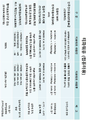
이와 관련하여 도 4에 도시된 본 발명의 일 구성인 전사 타겟이 적용된 타켓 필드 회로부는 USB 타입의 전자파 흡수율 저감 디바이스로 구현되었으며, 이의 테스트 결과는 도 5 및 도 6에 도시된 표와 같이 나타났다.In this regard, the target field circuit unit to which the transfer target, which is one component of the present invention shown in FIG. 4, is applied was implemented as a USB-type electromagnetic wave absorption reduction device, and the test results thereof are shown in the tables shown in FIGS. 5 and 6.
도 5에서 비이타민(스마트폰용)이라고 기재된 것은 스마트폰에 적용된 커넥터 타입의 전자파 흡수율 저감 디바이스에 대한 테스트 결과를 나타낸 것이며, 도 6에서 티파워유(컴퓨터용)이라고 기재된 것은 PC 및 노트북에 적용된 USB 타입의 전자파 흡수율 저감 디바이스에 대한 테스트 결과를 나타낸 것이다.5 shows the test results for the connector-type electromagnetic wave absorption reduction device applied to the smartphone, and the T-power oil (for computers) described in FIG. 6 is a USB type applied to PCs and notebooks. It shows the test results for the electromagnetic absorption rate reduction device of.
테스트 결과는 사용 전과 사용 후를 비교한 것으로부터 알 수 있다시피, 스마트폰에 적용된 커넥터 타입의 전자파 흡수율 저감 디바이스의 경우 전자파 감소율, 스트레스 지수, 인체 온도 변화, 뇌파테스트, 스마트폰 발열, 주관적 피로도에서 감소되거나 개선 효과를 보이고 있다.As can be seen from the comparison of the test results before and after use, in the case of the connector-type electromagnetic wave absorption rate reduction device applied to a smartphone, the electromagnetic wave reduction rate, stress index, body temperature change, brain wave test, smartphone heat, and subjective fatigue. It is decreasing or showing improvement effect.
아울러, PC 및 노트북에 적용된 USB 타입의 전자파 흡수율 저감 디바이스의 경우에도 안구건조증&VDT증후군, 컴퓨터 와이파이 전자파 흡수율(SAR), 컴퓨터 온도시험, 뇌파테스트, 심전도검사, 근전도검사, 인체열, 연산능력 시험, 시력/근육/투통 관련 개선 사항, 황색포도상구균 감소와 관련하여 긍정적인 결과를 보이고 있음을 알 수 있다.In addition, in the case of USB-type electromagnetic wave absorption rate reduction devices applied to PCs and laptops, dry eye syndrome & VDT syndrome, computer Wi-Fi electromagnetic wave absorption rate (SAR), computer temperature test, brain wave test, electrocardiogram test, electromyography, human body heat, computational ability test, It can be seen that there are positive results in relation to improvement in visual acuity/muscle/pain and reduction of Staphylococcus aureus.
이상 첨부된 도면을 참조하여 본 발명의 실시예를 설명하였지만, 상술한 본 발명의 기술적 구성은 본 발명이 속하는 기술 분야의 당업자가 본 발명의 그 기술적 사상이나 필수적 특징을 변경하지 않고서 다른 구체적인 형태로 실시될 수 있다는 것을 이해할 수 있을 것이다. 그러므로 이상에서 기술한 실시 예들은 모든 면에서 예시적인 것이며 한정적인 것이 아닌 것으로서 이해되어야 한다. 아울러, 본 발명의 범위는 상기의 상세한 설명보다는 후술하는 청구범위에 의하여 나타내어진다. 또한, 청구범위의 의미 및 범위 그리고 그 등가 개념으로부터 도출되는 모든 변경 또는 변형된 형태가 본 발명의 범위에 포함되는 것으로 해석되어야 한다.Although the embodiments of the present invention have been described above with reference to the accompanying drawings, the technical configuration of the present invention described above is in other specific forms without changing the technical spirit or essential features of the present invention by those skilled in the art. It will be appreciated that it can be implemented. Therefore, the embodiments described above are illustrative in all respects and should be understood as non-limiting. In addition, the scope of the present invention is indicated by the claims to be described later rather than the detailed description above. In addition, all changes or modifications derived from the meaning and scope of the claims and their equivalent concepts should be interpreted as being included in the scope of the present invention.
S: 소스 물질
T: 전사 타겟
100: 소스 필드 생성부
102: 제1 원통형 코일
104: 제1 나선형 코일
110: 물성 변화부
112: 제2 원통형 코일
114: 제2 나선형 코일
120: 타켓 필드 회로부
122: PCB 기판
130: 프리퀀시 제너레이터S: source material
T: transcription target
100: source field generator
102: first cylindrical coil
104: first spiral coil
110: physical property change part
112: second cylindrical coil
114: second spiral coil
120: target field circuit unit
122: PCB board
130: frequency generator
Claims (5)
상기 제1 원통형 코일에 인접하여 배치된 제2 원통형 코일이 권선되어 내부에 전사 타겟이 수용되고 상기 생성된 소스 필드에 기반하여 상기 전사 타겟의 물성을 변화시키는 물성 변화부; 및
전원이 연결되는 전원 인터페이스가 형성된 PCB 기판과 상기 전원의 입력으로 상기 전사 타겟이 타겟 필드를 형성하도록 제어하는 타겟 필드 회로부를 포함하는 전자파 흡수율 저감 시스템.
A source field generator configured to generate a source field by winding a first cylindrical coil to receive a source material therein and applying a periodic input signal to the first cylindrical coil;
A physical property change unit for receiving a transfer target therein by winding a second cylindrical coil disposed adjacent to the first cylindrical coil, and changing physical properties of the transfer target based on the generated source field; And
An electromagnetic wave absorption rate reduction system comprising: a PCB substrate on which a power supply interface to which power is connected is formed, and a target field circuit configured to control the transfer target to form a target field by an input of the power.
상기 소스 필드 생성부는 상기 제1 원통형 코일의 측면에 배치된 플랫 타입의 제1 나선형 코일을 더 포함하고,
상기 물성 변화부는 상기 제2 원통형 코일의 측면에 배치된 플랫 타입의 제2 나선형 코일을 더 포함하고, 그리고
상기 플랫 타입의 제1, 2 나선형 코일은 상호 연결된 것을 특징으로 하는 전자파 흡수율 저감 시스템.
The method of claim 1,
The source field generator further includes a flat type first spiral coil disposed on a side surface of the first cylindrical coil,
The physical property change unit further includes a flat-type second spiral coil disposed on a side surface of the second cylindrical coil, and
The electromagnetic wave absorption rate reduction system, characterized in that the first and second spiral coils of the flat type are interconnected.
상기 소스 물질은 결정질 물질이고, 상기 전사 타겟은 박막형 금속인 것을 특징으로 하는 전자파 흡수율 저감 시스템.
The method of claim 1,
The source material is a crystalline material, and the transfer target is a thin film type metal.
상기 소스 필드는 종파인 것을 특징으로 하는 전자파 흡수율 저감 시스템.
The method of claim 1,
The electromagnetic wave absorption rate reduction system, wherein the source field is a longitudinal wave.
상기 주기적 입력신호를 생성하기 위한 프리퀀시 제너레이터를 더 포함하고 상기 주기적 입력신호는 상기 소스 물질의 고유 주파수와 매칭되는 주파수인 것을 특징으로 하는 전자파 흡수율 저감 시스템.The method of claim 1,
And a frequency generator for generating the periodic input signal, wherein the periodic input signal is a frequency matched with a natural frequency of the source material.
Priority Applications (4)
| Application Number | Priority Date | Filing Date | Title |
|---|---|---|---|
| KR1020200088160A KR102157469B1 (en) | 2020-07-16 | 2020-07-16 | System for reducing specific absorption rate |
| PCT/KR2021/008419 WO2022014920A1 (en) | 2020-07-16 | 2021-07-02 | System for reducing electromagnetic wave absorption rate |
| CN202180003347.XA CN114208399B (en) | 2020-07-16 | 2021-07-02 | System to reduce electromagnetic wave absorption |
| US17/522,386 US11903178B2 (en) | 2020-07-16 | 2021-11-09 | System for reducing specific absorption rate |
Applications Claiming Priority (1)
| Application Number | Priority Date | Filing Date | Title |
|---|---|---|---|
| KR1020200088160A KR102157469B1 (en) | 2020-07-16 | 2020-07-16 | System for reducing specific absorption rate |
Publications (1)
| Publication Number | Publication Date |
|---|---|
| KR102157469B1 true KR102157469B1 (en) | 2020-09-17 |
Family
ID=72707277
Family Applications (1)
| Application Number | Title | Priority Date | Filing Date |
|---|---|---|---|
| KR1020200088160A Active KR102157469B1 (en) | 2020-07-16 | 2020-07-16 | System for reducing specific absorption rate |
Country Status (4)
| Country | Link |
|---|---|
| US (1) | US11903178B2 (en) |
| KR (1) | KR102157469B1 (en) |
| CN (1) | CN114208399B (en) |
| WO (1) | WO2022014920A1 (en) |
Cited By (1)
| Publication number | Priority date | Publication date | Assignee | Title |
|---|---|---|---|---|
| WO2022014920A1 (en) * | 2020-07-16 | 2022-01-20 | 유앤아이텍(주) | System for reducing electromagnetic wave absorption rate |
Families Citing this family (1)
| Publication number | Priority date | Publication date | Assignee | Title |
|---|---|---|---|---|
| CN116015338B (en) * | 2022-12-16 | 2025-12-30 | 维沃移动通信有限公司 | An electronic device |
Citations (4)
| Publication number | Priority date | Publication date | Assignee | Title |
|---|---|---|---|---|
| KR20010004862A (en) * | 1999-06-30 | 2001-01-15 | 김철 | Device for Absorbing and Removing Electromagnetic Noise |
| KR20040045160A (en) * | 2002-11-22 | 2004-06-01 | 재단법인 충남대학교 산학연교육연구재단 | SAR Measurement System and Method of Electron Wave |
| JP2018181974A (en) * | 2017-04-07 | 2018-11-15 | 富士通株式会社 | Electronic device and electromagnetic wave absorber |
| JP2019102665A (en) * | 2017-12-04 | 2019-06-24 | 国立大学法人北海道大学 | Electromagnetic wave absorber |
Family Cites Families (14)
| Publication number | Priority date | Publication date | Assignee | Title |
|---|---|---|---|---|
| WO2001005020A1 (en) * | 1999-07-13 | 2001-01-18 | Tokyo Electron Limited | Radio frequency power source for generating an inductively coupled plasma |
| JP2005315744A (en) * | 2004-04-28 | 2005-11-10 | Canon Inc | Detection element, detection apparatus, and detection kit including element and reagent |
| KR100751875B1 (en) * | 2006-05-12 | 2007-08-24 | 순천대학교 산학협력단 | Antenna-integrated wireless power supply that receives power energy using radio waves |
| JP4980322B2 (en) * | 2008-09-17 | 2012-07-18 | アルプス電気株式会社 | Multilayer wiring board and manufacturing method thereof |
| US8988066B2 (en) * | 2011-03-02 | 2015-03-24 | Ksr Ip Holdings Llc | Steering position and torque sensor |
| KR20140053644A (en) * | 2012-10-26 | 2014-05-08 | 주식회사 아울테크놀로지 | Method for improving the induced electromotive force by relatively increasing thickness of cu foil in pcb of wireless charger |
| CN103928991B (en) * | 2014-04-23 | 2017-03-29 | 慈溪市源顺光电科技有限公司 | Magnetic resonance wireless electric energy transmission device based on PCB resonance coupling coil structures |
| US10090713B2 (en) * | 2016-09-30 | 2018-10-02 | Intel Corporation | Multiple coils for wireless power |
| US10916969B2 (en) * | 2016-12-08 | 2021-02-09 | At&T Intellectual Property I, L.P. | Method and apparatus for providing power using an inductive coupling |
| US10103777B1 (en) * | 2017-07-05 | 2018-10-16 | At&T Intellectual Property I, L.P. | Method and apparatus for reducing radiation from an external surface of a waveguide structure |
| US11018525B2 (en) * | 2017-12-07 | 2021-05-25 | At&T Intellectual Property 1, L.P. | Methods and apparatus for increasing a transfer of energy in an inductive power supply |
| US10581275B2 (en) * | 2018-03-30 | 2020-03-03 | At&T Intellectual Property I, L.P. | Methods and apparatus for regulating a magnetic flux in an inductive power supply |
| KR20180105628A (en) * | 2018-09-19 | 2018-09-28 | 유앤아이텍(주) | Device for decreasing electromagnetic wave and reducing stress using longitudinal wave |
| KR102157469B1 (en) * | 2020-07-16 | 2020-09-17 | 김창호 | System for reducing specific absorption rate |
-
2020
- 2020-07-16 KR KR1020200088160A patent/KR102157469B1/en active Active
-
2021
- 2021-07-02 WO PCT/KR2021/008419 patent/WO2022014920A1/en not_active Ceased
- 2021-07-02 CN CN202180003347.XA patent/CN114208399B/en active Active
- 2021-11-09 US US17/522,386 patent/US11903178B2/en active Active
Patent Citations (4)
| Publication number | Priority date | Publication date | Assignee | Title |
|---|---|---|---|---|
| KR20010004862A (en) * | 1999-06-30 | 2001-01-15 | 김철 | Device for Absorbing and Removing Electromagnetic Noise |
| KR20040045160A (en) * | 2002-11-22 | 2004-06-01 | 재단법인 충남대학교 산학연교육연구재단 | SAR Measurement System and Method of Electron Wave |
| JP2018181974A (en) * | 2017-04-07 | 2018-11-15 | 富士通株式会社 | Electronic device and electromagnetic wave absorber |
| JP2019102665A (en) * | 2017-12-04 | 2019-06-24 | 国立大学法人北海道大学 | Electromagnetic wave absorber |
Cited By (1)
| Publication number | Priority date | Publication date | Assignee | Title |
|---|---|---|---|---|
| WO2022014920A1 (en) * | 2020-07-16 | 2022-01-20 | 유앤아이텍(주) | System for reducing electromagnetic wave absorption rate |
Also Published As
| Publication number | Publication date |
|---|---|
| US20220117124A1 (en) | 2022-04-14 |
| WO2022014920A1 (en) | 2022-01-20 |
| CN114208399B (en) | 2024-08-09 |
| US11903178B2 (en) | 2024-02-13 |
| CN114208399A (en) | 2022-03-18 |
Similar Documents
| Publication | Publication Date | Title |
|---|---|---|
| Furse et al. | Basic introduction to bioelectromagnetics | |
| Chahat et al. | A compact UWB antenna for on-body applications | |
| Bahrami et al. | Flexible, polarization-diverse UWB antennas for implantable neural recording systems | |
| Tak et al. | Textile antenna with EBG structure for body surface wave enhancement | |
| KR20100072264A (en) | Maximizing power yield from wireless power magnetic resonators | |
| KR102157469B1 (en) | System for reducing specific absorption rate | |
| Fiocchi et al. | SAR exposure from UHF RFID reader in adult, child, pregnant woman, and fetus anatomical models | |
| Sunohara et al. | Evaluation of nonuniform field exposures with coupling factors | |
| Rajagopal et al. | SAR assessment on three layered spherical human head model irradiated by mobile phone antenna | |
| Le-Huu et al. | Efficient compact radiative near-field wireless power transfer to miniature biomedical implants | |
| Vrba et al. | Novel Applicators for Local Microwave Hyperthermia Based on Zeroth‐Order Mode Resonator Metamaterial | |
| Razek | Thermal effects of electromagnetic origin from heating processes to biological disturbances due to field exposure—A review | |
| Nozadze et al. | EM exposure study on an inhomogeneous child model considering hand effect | |
| CN108599391B (en) | A wireless power transmission device based on near-zero permeability metamaterials | |
| Faruque et al. | Evaluation of EM absorption in human head with metamaterial attachment | |
| Ates et al. | Dosimetry analysis of the human head model due to mobile phone usage at GSM-850 frequency band | |
| Cvetković et al. | Electric field distribution and SAR inside a human eye exposed to VR glasses | |
| Gasmelseed et al. | The effects of metamaterial on electromagnetic fields absorption characteristics of human eye tissues | |
| Salama et al. | Wireless power transmission in human tissue for nerve stimulation | |
| Singh et al. | Design and performance analysis of low profile miniaturized MSPAs for body centric wireless communication in ISM band | |
| Hebelka et al. | Koch slot loop antenna for wireless body‐centric communication | |
| Lin | Mechanisms of Electromagnetic Field Coupling into Biological Systems at ELF and RF Frequencies | |
| Bouklachi et al. | HF coils design and shielding for a medical monitoring patch | |
| Tsolis et al. | Design, realisation and evaluation of a liquid hollow torso phantom appropriate for wearable antenna assessment | |
| TWI304595B (en) |
Legal Events
| Date | Code | Title | Description |
|---|---|---|---|
| PA0109 | Patent application |
St.27 status event code: A-0-1-A10-A12-nap-PA0109 |
|
| PA0201 | Request for examination |
St.27 status event code: A-1-2-D10-D11-exm-PA0201 |
|
| A302 | Request for accelerated examination | ||
| PA0302 | Request for accelerated examination |
St.27 status event code: A-1-2-D10-D17-exm-PA0302 St.27 status event code: A-1-2-D10-D16-exm-PA0302 |
|
| E701 | Decision to grant or registration of patent right | ||
| PE0701 | Decision of registration |
St.27 status event code: A-1-2-D10-D22-exm-PE0701 |
|
| GRNT | Written decision to grant | ||
| PR0701 | Registration of establishment |
St.27 status event code: A-2-4-F10-F11-exm-PR0701 |
|
| PR1002 | Payment of registration fee |
St.27 status event code: A-2-2-U10-U11-oth-PR1002 Fee payment year number: 1 |
|
| PG1601 | Publication of registration |
St.27 status event code: A-4-4-Q10-Q13-nap-PG1601 |
|
| R18-X000 | Changes to party contact information recorded |
St.27 status event code: A-5-5-R10-R18-oth-X000 |
|
| P22-X000 | Classification modified |
St.27 status event code: A-4-4-P10-P22-nap-X000 |
|
| PR1001 | Payment of annual fee |
St.27 status event code: A-4-4-U10-U11-oth-PR1001 Fee payment year number: 4 |
|
| R18-X000 | Changes to party contact information recorded |
St.27 status event code: A-5-5-R10-R18-oth-X000 |
|
| PN2301 | Change of applicant |
St.27 status event code: A-5-5-R10-R11-asn-PN2301 |
|
| PN2301 | Change of applicant |
St.27 status event code: A-5-5-R10-R14-asn-PN2301 |
|
| P14-X000 | Amendment of ip right document requested |
St.27 status event code: A-5-5-P10-P14-nap-X000 |
|
| P16-X000 | Ip right document amended |
St.27 status event code: A-5-5-P10-P16-nap-X000 |
|
| Q16-X000 | A copy of ip right certificate issued |
St.27 status event code: A-4-4-Q10-Q16-nap-X000 |
|
| PR1001 | Payment of annual fee |
St.27 status event code: A-4-4-U10-U11-oth-PR1001 Fee payment year number: 5 |
|
| PR1001 | Payment of annual fee |
St.27 status event code: A-4-4-U10-U11-oth-PR1001 Fee payment year number: 6 |
|
| U11 | Full renewal or maintenance fee paid |
Free format text: ST27 STATUS EVENT CODE: A-4-4-U10-U11-OTH-PR1001 (AS PROVIDED BY THE NATIONAL OFFICE) Year of fee payment: 6 |
|
| R18 | Changes to party contact information recorded |
Free format text: ST27 STATUS EVENT CODE: A-5-5-R10-R18-OTH-X000 (AS PROVIDED BY THE NATIONAL OFFICE) |
|
| R18-X000 | Changes to party contact information recorded |
St.27 status event code: A-5-5-R10-R18-oth-X000 |
|
| R18 | Changes to party contact information recorded |
Free format text: ST27 STATUS EVENT CODE: A-5-5-R10-R18-OTH-X000 (AS PROVIDED BY THE NATIONAL OFFICE) |
|
| R18-X000 | Changes to party contact information recorded |
St.27 status event code: A-5-5-R10-R18-oth-X000 |