KR102057990B1 - 블랑켓 일체형 방열회로기판, 이를 포함하는 백라이트 유닛 - Google Patents
블랑켓 일체형 방열회로기판, 이를 포함하는 백라이트 유닛 Download PDFInfo
- Publication number
- KR102057990B1 KR102057990B1 KR1020120109567A KR20120109567A KR102057990B1 KR 102057990 B1 KR102057990 B1 KR 102057990B1 KR 1020120109567 A KR1020120109567 A KR 1020120109567A KR 20120109567 A KR20120109567 A KR 20120109567A KR 102057990 B1 KR102057990 B1 KR 102057990B1
- Authority
- KR
- South Korea
- Prior art keywords
- heat dissipation
- circuit board
- light emitting
- chassis
- delete delete
- Prior art date
- Legal status (The legal status is an assumption and is not a legal conclusion. Google has not performed a legal analysis and makes no representation as to the accuracy of the status listed.)
- Active
Links
- 230000017525 heat dissipation Effects 0.000 claims abstract description 98
- 239000000758 substrate Substances 0.000 claims description 22
- 230000005855 radiation Effects 0.000 claims description 15
- 230000003287 optical effect Effects 0.000 claims description 14
- 238000000034 method Methods 0.000 claims 4
- 238000005476 soldering Methods 0.000 claims 1
- 239000010410 layer Substances 0.000 description 19
- PXHVJJICTQNCMI-UHFFFAOYSA-N Nickel Chemical compound [Ni] PXHVJJICTQNCMI-UHFFFAOYSA-N 0.000 description 12
- RYGMFSIKBFXOCR-UHFFFAOYSA-N Copper Chemical compound [Cu] RYGMFSIKBFXOCR-UHFFFAOYSA-N 0.000 description 7
- 239000004973 liquid crystal related substance Substances 0.000 description 7
- 229910045601 alloy Inorganic materials 0.000 description 6
- 239000000956 alloy Substances 0.000 description 6
- 229910052782 aluminium Inorganic materials 0.000 description 6
- XAGFODPZIPBFFR-UHFFFAOYSA-N aluminium Chemical compound [Al] XAGFODPZIPBFFR-UHFFFAOYSA-N 0.000 description 6
- 229910052802 copper Inorganic materials 0.000 description 6
- 239000010949 copper Substances 0.000 description 6
- 229910052759 nickel Inorganic materials 0.000 description 6
- 239000000463 material Substances 0.000 description 4
- 239000012790 adhesive layer Substances 0.000 description 3
- 238000005452 bending Methods 0.000 description 3
- 239000007769 metal material Substances 0.000 description 3
- 229910052751 metal Inorganic materials 0.000 description 2
- 239000002184 metal Substances 0.000 description 2
- CERQOIWHTDAKMF-UHFFFAOYSA-M Methacrylate Chemical compound CC(=C)C([O-])=O CERQOIWHTDAKMF-UHFFFAOYSA-M 0.000 description 1
- OAICVXFJPJFONN-UHFFFAOYSA-N Phosphorus Chemical compound [P] OAICVXFJPJFONN-UHFFFAOYSA-N 0.000 description 1
- 150000001875 compounds Chemical class 0.000 description 1
- 239000011889 copper foil Substances 0.000 description 1
- 230000008878 coupling Effects 0.000 description 1
- 238000010168 coupling process Methods 0.000 description 1
- 238000005859 coupling reaction Methods 0.000 description 1
- 238000009792 diffusion process Methods 0.000 description 1
- 230000005684 electric field Effects 0.000 description 1
- 239000003822 epoxy resin Substances 0.000 description 1
- 239000004519 grease Substances 0.000 description 1
- 230000001678 irradiating effect Effects 0.000 description 1
- 150000002739 metals Chemical class 0.000 description 1
- 230000004048 modification Effects 0.000 description 1
- 238000012986 modification Methods 0.000 description 1
- 238000000059 patterning Methods 0.000 description 1
- 230000000149 penetrating effect Effects 0.000 description 1
- 229920000647 polyepoxide Polymers 0.000 description 1
- 229920001721 polyimide Polymers 0.000 description 1
- 239000009719 polyimide resin Substances 0.000 description 1
- 230000000191 radiation effect Effects 0.000 description 1
- 229910000679 solder Inorganic materials 0.000 description 1
- 229920003002 synthetic resin Polymers 0.000 description 1
- 239000000057 synthetic resin Substances 0.000 description 1
Images



Classifications
-
- H—ELECTRICITY
- H05—ELECTRIC TECHNIQUES NOT OTHERWISE PROVIDED FOR
- H05K—PRINTED CIRCUITS; CASINGS OR CONSTRUCTIONAL DETAILS OF ELECTRIC APPARATUS; MANUFACTURE OF ASSEMBLAGES OF ELECTRICAL COMPONENTS
- H05K1/00—Printed circuits
- H05K1/02—Details
- H05K1/0201—Thermal arrangements, e.g. for cooling, heating or preventing overheating
- H05K1/0203—Cooling of mounted components
-
- G—PHYSICS
- G02—OPTICS
- G02F—OPTICAL DEVICES OR ARRANGEMENTS FOR THE CONTROL OF LIGHT BY MODIFICATION OF THE OPTICAL PROPERTIES OF THE MEDIA OF THE ELEMENTS INVOLVED THEREIN; NON-LINEAR OPTICS; FREQUENCY-CHANGING OF LIGHT; OPTICAL LOGIC ELEMENTS; OPTICAL ANALOGUE/DIGITAL CONVERTERS
- G02F1/00—Devices or arrangements for the control of the intensity, colour, phase, polarisation or direction of light arriving from an independent light source, e.g. switching, gating or modulating; Non-linear optics
- G02F1/01—Devices or arrangements for the control of the intensity, colour, phase, polarisation or direction of light arriving from an independent light source, e.g. switching, gating or modulating; Non-linear optics for the control of the intensity, phase, polarisation or colour
- G02F1/13—Devices or arrangements for the control of the intensity, colour, phase, polarisation or direction of light arriving from an independent light source, e.g. switching, gating or modulating; Non-linear optics for the control of the intensity, phase, polarisation or colour based on liquid crystals, e.g. single liquid crystal display cells
- G02F1/133—Constructional arrangements; Operation of liquid crystal cells; Circuit arrangements
- G02F1/1333—Constructional arrangements; Manufacturing methods
- G02F1/1335—Structural association of cells with optical devices, e.g. polarisers or reflectors
-
- H—ELECTRICITY
- H05—ELECTRIC TECHNIQUES NOT OTHERWISE PROVIDED FOR
- H05K—PRINTED CIRCUITS; CASINGS OR CONSTRUCTIONAL DETAILS OF ELECTRIC APPARATUS; MANUFACTURE OF ASSEMBLAGES OF ELECTRICAL COMPONENTS
- H05K1/00—Printed circuits
- H05K1/02—Details
- H05K1/11—Printed elements for providing electric connections to or between printed circuits
- H05K1/111—Pads for surface mounting, e.g. lay-out
Landscapes
- Physics & Mathematics (AREA)
- Engineering & Computer Science (AREA)
- Microelectronics & Electronic Packaging (AREA)
- Nonlinear Science (AREA)
- Mathematical Physics (AREA)
- Chemical & Material Sciences (AREA)
- Crystallography & Structural Chemistry (AREA)
- General Physics & Mathematics (AREA)
- Optics & Photonics (AREA)
- Planar Illumination Modules (AREA)
- Liquid Crystal (AREA)
- Arrangement Of Elements, Cooling, Sealing, Or The Like Of Lighting Devices (AREA)
Abstract
Description
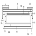
도 2는 본 발명에 따른 블랑켓 일체형 방열회로기판 및 이를 포함하는 백라이트 유닛의 단면도이다.
도 3은 도 2에 도시되어 있는 블랑켓 일체형 방열회로기판의 절곡전 상면도이다.
도 4는 도 3의 방열회로기판의 절곡전 단면도이다.
도 5는 도 4를 적용한 발광모듈을 나타내는 사시도이다.
도 6은 본 발명의 광원의 제1 적용예를 나타내는 사시도이다.
도 7은 본 발명의 광원의 제2 적용예를 나타내는 사시도이다.
도 8은 본 발명의 광원의 제3 적용예를 나타내는 사시도이다.
도 9는 본 발명의 광원의 제4 적용예를 나타내는 사시도이다.
도 10은 본 발명의 광원의 제5 적용예를 나타내는 사시도이다.
샤시 110
발광 소자 170
도광판 180
방열 패턴 132, 133, 134, 135, 136, 137, 138
Claims (15)
- 바닥면과 상기 바닥면으로부터 절곡하는 측면을 가지는 바텀 샤시;
상기 바텀 샤시의 바닥면 상에 배치되는 도광판;
상기 바텀 샤시의 측면 및 바닥면에 부착되며, 상기 도광판의 측면으로 빛을 제공하는 발광 모듈을 포함하며,
상기 발광 모듈은 상기 바텀 샤시의 측면에 부착되는 제1 영역, 그리고 상기 제1 영역과 절곡되어 상기 바텀 샤시의 바닥면에 부착되는 제2 영역을 포함하는 방열회로기판;
상기 제1 영역 위에 배치되는 복수의 발광소자를 포함하고,
상기 제2 영역은 복수의 방열 패턴을 포함하며,
상기 방열 패턴은 상기 제2영역의 상면에 형성되고,
상기 방열 패턴은 상기 방열회로기판의 길이 방향에 대해 사선으로 연장되어 스트라이프 형상을 가지는 백라이트 유닛. - 제1항에 있어서,
상기 방열회로기판은
지지 기판,
상기 지지 기판 위에 형성되어 있는 절연층,
상기 절연층 위에 형성되어 있는 회로 패턴 또는 패드, 그리고
상기 패드를 노출하는 솔더 레지스트를 포함하며,
상기 방열 패턴은 상기 지지 기판에 형성되어 있는 백라이트 유닛. - 제2항에 있어서,
상기 도광판 상에 배치되는 광학 시트를 포함하고,
상기 광학 시트의 면적보다 큰 면적을 갖는 표시 패널이 상기 광학 시트 상에 배치되고,
상기 광학 시트와 상기 표시 패널 사이에 일 부분이 배치되는 지지 부재를 포함하는 백라이트 유닛. - 제3항에 있어서,
상기 표시 패널 상에 배치되는 탑 샤시를 포함하고,
상기 탑 샤시는 상기 바텀 샤시의 측면의 일 영역을 덮도록 배치되는 백라이트 유닛. - 제4항에 있어서,
상기 탑 샤시는 상기 발광 모듈과 수직 방향으로 오버랩되도록 배치되는 백라이트 유닛. - 삭제
- 삭제
- 삭제
- 삭제
- 삭제
- 삭제
- 삭제
- 삭제
- 삭제
- 삭제
Priority Applications (1)
| Application Number | Priority Date | Filing Date | Title |
|---|---|---|---|
| KR1020120109567A KR102057990B1 (ko) | 2012-09-28 | 2012-09-28 | 블랑켓 일체형 방열회로기판, 이를 포함하는 백라이트 유닛 |
Applications Claiming Priority (1)
| Application Number | Priority Date | Filing Date | Title |
|---|---|---|---|
| KR1020120109567A KR102057990B1 (ko) | 2012-09-28 | 2012-09-28 | 블랑켓 일체형 방열회로기판, 이를 포함하는 백라이트 유닛 |
Publications (2)
| Publication Number | Publication Date |
|---|---|
| KR20140042603A KR20140042603A (ko) | 2014-04-07 |
| KR102057990B1 true KR102057990B1 (ko) | 2019-12-20 |
Family
ID=50651742
Family Applications (1)
| Application Number | Title | Priority Date | Filing Date |
|---|---|---|---|
| KR1020120109567A Active KR102057990B1 (ko) | 2012-09-28 | 2012-09-28 | 블랑켓 일체형 방열회로기판, 이를 포함하는 백라이트 유닛 |
Country Status (1)
| Country | Link |
|---|---|
| KR (1) | KR102057990B1 (ko) |
Citations (1)
| Publication number | Priority date | Publication date | Assignee | Title |
|---|---|---|---|---|
| JP2001311940A (ja) * | 2000-05-01 | 2001-11-09 | Heiwa Corp | 遊技機用液晶表示装置 |
-
2012
- 2012-09-28 KR KR1020120109567A patent/KR102057990B1/ko active Active
Patent Citations (1)
| Publication number | Priority date | Publication date | Assignee | Title |
|---|---|---|---|---|
| JP2001311940A (ja) * | 2000-05-01 | 2001-11-09 | Heiwa Corp | 遊技機用液晶表示装置 |
Also Published As
| Publication number | Publication date |
|---|---|
| KR20140042603A (ko) | 2014-04-07 |
Similar Documents
| Publication | Publication Date | Title |
|---|---|---|
| JP5778899B2 (ja) | バックライトアセンブリ | |
| US9052545B2 (en) | Liquid crystal display device | |
| CN102193245B (zh) | 液晶显示装置 | |
| JP4238921B2 (ja) | 照明装置、電気光学装置及び電子機器 | |
| KR20090079568A (ko) | 광원 유닛, 그 제조 방법 및 이를 구비하는 표시 장치 | |
| JP2004349143A (ja) | 面状光源装置及び表示装置 | |
| CN103574400A (zh) | 光源模块及具有该光源模块的背光组件 | |
| US8284349B2 (en) | Backlight unit and liquid crystal display device module including the same | |
| JP5556856B2 (ja) | 面状光源装置および液晶表示装置 | |
| CN102200658B (zh) | 液晶显示装置 | |
| KR101154790B1 (ko) | 블랑켓 일체형 방열회로기판 및 그를 포함하는 샤시 구조물 | |
| KR101887623B1 (ko) | 인쇄회로기판 및 그를 포함하는 백라이트유닛 | |
| KR101283068B1 (ko) | 블랑켓 일체형 방열회로기판, 이을 포함하는 백라이트 유닛 | |
| KR20120080366A (ko) | 발광 모듈, 이의 제조 방법 및 이를 포함하는 표시 장치 | |
| KR101273009B1 (ko) | 블랑켓 일체형 방열회로기판의 제조 방법 및 그에 이용되는 패턴 마스크 | |
| KR102057990B1 (ko) | 블랑켓 일체형 방열회로기판, 이를 포함하는 백라이트 유닛 | |
| KR101283192B1 (ko) | 블랑켓 일체형 방열회로기판을 포함하는 백라이트 유닛 | |
| KR20130018070A (ko) | 발광 모듈 및 이를 구비한 라이트 유닛 | |
| KR20110108831A (ko) | 라이트 유닛 및 이를 구비한 표시 장치 | |
| KR101294505B1 (ko) | 방열회로기판 및 그를 포함하는 샤시 구조물 | |
| KR102070639B1 (ko) | 방열회로기판, 이를 포함하는 백라이트 유닛 | |
| KR101984080B1 (ko) | 백라이트 유닛 | |
| KR101360605B1 (ko) | 블랑켓 일체형 방열회로기판의 제조 방법 및 제조 장치 | |
| KR20110127549A (ko) | 백라이트 유닛 | |
| KR101382847B1 (ko) | 블랑켓 일체형 방열회로기판을 포함하는 샤시 구조물 및 이를 포함하는 백라이트 유닛 |
Legal Events
| Date | Code | Title | Description |
|---|---|---|---|
| PA0109 | Patent application |
Patent event code: PA01091R01D Comment text: Patent Application Patent event date: 20120928 |
|
| PG1501 | Laying open of application | ||
| A201 | Request for examination | ||
| PA0201 | Request for examination |
Patent event code: PA02012R01D Patent event date: 20170925 Comment text: Request for Examination of Application Patent event code: PA02011R01I Patent event date: 20120928 Comment text: Patent Application |
|
| E902 | Notification of reason for refusal | ||
| PE0902 | Notice of grounds for rejection |
Comment text: Notification of reason for refusal Patent event date: 20190304 Patent event code: PE09021S01D |
|
| E701 | Decision to grant or registration of patent right | ||
| PE0701 | Decision of registration |
Patent event code: PE07011S01D Comment text: Decision to Grant Registration Patent event date: 20190916 |
|
| GRNT | Written decision to grant | ||
| PR0701 | Registration of establishment |
Comment text: Registration of Establishment Patent event date: 20191216 Patent event code: PR07011E01D |
|
| PR1002 | Payment of registration fee |
Payment date: 20191217 End annual number: 3 Start annual number: 1 |
|
| PG1601 | Publication of registration | ||
| PR1001 | Payment of annual fee |
Payment date: 20221114 Start annual number: 4 End annual number: 4 |
|
| PR1001 | Payment of annual fee |
Payment date: 20231113 Start annual number: 5 End annual number: 5 |
|
| PR1001 | Payment of annual fee |
Payment date: 20241118 Start annual number: 6 End annual number: 6 |