KR102037688B1 - Display device - Google Patents
Display device Download PDFInfo
- Publication number
- KR102037688B1 KR102037688B1 KR1020130017148A KR20130017148A KR102037688B1 KR 102037688 B1 KR102037688 B1 KR 102037688B1 KR 1020130017148 A KR1020130017148 A KR 1020130017148A KR 20130017148 A KR20130017148 A KR 20130017148A KR 102037688 B1 KR102037688 B1 KR 102037688B1
- Authority
- KR
- South Korea
- Prior art keywords
- data lines
- subpixel
- data
- subpixels
- signal
- Prior art date
- Legal status (The legal status is an assumption and is not a legal conclusion. Google has not performed a legal analysis and makes no representation as to the accuracy of the status listed.)
- Expired - Fee Related
Links
Images


Classifications
-
- G—PHYSICS
- G09—EDUCATION; CRYPTOGRAPHY; DISPLAY; ADVERTISING; SEALS
- G09G—ARRANGEMENTS OR CIRCUITS FOR CONTROL OF INDICATING DEVICES USING STATIC MEANS TO PRESENT VARIABLE INFORMATION
- G09G3/00—Control arrangements or circuits, of interest only in connection with visual indicators other than cathode-ray tubes
- G09G3/20—Control arrangements or circuits, of interest only in connection with visual indicators other than cathode-ray tubes for presentation of an assembly of a number of characters, e.g. a page, by composing the assembly by combination of individual elements arranged in a matrix no fixed position being assigned to or needed to be assigned to the individual characters or partial characters
- G09G3/34—Control arrangements or circuits, of interest only in connection with visual indicators other than cathode-ray tubes for presentation of an assembly of a number of characters, e.g. a page, by composing the assembly by combination of individual elements arranged in a matrix no fixed position being assigned to or needed to be assigned to the individual characters or partial characters by control of light from an independent source
- G09G3/36—Control arrangements or circuits, of interest only in connection with visual indicators other than cathode-ray tubes for presentation of an assembly of a number of characters, e.g. a page, by composing the assembly by combination of individual elements arranged in a matrix no fixed position being assigned to or needed to be assigned to the individual characters or partial characters by control of light from an independent source using liquid crystals
- G09G3/3611—Control of matrices with row and column drivers
- G09G3/3696—Generation of voltages supplied to electrode drivers
-
- G—PHYSICS
- G09—EDUCATION; CRYPTOGRAPHY; DISPLAY; ADVERTISING; SEALS
- G09G—ARRANGEMENTS OR CIRCUITS FOR CONTROL OF INDICATING DEVICES USING STATIC MEANS TO PRESENT VARIABLE INFORMATION
- G09G3/00—Control arrangements or circuits, of interest only in connection with visual indicators other than cathode-ray tubes
- G09G3/20—Control arrangements or circuits, of interest only in connection with visual indicators other than cathode-ray tubes for presentation of an assembly of a number of characters, e.g. a page, by composing the assembly by combination of individual elements arranged in a matrix no fixed position being assigned to or needed to be assigned to the individual characters or partial characters
- G09G3/34—Control arrangements or circuits, of interest only in connection with visual indicators other than cathode-ray tubes for presentation of an assembly of a number of characters, e.g. a page, by composing the assembly by combination of individual elements arranged in a matrix no fixed position being assigned to or needed to be assigned to the individual characters or partial characters by control of light from an independent source
- G09G3/36—Control arrangements or circuits, of interest only in connection with visual indicators other than cathode-ray tubes for presentation of an assembly of a number of characters, e.g. a page, by composing the assembly by combination of individual elements arranged in a matrix no fixed position being assigned to or needed to be assigned to the individual characters or partial characters by control of light from an independent source using liquid crystals
- G09G3/3607—Control arrangements or circuits, of interest only in connection with visual indicators other than cathode-ray tubes for presentation of an assembly of a number of characters, e.g. a page, by composing the assembly by combination of individual elements arranged in a matrix no fixed position being assigned to or needed to be assigned to the individual characters or partial characters by control of light from an independent source using liquid crystals for displaying colours or for displaying grey scales with a specific pixel layout, e.g. using sub-pixels
-
- G—PHYSICS
- G09—EDUCATION; CRYPTOGRAPHY; DISPLAY; ADVERTISING; SEALS
- G09G—ARRANGEMENTS OR CIRCUITS FOR CONTROL OF INDICATING DEVICES USING STATIC MEANS TO PRESENT VARIABLE INFORMATION
- G09G3/00—Control arrangements or circuits, of interest only in connection with visual indicators other than cathode-ray tubes
- G09G3/20—Control arrangements or circuits, of interest only in connection with visual indicators other than cathode-ray tubes for presentation of an assembly of a number of characters, e.g. a page, by composing the assembly by combination of individual elements arranged in a matrix no fixed position being assigned to or needed to be assigned to the individual characters or partial characters
- G09G3/34—Control arrangements or circuits, of interest only in connection with visual indicators other than cathode-ray tubes for presentation of an assembly of a number of characters, e.g. a page, by composing the assembly by combination of individual elements arranged in a matrix no fixed position being assigned to or needed to be assigned to the individual characters or partial characters by control of light from an independent source
- G09G3/36—Control arrangements or circuits, of interest only in connection with visual indicators other than cathode-ray tubes for presentation of an assembly of a number of characters, e.g. a page, by composing the assembly by combination of individual elements arranged in a matrix no fixed position being assigned to or needed to be assigned to the individual characters or partial characters by control of light from an independent source using liquid crystals
- G09G3/3611—Control of matrices with row and column drivers
- G09G3/3614—Control of polarity reversal in general
Landscapes
- Engineering & Computer Science (AREA)
- Chemical & Material Sciences (AREA)
- Crystallography & Structural Chemistry (AREA)
- Physics & Mathematics (AREA)
- Computer Hardware Design (AREA)
- General Physics & Mathematics (AREA)
- Theoretical Computer Science (AREA)
- Control Of Indicators Other Than Cathode Ray Tubes (AREA)
- Liquid Crystal Display Device Control (AREA)
- Liquid Crystal (AREA)
Abstract
표시 장치는: 각각이 제1 방향으로 신장된 복수의 게이트 라인들 및 각각이 제2 방향으로 신장된 복수의 데이터 라인들에 각각 연결된 복수의 서브 픽셀들을 포함하는 표시 패널과, 상기 복수의 게이트 라인들을 구동하는 게이트 드라이버와, 상기 복수의 데이터 라인들로 계조 전압을 제공하는 데이터 드라이버, 및 상기 게이트 드라이버 및 상기 데이터 드라이버를 제어하기 위한 복수의 제어 신호들을 발생하는 타이밍 컨트롤러를 포함한다. 하나의 픽셀은 상기 복수의 서브 픽셀들 중 인접한 짝수 개의 서브 픽셀들을 포함하며, 상기 데이터 라인들 각각은 상기 복수의 서브 픽셀들 중 대응하는 서브 픽셀들의 일측에 각각 연결되고, 상기 데이터 드라이버는 2개의 데이터 라인들마다 번갈아 상기 계조 전압의 극성을 반전시키되, 상기 하나의 픽셀 내 인접한 2 개의 서브 픽셀들로 제공되는 계조 전압들의 극성은 서로 다르다.A display device includes: a display panel including a plurality of gate lines each extending in a first direction and a plurality of subpixels each connected to a plurality of data lines each extending in a second direction, and the plurality of gate lines And a timing controller for generating a plurality of control signals for controlling the gate driver and the data driver. One pixel includes adjacent even subpixels of the plurality of subpixels, each of the data lines being connected to one side of corresponding subpixels of the plurality of subpixels, respectively; The polarity of the gray voltage is alternately inverted for each data line, but the polarities of the gray voltages provided to two adjacent subpixels in the one pixel are different from each other.

Description
본 발명은 표시 장치에 관한 것이다.The present invention relates to a display device.
일반적으로 표시 장치는 영상을 표시하기 위한 표시 패널과 표시 패널을 구동하는 데이터 드라이버 및 게이트 드라이버를 포함한다. 표시 패널은 복수의 게이트 라인, 복수의 데이터 라인 및 복수의 서브 픽셀들을 포함한다. 서브 픽셀 각각은 박막 트랜지스터, 액정 커패시터 및 스토리지 커패시터를 포함한다. 데이터 드라이버는 데이터 라인들에 계조 전압을 출력하고, 게이트 드라이버는 게이트 라인들을 구동하기 위한 게이트 신호를 출력한다.In general, a display device includes a display panel for displaying an image, a data driver and a gate driver for driving the display panel. The display panel includes a plurality of gate lines, a plurality of data lines, and a plurality of sub pixels. Each of the subpixels includes a thin film transistor, a liquid crystal capacitor, and a storage capacitor. The data driver outputs a gray voltage to the data lines, and the gate driver outputs a gate signal for driving the gate lines.
이러한 표시 장치는 표시하고자 하는 게이트 라인에 연결된 박막 트랜지스터의 게이트 전극에 게이트 온 전압을 인가한 후, 표시 영상에 대응하는 데이터 전압을 소스 전극에 인가하여 영상을 표시할 수 있다. 박막 트랜지스터가 턴 온됨에 따라서 액정 커패시터 및 스토리지 커패시터에 인가된 데이터 전압은 박막 트랜지스터가 턴 오프된 후에도 소정 시간 지속되는 것이 바람직하다.Such a display device may display a image by applying a gate-on voltage to a gate electrode of a thin film transistor connected to a gate line to be displayed, and then applying a data voltage corresponding to the display image to a source electrode. As the thin film transistor is turned on, the data voltage applied to the liquid crystal capacitor and the storage capacitor may be maintained for a predetermined time even after the thin film transistor is turned off.
일반적으로 서브 픽셀 내 액정 커패시터에 한쪽 방향의 전기장을 계속해서 인가하면 액정층의 전기적, 물리적인 특성이 나빠지므로 전기장의 방향을 주기적으로 바꾸어줄 필요가 있다. 전기장의 방향을 바꾸기 위해서 한 전극의 전압에 대한 다른 전극의 전압 극성을 반전시키는 방식이 널리 사용되고 있다. 반전 구동을 위해서는 매 프레임마다 서브 픽셀로 인가하는 계조 전압의 극성을 반전시키는 것이 필요하다.In general, if the electric field in one direction is continuously applied to the liquid crystal capacitor in the sub-pixel, the electrical and physical characteristics of the liquid crystal layer deteriorate, and thus the direction of the electric field needs to be periodically changed. In order to change the direction of the electric field, a method of inverting the voltage polarity of another electrode with respect to the voltage of one electrode is widely used. For inversion driving, it is necessary to invert the polarity of the gray voltage applied to the subpixel every frame.
한편, 일반적으로 표시 장치는 레드, 블루 및 그린의 삼원색을 이용하여 색을 표현한다. 그러므로 표시 패널은 레드, 블루 및 그린에 각각 대응하는 서브 픽셀들을 구비한다. 최근에는 표시 영상의 휘도를 증대시키기 위하여 화이트 서브 픽셀을 더 포함하는 기술이 제시되었다. 외부로부터 제공된 레드, 블루 및 그린 영상 신호는 레드, 블루, 그린 및 화이트 데이터 신호로 변환되어서 표시 패널로 제공되야 한다.On the other hand, the display device generally uses three primary colors of red, blue, and green to express colors. Therefore, the display panel has subpixels corresponding to red, blue, and green, respectively. Recently, a technique of further including white subpixels has been proposed to increase luminance of a display image. Red, blue, and green image signals provided from the outside should be converted into red, blue, green, and white data signals and provided to the display panel.
본 발명의 목적은 표시 영상의 품질이 향상된 표시 장치를 제공하는데 있다.An object of the present invention is to provide a display device with improved display image quality.
이와 같은 목적을 달성하기 위한 본 발명의 일 특징에 의하면, 표시 장치는: 각각이 제1 방향으로 신장된 복수의 게이트 라인들 및 각각이 제2 방향으로 신장된 복수의 데이터 라인들에 각각 연결된 복수의 서브 픽셀들을 포함하는 표시 패널과, 상기 복수의 게이트 라인들을 구동하는 게이트 드라이버와, 상기 복수의 데이터 라인들로 계조 전압을 제공하는 데이터 드라이버, 및 상기 게이트 드라이버 및 상기 데이터 드라이버를 제어하기 위한 복수의 제어 신호들을 발생하는 타이밍 컨트롤러를 포함한다. 하나의 픽셀은 상기 복수의 서브 픽셀들 중 인접한 짝수 개의 서브 픽셀들을 포함하며, 상기 데이터 라인들 각각은 상기 복수의 서브 픽셀들 중 대응하는 서브 픽셀들의 일측에 각각 연결되고, 상기 데이터 드라이버는 2개의 데이터 라인들마다 번갈아 상기 계조 전압의 극성을 반전시키되, 상기 하나의 픽셀 내 인접한 2 개의 서브 픽셀들로 제공되는 계조 전압들의 극성은 서로 다르다.According to an aspect of the present invention for achieving the above object, the display device includes: a plurality of gate lines each extending in the first direction and a plurality of data lines respectively connected to the plurality of data lines extending in the second direction A display panel including subpixels of the display panel, a gate driver driving the plurality of gate lines, a data driver providing a gray voltage to the plurality of data lines, and a plurality of controlling the gate driver and the data driver. And a timing controller for generating control signals. One pixel includes adjacent even subpixels of the plurality of subpixels, each of the data lines being connected to one side of corresponding subpixels of the plurality of subpixels, respectively; The polarity of the gray voltage is alternately inverted for each data line, but the polarities of the gray voltages provided to two adjacent subpixels in the one pixel are different from each other.
이 실시예에 있어서, 상기 하나의 픽셀은 제1 타입 픽셀 및 제2 타입 픽셀을 포함하되, 상기 제1 타입 픽셀 및 상기 제2 타입 픽셀 각각은 레드 서브 픽셀, 그린 서브 픽셀, 블루 서브 픽셀 및 화이트 서브 픽셀 중 2개의 서브 픽셀들을 포함한다.In this embodiment, the one pixel includes a first type pixel and a second type pixel, wherein each of the first type pixel and the second type pixel is a red subpixel, a green subpixel, a blue subpixel, and a white. Two subpixels of the subpixels are included.
이 실시예에 있어서, 상기 제1 타입 픽셀은 레드 서브 픽셀 및 그린 서브 픽셀을 포함하고, 상기 제2 타입 픽셀은 블루 서브 픽셀 및 화이트 서브 픽셀을 포함한다.In this embodiment, the first type pixel includes a red sub pixel and a green sub pixel, and the second type pixel includes a blue sub pixel and a white sub pixel.
이 실시예에 있어서, 상기 제1 타입 픽셀 및 상기 제2 타입 픽셀은 상기 제1 방향 및 상기 제2 방향으로 서로 인접하게 배열된다.In this embodiment, the first type pixel and the second type pixel are arranged adjacent to each other in the first direction and the second direction.
이 실시예에 있어서, 상기 데이터 라인들 각각은 상기 복수의 서브 픽셀들 중 대응하는 서브 픽셀들의 좌측에 각각 연결된다.In this embodiment, each of the data lines is connected to a left side of corresponding subpixels of the plurality of subpixels, respectively.
이 실시예에 있어서, 상기 데이터 드라이버는 매 프레임마다 상기 복수의 데이터 라인들 각각을 통해 제공되는 상기 계조 전압의 극성을 반전시킨다.In this embodiment, the data driver inverts the polarity of the gray voltage provided through each of the plurality of data lines every frame.
이 실시예에 있어서, 상기 복수의 데이터 라인들 중 제1 데이터 라인들에는 상기 제1 방향으로 레드 서브 픽셀 및 블루 서브 픽셀이 순차적으로 번갈아 연결되고, 상기 복수의 데이터 라인들 중 제2 데이터 라인들에는 상기 제1 방향으로 그린 서브 픽셀 및 화이트 서브 픽셀이 순차적으로 번갈아 연결되고, 상기 복수의 데이터 라인들 중 제3 데이터 라인들에는 상기 제1 방향으로 블루 서브 픽셀 및 레드 서브 픽셀이 순차적으로 번갈아 연결되고, 상기 복수의 데이터 라인들 중 제4 데이터 라인들에는 상기 제1 방향으로 화이트 서브 픽셀 및 그린 서브 픽셀이 순차적으로 번갈아 연결된다. 상기 제1 내지 제4 데이터 라인들이 상기 제2 방향으로 순차적으로 배열된다.In the present exemplary embodiment, red subpixels and blue subpixels are alternately connected to first data lines of the plurality of data lines in the first direction, and second data lines of the plurality of data lines are alternately connected. Sub greens and white sub pixels drawn in the first direction are alternately connected to each other, and blue sub pixels and red sub pixels are sequentially connected to third data lines of the plurality of data lines in the first direction. The white subpixel and the green subpixel are sequentially connected to fourth data lines of the plurality of data lines in the first direction. The first to fourth data lines are sequentially arranged in the second direction.
이 실시예에 있어서, 상기 타이밍 컨트롤러는, 외부로부터 제공되는 영상 신호에 응답해서 데이터 신호를 상기 데이터 드라이버로 제공하되, 상기 영상 신호가 소정의 영상 패턴일 때 반전 모드 신호를 활성화한다.In this embodiment, the timing controller provides a data signal to the data driver in response to an image signal provided from the outside, and activates an inversion mode signal when the image signal is a predetermined image pattern.
이 실시예에 있어서, 상기 데이터 드라이버는, 상기 데이터 신호를 수신하고, 상기 반전 모드 신호에 응답해서 상기 복수의 데이터 라인들로 제공되는 상기 계조 전압의 극성을 설정한다.In this embodiment, the data driver receives the data signal and sets the polarity of the gray voltage provided to the plurality of data lines in response to the inversion mode signal.
이 실시예에 있어서, 상기 데이터 드라이버는, 상기 반전 모드 신호가 비활성 상태일 때 상기 2개의 데이터 라인마다 번갈아 상기 계조 전압의 극성을 반전시키되, 상기 하나의 픽셀 내 상기 2 개의 서브 픽셀들로 제공되는 계조 전압들의 극성 서로 다르도록 상기 계조 전압의 극성을 설정한다.In this embodiment, the data driver inverts the polarity of the gray voltage alternately every two data lines when the inversion mode signal is inactive, provided to the two subpixels in the one pixel. Polarities of the gray voltages are set to be different from each other.
이 실시예에 있어서, 상기 데이터 드라이버는, 상기 반전 모드 신호가 활성 상태일 때 매 데이터 라인마다 번갈아 상기 계조 전압의 극성을 반전시킨다.In this embodiment, the data driver inverts the polarity of the gray voltage alternately every data line when the inversion mode signal is active.
이 실시예에 있어서, 상기 데이터 드라이버는, 매 프레임마다 상기 복수의 데이터 라인들 각각을 통해 제공되는 상기 계조 전압의 극성을 반전시킨다.In this embodiment, the data driver inverts the polarity of the gray voltage provided through each of the plurality of data lines every frame.
이 실시예에 있어서, 상기 타이밍 컨트롤러는, 상기 영상 신호를 상기 레드 서브 픽셀, 상기 그린 서브 픽셀, 상기 블루 서브 픽셀 및 상기 화이트 서브 픽셀에 대응하는 상기 데이터 신호로 변환하는 펜타일 변환부 및, 상기 영상 신호가 상기 소정의 영상 패턴일 때 상기 반전 모드 신호를 활성화하는 반전 모드 선택기를 포함한다.The timing controller may include a pentile converter configured to convert the image signal into the data signal corresponding to the red subpixel, the green subpixel, the blue subpixel, and the white subpixel. And an inversion mode selector for activating the inversion mode signal when the image signal is the predetermined image pattern.
이 실시예에 있어서, 상기 소정의 영상 패턴은, 상기 그린 서브 픽셀 및 상기 블루 서브 픽셀을 온 시키고 그리고 상기 레드 서브 픽셀 및 상기 화이트 서브 픽셀을 오프시키는 영상 패턴이다.In this embodiment, the predetermined image pattern is an image pattern that turns on the green subpixel and the blue subpixel and turns off the red subpixel and the white subpixel.
이 실시예에 있어서, 상기 타이밍 컨트롤러는, 상기 영상 신호가 상기 소정의 영상 패턴인 것을 감지했을 때 다음 프레임의 시작 시점에 반전 모드 신호를 활성화한다.In this embodiment, the timing controller activates the inversion mode signal at the start of the next frame when it detects that the video signal is the predetermined video pattern.
이와 같은 구성을 갖는 본 발명의 표시 장치에서 하나의 픽셀은 짝수 개의 서브 픽셀들을 포함하며, 2개의 데이터 라인들마다 번갈아 계조 전압의 극성을 반전시키되, 하나의 픽셀 내 인접한 2 개의 서브 픽셀들로 제공되는 계조 전압들의 극성이 서로 다르도록 데이터 라인들을 구동할 수 있다. 그러므로 영상의 품질이 저하되는 것을 방지할 수 있고, 소비 전력을 감소시킬 수 있다.In the display device according to the exemplary embodiment of the present invention, one pixel includes an even number of subpixels, and alternately inverts the polarity of the gray voltage every two data lines, and provides two adjacent subpixels in one pixel. The data lines may be driven to have different polarities of the gray voltages. Therefore, deterioration of the image quality can be prevented, and power consumption can be reduced.
또한, 크로스토크를 유발하는 소정의 워스트 패턴의 영상 신호가 외부로부터 입력될 때 반전 모드를 변경함으로써 크로스토크를 방지할 수 있다.In addition, crosstalk can be prevented by changing the inversion mode when a video signal having a predetermined worst pattern that causes crosstalk is input from the outside.
도 1은 본 발명의 실시예에 따른 표시 장치의 회로 구성을 보여주는 도면이다.
도 2는 도 1에 도시된 표시 패널 내 픽셀들의 배치 예를 보여주는 도면이다.
도 3은 도 1에 도시된 표시 패널의 다른 실시예에 따른 픽셀 배열을 보여주는 도면이다.
도 4는 도 3에 도시된 표시 패널 내 각 픽셀로 제공되는 계조 전압의 킥백 전압을 예시적으로 보여주는 도면이다.
도 5 및 도 6은 도 4에 도시된 표시 패널의 일부를 보여주는 도면이다.
도 7은 도 1에 도시된 표시 패널의 다른 실시예에 따른 픽셀 배열을 보여주는 도면이다.
도 8은 도 7에 도시된 표시 패널의 일부를 보여주는 도면이다.
도 9는 도 8에 도시된 표시 패널의 데이터 라인들로 제공되는 계조 전압을 보여주는 도면이다.
도 10은 도 7에 도시된 표시 패널의 일부를 보여주는 도면이다.
도 11은 도 10에 도시된 표시 패널의 데이터 라인들로 제공되는 계조 전압을 보여주는 도면이다.
도 12는 도 3에 도시된 표시 패널의 일부를 보여주는 도면이다.
도 13은 도 12에 도시된 표시 패널의 데이터 라인들로 제공되는 계조 전압을 보여주는 도면이다.
도 14는 본 발명의 다른 실시예에 따른 표시 장치를 보여주는 도면이다.
도 15는 도 14에 도시된 타이밍 컨트롤러의 구체적인 구성 예를 보여주는 블록도이다.
도 16은 도 14에 도시된 타이밍 컨트롤러로부터 출력되는 반전 모드 신호가 로우 레벨에서 하이 레벨로 변경될 때 표시 패널을 구동하는 계조 전압의 변화를 보여주는 도면이다.
도 17은 도 15에 도시된 반전 모드 선택기로부터 출력되는 반전 모드 신호의 일 예를 보여주는 타이밍도이다.1 illustrates a circuit configuration of a display device according to an exemplary embodiment of the present invention.
FIG. 2 is a diagram illustrating an arrangement example of pixels in the display panel illustrated in FIG. 1.
3 is a diagram illustrating a pixel array according to another exemplary embodiment of the display panel shown in FIG. 1.
4 is a diagram illustrating a kickback voltage of a gray voltage provided to each pixel in the display panel illustrated in FIG. 3.
5 and 6 illustrate a portion of the display panel illustrated in FIG. 4.
FIG. 7 is a diagram illustrating a pixel array according to another exemplary embodiment of the display panel illustrated in FIG. 1.
FIG. 8 is a diagram illustrating a part of the display panel illustrated in FIG. 7.
FIG. 9 is a diagram illustrating a gray voltage provided to data lines of the display panel illustrated in FIG. 8.
FIG. 10 is a view illustrating a portion of the display panel illustrated in FIG. 7.
FIG. 11 is a diagram illustrating a gray voltage provided to data lines of the display panel illustrated in FIG. 10.
FIG. 12 is a view illustrating a portion of the display panel illustrated in FIG. 3.
FIG. 13 is a diagram illustrating a gray voltage provided to data lines of the display panel illustrated in FIG. 12.
14 is a diagram illustrating a display device according to another exemplary embodiment of the present invention.
FIG. 15 is a block diagram illustrating a specific configuration example of the timing controller illustrated in FIG. 14.
FIG. 16 is a view illustrating a change in a gray voltage driving the display panel when the inversion mode signal output from the timing controller shown in FIG. 14 is changed from a low level to a high level.
17 is a timing diagram illustrating an example of an inversion mode signal output from the inversion mode selector illustrated in FIG. 15.
이하 본 발명의 실시예를 첨부된 도면들을 참조하여 상세히 설명한다.Hereinafter, embodiments of the present invention will be described in detail with reference to the accompanying drawings.
도 1은 본 발명의 실시예에 따른 표시 장치의 회로 구성을 보여주는 도면이다.1 illustrates a circuit configuration of a display device according to an exemplary embodiment of the present invention.
도 1을 참조하면, 표시 장치(100)는 표시 패널(110), 타이밍 컨트롤러(120), 게이트 드라이버(130) 및 데이터 드라이버(140)를 포함한다.Referring to FIG. 1, the
표시 패널(110)은 제1 방향(X1)으로 신장된 복수의 데이터 라인들(DL1-DLm) 및 데이터 라인들(DL1-DLm)에 교차하여 제2 방향(X2)으로 신장된 복수의 게이트 라인들(GL1-GLn) 그리고 그들의 교차 영역에 행렬의 형태로 배열된 복수의 서브 픽셀들(SPX)을 포함한다(단, n 및 m 각각은 0이 아닌 자연수). 복수의 데이터 라인들(DL1-DLm)과 복수의 게이트 라인들(GL1-GLn)은 서로 절연되어 있다.The
각 서브 픽셀(SPX)은 대응하는 데이터 라인 및 게이트 라인에 연결된 스위칭 트랜지스터(TR)와 이에 연결된 액정 커패시터(crystal capacitor, CLC) 및 스토리지 커패시터(storage capacitor, CST)를 포함한다.Each sub-pixel SPX includes a switching transistor TR connected to a corresponding data line and a gate line, a crystal capacitor CLC, and a storage capacitor CST connected thereto.
복수의 서브 픽셀들(SPX)은 동일한 구조로 이루어진다. 따라서, 하나의 서브 픽셀의 구성을 설명함으로써, 서브 픽셀들(SPX) 각각에 대한 설명은 생략한다. 서브 픽셀(SPX)의 스위칭 트랜지스터(TR)는 복수 게이트 라인들(GL1~GLn) 중 제1 게이트 라인(GL1)에 연결된 게이트 전극, 복수의 데이터 라인들(DL1~DLm) 중 제1 데이터 라인(DL1)에 연결된 소스 전극 및 액정 커패시터(CLC)와 스토리지 커패시터(CST)에 연결된 드레인 전극을 구비한다. 액정 커패시터(CLC)와 스토리지 커패시터(CST) 각각의 일단은 스위칭 트랜지스터(TR)의 드레인 전극에 병렬 연결된다. 액정 커패시터(CLC)와 스토리지 커패시터(CST) 각각의 타단은 공통 전압과 연결될 수 있다. 스위칭 트랜지스터(TR)는 박막 트랜지스터(thin film transistor)로 구성될 수 있다.The plurality of subpixels SPX have the same structure. Therefore, the description of each subpixel SPX is omitted by describing the configuration of one subpixel. The switching transistor TR of the subpixel SPX includes a gate electrode connected to the first gate line GL1 among the plurality of gate lines GL1 to GLn, and a first data line among the plurality of data lines DL1 to DLm. And a drain electrode connected to the liquid crystal capacitor CLC and the storage capacitor CST. One end of each of the liquid crystal capacitor CLC and the storage capacitor CST is connected in parallel to the drain electrode of the switching transistor TR. The other end of each of the liquid crystal capacitor CLC and the storage capacitor CST may be connected to a common voltage. The switching transistor TR may be configured as a thin film transistor.
타이밍 컨트롤러(120)는 외부로부터 영상 신호(RGB) 및 이의 표시를 제어하기 위한 제어 신호들(CTRL) 예를 들면, 수직 동기 신호, 수평 동기 신호, 메인 클럭 신호 및 데이터 인에이블 신호 등을 제공받는다. 타이밍 컨트롤러(120)는 제어 신호들(CTRL)에 기초하여 영상 신호(RGB)를 표시 패널(110)의 동작 조건에 맞게 처리한 데이터 신호(DATA) 및 제1 제어 신호(CONT1)를 데이터 드라이버(140)로 제공하고, 제2 제어 신호(CONT2)를 게이트 드라이버(130)로 제공한다. 제1 제어 신호(CONT1)는 수평 동기 시작 신호, 클럭 신호 및 라인 래치 신호를 포함할 수 있고, 제2 제어 신호(CONT2)는 수직 동기 시작 신호, 출력 인에이블 신호 및 게이트 펄스 신호를 포함할 수 있다.The
데이터 드라이버(140)는 타이밍 컨트롤러(120)로부터의 데이터 신호(DATA) 및 제1 제어 신호(CONT1)에 따라서 데이터 라인들(DL1-DLm) 각각을 구동하기 위한 계조 전압들을 출력한다.The
게이트 드라이버(130)는 타이밍 컨트롤러(120)로부터의 제2 제어 신호(CONT2)과 전압 발생기(130)로부터의 게이트 온 전압(VON) 및 게이트 오프 전압(VOFF)에 응답해서 게이트 라인들(GL1-GLn)을 구동한다. 게이트 드라이버(130)는 하나 또는 둘 이상의 게이트 구동 IC(Integrated circuit)를 포함할 수 있다.The
게이트 드라이버(130)는 게이트 구동 IC뿐만 아니라 비정질-실리콘 박막 트랜지스터(amorphous Silicon Thin Film Transistor a-Si TFT)를 이용한 ASG(Amorphous silicon gate), 산화물 반도체, 결정질 반도체, 다결정 반도체 등을 이용한 회로로 구현될 수도 있다. The
하나의 게이트 라인에 게이트 온 전압(VON)이 인가된 동안 이에 연결된 한 행의 스위칭 트랜지스터가 턴 온되고, 이때 데이터 드라이버(140)는 데이터 신호(DATA)에 대응하는 계조 전압들을 데이터 라인들(DL1-DLm)로 제공한다. 데이터 라인들(DL1-DLm)에 공급된 계조 전압들은 턴 온된 스위칭 트랜지스터를 통해 해당 픽셀에 인가된다. 여기서, 한 행의 스위칭 트랜지스터가 턴 온 되어 있는 기간 즉, 출력 인에이블 신호 및 게이트 펄스 신호의 한 주기를 ‘1 수평 주기(horizontal period)' 또는 ‘1H'라고 한다.While a gate-on voltage VON is applied to one gate line, a row of switching transistors connected thereto is turned on. At this time, the
도 2는 도 1에 도시된 표시 패널 내 픽셀들의 배치 예를 보여주는 도면이다.FIG. 2 is a diagram illustrating an arrangement example of pixels in the display panel illustrated in FIG. 1.
도 2를 참조하면, 표시 패널(110a)은 제1 타입 픽셀(PX1) 및 제2 타입 픽셀(PX2)을 포함한다. 제1 타입 픽셀(PX1) 및 제2 타입 픽셀(PX2) 각각은 짝수 개의 서브 픽셀들을 포함한다. 이 실시예에서, 제1 타입 픽셀(PX1) 및 제2 타입 픽셀(PX2) 각각은 2 개의 서브 픽셀들을 포함한다. 일 예로, 제1 타입 픽셀(PX1)은 레드 서브 픽셀 및 그린 서브 픽셀을 포함하고, 제2 타입 픽셀(PX2)은 블루 서브 픽셀 및 화이트 서브 픽셀을 포함한다.Referring to FIG. 2, the
앞서 도 1에서 설명한 바와 같이, 서브 픽셀들(SPX) 각각은 스위칭 트랜지스터(TR), 액커패시터(CLC) 및 스토리지 커패시터(CST)를 포함한다. 도 2에서는 서브 픽셀들 각각에 포함된 스위칭 트랜지스터와 액정 커패시터만을 도시하였다. 스위칭 트랜지스터들 각각은 대응하는 데이터 라인과 대응하는 게이트 라인에 연결된다. 제1 타입 픽셀들(PX1) 및 제2 타입 픽셀들(PX2)은 게이트 라인들(GL1-GLn)의 신장 방향인 제1 방향(X1)으로 순차적으로 번갈아 배열된다. 마찬가지로 제1 타입 픽셀들(PX1) 및 제2 타입 픽셀들(PX2)은 데이터 라인들(DL1-DLn)의 신장 방향인 제2 방향(X2)으로 순차적으로 번갈아 배열된다.As described above with reference to FIG. 1, each of the sub pixels SPX includes a switching transistor TR, an capacitor CLC, and a storage capacitor CST. 2 illustrates only a switching transistor and a liquid crystal capacitor included in each of the subpixels. Each of the switching transistors is connected to a corresponding data line and a corresponding gate line. The first type pixels PX1 and the second type pixels PX2 are alternately arranged in the first direction X1, which is an extension direction of the gate lines GL1 -GLn. Similarly, the first type pixels PX1 and the second type pixels PX2 are alternately arranged in the second direction X2, which is an extension direction of the data lines DL1 -DLn.
또한 레드, 그린, 블루 및 화이트 서브 픽셀들은 2 행 단위로 좌측 및 우측 인접 데이터 라인들과 번갈아 연결된 지그재그 연결 구조이다. 즉, g(g는 양의 정수)번째 게이트 라인들(GLg) 및 g+1번째 게이트 라인들(GLg+1)과 연결된 서브 픽셀들은 왼쪽 데이터 라인과 연결되고, g+2번째 게이트 라인들(GLg+2) 및 g+3번째 게이트 라인들(GLg+3)과 연결된 서브 픽셀들은 오른쪽 데이터 라인과 연결된다.In addition, the red, green, blue, and white subpixels have a zigzag connection structure alternately connected to the left and right adjacent data lines in units of two rows. That is, the subpixels connected to the g (g is a positive integer) th gate lines GLg and the g + 1 th gate lines GLg + 1 are connected to the left data line, and the g + 2 th gate lines ( The subpixels connected to GLg + 2) and the g + 3th gate lines GLg + 3 are connected to the right data line.
도 2에서 레드 서브 픽셀은 R, 그린 서브 픽셀은 G, 블루 서브 픽셀은 B 그리고 화이트 서브 픽셀은 W로 표기한다. 또한 레드, 그린, 블루 및 화이트 서브 픽셀들 중 좌측 데이터 라인과 연결되고, i(i는 양의 정수) 번째 프레임에서 정극성(+)으로 구동되는 서브 픽셀은 Ra, Ga, Ca 및 Wa로 표기된다. 레드, 그린, 블루 및 화이트 서브 픽셀들 중 좌측 데이터 라인과 연결되고, i(i는 양의 정수) 번째 프레임에서 음극성(-)으로 구동되는 서브 픽셀은 Rb, Gb, Cb 및 Wb로 표기된다. 레드, 그린, 블루 및 화이트 서브 픽셀들 중 우측 데이터 라인과 연결되어 있으며, i 번째 프레임에서 정극성(+)으로 구동되는 서브 픽셀은 Rc, Gc, Cc 및 Wc로 표기된다. 레드, 그린, 블루 및 화이트 서브 픽셀들 중 우측 데이터 라인과 연결되어 있으며, i 번째 프레임에서 음극성(-)으로 구동되는 서브 픽셀은 Rd, Gd, Cd 및 Wd로 표기된다.In FIG. 2, the red subpixel is denoted by R, the green subpixel is G, the blue subpixel is B, and the white subpixel is denoted by W. Subpixels connected to the left data line of the red, green, blue, and white subpixels and driven positively in the i (i is a positive integer) frame are denoted by Ra, Ga, Ca, and Wa. do. Subpixels connected to the left data line of the red, green, blue and white subpixels and driven negatively in the i (i is a positive integer) th frame are denoted as Rb, Gb, Cb and Wb. . Subpixels connected to the right data line among the red, green, blue, and white subpixels and driven positively in the i-th frame are denoted as Rc, Gc, Cc, and Wc. The subpixels connected to the right data line among the red, green, blue, and white subpixels and driven negatively in the i-th frame are denoted as Rd, Gd, Cd, and Wd.
예컨대, 좌측에 배열된 데이터 라인과 연결되고, i 번째 프레임에서 정극성(+)으로 구동되는 제1 타입 픽셀(PX1) 내 레드 서브 픽셀은 Ra로 표기한다. 좌측에 배열된 데이터 라인과 연결되고, i 번째 프레임에서 정극성(+)으로 구동되는 제1 타입 픽셀(PX1) 내 그린 서브 픽셀은 Gb로 표기한다.For example, the red subpixel in the first type pixel PX1 connected to the data lines arranged on the left side and driven with positive polarity (+) in the i-th frame is denoted by Ra. The green sub-pixel in the first type pixel PX1 connected to the data lines arranged on the left and driven with positive polarity (+) in the i-th frame is denoted by Gb.
이 예에서, 첫 번째 게이트 라인(GL1)과 연결된 서브 픽셀들은, 제1 방향(X1)으로, Ra, Gb, Ba, Wb, Ra, Gb, Ba, Wb, ... 순이다. 두 번째 게이트 라인(GL2)과 연결된 서브 픽셀들은, 제1 방향(D1)으로, Bb, Wa, Rb, Ga, Bb, Wa, Rb, Ga, ... 순이다.In this example, the subpixels connected to the first gate line GL1 are Ra, Gb, Ba, Wb, Ra, Gb, Ba, Wb, ... in the first direction X1. Sub-pixels connected to the second gate line GL2 are in the order of Bb, Wa, Rb, Ga, Bb, Wa, Rb, Ga, ... in the first direction D1.
또한 이 예에서, 첫 번째 데이터 라인(DL1)과 연결된 서브 픽셀들은, 제2 방향(X2)으로 Ra, Bb, Rc, Bd, Ra, Bb, Rc, Bd, ... 순이다. 두 번째 데이터 라인(DL2)과 연결된 서브 픽셀들은, 제2 방향(X2)으로 Gb, Wa, Gd, Wc, Gb, Wa, Gd, Wc, ... 순이다. Also in this example, the subpixels connected to the first data line DL1 are Ra, Bb, Rc, Bd, Ra, Bb, Rc, Bd, ... in the second direction X2. The subpixels connected to the second data line DL2 are in the order of Gb, Wa, Gd, Wc, Gb, Wa, Gd, Wc, ... in the second direction X2.
표시 패널(110a) 내 서브 픽셀들의 배열은 도 2에 한정되지 않고 다양하게 변경될 수 있다.The arrangement of the subpixels in the
도 2에 도시된 표시 패널(110a) 내 각 서브 픽셀로 제공되는 계조 전압의 극성은 i번째 프레임의 극성을 나타낸 것으로 i+1번째 프레임에서 각 서브 픽셀로 제공되는 데이터의 극성은 반전된다.The polarity of the gray voltage provided to each sub-pixel in the
도 2에 도시된 표시 패널(110a)의 서브 픽셀 배열 방식은 한 프레임 동안 다양한 극성의 계조 전압들을 표시할 수 있다. 즉, Ra, Rb, Rc, Rd, Ga, Gb, Gc, Gd, Ba, Bb, Bc, Bd, Da, Db, Dc 및 Dd의 서브 픽셀들이 한 프레임 내에 모두 포함되므로 플리커(flicker)가 감소된다.The subpixel arrangement of the
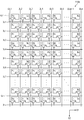
도 3은 도 1에 도시된 표시 패널의 다른 실시예에 따른 픽셀 배열을 보여주는 도면이다.3 is a diagram illustrating a pixel array according to another exemplary embodiment of the display panel shown in FIG. 1.
도 3을 참조하면, 표시 패널(110b)은 도 2에 도시된 표시 패널(110a)과 마찬가지로 제1 타입 픽셀(PX1) 및 제2 타입 픽셀(PX2)을 포함한다. 제1 타입 픽셀(PX1) 및 제2 타입 픽셀(PX2) 각각은 짝수 개의 서브 픽셀들을 포함한다. 이 실시예에서, 제1 타입 픽셀(PX1) 및 제2 타입 픽셀(PX2) 각각은 2 개의 서브 픽셀들을 포함한다. 일 예로, 제1 타입 픽셀(PX1)은 레드 서브 픽셀(R) 및 그린 서브 픽셀(G)을 포함하고, 제2 타입 픽셀(PX2)은 블루 서브 픽셀(B) 및 화이트 서브 픽셀(W)을 포함한다. 또한, 표시 패널(110b) 내 레드 서브 픽셀(R), 그린 서브 픽셀(G), 블루 서브 픽셀(B) 및 화이트 서브 픽셀(W)의 배열 순서는 도 2에 도시된 표시 패널(110a)의 그것들과 동일하다.Referring to FIG. 3, the
다만, 표시 패널(110b) 내 레드 서브 픽셀(R), 그린 서브 픽셀(G), 블루 서브 픽셀(B) 및 화이트 서브 픽셀(W)과 데이터 라인들(DL1-DLm)의 연결 관계는 도 2에 도시된 표시 패널(110a)과 상이하다. However, the connection relationship between the red subpixel R, the green subpixel G, the blue subpixel B, and the white subpixel W and the data lines DL1 -DLm in the
즉, 레드, 그린, 블루 및 화이트 서브 픽셀들은 1+2 행 단위로 좌측 및 우측 인접 데이터 라인들과 번갈아 연결된 지그재그 연결 구조이다. 즉, 1번째 게이트 라인(GL1)과 연결된 서브 픽셀들은 왼쪽 데이터 라인과 연결되고, 이후 g+1(g는 양의 정수)번째 게이트 라인들(GLg+1) 및 g+2번째 게이트 라인들(GLg+2)과 연결된 서브 픽셀들은 오른쪽 데이터 라인과 연결되고, g+3번째 게이트 라인들(GLg+3) 및 g+4번째 게이트 라인들(GLg+4)과 연결된 서브 픽셀들은 왼쪽 데이터 라인과 연결된다.That is, the red, green, blue, and white subpixels have a zigzag connection structure alternately connected to left and right adjacent data lines in units of 1 + 2 rows. That is, the subpixels connected to the first gate line GL1 are connected to the left data line, and then g + 1 (g is a positive integer) gate lines GLg + 1 and g + 2 gate lines ( The subpixels connected to GLg + 2 are connected to the right data line, and the subpixels connected to the g + 3th gate lines GLg + 3 and the g + 4th gate lines GLg + 4 are connected to the left data line. Connected.
도 3에 도시된 표시 패널(110b)은 컬럼 인버전 방식으로 구동된다. 컬럼 인버전 방식은 동일한 데이터 라인에 인가되는 계조 전압의 극성은 동일하고 이웃한 데이터 라인들로 제공되는 계조 전압들의 전극들이 공통 전압(VCOM)을 기준으로 상보적이다.The
이러한 서브 픽셀들과 데이터 라인들의 연결에 의하면, 데이터 드라이버(140)에 의해서 데이터 라인들이 컬럼 인버전 방식으로 구동하더라도 화면에 나타나는 반전 즉, 겉보기 반전(apparent inversion)은 도트 인버전(dot inversion)과 동일하다. 즉, 인접한 서브 픽셀들로 제공되는 계조 전압들이 서로 상보적 극성을 갖는다. 겉보기 반전이 도트 인버전이 되면 계조 전압이 정극성 일 때와 부극성 일 때의 킥백(kick-back) 전압으로 인해서 나타나는 휘도의 차가 분산되므로 세로줄 플리커가 감소한다.According to the connection of the subpixels and the data lines, the inversion that appears on the screen, that is, the apparent inversion, may be caused by the dot inversion and the inversion even though the data lines are driven in the column inversion method by the
도 2에 도시된 표시 패널(110a)도 도트 인버전 방식으로 구동되나, 매 수평 라인마다 즉, 1 수평 주기마다 데이터 라인을 통해 제공되는 계조 전압의 극성을 반전시켜야 하므로 전력 소모가 많다. 그러나, 도 3에 도시된 표시 패널(110b)은 컬럼 인버전 방식으로 구동되므로 전력 소모를 감소시킬 수 있다.Although the
도 4는 도 3에 도시된 표시 패널 내 각 픽셀로 제공되는 계조 전압의 킥백 전압을 예시적으로 보여주는 도면이다.4 is a diagram illustrating a kickback voltage of a gray voltage provided to each pixel in the display panel illustrated in FIG. 3.
도 3 및 도 4를 참조하면, g번째 게이트 라인(GLg)으로 인가되는 신호는 게이트 온 전압(VON)과 게이트 오프 전압(VOFF) 사이를 스윙한다. 게이트 라인(GLg)으로 인가되는 신호는 서브 픽셀 내 스위칭 트랜지스터의 게이트 단자로 제공되고, 이 때 계조 전압(Vsig)이 데이터 라인을 통해 스위칭 트랜지스터의 소스 단자로 제공된다. 또한 계조 전압(Vsig)은 매 프레임마다 공통 전압(VCOM)을 기준으로 정극성에서 음극성으로 또는 음극성에서 정극성으로 반전된다. 이상적인 경우, 공통 전압(VCOM)과 데이터 라인을 통해 제공되는 정극성(+)의 계조 전압(Vsig)의 차(H1)는 공통 전압(VCOM)과 부극성(-)의 계조 전압(Vsig)의 차(L1)와 같다(H1=L1).3 and 4, the signal applied to the g-th gate line GLg swings between the gate on voltage VON and the gate off voltage VOFF. The signal applied to the gate line GLg is provided to the gate terminal of the switching transistor in the sub pixel, and the gray voltage Vsig is provided to the source terminal of the switching transistor through the data line. The gray voltage Vsig is inverted from positive to negative or from negative to positive with respect to the common voltage VCOM every frame. In an ideal case, the difference H1 between the common voltage VCOM and the positive gray voltage Vsig provided through the data line is the difference between the common voltage VCOM and the gray voltage Vsig of the negative polarity V-sig. It is the same as the difference L1 (H1 = L1).
그러나, 표시 패널(110b)의 제조 공정의 문제로 인해 스위칭 트랜지스터의 게이트 전극과 드레인 전극 사이에 존재하는 기생 커패시턴스(Cgd) 때문에 액정 커패시터 및 스토리지 커패시터에 인가된 실제 계조 전압(Vsig)에 왜곡이 생길 수 있다. 즉, 데이터 드라이버(140)로부터 출력된 계조 전압보다 액정 커패시터 및 스토리지 커패시터에 인가된 실제 계조 전압(Vsig)의 전압 레벨이 더 낮아진다. 이와 같이 왜곡된 전압을 킥백(kickback) 전압(ΔV)이라 한다. 정극성(+)의 계조 전압(Vsig)에 대한 킥백 전압을 ΔVPOS라 하고, 음극성(-)의 계조 전압(Vsig)에 대한 킥백 전압을 ΔVNEG라 할 때, 킥백 전압들(ΔVPOS, ΔVNEG)에 의해서 공통 전압(VCOM)과 정극성(+)의 계조 전압(Vsig)의 차(H2)는 공통 전압(VCOM)과 부극성(-)의 계조 전압(Vsig)의 차(L2)는 서로 달라진다(H2<L2).However, the parasitic capacitance Cgd existing between the gate electrode and the drain electrode of the switching transistor may cause distortion in the actual gray voltage Vsig applied to the liquid crystal capacitor and the storage capacitor due to a problem in the manufacturing process of the
도 5 및 도 6은 도 4에 도시된 표시 패널의 일부를 보여주는 도면이다.5 and 6 illustrate a portion of the display panel illustrated in FIG. 4.
도 5는 i 번째 프레임에서의 표시 패널(110b)을 보여주고, 도 6은 i+1 번째 프레임에서의 표시 패널(110b)을 보여준다. 도 5에 도시된 예에서, 그린 서브 픽셀을 기준으로 이하 설명한다.FIG. 5 shows the
먼저 도 5를 참조하면, i 번째 프레임에서 표시 패널(110b)의 제1 영역(A1) 및 제4 영역(A4) 내 그린 서브 픽셀들 각각은 음극성(-)의 계조 전압으로 구동된다. i 번째 프레임에서 표시 패널(110b)의 제2 영역(A2) 및 제3 영역(A3) 내 그린 서브 픽셀들 각각은 정극성(+)의 계조 전압으로 구동된다. 만일 제1 영역(A1) 및 제4 영역(A4) 내 그린 서브 픽셀들 각각의 스위칭 트랜지스터에서의 기생 커패시턴스(Cgd)가 제2 영역(A2) 및 제3 영역(A3) 내 그린 서브 픽셀들 각각의 스위칭 트랜지스터들에서의 기생 커패시턴스(Cgd)보다 큰 경우 i번째 프레임에서 제1 영역(A1) 및 제4 영역(A4) 내 그린 서브 픽셀들의 휘도가 제2 영역(A2) 및 제3 영역(A3) 내 그린 서브 픽셀들의 휘도보다 더 밝다. 이는 앞서 도 4에 도시된 그래프에서 알 수 있는 바와 같이, 킥백 전압(ΔVNEG)에 의해서 음극성(-)의 계조 전압(Vsig)의 전압 레벨이 낮아졌기 때문이다.First, referring to FIG. 5, in the i th frame, each of the green subpixels in the first area A1 and the fourth area A4 of the
도 6을 참조하면, i+1번째 프레임에서 표시 패널(110b)의 제1 영역(A1) 및 제4 영역(A4) 내 그린 서브 픽셀들 각각은 양극성(+)의 계조 전압으로 구동된다. i+1 번째 프레임에서 표시 패널(110b)의 제2 영역(A2) 및 제3 영역(A3) 내 그린 서브 픽셀들 각각은 음극성(-)의 계조 전압으로 구동된다. Referring to FIG. 6, each of the green subpixels in the first area A1 and the fourth area A4 of the
만일 제1 영역(A1) 및 제4 영역(A4) 내 그린 서브 픽셀들 각각의 스위칭 트랜지스터에서의 기생 커패시턴스(Cgd)가 제2 영역(A2) 및 제3 영역(A3) 내 그린 서브 픽셀들 각각의 스위칭 트랜지스터들에서의 기생 커패시턴스(Cgd)보다 큰 경우 i+1번째 프레임에서 제2 영역(A2) 및 제3 영역(A3) 내 그린 서브 픽셀들의 휘도가 제1 영역(A1) 및 제4 영역(A4) 내 그린 서브 픽셀들의 휘도보다 더 밝다.If the parasitic capacitance Cgd of each of the green subpixels in the first area A1 and the fourth area A4 is the parasitic capacitance Cgd in the second area A2 and the third area A3, respectively, When the parasitic capacitance Cgd in the switching transistors is greater than the luminance of the green sub-pixels in the second area A2 and the third area A3 in the i + 1th frame, the first area A1 and the fourth area. It is brighter than the luminance of the green sub pixels in (A4).
도 5 및 도 6을 참조하면, i 번째 프레임에서는 제1 영역(A1) 및 제4 영역(A4) 내 그린 서브 픽셀들의 휘도가 제2 영역(A2) 및 제3 영역(A3) 내 그린 서브 픽셀들의 휘도보다 더 밝고, i+1번째 프레임에서는 제2 영역(A2) 및 제3 영역(A3) 내 그린 서브 픽셀들의 휘도가 제1 영역(A1) 및 제4 영역(A4) 내 그린 서브 픽셀들의 휘도보다 더 밝으므로 매 프레임마다 제1 영역(A1) 내지 제4 영역(A4)의 휘도가 달라지는 깜박임 현상 즉, 플리커가 시인될 수 있다.5 and 6, in the i th frame, the luminance of the green subpixels in the first area A1 and the fourth area A4 is equal to the luminance of the green subpixels in the second area A2 and the third area A3. Brightness of the green subpixels in the second area A2 and the third area A3 in the i + 1th frame is greater than that of the green subpixels in the first area A1 and the fourth area A4. Since it is brighter than the luminance, a flicker phenomenon, that is, flicker, in which the luminance of the first region A1 to the fourth region A4 varies in every frame, may be recognized.
도 7은 도 1에 도시된 표시 패널의 다른 실시예에 따른 픽셀 배열을 보여주는 도면이다.FIG. 7 is a diagram illustrating a pixel array according to another exemplary embodiment of the display panel illustrated in FIG. 1.
도 7을 참조하면, 표시 패널(110b)은 도 2에 도시된 표시 패널(110a) 및 도 3에 도시된 표시 패널(110b)과 마찬가지로 제1 타입 픽셀(PX1) 및 제2 타입 픽셀(PX2)을 포함한다. 제1 타입 픽셀(PX1) 및 제2 타입 픽셀(PX2) 각각은 짝수 개의 서브 픽셀들을 포함한다. 이 실시예에서, 제1 타입 픽셀(PX1) 및 제2 타입 픽셀(PX2) 각각은 2 개의 서브 픽셀들을 포함한다. 일 예로, 제1 타입 픽셀(PX1)은 레드 서브 픽셀(R) 및 그린 서브 픽셀(G)을 포함하고, 제2 타입 픽셀(PX2)은 블루 서브 픽셀(B) 및 화이트 서브 픽셀(W)을 포함한다. 또한, 표시 패널(110b) 내 레드 서브 픽셀(R), 그린 서브 픽셀(G), 블루 서브 픽셀(B) 및 화이트 서브 픽셀(W)의 배열 순서는 도 2에 도시된 표시 패널(110a)의 그것들과 동일하다.Referring to FIG. 7, the
다만, 표시 패널(110b) 내 레드 서브 픽셀(R), 그린 서브 픽셀(G), 블루 서브 픽셀(B) 및 화이트 서브 픽셀(W)과 데이터 라인들(DL1-DLm)의 연결 관계는 도 2에 도시된 표시 패널(110a) 및 제2 타입 픽셀(PX2)과 상이하다. However, the connection relationship between the red subpixel R, the green subpixel G, the blue subpixel B, and the white subpixel W and the data lines DL1 -DLm in the
즉, 레드, 그린, 블루 및 화이트 서브 픽셀들 모두는 좌측 인접 데이터 라인들과 연결된다. 도 1에 도시된 데이터 드라이버(140)는 2개의 데이터 라인들마다 번갈아 계조 전압의 극성을 반전시키되, 상기 하나의 픽셀 내 인접한 2 개의 서브 픽셀들로 제공되는 계조 전압들의 극성은 서로 다르다.That is, all of the red, green, blue and white subpixels are connected to the left adjacent data lines. The
예컨대, 1번째 데이터 라인(DL1)과 연결된 레드 픽셀들(R) 및 블루 픽셀들(B)은 모두 정극성(+) 계조 전압으로 구동되고, d+1(d는 양의 정수)번째 데이터 라인(DLd+1) 및 d+2번째 데이터 라인(DLd+2)과 연결된 그린 픽셀들(G), 화이트 픽셀들(W), 블루 픽셀들(B) 및 레드 픽셀들(R)은 모두 음극성(-) 계조 전압으로 구동된다. d+3(d는 양의 정수)번째 데이터 라인(DLd+3) 및 d+4번째 데이터 라인(DLd+4)과 화이트 픽셀들(W), 그린 픽셀들(G), 레드 픽셀들(R) 및 블루 픽셀들(B)은 모두 정극성(+) 계조 전압으로 구동된다. 즉, 게이트 라인들(GL1-GLn)이 신장된 제1 방향(X1)으로 배열된 서브 픽셀들은 정극성(+), 음극성(-), 음극성(-), 정극성(+), 정극성(+), 음극성(-), 음극성(-), ... 계조 전압 순으로 구동된다.For example, both the red pixels R and the blue pixels B connected to the first data line DL1 are driven with the positive gray voltage, and the d + 1 (d is a positive integer) data line. The green pixels G, the white pixels W, the blue pixels B, and the red pixels R connected to the DLd + 1 and d + 2th data lines DLd + 2 are all negative. It is driven by the negative gradation voltage. d + 3 (d is a positive integer) dth data line DLd + 3 and d + 4th data line DLd + 4 and white pixels W, green pixels G, red pixels R ) And the blue pixels B are both driven with a positive (+) gray voltage. That is, the subpixels arranged in the first direction X1 in which the gate lines GL1-GLn extend are positive (+), negative (-), negative (-), positive (+) and positive. It is driven in order of polarity (+), negative (-), negative (-), ... gradation voltage.
이와 같은 표시 패널(110c)의 제1 영역(A1)에는 정극성(+) 계조 전압과 음극성(+) 계조 전압으로 구동되는 그린 픽셀들이 하나씩 배열된다. 나머지 제2 내지 4 영역들(A2, A3, A4)에서도 정극성(+) 계조 전압과 음극성(+) 계조 전압으로 구동되는 그린 픽셀들이 하나씩 배열된다. 그러므로 i번째 프레임과 i+1번째 프레임에서 휘도 차가 발생하지 않는다.In the first area A1 of the
도 8은 도 7에 도시된 표시 패널의 일부를 보여주는 도면이다.FIG. 8 is a diagram illustrating a part of the display panel illustrated in FIG. 7.
도 8을 참조하면, 표시 패널(110c)에 레드 색상을 표시하고자 하는 경우, 그린 서브 픽셀, 블루 서브 픽셀 및 화이트 서브 픽셀로 최저 계조 전압을 인가하고, 레드 서브 픽셀로 최대 계조 전압을 인가한다.Referring to FIG. 8, when a red color is to be displayed on the
도 9는 도 8에 도시된 표시 패널의 데이터 라인들로 제공되는 계조 전압을 보여주는 도면이다.FIG. 9 is a diagram illustrating a gray voltage provided to data lines of the display panel illustrated in FIG. 8.
도 8 및 도 9를 참조하면, i번째 프레임에서 데이터 라인들(DL1-DLm)은 다음과 같이 구동된다. 레드 서브 픽셀(R) 및 블루 서브 픽셀(B)과 연결된 데이터 라인들(DL1, DL5)은 최대 계조 전압(VHP) 및 최소 계조 전압(VLP)으로 매 수평 라인마다 번갈아 구동된다. 그린 서브 픽셀(G) 및 화이트 서브 픽셀(W)과 연결된 데이터 라인들(DL2, DL6)은 최소 계조 전압(VLN)으로 구동된다. 레드 서브 픽셀(R) 및 블루 서브 픽셀(B)과 연결된 데이터 라인들(DL3, DL7)은 최소 계조 전압(VLN) 및 최대 계조 전압(VHN)으로 매 수평 라인마다 번갈아 구동된다. 그린 서브 픽셀(G) 및 화이트 서브 픽셀(W)과 연결된 데이터 라인들(DL4, DL8)은 최소 계조 전압(VLP)으로 구동된다.8 and 9, in the i th frame, the data lines DL1 to DLm are driven as follows. The data lines DL1 and DL5 connected to the red subpixel R and the blue subpixel B are alternately driven every horizontal line with the maximum gray voltage VHP and the minimum gray voltage VLP. The data lines DL2 and DL6 connected to the green subpixel G and the white subpixel W are driven to the minimum gray voltage VLN. The data lines DL3 and DL7 connected to the red subpixel R and the blue subpixel B are alternately driven every horizontal line with the minimum gray voltage VLN and the maximum gray voltage VHN. The data lines DL4 and DL8 connected to the green subpixel G and the white subpixel W are driven at the minimum gray voltage VLP.
데이터 라인들(DL1, DL3, DL5, DL7)로 제공되는 계조 전압들이 동시에 최대 계조 전압(VHP)에서 최소 계조 전압(VLP)으로 그리고 최소 계조 전압(VLN)에서 최대 계조 전압(VHN)으로 변화될 때 데이터 라인들(DL1, DL3, DL5, DL7)과 인접하게 배열되는 공통 전압(VCOM)이 커플링 커패시턴스에 의해 왜곡될 수 있다.The gray voltages provided to the data lines DL1, DL3, DL5, and DL7 may be simultaneously changed from the maximum gray voltage VHP to the minimum gray voltage VLP and from the minimum gray voltage VLN to the maximum gray voltage VHN. When the common voltage VCOM arranged adjacent to the data lines DL1, DL3, DL5, and DL7 may be distorted by the coupling capacitance.
도 8에는 표시 패널(110c)에 레드 색상을 표시하는 경우만을 도시하였으나, 표시 패널(110c)에 그린 색상을 표시하는 경우 또는 블루 색상만을 표시하는 경우에도 공통 전압(VCOM)에 리플이 발생할 수 있다.8 illustrates only the case of displaying the red color on the
도 10은 도 7에 도시된 표시 패널의 일부를 보여주는 도면이다.FIG. 10 is a view illustrating a portion of the display panel illustrated in FIG. 7.
도 10을 참조하면, 표시 패널(110c)에 청록색(cyan)을 표시하고자 하는 경우, 그린 서브 픽셀 및 블루 서브 픽셀로 최대 계조 전압을 인가하고, 레드 서브 픽셀 및 화이트 서브 픽셀로 최저 계조 전압을 인가한다.Referring to FIG. 10, when it is desired to display cyan on the
도 11은 도 10에 도시된 표시 패널의 데이터 라인들로 제공되는 계조 전압을 보여주는 도면이다.FIG. 11 is a diagram illustrating a gray voltage provided to data lines of the display panel illustrated in FIG. 10.
도 10 및 도 11을 참조하면, i번째 프레임에서 데이터 라인들(DL1-DLm)은 다음과 같이 구동된다. 레드 서브 픽셀(R) 및 블루 서브 픽셀(B)과 연결된 데이터 라인들(DL1, DL5)은 최소 계조 전압(VLP) 및 최대 계조 전압(VHP)으로 매 수평 라인마다 번갈아 구동된다. 그린 서브 픽셀(G) 및 화이트 서브 픽셀(W)과 연결된 데이터 라인들(DL2, DL6)은 최대 계조 전압(VHN) 및 최소 계조 전압(VLN)으로 매 수평 라인마다 번갈아 구동된다. 레드 서브 픽셀(R) 및 블루 서브 픽셀(B)과 연결된 데이터 라인들(DL3, DL7)은 최대 계조 전압(VHN) 및 최소 계조 전압(VLN)으로 매 수평 라인마다 번갈아 구동된다. 그린 서브 픽셀(G) 및 화이트 서브 픽셀(W)과 연결된 데이터 라인들(DL4, DL8)은 최소 계조 전압(VLP) 및 최대 계조 전압(VHP)으로 매 수평 라인마다 번갈아 구동된다.10 and 11, in the i th frame, the data lines DL1 to DLm are driven as follows. The data lines DL1 and DL5 connected to the red subpixel R and the blue subpixel B are alternately driven every horizontal line at the minimum gray voltage VLP and the maximum gray voltage VHP. The data lines DL2 and DL6 connected to the green subpixel G and the white subpixel W are alternately driven every horizontal line with the maximum gray voltage VHN and the minimum gray voltage VLN. The data lines DL3 and DL7 connected to the red subpixel R and the blue subpixel B are alternately driven every horizontal line with the maximum gray voltage VHN and the minimum gray voltage VLN. The data lines DL4 and DL8 connected to the green subpixel G and the white subpixel W are alternately driven every horizontal line at the minimum gray voltage VLP and the maximum gray voltage VHP.
데이터 라인들(DL1-DL7)로 제공되는 계조 전압들이 동시에 최대 계조 전압(VHP)에서 최소 계조 전압(VLP)으로 그리고 최소 계조 전압(VLN)에서 최대 계조 전압(VHN)으로 변화될 때 데이터 라인들(DL1-DL7)과 인접하게 배열되는 공통 전압(VCOM)이 커플링 커패시턴스에 의해 왜곡될 수 있다. 이러한 공통 전압 왜곡은 수평 크로스토크(horizontal crosstalk) 현상을 초래할 수 있다.The data lines when the gray voltages provided to the data lines DL1 to DL7 are simultaneously changed from the maximum gray voltage VHP to the minimum gray voltage VLP and the minimum gray voltage VLN to the maximum gray voltage VHN. The common voltage VCOM arranged adjacent to the DL1-DL7 may be distorted by the coupling capacitance. This common voltage distortion can cause horizontal crosstalk.
도 12는 도 3에 도시된 표시 패널의 일부를 보여주는 도면이다.FIG. 12 is a view illustrating a portion of the display panel illustrated in FIG. 3.
도 12를 참조하면, 표시 패널(110b)에 청록색(cyan)을 표시하고자 하는 경우, 그린 서브 픽셀 및 블루 서브 픽셀로 최대 계조 전압을 인가하고, 레드 서브 픽셀 및 화이트 서브 픽셀로 최저 계조 전압을 인가한다.Referring to FIG. 12, when it is desired to display cyan on the
도 13은 도 12에 도시된 표시 패널의 데이터 라인들로 제공되는 계조 전압을 보여주는 도면이다.FIG. 13 is a diagram illustrating a gray voltage provided to data lines of the display panel illustrated in FIG. 12.
도 12 및 도 13을 참조하면, i번째 프레임에서 데이터 라인들(DL1-DLm)은 다음과 같이 구동된다. 레드 서브 픽셀(R) 및 블루 서브 픽셀(B)과 연결된 데이터 라인들(DL1, DL5)이 최대 계조 전압(VHP)에서 최대 계조 전압(VHN)으로 변경 구동되는 동안 레드 서브 픽셀(R) 및 블루 서브 픽셀(B)과 연결된 데이터 라인들(DL3, DL7)도 최대 계조 전압(VHP)에서 최대 계조 전압(VHN)으로 변경 구동된다.12 and 13, in the i th frame, the data lines DL1 to DLm are driven as follows. The red subpixel R and the blue while the data lines DL1 and DL5 connected to the red subpixel R and the blue subpixel B are driven to change from the maximum gray voltage VHP to the maximum gray voltage VHN. The data lines DL3 and DL7 connected to the subpixel B are also driven to change from the maximum gray voltage VHP to the maximum gray voltage VHN.
데이터 라인들(DL1, DL5)이 최대 계조 전압(VHN)에서 최소 계조 전압(VLN)으로 변경 구동될 때, 데이터 라인들(DL2, DL2)은 최소 계조 전압(VLP)에서 최대 계조 전압(VHP)으로 변경 구동되고, 데이터 라인들(DL3, DL7)은 최대 계조 전압(VHN)에서 최소 계조 전압(VLN)으로 변경 구동되고, 그리고 데이터 라인들(DL4, DL8)은 최소 계조 전압(VLH)에서 최대 계조 전압(VHP)으로 변경 구동된다. 즉, 모든 데이터 라인들의 계조 전압들이 동시에 낮은 전압 레벨에서 높은 전압 레벨로 상승하면서 공통 전압(VCOM)도 동반 상승하는 결과를 초래한다. 이 또한 표시 패널(110b)에 표시된 영상에 크로스토크를 유발한다.When the data lines DL1 and DL5 are driven to change from the maximum gray voltage VHN to the minimum gray voltage VLN, the data lines DL2 and DL2 are driven from the minimum gray voltage VLP to the maximum gray voltage VHP. Change-driven, the data lines DL3 and DL7 are driven to change from the maximum gray voltage VHN to the minimum gray voltage VLN, and data lines DL4 and DL8 are driven to the maximum at the minimum gray voltage VLH. It is driven to change to the gradation voltage VHP. That is, as the gray voltages of all the data lines simultaneously rise from the low voltage level to the high voltage level, the common voltage VCOM also increases. This also causes crosstalk in the image displayed on the
도 14는 본 발명의 다른 실시예에 따른 표시 장치를 보여주는 도면이다.14 is a diagram illustrating a display device according to another exemplary embodiment of the present invention.
도 14를 참조하면, 표시 장치(200)는 표시 패널(210), 타이밍 컨트롤러(220), 게이트 드라이버(230) 및 데이터 드라이버(240)를 포함한다.Referring to FIG. 14, the
도 14에 도시된 표시 장치(200) 내 구성 중 표시 패널(210) 및 게이트 드라이버(230)는 도 1에 도시된 표시 장치(100)의 표시 패널(110) 및 게이트 드라이버(130)와 동일한 구성을 가지므로 중복되는 설명은 생략한다.The
타이밍 컨트롤러(220)는 외부로부터 영상 신호(RGB) 및 이의 표시를 제어하기 위한 제어 신호들(CTRL) 예를 들면, 수직 동기 신호, 수평 동기 신호, 메인 클럭 신호 및 데이터 인에이블 신호 등을 제공받는다. 타이밍 컨트롤러(220)는 제어 신호들(CTRL)에 기초하여 영상 신호(RGB)를 표시 패널(210)의 동작 조건에 맞게 처리한 데이터 신호(DATA), 제1 제어 신호(CONT1) 및 반전 모드 신호(IMODE)를 데이터 드라이버(240)로 제공하고, 제2 제어 신호(CONT2)를 게이트 드라이버(230)로 제공한다. 제1 제어 신호(CONT1)는 수평 동기 시작 신호, 클럭 신호 및 라인 래치 신호를 포함할 수 있고, 제2 제어 신호(CONT2)는 수직 동기 시작 신호(STV), 출력 인에이블 신호 및 게이트 펄스 신호를 포함할 수 있다.The
데이터 드라이버(240)는 타이밍 컨트롤러(220)로부터의 데이터 신호(DATA), 제1 제어 신호(CONT1) 및 반전 모드 신호(IMODE)에 따라서 데이터 라인들(DL1-DLm) 각각을 구동하기 위한 계조 전압들을 출력한다. 특히, 데이터 드라이버(240)는 반전 모드 신호(IMODE)에 응답해서 계조 전압들의 극성을 결정한다.The
도 15는 도 14에 도시된 타이밍 컨트롤러의 구체적인 구성 예를 보여주는 블록도이다.FIG. 15 is a block diagram illustrating a specific configuration example of the timing controller illustrated in FIG. 14.
도 15를 참조하면, 타이밍 컨트롤러(220)는 제어 신호 발생부(221), 반전 모드 선택기(222) 및 펜타일 변환부(223)를 포함한다. 제어 신호 발생부(221)는 외부로부터 제어 신호(CTRL)를 입력받고, 제1 제어 신호(CONT1) 및 제2 제어 신호(CONT2)를 출력한다. 제2 제어 신호(CONT2)는 수직 동기 시작 신호(STV)를 포함한다.Referring to FIG. 15, the
반전 모드 선택기(222)는 영상 신호(RGB)를 입력받고, 영상 신호(RGB)가 소정의 영상 패턴일 때 반전 모드 신호(IMODE)를 제1 레벨(예를 들면, 하이 레벨)로 활성화한다. 예컨대, 영상 신호(RGB)가 도 8, 도 10 및 도 12에 도시된 바와 같은 영상 패턴일 때 표시 패널(210)에 표시되는 영상에 크로스토크가 발생할 수 있다. 이와 같은 경우, 반전 모드 신호(IMODE)는 제1 레벨로 활성화된다.The
반전 모드 선택기(222)는 영상 신호(RGB)가 크로스토크를 유발하는 소정의 워스트 패턴(worst pattern)인 지를 판별하기 위하여 워스트 패턴(worst)에 대한 정보를 저장하는 불휘발성 메모리를 더 포함할 수 있다.The
펜타일 변환부(223)는 레드, 그린 및 블루 색상을 포함하는 영상 신호(RGB)를 입력받고, 레드, 그린, 블루 및 화이트 색상을 포함하는 데이터 신호(DATA)를 출력한다. 데이터 신호(DATA)는 도 12에 도시된 데이터 드라이버(240)로 제공된다.The
도 16은 도 14에 도시된 타이밍 컨트롤러로부터 출력되는 반전 모드 신호가 로우 레벨에서 하이 레벨로 변경될 때 표시 패널을 구동하는 계조 전압의 변화를 보여주는 도면이다.FIG. 16 is a view illustrating a change in a gray voltage driving the display panel when the inversion mode signal output from the timing controller shown in FIG. 14 is changed from a low level to a high level.
도 16을 참조하면, 도 14에 도시된 타이밍 컨트롤러(220)로부터 출력되는 반전 모드 신호(IMODE)가 로우 레벨인 동안, 데이터 드라이버(240)는 워스트 모드로 데이터 라인들(DL1-DLm)을 구동할 것이다. 즉, 도 7에 도시된 표시 패널(110c)과 마찬가지로, 게이트 라인들(GL1-GLn)이 신장된 제1 방향(X1)으로 배열된 서브 픽셀들은 i번째 프레임에서 정극성(+), 음극성(-), 음극성(-), 정극성(+), 정극성(+), 음극성(-), 음극성(-), ... 계조 전압 순으로 구동된다. 도면에 도시되지 않았으나, 게이트 라인들(GL1-GLn)이 신장된 제1 방향(X1)으로 배열된 서브 픽셀들은 i+1번째 프레임에서 음극성(-), 정극성(+), 정극성(+), 음극성(-), 음극성(-), 정극성(+), 정극성(+), ... 계조 전압 순으로 구동될 것이다.Referring to FIG. 16, while the inversion mode signal IMODE output from the
외부로부터 입력된 영상 신호(RGB)가 크로스토크를 유발하는 소정의 워스트 패턴(worst pattern)인 것으로 판별되면, 반전 모드 신호(IMODE)는 하이 레벨로 활성화된다. 반전 모드 신호(IMODE)가 하이 레벨로 활성화되면 데이터 드라이버(240)는 계조 전압의 극성을 도트 반전 방식으로 변경한다. 즉, 홀수 번째 게이트 라인들(GL1, GL3, ..., GLn-1)과 연결된 서브 픽셀들은 i번째 프레임에서 제1 방향(X1)으로 정극성(+), 음극성(-), 정극성(+), 음극성(-), ... 계조 전압 순으로 구동되고, 짝수 번째 게이트 라인들(GL2, GL4, ..., GLn)과 연결된 서브 픽셀들은 i번째 프레임에서 제1 방향(X1)으로 음극성(-), 정극성(+), 음극성(-), 정극성(+), ... 계조 전압 순으로 구동된다.If it is determined that the image signal RGB input from the outside is a predetermined worst pattern that causes crosstalk, the inversion mode signal IMODE is activated to a high level. When the inversion mode signal IMODE is activated to the high level, the
도면에 도시되지 않았으나, 홀수 번째 게이트 라인들(GL1, GL3, ..., GLn-1)과 연결된 서브 픽셀들은 i+1번째 프레임에서 제1 방향(X1)으로 음극성(-), 정극성(+), 음극성(-), 정극성(+), ... 계조 전압 순으로 구동되고, 짝수 번째 게이트 라인들(GL2, GL4, ..., GLn)과 연결된 서브 픽셀들은 i번째 프레임에서 제1 방향(X1)으로 정극성(+), 음극성(-), 정극성(+), 음극성(-), ... 계조 전압 순으로 구동될 것이다.Although not shown in the drawings, the subpixels connected to the odd-numbered gate lines GL1, GL3,..., GLn-1 may have a negative polarity and a positive polarity in the first direction X1 in the i + 1 th frame. The subpixels driven in the order of (+), negative (-), positive (+), ... gradation voltages and connected to even-numbered gate lines GL2, GL4, ..., GLn are the i-th frame. Will be driven in the first direction X1 in the order of positive polarity (+), negative polarity (-), positive polarity (+), negative polarity (-), ... gray scale voltage.
도트 반전 방식에 의하면, 도 16에 도시된 예에서 그린 서브 픽셀들(G)과 블루 서브 픽셀들(B) 중 정극성(+)의 계조 전압으로 구동되는 서브 픽셀들의 수와 음극성(-)의 계조 전압으로 구동되는 서브 픽셀들의 수가 동일하므로 크로스토크가 발생하지 않는다.According to the dot inversion scheme, in the example illustrated in FIG. 16, the number of subpixels driven by the positive gray scale voltage and the negative polarity of the green subpixels G and blue subpixels B are negative. Since the number of subpixels driven by the gray scale voltage of is the same, no crosstalk occurs.
마찬가지로, 레드 서브 픽셀들(R), 그린 서브 픽셀(G) 및 블루 서브 픽셀(B) 중 어느 하나의 색에 대응하는 서브 픽셀들만 최대 계조 전압으로 구동되더라도 정극성(+)의 계조 전압으로 구동되는 서브 픽셀들의 수와 음극성(-)의 계조 전압으로 구동되는 서브 픽셀들의 수가 동일하므로 크로스토크가 발생하지 않는다.Similarly, only the subpixels corresponding to any one of the red subpixels R, the green subpixels G, and the blue subpixels B are driven with the positive grayscale voltage even if the subpixels corresponding to the color are driven at the maximum grayscale voltage. Since the number of subpixels to be equal to the number of subpixels driven by the negative gray-level voltage is not the same, crosstalk does not occur.
도 17은 도 15에 도시된 반전 모드 선택기로부터 출력되는 반전 모드 신호의 일 예를 보여주는 타이밍도이다.17 is a timing diagram illustrating an example of an inversion mode signal output from the inversion mode selector illustrated in FIG. 15.
도 15 및 도 17을 참조하면, 반전 모드 선택기(222)는 외부로부터 입력되는 영상 신호(RGB)를 입력받고, 수직 동기 시작 신호(STV)에 동기해서 반전 모드 선택 신호(IMODE)를 출력한다. 즉, 한 프레임의 영상(RGB) 신호가 입력되는 중 워스트 패턴이 감지되더라도 다음 프레임의 시작 시점에서 반전 모드 신호(IMODE)를 활성화한다. 마찬가지로 한 프레임의 영상(RGB) 신호가 입력되는 중 워스트 패턴이 아닌 노말 패턴이 감지되더라도 다음 프레임의 시작 시점에서 반전 모드 신호(IMODE)를 비활성화한다.15 and 17, the
이상 실시예를 참조하여 설명하였지만, 해당 기술 분야의 숙련된 당업자는 하기의 특허 청구의 범위에 기재된 본 발명의 사상 및 영역으로부터 벗어나지 않는 범위 내에서 본 발명을 다양하게 수정 및 변경시킬 수 있음을 이해할 수 있을 것이다. 또한 본 발명에 개시된 실시예는 본 발명의 기술 사상을 한정하기 위한 것이 아니고, 하기의 특허 청구의 범위 및 그와 동등한 범위 내에 있는 모든 기술 사상은 본 발명의 권리범위에 포함되는 것으로 해석되어야 할 것이다.Although described with reference to the above embodiments, those skilled in the art will understand that various modifications and changes can be made without departing from the spirit and scope of the invention as set forth in the claims below. Could be. In addition, the embodiments disclosed in the present invention are not intended to limit the technical idea of the present invention, and all technical ideas within the scope of the following claims and equivalents thereof should be construed as being included in the scope of the present invention. .
100, 200: 표시 장치 110, 210: 표시 패널
120, 220: 타이밍 컨트롤러 130, 230: 게이트 드라이버
140, 240: 데이터 드라이버 221: 제어 신호 발생부
222: 반전 모드 선택기 223: 펜타일 변환부100, 200:
120, 220: timing
140 and 240: data driver 221: control signal generator
222: inversion mode selector 223: pentile conversion unit
Claims (15)
상기 복수의 게이트 라인들을 구동하는 게이트 드라이버와;
상기 복수의 데이터 라인들로 계조 전압을 제공하는 데이터 드라이버; 및
상기 게이트 드라이버 및 상기 데이터 드라이버를 제어하기 위한 복수의 제어 신호들을 발생하는 타이밍 컨트롤러를 포함하되;
상기 표시 패널은 서로 인접한 제1 타입 픽셀 및 제2 타입 픽셀을 포함하고,
상기 제1 타입 픽셀은 상기 복수의 서브 픽셀들 중 서로 인접한 레드 서브 픽셀 및 그린 서브 픽셀을 포함하고,
상기 제2 타입 픽셀은 상기 복수의 서브 픽셀들 중 서로 인접한 블루 서브 픽셀 및 화이트 서브 픽셀을 포함하고,
상기 데이터 드라이버는 상기 레드 서브 픽셀 및 상기 그린 서브 픽셀로 제공되는 계조 전압들의 극성이 서로 다르고, 상기 블루 서브 픽셀 및 상기 화이트 서브 픽셀로 제공되는 계조 전압들의 극성이 서로 다르며, 상기 그린 서브 픽셀 및 상기 블루 서브 픽셀로 제공되는 계조 전압들의 극성이 서로 동일하도록 상기 데이터 라인들을 구동하는 것을 특징으로 하는 표시 장치.A display panel including a plurality of gate lines each extending in a first direction and a plurality of subpixels each connected to a plurality of data lines each extending in a second direction;
A gate driver driving the plurality of gate lines;
A data driver providing a gray voltage to the plurality of data lines; And
A timing controller generating a plurality of control signals for controlling the gate driver and the data driver;
The display panel includes a first type pixel and a second type pixel adjacent to each other.
The first type pixel includes a red sub pixel and a green sub pixel adjacent to each other among the plurality of sub pixels.
The second type pixel includes a blue sub pixel and a white sub pixel adjacent to each other among the plurality of sub pixels.
The data driver has different polarities of gray voltages provided to the red sub pixel and the green sub pixel, and different polarities of gray voltages provided to the blue sub pixel and the white sub pixel, and the green sub pixel and the green sub pixel. And driving the data lines such that the polarities of the gray voltages provided to the blue subpixels are the same.
상기 제1 타입 픽셀 및 상기 제2 타입 픽셀은 상기 제1 방향 및 상기 제2 방향으로 서로 인접하게 배열되는 것을 특징으로 하는 표시 장치.The method of claim 1,
And the first type pixel and the second type pixel are arranged adjacent to each other in the first direction and the second direction.
상기 데이터 라인들 각각은 상기 복수의 서브 픽셀들 중 대응하는 서브 픽셀들의 좌측에 각각 연결되는 것을 특징으로 하는 표시 장치.According to claim 1,
Each of the data lines is connected to a left side of a corresponding subpixel among the plurality of subpixels, respectively.
상기 데이터 드라이버는 매 프레임마다 상기 복수의 데이터 라인들 각각을 통해 제공되는 상기 계조 전압의 극성을 반전시키는 것을 특징으로 하는 표시 장치.The method of claim 1,
And the data driver inverts the polarity of the gray voltage provided through each of the plurality of data lines every frame.
상기 복수의 데이터 라인들 중 제1 데이터 라인들에는 상기 제1 방향으로 상기 레드 서브 픽셀 및 상기 블루 서브 픽셀이 순차적으로 번갈아 연결되고, 상기 복수의 데이터 라인들 중 제2 데이터 라인들에는 상기 제1 방향으로 상기 그린 서브 픽셀 및 상기 화이트 서브 픽셀이 순차적으로 번갈아 연결되고, 상기 복수의 데이터 라인들 중 제3 데이터 라인들에는 상기 제1 방향으로 상기 블루 서브 픽셀 및 상기 레드 서브 픽셀이 순차적으로 번갈아 연결되고, 상기 복수의 데이터 라인들 중 제4 데이터 라인들에는 상기 제1 방향으로 상기 화이트 서브 픽셀 및 상기 그린 서브 픽셀이 순차적으로 번갈아 연결되되,
상기 제1 내지 제4 데이터 라인들은 상기 제2 방향으로 순차적으로 배열되는 것을 특징으로 하는 표시 장치.The method of claim 1,
The red subpixel and the blue subpixel are sequentially connected to first data lines of the plurality of data lines in the first direction, and the first data lines of the first data lines are alternately connected to the second data lines of the plurality of data lines. The green subpixel and the white subpixel are alternately connected in a direction, and the blue subpixel and the red subpixel are sequentially alternately connected to third data lines of the plurality of data lines in the first direction. The white subpixel and the green subpixel are sequentially connected to fourth data lines of the plurality of data lines in the first direction.
And the first to fourth data lines are sequentially arranged in the second direction.
상기 타이밍 컨트롤러는,
외부로부터 제공되는 영상 신호에 응답해서 데이터 신호를 상기 데이터 드라이버로 제공하되,
상기 영상 신호가 소정의 영상 패턴일 때 상기 복수의 데이터 라인들로 제공되는 상기 계조 전압의 극성을 반전시키기 위한 반전 모드 신호를 활성화하는 것을 특징으로 하는 표시 장치.The method of claim 1,
The timing controller,
In response to an image signal provided from an external source, a data signal is provided to the data driver.
And an inversion mode signal for inverting the polarity of the gray voltage provided to the plurality of data lines when the image signal is a predetermined image pattern.
상기 데이터 드라이버는,
상기 데이터 신호를 수신하고, 상기 반전 모드 신호에 응답해서 상기 복수의 데이터 라인들 각각으로 제공되는 상기 계조 전압의 극성을 정극성 또는 부극성으로 설정하는 것을 특징으로 하는 표시 장치.The method of claim 8,
The data driver,
And receiving the data signal and setting the polarity of the gray voltage provided to each of the plurality of data lines in response to the inversion mode signal to be positive or negative.
상기 데이터 드라이버는,
상기 반전 모드 신호가 비활성 상태일 때 2개의 데이터 라인마다 번갈아 상기 계조 전압의 극성을 반전시키는 표시 장치.The method of claim 9,
The data driver,
And inverting the polarity of the gray voltage alternately every two data lines when the inversion mode signal is inactive.
상기 데이터 드라이버는,
상기 반전 모드 신호가 활성 상태일 때 매 데이터 라인마다 번갈아 상기 계조 전압의 극성을 반전시키는 것을 특징으로 하는 표시 장치.The method of claim 9,
The data driver,
And inverting the polarity of the gray voltage alternately every data line when the inversion mode signal is active.
상기 데이터 드라이버는,
매 프레임마다 상기 복수의 데이터 라인들 각각을 통해 제공되는 상기 계조 전압의 극성을 반전시키는 것을 특징으로 하는 표시 장치.The method of claim 9,
The data driver,
And inverting the polarity of the gray voltage provided through each of the plurality of data lines every frame.
상기 타이밍 컨트롤러는,
상기 영상 신호를 상기 레드 서브 픽셀, 상기 그린 서브 픽셀, 상기 블루 서브 픽셀 및 상기 화이트 서브 픽셀에 대응하는 상기 데이터 신호로 변환하는 펜타일 변환부 및;
상기 영상 신호가 상기 소정의 영상 패턴일 때 상기 반전 모드 신호를 활성화하는 반전 모드 선택기를 포함하는 것을 특징으로 하는 표시 장치.The method of claim 8,
The timing controller,
A pentile converter converting the image signal into the data signal corresponding to the red subpixel, the green subpixel, the blue subpixel, and the white subpixel;
And an inversion mode selector for activating the inversion mode signal when the image signal is the predetermined image pattern.
상기 소정의 영상 패턴은,
상기 그린 서브 픽셀 및 상기 블루 서브 픽셀을 온 시키고 그리고 상기 레드 서브 픽셀 및 상기 화이트 서브 픽셀을 오프시키는 영상 패턴인 것을 특징으로 하는 표시 장치.The method of claim 13,
The predetermined image pattern is,
And an image pattern of turning on the green subpixel and the blue subpixel and turning off the red subpixel and the white subpixel.
상기 타이밍 컨트롤러는,
상기 영상 신호가 상기 소정의 영상 패턴인 것을 감지했을 때 다음 프레임의 시작 시점에 반전 모드 신호를 활성화하는 것을 특징으로 하는 표시 장치.The method of claim 8,
The timing controller,
And a reversal mode signal is activated at the start of the next frame when the image signal is detected as the predetermined image pattern.
Priority Applications (4)
| Application Number | Priority Date | Filing Date | Title |
|---|---|---|---|
| KR1020130017148A KR102037688B1 (en) | 2013-02-18 | 2013-02-18 | Display device |
| US13/934,424 US9715861B2 (en) | 2013-02-18 | 2013-07-03 | Display device having unit pixel defined by even number of adjacent sub-pixels |
| CN201310333120.9A CN103996383B (en) | 2013-02-18 | 2013-08-02 | Display device |
| JP2013169836A JP2014157345A (en) | 2013-02-18 | 2013-08-19 | Display device |
Applications Claiming Priority (1)
| Application Number | Priority Date | Filing Date | Title |
|---|---|---|---|
| KR1020130017148A KR102037688B1 (en) | 2013-02-18 | 2013-02-18 | Display device |
Publications (2)
| Publication Number | Publication Date |
|---|---|
| KR20140103588A KR20140103588A (en) | 2014-08-27 |
| KR102037688B1 true KR102037688B1 (en) | 2019-10-30 |
Family
ID=51310529
Family Applications (1)
| Application Number | Title | Priority Date | Filing Date |
|---|---|---|---|
| KR1020130017148A Expired - Fee Related KR102037688B1 (en) | 2013-02-18 | 2013-02-18 | Display device |
Country Status (4)
| Country | Link |
|---|---|
| US (1) | US9715861B2 (en) |
| JP (1) | JP2014157345A (en) |
| KR (1) | KR102037688B1 (en) |
| CN (1) | CN103996383B (en) |
Families Citing this family (46)
| Publication number | Priority date | Publication date | Assignee | Title |
|---|---|---|---|---|
| KR102143926B1 (en) | 2013-12-13 | 2020-08-13 | 삼성디스플레이 주식회사 | Liquid crystal display and method for driving the same |
| KR20160025146A (en) * | 2014-08-26 | 2016-03-08 | 삼성디스플레이 주식회사 | Display apparatus |
| KR102170549B1 (en) * | 2014-10-02 | 2020-10-28 | 엘지디스플레이 주식회사 | Display device |
| KR102237388B1 (en) * | 2014-10-02 | 2021-04-07 | 엘지디스플레이 주식회사 | Display device |
| KR20160042329A (en) * | 2014-10-08 | 2016-04-19 | 삼성디스플레이 주식회사 | Discay apparatus |
| KR102169032B1 (en) * | 2014-10-10 | 2020-10-23 | 엘지디스플레이 주식회사 | Display device |
| KR20160047653A (en) * | 2014-10-22 | 2016-05-03 | 삼성디스플레이 주식회사 | Display apparatus |
| KR102297034B1 (en) | 2014-12-12 | 2021-09-06 | 삼성디스플레이 주식회사 | Display apparatus and method of driving the same |
| WO2016127332A1 (en) * | 2015-02-11 | 2016-08-18 | Shenzhen Yunyinggu Technology Co., Ltd. | Method and apparatus for signal polarity control in display driving |
| KR102343719B1 (en) | 2015-02-25 | 2021-12-28 | 삼성디스플레이 주식회사 | Display apparatus |
| CN104751821B (en) * | 2015-04-21 | 2018-04-03 | 京东方科技集团股份有限公司 | Display panel and its driving method |
| CN104849929B (en) * | 2015-05-06 | 2018-09-04 | 深圳市华星光电技术有限公司 | Liquid crystal display panel and liquid crystal display device |
| KR101698801B1 (en) * | 2015-06-17 | 2017-01-24 | 삼성디스플레이 주식회사 | Display apparatus |
| KR20170000015A (en) | 2015-06-22 | 2017-01-02 | 삼성디스플레이 주식회사 | Liquid display device |
| CN105093745B (en) * | 2015-08-03 | 2018-05-11 | 深圳市华星光电技术有限公司 | A kind of liquid crystal display |
| CN105206233B (en) * | 2015-09-11 | 2018-05-18 | 京东方科技集团股份有限公司 | A kind of drive pattern switching method and module and display device |
| KR102462070B1 (en) * | 2015-12-31 | 2022-11-01 | 엘지디스플레이 주식회사 | Display panel and the method for inspecting therof |
| CN105513555B (en) * | 2016-02-18 | 2018-11-16 | 京东方科技集团股份有限公司 | A kind of display device |
| KR102479508B1 (en) * | 2016-03-31 | 2022-12-20 | 삼성디스플레이 주식회사 | Display devcie |
| KR102542186B1 (en) | 2016-04-04 | 2023-06-13 | 삼성디스플레이 주식회사 | Display device |
| KR102362880B1 (en) | 2017-07-03 | 2022-02-15 | 삼성디스플레이 주식회사 | Display apparatus and method of driving display panel using the same |
| JP7021407B2 (en) | 2017-07-11 | 2022-02-17 | トライベイル テクノロジーズ, エルエルシー | Display device and its driving method |
| CN107610660B (en) * | 2017-09-18 | 2019-08-09 | 惠科股份有限公司 | Display device and driving method thereof |
| CN108109595B (en) * | 2017-12-18 | 2019-12-27 | 惠科股份有限公司 | Driving method and driving device of display panel |
| CN107833563B (en) * | 2017-12-18 | 2019-12-17 | 惠科股份有限公司 | Display panel driving method, driving device and display device |
| CN108109597B (en) * | 2017-12-18 | 2019-12-17 | 惠科股份有限公司 | Display panel driving method, driving device and display device |
| CN107833561B (en) * | 2017-12-18 | 2019-12-17 | 惠科股份有限公司 | Display panel driving method, driving device and display device |
| CN107833564B (en) * | 2017-12-18 | 2020-05-12 | 惠科股份有限公司 | Display panel driving method, driving device and display device |
| CN108109594B (en) * | 2017-12-18 | 2019-12-17 | 惠科股份有限公司 | Display panel driving method, driving device and display device |
| CN108109596B (en) * | 2017-12-18 | 2019-12-17 | 惠科股份有限公司 | Driving method and driving device of display panel |
| CN108333841B (en) * | 2018-02-13 | 2021-04-09 | 厦门天马微电子有限公司 | Display panel, display device and driving method thereof |
| CN108320703B (en) * | 2018-04-03 | 2020-02-18 | 京东方科技集团股份有限公司 | Pixel circuit, driving method and display device |
| US10802636B2 (en) * | 2018-06-15 | 2020-10-13 | Lg Display Co., Ltd. | Touch display device, data driver circuit, and method of driving controller |
| KR102755209B1 (en) * | 2018-06-15 | 2025-01-17 | 엘지디스플레이 주식회사 | Touch display device, data driving circuit and method for driving controller |
| CN109283760A (en) * | 2018-10-22 | 2019-01-29 | 惠科股份有限公司 | Display panel |
| KR102694386B1 (en) * | 2018-12-28 | 2024-08-14 | 삼성디스플레이 주식회사 | Display device |
| US20210295788A1 (en) * | 2020-03-17 | 2021-09-23 | Novatek Microelectronics Corp. | Display Panel Driving Method and Display Panel Driving Circuit Thereof |
| US11854507B2 (en) * | 2020-03-20 | 2023-12-26 | Lg Electronics Inc. | Liquid crystal display device and operation method thereof |
| CN112037729A (en) * | 2020-09-23 | 2020-12-04 | 京东方科技集团股份有限公司 | Display panel control method and device, display panel and electronic equipment |
| CN112669784B (en) * | 2021-01-07 | 2022-07-19 | 三星半导体(中国)研究开发有限公司 | Liquid crystal display device and method of driving the same |
| TWI770983B (en) * | 2021-05-04 | 2022-07-11 | 友達光電股份有限公司 | Display device and driving method thereof |
| CN115188308B (en) * | 2022-06-15 | 2025-05-02 | 深圳市华星光电半导体显示技术有限公司 | Display driving method and device of display device, and display device |
| US11961446B2 (en) | 2022-06-15 | 2024-04-16 | Shenzhen China Star Optoelectronics Semiconductor Display Technology Co., Ltd. | Display driving method and device, and display device |
| CN115064630B (en) | 2022-06-28 | 2025-12-19 | 深圳市华星光电半导体显示技术有限公司 | Display panel, manufacturing method thereof and electronic terminal |
| CN115691381B (en) * | 2022-09-09 | 2023-08-18 | 惠科股份有限公司 | Driving method and circuit of display panel and display device |
| CN119724120B (en) * | 2023-09-28 | 2025-10-28 | 深圳市华星光电半导体显示技术有限公司 | Driving method, driving chip and display device of display panel |
Citations (1)
| Publication number | Priority date | Publication date | Assignee | Title |
|---|---|---|---|---|
| JP2011008190A (en) * | 2009-06-29 | 2011-01-13 | Casio Computer Co Ltd | Liquid crystal display device and method of driving the same |
Family Cites Families (36)
| Publication number | Priority date | Publication date | Assignee | Title |
|---|---|---|---|---|
| JP4421722B2 (en) | 1999-12-14 | 2010-02-24 | シャープ株式会社 | Liquid crystal display device, driving method and driving circuit |
| JP3803020B2 (en) | 2000-08-31 | 2006-08-02 | アルプス電気株式会社 | Liquid crystal display |
| TW571287B (en) | 2001-02-20 | 2004-01-11 | Au Optronics Corp | Display with dot inversion or column inversion and having power-saving function |
| JP4031291B2 (en) | 2001-11-14 | 2008-01-09 | 東芝松下ディスプレイテクノロジー株式会社 | Liquid crystal display |
| KR100843693B1 (en) | 2001-12-19 | 2008-07-04 | 엘지디스플레이 주식회사 | LCD and its driving method |
| KR100859515B1 (en) | 2002-05-03 | 2008-09-22 | 삼성전자주식회사 | Liquid crystal display device, drive device and driving method thereof |
| JP4401090B2 (en) | 2003-03-14 | 2010-01-20 | パナソニック株式会社 | Display device and driving method thereof |
| US7102610B2 (en) | 2003-04-21 | 2006-09-05 | National Semiconductor Corporation | Display system with frame buffer and power saving sequence |
| JP4420620B2 (en) | 2003-05-14 | 2010-02-24 | 三菱電機株式会社 | Image display device |
| US7218301B2 (en) | 2003-06-06 | 2007-05-15 | Clairvoyante, Inc | System and method of performing dot inversion with standard drivers and backplane on novel display panel layouts |
| US7209105B2 (en) | 2003-06-06 | 2007-04-24 | Clairvoyante, Inc | System and method for compensating for visual effects upon panels having fixed pattern noise with reduced quantization error |
| US7187353B2 (en) | 2003-06-06 | 2007-03-06 | Clairvoyante, Inc | Dot inversion on novel display panel layouts with extra drivers |
| JP2008076416A (en) | 2004-12-27 | 2008-04-03 | Sharp Corp | Display panel drive device, display panel, display device including the same, and display panel drive method |
| KR20070043314A (en) * | 2005-10-21 | 2007-04-25 | 삼성전자주식회사 | Liquid crystal display device |
| CN101317212B (en) * | 2005-11-30 | 2012-07-04 | 夏普株式会社 | Display device and method for driving display element |
| CN100444243C (en) | 2006-11-06 | 2008-12-17 | 友达光电股份有限公司 | A display device and display method using red, green, blue and white color filters |
| CN101231402B (en) * | 2007-01-26 | 2012-09-26 | 群康科技(深圳)有限公司 | Liquid crystal display panel |
| JP2008233415A (en) | 2007-03-19 | 2008-10-02 | Toshiba Matsushita Display Technology Co Ltd | Liquid crystal display |
| KR101330393B1 (en) | 2007-04-02 | 2013-11-15 | 엘지디스플레이 주식회사 | Liquid crystal display |
| TWI358051B (en) | 2007-04-25 | 2012-02-11 | Novatek Microelectronics Corp | Lcd and display method thereof |
| US9196206B2 (en) | 2007-04-26 | 2015-11-24 | Sharp Kabushiki Kaisha | Liquid crystal display |
| KR101362154B1 (en) | 2007-06-11 | 2014-02-13 | 엘지디스플레이 주식회사 | Liquid crystal display device |
| KR101389232B1 (en) | 2007-06-14 | 2014-04-24 | 엘지디스플레이 주식회사 | Liquid crystal display |
| JP2009042378A (en) | 2007-08-07 | 2009-02-26 | Toshiba Matsushita Display Technology Co Ltd | Liquid crystal display device |
| KR20090065110A (en) | 2007-12-17 | 2009-06-22 | 엘지디스플레이 주식회사 | LCD Display |
| KR101476276B1 (en) | 2008-12-02 | 2014-12-31 | 삼성디스플레이 주식회사 | Liquid crystal display device and manufacturing method thereof |
| CN101819337B (en) | 2009-02-27 | 2012-02-29 | 北京京东方光电科技有限公司 | Detection circuit and detection method of liquid crystal display device |
| KR101615765B1 (en) | 2009-10-22 | 2016-04-26 | 엘지디스플레이 주식회사 | Liquid crystal display and driving method thereof |
| KR101675839B1 (en) | 2009-12-14 | 2016-11-15 | 엘지디스플레이 주식회사 | Liquid crystal display and driving method thereof |
| KR20110107659A (en) | 2010-03-25 | 2011-10-04 | 엘지디스플레이 주식회사 | LCD Display |
| KR101127593B1 (en) | 2010-04-07 | 2012-03-23 | 삼성모바일디스플레이주식회사 | Liquid crystal display device |
| KR101146992B1 (en) | 2010-05-07 | 2012-05-23 | 삼성모바일디스플레이주식회사 | Flat pane display device and driving method thereof |
| KR101329505B1 (en) * | 2010-05-28 | 2013-11-13 | 엘지디스플레이 주식회사 | Liquid crystal display and method of driving the same |
| KR101804890B1 (en) | 2010-12-23 | 2017-12-06 | 삼성디스플레이 주식회사 | Method of driving display panel and a display apparatus performing the method |
| KR101773611B1 (en) | 2010-12-27 | 2017-09-01 | 엘지디스플레이 주식회사 | Liquid crystal display and driving method thereof |
| TWI433094B (en) | 2011-01-11 | 2014-04-01 | Mstar Semiconductor Inc | Fully dot inversion thin film transistor array and liquid crystal display panel thereof |
-
2013
- 2013-02-18 KR KR1020130017148A patent/KR102037688B1/en not_active Expired - Fee Related
- 2013-07-03 US US13/934,424 patent/US9715861B2/en not_active Expired - Fee Related
- 2013-08-02 CN CN201310333120.9A patent/CN103996383B/en not_active Expired - Fee Related
- 2013-08-19 JP JP2013169836A patent/JP2014157345A/en active Pending
Patent Citations (1)
| Publication number | Priority date | Publication date | Assignee | Title |
|---|---|---|---|---|
| JP2011008190A (en) * | 2009-06-29 | 2011-01-13 | Casio Computer Co Ltd | Liquid crystal display device and method of driving the same |
Also Published As
| Publication number | Publication date |
|---|---|
| CN103996383A (en) | 2014-08-20 |
| US9715861B2 (en) | 2017-07-25 |
| JP2014157345A (en) | 2014-08-28 |
| CN103996383B (en) | 2018-05-11 |
| KR20140103588A (en) | 2014-08-27 |
| US20140232624A1 (en) | 2014-08-21 |
Similar Documents
| Publication | Publication Date | Title |
|---|---|---|
| KR102037688B1 (en) | Display device | |
| KR101563265B1 (en) | Display device and method for driving the same | |
| KR101127593B1 (en) | Liquid crystal display device | |
| KR101319345B1 (en) | Driving circuit for liquid crystal display device and method for driving the same | |
| CN104714318B (en) | Liquid crystal display and method of driving the same | |
| KR102117587B1 (en) | Display apparatus and driving method thereof | |
| EP3040978B1 (en) | Display device | |
| KR101951365B1 (en) | Liquid crystal display device | |
| KR102025858B1 (en) | Display device | |
| JP5336581B2 (en) | Display device, liquid crystal display device, driving method of display device, and television receiver | |
| KR102062318B1 (en) | Liquid crystal display and driving method thereof | |
| KR20100075023A (en) | Display apparatus | |
| KR102028587B1 (en) | Display device | |
| KR101611904B1 (en) | Liquid crystal display device and driving method thereof | |
| JP2007052396A (en) | Driving circuit, display device, and driving method for display device | |
| KR102562943B1 (en) | Display Device | |
| KR20120075166A (en) | Lcd display device and driving method thereof | |
| WO2017208954A1 (en) | Video signal line drive circuit, display device including same, and video signal line drive method | |
| US20100103086A1 (en) | Liquid crystal display panel for performing polarity inversion therein | |
| CN103278981B (en) | Display panels and driving method thereof | |
| KR20080054658A (en) | Driving device of liquid crystal display and driving method thereof | |
| KR102358535B1 (en) | Liquid Crystal Display | |
| KR102290615B1 (en) | Display Device | |
| KR20120050113A (en) | Liquid crystal display device and driving method thereof | |
| CN102194400B (en) | Driving method of display panel and display device adopting same |
Legal Events
| Date | Code | Title | Description |
|---|---|---|---|
| PA0109 | Patent application |
St.27 status event code: A-0-1-A10-A12-nap-PA0109 |
|
| PG1501 | Laying open of application |
St.27 status event code: A-1-1-Q10-Q12-nap-PG1501 |
|
| R17-X000 | Change to representative recorded |
St.27 status event code: A-3-3-R10-R17-oth-X000 |
|
| R18-X000 | Changes to party contact information recorded |
St.27 status event code: A-3-3-R10-R18-oth-X000 |
|
| A201 | Request for examination | ||
| PA0201 | Request for examination |
St.27 status event code: A-1-2-D10-D11-exm-PA0201 |
|
| R18-X000 | Changes to party contact information recorded |
St.27 status event code: A-3-3-R10-R18-oth-X000 |
|
| E902 | Notification of reason for refusal | ||
| PE0902 | Notice of grounds for rejection |
St.27 status event code: A-1-2-D10-D21-exm-PE0902 |
|
| E13-X000 | Pre-grant limitation requested |
St.27 status event code: A-2-3-E10-E13-lim-X000 |
|
| P11-X000 | Amendment of application requested |
St.27 status event code: A-2-2-P10-P11-nap-X000 |
|
| P13-X000 | Application amended |
St.27 status event code: A-2-2-P10-P13-nap-X000 |
|
| E701 | Decision to grant or registration of patent right | ||
| PE0701 | Decision of registration |
St.27 status event code: A-1-2-D10-D22-exm-PE0701 |
|
| GRNT | Written decision to grant | ||
| PR0701 | Registration of establishment |
St.27 status event code: A-2-4-F10-F11-exm-PR0701 |
|
| PR1002 | Payment of registration fee |
St.27 status event code: A-2-2-U10-U11-oth-PR1002 Fee payment year number: 1 |
|
| PG1601 | Publication of registration |
St.27 status event code: A-4-4-Q10-Q13-nap-PG1601 |
|
| FPAY | Annual fee payment |
Payment date: 20220923 Year of fee payment: 4 |
|
| PR1001 | Payment of annual fee |
St.27 status event code: A-4-4-U10-U11-oth-PR1001 Fee payment year number: 4 |
|
| PC1903 | Unpaid annual fee |
St.27 status event code: A-4-4-U10-U13-oth-PC1903 Not in force date: 20231024 Payment event data comment text: Termination Category : DEFAULT_OF_REGISTRATION_FEE |
|
| PC1903 | Unpaid annual fee |
St.27 status event code: N-4-6-H10-H13-oth-PC1903 Ip right cessation event data comment text: Termination Category : DEFAULT_OF_REGISTRATION_FEE Not in force date: 20231024 |