KR102036349B1 - High electron mobility transistors - Google Patents
High electron mobility transistors Download PDFInfo
- Publication number
- KR102036349B1 KR102036349B1 KR1020130025251A KR20130025251A KR102036349B1 KR 102036349 B1 KR102036349 B1 KR 102036349B1 KR 1020130025251 A KR1020130025251 A KR 1020130025251A KR 20130025251 A KR20130025251 A KR 20130025251A KR 102036349 B1 KR102036349 B1 KR 102036349B1
- Authority
- KR
- South Korea
- Prior art keywords
- layer
- semiconductor layer
- type semiconductor
- etch stop
- pattern
- Prior art date
- Legal status (The legal status is an assumption and is not a legal conclusion. Google has not performed a legal analysis and makes no representation as to the accuracy of the status listed.)
- Active
Links
Images


Classifications
-
- H—ELECTRICITY
- H10—SEMICONDUCTOR DEVICES; ELECTRIC SOLID-STATE DEVICES NOT OTHERWISE PROVIDED FOR
- H10D—INORGANIC ELECTRIC SEMICONDUCTOR DEVICES
- H10D30/00—Field-effect transistors [FET]
- H10D30/40—FETs having zero-dimensional [0D], one-dimensional [1D] or two-dimensional [2D] charge carrier gas channels
- H10D30/47—FETs having zero-dimensional [0D], one-dimensional [1D] or two-dimensional [2D] charge carrier gas channels having two-dimensional [2D] charge carrier gas channels, e.g. nanoribbon FETs or high electron mobility transistors [HEMT]
-
- H—ELECTRICITY
- H10—SEMICONDUCTOR DEVICES; ELECTRIC SOLID-STATE DEVICES NOT OTHERWISE PROVIDED FOR
- H10P—GENERIC PROCESSES OR APPARATUS FOR THE MANUFACTURE OR TREATMENT OF DEVICES COVERED BY CLASS H10
- H10P10/00—Bonding of wafers, substrates or parts of devices
-
- H—ELECTRICITY
- H10—SEMICONDUCTOR DEVICES; ELECTRIC SOLID-STATE DEVICES NOT OTHERWISE PROVIDED FOR
- H10D—INORGANIC ELECTRIC SEMICONDUCTOR DEVICES
- H10D30/00—Field-effect transistors [FET]
- H10D30/01—Manufacture or treatment
- H10D30/015—Manufacture or treatment of FETs having heterojunction interface channels or heterojunction gate electrodes, e.g. HEMT
-
- H—ELECTRICITY
- H10—SEMICONDUCTOR DEVICES; ELECTRIC SOLID-STATE DEVICES NOT OTHERWISE PROVIDED FOR
- H10D—INORGANIC ELECTRIC SEMICONDUCTOR DEVICES
- H10D30/00—Field-effect transistors [FET]
- H10D30/40—FETs having zero-dimensional [0D], one-dimensional [1D] or two-dimensional [2D] charge carrier gas channels
- H10D30/47—FETs having zero-dimensional [0D], one-dimensional [1D] or two-dimensional [2D] charge carrier gas channels having two-dimensional [2D] charge carrier gas channels, e.g. nanoribbon FETs or high electron mobility transistors [HEMT]
- H10D30/471—High electron mobility transistors [HEMT] or high hole mobility transistors [HHMT]
- H10D30/475—High electron mobility transistors [HEMT] or high hole mobility transistors [HHMT] having wider bandgap layer formed on top of lower bandgap active layer, e.g. undoped barrier HEMTs such as i-AlGaN/GaN HEMTs
- H10D30/4755—High electron mobility transistors [HEMT] or high hole mobility transistors [HHMT] having wider bandgap layer formed on top of lower bandgap active layer, e.g. undoped barrier HEMTs such as i-AlGaN/GaN HEMTs having wide bandgap charge-carrier supplying layers, e.g. modulation doped HEMTs such as n-AlGaAs/GaAs HEMTs
-
- H—ELECTRICITY
- H10—SEMICONDUCTOR DEVICES; ELECTRIC SOLID-STATE DEVICES NOT OTHERWISE PROVIDED FOR
- H10D—INORGANIC ELECTRIC SEMICONDUCTOR DEVICES
- H10D62/00—Semiconductor bodies, or regions thereof, of devices having potential barriers
- H10D62/10—Shapes, relative sizes or dispositions of the regions of the semiconductor bodies; Shapes of the semiconductor bodies
- H10D62/13—Semiconductor regions connected to electrodes carrying current to be rectified, amplified or switched, e.g. source or drain regions
- H10D62/149—Source or drain regions of field-effect devices
-
- H—ELECTRICITY
- H10—SEMICONDUCTOR DEVICES; ELECTRIC SOLID-STATE DEVICES NOT OTHERWISE PROVIDED FOR
- H10D—INORGANIC ELECTRIC SEMICONDUCTOR DEVICES
- H10D64/00—Electrodes of devices having potential barriers
- H10D64/20—Electrodes characterised by their shapes, relative sizes or dispositions
- H10D64/23—Electrodes carrying the current to be rectified, amplified, oscillated or switched, e.g. sources, drains, anodes or cathodes
- H10D64/251—Source or drain electrodes for field-effect devices
- H10D64/254—Source or drain electrodes for field-effect devices for lateral devices wherein the source or drain electrodes extend entirely through the semiconductor bodies, e.g. via-holes for back side contacts
-
- H—ELECTRICITY
- H10—SEMICONDUCTOR DEVICES; ELECTRIC SOLID-STATE DEVICES NOT OTHERWISE PROVIDED FOR
- H10D—INORGANIC ELECTRIC SEMICONDUCTOR DEVICES
- H10D62/00—Semiconductor bodies, or regions thereof, of devices having potential barriers
- H10D62/80—Semiconductor bodies, or regions thereof, of devices having potential barriers characterised by the materials
- H10D62/85—Semiconductor bodies, or regions thereof, of devices having potential barriers characterised by the materials being Group III-V materials, e.g. GaAs
- H10D62/8503—Nitride Group III-V materials, e.g. AlN or GaN
-
- H—ELECTRICITY
- H10—SEMICONDUCTOR DEVICES; ELECTRIC SOLID-STATE DEVICES NOT OTHERWISE PROVIDED FOR
- H10D—INORGANIC ELECTRIC SEMICONDUCTOR DEVICES
- H10D64/00—Electrodes of devices having potential barriers
- H10D64/20—Electrodes characterised by their shapes, relative sizes or dispositions
- H10D64/23—Electrodes carrying the current to be rectified, amplified, oscillated or switched, e.g. sources, drains, anodes or cathodes
- H10D64/251—Source or drain electrodes for field-effect devices
- H10D64/256—Source or drain electrodes for field-effect devices for lateral devices wherein the source or drain electrodes are recessed in semiconductor bodies
Landscapes
- Junction Field-Effect Transistors (AREA)
Abstract
고 전자이동도 트랜지스터(HEMT) 소자가 개시된다. 상기 HEMT 소자는 기판 상에 형성된 복수 개의 반도체 층들; 상기 복수 개의 반도체 층들 상에 형성된 식각 정지막; 상기 식각 정지막 상에 형성된 p형 반도체층 패턴; 및 상기 p형 반도체층 패턴 상에 형성된 게이트 전극을 포함한다.A high electron mobility transistor (HEMT) device is disclosed. The HEMT device includes a plurality of semiconductor layers formed on a substrate; An etch stop layer formed on the plurality of semiconductor layers; A p-type semiconductor layer pattern formed on the etch stop layer; And a gate electrode formed on the p-type semiconductor layer pattern.
Description
본 발명은 고 전자이동도 트랜지스터에 관한 것으로서, 더욱 상세하게는, 노멀리 오프(normally off) 특성을 갖는 고 전자이동도 트랜지스터에 관한 것이다.The present invention relates to a high electron mobility transistor, and more particularly, to a high electron mobility transistor having a normally off characteristic.
높은 항복전압 및 빠른 응답속도를 얻는 파워 소자용 트랜지스터로 사용하기 위하여 고 전자이동도 트랜지스터(high electron mobility transistor, HEMT)에 관한 연구가 활발히 진행되고 있다. HEMT 소자는 전기적 분극(polarization) 특성이 서로 다른 반도체층들을 포함하며, 이러한 HEMT 소자에서 상대적으로 큰 분극률을 갖는 반도체층은 그와 이종 접합된 다른 반도체층에 2차원 전자가스(2-dimensional electron gas, 이하, '2DEG'라 한다)를 유발할 수 있다. 2DEG는 드레인 전극과 소스 전극 사이의 채널로서 이용되며, 이러한 채널을 흐르는 전류는 게이트 전극에 인가되는 바이어스 전압에 의해 제어될 수 있다. 한편, 전형적인 구조의 HEMT 소자, 예를 들어 III족 질화물 반도체에 의한 이종 접합을 이용한 HEMT 소자는 노멀리 온(normally on) 특성을 가지며, 그러한 노멀리 온 특성으로 인해 전력 소비가 높다는 단점이 있다. Research into high electron mobility transistors (HEMT) has been actively conducted for use as power device transistors having high breakdown voltage and fast response speed. The HEMT device includes semiconductor layers having different electrical polarization characteristics, and in the HEMT device, a semiconductor layer having a relatively large polarization rate is a two-dimensional electron gas (2-dimensional electron) in another semiconductor layer heterogeneously bonded thereto. gas, hereinafter referred to as '2DEG'). The 2DEG is used as a channel between the drain electrode and the source electrode, and the current flowing through this channel can be controlled by the bias voltage applied to the gate electrode. On the other hand, a HEMT device having a typical structure, for example, a HEMT device using a heterojunction by a group III nitride semiconductor has a normally on characteristic, and has a disadvantage in that power consumption is high due to such a normally on characteristic.
본 발명이 이루고자 하는 기술적 과제는, 안정적인 노멀리 오프 특성을 갖는 고 전자이동도 트랜지스터를 제공하는 것이다.It is an object of the present invention to provide a high electron mobility transistor having stable normally off characteristics.
상기 기술적 과제를 달성하기 위한 본 발명에 따른 고 전자이동도 트랜지스터는, 기판 상에 형성되며, 내부에 2DEG(2-Dimensional Electron Gas) 층이 형성되는 복수 개의 반도체 층들; 상기 복수 개의 반도체 층들 상에 형성된 식각 정지막; 상기 식각 정지막 상에 형성된 p형 반도체층 패턴; 및 상기 p형 반도체층 패턴 상에 형성된 게이트 전극을 포함한다.According to an aspect of the present invention, there is provided a high electron mobility transistor, comprising: a plurality of semiconductor layers formed on a substrate and having a 2-Dimensional Electron Gas (DEG) layer formed therein; An etch stop layer formed on the plurality of semiconductor layers; A p-type semiconductor layer pattern formed on the etch stop layer; And a gate electrode formed on the p-type semiconductor layer pattern.
예시적인 실시예들에 있어서, 상기 복수 개의 반도체 층들은 상기 기판 상에 순차적으로 형성된 제1 반도체 층 및 제2 반도체 층을 포함하고, 상기 제2 반도체 층과 접하는 계면 근처의 상기 제1 반도체 층 내에 상기 2DEG 층이 형성될 수 있다.In example embodiments, the plurality of semiconductor layers include a first semiconductor layer and a second semiconductor layer sequentially formed on the substrate, and within the first semiconductor layer near an interface in contact with the second semiconductor layer. The 2DEG layer may be formed.
예시적인 실시예들에 있어서, 상기 p형 반도체층 패턴과 오버랩되는 상기 제1 반도체층 내에 상기 2DEG층이 형성되지 않을 수 있다.In example embodiments, the 2DEG layer may not be formed in the first semiconductor layer overlapping the p-type semiconductor layer pattern.
예시적인 실시예들에 있어서, 상기 제2 반도체층은 상기 제1 반도체층보다 밴드갭 에너지가 높은 물질을 포함할 수 있다.In example embodiments, the second semiconductor layer may include a material having a higher band gap energy than the first semiconductor layer.
예시적인 실시예들에 있어서, 상기 제1 반도체층은 갈륨 질화물을 포함하고, 상기 제2 반도체층은 알루미늄 갈륨 질화물을 포함할 수 있다.In example embodiments, the first semiconductor layer may include gallium nitride, and the second semiconductor layer may include aluminum gallium nitride.
예시적인 실시예들에 있어서, 상기 p형 반도체층 패턴은 p 도핑된 갈륨 질화물, 또는 p 도핑된 알루미늄 갈륨 질화물을 포함할 수 있다.In example embodiments, the p-type semiconductor layer pattern may include p-doped gallium nitride or p-doped aluminum gallium nitride.
예시적인 실시예들에 있어서, 상기 식각 정지막은 상기 p형 반도체층 패턴의 바닥면 전체와 접촉하는 것을 특징으로 하는 고 전자이동도 트랜지스터 소자.In example embodiments, the etch stop layer may contact the entire bottom surface of the p-type semiconductor layer pattern.
예시적인 실시예들에 있어서, 상기 식각 정지막은 실리콘 카본 질화물(SixC1 - xN, 0<x<1)을 포함할 수 있다.In example embodiments, the etch stop layer may include silicon carbon nitride (Si x C 1 - x N, 0 <x <1).
예시적인 실시예들에 있어서, 상기 식각 정지막과 상기 제2 반도체층 사이에 형성되는 정공 주입층을 더 포함할 수 있다.In example embodiments, the semiconductor device may further include a hole injection layer formed between the etch stop layer and the second semiconductor layer.
예시적인 실시예들에 있어서, 상기 p형 반도체층 패턴과 상기 게이트 전극 사이에 형성되는 n형 반도체층을 더 포함할 수 있다.In example embodiments, the semiconductor device may further include an n-type semiconductor layer formed between the p-type semiconductor layer pattern and the gate electrode.
상기 기술적 과제를 달성하기 위한 본 발명에 따른 고 전자이동도 트랜지스터는, 기판 상에 형성된 채널층; 상기 채널층 상에 형성된 채널 공급층; 상기 채널 공급층 상에 형성된 식각 정지막; 상기 식각 정지막의 일부분 상에 형성된 p형 반도체층 패턴; 및 상기 p형 반도체층 패턴 상의 게이트 전극을 포함한다.A high electron mobility transistor according to the present invention for achieving the above technical problem, the channel layer formed on the substrate; A channel supply layer formed on the channel layer; An etch stop layer formed on the channel supply layer; A p-type semiconductor layer pattern formed on a portion of the etch stop layer; And a gate electrode on the p-type semiconductor layer pattern.
예시적인 실시예들에 있어서, 상기 식각 정지막은 상기 채널 공급층 상면 전체 상에 형성될 수 있다.In example embodiments, the etch stop layer may be formed on the entire upper surface of the channel supply layer.
예시적인 실시예들에 있어서, 상기 식각 정지막 및 상기 채널 공급층을 관통하여 상기 채널층에 연결되는 소스 전극 및 드레인 전극을 더 포함할 수 있다.In example embodiments, the semiconductor device may further include a source electrode and a drain electrode connected to the channel layer through the etch stop layer and the channel supply layer.
예시적인 실시예들에 있어서, 상기 게이트 전극은 상기 p형 반도체층 패턴과 수직적으로 오버랩되게 형성될 수 있다.In example embodiments, the gate electrode may be formed to vertically overlap the p-type semiconductor layer pattern.
예시적인 실시예들에 있어서, 상기 p형 반도체층 패턴은 상기 게이트 전극에 대응하는 형상을 가질 수 있다.In example embodiments, the p-type semiconductor layer pattern may have a shape corresponding to the gate electrode.
본 발명에 따른 고 전자이동도 트랜지스터는, 채널 공급층과 게이트 전극 사이에 p형 반도체층 패턴을 포함하여 노멀리 오프 특성을 구현할 수 있고, 채널 공급층과 p형 반도체층 사이에 채널 공급층 전면을 커버하는 식각 정지막을 구비하여 채널 공급층의 표면 손상을 방지하므로 누설 전류를 감소시키고, 상기 HEMT 소자의 항복 전압을 향상시킬 수 있다. 또한 p형 반도체층 패턴의 두께 조절이 용이하여, 상기 HEMT 소자는 균일한 온 저항 및 문턱 전압 값을 가질 수 있다.The high electron mobility transistor according to the present invention includes a p-type semiconductor layer pattern between the channel supply layer and the gate electrode to implement a normally off characteristic, and the front surface of the channel supply layer between the channel supply layer and the p-type semiconductor layer. An etch stop layer may be provided to prevent surface damage of the channel supply layer, thereby reducing leakage current and improving breakdown voltage of the HEMT device. In addition, since the thickness of the p-type semiconductor layer pattern is easily controlled, the HEMT device may have a uniform on-resistance and threshold voltage value.
도 1은 예시적인 예시적인 실시예에 따른 고 전자이동도 트랜지스터(HEMT) 소자를 나타내는 단면도이다.
도 2는 p형 반도체층 패턴이 채용된 HEMT 소자에서 나타나는 개략적인 밴드 다이어그램이다.
도 3은 예시적인 실시예들에 따른 HEMT 소자를 나타내는 단면도이다.
도 4는 예시적인 실시예들에 따른 HEMT 소자를 나타내는 단면도이다.
도 5는 예시적인 실시예들에 따른 HEMT 소자를 나타내는 단면도이다.
도 6은 예시적인 실시예들에 따른 HEMT 소자를 나타내는 단면도이다.
도 7a 내지 도 7f는 예시적인 실시예들에 따른 HEMT 소자의 제조 방법을 나타내는 단면도들이다.
도 8은 예시적인 실시예들에 따른 고 전자이동도 트랜지스터 소자를 채용한 파워 모듈 시스템의 구성도이다.1 is a cross-sectional view illustrating a high electron mobility transistor (HEMT) device according to an exemplary embodiment.
2 is a schematic band diagram of an HEMT device employing a p-type semiconductor layer pattern.
3 is a cross-sectional view illustrating an HEMT device according to example embodiments.
4 is a cross-sectional view illustrating an HEMT device according to example embodiments.
5 is a cross-sectional view illustrating an HEMT device according to example embodiments.
6 is a cross-sectional view illustrating an HEMT device according to example embodiments.
7A to 7F are cross-sectional views illustrating a method of manufacturing a HEMT device, according to some example embodiments.
8 is a configuration diagram of a power module system employing a high electron mobility transistor device according to example embodiments.
이하, 첨부된 도면을 참조하여 본 발명의 바람직한 실시예를 상세히 설명하기로 한다.Hereinafter, exemplary embodiments of the present invention will be described in detail with reference to the accompanying drawings.
본 발명의 실시예들은 당해 기술 분야에서 통상의 지식을 가진 자에게 본 발명을 더욱 완전하게 설명하기 위하여 제공되는 것이며, 하기 실시예는 여러 가지 다른 형태로 변형될 수 있으며, 본 발명의 범위가 하기 실시예에 한정되는 것은 아니다. 오히려 이들 실시예들은 본 개시를 더욱 충실하고 완전하게 하고, 당업자에게 본 발명의 사상을 완전하게 전달하기 위하여 제공되는 것이다. 또한, 도면에서 각 층의 두께나 크기는 설명의 편의 및 명확성을 위하여 과장된 것이다.The embodiments of the present invention are provided to more fully explain the present invention to those skilled in the art, and the following examples can be modified in various other forms, and the scope of the present invention is It is not limited to an Example. Rather, these embodiments are provided so that this disclosure will be thorough and complete, and will fully convey the scope of the invention to those skilled in the art. In addition, the thickness or size of each layer in the drawings is exaggerated for convenience and clarity of description.
도 1은 예시적인 실시예에 따른 고 전자이동도 트랜지스터(HEMT) 소자(100)를 나타내는 단면도이다. 1 is a cross-sectional view illustrating a high electron mobility transistor (HEMT)
도 1를 참조하면, HEMT 소자(100)는 기판(110), 버퍼층(115), 고저항 반도체층(120), 채널층(130), 채널 공급층(140), 식각 정지막(etch stop layer)(150), p형 반도체 층 패턴(160), 소스 전극(182), 드레인 전극(184) 및 게이트 전극(186)을 포함할 수 있다. Referring to FIG. 1, the HEMT
기판(110)은 사파이어 기판, 실리콘 카바이드 기판, 갈륨 질화물 기판, 실리콘 기판, 게르마늄 기판, 알루미늄 질화물 기판 등일 수 있다. 예를 들어, 열전도도가 높은 단결정 실리콘 카바이드 기판을 기판(110)으로 사용할 수 있다.The
기판(110) 상에 버퍼층(115)이 형성될 수 있다. 버퍼층(115)은 기판(110)과 상부의 고저항 반도체층(120) 사이의 격자 상수 차이에 의해 발생할 수 있는 스트레스 또는 이에 의한 미스핏 전위(misfit dislocation) 등의 결함의 발생을 완화시키는 스트레스 완화 영역으로 작용할 수 있다. 예시적인 실시예들에 있어서, 버퍼층(115)은 갈륨 질화물, 알루미늄 질화물, 알루미늄 갈륨 질화물, 실리콘 카본 질화물, 또는 이들의 조합을 포함할 수 있다.The
한편, 도시되지는 않았지만, 기판(110)과 버퍼층(115) 사이에 알루미늄 질화물/갈륨 질화물/알루미늄 질화물/갈륨 질화물의 다층 구조로 형성된 초격자층(superlattice layer)(도시되지 않음)이 더 형성될 수도 있다. 또한, 서로 함량을 달리하는 AlxGa1 - xN 층들이 복수 개로 적층된 적층 구조물을 더 포함할 수도 있다. 또한, 기판(110)과 버퍼층(115) 사이에 복수의 돌출부들(도시되지 않음)이 더 형성될 수도 있다. Although not shown, a superlattice layer (not shown) formed in a multilayer structure of aluminum nitride / gallium nitride / aluminum nitride / gallium nitride may be further formed between the
버퍼층(115) 상에 고저항 반도체층(120)이 형성될 수 있다. 예시적인 실시예들에 있어서, 고저항 반도체층(120)은 저항성이 높은 유사 절연층(semi-insulating layer)일 수 있다. 이러한 경우에, 고저항 반도체층(120) 상부에 형성되는 채널층(130) 내에서 전자들이 이동할 때, 전류가 고저항 반도체층(120)을 통해 누설되는 것을 억제할 수 있다. 채널층(130) 내부로의 전자 이동도를 향상시킬 수 있고 상기 HEMT 소자(100)의 온 저항(on-resistance)을 감소시킬 수 있다. 이때, 온 저항은 게이트 전극(186)에 전압이 인가된 상태에서의 소스 전극(182)과 드레인 전극(184) 사이의 저항을 의미한다. The high
예를 들어, 고저항 반도체층(120)은 107 내지 1011 Ωcm-2의 면 저항(sheet resistance)을 가진 갈륨 질화물 층으로 형성될 수 있으나, 고저항 반도체층(120) 물질이 이에 한정되는 것은 아니다. 예시적인 실시예들에 있어서, 고저항 반도체층(120)은 도핑되지 않은 갈륨 질화물 층이거나, 마그네슘(Mg), 아연(Zn), 카본(C), 철(Fe) 등의 불순물이 도핑된 갈륨 질화물 층일 수 있다.For example, the high-
채널층(130)은 고저항 반도체층(120) 상에 형성될 수 있다. 채널층(130)은 알루미늄 질화물, 갈륨 질화물, 인듐 질화물, 인듐 갈륨 질화물, 알루미늄 갈륨 질화물, 알루미늄 인듐 질화물 등으로 구성된 다양한 물질 중 적어도 하나를 포함할 수 있다. 하지만, 채널층(130)의 재질은 이에 한정되는 것은 아니며, 그 내부에 2차원 전자가스가 형성될 수 있는 물질이라면 다른 물질층일 수도 있다. 채널층(130)은 도핑되지 않은 반도체층일 수 있지만, 경우에 따라서는 소정의 불순물이 도핑된 반도체층일 수 있다. 예를 들어, 채널층(130)은 도핑되지 않은 갈륨 질화물층일 수 있다. 예를 들어, 채널층(130)의 두께는 약 10 내지 100 nm 범위일 수 있다.The
채널층(130) 상에 채널 공급층(140)이 형성될 수 있다. 채널 공급층(140)은 채널층(130)보다 밴드갭 에너지가 높은 반도체 물질을 포함할 수 있다. 예시적인 실시예들에 있어서, 채널 공급층(140)은 알루미늄, 갈륨 및 인듐 중 적어도 하나를 포함하는 질화물들 중에서 선택된 하나 이상의 물질을 포함하는 단층 또는 다층 구조를 가질 수 있다. 예시적인 실시예들에 있어서, 도핑되지 않은 알루미늄 갈륨 질화물 층일 수 있다. 예를 들어, 채널 공급층(140)은 0<x<1의 조성 범위를 갖는 AlxGa1 - xN 층이거나, 0.15≤x≤0.6의 조성 범위를 갖는 AlxGa1 - xN 층일 수 있다. 또한, 채널 공급층(140)은 약 20 내지 약 50nm의 두께를 가질 수 있다.The
채널층(130)과 채널 공급층(140)이 접하는 계면 부근의 채널층(130) 내에 부분적으로 2차원 전자 가스(2 dimensional electron gas, 2DEG)층이 형성될 수 있다. 이와 같이 채널층(130)과 채널 공급층(140)이 각각 갈륨 질화물 및 알루미늄 갈륨 질화물인 이종접합 구조의 경우, Ⅲ-Ⅴ족 질화물층(즉, 갈륨 질화물층 및 알루미늄 갈륨 질화물층)에서는 자발 분극(spontaneous polarization)과 인장 스트레인(tensile strain)으로 인한 압전 분극(piezo polarization)에 의해 2DEG층이 형성될 수 있다. 2DEG층은 소스 전극(182)과 드레인 전극(184) 사이의 전류 통로, 즉 채널 영역으로 작용할 수 있다.A 2D electron gas (2DEG) layer may be partially formed in the
채널 공급층(140) 상에 식각 정지막(150)이 형성될 수 있다. 식각 정지막(150)은 채널 공급층(140) 상면 전체를 커버할 수 있다. An
채널 공급층(140) 상부에 식각 정지막(150)이 형성되지 않을 경우, 채널 공급층(140) 상부에 p형 반도체층 패턴(160)이 직접 형성되게 되는데, 이러한 경우에, p형 반도체층 패턴(160)을 형성하는 공정에서 채널 공급층(140) 상부 표면이 손상될 수 있다. 예를 들어, p형 반도체층 패턴(160)의 형성 과정에서 에칭 공정이 수행될 경우에, 채널 공급층(140)의 상부 표면은 에천트(etchant)에 직접 노출되어 채널 공급층(140)의 상부 표면이 손상될 수 있다. 이에 따라, 온 상태(on-state)에서 채널 공급층(140)의 상부 표면에 전자가 트랩되는 표면 트랩 밀도(surface trap density)가 증가하게 된다. 그 결과, 드레인 전극(184)에 인가되는 전압이 증가함에 따라 온 저항이 급격히 증가하는 전류 붕괴(current collapse) 현상이 발생할 수 있다. 그러나 본 실시예에서는, 식각 정지막(150)이 채널 공급층(140) 상에 형성됨에 따라 채널 공급층(140)의 상부 표면이 p형 반도체층 패턴(160)의 형성 과정에서 손상되는 것을 방지할 수 있다. 따라서, 전류 붕괴 현상을 최소화할 수 있다.When the
또한, 식각 정지막(150)은 채널 공급층(140)의 상부 표면과 안정된 계면을 형성할 수 있다. 식각 정지막(150)은 채널 공급층(140)의 표면을 보호하는 패시베이션층(passivation layer)으로도 기능할 수 있으므로, 채널 공급층(140)의 표면 트랩에 의하여 발생할 수 있는 누설 전류를 방지할 수 있고 온 저항을 감소시킬 수 있다.In addition, the
식각 정지막(150)은 p형 반도체층 패턴(160)과 식각 선택비를 갖는 물질을 포함할 수 있다. 예시적인 실시예들에 있어서, 식각 정지막(150)은 실리콘 카본 질화물(SixC1 - xN, 0<x<1)을 포함할 수 있다. p형 반도체층 패턴(160)을 에칭하기 위한 공정에서 p형 반도체층 패턴(160)의 에칭 두께를 정확하게 제어하는 것이 어려울 수 있고, p형 반도체층 패턴(160)의 두께 변동이 클 경우, 온 저항이 일정하지 않고 문턱전압이 변동되어 재현성이 떨어질 수 있다. 본 발명에서는 p형 반도체층 패턴(160)과 식각 선택비를 갖는 식각 정지막(150)이 구비되어, p형 반도체층 패턴(160)이 충분히 식각되더라도 식각 정지막(150) 하부의 채널 공급층(140)은 거의 영향 받지 않을 수 있다. 따라서, p형 반도체층 패턴(160)의 두께 조절이 용이하고 이에 따라 균일한 온저항 및 문턱전압을 얻을 수 있다. The
예시적인 실시예들에 있어서, 식각 정지막(150)은 약 1nm 내지 100nm 범위의 두께를 가질 수 있다. 식각 정지막(150)의 두께가 1nm보다 얇으면, p형 반도체층 패턴(160)의 에칭 공정에서 하부의 채널 공급층(140)을 충분히 보호하지 못할 수 있고, 식각 정지막(150)의 두께가 100nm보다 두꺼우면, 상기 HEMT 소자(100)의 성능에 영향을 미칠 수 있다. In example embodiments, the
식각 정지막(150)의 일 부분 상에 p형 반도체층 패턴(160)이 형성될 수 있다. p형 반도체층 패턴(160)은 식각 정지막(150)의 폭보다 작은 폭을 갖도록 형성되므로, p형 반도체층 패턴(160)의 바닥면 전체가 식각 정지막(150)과 접촉하도록 형성될 수 있다. 한편, p형 반도체층 패턴(160)은 게이트 전극(186) 형성 위치에 대응되는 위치에 형성될 수 있다. The p-type
p형 반도체층 패턴(160)은 게이트 전극(186)과 채널 공급층(140) 사이에 형성되어, 노멀리 오프 특성을 구현할 수 있다. 노멀리 오프 특성이란, 게이트 전극(186)에 전압이 인가되지 않을 때, 즉 노멀(normal) 모드일 때 오프(off) 상태가 되고, 게이트 전극(186)에 전압이 인가될 때에 온(on) 상태가 되는 특성을 말한다. p형 반도체층 패턴(160)은 채널층(130)에 형성된 2DEG층에 공핍 영역(depletion region)을 형성하는 함으로써 소스 전극(182)과 드레인 전극(18) 사이에서 2DEG층이 불연속되는 구간을 형성할 수 있다. The p-type
예를 들어, 도 2에 게이트 전극(186), p형 반도체층 패턴(160), 채널 공급층(140) 및 채널층(130)이 적층된 구조에서 나타나는 개략적인 밴드 다이어그램을 도시하였다. 도 2에는 예시적으로 p형 반도체층 패턴(160)은 p 도핑된 AlGaN 층, 채널 공급층(140)은 도핑되지 않은 AlGaN 층(진성(intrinsic) AlGaN 층), 채널층(130)은 도핑되지 않은 GaN 층(진성 GaN 층)으로 형성된 경우의 밴드 다이어그램을 표시하였다. 채널 공급층(140) 및 게이트 전극(186) 사이에 p형 반도체층 패턴(160)이 형성됨에 따라 발생하는 p-n 접합(p-n junction)에 의해 채널 공급층(140) 부분의 에너지 밴드의 준위가 높아질 수 있다. 즉, 게이트 전극(186)에 바이어스가 인가되지 않은 상태에서, 채널층(130) 및 게이트 전극(186) 사이 영역들에서의 컨덕션 밴드(Ec)가 페르미 준위(EF)보다 더 높게 형성되므로, 게이트 전극(186) 하부의 채널층(130)에서 공핍 영역이 형성되어 2DEG층이 공핍될 수 있다. 따라서, 2DEG층이 p형 반도체층 패턴(160) 하부의 채널층(130) 영역에서는 형성되지 않을 수 있고, 게이트 전극(186)에 바이어스를 인가하지 않은 상태에서는 전류가 흐르지 않는 노멀리 오프 구조를 가질 수 있다.For example, FIG. 2 illustrates a schematic band diagram of a structure in which the
예시적인 실시예들에 있어서, p형 반도체층 패턴(160)은 약 10nm 내지 약 200nm의 두께를 가질 수 있다. p형 반도체층 패턴(160)의 두께가 10nm보다 작은 경우, 공핍 영역이 채널층(130)의 2DEG층까지 형성되지 않으므로, 오프 상태에서 전류가 흐르는 노멀리 온(normally on) 특성이 나타날 수 있다. p형 반도체층 패턴(160)의 두께가 200nm보다 큰 경우, p형 반도체층 패턴(160)에 의해 그 하부의 채널 공급층(140) 부분의 밴드갭 에너지가 지나치게 높아지게 되며 이에 따라 온 상태로 설정하기 위하여 게이트 전극(186)에 인가되는 바이어스 전압이 과도하게 높아질 수 있다.In example embodiments, the p-type
예시적인 실시예들에 있어서, p형 반도체층 패턴(160)은 마그네슘(Mg), 아연(Zn), 베릴륨(Be) 등의 불순물이 약 1x10¹⁷/cm3 내지 1x10²²/cm3의 도핑 농도로 포함된 갈륨 질화물, 알루미늄 갈륨 질화물 등을 포함할 수 있다. In example embodiments, the p-type
제1 패시베이션층(174)은 식각 정지막(150) 상에서 p형 반도체층 패턴(160)의 측벽들을 둘러싸는 형상으로 형성될 수 있고, 제2 패시베이션층(176)은 제1 패시베이션층(174) 상에 형성될 수 있다. 제1 패시베이션층(174) 및 제2 패시베이션층(176)은 실리콘 산화물, 실리콘 질화물, 또는 실리콘 산질화물 등을 포함할 수 있다. 제1 패시베이션층(174) 및 제2 패시베이션층(176)은 동일한 물질을 포함할 수 있고, 또는 서로 다른 물질을 포함할 수도 있다. The
소스 전극(182) 및 드레인 전극(184)은 각각 제1 및 제2 패시베이션층들(174, 176), 식각 정지막(150) 및 채널 공급층(140)을 관통하며 채널층(130)에 연결되도록 형성될 수 있다. 소스 전극(182) 및 드레인 전극(184) 사이에 형성되는 채널층(130) 부분은, 그 내부에 2DEG층이 형성되며 상기 HEMT 소자(100)의 채널 영역으로 기능할 수 있다.The
게이트 전극(186)은 소스 전극(182) 및 드레인 전극(184) 사이에서 p형 반도체층 패턴(160) 상에 형성될 수 있다. 게이트 전극(186)은 p형 반도체층 패턴(160)과 오버랩되는 위치에 형성될 수 있다. 도 1에는 게이트 전극(186)이 p형 반도체층 패턴(160)과 실질적으로 동일한 폭을 갖는 형상으로 형성된 것이 도시되었지만, 이와는 달리 게이트 전극(186)의 폭이 p형 반도체층 패턴(160)의 폭보다 작게 형성될 수도 있다. The
본 발명에 따르면, 채널 공급층(140) 및 p형 반도체층 패턴(160) 사이에 식각 정지막(150)이 개재되므로, p형 반도체층 패턴(160)의 에칭 공정에서 채널 공급층(140)의 표면 손상을 방지하여 누설 전류를 감소시킬 수 있다. 또한 p형 반도체층 패턴(160)의 두께 조절이 용이하여, 상기 HEMT 소자(100)는 균일한 온 저항 및 문턱 전압 값을 가질 수 있고, 안정적인 노멀리 오프 특성을 가질 수 있다. According to the present invention, since the
도 3은 예시적인 실시예들에 따른 HEMT 소자(100a)를 나타내는 단면도이다. 상기 HEMT 소자(100a)는 n형 반도체층(162)을 더 포함하는 것을 제외하면 도 1을 참조로 설명한 HEMT 소자(100)와 유사하다.3 is a cross-sectional view illustrating an
도 3을 참조하면, 상기 HEMT 소자(100a)는 p형 반도체층 패턴(160) 및 게이트 전극(186) 사이에 형성된 n형 반도체층(162)을 더 포함할 수 있다. n형 반도체층(162)은 p형 반도체층 패턴(160)의 상면 전체를 커버할 수 있다. n형 반도체층(162)은 게이트 전극(186)으로부터 p형 반도체층 패턴(160)으로 누설되는 누설 전류를 방지할 수 있다. n형 반도체층(162)은 알루미늄 질화물, 갈륨 질화물, 알루미늄 갈륨 질화물, 인듐 질화물, 알루미늄 인듐 질화물, 인듐 갈륨 질화물 또는 알루미늄 인듐 갈륨 질화물 등을 포함할 수 있고, 실리콘(Si), 게르마늄(Ge), 주석(Sn) 등의 n형 불순물이 소정 농도로 도핑될 수 있다.Referring to FIG. 3, the
도 4는 예시적인 실시예들에 따른 HEMT 소자(100b)를 나타내는 단면도이다. 상기 HEMT 소자(100b)는 정공 주입층(164)을 더 포함하는 것을 제외하면 도 1을 참조로 설명한 HEMT 소자(100)와 유사하다.4 is a cross-sectional view illustrating an
도 4를 참조하면, 상기 HEMT 소자(100b)는 채널 공급층(140) 및 식각 정지막(150) 사이에 형성된 정공 주입층(164)을 더 포함할 수 있다. 정공 주입층(164)은 채널 공급층(140)과 다른 밴드갭 에너지를 갖는 물질을 포함할 수 있다. 정공 주입층(164)은 채널 공급층(140)과의 에너지 배리어를 형성함에 따라, 게이트 전극(186)으로부터 채널 공급층(140)으로 누설되는 누설 전류를 방지할 수 있다. 예를 들어, 정공 주입층(164)은 p형 불순물이 도핑된 GaN 물질을 포함할 수 있으나, 정공 주입층(164)의 물질이 이에 한정되는 것은 아니며, p형 반도체로서 채널 공급층(140)과 다른 밴드갭 에너지를 갖는 물질을 포함할 수 있다.Referring to FIG. 4, the
한편, 정공 주입층(164)은 채널 공급층(140)의 상면 전체를 덮을 수 있다. 예를 들어, 게이트 정공 주입층(164)은 20nm 이하의 두께를 가질 수 있다. 만약 정공 주입층(164)의 두께가 너무 두꺼우면, 채널층(130)의 컨덕션 밴드 준위를 상승시켜 2DEG층을 형성할 수 있는 채널층(130)과 채널 공급층(140) 사이의 계면 근처에서의 전자 밀도를 감소시키고 이에 따라 소스 전극(182) 및 드레인 전극(184) 사이의 온 저항을 증가시킬 수 있다. 따라서, 정공 주입층(164)의 두께는 하부의 채널층(130) 내에 형성되는 2DEG층에 영향을 미치지 않는 임계 두께 이하일 수 있고, 소스 전극(182)으로부터 드레인 전극(184)까지 채널층(130) 내에 2DEG층이 형성될 수 있다.The
도 5는 예시적인 실시예들에 따른 HEMT 소자(100c)를 나타내는 단면도이다. 상기 HEMT 소자(100c)는 소스 전극(182a) 및 드레인 전극(184a)의 형상을 제외하면 도 1을 참조로 설명한 HEMT 소자(100)와 유사하다.5 is a cross-sectional view illustrating an
도 5를 참조하면, 소스 전극(182a) 및 드레인 전극(184a)은 제1 패시베이션층(174), 제2 패시베이션층(176) 및 식각 정지막(150)을 관통하고, 채널 공급층(140)에 연결되도록 형성될 수 있다. Referring to FIG. 5, the
이때, 채널 공급층(140)은 상면으로부터 소정의 두께만큼 식각되고, 식각된 영역 상에 소스 전극(182a) 및 드레인 전극(184a)이 위치할 수 있다. 또한, 도시된 것과는 달리, 채널 공급층(140)의 상부(upper portion)가 식각되지 않고, 식각되지 않은 채널 공급층(140) 상면에 소스 전극(182a) 및 드레인 전극(184a)이 형성될 수도 있다. In this case, the
도 6은 예시적인 실시예들에 따른 HEMT 소자(100d)를 나타내는 단면도이다. 상기 HEMT 소자(100d)는 기판 및 버퍼층이 형성되지 않는 것을 제외하면 도 1을 참조로 설명한 HEMT 소자(100)와 유사하다.6 is a cross-sectional view illustrating a
도 6을 참조하면, HEMT 소자(100d)는 기판(110) 및 버퍼층(115)을 선택적으로 포함할 수 있다. 예를 들어, HEMT 소자(100d)를 제조한 후 기판(110)을 제거하거나, 기판(110) 및 버퍼층(115)을 제거할 수 있고, 이에 따라, HEMT 소자(100)는 기판(110) 및/또는 버퍼층(115)을 포함하지 않을 수도 있다. Referring to FIG. 6, the
도 7a 내지 도 7f는 예시적인 실시예들에 따른 HEMT 소자의 제조 방법을 나타내는 단면도들이다. 상기 제조 방법은 도 1을 참조로 설명한 HEMT 소자의 제조 방법일 수 있다. 7A to 7F are cross-sectional views illustrating a method of manufacturing a HEMT device, according to some example embodiments. The manufacturing method may be a manufacturing method of the HEMT device described with reference to FIG. 1.
도 7a를 참조하면, 기판(110) 상에 버퍼층(115)을 형성할 수 있다. 예시적인 실시예들에 있어서, 버퍼층(115)은 갈륨 질화물을 사용하여 형성될 수 있다. 예를 들어, 분자빔 에피택시(molecular beam epitaxy, MBE) 공정, 수소화물 기상 에피택시(hydride vapor phase epitaxy, HVPE), 또는 유기금속 기상 에피택시(metal-organic vapor phase epitaxy, MOVPE) 공정 등을 사용하여 기판 상에 버퍼층(115)을 형성할 수 있다. 버퍼층(115)을 구성하는 물질은 이에 한정되는 것은 아니고, 예를 들어 알루미늄 질화물, 알루미늄 갈륨 질화물, 실리콘 카본 질화물 등이 사용될 수도 있다.Referring to FIG. 7A, a
버퍼층(115) 상에 고저항 반도체층(120)을 형성할 수 있다. 고저항 반도체층(120)은 갈륨 질화물을 사용하여 형성할 수 있다. 고저항 반도체층(120)을 형성하기 위한 공정에서 마그네슘, 아연, 카본, 철 등 불순물을 인시츄 도핑할 수 있고, 이와는 달리 약 500 내지 600도의 온도에서 성장시킬 수 있다. 이에 따라, 고저항 반도체층(120)의 면 저항이 예를 들어, 107 내지 1011 Ωcm-2의 범위일 수 있다.The high
고저항 반도체층(120) 상에 채널층(130)이 형성될 수 있다. 채널층은 도핑되지 않은 갈륨 질화물층을 사용하여 약 10 내지 100nm 범위로 형성할 수 있다. The
이후, 채널층(130) 상에 채널 공급층(140)을 형성한다. 채널 공급층(140)은 채널층보다 밴드갭 에너지가 높은 반도체 물질을 사용하여 형성할 수 있다. 한편, 채널층(130)과 채널 공급층(140)의 이종 접합 구조가 형성됨에 따라, 채널층(130) 내에 2DEG층이 형성될 수 있다. Thereafter, the
도 7b를 참조하면, 채널 공급층(140) 상에 식각 정지막(150)을 형성할 수 있다. 식각 정지막(150)은 약 1nm 내지 100nm 두께를 갖도록 형성할 수 있다. 예를 들어, 식각 정지막은 약 10nm의 두께로 형성할 수 있다. 식각 정지막(150)은 실리콘 카본 질화물(SixC1 - xN, 0<x<1)을 사용하여 MBE 공정, MOVPE 공정, HVPE 공정 등을 사용하여 형성할 수 있다. 식각 정지막(150)은 채널 공급층(140)을 형성하기 위한 공정에서 인시츄(in-situ)로 형성될 수 있고, 이와는 달리, 채널 공급층(140)을 형성하기 위한 공정과는 별도의 공정에서 형성될 수 있다.Referring to FIG. 7B, an
도 7c를 참조하면, 식각 정지막(150) 상에 p형 반도체층(160a)을 형성할 수 있다. p형 반도체층(160a)은 약 10nm 내지 약 100nm의 두께로 형성될 수 있다. p형 반도체층(160a)은 마그네슘(Mg), 아연(Zn), 베릴륨(Be) 등의 불순물이 약 1x10¹⁷/cm3 내지 1x10²²/cm3의 도핑 농도로 포함된 갈륨 질화물, 알루미늄 갈륨 질화물 등을 포함할 수 있다. Referring to FIG. 7C, a p-
p형 반도체층(160a)이 채널 공급층(140)과 채널층(130)의 이종접합 구조 상에 형성됨에 따라, 채널층(130)의 컨덕션 밴드 준위를 상승시켜 채널층(130)과 채널 공급층(140) 사이에 2DEG층이 형성되지 않을 수 있다.As the p-
도 7d를 참조하면, p형 반도체층(160a)을 패터닝하여 p형 반도체층 패턴(160)을 형성할 수 있다. 예를 들어, p형 반도체층(160a) 상부에 포토레지스트층(도시되지 않음)을 형성하고, 상기 포토레지스트층을 마스크로 사용하여 p형 반도체층(160a)의 소정 영역만을 잔류시킬 수 있다. 상기 패터닝 공정은 식각 정지막(150) 상부가 노출될 때까지 수행될 수 있다. Referring to FIG. 7D, the p-
예시적인 실시예들에 있어서, 상기 패터닝 공정은 건식 에칭 공정일 수 있다. 예를 들어, 염소(Cl2) 및/또는 염화붕소(BCl3)을 포함하는 가스를 에천트로 사용하는 건식 에칭 공정이 수행될 수 있으나, 에칭 공정의 종류가 이에 한정되는 것은 아니다. In example embodiments, the patterning process may be a dry etching process. For example, a dry etching process using a gas containing chlorine (Cl 2 ) and / or boron chloride (BCl 3 ) as an etchant may be performed, but the type of etching process is not limited thereto.
식각 정지막(150)은 p형 반도체층(160a)과 식각 선택비를 갖는 물질로 형성될 수 있다. 예를 들어, p형 반도체층(160a)을 패터닝하기 위한 에천트를 사용할 때 식각 정지막(150)의 에칭 속도는 p형 반도체층(160a)의 에칭 속도보다 상당히 낮을 수 있다. 따라서, p형 반도체층(160a)이 충분히 식각될 때까지 에칭 공정을 수행할 수 있고, p형 반도체층 패턴(160)의 두께 조절이 용이할 수 있다.The
p형 반도체층 패턴(160)을 형성하기 위한 에칭 공정에서, 식각 정지막(150)에 의해 채널 공급층(140) 상면이 완전히 커버됨에 따라 채널 공급층(140) 상부 표면의 손상 발생을 방지할 수 있다.In the etching process for forming the p-type
한편, p형 반도체층 패턴(160)이 채널층(130)의 일부분 상에 형성됨에 따라, 상부에 p형 반도체층 패턴(160)이 형성된 채널층(130) 부분들에는 2DEG층이 형성되지 않고 상부에 p형 반도체층 패턴(160)이 형성되지 않은 채널층(130) 부분들에는 2DEG층이 형성될 수 있다. Meanwhile, as the p-type
도 7e를 참조하면, p형 반도체층 패턴(160)을 덮는 제1 패시베이션층(174)을 식각 정지막(150) 상에 형성하고, 제1 패시베이션층(174) 상에 제2 패시베이션층(176)을 형성할 수 있다. Referring to FIG. 7E, a
예시적인 실시예들에 있어서, 제1 패시베이션층(174)을 형성한 후, p형 반도체층 패턴(160)의 상면이 노출될 때까지 제1 패시베이션층(174)을 평탄화한 후, 제1 패시베이션층(174) 및 p형 반도체층 패턴(160) 상에 제2 패시베이션층(176)을 형성할 수도 있다.In some example embodiments, after forming the
이후, 제1 및 제2 패시베이션층들(174, 176), 식각 정지막(150) 및 채널 공급층(140)을 관통하며, 채널층(130) 상면을 노출하는 소스 전극 홀(182p) 및 드레인 전극 홀(184p)을 형성할 수 있다. 또한, 제1 및 제2 패시베이션층들(174, 176)을 관통하여 p형 반도체층 패턴(160)의 상면을 노출하는 게이트 전극 홀(186p)을 형성할 수 있다. 예를 들어, 소스 전극 홀(182p), 드레인 전극 홀(184p) 및 게이트 전극 홀(186p)을 형성하기 위한 공정은 고주파 유도 플라즈마 반응성 이온 에칭(inductively coupled plasma reactive ion etching, ICP-RIE) 공정일 수 있다. Thereafter, the
도 7f를 참조하면, 소스 전극 홀(182p) 및 드레인 전극 홀(184p) 내부에 도전 물질을 채워 채널층(130)에 연결되는 소스 전극(182) 및 드레인 전극(184)을 형성할 수 있다. Referring to FIG. 7F, a
상기 도전 물질은 탄탈륨(Ta), 탄탈륨 질화물(TaN), 텅스텐(W), 알루미늄(Al), 티타늄(Ti), 티타늄 질화물(TiN)로 구성된 적어도 하나의 층일 수 있다. 예를 들어, 소스 전극(182) 및 드레인 전극(184)은 탄탈륨(Ta), 알루미늄(Al), 텅스텐(W) 및 티타늄 질화물(TiN)을 포함하는 금속층들의 적층 구조일 수 있다. 그러나, 소스 및 드레인 전극들(182, 184)의 재질이 이에 한정되는 것은 아니고, 채널층(130)과 오믹 접촉(ohmic contact)을 형성할 수 있는 물질이라면 어느 것이라도 가능하다.The conductive material may be at least one layer composed of tantalum (Ta), tantalum nitride (TaN), tungsten (W), aluminum (Al), titanium (Ti), and titanium nitride (TiN). For example, the
이후, 약 500 내지 600도의 온도에서 열처리를 수행할 수 있다. Thereafter, heat treatment may be performed at a temperature of about 500 to 600 degrees.
게이트 전극 홀(186p) 내부에 도전 물질을 채워 p형 반도체층 패턴(160)과 연결되는 게이트 전극(186)을 형성할 수 있다. A
전술한 공정을 수행하여 상기 HEMT 소자(100)가 완성된다.The
본 발명에 따른 상기 HEMT 소자(100)의 제조 방법에 따르면, p형 반도체층 패턴(160)을 형성하기 위한 에칭 공정에서, 식각 정지막(150)이 채널 공급층(140) 상면을 보호할 수 있다. 또한, 식각 정지막(150)과 채널 공급층(140)이 안정한 계면을 형성하므로 표면 전하 트랩에 의한 온저항 상승을 방지하고, 전류붕괴 현상을 최소화할 수 있다.According to the method of manufacturing the
도 8은 본 발명의 예시적인 실시예들에 따른 고 전자이동도 트랜지스터 소자를 채용한 파워 모듈 시스템(1000)의 구성도이다.8 is a block diagram of a
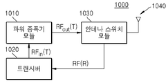
도 8을 참조하면, 시스템(1000)은 본 발명의 예시적인 실시예들에 따른 HEMT 소자들(100, 100a, 100b, 100c, 100d)을 포함하는 파워 증폭기 모듈(power amplifier module)(1010)을 포함할 수 있다. 또한, 파워 증폭기 모듈(1010)은 RF (radio frequency) 파워 증폭기 모듈일 수 있다. 이러한 시스템(1000)은 RF 파워 증폭기 모듈(1010)과 커플된 트랜시버(transceiver)(1020)를 포함할 수 있다.Referring to FIG. 8,
RF 파워 증폭기 모듈(1010)은 트랜시버(1020)로부터 RF 입력 신호(RFin(T))를 수신할 수 있고, RF 출력 신호(RFout(T))를 제공하기 위하여, 상기 RF 입력 신호(RFin(T))를 증폭할 수 있다. 이러한 RF 입력 신호(RFin(T)) 및 RF 출력 신호(RFout(T))가 도 8에 화살표로 도시된 신호들의 송신 모드(transmitting mode)에 해당할 수 있다.The RF
증폭된 RF 출력 신호(RFout(T))는 안테나 스위치 모듈(antenna switch module, ASM)(1030)에 제공될 수 있고, 이는 안테나 구조(1040)를 통한 RF 출력 신호(RFout(T))의 OTA(over-the-air) 전달을 용이하게 할 수 있다. 안테나 스위치 모듈(1030)은 또한 안테나 구조를 통해 RF 신호들(RF(R))을 수신할 수 있고, 수신된 RF 신호들(RF(R))을 트랜시버에 커플시킬 수 있고, 이는 신호들의 수신 모드(receiving mode)에 해당할 수 있다.The amplified RF output signal RFout (T) may be provided to an antenna switch module (ASM) 1030, which is an OTA of the RF output signal RFout (T) through the
예시적인 실시예들에 있어서, 안테나 구조(1040)는 하나 또는 그 이상의 방향성 및/또는 무방향성(omni-directional) 안테나들을 포함할 수 있다. 예를 들어, 안테나 구조(1040)는 다이폴 안테나, 모노폴 안테나, 패치 안테나, 루프 안테나, 마이크로스트립 안테나일 수 있다. 또한, 안테나 구조(1040)는 전술한 예시들에 한정되지 않고, RF 신호들의 OTA 전달 또는 수신을 위하여 적합한 모든 종류의 안테나일 수 있다. In example embodiments,
시스템(1000)은 파워 증폭을 포함하는 시스템일 수 있다. 예를 들어, 시스템(1000)은 고주파에서의 파워 증폭에 사용될 수 있고, 개인 이동 통신, 위성 통신, 레이더 시스템, 방송 통신, 의료 기기 등의 다양한 용도로 사용될 수 있다.
이상에서 설명한 본 발명이 전술한 실시예 및 첨부된 도면에 한정되지 않으며, 본 발명의 기술적 사상을 벗어나지 않는 범위 내에서 여러 가지 치환, 변형 및 변경이 가능하다는 것은, 본 발명이 속하는 기술분야에서 통상의 지식을 가진 자에게 있어 명백할 것이다.The present invention described above is not limited to the above-described embodiments and the accompanying drawings, and various substitutions, modifications, and changes are possible within the scope not departing from the technical spirit of the present invention. It will be evident to those who have knowledge of.
100: HEMT 소자 110: 기판
115: 버퍼층 120: 고저항 반도체층
130: 채널층 140: 채널 공급층
150: 식각 정지막 160: 반도체층 패턴
162: n형 반도체층 164: 정공 주입층
174, 176: 패시베이션층 182: 소스 전극
184: 드레인 전극 186: 게이트 전극100: HEMT element 110: substrate
115: buffer layer 120: high resistance semiconductor layer
130: channel layer 140: channel supply layer
150: etch stop film 160: semiconductor layer pattern
162: n-type semiconductor layer 164: hole injection layer
174 and 176: passivation layer 182: source electrode
184: drain electrode 186: gate electrode
Claims (10)
상기 복수 개의 반도체 층들 상에 형성되며, 실리콘 카본 질화물(SixC1-xN, 0<x<1)을 포함하는 식각 정지막;
상기 식각 정지막 상에 형성된 p형 반도체층 패턴; 및
상기 p형 반도체층 패턴 상에 형성된 게이트 전극을 포함하는 고 전자이동도 트랜지스터 소자.A plurality of semiconductor layers formed on the substrate and having a 2-Dimensional Electron Gas (DEG) layer formed therein;
An etch stop layer formed on the plurality of semiconductor layers and including silicon carbon nitride (Si x C 1-x N, 0 <x <1);
A p-type semiconductor layer pattern formed on the etch stop layer; And
A high electron mobility transistor device comprising a gate electrode formed on the p-type semiconductor layer pattern.
상기 복수 개의 반도체 층들은 상기 기판 상에 순차적으로 형성된 제1 반도체 층 및 제2 반도체 층을 포함하고,
상기 제2 반도체 층과 접하는 계면 근처의 상기 제1 반도체 층 내에 상기 2DEG 층이 형성되는 것을 특징으로 하는 고 전자이동도 트랜지스터 소자.The method of claim 1,
The plurality of semiconductor layers include a first semiconductor layer and a second semiconductor layer sequentially formed on the substrate,
And the 2DEG layer is formed in the first semiconductor layer near an interface in contact with the second semiconductor layer.
상기 p형 반도체층 패턴과 오버랩되는 상기 제1 반도체층 내에 상기 2DEG층이 형성되지 않고,
상기 제2 반도체층은 상기 제1 반도체층보다 밴드갭 에너지가 높은 물질을 포함하는 것을 특징으로 하는 고 전자이동도 트랜지스터 소자.The method of claim 2,
The 2DEG layer is not formed in the first semiconductor layer overlapping the p-type semiconductor layer pattern,
The second semiconductor layer is a high electron mobility transistor device comprising a material having a higher band gap energy than the first semiconductor layer.
상기 식각 정지막 상에서 상기 p형 반도체층 패턴의 측벽들을 둘러싸며, 절연 물질을 포함하는 패시베이션층을 더 포함하는 고 전자이동도 트랜지스터 소자.The method of claim 2,
And a passivation layer surrounding sidewalls of the p-type semiconductor layer pattern on the etch stop layer, the passivation layer including an insulating material.
상기 제1 반도체층은 갈륨 질화물을 포함하고, 상기 제2 반도체층은 알루미늄 갈륨 질화물을 포함하고,
상기 p형 반도체층 패턴은 p 도핑된 갈륨 질화물, 또는 p 도핑된 알루미늄 갈륨 질화물을 포함하는 것을 특징으로 하는 고 전자이동도 트랜지스터 소자.The method of claim 2,
The first semiconductor layer comprises gallium nitride, the second semiconductor layer comprises aluminum gallium nitride,
And the p-type semiconductor layer pattern includes p-doped gallium nitride or p-doped aluminum gallium nitride.
상기 식각 정지막은 상기 p형 반도체층 패턴의 바닥면 전체와 접촉하는 것을 특징으로 하는 고 전자이동도 트랜지스터 소자.The method of claim 1,
The etch stop layer is in contact with the entire bottom surface of the p-type semiconductor layer pattern high electron mobility transistor device.
상기 제2 반도체층 상에 형성되며, 실리콘 카본 질화물(SixC1-xN, 0<x<1)을 포함하는 식각 정지막;
상기 식각 정지막 상에 형성된 p형 반도체층 패턴;
상기 p형 반도체층 패턴 상에 형성된 n형 반도체층; 및
상기 n형 반도체층 상에 형성된 게이트 전극을 포함하는 고 전자이동도 트랜지스터 소자.A first semiconductor layer and a second semiconductor layer disposed sequentially on the substrate and having a 2DEG layer formed therein;
An etch stop layer formed on the second semiconductor layer and including silicon carbon nitride (Si x C 1-x N, 0 <x <1);
A p-type semiconductor layer pattern formed on the etch stop layer;
An n-type semiconductor layer formed on the p-type semiconductor layer pattern; And
A high electron mobility transistor device comprising a gate electrode formed on the n-type semiconductor layer.
상기 n형 반도체층은 상기 p형 반도체층 패턴의 상면 전체를 커버하고,
상기 n형 반도체층은 상기 게이트 전극으로부터 상기 p형 반도체층으로 누설되는 누설 전류를 방지하는 것을 특징으로 하는 고 전자이동도 트랜지스터 소자.The method of claim 7, wherein
The n-type semiconductor layer covers the entire upper surface of the p-type semiconductor layer pattern,
And the n-type semiconductor layer prevents leakage current leaking from the gate electrode to the p-type semiconductor layer.
상기 제2 반도체층 상에 형성된 정공 주입층;
상기 정공 주입층 상에 형성되며, 실리콘 카본 질화물(SixC1-xN, 0<x<1)을 포함하는 식각 정지막;
상기 식각 정지막 상에 형성된 p형 반도체층 패턴; 및
상기 p형 반도체층 패턴 상에 형성된 게이트 전극을 포함하는 고 전자이동도 트랜지스터 소자.A first semiconductor layer and a second semiconductor layer disposed sequentially on the substrate and having a 2DEG layer formed therein;
A hole injection layer formed on the second semiconductor layer;
An etch stop layer formed on the hole injection layer and including silicon carbon nitride (Si x C 1-x N, 0 <x <1);
A p-type semiconductor layer pattern formed on the etch stop layer; And
A high electron mobility transistor device comprising a gate electrode formed on the p-type semiconductor layer pattern.
상기 정공 주입층은 상기 제2 반도체층의 상면 전체를 커버하며,
상기 정공 주입층은 상기 게이트 전극으로부터 상기 제2 반도체층으로 누설되는 누설 전류를 방지하는 것을 특징으로 하는 고 전자이동도 트랜지스터 소자.The method of claim 9,
The hole injection layer covers the entire upper surface of the second semiconductor layer,
And the hole injection layer prevents leakage current leaking from the gate electrode to the second semiconductor layer.
Priority Applications (3)
| Application Number | Priority Date | Filing Date | Title |
|---|---|---|---|
| KR1020130025251A KR102036349B1 (en) | 2013-03-08 | 2013-03-08 | High electron mobility transistors |
| US14/097,709 US9269790B2 (en) | 2013-03-08 | 2013-12-05 | High-electron-mobility transistor |
| US14/995,622 US9379227B2 (en) | 2013-03-08 | 2016-01-14 | High-electron-mobility transistor |
Applications Claiming Priority (1)
| Application Number | Priority Date | Filing Date | Title |
|---|---|---|---|
| KR1020130025251A KR102036349B1 (en) | 2013-03-08 | 2013-03-08 | High electron mobility transistors |
Publications (2)
| Publication Number | Publication Date |
|---|---|
| KR20140110617A KR20140110617A (en) | 2014-09-17 |
| KR102036349B1 true KR102036349B1 (en) | 2019-10-24 |
Family
ID=51486737
Family Applications (1)
| Application Number | Title | Priority Date | Filing Date |
|---|---|---|---|
| KR1020130025251A Active KR102036349B1 (en) | 2013-03-08 | 2013-03-08 | High electron mobility transistors |
Country Status (2)
| Country | Link |
|---|---|
| US (2) | US9269790B2 (en) |
| KR (1) | KR102036349B1 (en) |
Cited By (2)
| Publication number | Priority date | Publication date | Assignee | Title |
|---|---|---|---|---|
| US11335802B2 (en) | 2020-04-24 | 2022-05-17 | Samsung Electronics Co., Ltd. | High electron mobility transistor and method of manufacturing the same |
| US12218233B2 (en) | 2020-03-24 | 2025-02-04 | Samsung Electronics Co., Ltd. | High electron mobility transistor and method of manufacturing the same |
Families Citing this family (54)
| Publication number | Priority date | Publication date | Assignee | Title |
|---|---|---|---|---|
| KR102021887B1 (en) * | 2013-12-09 | 2019-09-17 | 삼성전자주식회사 | Semiconductor device |
| JP6331695B2 (en) * | 2014-05-28 | 2018-05-30 | 三菱電機株式会社 | Manufacturing method of semiconductor device |
| US10325774B2 (en) | 2014-09-18 | 2019-06-18 | Intel Corporation | Wurtzite heteroepitaxial structures with inclined sidewall facets for defect propagation control in silicon CMOS-compatible semiconductor devices |
| JP2016063167A (en) * | 2014-09-19 | 2016-04-25 | 株式会社東芝 | Semiconductor device |
| US10229991B2 (en) | 2014-09-25 | 2019-03-12 | Intel Corporation | III-N epitaxial device structures on free standing silicon mesas |
| US9263453B1 (en) * | 2014-09-30 | 2016-02-16 | International Business Machines Corporation | Secondary use of aspect ratio trapping holes as eDRAM structure |
| CN107078098B (en) * | 2014-11-18 | 2021-04-06 | 英特尔公司 | CMOS circuit using N-channel and P-channel gallium nitride transistors |
| EP3235005A4 (en) | 2014-12-18 | 2018-09-12 | Intel Corporation | N-channel gallium nitride transistors |
| CN106033724A (en) * | 2015-03-09 | 2016-10-19 | 中国科学院苏州纳米技术与纳米仿生研究所 | III-family nitride reinforced HEMT and preparation method thereof |
| US10211327B2 (en) | 2015-05-19 | 2019-02-19 | Intel Corporation | Semiconductor devices with raised doped crystalline structures |
| WO2016205553A1 (en) | 2015-06-16 | 2016-12-22 | Tagore Technology, Inc. | High performance radio frequency switch |
| EP3314659A4 (en) | 2015-06-26 | 2019-01-23 | INTEL Corporation | HETEROSEPITAXIAL STRUCTURES WITH STABLE SUBSTRATE INTERFACE MATERIAL AT HIGH TEMPERATURE |
| US9941384B2 (en) * | 2015-08-29 | 2018-04-10 | Taiwan Semiconductor Manufacturing Co., Ltd. | Semiconductor device and method for fabricating the same |
| WO2017036025A1 (en) * | 2015-09-01 | 2017-03-09 | 中国科学院苏州纳米技术与纳米仿生研究所 | Iii-group nitride enhanced type hemt and preparation method therefor |
| US9871067B2 (en) * | 2015-11-17 | 2018-01-16 | Taiwan Semiconductor Manufacturing Co., Ltd. | Infrared image sensor component |
| ITUB20155862A1 (en) | 2015-11-24 | 2017-05-24 | St Microelectronics Srl | NORMALLY OFF TYPE TRANSISTOR WITH REDUCED RESISTANCE IN THE STATE ON AND RELATIVE MANUFACTURING METHOD |
| US10861942B2 (en) * | 2015-12-09 | 2020-12-08 | Intel Corporation | Tunable capacitors including III-N multi-2DEG and 3DEG structures for tunable RF filters |
| WO2017111869A1 (en) | 2015-12-24 | 2017-06-29 | Intel Corporation | Transition metal dichalcogenides (tmdcs) over iii-nitride heteroepitaxial layers |
| US9941398B2 (en) * | 2016-03-17 | 2018-04-10 | Taiwan Semiconductor Manufacturing Company Ltd. | High-electron-mobility transistor (HEMT) capable of protecting a III-V compound layer |
| JP6584987B2 (en) * | 2016-03-23 | 2019-10-02 | 株式会社東芝 | Semiconductor device |
| CN107230624A (en) * | 2016-03-25 | 2017-10-03 | 北京大学 | Gallium nitride transistor and its manufacture method |
| US10211329B2 (en) * | 2016-06-16 | 2019-02-19 | Infineon Technologies Americas Corp. | Charge trapping prevention III-Nitride transistor |
| US10741682B2 (en) * | 2016-11-17 | 2020-08-11 | Semiconductor Components Industries, Llc | High-electron-mobility transistor (HEMT) semiconductor devices with reduced dynamic resistance |
| US10388778B2 (en) * | 2016-11-18 | 2019-08-20 | Nexperia B.V. | Low resistance and leakage device |
| US10170580B2 (en) | 2017-05-23 | 2019-01-01 | Industrial Technology Research Institute | Structure of GaN-based transistor and method of fabricating the same |
| TWI681561B (en) * | 2017-05-23 | 2020-01-01 | 財團法人工業技術研究院 | Structure of gan-based transistor and method of fabricating the same |
| CN107331699A (en) * | 2017-08-16 | 2017-11-07 | 英诺赛科(珠海)科技有限公司 | GaN semiconductor devices and its preparation method and application |
| US12125888B2 (en) | 2017-09-29 | 2024-10-22 | Intel Corporation | Group III-nitride (III-N) devices with reduced contact resistance and their methods of fabrication |
| US11233053B2 (en) | 2017-09-29 | 2022-01-25 | Intel Corporation | Group III-nitride (III-N) devices with reduced contact resistance and their methods of fabrication |
| CN111527592A (en) * | 2017-12-28 | 2020-08-11 | 罗姆股份有限公司 | Nitride semiconductor device |
| US10541313B2 (en) * | 2018-03-06 | 2020-01-21 | Infineon Technologies Austria Ag | High Electron Mobility Transistor with dual thickness barrier layer |
| US20190305122A1 (en) * | 2018-03-28 | 2019-10-03 | Taiwan Semiconductor Manufacturing Company Ltd. | Semiconductor structure |
| US11309450B2 (en) * | 2018-12-20 | 2022-04-19 | Analog Devices, Inc. | Hybrid semiconductor photodetector assembly |
| CN110061053B (en) * | 2019-01-15 | 2024-07-23 | 中山大学 | Enhanced semiconductor transistor and preparation method thereof |
| US11101378B2 (en) | 2019-04-09 | 2021-08-24 | Raytheon Company | Semiconductor structure having both enhancement mode group III-N high electron mobility transistors and depletion mode group III-N high electron mobility transistors |
| WO2020217735A1 (en) | 2019-04-25 | 2020-10-29 | ローム株式会社 | Nitride semiconductor device |
| CN112447836B (en) * | 2019-08-30 | 2025-05-13 | 广东致能半导体有限公司 | A high electron mobility transistor with high withstand voltage capability |
| CN112490286B (en) * | 2019-09-12 | 2023-09-19 | 联华电子股份有限公司 | Semiconductor device and manufacturing method thereof |
| US11038048B2 (en) * | 2019-10-01 | 2021-06-15 | Taiwan Semiconductor Manufacturing Company, Ltd. | Gallium nitride-on-silicon devices |
| KR102721080B1 (en) * | 2019-10-08 | 2024-10-24 | 삼성전자주식회사 | Semiconductor device, method of fabricating the same, and display device including the same |
| US11545566B2 (en) | 2019-12-26 | 2023-01-03 | Raytheon Company | Gallium nitride high electron mobility transistors (HEMTs) having reduced current collapse and power added efficiency enhancement |
| CN113224154B (en) * | 2020-02-06 | 2023-08-08 | 联华电子股份有限公司 | High electron mobility transistor and method of making the same |
| CN113451403B (en) * | 2020-03-27 | 2026-03-03 | 世界先进积体电路股份有限公司 | High electron mobility transistor and manufacturing method thereof |
| US11362190B2 (en) * | 2020-05-22 | 2022-06-14 | Raytheon Company | Depletion mode high electron mobility field effect transistor (HEMT) semiconductor device having beryllium doped Schottky contact layers |
| US12166101B2 (en) * | 2021-02-15 | 2024-12-10 | Electronics And Telecomminications Research Institute | High-electron-mobility transistor device and method of manufacturing the same |
| US20240030327A1 (en) * | 2021-08-13 | 2024-01-25 | Innoscience (Suzhou) Technology Co., Ltd. | Semiconductor device and method for manufacturing the same |
| CN116487260A (en) * | 2022-01-14 | 2023-07-25 | 联华电子股份有限公司 | High electron mobility transistor and method of making the same |
| TWI884384B (en) * | 2022-07-27 | 2025-05-21 | 聯華電子股份有限公司 | High electron mobility transistor and method for fabricating the same |
| JP2025524880A (en) * | 2022-07-29 | 2025-08-01 | モンデ ワイヤレス インコーポレイテッド | Devices for integrated front-end circuits |
| CN117672854A (en) * | 2022-08-26 | 2024-03-08 | 联华电子股份有限公司 | A method of fabricating high electron mobility transistors |
| CN115274846B (en) * | 2022-09-26 | 2023-01-10 | 晶通半导体(深圳)有限公司 | High Electron Mobility Transistor |
| KR102901259B1 (en) | 2023-11-24 | 2025-12-18 | (재)한국나노기술원 | Semiconductor apparatus with overetch detection function and manufacturing method thereof |
| KR102731069B1 (en) | 2023-11-30 | 2024-11-15 | (재)한국나노기술원 | High electron mobility transistor and manufacturing method thereof |
| CN117855267B (en) * | 2024-03-07 | 2024-06-21 | 江苏能华微电子科技发展有限公司 | High-threshold enhanced power device and preparation method thereof |
Citations (3)
| Publication number | Priority date | Publication date | Assignee | Title |
|---|---|---|---|---|
| US20040132291A1 (en) * | 2002-02-22 | 2004-07-08 | Samsung Electronics Co., Ltd. | Method of fabricating dual damascene interconnections of microelectronic device using hybrid low k-dielectric and carbon-free inorganic filler |
| US20090146182A1 (en) * | 2007-12-10 | 2009-06-11 | Masahiro Hikita | Nitride semiconductor device and method for fabricating the same |
| WO2010118092A1 (en) * | 2009-04-08 | 2010-10-14 | Efficient Power Conversion Corporation | Back diffusion suppression structures |
Family Cites Families (22)
| Publication number | Priority date | Publication date | Assignee | Title |
|---|---|---|---|---|
| US6233438B1 (en) * | 1998-03-26 | 2001-05-15 | Ericsson Inc. | Wide-range power control systems and methods for radio frequency transmitters and mobile radiotelephones |
| JP4865189B2 (en) | 2002-02-21 | 2012-02-01 | 古河電気工業株式会社 | GaN-based field effect transistor |
| JP4705412B2 (en) | 2005-06-06 | 2011-06-22 | パナソニック株式会社 | Field effect transistor and manufacturing method thereof |
| US8183595B2 (en) | 2005-07-29 | 2012-05-22 | International Rectifier Corporation | Normally off III-nitride semiconductor device having a programmable gate |
| JP2007220895A (en) | 2006-02-16 | 2007-08-30 | Matsushita Electric Ind Co Ltd | Nitride semiconductor device and manufacturing method thereof |
| JP4755961B2 (en) | 2006-09-29 | 2011-08-24 | パナソニック株式会社 | Nitride semiconductor device and manufacturing method thereof |
| JP5186096B2 (en) | 2006-10-12 | 2013-04-17 | パナソニック株式会社 | Nitride semiconductor transistor and manufacturing method thereof |
| TWI512831B (en) | 2007-06-01 | 2015-12-11 | 美國加利福尼亞大學董事會 | GaN P-type / aluminum gallium nitride / aluminum nitride / gallium nitride enhanced field effect transistor |
| US7915643B2 (en) | 2007-09-17 | 2011-03-29 | Transphorm Inc. | Enhancement mode gallium nitride power devices |
| KR101008272B1 (en) | 2008-09-25 | 2011-01-13 | 전자부품연구원 | Nitride-based high electron mobility transistors having normal-off characteristics and a method of manufacturing the same |
| WO2010050021A1 (en) | 2008-10-29 | 2010-05-06 | 富士通株式会社 | Compound semiconductor device and method for manufacturing the same |
| JP5640325B2 (en) | 2009-04-30 | 2014-12-17 | 富士通株式会社 | Compound semiconductor device |
| JP5487749B2 (en) | 2009-06-17 | 2014-05-07 | 富士通株式会社 | Semiconductor device and manufacturing method thereof |
| WO2011007529A1 (en) * | 2009-07-14 | 2011-01-20 | パナソニック株式会社 | High-frequency power amplifier |
| JP2012004503A (en) | 2010-06-21 | 2012-01-05 | Nagoya Institute Of Technology | Semiconductor substrate and semiconductor device |
| KR101720589B1 (en) | 2010-10-11 | 2017-03-30 | 삼성전자주식회사 | E-mode High Electron Mobility Transistor and method of manufacturing the same |
| KR102065115B1 (en) | 2010-11-05 | 2020-01-13 | 삼성전자주식회사 | High Electron Mobility Transistor having E-mode and method of manufacturing the same |
| CN103348480B (en) | 2011-01-31 | 2016-11-16 | 宜普电源转换公司 | Being ion implanted and alignment grid electrode structure voluntarily for gallium nitride transistor |
| KR101882997B1 (en) * | 2011-09-30 | 2018-07-30 | 삼성전기주식회사 | Nitride semiconductor device and manufacturing method thereof |
| US8946771B2 (en) * | 2011-11-09 | 2015-02-03 | Taiwan Semiconductor Manufacturing Co., Ltd. | Gallium nitride semiconductor devices and method making thereof |
| KR101922121B1 (en) * | 2012-10-09 | 2018-11-26 | 삼성전자주식회사 | High electron mobility transistor and method of manufacturing the same |
| KR20140110616A (en) * | 2013-03-08 | 2014-09-17 | 삼성전자주식회사 | High electron mobility transistor devices |
-
2013
- 2013-03-08 KR KR1020130025251A patent/KR102036349B1/en active Active
- 2013-12-05 US US14/097,709 patent/US9269790B2/en active Active
-
2016
- 2016-01-14 US US14/995,622 patent/US9379227B2/en active Active
Patent Citations (3)
| Publication number | Priority date | Publication date | Assignee | Title |
|---|---|---|---|---|
| US20040132291A1 (en) * | 2002-02-22 | 2004-07-08 | Samsung Electronics Co., Ltd. | Method of fabricating dual damascene interconnections of microelectronic device using hybrid low k-dielectric and carbon-free inorganic filler |
| US20090146182A1 (en) * | 2007-12-10 | 2009-06-11 | Masahiro Hikita | Nitride semiconductor device and method for fabricating the same |
| WO2010118092A1 (en) * | 2009-04-08 | 2010-10-14 | Efficient Power Conversion Corporation | Back diffusion suppression structures |
Cited By (3)
| Publication number | Priority date | Publication date | Assignee | Title |
|---|---|---|---|---|
| US12218233B2 (en) | 2020-03-24 | 2025-02-04 | Samsung Electronics Co., Ltd. | High electron mobility transistor and method of manufacturing the same |
| US11335802B2 (en) | 2020-04-24 | 2022-05-17 | Samsung Electronics Co., Ltd. | High electron mobility transistor and method of manufacturing the same |
| US11757029B2 (en) | 2020-04-24 | 2023-09-12 | Samsung Electronics Co., Ltd. | High electron mobility transistor and method of manufacturing the same |
Also Published As
| Publication number | Publication date |
|---|---|
| US20140252368A1 (en) | 2014-09-11 |
| KR20140110617A (en) | 2014-09-17 |
| US9269790B2 (en) | 2016-02-23 |
| US9379227B2 (en) | 2016-06-28 |
| US20160126339A1 (en) | 2016-05-05 |
Similar Documents
| Publication | Publication Date | Title |
|---|---|---|
| KR102036349B1 (en) | High electron mobility transistors | |
| JP6554530B2 (en) | Group III nitride transistor using regrowth structure | |
| US20250098200A1 (en) | Gallium nitride enhancement mode device | |
| US20140253241A1 (en) | High electron mobility transistor device | |
| EP3284107B1 (en) | Iii-nitride transistor with trench gate | |
| US20150021616A1 (en) | Nitride-based semiconductor devices | |
| US9349819B2 (en) | Heterojunction semiconductor device and manufacturing method | |
| TWI512973B (en) | Semiconductor device and method of manufacturing the same | |
| KR102055839B1 (en) | Nitride based semiconductor device | |
| US20130240951A1 (en) | Gallium nitride superjunction devices | |
| KR101285598B1 (en) | Nitride baced heterostructure semiconductor device and manufacturing method thereof | |
| JP5900315B2 (en) | Semiconductor device and manufacturing method of semiconductor device | |
| JP2013247363A (en) | Group iii-nitride transistor with charge-inducing layer | |
| WO2014011332A1 (en) | Gallium nitride devices having low ohmic contact resistance | |
| TWI605588B (en) | Group III nitride-based transistor having a gate dielectric including a fluorine or chlorine compound | |
| US9202905B1 (en) | Digital alloy layer in a III-nitrade based heterojunction field effect transistor | |
| KR101668445B1 (en) | Semiconductor device and manufacturing method thereof | |
| KR101205872B1 (en) | GaN based semiconductor device and method of manufacturing the same | |
| KR101688965B1 (en) | Manufacturing method for semiconductor device | |
| KR20150000115A (en) | nitride-based transistor with vertical channel and method of fabricating the same | |
| WO2024000432A1 (en) | Semiconductor device and manufacturing method therefor | |
| KR101439291B1 (en) | Semiconductor and methode of manufacturing thereof | |
| KR20140055408A (en) | Normally-off nitride-based transistor using the depletion area and method of fabricating the same |
Legal Events
| Date | Code | Title | Description |
|---|---|---|---|
| PA0109 | Patent application |
St.27 status event code: A-0-1-A10-A12-nap-PA0109 |
|
| PG1501 | Laying open of application |
St.27 status event code: A-1-1-Q10-Q12-nap-PG1501 |
|
| A201 | Request for examination | ||
| PA0201 | Request for examination |
St.27 status event code: A-1-2-D10-D11-exm-PA0201 |
|
| E902 | Notification of reason for refusal | ||
| PE0902 | Notice of grounds for rejection |
St.27 status event code: A-1-2-D10-D21-exm-PE0902 |
|
| P11-X000 | Amendment of application requested |
St.27 status event code: A-2-2-P10-P11-nap-X000 |
|
| P13-X000 | Application amended |
St.27 status event code: A-2-2-P10-P13-nap-X000 |
|
| E90F | Notification of reason for final refusal | ||
| PE0902 | Notice of grounds for rejection |
St.27 status event code: A-1-2-D10-D21-exm-PE0902 |
|
| P11-X000 | Amendment of application requested |
St.27 status event code: A-2-2-P10-P11-nap-X000 |
|
| P13-X000 | Application amended |
St.27 status event code: A-2-2-P10-P13-nap-X000 |
|
| E701 | Decision to grant or registration of patent right | ||
| PE0701 | Decision of registration |
St.27 status event code: A-1-2-D10-D22-exm-PE0701 |
|
| GRNT | Written decision to grant | ||
| PR0701 | Registration of establishment |
St.27 status event code: A-2-4-F10-F11-exm-PR0701 |
|
| PR1002 | Payment of registration fee |
St.27 status event code: A-2-2-U10-U11-oth-PR1002 Fee payment year number: 1 |
|
| PG1601 | Publication of registration |
St.27 status event code: A-4-4-Q10-Q13-nap-PG1601 |
|
| FPAY | Annual fee payment |
Payment date: 20220927 Year of fee payment: 4 |
|
| PR1001 | Payment of annual fee |
St.27 status event code: A-4-4-U10-U11-oth-PR1001 Fee payment year number: 4 |
|
| PR1001 | Payment of annual fee |
St.27 status event code: A-4-4-U10-U11-oth-PR1001 Fee payment year number: 5 |
|
| PR1001 | Payment of annual fee |
St.27 status event code: A-4-4-U10-U11-oth-PR1001 Fee payment year number: 6 |
|
| P22-X000 | Classification modified |
St.27 status event code: A-4-4-P10-P22-nap-X000 |
|
| PR1001 | Payment of annual fee |
St.27 status event code: A-4-4-U10-U11-oth-PR1001 Fee payment year number: 7 |
|
| U11 | Full renewal or maintenance fee paid |
Free format text: ST27 STATUS EVENT CODE: A-4-4-U10-U11-OTH-PR1001 (AS PROVIDED BY THE NATIONAL OFFICE) Year of fee payment: 7 |
|
| P22-X000 | Classification modified |
St.27 status event code: A-4-4-P10-P22-nap-X000 |