KR102024098B1 - Display device and method of manufacturing the same - Google Patents
Display device and method of manufacturing the same Download PDFInfo
- Publication number
- KR102024098B1 KR102024098B1 KR1020130060123A KR20130060123A KR102024098B1 KR 102024098 B1 KR102024098 B1 KR 102024098B1 KR 1020130060123 A KR1020130060123 A KR 1020130060123A KR 20130060123 A KR20130060123 A KR 20130060123A KR 102024098 B1 KR102024098 B1 KR 102024098B1
- Authority
- KR
- South Korea
- Prior art keywords
- bank
- layer
- hydrophobic
- base layer
- region
- Prior art date
- Legal status (The legal status is an assumption and is not a legal conclusion. Google has not performed a legal analysis and makes no representation as to the accuracy of the status listed.)
- Active
Links
Images


Classifications
-
- H—ELECTRICITY
- H10—SEMICONDUCTOR DEVICES; ELECTRIC SOLID-STATE DEVICES NOT OTHERWISE PROVIDED FOR
- H10K—ORGANIC ELECTRIC SOLID-STATE DEVICES
- H10K59/00—Integrated devices, or assemblies of multiple devices, comprising at least one organic light-emitting element covered by group H10K50/00
- H10K59/10—OLED displays
- H10K59/12—Active-matrix OLED [AMOLED] displays
- H10K59/122—Pixel-defining structures or layers, e.g. banks
-
- H—ELECTRICITY
- H05—ELECTRIC TECHNIQUES NOT OTHERWISE PROVIDED FOR
- H05B—ELECTRIC HEATING; ELECTRIC LIGHT SOURCES NOT OTHERWISE PROVIDED FOR; CIRCUIT ARRANGEMENTS FOR ELECTRIC LIGHT SOURCES, IN GENERAL
- H05B33/00—Electroluminescent light sources
- H05B33/10—Apparatus or processes specially adapted to the manufacture of electroluminescent light sources
-
- H—ELECTRICITY
- H10—SEMICONDUCTOR DEVICES; ELECTRIC SOLID-STATE DEVICES NOT OTHERWISE PROVIDED FOR
- H10K—ORGANIC ELECTRIC SOLID-STATE DEVICES
- H10K50/00—Organic light-emitting devices
- H10K50/80—Constructional details
- H10K50/86—Arrangements for improving contrast, e.g. preventing reflection of ambient light
- H10K50/865—Arrangements for improving contrast, e.g. preventing reflection of ambient light comprising light absorbing layers, e.g. light-blocking layers
-
- H—ELECTRICITY
- H10—SEMICONDUCTOR DEVICES; ELECTRIC SOLID-STATE DEVICES NOT OTHERWISE PROVIDED FOR
- H10K—ORGANIC ELECTRIC SOLID-STATE DEVICES
- H10K59/00—Integrated devices, or assemblies of multiple devices, comprising at least one organic light-emitting element covered by group H10K50/00
- H10K59/10—OLED displays
- H10K59/12—Active-matrix OLED [AMOLED] displays
- H10K59/124—Insulating layers formed between TFT elements and OLED elements
Landscapes
- Engineering & Computer Science (AREA)
- Microelectronics & Electronic Packaging (AREA)
- Physics & Mathematics (AREA)
- Optics & Photonics (AREA)
- Manufacturing & Machinery (AREA)
- Electroluminescent Light Sources (AREA)
Abstract
실시예에 따른 표시장치는 기재층과, 상기 기재층 상에 형성되어 기재층의 상부가 노출되도록 개구 영역이 형성된 뱅크와, 상기 뱅크의 개구 영역 상에 형성된 기능층과, 상기 뱅크의 상부 영역에 형성된 소수성층을 포함한다.
상기와 같은 실시예는 뱅크의 상부 영역에만 소수성층을 형성함으로써, 기능층 형성용 용액이 균일하게 형성되는 효과가 있다.According to an exemplary embodiment, a display device includes a base layer, a bank formed on the base layer and having an opening region formed thereon so as to expose an upper portion of the base layer, a functional layer formed on the opening region of the bank, and an upper region of the bank. Hydrophobic layer formed.
In the above embodiment, the hydrophobic layer is formed only in the upper region of the bank, so that the solution for forming the functional layer is uniformly formed.
Description
실시예는 픽셀의 발광 특성을 향상시키기 위한 표시장치 및 표시장치의 제조 방법에 관한 것이다.Embodiments relate to a display device and a method of manufacturing the display device for improving light emission characteristics of a pixel.
최근에는 정보 통신 발달과 함께 표시장치가 급격하게 발전해오고 있다. 특히, 표시장치 중 유기전계발광소자는 자발광 소자로써, 별도의 백라이트 유닛을 구비하지 않아도 되므로, 다른 표시장치에 비해 얇게 형성하며 낮은 소비전력을 가질 수 있다.Recently, display devices have been rapidly developed with the development of information and communication. In particular, the organic light emitting display device of the display device is a self-light emitting device, and does not have to be provided with a separate backlight unit, and thus may be formed thinner than other display devices and may have low power consumption.
일반적인 유기전계발광소자는 기본적으로 애노드 전극, 캐소드 전극 및 상기 두 전극 사이에 개재된 유기발광패턴을 포함할 수 있다. 여기서, 애노드 전극과 캐소드 전극에서 각각 제공된 정공과 전자가 유기발광패턴에서 재결합하여 여기자를 형성하고, 상기 여기자가 불안정한 상태에서 안정한 상태로 떨어지면서 광이 발생한다.A general organic electroluminescent device may basically include an anode electrode, a cathode electrode, and an organic light emitting pattern interposed between the two electrodes. Here, holes and electrons provided from the anode electrode and the cathode electrode, respectively, recombine in the organic light emitting pattern to form excitons, and light is generated as the excitons fall from the unstable state to a stable state.
광을 형성하는 중요한 역할을 수행하는 유기발광패턴은 대면적 기판에 형성하기 위해 잉크젯 프린팅 공정을 적용하고 있으며, 유기발광물질을 일정 영역 상에 형성시키기 위해 뱅크를 필요로 하고 있다.The organic light emitting pattern, which plays an important role in forming light, applies an inkjet printing process to form a large area substrate, and requires a bank to form an organic light emitting material on a predetermined area.
종래 뱅크는 표면 전체가 소수성을 가지는 구조로 형성하고 있으나, 소수성만 고려할 뿐, 퍼짐성은 고려하지 않아 유기발광물질이 안정적으로 형성되지 않아 픽셀의 얼룩 및 개구율을 축소시키게 되며, 이는 픽셀의 발광 특성을 저하시키는 문제점가 발생된다.Conventional banks are formed in a structure having a hydrophobic surface as a whole, but only considering hydrophobicity, not considering the spreadability, the organic light emitting material is not formed stably to reduce the speckle and aperture ratio of the pixel, which reduces the emission characteristics of the pixel The problem of deterioration arises.
상기와 같은 문제점을 해결하기 위해, 실시예는 픽셀의 발광 특성을 향상시키기 위한 표시장치 및 표시장치의 제조 방법을 제공하는 것을 목적으로 한다.In order to solve the above problems, an embodiment is to provide a display device and a method of manufacturing the display device for improving the light emission characteristics of the pixel.
상술한 목적을 달성하기 위하여, 실시예에 따른 표시장치는 기재층과, 상기 기재층 상에 형성되어 기재층의 상부가 노출되도록 개구 영역이 형성된 뱅크와, 상기 뱅크의 개구 영역 상에 형성된 기능층과, 상기 뱅크의 상부 영역에 형성된 소수성층을 포함한다.In order to achieve the above object, a display device according to an embodiment includes a base layer, a bank formed on the base layer and having an opening region formed to expose an upper portion of the base layer, and a functional layer formed on the opening region of the bank. And a hydrophobic layer formed in an upper region of the bank.
또한, 상술한 목적을 달성하기 위하여, 실시예에 따른 표시장치 제조방법은 기재층을 마련하는 단계와, 상부 영역에 소수성층이 형성된 뱅크를 상기 기재층 상에 형성하는 단계와, 상기 뱅크의 개구 영역 내에 기능층을 형성하는 단계를 포함한다.In addition, in order to achieve the above object, the display device manufacturing method according to the embodiment comprises the steps of providing a base layer, forming a bank having a hydrophobic layer formed in the upper region on the base layer, the opening of the bank Forming a functional layer in the region.
실시예는 뱅크의 상부 영역에만 소수성층을 형성함으로써, 기능층 형성용 용액이 균일하게 형성되는 효과가 있다.In the embodiment, the hydrophobic layer is formed only in the upper region of the bank, so that the solution for forming the functional layer is uniformly formed.
또한, 실시예는 뱅크의 상부의 일부에만 소수성층을 형성함으로써, 기능층 형성용 용액이 인접하는 뱅크의 공급된 다른 기능층 형성용 용액과 간섭되는 것을 방지할 수 있는 효과가 있다.In addition, the embodiment forms an hydrophobic layer only on a part of the upper portion of the bank, whereby the solution for forming the functional layer can be prevented from interfering with other supplied solution for forming the functional layer in the adjacent bank.
도 1은 실시예에 따른 유기전계발광표시장치의 표시 영역의 일부를 개략적으로 나타낸 평면도이다.
도 2는 도 1의 화소에 대한 회로도이다.
도 3은 도 1의 I-I'선의 개략적인 단면도이다.
도 4는 실시예에 따른 뱅크의 구조를 나타낸 단면도이다.
도 5 내지 도 7은 실시예에 따른 뱅크의 변형예를 나타낸 단면도이다.
도 8 내지 도 12는 실시예에 따른 뱅크의 제조방법을 나타낸 단면도이다.
도 13 내지 도 16은 실시예에 따른 유기전계발광표시장치의 제조방법을 나타낸 단면도이다.1 is a plan view schematically illustrating a portion of a display area of an organic light emitting display device according to an embodiment.
FIG. 2 is a circuit diagram of the pixel of FIG. 1.
3 is a schematic cross-sectional view taken along line II ′ of FIG. 1.
4 is a cross-sectional view showing the structure of a bank according to the embodiment.
5 to 7 are cross-sectional views showing modifications of the bank according to the embodiment.
8 to 12 are cross-sectional views showing a method of manufacturing a bank according to the embodiment.
13 to 16 are cross-sectional views illustrating a method of manufacturing an organic light emitting display device according to an embodiment.
이하, 도면을 참조하여 실시예를 상세히 설명하기로 한다.
Hereinafter, exemplary embodiments will be described in detail with reference to the accompanying drawings.
도 1은 실시예에 따른 유기전계발광표시장치의 표시 영역의 일부를 개략적으로 나타낸 평면도이고, 도 2는 도 1의 화소에 대한 회로도이고, 도 3은 도 1의 I-I'선의 개략적인 단면도이다. 1 is a plan view schematically illustrating a portion of a display area of an organic light emitting display device according to an embodiment, FIG. 2 is a circuit diagram of a pixel of FIG. 1, and FIG. 3 is a schematic cross-sectional view of a line II ′ of FIG. 1. to be.
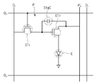
도 1 및 도 2을 참조하면, 실시예에 따른 유기전계발광표시장치는 영상을 표시하기 위한 최소한의 단위인 화소(P)를 다수개 구비할 수 있다. 1 and 2, the organic light emitting display device according to the embodiment may include a plurality of pixels P, which is a minimum unit for displaying an image.
각 화소(P)는 서로 교차하도록 배치된 게이트 배선(GL)과 데이터 배선(DL)을 통해 정의될 수 있다. 여기서, 각 화소(P)에 게이트 배선(GL)과 연결된 스위칭 박막트랜지스터(STr), 스위칭 박막트랜지스터(STr)와 연결된 구동 박막트랜지스터(DTr), 구동 박막트랜지스터(DTr)와 연결된 유기발광 다이오드(E)가 배치될 수 있다. 이에 더하여, 화소(P)에 구동 박막트랜지스터(DTr)와 유기발광다이오드(E)에 연결된 스토리지 캐패시터(StgC)가 더 배치될 수 있다.Each pixel P may be defined through a gate line GL and a data line DL disposed to cross each other. Here, each of the pixels P has a switching thin film transistor STr connected to the gate line GL, a driving thin film transistor DTr connected to the switching thin film transistor STr, and an organic light emitting diode E connected to the driving thin film transistor DTr. ) May be arranged. In addition, a storage capacitor StgC connected to the driving thin film transistor DTr and the organic light emitting diode E may be further disposed on the pixel P. FIG.
스위칭 박막트랜지스터(STr) 및 구동 박막트랜지스터(DTr)는 각각 게이트 전극, 반도체 패턴 및 소스 및 드레인 전극을 포함할 수 있다. 이때, 스위칭 박막트랜지스터(STr)의 게이트 전극은 게이트 배선(GL)과 전기적으로 연결되어 있으며, 스위칭 박막트랜지스터(STr)의 소스 전극은 데이터 배선(DL)과 전기적으로 연결되어 있을 수 있다. 또한, 스위칭 박막트랜지스터(STr)의 드레인 전극은 구동 박막트랜지스터(DTr)의 게이트 전극과 전기적으로 연결되어 있을 수 있다. The switching thin film transistor STr and the driving thin film transistor DTr may include a gate electrode, a semiconductor pattern, and a source and a drain electrode, respectively. In this case, the gate electrode of the switching thin film transistor STr may be electrically connected to the gate line GL, and the source electrode of the switching thin film transistor STr may be electrically connected to the data line DL. In addition, the drain electrode of the switching thin film transistor STr may be electrically connected to the gate electrode of the driving thin film transistor DTr.
구동 박막트랜지스터(DTr)의 소스 전극은 전원 배선(PL)과 전기적으로 연결되어 있을 수 있다. 또한, 구동 박막트랜지스터(DTr)는 유기발광다이오드(E)와 전기적으로 연결되어 있을 수 있다. The source electrode of the driving thin film transistor DTr may be electrically connected to the power line PL. In addition, the driving thin film transistor DTr may be electrically connected to the organic light emitting diode E.
유기발광다이오드(E)는 제 1 및 제 2 전극과 제 1 및 2 전극 사이에 개재된 유기발광층을 포함할 수 있다. 여기서, 유기발광층에서 제 1 및 제 2 전극 각각에서 제공된 제 1 및 제 2 전하의 재결합을 이루고, 재결합된 제 1 및 제 2 전하가 여기상태에서 기저상태로 전이되면서 광을 생성 및 방출한다.The organic light emitting diode E may include an organic light emitting layer interposed between the first and second electrodes and the first and second electrodes. Here, in the organic light emitting layer, recombination of the first and second charges provided at the first and second electrodes, respectively, and the recombined first and second charges are generated and emitted as the transition from the excited state to the ground state.
이때, 구동 박막트랜지스터(DTr)의 드레인 전극은 유기발광다이오드(E)의 제 1 전극과 전기적으로 연결되어 있을 수 있다. 이때, 전원 배선(PL)은 유기발광다이오드(E)의 제 2 전극과 전기적으로 연결되어 있을 수 있다. In this case, the drain electrode of the driving thin film transistor DTr may be electrically connected to the first electrode of the organic light emitting diode E. In this case, the power line PL may be electrically connected to the second electrode of the organic light emitting diode E.
스토리지 커패시터(StgC)는 구동 박막트랜지스터(DTr)의 게이트 전극과 소스 전극 사이에 형성되어 있을 수 있다.The storage capacitor StgC may be formed between the gate electrode and the source electrode of the driving thin film transistor DTr.
이에 따라, 게이트 신호에 따라 스위칭 박막트랜지스터는 구동 박막트랜지스터를 스위칭한다. 스위칭 박막트랜지스터의 스위칭에 의해 구동 박막트랜지스터는 데이터 신호에 따른 전류를 유기발광 다이오드에 인가한다. 유기발광 다이오드는 인가된 전류에 따른 계조를 표시할 수 있다. Accordingly, the switching thin film transistor switches the driving thin film transistor according to the gate signal. By switching the switching thin film transistor, the driving thin film transistor applies a current corresponding to the data signal to the organic light emitting diode. The organic light emitting diode may display a gray level according to the applied current.
이때, 스토리지 커패시터(StgC)는 스위칭 박막트랜지스터(STr)가 오프(off) 되었을 때 구동 박막트랜지스터(DTr)의 게이트 전압을 일정하게 유지시키는 역할을 하여, 유기발광 다이오드(E)에 흐르는 전류의 레벨은 일정하게 유지될 수 있다.In this case, the storage capacitor StgC serves to maintain a constant gate voltage of the driving thin film transistor DTr when the switching thin film transistor STr is turned off, so that the level of the current flowing through the organic light emitting diode E is maintained. Can be kept constant.
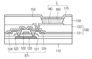
도 3에 도시된 바와 같이, 유기전계발광표시장치는 기재층(110) 상에 배치된 구동 박막트랜지스터(DTr), 구동 박막트랜지스터(DTr)를 포함한 기재층(110)상에 배치된 절연부재(130), 절연부재(130)상에 배치된 유기발광 다이오드(E)가 배치되어 있을 수 있다. As shown in FIG. 3, the organic light emitting display device includes an insulating member disposed on the
유기전계발광표시장치는 유기발광 다이오드(E)에 구비된 기능층을 습식 공정으로 형성하기 위한 뱅크(150)를 포함할 수 있다. 뱅크(150)는 상부면에 소수성 정도를 갖는 소수성층을 포함할 수 있다. 뱅크(150)는 소수 영역을 구비함에 따라, 습식공정에 의해 일정한 영역에 우수한 평탄성을 갖는 기능층을 용이하게 형성할 수 있다.The organic light emitting display device may include a
구체적으로, 실시예에 따른 유기전계발광표시장치를 설명하기로 한다. Specifically, an organic light emitting display device according to an embodiment will be described.
기재층(110)은 평탄한 기판 또는 일정한 힘에 의해 휘어질 수 있는 플렉서블한 필름일 수 있다. 기재층(110)을 형성하는 재질의 예로서는 유리, 금속 또는 플라스틱일 수 있다. The
구동 박막트랜지스터(DTr)는 기재층(110) 상에 배치된 반도체 패턴(120), 반도체 패턴(120)을 포함한 기재층(110) 상에 배치된 게이트 절연막(121), 반도체 패턴(120)의 일부 영역과 중첩되며 게이트 절연막(121) 상에 배치된 게이트 전극(122), 게이트 전극(122)을 포함한 게이트 절연막(121) 상에 배치된 층간 절연막(123), 층간 절연막(123) 상에 배치되며 반도체 패턴(120)의 소스 영역과 드레인 영역에 각각 연결된 소스 및 드레인 전극(124, 125)을 포함할 수 있다. The driving thin film transistor DTr includes a
실시예에서, 구동 박막트랜지스터(DTr)는 탑 게이트 구조를 갖는 것으로 도시 및 설명하였으나, 이에 한정하는 것은 아니다. 또한, 도면에는 도시되지 않았으나, 스위칭 박막트랜지스터는 구동 박막트랜지스터(DTr)와 동일한 형태를 가질 수 있다.In an embodiment, the driving thin film transistor DTr is illustrated and described as having a top gate structure, but is not limited thereto. In addition, although not shown in the drawing, the switching thin film transistor may have the same shape as the driving thin film transistor DTr.
절연부재(130)는 구동 박막트랜지스터(DTr)를 포함한 기재층(110)상에 배치될 수 있다. 절연부재(130)는 무기 절연막(131)과 유기 절연막(132)의 이중 구조를 가질 수 있다. 무기 절연막(131)은 산화실리콘 또는 질화실리콘으로 형성될 수 있다. The
유기 절연막(132)은 구동 박막트랜지스터(DTr) 및 다수의 배선에 의한 단차를 제거하는 평탄화기능을 수행할 수 있다. 본 실시예에서, 절연부재(130)가 이중 구조를 가지는 것으로 설명하였으나 이에 한정되는 것은 아니며, 절연부재(130)는 무기 절연막 또는 유기 절연막 중 어느 하나의 절연막 또는 무기절연막, 유기절연막 및 무기절연막의 삼중 구조를 가질 수도 있다.The
유기발광 다이오드(E)는 절연부재(130) 상에 순차적으로 배치된 화소전극(140), 적어도 유기발광층을 포함한 기능층(160), 공통전극(170)을 포함할 수 있다. The organic light emitting diode E may include a
화소전극(140)은 절연부재(130)에 형성된 콘택홀을 통해 드레인 전극(125)과 연결되어 있을 수 있다. 화소전극(140)은 각 화소영역별로 패터닝되어 있을 수 있다. The
뱅크(150)는 화소전극(140)의 에지를 따라 덮으며 비화소 영역에 배치될 수 있다. 즉, 뱅크(150)는 화소전극(140)을 노출하는 개구 영역(151)과 개구 영역(151)의 에지를 따라 배치된 측벽(152)과 화소전극(140)의 에지 및 비화소영역 상에 배치되며 측벽(152)과 연결된 상면(153)을 포함할 수 있다.The
뱅크(150)는 후술될 기능층(160), 특히 유기발광층의 형성 영역을 정의하는 역할을 할 수 있다. 또한, 뱅크(150)는 화소전극(140)과 공통전극(170)간의 쇼트를 방지하는 역할을 할 수 있다.The
뱅크(150)의 구조는 하기에서 상세하게 설명하기로 한다.The structure of the
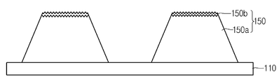
도 4는 실시예에 따른 뱅크의 구조를 나타낸 단면도이고, 도 5 내지 도 7은 실시예에 따른 뱅크의 변형예를 나타낸 단면도이다. 여기서, 설명의 편의상 기재층과 뱅크만을 도시하였다.4 is a cross-sectional view showing a structure of a bank according to the embodiment, and FIGS. 5 to 7 are cross-sectional views showing a modification of the bank according to the embodiment. Here, only the base layer and the bank are shown for convenience of description.
도 4에 도시된 바와 같이, 뱅크(150)는 기재층(110) 상에 형성되며, 뱅크(150)는 베이스층(150a)과, 소수성층(150b)을 포함한다.As shown in FIG. 4, the
베이스층(150a)의 중심 영역에는 개구 영역이 형성되며, 이로부터 기재층(110)의 상부가 노출될 수 있다. 베이스층(150a)의 측벽은 일정 각도로 기울어지도록 형성될 수 있으며, 50도 내지 70도로 기울어져 형성될 수 있다.An opening region is formed in the central region of the
베이스층(150a)의 상부에는 소수성층(150b)이 형성될 수 있다. 소수성층(150b)은 베이스층(150a)의 상부 전체면에 형성될 수 있다.The
소수성층(150b)은 폴리머 계열의 소수성 물질로 형성될 수 있으며, 폴리머 계열의 물질 이외에도 소수성 특성을 가진다면 그 재질은 한정되지 않는다. 소수성층(150b)의 표면은 불규칙적으로 형성될 수 있으며, 보다 구체적으로, 불규칙한 요철 형상으로 형성될 수 있다.The
소수성층(150b)의 표면 형상은 요철 형상 외에도 불규칙한 프리즘 형상, 반구 형상으로 형성될 수도 있다. 물론, 프리즘 형상, 반구 형상이 동시에 형성된 구조일 수도 있다.The surface shape of the
상기에서는 소수성층(150b)이 베이스층(150a)의 상부면 전체에 걸쳐 형성된 것을 도시하였으나, 이와 다르게 도 5 및 도 6에 도시된 바와 같이, 뱅크(150)의 상부면의 일부 영역에만 형성될 수도 있다.Although the
도 5를 참조하면, 다른 실시예에 따른 뱅크(150)는 기재층(110) 상에 형성되며, 뱅크(150)는 베이스층(150a)과, 소수성층(150c)을 포함한다.Referring to FIG. 5, a
베이스층(150a)의 중심 영역에는 개구 영역이 형성되며, 이로부터 기재층(110)의 상부가 노출될 수 있다. 베이스층(150a)의 상부에는 소수성층(150c)이 형성될 수 있다. 소수성층(150c)은 베이스층(150a)의 상부 중앙 영역, 예컨대, 상부 가장자리 제외한 영역에 형성될 수 있다.An opening region is formed in the central region of the
소수성층(150c)의 표면은 불규칙한 요철 형성으로 형성될 수 있으며, 베이스층(150a)의 상부 중앙 영역에 형성된 소수성층(150c)의 길이(L2)는 뱅크(150) 상부 영역의 길이(L1)의 20% 내지 80%의 길이로 형성될 수 있다.The surface of the
소수성층(150c)의 상부면은 베이스층(150a)의 상부면과 동일한 평면상에 형성될 수 있으며, 이와 다르게 소수성층(150c)의 상부면이 베이스층(150a)의 상부면으로 돌출되도록 형성될 수도 있다.The top surface of the
도 6에 도시된 바와 같이, 기능층 형성용 용액이 뱅크(150)의 상부면에 공급되면 인접하는 뱅크(150)의 공급된 다른 기능층 형성용 용액과 간섭되는 것을 방지할 수 있게 된다.As shown in FIG. 6, when the solution for forming the functional layer is supplied to the upper surface of the
도 7을 참조하면, 다른 실시예에 따른 뱅크(150)는 기재층(110) 상에 형성되며, 뱅크(150)는 베이스층(150a)과, 다수의 소수성층(150d, 150e)을 포함한다.Referring to FIG. 7, a
베이스층(150a)의 중심 영역에는 개구 영역이 형성되며, 이로부터 기재층(110)의 상부가 노출될 수 있다. 베이스층(150a)의 상부에는 소수성층(150d, 150e)이 형성될 수 있다. 소수성층(150b, 150e)은 베이스층(150a)의 상부 중앙 영역, 예컨대, 상부 가장자리 제외한 영역에 형성되며, 다수개의 소수성층이 형성될 수 있다. 소수성층의 표면은 불규칙한 요철 형성으로 형성될 수 있다.An opening region is formed in the central region of the
소수성층은 제1 소수성 부(150d)와 제2 소수성 부(150e)를 포함할 수 있다. 제1 소수성 부(150d)는 제2 소수성 부(150e)와 이격되도록 형성되며, 제1 소수성 부(150d)와 제2 소수성 부(150e)의 양 끝단의 길이(L2)는 뱅크(150) 상부 영역의 길이(L1)의 20% 내지 80%의 길이로 형성될 수 있다. 제1 소수성 부(150d) 및 제2 소수성 부(150e)의 길이(L3)는 뱅크(150) 상부 영역의 길이(L1)의 10% 내지 40%의 길이로 형성될 수 있다.The hydrophobic layer may include a first
제1 소수성 부(150d)와 제2 소수성 부(150e)의 길이는 서로 동일하게 형성될 수 있으며, 이와 다르게 서로 다른 길이로 형성될 수도 있다.The lengths of the first
도면에서는 제1 소수성 부(150d)와 제2 소수성 부(150e)의 상부면이 베이스층(150a)의 상부면과 동일 평면 상에 형성되었으나, 제1 소수성 부(150d)가 베이스층(150a)의 상부면으로 돌출되는 구조로 형성되거나, 제2 소수성 부(150e)가 베이스층(150a)의 상부면으로 돌출되는 구조를 가지도록 형성될 수 있다.In the drawing, upper surfaces of the first
상기에서 설명한 뱅크(150)의 구조로부터 기능층 형성용 용액이 뱅크(150)에 공급되면, 기능층 형성용 용액은 베이스층(150a)의 개구 영역에 안정적으로 공급될 수 있으며, 소수성층에 의해 기능층 형성용 용액이 뱅크(150)의 상부면으로 흐르는 것을 방지할 수 있게 된다.
When the solution for forming the functional layer is supplied to the
이하에서는 도 8 내지 도 12을 참조하여, 실시예에 따른 뱅크의 제조방법을 살펴본다. 도 8 내지 도 12는 실시예에 따른 뱅크의 제조방법을 나타낸 단면도이다.Hereinafter, a method of manufacturing a bank according to an embodiment will be described with reference to FIGS. 8 to 12. 8 to 12 are cross-sectional views showing a method of manufacturing a bank according to the embodiment.
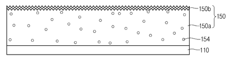
도 8에 도시된 바와 같이, 기재층(110)이 마련되면, 기재층(110) 상에 베이스층(150a)을 형성하는 단계를 수행한다. 베이스층(150a)은 감광성 수지막일 수 있다. 감광성 수지막은 폴리머 계열(Main-Polymer)의 재질로 형성될 수 있으며, 이 외에도 카도(cardo)계 수지, 노볼락계 수지, 아크릴계 수지 등이 사용될 수 있다. 감광성 수지막의 내부에는 소수성 물질(154)이 함유될 수 있다. 소수성 물질(154)은 폴리머 계열(Sub-Polymer)의 재질로 형성될 수 있다.As shown in FIG. 8, when the
베이스층(150)은 코팅법에 의해 기재층(110) 상에 형성될 수 있다.The
도 9에 도시된 바와 같이, 베이스층(150a)이 기재층(110) 상에 형성되면, 베이스층(150)에 소프트 베이킹을 수행하는 단계를 수행할 수 있다.As shown in FIG. 9, when the
베이스층(150a)은 100℃ 내지 130℃에서 약 2분 내지 5분 동안 소프트 베이킹이 수행될 수 있다.The
상기와 같이, 베이스층(150a)에 소프트 베이킹이 수행되면 베이스층(150a) 내부에 함유된 소수성 물질은 베이스층(150a)의 상부로 이동하게 되어 가교(Cross Linking)가 일어나게 된다.As described above, when the soft baking is performed on the
도 10에 도시된 바와 같이, 베이스층(150a)에 소프트 베이킹이 완료되면, 베이스층(150a) 내의 소수성 물질은 베이스층(150)의 상부로 이동하게 되어 소수성층(150b)을 형성하게 된다. 이때, 베이스층(150a) 내에 함유된 소수성 물질(154)은 일부 남아있게 된다.As shown in FIG. 10, when soft baking is completed on the
도 11에 도시된 바와 같이, 베이스층(150a)의 상부에 소수성층(150b)이 형성되면, 베이스층(150a) 상에 노광 공정을 수행하는 단계를 수행할 수 있다. As shown in FIG. 11, when the
노광 공정은 하프 톤 마스크(M)를 사용하여 수행될 수 있다. 하프 톤 마스크(M)는 중심부가 상하 개구된 구조를 가지며, 광을 차단하는 광 차단부(M1)와, 광 차단부(M1)의 내측에 형성된 그레이톤부(M2)를 포함할 수 있다.The exposure process may be performed using the halftone mask M. FIG. The halftone mask M may have a structure in which a central portion thereof is opened up and down, and may include a light blocking portion M1 for blocking light and a gray tone portion M2 formed inside the light blocking portion M1.
먼저, 하프 톤 마스크(M)를 베이스층(150a) 상에 정렬시킨다. 하프 톤 마스크(M)의 그레이톤부(M2)는 이후 형성될 뱅크(150)의 측면에 대응되는 위치에 배치될 수 있다. 그레이톤부(M2)는 광의 70% 내지 90%를 투과하는 광 투과율을 가지도록 형성될 수 있다.First, the half tone mask M is aligned on the
도 12에 도시된 바와 같이, 베이스층(150a) 상에 노광 공정을 마치면, 이후 현상 공정을 통해, 베이스층(150a)의 상부면에 소수층(150b)을 가지는 뱅크(150)가 형성될 수 있게 된다.As shown in FIG. 12, after the exposure process is completed on the
일반적으로 노광량이 많게 되면 소수성이 개선되는 반면, 퍼짐성은 저하되며, 노광량이 적게 되면 소수성은 저하되는 반면, 퍼짐성은 향상되는 특성을 가지게 된다.In general, when the exposure amount is increased, the hydrophobicity is improved, while the spreadability is lowered. When the exposure amount is decreased, the hydrophobicity is lowered, while the spreadability is improved.
베이스층(150a)의 내부에는 베이킹 공정을 수행한 다음에도 소수성 물질(154)이 남아있기 때문에 노광, 현상 공정을 수행하여 뱅크(150)를 형성하더라도, 뱅크(150)의 측면에는 소수성층이 자연적으로 형성되게 된다.Since the
하지만, 실시예에서는 뱅크(150)의 측벽에 대응되는 위치에 그레이톤부(M2)를 배치시킴으로써, 뱅크(150)의 측면은 소수성이 저하되는 반면, 퍼짐성은 향상되는 특성을 가지게 된다.However, in the exemplary embodiment, by disposing the gray tone part M2 at a position corresponding to the sidewall of the
상기에서는 하프 톤 마스크(M)의 그레이톤부(M2)를 뱅크(150)의 측벽에 대응되는 위치에 형성하였으나, 그레이톤부(M2)를 뱅크(150)의 상부 가장자리 영역과 측벽에 대응되도록 연장 형성하게 되면 뱅크(150)의 상부 중심부에만 소수성층을 형성할 수 있게 된다.In the above, the gray tone part M2 of the half tone mask M is formed at a position corresponding to the sidewall of the
뱅크(150)의 측벽에 대응되는 위치에 배치된 그레이톤부(M2)와, 뱅크(150)의 상부 가장자리 영역에 대응되는 위치에 형성된 그레이톤부(M2)의 광 투과율을 서로 다르게 형성될 수 있다.
The light transmittance of the gray tone unit M2 disposed at a position corresponding to the sidewall of the
이하에서는 도 13 내지 도 16을 참조하여, 실시예에 따른 유기전계발광표시장치의 제조방법을 살펴본다. 도 13 내지 도 16은 실시예에 따른 유기전계발광표시장치의 제조방법을 나타낸 단면도이다.Hereinafter, a method of manufacturing an organic light emitting display device according to an embodiment will be described with reference to FIGS. 13 to 16. 13 to 16 are cross-sectional views illustrating a method of manufacturing an organic light emitting display device according to an embodiment.
도 13을 참조하면, 유기전계발광표시장치를 제조하기 위해, 먼저 박막트랜지스터 기판을 형성한다. Referring to FIG. 13, to manufacture an organic light emitting display device, first, a thin film transistor substrate is formed.
구체적으로, 기재층(110) 상에 반도체 패턴(120)을 형성한다. 여기서, 반도체 패턴(120)을 형성하기 위해, 먼저 기재층 상에 증착공정을 통해 비정질 실리콘층을 형성한 후, 비정질 실리콘층을 결정화한다. 이후, 결정화된 비정질 실리콘층을 패터닝하여 반도체 패턴(120)이 형성될 수 있다. 반도체 패턴(120)을 포함한 기재층(110) 상에 게이트 절연막(121)을 형성한다. In detail, the
게이트 절연막(121)은 화학기상증착법을 통해 형성할 수 있다. 게이트 절연막(121)은 질화 실리콘 또는 산화 실리콘으로 형성될 수 있다. 반도체 패턴(120)의 채널 영역과 대응된 게이트 절연막(121) 상에 게이트 전극(122)을 형성한다. 게이트 전극(122)을 형성하는 공정에서, 게이트 전극(122)과 연결된 게이트 배선이 형성될 수 있다. The
게이트 전극(122)을 포함한 게이트 절연막(121) 상에 층간 절연막(123)을 형성한다. 층간 절연막(123)은 화학기상증착법을 통해 형성할 수 있다. 층간 절연막(123)은 질화 실리콘 또는 산화 실리콘으로 형성될 수 있다. 이후, 층간 절연막(123) 및 게이트 절연막(121)을 관통하는 비아홀을 형성한다. 비아홀은 반도체 패턴(120)의 양측의 일부, 즉 소스 및 드레인 영역을 노출할 수 있다. An interlayer insulating
층간 절연막(123) 상에 비아홀을 통해 반도체 패턴(120)의 소스 및 드레인 영역에 각각 연결되는 소스 및 드레인 전극(124, 125)을 형성한다. 이에 따라, 기재층(110) 상에 반도체 패턴(120), 게이트 절연막(121), 게이트 전극(122) 및 소스 및 드레인 전극(124, 125)을 포함한 구동 박막트랜지스터(DTr)를 형성할 수 있다.Source and
도면에는 도시되지 않았으나, 구동 박막트랜지스터(DTr)를 형성하는 공정에서 스위칭 박막트랜지스터와 스토리지 커패시터가 형성될 수 있다.Although not shown in the drawing, a switching thin film transistor and a storage capacitor may be formed in a process of forming the driving thin film transistor DTr.
구동 박막트랜지스터(DTr)를 형성한 후, 구동 박막트랜지터(DTr)를 포함한 층간 절연막(123) 상에 절연부재(130)를 형성한다. 절연부재(130)는 무기 절연막(131)과 유기절연막(132)의 이중 구조로 형성될 수 있다. After forming the driving thin film transistor DTr, the insulating
무기 절연막(131)은 화학기상증착법을 통해 형성할 수 있다. 무기 절연막(132)은 질화 실리콘 또는 산화 실리콘으로 형성될 수 있다. 유기 절연막(131)은 습식공정을 통해 형성될 수 있다. The inorganic
습식공정의 예로서는 스핀코팅법, 딥 코팅법, 잉크젯 프린팅법, 스크린 인쇄법, 다이 코팅법 및 닥터블레이드법등일 수 있다. 유기 절연막(131)을 형성하는 재질의 예로서는 포토 아크릴계 수지, 벤조사이클로부텐수지 및 폴리이미드 수지등일 수 있다.Examples of the wet process may be a spin coating method, a dip coating method, an inkjet printing method, a screen printing method, a die coating method and a doctor blade method. Examples of the material for forming the organic insulating
절연부재(130)를 형성한 후, 절연부재(130)에 구동 박막트랜지스터(DTr)의 드레인 전극(125)을 노출하는 콘택홀을 형성한다.After the insulating
이후, 콘택홀을 통해, 드레인 전극(125)과 전기적으로 연결된 화소전극(140)을 형성한다. 화소전극(140)은 도전막을 형성한 후 각 화소영역별로 식각하여 형성할 수 있다.Thereafter, the
도 14를 참조하면, 화소전극(140)을 형성한 후, 화소전극(140)을 포함한 절연부재(130) 상에 감광성 수지막(150L)을 형성한다. 감광성 수지막은 네가티브 감광성 수지막(150L)일 수 있다. 예를 들어, 감광성 수지막(150L)은 카도(cardo)계 수지, 노볼락계 수지, 및 아크릴계 수지등을 이용할 수 있으나, 본 실시예에 감광성 수지막의 재질을 한정하지 않는다. 감광성 수지막은 습식공정, 예컨대, 스핀코팅법, 딥 코팅법, 잉크젯 프린팅법, 스크린 인쇄법, 다이 코팅법 및 닥터블레이드법등을 통해 형성할 수 있다.Referring to FIG. 14, after forming the
도 15에 도시된 바와 같이, 앞서 설명한 실시예에 따른 뱅크의 제조방법에 의해 뱅크를 형성하는 단계를 수행할 수 있다.As shown in FIG. 15, a step of forming a bank may be performed by the method of manufacturing a bank according to the above-described embodiment.
도 16을 참조하면, 뱅크(150)의 형성 영역으로 기능층 형성용 용액을 습식공정으로 제공한다. 여기서, 습식 공정의 예로서는 잉크젯 프린팅법, 디스펜싱법, 스핀코팅법, 슬릿 코팅법 및 딥코팅법 중 어느 하나의 방식일 수 있다.Referring to FIG. 16, a solution for forming a functional layer is provided to the formation region of the
기능층 형성용 용액은 친수성을 가질 수 있다. 기능층 형성용 용액은 유기발광 물질을 포함한 용액일 수 있다.The solution for forming the functional layer may have hydrophilicity. The functional layer forming solution may be a solution including an organic light emitting material.
기능층 형성용 용액은 뱅크(150)의 개구영역(151)에 제공될 수 있으나, 뱅크의 상면(153)상에도 제공될 수 있다. 여기서, 기능층 형성용 용액은 뱅크(150)의 측벽(152)의 상측에서 하측으로 진행하면서 점진적으로 감소된 소수성을 가짐에 따라, 친수성의 기능층 형성용 용액은 자연적으로 뱅크(150)의 개구 영역(151)으로 이동될 수 있다.The functional layer forming solution may be provided in the
이후, 뱅크(150)의 개구 영역(151)에 배치된 기능층 형성 용액의 베이킹 공정을 수행하여, 뱅크(150)의 개구 영역(151)에 기능층(160), 즉 유기발광층이 형성될 수 있다.Thereafter, a baking process of the functional layer forming solution disposed in the
본 실시예에서, 기능층(160)으로써 유기발광층만을 형성하는 것으로 설명하였으나, 이에 한정되는 것은 아니다. 예를 들어, 도면에는 도시되지 않았으나, 유기발광 다이오드(E)의 발광효율을 증대시키기 위해, 화소전극(140)과 유기발광층 사이에 추가적인 기능층(160)으로써 정공 주입층 및 정공 수송층 중 어느 하나 또는 둘을 더 형성할 수 있다. 또한, 유기발광층과 공통전극(170) 사이에 추가적인 기능층으로써 전자주입층 및 전자수송층 중 어느 하나 또는 둘을 어느 하나 또는 둘을 더 형성할 수 있다.In the present exemplary embodiment, only the organic light emitting layer is formed as the
정공 주입층, 정공 수송층, 전자주입층 및 전자수송층 각각은 유기발광층과 같은 방법으로 형성되어 화소영역별로 패터닝되어 있을 수 있다. 또는, 정공 주입층, 정공 수송층, 전자주입층 및 전자수송층 각각은 표시영역의 전체 영역에 습식공정 또는 증착공정을 진행하여 형성될 수 있다.Each of the hole injection layer, the hole transport layer, the electron injection layer, and the electron transport layer may be formed in the same manner as the organic light emitting layer and may be patterned for each pixel region. Alternatively, each of the hole injection layer, the hole transport layer, the electron injection layer, and the electron transport layer may be formed by performing a wet process or a deposition process on the entire area of the display area.
이후, 기능층(160) 및 뱅크를 포함한 기재층상에 공통전극(170)을 형성하여, 기재층(110) 상에 화소전극(140), 기능층(160) 및 공통전극(170)을 포함한 유기발광 다이오드(E)가 형성될 수 있다.Thereafter, the
도면에는 도시되지 않았으나, 기재층(110)상에 유기발광 다이오드(E)를 밀봉하는 봉지 공정을 더 수행할 수 있다.Although not shown, an encapsulation process of sealing the organic light emitting diode E on the
상기에서는 도면 및 실시예를 참조하여 설명하였지만, 해당 기술 분야의 숙련된 당업자는 하기의 특허청구범위에 기재된 실시예의 기술적 사상으로부터 벗어나지 않는 범위 내에서 실시예는 다양하게 수정 및 변경시킬 수 있음은 이해할 수 있을 것이다.Although described above with reference to the drawings and embodiments, those skilled in the art will understand that the embodiments can be variously modified and changed without departing from the spirit of the embodiments described in the claims below. Could be.
110: 기재층 150: 뱅크
150a: 베이스층 150b: 소수성층
154:소수성 물질 M: 하프 톤 마스크
M1: 광 차단부 M2: 그레이톤부110: substrate layer 150: bank
150a:
154: hydrophobic material M: halftone mask
M1: light blocking portion M2: gray tone portion
Claims (14)
상기 기재층 상에 형성되어 기재층의 상부가 노출되도록 개구 영역이 형성된 복수의 뱅크;
상기 복수의 뱅크의 개구 영역 상에 형성된 기능층; 및
상기 복수의 뱅크의 각각의 상부 영역에 부분적으로 형성되고 소수성을 갖는 제1 소수성 부와 제2 소수성 부를 포함하고,
상기 제1 소수성 부와 상기 제2 소수성 부는 요철 형상을 갖는 표시장치.Base layer;
A plurality of banks formed on the substrate layer, the opening regions being formed to expose an upper portion of the substrate layer;
A functional layer formed on the opening regions of the plurality of banks; And
A first hydrophobic portion and a second hydrophobic portion partially formed in each upper region of the plurality of banks and having hydrophobicity,
The first hydrophobic portion and the second hydrophobic portion have a concave-convex shape.
상기 제1 소수성 부와 상기 제2 소수성 부는 서로 이격되어 형성되는 표시장치.The method of claim 1,
The first hydrophobic part and the second hydrophobic part are formed to be spaced apart from each other.
상기 제1 소수성 부와 상기 제2 소수성 부의 길이는 상기 뱅크 상부 영역의 길이의 10% 내지 40%의 길이로 형성되는 표시장치.The method of claim 1,
The length of the first hydrophobic portion and the second hydrophobic portion is 10 to 40% of the length of the upper region of the bank.
상기 제1 소수성 부와 상기 제2 소수성 부의 양 끝단의 길이는 상기 뱅크 상부 영역의 길이의 20% 내지 80%의 길이로 형성되는 표시장치.The method of claim 1,
The length of both ends of the first hydrophobic portion and the second hydrophobic portion is 20% to 80% of the length of the upper region of the bank.
상기 기능층은 유기 발광층을 포함하는 표시장치.The method of claim 1,
The functional layer includes an organic light emitting layer.
상부 영역에 소수성층이 형성된 뱅크를 상기 기재층 상에 형성하는 단계; 및
상기 뱅크의 개구 영역 내에 기능층을 형성하는 단계를 포함하고,
상기 뱅크를 형성하는 단계는 기재층 상에 베이스층을 형성하는 단계와, 상기 베이스층 상에 소프트 베이킹을 수행하는 단계와, 상기 베이스층 상에 하프 톤 마스크를 사용하여 노광 공정을 수행하는 단계와, 상기 노광된 베이스층을 현상하여 뱅크를 형성하는 단계를 포함하고,
상기 베이스층의 내부에는 소수성 물질이 함유되는 것을 특징으로 하는 표시장치의 제조방법.Preparing a substrate layer;
Forming a bank having a hydrophobic layer in an upper region on the substrate layer; And
Forming a functional layer in the opening region of the bank,
The forming of the bank may include forming a base layer on a base layer, performing soft baking on the base layer, and performing an exposure process using a halftone mask on the base layer; Developing the exposed base layer to form a bank;
And a hydrophobic material is contained in the base layer.
상기 하프 톤 마스크는 광 차단부와, 상기 광 차단부의 내측에 형성된 그레이톤부를 포함하고, 상기 그레이톤부는 광의 70% 내지 90%를 투과시키는 표시장치의 제조방법.The method of claim 8,
The half tone mask includes a light blocking part and a gray tone part formed inside the light blocking part, wherein the gray tone part transmits 70% to 90% of light.
상기 노광 공정은 그레이톤부가 뱅크의 측벽의 일부 영역과 대응되는 영역에 배치된 상태에서 수행되는 표시장치의 제조방법.The method of claim 8,
And the exposure process is performed in a state where the gray tone part is disposed in an area corresponding to a part of the sidewall of the bank.
상기 노광 공정은 그레이톤부가 뱅크의 측벽의 일부 영역과 뱅크의 상부 가장자리 영역에 대응되는 영역에 배치된 상태에서 수행되는 표시장치의 제조방법.The method of claim 8,
And the exposure process is performed in a state where the gray tone portion is disposed in a region corresponding to a portion of the sidewall of the bank and an upper edge region of the bank.
상기 뱅크의 측벽 일부에 대응되는 영역에 배치된 그레이톤부와 뱅크의 상부 가장자리 영역에 대응되는 영역에 배치된 그레이톤부의 광 투과율은 서로 다르게 형성되는 표시장치의 제조방법.The method of claim 13,
And a light transmittance of a gray tone part disposed in an area corresponding to a portion of the sidewall of the bank and a gray tone part disposed in an area corresponding to an upper edge area of the bank is different from each other.
Priority Applications (1)
| Application Number | Priority Date | Filing Date | Title |
|---|---|---|---|
| KR1020130060123A KR102024098B1 (en) | 2013-05-28 | 2013-05-28 | Display device and method of manufacturing the same |
Applications Claiming Priority (1)
| Application Number | Priority Date | Filing Date | Title |
|---|---|---|---|
| KR1020130060123A KR102024098B1 (en) | 2013-05-28 | 2013-05-28 | Display device and method of manufacturing the same |
Publications (2)
| Publication Number | Publication Date |
|---|---|
| KR20140140147A KR20140140147A (en) | 2014-12-09 |
| KR102024098B1 true KR102024098B1 (en) | 2019-09-24 |
Family
ID=52458080
Family Applications (1)
| Application Number | Title | Priority Date | Filing Date |
|---|---|---|---|
| KR1020130060123A Active KR102024098B1 (en) | 2013-05-28 | 2013-05-28 | Display device and method of manufacturing the same |
Country Status (1)
| Country | Link |
|---|---|
| KR (1) | KR102024098B1 (en) |
Cited By (2)
| Publication number | Priority date | Publication date | Assignee | Title |
|---|---|---|---|---|
| US11877478B2 (en) | 2020-08-24 | 2024-01-16 | Samsung Display Co., Ltd. | Display device |
| US11903263B2 (en) | 2021-01-08 | 2024-02-13 | Samsung Display Co., Ltd. | Method of manufacturing display device |
Families Citing this family (11)
| Publication number | Priority date | Publication date | Assignee | Title |
|---|---|---|---|---|
| KR102598922B1 (en) * | 2015-06-30 | 2023-11-06 | 엘지디스플레이 주식회사 | Organic light emitting display device and manufacturing method for the same |
| KR102368849B1 (en) * | 2015-07-30 | 2022-02-28 | 엘지디스플레이 주식회사 | Organic light emitting display device |
| KR102413120B1 (en) * | 2015-08-31 | 2022-06-24 | 엘지디스플레이 주식회사 | Organic light emitting diode display device and manufacturing method for the same |
| US10020351B2 (en) | 2016-06-24 | 2018-07-10 | Lg Display Co., Ltd. | Electroluminescence display device |
| KR102796403B1 (en) * | 2016-06-24 | 2025-04-16 | 엘지디스플레이 주식회사 | Organic light emitting display device |
| KR102735982B1 (en) * | 2016-06-30 | 2024-11-28 | 엘지디스플레이 주식회사 | Organic light emitting display device |
| KR102525822B1 (en) | 2017-07-06 | 2023-04-26 | 삼성디스플레이 주식회사 | Display device and manufacturing method thereof |
| KR102555143B1 (en) * | 2017-12-14 | 2023-07-12 | 엘지디스플레이 주식회사 | Electroluminescent Display Device |
| KR102486552B1 (en) * | 2018-01-15 | 2023-01-10 | 삼성디스플레이 주식회사 | Display device and method for manufacturing the display device |
| KR102789068B1 (en) | 2019-05-24 | 2025-04-01 | 삼성디스플레이 주식회사 | Display apparatus and manufacturing the same |
| KR20210023720A (en) * | 2019-08-21 | 2021-03-04 | 시앤양 차이훙 옵토일렉트로닉스 테크놀로지 컴퍼니 리미티드 | Manufacturing method of display panel, and display panel and display apparatus |
Citations (2)
| Publication number | Priority date | Publication date | Assignee | Title |
|---|---|---|---|---|
| KR100834344B1 (en) * | 2001-12-29 | 2008-06-02 | 엘지디스플레이 주식회사 | Active matrix organic electroluminescent device and manufacturing method thereof |
| WO2010109877A1 (en) * | 2009-03-25 | 2010-09-30 | 凸版印刷株式会社 | Organic electroluminescent device, method for manufacturing organic electroluminescent device, image display device, and method for manufacturing image display device |
Family Cites Families (4)
| Publication number | Priority date | Publication date | Assignee | Title |
|---|---|---|---|---|
| KR100783812B1 (en) * | 2006-02-23 | 2007-12-07 | 주식회사 대우일렉트로닉스 | Manufacturing method of organic light emitting element |
| KR101279296B1 (en) * | 2006-04-17 | 2013-06-26 | 엘지디스플레이 주식회사 | Organic semiconductor sturcture and methodd of manufacturing the same organic thin film transistor using the organic semiconductor sturcture and method of manufacturing the organic thin film transistor and display apparatus using the same |
| KR20100054630A (en) * | 2008-11-14 | 2010-05-25 | 엘지디스플레이 주식회사 | Organic thin film transistor, manufacturing method of the same and display device using the same |
| KR101363255B1 (en) * | 2011-12-23 | 2014-02-13 | 한국과학기술원 | Organic Thin-Film Transistor and Manufacturing Method thereof |
-
2013
- 2013-05-28 KR KR1020130060123A patent/KR102024098B1/en active Active
Patent Citations (2)
| Publication number | Priority date | Publication date | Assignee | Title |
|---|---|---|---|---|
| KR100834344B1 (en) * | 2001-12-29 | 2008-06-02 | 엘지디스플레이 주식회사 | Active matrix organic electroluminescent device and manufacturing method thereof |
| WO2010109877A1 (en) * | 2009-03-25 | 2010-09-30 | 凸版印刷株式会社 | Organic electroluminescent device, method for manufacturing organic electroluminescent device, image display device, and method for manufacturing image display device |
Cited By (2)
| Publication number | Priority date | Publication date | Assignee | Title |
|---|---|---|---|---|
| US11877478B2 (en) | 2020-08-24 | 2024-01-16 | Samsung Display Co., Ltd. | Display device |
| US11903263B2 (en) | 2021-01-08 | 2024-02-13 | Samsung Display Co., Ltd. | Method of manufacturing display device |
Also Published As
| Publication number | Publication date |
|---|---|
| KR20140140147A (en) | 2014-12-09 |
Similar Documents
| Publication | Publication Date | Title |
|---|---|---|
| KR102024098B1 (en) | Display device and method of manufacturing the same | |
| TWI549329B (en) | Organic light emitting device and method of manufacturing same | |
| US9825111B2 (en) | Method of forming thin film transistor array substrate | |
| US9024305B2 (en) | Organic light emitting diode display and method for manufacturing the same | |
| JP4145857B2 (en) | Active matrix organic light emitting display device and method for manufacturing the same | |
| CN108257547B (en) | Electroluminescent display device and method for manufacturing the same | |
| KR20140067645A (en) | Organic electro-luminescent device and method of fabricating the same | |
| WO2020010847A1 (en) | Display panel and manufacturing method therefor, and display apparatus | |
| KR20170043697A (en) | Organic light emitting display panel and method of manufacturing the same | |
| CN112670332A (en) | Pixel unit, manufacturing method thereof and display device | |
| CN111162095A (en) | Drive backplane and preparation method thereof, display panel, and display device | |
| KR20100125502A (en) | Organic light emitting display device and manufacturing method | |
| WO2019041829A1 (en) | Thin film transistor and manufacturing method, display substrate and manufacturing method, and display device | |
| KR100782461B1 (en) | TFT panel, manufacturing method thereof, and organic light emitting display device including the same | |
| JP2009070708A (en) | Display device and manufacturing method of display device | |
| JP2011014347A (en) | Light-emitting device and method for manufacturing light-emitting device | |
| CN110112142A (en) | Array substrate and its manufacturing method, display panel and electronic device | |
| CN110752220A (en) | Display substrate, preparation method thereof and display panel | |
| KR100579175B1 (en) | Manufacturing method of organic electroluminescent device | |
| KR101888941B1 (en) | Display device and method of manufacturing the same | |
| KR100623716B1 (en) | Organic electroluminescent device and manufacturing method thereof | |
| US20230309340A1 (en) | Display device and manufacturing method of display device | |
| JP2009266763A (en) | Organic el device, and display device | |
| KR102361967B1 (en) | Organic light emitting diode display device | |
| KR100712212B1 (en) | Manufacturing method of organic light emitting device |
Legal Events
| Date | Code | Title | Description |
|---|---|---|---|
| PA0109 | Patent application |
St.27 status event code: A-0-1-A10-A12-nap-PA0109 |
|
| PG1501 | Laying open of application |
St.27 status event code: A-1-1-Q10-Q12-nap-PG1501 |
|
| R17-X000 | Change to representative recorded |
St.27 status event code: A-3-3-R10-R17-oth-X000 |
|
| R17-X000 | Change to representative recorded |
St.27 status event code: A-3-3-R10-R17-oth-X000 |
|
| A201 | Request for examination | ||
| PA0201 | Request for examination |
St.27 status event code: A-1-2-D10-D11-exm-PA0201 |
|
| D13-X000 | Search requested |
St.27 status event code: A-1-2-D10-D13-srh-X000 |
|
| D14-X000 | Search report completed |
St.27 status event code: A-1-2-D10-D14-srh-X000 |
|
| E902 | Notification of reason for refusal | ||
| PE0902 | Notice of grounds for rejection |
St.27 status event code: A-1-2-D10-D21-exm-PE0902 |
|
| AMND | Amendment | ||
| E13-X000 | Pre-grant limitation requested |
St.27 status event code: A-2-3-E10-E13-lim-X000 |
|
| P11-X000 | Amendment of application requested |
St.27 status event code: A-2-2-P10-P11-nap-X000 |
|
| P13-X000 | Application amended |
St.27 status event code: A-2-2-P10-P13-nap-X000 |
|
| E601 | Decision to refuse application | ||
| PE0601 | Decision on rejection of patent |
St.27 status event code: N-2-6-B10-B15-exm-PE0601 |
|
| AMND | Amendment | ||
| E13-X000 | Pre-grant limitation requested |
St.27 status event code: A-2-3-E10-E13-lim-X000 |
|
| P11-X000 | Amendment of application requested |
St.27 status event code: A-2-2-P10-P11-nap-X000 |
|
| P13-X000 | Application amended |
St.27 status event code: A-2-2-P10-P13-nap-X000 |
|
| PX0901 | Re-examination |
St.27 status event code: A-2-3-E10-E12-rex-PX0901 |
|
| PX0701 | Decision of registration after re-examination |
St.27 status event code: A-3-4-F10-F13-rex-PX0701 |
|
| X701 | Decision to grant (after re-examination) | ||
| GRNT | Written decision to grant | ||
| PR0701 | Registration of establishment |
St.27 status event code: A-2-4-F10-F11-exm-PR0701 |
|
| PR1002 | Payment of registration fee |
St.27 status event code: A-2-2-U10-U11-oth-PR1002 Fee payment year number: 1 |
|
| PG1601 | Publication of registration |
St.27 status event code: A-4-4-Q10-Q13-nap-PG1601 |
|
| PR1001 | Payment of annual fee |
St.27 status event code: A-4-4-U10-U11-oth-PR1001 Fee payment year number: 4 |
|
| P22-X000 | Classification modified |
St.27 status event code: A-4-4-P10-P22-nap-X000 |
|
| P22-X000 | Classification modified |
St.27 status event code: A-4-4-P10-P22-nap-X000 |
|
| PR1001 | Payment of annual fee |
St.27 status event code: A-4-4-U10-U11-oth-PR1001 Fee payment year number: 5 |
|
| PR1001 | Payment of annual fee |
St.27 status event code: A-4-4-U10-U11-oth-PR1001 Fee payment year number: 6 |
|
| PR1001 | Payment of annual fee |
St.27 status event code: A-4-4-U10-U11-oth-PR1001 Fee payment year number: 7 |
|
| U11 | Full renewal or maintenance fee paid |
Free format text: ST27 STATUS EVENT CODE: A-4-4-U10-U11-OTH-PR1001 (AS PROVIDED BY THE NATIONAL OFFICE) Year of fee payment: 7 |
|
| P22-X000 | Classification modified |
St.27 status event code: A-4-4-P10-P22-nap-X000 |