KR102014172B1 - Uv light emitting device and light emitting device package - Google Patents
Uv light emitting device and light emitting device package Download PDFInfo
- Publication number
- KR102014172B1 KR102014172B1 KR1020120086365A KR20120086365A KR102014172B1 KR 102014172 B1 KR102014172 B1 KR 102014172B1 KR 1020120086365 A KR1020120086365 A KR 1020120086365A KR 20120086365 A KR20120086365 A KR 20120086365A KR 102014172 B1 KR102014172 B1 KR 102014172B1
- Authority
- KR
- South Korea
- Prior art keywords
- layer
- light emitting
- emitting device
- buffer layer
- gan
- Prior art date
- Legal status (The legal status is an assumption and is not a legal conclusion. Google has not performed a legal analysis and makes no representation as to the accuracy of the status listed.)
- Expired - Fee Related
Links
Images


Classifications
-
- H—ELECTRICITY
- H10—SEMICONDUCTOR DEVICES; ELECTRIC SOLID-STATE DEVICES NOT OTHERWISE PROVIDED FOR
- H10H—INORGANIC LIGHT-EMITTING SEMICONDUCTOR DEVICES HAVING POTENTIAL BARRIERS
- H10H20/00—Individual inorganic light-emitting semiconductor devices having potential barriers, e.g. light-emitting diodes [LED]
- H10H20/80—Constructional details
- H10H20/81—Bodies
- H10H20/816—Bodies having carrier transport control structures, e.g. highly-doped semiconductor layers or current-blocking structures
- H10H20/8162—Current-blocking structures
-
- H—ELECTRICITY
- H10—SEMICONDUCTOR DEVICES; ELECTRIC SOLID-STATE DEVICES NOT OTHERWISE PROVIDED FOR
- H10H—INORGANIC LIGHT-EMITTING SEMICONDUCTOR DEVICES HAVING POTENTIAL BARRIERS
- H10H20/00—Individual inorganic light-emitting semiconductor devices having potential barriers, e.g. light-emitting diodes [LED]
- H10H20/80—Constructional details
- H10H20/81—Bodies
- H10H20/815—Bodies having stress relaxation structures, e.g. buffer layers
-
- H—ELECTRICITY
- H10—SEMICONDUCTOR DEVICES; ELECTRIC SOLID-STATE DEVICES NOT OTHERWISE PROVIDED FOR
- H10H—INORGANIC LIGHT-EMITTING SEMICONDUCTOR DEVICES HAVING POTENTIAL BARRIERS
- H10H20/00—Individual inorganic light-emitting semiconductor devices having potential barriers, e.g. light-emitting diodes [LED]
- H10H20/80—Constructional details
- H10H20/81—Bodies
- H10H20/822—Materials of the light-emitting regions
- H10H20/824—Materials of the light-emitting regions comprising only Group III-V materials, e.g. GaP
- H10H20/825—Materials of the light-emitting regions comprising only Group III-V materials, e.g. GaP containing nitrogen, e.g. GaN
Landscapes
- Led Devices (AREA)
Abstract
실시 예는 자외선 발광 소자 및 자외선 발광 소자 패키지에 관한 것이다.
실시 예에 따른 자외선 발광 소자는, 패키지 몸체; 상기 패키지 몸체에 배치된 발광 소자; 상기 패키지 몸체에 배치되고, 상기 발광 소자와 전기적으로 연결되는 제1 전극층과 제2 전극층; 및 상기 발광 소자를 매립하는 충진재;를 포함하고, 상기 발광 소자는, 제1 도전형 반도체층과 제2 도전형 반도체층 사이에 배치된 활성층을 갖고, 자외선을 방출하는 자외선 발광 소자이고, 상기 제1 도전형 반도체층은 제1 도전층, 제1 초격자층, 제2 도전층, 제2 초격자층을 포함하고, 상기 제1 초격자층은 InGaN층/GaN층/AlGan층이 복수회로 반복된 초격자 구조이고, 상기 제2 초격자층은 n-GaN층/InGaN층/GaN층/InGan층이 복수회로 반복된 초격자 구조이고, 상기 자외선 발광 소자는, 상기 제1 도전형 반도체층 아래에 배치된 버퍼층을 더 포함하고, 상기 버퍼층은 크랙차단층을 포함하고, 상기 버퍼층은 기판 상에 적층된 제1 버퍼층; 및 상기 제1 버퍼층 상에 적층된 제2 버퍼층을 포함하고, 상기 제1 버퍼층은 저온 버퍼층이고, 상기 저온 버퍼층은 LT-GaN으로 형성되고, 250 Å의 두께로 형성되고, 상기 제2 버퍼층은 n형 또는 p형 도전형 도펀트가 도핑되지 않은 u(undoped)-GaN으로 형성되고, 15,000 Å의 두께로 형성되고, 상기 크랙차단층은 상기 제2 버퍼층에 배치되고, 알루미늄 질화갈륨층; 상기 알루미늄 질화갈륨층 상에 배치된 질화갈륨층; 및 상기 질화갈륨층 상에 배치된 인듐 질화갈륨층;이 복수회로 적층된다.Embodiments relate to an ultraviolet light emitting device and an ultraviolet light emitting device package.
Ultraviolet light emitting device according to the embodiment, the package body; A light emitting element disposed in the package body; A first electrode layer and a second electrode layer disposed on the package body and electrically connected to the light emitting device; And a filler filling the light emitting device, wherein the light emitting device is an ultraviolet light emitting device that has an active layer disposed between a first conductive semiconductor layer and a second conductive semiconductor layer, and emits ultraviolet rays. The first conductivity type semiconductor layer includes a first conductive layer, a first superlattice layer, a second conductive layer, and a second superlattice layer, and the first superlattice layer includes a plurality of InGaN, GaN, and AlGan layers. Is a superlattice structure, and the second superlattice layer is a superlattice structure in which n-GaN layer / InGaN layer / GaN layer / InGan layer is repeated a plurality of times, and the ultraviolet light emitting element is under the first conductivity type semiconductor layer. A buffer layer disposed on the substrate, the buffer layer including a crack blocking layer, wherein the buffer layer comprises: a first buffer layer stacked on a substrate; And a second buffer layer stacked on the first buffer layer, wherein the first buffer layer is a low temperature buffer layer, the low temperature buffer layer is formed of LT-GaN, has a thickness of 250 μs, and the second buffer layer is n A doped or p-type dopant is formed of undoped u-GaN, is formed to a thickness of 15,000 kPa, the crack blocking layer is disposed in the second buffer layer, and an aluminum gallium nitride layer; A gallium nitride layer disposed on the aluminum gallium nitride layer; And an indium gallium nitride layer disposed on the gallium nitride layer.
Description
실시 예는 자외선 발광 소자 및 발광 소자 패키지에 관한 것이다.Embodiments relate to an ultraviolet light emitting device and a light emitting device package.
일반적으로 질화갈륨(GaN), 질화알루미늄(AlN), 질화인듐갈륨(InGaN) 등과 같은 Ⅲ족 질화물은 열적 안정성이 우수하고, 직접 천이형 에너지 밴드(band) 구조를 갖고 있어 발광 다이오드(LED)에서 주로 사용되고 있다. 구체적으로, Ⅲ족 질화물은 청색 발광 다이오드(Blue LED)와 자외선 발광 다이오드(UV LED)에서 많이 사용되고 있다.In general, Group III nitrides such as gallium nitride (GaN), aluminum nitride (AlN), and indium gallium nitride (InGaN) have excellent thermal stability, and have a direct transition energy band structure. Mainly used. Specifically, group III nitrides are widely used in blue light emitting diodes (Blue LEDs) and ultraviolet light emitting diodes (UV LEDs).
자외선 발광 다이오드는 청색 발광 다이오드에 비해, 광 취득 효율 및 광 출력이 현저하게 뒤떨어진다는 문제가 있다. 이는 자외선 발광 다이오드의 실용화에 커다란 장벽으로 작용하고 있다.The ultraviolet light emitting diode has a problem that the light emitting efficiency and the light output are significantly inferior to the blue light emitting diode. This acts as a large barrier to the practical use of ultraviolet light emitting diodes.
근자외선 발광 다이오드(Near UV LED)는, 위폐감식, 수지 경화 및 자외선 치료 등에 사용되고 있다. 또한, 근자외선 발광 다이오드는 형광체와 조합되어 다양한 색상의 가시광선을 구현하는 조명 장치에서도 사용되고 있다.Near UV light emitting diodes (Near UV LED) are used for gastric sensitization, resin curing, and ultraviolet light treatment. In addition, near-ultraviolet light-emitting diodes are also used in lighting devices that combine visible phosphors to produce visible light of various colors.
실시 예는 고전류에서 홀의 부족 현상을 막을 수 있는 자외선 발광 소자 및 발광 소자 패키지를 제공한다.The embodiment provides an ultraviolet light emitting device and a light emitting device package capable of preventing a shortage of holes at a high current.
또한, 실시 예는 크랙을 차단할 수 있는 자외선 발광 소자 및 발광 소자 패키지를 제공한다.In addition, the embodiment provides an ultraviolet light emitting device and a light emitting device package that can block cracks.
실시 예에 따른 자외선 발광 소자는, 제1 도전형 반도체층과 제2 도전형 반도체층 사이에 배치된 활성층을 갖고, 자외선을 방출하는 자외선 발광 소자로서, 상기 제2 도전형 반도체층과 상기 활성층 사이에 배치된 전자차단층; 및 상기 전자차단층과 상기 활성층 사이에 배치된 p형 질화갈륨층;을 포함한다.The ultraviolet light emitting device according to the embodiment has an active layer disposed between the first conductivity type semiconductor layer and the second conductivity type semiconductor layer, and emits ultraviolet rays. The ultraviolet light emitting device is disposed between the second conductivity type semiconductor layer and the active layer. An electron blocking layer disposed on the; And a p-type gallium nitride layer disposed between the electron blocking layer and the active layer.
실시 예에 따른 자외선 발광 소자는, 제1 도전형 반도체층과 제2 도전형 반도체층 사이에 배치된 활성층을 갖고, 자외선을 방출하는 자외선 발광 소자로서, 상기 제1 도전형 반도체층 아래에 배치된 버퍼층을 더 포함하고, 상기 버퍼층은 크랙차단층을 포함한다.The ultraviolet light emitting device according to the embodiment has an active layer disposed between the first conductive semiconductor layer and the second conductive semiconductor layer, and emits ultraviolet light, and is disposed under the first conductive semiconductor layer. A buffer layer is further included, and the buffer layer includes a crack blocking layer.
실시 예에 따른 자외선 발광 소자 패키지는, 패키지 몸체; 상기 패키지 몸체에 배치된 발광 소자; 상기 패키지 몸체에 배치되고, 상기 발광 소자와 전기적으로 연결되는 제1 전극층과 제2 전극층; 및 상기 발광 소자를 매립하는 충진재;를 포함하고, 상기 발광 소자는, 제1 도전형 반도체층과 제2 도전형 반도체층 사이에 배치된 활성층을 갖고, 자외선을 방출하는 자외선 발광 소자이고, 상기 자외선 발광 소자는, 상기 제2 도전형 반도체층과 상기 활성층 사이에 배치된 전자차단층; 및 상기 전자차단층과 상기 활성층 사이에 배치된 p형 질화갈륨층;을 더 포함한다.Ultraviolet light emitting device package according to the embodiment, the package body; A light emitting element disposed in the package body; A first electrode layer and a second electrode layer disposed on the package body and electrically connected to the light emitting device; And a filler filling the light emitting device, wherein the light emitting device is an ultraviolet light emitting device that has an active layer disposed between a first conductive semiconductor layer and a second conductive semiconductor layer, and emits ultraviolet rays. The light emitting device includes: an electron blocking layer disposed between the second conductivity type semiconductor layer and the active layer; And a p-type gallium nitride layer disposed between the electron blocking layer and the active layer.
실시 예에 따른 자외선 발광 소자 패키지는, 패키지 몸체; 상기 패키지 몸체에 배치된 발광 소자; 상기 패키지 몸체에 배치되고, 상기 발광 소자와 전기적으로 연결되는 제1 전극층과 제2 전극층; 및 상기 발광 소자를 매립하는 충진재;를 포함하고, 상기 발광 소자는, 제1 도전형 반도체층과 제2 도전형 반도체층 사이에 배치된 활성층을 갖고, 자외선을 방출하는 자외선 발광 소자이고, 상기 자외선 발광 소자는, 상기 제1 도전형 반도체층 아래에 배치된 버퍼층을 더 포함하고, 상기 버퍼층은 크랙차단층을 포함한다.Ultraviolet light emitting device package according to the embodiment, the package body; A light emitting element disposed in the package body; A first electrode layer and a second electrode layer disposed on the package body and electrically connected to the light emitting device; And a filler filling the light emitting device, wherein the light emitting device is an ultraviolet light emitting device that has an active layer disposed between a first conductive semiconductor layer and a second conductive semiconductor layer, and emits ultraviolet rays. The light emitting device further includes a buffer layer disposed under the first conductivity type semiconductor layer, and the buffer layer includes a crack blocking layer.
실시 예에 따른 자외선 발광 소자 및 발광 소자 패키지를 사용하면, 고전류에서 홀의 부족 현상을 막을 수 있다.By using the ultraviolet light emitting device and the light emitting device package according to the embodiment, it is possible to prevent the lack of holes at high current.
또한, 크랙을 차단할 수 있다.It is also possible to block cracks.
도 1은 실시 예에 따른 자외선 발광 소자를 나타내는 도면.
도 2는 도 1에 도시된 제1 도전형 반도체층의 변형 예를 보여주는 도면.
도 3은 다른 실시 예에 따른 자외선 발광 소자를 나타내는 도면.
도 4는 도 1에 도시된 자외선 발광 소자를 수평형 발광 소자에 적용한 도면.
도 5는 도 1에 도시된 자외선 발광 소자를 수직형 발광 소자에 적용한 도면.
도 6은 실시 예에 따른 발광 소자 패키지의 단면도.1 is a view showing an ultraviolet light emitting device according to the embodiment.
FIG. 2 is a view showing a modified example of the first conductive semiconductor layer shown in FIG. 1.
3 is a view showing an ultraviolet light emitting device according to another embodiment.
4 is a view showing the ultraviolet light emitting device shown in FIG. 1 applied to a horizontal light emitting device.
FIG. 5 is a view showing the ultraviolet light emitting device shown in FIG. 1 applied to a vertical light emitting device. FIG.
6 is a cross-sectional view of a light emitting device package according to the embodiment.
도면에서 각층의 두께나 크기는 설명의 편의 및 명확성을 위하여 과장되거나 생략되거나 또는 개략적으로 도시되었다. 또한 각 구성요소의 크기는 실제크기를 전적으로 반영하는 것은 아니다.In the drawings, the thickness or size of each layer is exaggerated, omitted, or schematically illustrated for convenience and clarity of description. In addition, the size of each component does not necessarily reflect the actual size.
본 발명에 따른 실시 예의 설명에 있어서, 어느 한 element가 다른 element의 " 상(위) 또는 하(아래)(on or under)"에 형성되는 것으로 기재되는 경우에 있어, 상(위) 또는 하(아래)(on or under)는 두 개의 element가 서로 직접(directly)접촉되거나 하나 이상의 다른 element가 상기 두 element사이에 배치되어(indirectly) 형성되는 것을 모두 포함한다. 또한 “상(위) 또는 하(아래)(on or under)”으로 표현되는 경우 하나의 element를 기준으로 위쪽 방향뿐만 아니라 아래쪽 방향의 의미도 포함할 수 있다.In the description of the embodiment according to the present invention, when one element is described as being formed on the "on or under" of another element, (On or under) includes both the two elements are in direct contact with each other (directly) or one or more other elements are formed indirectly formed (indirectly) between the two elements. In addition, when expressed as “on” or “under”, it may include the meaning of the downward direction as well as the upward direction based on one element.
이하 첨부된 도면을 참조하여 실시 예에 따른 자외선 발광 소자 및 발광 소자 패키지를 설명한다.
Hereinafter, an ultraviolet light emitting device and a light emitting device package according to an embodiment will be described with reference to the accompanying drawings.
도 1은 실시 예에 따른 자외선 발광 소자를 나타내는 도면이다.1 is a view showing an ultraviolet light emitting device according to the embodiment.
도 1에 도시된 자외선 발광 소자는, 자외선 영역의 광을 방출할 수 있다. 일 예로 도 1에 도시된 자외선 발광 소자는, 360nm 이상 400nm 이하의 범위 내의 파장을 갖는 자외선 광을 방출할 수 있다.The ultraviolet light emitting device illustrated in FIG. 1 may emit light in an ultraviolet region. As an example, the ultraviolet light emitting device illustrated in FIG. 1 may emit ultraviolet light having a wavelength within a range of 360 nm to 400 nm.
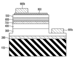
도 1을 참조하면, 실시 예에 따른 자외선 발광 소자는, 기판(100), 버퍼층(Buffer Layer, 200), 제1 도전형 반도체층(300), 활성층(Active Layer, 400), 제2 도전형 반도체층(500), 전자차단층(Electron Block Layer: EBL, 600) 및 p형 질화갈륨(p-GaN)층(700)을 포함할 수 있다.Referring to FIG. 1, the ultraviolet light emitting device according to the embodiment may include a
버퍼층(200), 제1 도전형 반도체층(300), 활성층(400), 제2 도전형 반도체층(500), 전자차단층(600) 및 p형 질화갈륨층(700) 은 화학증착방법(CVD), 분자선 에피택시법(MBE), 스퍼터링법(Sputtering), 수산화물 증기상 에피택시법(HVPE) 등의 방법에 의해 기판(100) 상에 형성될 수 있다.The
기판(100)은 C면, R면 또는 A면을 주면으로 한 사파이어(Al2O3), 스핀넬(MgAl2O4)과 같은 절연성 기판, SiC(6H, 4H, 3C를 포함함), Si, GaAs, GaN, ZnO, Si, GaP, InP, Ge 등의 반도체 기판들 중 적어도 하나일 수 있다. 여기서, 기판(100)이 상술한 재료로 한정되는 것은 아니고, 제1 도전형 반도체층(300), 활성층(400), 제2 도전형 반도체층(500), 전자차단층(600) 및 p형 질화갈륨층(700)을 순차적으로 성장시킬 수 있는 어떠한 재질의 기판도 포함하는 것으로 이해하여야 한다.
The
버퍼층(200)은 기판(100)과 제1 도전형 반도체층(300) 사이에 배치된다. 버퍼층(200)은 기판(100)과 제1 도전형 반도체층(300)의 이종접합(heterojunction)에 의해 발생될 수 있는 전위(dislocation), 깨짐(crack) 또는 뒤틀림(warp)을 완화할 수 있다.
The
버퍼층(200)은 GadAl1 -dN(d는, 0<d≤1)으로 이루어진 질화물 반도체일 수 있다. 알루미늄(Al)의 비율이 작을수록 결정성이 현저하게 개선되므로 알루미늄(Al)이 작은 질화물 반도체의 사용이 바람직하다. 따라서, 버퍼층(200)을 위한 물질로서 GaN의 사용이 가장 바람직하다.The
버퍼층(200)의 두께는 0.002 내지 0.5㎛, 바람직하게는 0.005 내지 0.2㎛, 보다 바람직하게는 0.01 내지 0.02㎛의 범위일 수 있다. 버퍼층(200)의 두께가 상기 범위에 있다면, 질화물 반도체의 결정 몰포로지(morphology)가 좋아지고, 버퍼층(200) 위에 성장시킨 제1 도전형 반도체층(300)의 결정성이 개선될 수 있다.The thickness of the
버퍼층(200)의 성장온도는, 200 내지 900℃이고, 바람직하게는 400 내지 800℃의 범위일 수 있다. 성장온도가 상기 범위라면, 성장된 버퍼층(200)은 좋은 다결정이 되고, 상기 다결정은 종결정으로서 사용되어 버퍼층(200) 위에 성장되는 제1 도전형 반도체층(300)의 결정성을 좋게 할 수 있다.The growth temperature of the
버퍼층(200)은 적어도 둘 이상의 버퍼층들이 적층된 것일 수 있다. 예를 들어, 버퍼층(200)은 기판(100) 상에 적층된 제1 버퍼층과, 제1 버퍼층 상에 적층된 제2 버퍼층을 포함할 수 있다. The
제1 버퍼층은 저온 버퍼층(Low Temperature Buffer Layer)일 수 있다. 저온 버퍼층은 LT-GaN을 재료로 채택하여 형성할 수 있다. 저온 버퍼층은 대략 250Å의 두께로 형성될 수 있다.The first buffer layer may be a low temperature buffer layer. The low temperature buffer layer can be formed by adopting LT-GaN as a material. The low temperature buffer layer may be formed to a thickness of approximately 250 μs.
제2 버퍼층은 n형 또는 p형 도전형 도펀트가 도핑되지 않은 u(undoped)-GaN을 재료로 채택하여 형성할 수 있다. u-GaN을 재료로 한 제2 버퍼층을 성장시키면 제1 도전형 반도체층(300)의 결정성을 좋게 할 수 있다.The second buffer layer may be formed by adopting u (undoped) -GaN that is not doped with an n-type or p-type conductive dopant. When the second buffer layer made of u-GaN is grown, the crystallinity of the first conductivity-
이러한 제2 버퍼층은 제1 및 제2 도전형 반도체층(300, 500)에 비해 현저히 낮은 전기 전도성을 갖는다. 제2 버퍼층은 대략 15,000Å의 두께로 형성될 수 있다.The second buffer layer has a significantly lower electrical conductivity than the first and second conductivity
한편, 버퍼층(200)은 위 제1 버퍼층과 제2 버퍼층 중 적어도 하나의 층일 수도 있다. 또한, 버퍼층(200) 자체가 실시 예에 따른 자외선 발광 소자에 포함되지 않을 수도 있다.
The
버퍼층(200) 상에는 발광 구조물이 형성된다. 발광 구조물은 제1 도전형 반도체층(300), 활성층(400), 제2 도전형 반도체층(500), 전자차단층(600) 및 p형 질화갈륨층(700)을 포함할 수 있다. 이하, 발광 구조물을 상세히 설명한다.
The light emitting structure is formed on the
제1 도전형 반도체층(300)은 예를 들어, n형 반도체층일 수 있고, 그 재질은 GaN일 수 있다. 여기서, 제1 도전형 반도체층(300)의 재질에 대해 한정하지 않는다. The first conductivity-
제1 도전형 반도체층(300)에는 Si, Ge 및 Sn 등의 n형 도펀트가 도핑된다. n형 도펀트는 3×10¹⁸/㎤ 이상, 바람직하게는 5×10¹⁸/㎤ 이상의 농도로 제1 도전형 반도체층(300)에 포함될 수 있다. 이와 같이 n형 도펀트를 많이 도핑하면, 순방향 전압(Vf) 및 임계전류를 저하시킬 수 있다. 도펀트의 농도가 상기 범위를 벗어나면 Vf가 거의 낮아지지 않을 것이다. 또한, 제1 도전형 반도체층(300)이 결정성 좋은 u-GaN 위에 형성되면, 고농도의 n형 도펀트를 함유함에도 불구하고 좋은 결정성을 가질 수 있다. n형 도펀트의 농도의 상한을 한정하지 않았음에도 불구하고 좋은 결정성을 보유하기 위해서 상기 상한은 5×10²¹/㎤ 이하로 하는 것이 바람직하다.The first
제1 도전형 반도체층(300)은 도 1에 도시된 바와 같이 단층 구조일 수도 있고, 다층 구조일 수도 있다. 다층 구조의 제1 도전형 반도체층(300)을 도 2를 참조하여 설명하도록 한다.As illustrated in FIG. 1, the first conductivity-
도 2는 도 1에 도시된 제1 도전형 반도체층(300)의 변형 예를 보여주는 도면이다.FIG. 2 is a diagram illustrating a modified example of the first
도 2를 참조하면, 제1 도전형 반도체층(300)은, 밑에서부터 순차적으로 적층된 제1 도전막(310), 제1 초격자층(320), 제2 도전층(330) 및 제2 초격자층(340)을 포함할 수 있다.Referring to FIG. 2, the first
제1 도전층(310)은 n형 반도체층으로서 그 재질은 GaN일 수 있다. 제1 도전층(310)에는 Si, Ge 및 Sn 등의 n형 도펀트가 도핑된다. 제1 도전층(310)은 대략 30,000Å의 두께로 형성될 수 있다.The first
제1 초격자층(320)은 복수의 층들이 복수회로 반복된 초격자 구조일 수 있다. 이러한 제1 초격자층(320)은 제1 층 내지 제3 층(321, 322, 323)이 대략 10회 정도 반복된 것일 수 있다. 제1 층(321)은 InGaN일 수 있고, 제2 층(322)은 GaN일 수 있으며, 제3 층(323)은 AlGaN일 수 있다. 제1 초격자층(320)은 대략 400Å의 두께로 형성될 수 있다.The
제2 도전층(330)은 n형 반도체층으로서 그 재질은 GaN일 수 있다. 제2 도전층(330)에는 Si, Ge 및 Sn 등의 n형 도펀트가 도핑될 수 있다. The second
여기서, 제2 도전층(330)은 다층 구조일 수 있다. 예를 들어, 제2 도전층(330)은 제1 두께를 갖는 제1 층과 제2 두께를 갖는 제2 층을 포함할 수 있다. 여기서, 제1 층은 n-GaN이고, 제2 층은 n-GaN층과 u-GaN층이 복수회로 교번하여 적층된 다층 구조일 수 있다.Here, the second
제2 도전층(330)의 전체 두께는 대략 14,000Å일 수 있다. 여기서, 제2 도전층(330)이 제1 층과 제2 층으로 구현되는 경우에는, 제1 층의 두께는 대략 10,000Å이고, 제2 층의 두께는 대략 4,000Å일 수 있다.The overall thickness of the second
제2 초격자층(340)은 복수의 층들이 복수회로 반복된 초격자 구조일 수 있다. 이러한 제2 초격자층(340)은 제1 층 내지 제4 층(341, 342, 343, 344)이 대략 15회 정도 반복된 것일 수 있다. 여기서, 제1 층(341)은 n-GaN이고, 제2 층(342)은 InGaN이고, 제3 층(343)은 GaN이고, 제4 층(344)은 InGaN일 수 있다. 이러한 제2 초격자층(330)은 대략 1,200Å의 두께로 형성될 수 있다.The
제1 초격자층(320)과 제2 초격자층(340)을 조합하면, 실시 예에 따른 발광 소자의 발광 출력을 보다 향상시킬 수 있고, 순방향 전압(Vf)을 보다 저하시킬 수 있다. 그 이유는 아직 분명하게 정해지지는 않았지만, 제2 초격자층(340) 위에 성장된 활성층(400)의 결정성을 보다 좋게 할 수 있기 때문으로 것으로 예상된다.
When the
다시, 도 1을 참조하면, 제1 도전형 반도체층(300) 상에 활성층(400)이 형성될 수 있다. 활성층(400)은 제1 도전형 반도체층(300)을 통해서 주입되는 전자(또는 정공)와 이후 형성되는 제2 도전형 반도체층(500)을 통해서 주입되는 정공(또는 전자)이 서로 만나서(Recombination), 활성층(400)의 형성 물질에 따른 에너지 밴드(Energy Band)의 밴드갭(Band Gap) 차이에 의해서 빛을 방출하는 층이다.Referring back to FIG. 1, an
활성층(400)은 단일 양자 우물 구조 또는 다중 양자 우물 구조(MQW: Multi Quantum Well)로 형성될 수 있다.The
활성층(400)은 일반적으로 양자 우물층과 장벽층을 포함한다. 여기서, 장벽층과 양자 우물층의 적층 순서는 특정하게 정해지지는 않으나, 양자 우물층부터 적층하여 양자 우물층으로 끝날 수도 있고, 양자 우물층부터 적층하여 장벽층으로 끝날 수도 있다. 또한, 장벽층부터 적층하여 장벽층으로 끝날 수도 있고, 장벽층부터 적층하여 양자 우물층으로 끝날 수도 있다.
The
제2 도전형 반도체층(500)은 활성층(400) 상에 형성될 수 있다. 좀 더 구체적으로, 제2 도전형 반도체층(500)은 전자차단층(600) 상에 형성될 수 있다.The second conductivity
제2 도전형 반도체층(500)은 예를 들어, p형 반도체층일 수 있고, 그 재질은 In 또는 Al을 포함하지 않는 GaN일 수 있다. 제2 도전형 반도체층(500)의 재질에 대해 한정하지 않는다.For example, the second conductivity-
제2 도전형 반도체층(500)에는 Mg, Ba 등의 p형 도펀트가 도핑된다. 여기서, p형 도펀트가 Mg이면 p형 특성이 얻어지기 용이하고, 오믹 접촉이 얻어지기 용이하다. Mg의 농도는 1×10¹⁸/㎤ 내지 1×10²¹/㎤, 바람직하게는 5×10¹⁹/㎤ 내지 3×10²⁰/㎤, 보다 바람직하게는 1×10²⁰/㎤일 수 있다. Mg 농도가 이 범위이면 좋은 p형 막이 얻어지기 용이하고 Vf를 저하시킬 수 있다.The second
여기서, 제2 도전형 반도체층(500)은 단층 구조일 수도 있고, 다층 구조일 수도 있다.
Here, the second conductivity
전자차단층(600)은 활성층(400)과 제2 도전형 반도체층(500) 사이에 배치된다. 좀 더 구체적으로, 전자차단층(600)은 p형 질화갈륨(p-GaN)층(700)과 제2 도전형 반도체층(500) 사이에 배치될 수 있다.The
전자차단층(600)은 제2 도전형 반도체층(500)보다 더 큰 에너지 밴드갭을 갖는 반도체 물질, 예를 들면 AlGaN일 수 있다. 이러한 전자차단층(600)은 제1 도전형 반도체층(300)으로부터 제공되는 전자가 활성층(400)에서 재결합되지 않고 제2 도전형 반도체층(500)으로 오버플로우되는 것을 효과적으로 방지할 수 있다.The
전자차단층(600)의 두께는 대략 300Å일 수 있다.
The thickness of the
p형 질화갈륨(p-GaN)층(700)은 활성층(400)과 전자차단층(600) 사이에 배치된다. The p-type gallium nitride (p-GaN)
더욱 구체적으로, p형 질화갈륨층(700)은 활성층(400)의 최상단에 형성된 알루미늄 질화갈륨(AlGaN)층과 전자차단층(600)의 최하단에 형성된 알루미늄 질화갈륨(AlGaN)층 사이에 배치될 수 있다.More specifically, the p-type
p형 질화갈륨층(700)이 활성층(400)과 전자차단층(600) 사이에 배치되면, 실시 예에 따른 자외선 발광 소자가 고전류에서 동작할 때, 제2 도전형 반도체층(500)에서 활성층(400)으로 유입되는 홀(hole)의 부족 현상을 해결할 수 있다.When the p-type
여기서, p형 질화갈륨층(700)의 두께는 10Å 이상 15Å 이하일 수 있다. p형 질화갈륨층(700)의 두께가 10Å보다 작으면 홀 부족 현상을 막기 어렵고, p형 질화갈륨층(700)의 두께가 15Å보다 크면 일 실시 예에 따른 자외선 발광 소자에서 방출되는 광의 파워(power)가 떨어지는 문제가 있다.
Here, the thickness of the p-type
도 1에 도시된 자외선 발광 소자의 제조 방법을 설명하도록 한다.The manufacturing method of the ultraviolet light emitting device shown in FIG. 1 will be described.
사파이어(C면)로 이루어진 기판(100)을 MOVPE의 반응용기 내에 셋팅하고, 수소를 흐르게 하여, 기판(100)의 온도를 1050℃까지 상승시키고, 기판(100)의 크리닝을 수행한다.The
다음으로, 버퍼층(200)을 기판(100) 위에 형성한다. 이하의 설명은 버퍼층(200)의 제1 버퍼층과 제2 버퍼층으로 구성된 것을 예정한 것이다. Next, the
반응용기 내의 온도를 510 ℃까지 내리고, 캐리어 가스로서 수소, 원료 가스로서 암모니아와 TMG(트리메틸가리움)을 사용하여, 기판(100)상에 GaN으로 이루어진 제1 버퍼층을 약 250Å의 두께로 성장시킨다. 상기 온도에서 성장시킨 제1 버퍼층은 기판의 종류, 성장방법 등에 따라서 생략할 수 있다. The temperature in the reaction vessel is lowered to 510 ° C., and a first buffer layer made of GaN is grown on the
제1 버퍼층을 성장 후, TMG만을 멈추고, 반응요기 내의 온도를 1050℃까지 상승시킨다. 1050℃에서, 원료가스로서 TMG, 암모니아가스를 사용하여 같은 방식으로, u-GaN으로 이루어진 제2 버퍼층을 약 15,000Å의 두께로 성장시킨다.After growing the first buffer layer, only TMG is stopped and the temperature in the reaction vessel is raised to 1050 ° C. At 1050 ° C., a second buffer layer made of u-GaN is grown to a thickness of about 15,000 kPa in the same manner using TMG and ammonia gas as source gas.
그 후, 1050℃에서, 원료가스로서 TMG, 암모니아가스, 불순물가스로서 시란(silane)가스를 사용하여 동일한 방법으로, n형 도펀트인 Si를 3 × 10¹⁹ /cm3 도핑한 GaN으로 이루어진 제1 도전형 반도체층(300)을 성장시킨다. Thereafter, at 1050 ° C., a first conductive layer consisting of GaN doped with 3 × 10 19 / cm 3 of n-type dopant in the same manner using TMG as raw material gas, ammonia gas, and silane gas as impurity gas The
다음으로, 활성층(400)을 제1 도전형 반도체층(300) 상에 성장시킨다. 구체적으로, n-AlGaN으로 이루어진 장벽층을 성장시키고, TMG, TMI, 암모니아를 사용하여 InGaN으로 이루어진 양자 우물층을 성장시킨다. 여기서, 활성층(400)은 장벽층부터 적층하지만, 적층순서는 양자 우물층부터 적층하고 우물층에서 끝나도 좋고, 또한 양자 우물층부터 적층하고 장벽층에서 끝나도 좋고, 장벽층부터 적층하고 양자 우물층에서 끝나도 좋으며, 적층순서는 특히 문제되지 않는다.Next, the
다음으로, 활성층(400) 상에 p형 질화갈륨층(700)을 성장시킨다. 여기서, p형 질화갈륨층(700)의 두께를 10Å 이상 15Å 이하가 되도록 하는 것이 바람직하다.Next, the p-type
다음으로, p형 질화갈륨층(700) 상에 전자차단층(600)을 성장시킨다. 전자차단층(600)의 재질은 AlGaN을 사용하고, 대략 300Å의 두께로 성장시킨다.Next, the
마지막으로, 전자차단층(600) 상에 제2 도전형 반도체층(500)을 성장시킨다. 구체적으로, 1050℃에서, TMG, 암모니아, Cp2Mg을 사용하여, Mg를 1 ×10²⁰/cm3 도핑한 p형 GaN으로 된 제2 도전형 반도체층(500)을 대략 850Å의 두께로 성장시킨다. 여기서, 제2 도전형 반도체층(500)은 InXAlYGa(1-X-Y)N(0≤X, 0≤Y, X+Y≤1)으로 구성될 수 있어, 그 조성은 특히 한정되지 않지만, 바람직하게는 GaN으로 하면 결정 결함이 적은 층을 얻기 쉽고, 또한 p전극 재료와 바람직한 오믹 접촉이 얻어지기 쉽다.
Finally, the second conductivity
도 3은 다른 실시 예에 따른 자외선 발광 소자를 나타내는 도면이다.3 is a view showing an ultraviolet light emitting device according to another embodiment.
도 3을 참조하면, 다른 실시 예에 따른 자외선 발광 소자는, 기판(100), 버퍼층(200’), 제1 도전형 반도체층(300), 활성층(400) 및 제2 도전형 반도체층(500)을 포함할 수 있다. 기판(100), 제1 도전형 반도체층(300), 활성층(400) 및 제2 도전형 반도체층(500)은 도 1에 도시된 기판(100), 제1 도전형 반도체층(300), 활성층(400) 및 제2 도전형 반도체층(500)과 동일하므로, 구체적인 설명은 앞서 상술한 내용으로 대체한다.Referring to FIG. 3, an ultraviolet light emitting device according to another embodiment may include a
다른 실시 예에 따른 자외선 발광 소자가 도 1에 도시된 발광 다이오드와 다른 점 중 하나로서, 버퍼층(200’)이 크랙차단층(Crack Block Layer, 250’)을 포함한다는 것이다.The ultraviolet light emitting device according to another embodiment is different from the light emitting diode shown in FIG. 1, and the
버퍼층(200’)에 관한 내용은 도 1에 도시된 버퍼층(200)과 같다. 따라서, 구체적인 설명은 앞서 설명한 내용으로 대체한다.The contents of the buffer layer 200 'are the same as the
크랙차단층(250’)은 버퍼층(200’)에서도 특히, u-GaN으로 형성된 제2 버퍼층에 배치될 수 있다. The crack blocking layer 250 'may be disposed in the buffer layer 200', in particular, in the second buffer layer formed of u-GaN.
크랙차단층(250’)은 알루미늄 질화갈륨(AlGaN)층(251’), 알루미늄 질화갈륨층(251’) 상에 배치된 질화갈륨(GaN)층(253’) 및 질화갈륨층(253’) 상에 배치된 인듐 질화갈륨(InGaN)층(255’)를 포함할 수 있다. The crack blocking layer 250 'includes an aluminum gallium nitride (AlGaN)
상기 AlGaN-GaN-InGaN 구조의 크랙차단층(250’)은 격자 상수가 서로 다른 이종접합에 의한 크랙(Crack)의 발생을 막을 수 있다. 이는 인듐 질화갈륨층(255’)의 형성 시 생기는 V-디펙트(defect)가 크랙차단층(250’) 아래에 생기는 크랙과 크랙차단층(250’) 위에 생기는 크랙의 연결을 끊기 때문이다. 따라서, 인듐 질화갈륨층(255’)의 V-defect 특성에 의해, 크랙차단층(250’)은 다른 실시 예에 따른 자외선 발광 소자의 적층 구조에서 수직방향으로 길게 생길 수 있는 크랙을 중간에서 차단할 수 있다. 여기서, 크랙차단층(250’)은 인듐 질화갈륨으로 한정되는 것은 아니고, 층 형성 시 V-defect을 형성하는 어떠한 반도체 물질도 가능하다.The crack blocking layer 250 'of the AlGaN-GaN-InGaN structure can prevent cracks due to heterojunctions having different lattice constants. This is because the V-defect generated when the indium gallium nitride layer 255 'is disconnected from the crack that occurs under the crack blocking layer 250' and the crack occurring on the crack blocking layer 250 '. Therefore, due to the V-defect characteristic of the indium gallium nitride layer 255 ', the crack blocking layer 250' may block a crack, which may occur in the vertical direction, in the middle in the laminated structure of the ultraviolet light emitting device according to another embodiment. Can be. The
크랙차단층(250’)은 초격자 구조일 수 있다. 구체적으로, 크랙차단층(250’)은 순차적으로 적층된 알루미늄 질화갈륨층(251’), 질화갈륨층(253’) 및 인듐 질화갈륨층(255’)이 10회 이상 또는 15회 이하 적층된 초격자 구조일 수 있다. The
크랙차단층(250’)의 전체 두께는 40nm 이하일 수 있다.The total thickness of the
한편, 크랙차단층(250’)에서, 알루미늄 질화갈륨층(251’)과 인듐 질화갈륨층(255’)의 위치는 서로 바뀔 수도 있다.
In the
도 4는 도 1에 도시된 자외선 발광 소자를 수평형 발광 소자에 적용한 도면이다.4 is a diagram illustrating the ultraviolet light emitting device shown in FIG. 1 applied to a horizontal light emitting device.
도 4에 도시된 수평형 발광 소자는, 도 1에 도시된 자외선 발광 소자에 메사 에칭(Mesa Etching)을 수행하여 제1 도전형 반도체층(300)의 일부가 노출되도록 하고, 노출된 제1 도전형 반도체층(300) 상에 제1 전극(900a)을 형성하여 구현할 수 있다.In the horizontal light emitting device illustrated in FIG. 4, a portion of the first
제2 도전형 반도체층(500) 상에는 투명 전극층(800)이 형성될 수 있다. 투명 전극층(800)은 ITO, IZO(In-ZnO), GZO(Ga-ZnO), AZO(Al-ZnO), AGZO(Al-Ga ZnO), IGZO(In-Ga ZnO), IrOx, RuOx, RuOx/ITO, Ni/IrOx/Au 및 Ni/IrOx/Au/ITO 중 적어도 하나를 포함하며, 이러한 재료로 한정하지는 않는다. 투명 전극층(800)은 제2 도전형 반도체층(500)과 제2 전극(900b)을 오믹 접촉시킬 수 있다.The
한편, 투명 전극층(800) 대신 반사 전극층이 형성될 수도 있으며, 반사 전극층은 반사율이 높은 은(Ag), 은(Ag)을 포함하는 합금, 알루미늄(Al) 또는 알루미늄(Al)을 포함하는 합금 중 적어도 어느 하나로 형성될 수 있다.Meanwhile, a reflective electrode layer may be formed instead of the
투명 전극층(800) 상에는 제2 전극(900b)이 형성될 수 있다. 제2 전극(900b)은 제1 전극(900a)과 함께 수평형 발광 소자에 전원을 제공한다.The
한편, 도면에 도시하지 않았으나, 도 3에 도시된 다른 실시 예에 따른 자외선 발광 소자도 도 4와 같은 수평형 발광 소자에 적용할 수 있음은 당연하다.
On the other hand, although not shown in the drawings, it is obvious that the ultraviolet light emitting device according to another embodiment shown in Figure 3 can also be applied to the horizontal light emitting device as shown in FIG.
도 5는 도 1에 도시된 자외선 발광 소자를 수직형 발광 소자에 적용한 도면이다.FIG. 5 is a view showing the ultraviolet light emitting device shown in FIG. 1 applied to a vertical light emitting device.
도 5에 도시된 수직형 발광 소자는, 도 1에 도시된 발광 소자의 제2 도전형 반도체층(500) 상에 반사층(800’)과 전도성 지지부재(900b’)을 형성하고, 도 1에 도시된 기판(100)을 제거하여 형성할 수 있다.In the vertical light emitting device shown in FIG. 5, the
반사층(800’)은 제2 도전형 반도체층(500) 상에 형성될 수 있다. 반사층(800’)은 반사율이 높은 은(Ag), 은(Ag)을 포함하는 합금, 알루미늄(Al), 알루미늄(Al)을 포함하는 합금, 백금(Pt) 또는 백금(Pt)을 포함하는 합금 중 적어도 어느 하나로 형성될 수 있다.The
반사층(800’) 상에는 전도성 지지부재(900b’)가 형성될 수 있다. 전도성 지지부재(900b’)는 도 5에 도시된 수직형 발광 소자에 전원을 제공한다.The
전도성 지지부재(900b’)는 티탄(Ti), 크롬(Cr), 니켈(Ni), 알루미늄(Al), 백금(Pt), 금(Au), 텅스텐(W), 구리(Cu), 몰리브덴(Mo) 또는 불순물이 주입된 반도체 기판 중 적어도 어느 하나로 형성될 수 있다.The
한편, 전도성 지지부재(900b’)와 반사층(800’) 사이에는 두 층 사이의 계면 접합력을 향상시키는 접착층(미도시)이 더 형성될 수 있다. 또한, 제2 도전형 반도체층(500)과 반사층(800’) 사이에는 두 층 사이의 오믹 접촉을 위해 오믹층(미도시)이 더 형성될 수 있다.Meanwhile, an adhesive layer (not shown) may be further formed between the
도 1에 도시된 기판(100)은 레이저 리프트 오프(LLO) 공정에 의해 제거되거나, 에칭 공정에 의해 제거될 수 있으며, 이에 대해 한정하지는 않는다. 기판(100)을 제거한 후, 버퍼층(200)과 제1 도전형 반도체층(300)의 일부는 에칭 공정, 예를 들어 ICP/RIE(Inductively coupled Plasma / Reactive Ion Etching)에 의해 제거될 수 있으나, 이에 대해 한정하지는 않는다.The
기판(100)이 제거된 후, 노출된 제1 도전형 반도체층(300)과 버퍼층(200) 중 어느 하나에는 전극(900a’)이 형성될 수 있다. 전극(900a’)은 전도성 지지부재(900b’)와 함께 실시 예에 따른 수직형 발광 소자에 전원을 제공한다.After the
한편, 도면에 도시하지 않았으나, 도 3에 도시된 다른 실시 예에 따른 자외선 발광 소자도 도 5와 같은 수직형 발광 소자에 적용할 수 있음은 당연하다.
On the other hand, although not shown in the drawings, it is obvious that the ultraviolet light emitting device according to another embodiment shown in Figure 3 can also be applied to the vertical light emitting device as shown in FIG.
도 6은 실시 예에 따른 발광 소자 패키지의 단면도이다. 6 is a cross-sectional view of a light emitting device package according to the embodiment.
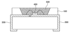
도 6을 참조하면, 실시 예에 따른 발광 소자 패키지는, 패키지 몸체(1000), 패키지 몸체(1000)에 형성된 제1 전극층(2000)과 제2 전극층(3000), 패키지 몸체(1000)에 설치되어 제1 전극층(2000) 및 제2 전극층(3000)과 전기적으로 연결된 발광 소자(4000) 및 발광 소자(4000)를 매립하는 충진재(5000)를 포함할 수 있다.Referring to FIG. 6, the light emitting device package according to the embodiment may be installed on the
패키지 몸체(1000)는 실리콘 재질, 합성수지 재질, 또는 금속 재질을 포함하여 형성될 수 있으며, 발광 소자(4000) 주위에 형성된 경사면을 가질 수 있다. 경사면은 발광 소자 패키지의 광 추출 효율을 높일 수 있다.The
제1 전극층(2000) 및 제2 전극층(3000)은 서로 전기적으로 분리되며, 발광 소자(4000)에 전원을 제공한다. 또한, 제1 전극층(2000) 및 제2 전극층(3000)은 발광 소자(4000)에서 발생된 광을 반사시켜 광 효율을 증가시킬 수 있으며, 발광 소자(4000)에서 발생된 열을 외부로 배출시키는 역할을 할 수 있다.The
발광 소자(4000)는 패키지 몸체(1000) 상에 배치되거나, 제1 전극층(2000) 또는 제2 전극층(3000) 상에 배치될 수 있다. 발광 소자(4000)는 제1 전극층(2000) 및 제2 전극층(3000)과 와이어 방식, 플립칩 방식 또는 다이 본딩 방식 중 어느 하나에 의해 전기적으로 연결될 수 있다. The
발광 소자(4000)는 도 4 내지 도 5에 도시된 발광 소자 중 어느 하나일 수 있다. 따라서, 발광 소자(4000)는 자외선 영역의 광을 방출할 수 있다. 일 예로, 발광 소자(4000)는 360nm 이상 400nm 이하의 범위 내의 자외선을 방출할 수 있다.The
충진재(5000)는 발광 소자(4000)를 매립하여 보호한다. 또한, 충진재(5000)에는 형광체가 포함되어 발광 소자(4000)에서 방출된 광의 파장을 변화시킬 수 있다.
도 6에 도시된 발광 소자 패키지는 상기에 개시된 실시 예들의 발광 소자 중 적어도 하나를 하나 또는 복수개로 탑재할 수 있으며, 이에 대해 한정하지는 않는다.The light emitting device package illustrated in FIG. 6 may mount at least one or more light emitting devices of the above-described embodiments, but is not limited thereto.
실시 예에 따른 발광 소자 패키지는 복수개가 기판 상에 배열되며, 발광 소자 패키지의 광 경로 상에 광학 부재인 도광판, 프리즘 시트, 확산 시트 등이 배치될 수 있다. 이러한 발광 소자 패키지, 기판, 광학 부재는 라이트 유닛으로 기능할 수 있다. 또 다른 실시 예는 상술한 실시 예들에 기재된 반도체 발광 소자 또는 발광 소자 패키지를 포함하는 표시 장치, 지시 장치, 조명 시스템으로 구현될 수 있으며, 예를 들어, 조명 시스템은 램프, 가로등을 포함할 수 있다.
A plurality of light emitting device packages according to the embodiment may be arranged on a substrate, and a light guide plate, a prism sheet, a diffusion sheet, or the like, which is an optical member, may be disposed on an optical path of the light emitting device package. The light emitting device package, the substrate, and the optical member may function as a light unit. Another embodiment may be implemented as a display device, an indicator device, or a lighting system including the semiconductor light emitting device or the light emitting device package described in the above embodiments, and for example, the lighting system may include a lamp or a street lamp. .
이상에서 실시 예를 중심으로 설명하였으나 이는 단지 예시일 뿐 본 발명을 한정하는 것이 아니며, 본 발명이 속하는 분야의 통상의 지식을 가진 자라면 본 실시예의 본질적인 특성을 벗어나지 않는 범위에서 이상에 예시되지 않은 여러 가지의 변형과 응용이 가능함을 알 수 있을 것이다. 예를 들어, 실시 예에 구체적으로 나타난 각 구성 요소는 변형하여 실시할 수 있는 것이다. 그리고 이러한 변형과 응용에 관계된 차이점들은 첨부된 청구 범위에서 규정하는 본 발명의 범위에 포함되는 것으로 해석되어야 할 것이다.
Although the above description has been made with reference to the embodiments, these are only examples and are not intended to limit the present invention, and those of ordinary skill in the art to which the present invention pertains should not be exemplified above without departing from the essential characteristics of the present embodiments. It will be appreciated that many variations and applications are possible. For example, each component specifically shown in the embodiment can be modified. And differences relating to such modifications and applications will have to be construed as being included in the scope of the invention defined in the appended claims.
100: 기판
200: 버퍼층
250: 크랙차단층
300: 제1 도전형 반도체층
400: 활성층
500: 제2 도전형 반도체층
600: 전자차단층
700: p-GaN층100: substrate
200: buffer layer
250: crack blocking layer
300: first conductive semiconductor layer
400: active layer
500: second conductivity type semiconductor layer
600: electronic blocking layer
700: p-GaN layer
Claims (14)
상기 패키지 몸체에 배치된 발광 소자;
상기 패키지 몸체에 배치되고, 상기 발광 소자와 전기적으로 연결되는 제1 전극층과 제2 전극층; 및
상기 발광 소자를 매립하는 충진재;를 포함하고,
상기 발광 소자는, 제1 도전형 반도체층과 제2 도전형 반도체층 사이에 배치된 활성층을 갖고, 자외선을 방출하는 자외선 발광 소자이고,
상기 제1 도전형 반도체층은 제1 도전층, 제1 초격자층, 제2 도전층, 제2 초격자층을 포함하고,
상기 제1 초격자층은 InGaN층/GaN층/AlGan층이 복수회로 반복된 초격자 구조이고,
상기 제2 초격자층은 n-GaN층/InGaN층/GaN층/InGan층이 복수회로 반복된 초격자 구조이고,
상기 자외선 발광 소자는, 상기 제1 도전형 반도체층 아래에 배치된 버퍼층을 더 포함하고,
상기 버퍼층은 크랙차단층을 포함하고,
상기 버퍼층은
기판 상에 적층된 제1 버퍼층; 및
상기 제1 버퍼층 상에 적층된 제2 버퍼층을 포함하고,
상기 제1 버퍼층은 저온 버퍼층이고, 상기 저온 버퍼층은 LT-GaN으로 형성되고, 250 Å의 두께로 형성되고,
상기 제2 버퍼층은 n형 또는 p형 도전형 도펀트가 도핑되지 않은 u(undoped)-GaN으로 형성되고, 15,000 Å의 두께로 형성되고,
상기 크랙차단층은
상기 제2 버퍼층에 배치되고, 알루미늄 질화갈륨층; 상기 알루미늄 질화갈륨층 상에 배치된 질화갈륨층; 및 상기 질화갈륨층 상에 배치된 인듐 질화갈륨층;이 복수회로 적층된, 자외선 발광 소자 패키지.Package body;
A light emitting element disposed in the package body;
A first electrode layer and a second electrode layer disposed on the package body and electrically connected to the light emitting device; And
It includes; filling the light emitting element;
The light emitting element is an ultraviolet light emitting element having an active layer disposed between the first conductivity type semiconductor layer and the second conductivity type semiconductor layer and emitting ultraviolet rays,
The first conductive semiconductor layer includes a first conductive layer, a first superlattice layer, a second conductive layer, and a second superlattice layer,
The first superlattice layer has a superlattice structure in which an InGaN layer / GaN layer / AlGan layer is repeated a plurality of times,
The second superlattice layer has a superlattice structure in which n-GaN layer / InGaN layer / GaN layer / InGan layer is repeated a plurality of times.
The ultraviolet light emitting device further includes a buffer layer disposed under the first conductivity type semiconductor layer,
The buffer layer includes a crack blocking layer,
The buffer layer
A first buffer layer stacked on the substrate; And
A second buffer layer stacked on the first buffer layer,
The first buffer layer is a low temperature buffer layer, the low temperature buffer layer is formed of LT-GaN, is formed to a thickness of 250 Å,
The second buffer layer is formed of u (undoped) -GaN without an n-type or p-type conductive dopant, and is formed to a thickness of 15,000 kHz,
The crack blocking layer
An aluminum gallium nitride layer disposed on the second buffer layer; A gallium nitride layer disposed on the aluminum gallium nitride layer; And an indium gallium nitride layer disposed on the gallium nitride layer.
상기 제1 초격자층의 두께는 400 Å이고, 상기 제2 초격자층의 두께는 1,200 Å인, 자외선 발광 소자 패키지.The method of claim 11,
The thickness of the first superlattice layer is 400 GPa, the thickness of the second superlattice layer is 1,200 GPa, UV light emitting device package.
상기 제2 도전형 반도체층은 p-GaN으로 형성되고, 850 Å의 두께로 형성되는, 자외선 발광 소자 패키지.The method of claim 11,
The second conductive semiconductor layer is formed of p-GaN, the ultraviolet light emitting device package is formed to a thickness of 850 kHz.
Priority Applications (1)
| Application Number | Priority Date | Filing Date | Title |
|---|---|---|---|
| KR1020120086365A KR102014172B1 (en) | 2012-08-07 | 2012-08-07 | Uv light emitting device and light emitting device package |
Applications Claiming Priority (1)
| Application Number | Priority Date | Filing Date | Title |
|---|---|---|---|
| KR1020120086365A KR102014172B1 (en) | 2012-08-07 | 2012-08-07 | Uv light emitting device and light emitting device package |
Publications (2)
| Publication Number | Publication Date |
|---|---|
| KR20140020026A KR20140020026A (en) | 2014-02-18 |
| KR102014172B1 true KR102014172B1 (en) | 2019-08-26 |
Family
ID=50267228
Family Applications (1)
| Application Number | Title | Priority Date | Filing Date |
|---|---|---|---|
| KR1020120086365A Expired - Fee Related KR102014172B1 (en) | 2012-08-07 | 2012-08-07 | Uv light emitting device and light emitting device package |
Country Status (1)
| Country | Link |
|---|---|
| KR (1) | KR102014172B1 (en) |
Citations (2)
| Publication number | Priority date | Publication date | Assignee | Title |
|---|---|---|---|---|
| JP2006510234A (en) * | 2003-06-25 | 2006-03-23 | エルジー イノテック カンパニー リミテッド | Nitride semiconductor light emitting device and manufacturing method thereof |
| JP2007180499A (en) * | 2005-12-28 | 2007-07-12 | Samsung Electro Mech Co Ltd | Nitride semiconductor light emitting device |
Family Cites Families (2)
| Publication number | Priority date | Publication date | Assignee | Title |
|---|---|---|---|---|
| CA2322490C (en) * | 1998-03-12 | 2010-10-26 | Nichia Chemical Industries, Ltd. | Nitride semiconductor device |
| KR100541104B1 (en) * | 2004-02-18 | 2006-01-11 | 삼성전기주식회사 | Nitride semiconductor light emitting device |
-
2012
- 2012-08-07 KR KR1020120086365A patent/KR102014172B1/en not_active Expired - Fee Related
Patent Citations (2)
| Publication number | Priority date | Publication date | Assignee | Title |
|---|---|---|---|---|
| JP2006510234A (en) * | 2003-06-25 | 2006-03-23 | エルジー イノテック カンパニー リミテッド | Nitride semiconductor light emitting device and manufacturing method thereof |
| JP2007180499A (en) * | 2005-12-28 | 2007-07-12 | Samsung Electro Mech Co Ltd | Nitride semiconductor light emitting device |
Also Published As
| Publication number | Publication date |
|---|---|
| KR20140020026A (en) | 2014-02-18 |
Similar Documents
| Publication | Publication Date | Title |
|---|---|---|
| KR101007136B1 (en) | Light emitting device, light emitting device package and manufacturing method | |
| US9991424B2 (en) | Light-emitting diode and method for manufacturing same | |
| TWI455359B (en) | Ultraviolet semiconductor light-emitting element | |
| KR101007087B1 (en) | Light emitting device and fabrication method thereof | |
| KR101134731B1 (en) | Light emitting device and method for fabricating the same | |
| US10243103B2 (en) | Ultraviolet light emitting diode, light emitting diode package, and lighting device | |
| KR20130066870A (en) | Semiconductor light emitting device | |
| US20130134475A1 (en) | Semiconductor light emitting device | |
| KR20110072424A (en) | Light emitting device, light emitting device package and manufacturing method | |
| KR20130042784A (en) | Nitride semiconductor light emitting device | |
| KR101081129B1 (en) | Light emitting device and fabrication method thereof | |
| JP2009302314A (en) | GaN-BASED SEMICONDUCTOR DEVICE | |
| KR20140020028A (en) | Uv light emitting device and light emitting device package | |
| KR101007078B1 (en) | Light emitting device and manufacturing method | |
| KR101924372B1 (en) | Uv light emitting device and light emitting device package | |
| US20070187697A1 (en) | Nitride based MQW light emitting diode having carrier supply layer | |
| KR20110117963A (en) | Nitride semiconductor light emitting device and manufacturing method thereof | |
| KR102199997B1 (en) | Light emitting device and light emitting device package | |
| KR20160086603A (en) | Light emitting device | |
| JP6482388B2 (en) | Nitride semiconductor light emitting device | |
| KR101919109B1 (en) | Uv light emitting deviceand uv light emitting device package | |
| KR102014172B1 (en) | Uv light emitting device and light emitting device package | |
| KR20220011771A (en) | Uv light emitting device, light emitting device package and lighting device | |
| JP2011082248A (en) | Semiconductor light emitting element and method of manufacturing the same, and lamp | |
| KR102397266B1 (en) | Light emitting device and lighting apparatus |
Legal Events
| Date | Code | Title | Description |
|---|---|---|---|
| PA0109 | Patent application |
St.27 status event code: A-0-1-A10-A12-nap-PA0109 |
|
| PG1501 | Laying open of application |
St.27 status event code: A-1-1-Q10-Q12-nap-PG1501 |
|
| PN2301 | Change of applicant |
St.27 status event code: A-3-3-R10-R13-asn-PN2301 St.27 status event code: A-3-3-R10-R11-asn-PN2301 |
|
| R18-X000 | Changes to party contact information recorded |
St.27 status event code: A-3-3-R10-R18-oth-X000 |
|
| P22-X000 | Classification modified |
St.27 status event code: A-2-2-P10-P22-nap-X000 |
|
| A201 | Request for examination | ||
| E13-X000 | Pre-grant limitation requested |
St.27 status event code: A-2-3-E10-E13-lim-X000 |
|
| P11-X000 | Amendment of application requested |
St.27 status event code: A-2-2-P10-P11-nap-X000 |
|
| P13-X000 | Application amended |
St.27 status event code: A-2-2-P10-P13-nap-X000 |
|
| PA0201 | Request for examination |
St.27 status event code: A-1-2-D10-D11-exm-PA0201 |
|
| E902 | Notification of reason for refusal | ||
| PE0902 | Notice of grounds for rejection |
St.27 status event code: A-1-2-D10-D21-exm-PE0902 |
|
| R18-X000 | Changes to party contact information recorded |
St.27 status event code: A-3-3-R10-R18-oth-X000 |
|
| P11-X000 | Amendment of application requested |
St.27 status event code: A-2-2-P10-P11-nap-X000 |
|
| P13-X000 | Application amended |
St.27 status event code: A-2-2-P10-P13-nap-X000 |
|
| E90F | Notification of reason for final refusal | ||
| PE0902 | Notice of grounds for rejection |
St.27 status event code: A-1-2-D10-D21-exm-PE0902 |
|
| E13-X000 | Pre-grant limitation requested |
St.27 status event code: A-2-3-E10-E13-lim-X000 |
|
| P11-X000 | Amendment of application requested |
St.27 status event code: A-2-2-P10-P11-nap-X000 |
|
| P13-X000 | Application amended |
St.27 status event code: A-2-2-P10-P13-nap-X000 |
|
| E701 | Decision to grant or registration of patent right | ||
| PE0701 | Decision of registration |
St.27 status event code: A-1-2-D10-D22-exm-PE0701 |
|
| GRNT | Written decision to grant | ||
| PR0701 | Registration of establishment |
St.27 status event code: A-2-4-F10-F11-exm-PR0701 |
|
| PR1002 | Payment of registration fee |
St.27 status event code: A-2-2-U10-U11-oth-PR1002 Fee payment year number: 1 |
|
| PG1601 | Publication of registration |
St.27 status event code: A-4-4-Q10-Q13-nap-PG1601 |
|
| R18-X000 | Changes to party contact information recorded |
St.27 status event code: A-5-5-R10-R18-oth-X000 |
|
| PN2301 | Change of applicant |
St.27 status event code: A-5-5-R10-R13-asn-PN2301 St.27 status event code: A-5-5-R10-R11-asn-PN2301 |
|
| PN2301 | Change of applicant |
St.27 status event code: A-5-5-R10-R11-asn-PN2301 |
|
| PN2301 | Change of applicant |
St.27 status event code: A-5-5-R10-R14-asn-PN2301 |
|
| FPAY | Annual fee payment |
Payment date: 20220708 Year of fee payment: 4 |
|
| PR1001 | Payment of annual fee |
St.27 status event code: A-4-4-U10-U11-oth-PR1001 Fee payment year number: 4 |
|
| PC1903 | Unpaid annual fee |
St.27 status event code: A-4-4-U10-U13-oth-PC1903 Not in force date: 20230821 Payment event data comment text: Termination Category : DEFAULT_OF_REGISTRATION_FEE |
|
| PC1903 | Unpaid annual fee |
St.27 status event code: N-4-6-H10-H13-oth-PC1903 Ip right cessation event data comment text: Termination Category : DEFAULT_OF_REGISTRATION_FEE Not in force date: 20230821 |
|
| P22-X000 | Classification modified |
St.27 status event code: A-4-4-P10-P22-nap-X000 |