KR101906967B1 - 나노갭 센서 및 이의 제조 방법 - Google Patents
나노갭 센서 및 이의 제조 방법 Download PDFInfo
- Publication number
- KR101906967B1 KR101906967B1 KR1020120035600A KR20120035600A KR101906967B1 KR 101906967 B1 KR101906967 B1 KR 101906967B1 KR 1020120035600 A KR1020120035600 A KR 1020120035600A KR 20120035600 A KR20120035600 A KR 20120035600A KR 101906967 B1 KR101906967 B1 KR 101906967B1
- Authority
- KR
- South Korea
- Prior art keywords
- nano
- electrode
- micropore
- region
- forming
- Prior art date
- Legal status (The legal status is an assumption and is not a legal conclusion. Google has not performed a legal analysis and makes no representation as to the accuracy of the status listed.)
- Active
Links
Images


Classifications
-
- G—PHYSICS
- G01—MEASURING; TESTING
- G01N—INVESTIGATING OR ANALYSING MATERIALS BY DETERMINING THEIR CHEMICAL OR PHYSICAL PROPERTIES
- G01N15/00—Investigating characteristics of particles; Investigating permeability, pore-volume or surface-area of porous materials
- G01N15/10—Investigating individual particles
- G01N15/1031—Investigating individual particles by measuring electrical or magnetic effects
-
- B—PERFORMING OPERATIONS; TRANSPORTING
- B82—NANOTECHNOLOGY
- B82Y—SPECIFIC USES OR APPLICATIONS OF NANOSTRUCTURES; MEASUREMENT OR ANALYSIS OF NANOSTRUCTURES; MANUFACTURE OR TREATMENT OF NANOSTRUCTURES
- B82Y15/00—Nanotechnology for interacting, sensing or actuating, e.g. quantum dots as markers in protein assays or molecular motors
-
- G—PHYSICS
- G01—MEASURING; TESTING
- G01N—INVESTIGATING OR ANALYSING MATERIALS BY DETERMINING THEIR CHEMICAL OR PHYSICAL PROPERTIES
- G01N15/00—Investigating characteristics of particles; Investigating permeability, pore-volume or surface-area of porous materials
- G01N15/10—Investigating individual particles
- G01N15/1023—Microstructural devices for non-optical measurement
-
- G—PHYSICS
- G01—MEASURING; TESTING
- G01N—INVESTIGATING OR ANALYSING MATERIALS BY DETERMINING THEIR CHEMICAL OR PHYSICAL PROPERTIES
- G01N27/00—Investigating or analysing materials by the use of electric, electrochemical, or magnetic means
- G01N27/02—Investigating or analysing materials by the use of electric, electrochemical, or magnetic means by investigating impedance
-
- G—PHYSICS
- G01—MEASURING; TESTING
- G01N—INVESTIGATING OR ANALYSING MATERIALS BY DETERMINING THEIR CHEMICAL OR PHYSICAL PROPERTIES
- G01N33/00—Investigating or analysing materials by specific methods not covered by groups G01N1/00 - G01N31/00
- G01N33/48—Biological material, e.g. blood, urine; Haemocytometers
- G01N33/483—Physical analysis of biological material
- G01N33/487—Physical analysis of biological material of liquid biological material
- G01N33/48707—Physical analysis of biological material of liquid biological material by electrical means
- G01N33/48721—Investigating individual macromolecules, e.g. by translocation through nanopores
-
- G—PHYSICS
- G01—MEASURING; TESTING
- G01N—INVESTIGATING OR ANALYSING MATERIALS BY DETERMINING THEIR CHEMICAL OR PHYSICAL PROPERTIES
- G01N15/00—Investigating characteristics of particles; Investigating permeability, pore-volume or surface-area of porous materials
- G01N2015/0038—Investigating nanoparticles
Landscapes
- Chemical & Material Sciences (AREA)
- Health & Medical Sciences (AREA)
- Life Sciences & Earth Sciences (AREA)
- Engineering & Computer Science (AREA)
- Physics & Mathematics (AREA)
- General Health & Medical Sciences (AREA)
- Biochemistry (AREA)
- Analytical Chemistry (AREA)
- General Physics & Mathematics (AREA)
- Immunology (AREA)
- Pathology (AREA)
- Biomedical Technology (AREA)
- Nanotechnology (AREA)
- Dispersion Chemistry (AREA)
- Molecular Biology (AREA)
- Spectroscopy & Molecular Physics (AREA)
- Biophysics (AREA)
- Hematology (AREA)
- Urology & Nephrology (AREA)
- Food Science & Technology (AREA)
- Medicinal Chemistry (AREA)
- Crystallography & Structural Chemistry (AREA)
- Chemical Kinetics & Catalysis (AREA)
- Electrochemistry (AREA)
- Investigating Or Analyzing Materials By The Use Of Electric Means (AREA)
Abstract
Description
도 2는 도 1의 나노갭 센서의 A-A'단면도이다.
도 3은 다른 실시예에 따른 나노갭 센서의 개략적인 구조를 보이는 단면도이다.
도 4a 내지 도 4l은 실시예에 따른 나노갭 센서의 제조방법을 설명하는 도면들이다.
도 5a 내지 도 5h는 다른 실시예에 따른 나노갭 센서의 제조방법을 설명하는 도면들이다.
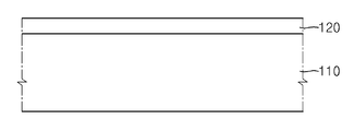
115...개구 120...마이크로포어층
125...마이크로포어 130...그래핀 시트
132...불활성영역 134...나노전극영역
141...제1전극 142...제2전극
151...제1 전극패드 152...제2 전극패드
210...수조 241...제3전극
242...제4전극
Claims (22)
- 삭제
- 삭제
- 삭제
- 삭제
- 삭제
- 삭제
- 삭제
- 삭제
- 삭제
- 삭제
- 삭제
- 삭제
- 삭제
- 삭제
- 기판 상에 절연물질로 이루어진 마이크로포어층을 형성하는 단계;
상기 마이크로포어층 상에 그래핀으로 이루어진 나노 전극을 형성하는 단계;
상기 마이크로포어층을 관통하는 마이크로포어(micropore)를 형성하는 단계; 및
상기 나노 전극을 관통하며 상기 마이크로포어와 마주하는 나노갭(nanoogap)을 형성하는 단계:를 포함하며,
상기 나노 전극을 형성하는 단계는
상기 마이크로포어층 상에 그래핀 시트를 형성하는 단계;
상기 그래핀 시트가 물리적으로는 수 마이크론 크기의 폭을 가지고 전기적으로는 나노 크기의 폭을 가지도록, 상기 그래핀 시트의 영역 중 일부 영역을 전기적으로 불활성화시키는 단계;를 포함하며,
상기 일부 영역을 전기적으로 불활성화시키는 단계는
상기 그래핀 시트 상에 금속층을 형성하는 단계;
상기 금속층을 소정의 나노 영역 및 상기 나노 영역 양단에 각각 연결되는 제1전극과 제2전극을 포함하는 형상으로 패터닝하여 상기 그래핀 시트상의 일부 영역을 노출시키는 단계;
상기 일부 영역을 표면 처리하여 불활성영역을 형성하는 단계;
상기 금속층에서 상기 나노 영역 부분을 식각하는 단계;를 포함하는, 나노갭 센서 제조방법. - 삭제
- 제15항에 있어서,
상기 표면 처리는 F, Cl, 또는 Br을 사용하는, 나노갭 센서 제조방법. - 제15항에 있어서,
상기 금속층을 패터닝할 때, 전자빔 리소그라피(electron beam lithography) 방법을 사용하는 나노갭 센서 제조방법. - 제15항에 있어서,
상기 금속층에서 상기 나노 영역 부분을 식각하는 단계 이전에,
상기 제1전극 및 제2전극에 각각 연결되는 제1 전극패드 및 제2 전극패드를 형성하는 단계;를 더 포함하는 나노갭 센서 제조방법. - 제15항에 있어서,
상기 금속층에서 상기 나노 영역 부분을 식각하는 단계 이전에,
상기 제1전극 및 제2전극에 각각 연결되는 제1 전극패드 및 제2 전극패드를 형성하는 단계;를 더 포함하는 나노갭 센서 제조방법. - 제20항에 있어서,
상기 제1 전극패드 및 제2 전극패드를 형성하는 단계에서 포토 리소그라피(photo lithography) 공정을 사용하는 나노갭 센서 제조방법. - 제15항에 있어서,
상기 나노갭을 형성하는 단계는
TEM(transmission electron microscope) 장비를 이용하는 나노갭 센서 제조방법.
Priority Applications (2)
| Application Number | Priority Date | Filing Date | Title |
|---|---|---|---|
| KR1020120035600A KR101906967B1 (ko) | 2012-04-05 | 2012-04-05 | 나노갭 센서 및 이의 제조 방법 |
| US13/605,711 US9068914B2 (en) | 2012-04-05 | 2012-09-06 | Nanogap sensor and method of manufacturing the same |
Applications Claiming Priority (1)
| Application Number | Priority Date | Filing Date | Title |
|---|---|---|---|
| KR1020120035600A KR101906967B1 (ko) | 2012-04-05 | 2012-04-05 | 나노갭 센서 및 이의 제조 방법 |
Publications (2)
| Publication Number | Publication Date |
|---|---|
| KR20130113206A KR20130113206A (ko) | 2013-10-15 |
| KR101906967B1 true KR101906967B1 (ko) | 2018-10-11 |
Family
ID=49291788
Family Applications (1)
| Application Number | Title | Priority Date | Filing Date |
|---|---|---|---|
| KR1020120035600A Active KR101906967B1 (ko) | 2012-04-05 | 2012-04-05 | 나노갭 센서 및 이의 제조 방법 |
Country Status (2)
| Country | Link |
|---|---|
| US (1) | US9068914B2 (ko) |
| KR (1) | KR101906967B1 (ko) |
Families Citing this family (18)
| Publication number | Priority date | Publication date | Assignee | Title |
|---|---|---|---|---|
| US8986524B2 (en) | 2011-01-28 | 2015-03-24 | International Business Machines Corporation | DNA sequence using multiple metal layer structure with different organic coatings forming different transient bondings to DNA |
| CN108051578B (zh) | 2011-04-04 | 2020-07-24 | 哈佛大学校长及研究员协会 | 通过局部电位测量进行的纳米孔感测 |
| US10029915B2 (en) | 2012-04-04 | 2018-07-24 | International Business Machines Corporation | Functionally switchable self-assembled coating compound for controlling translocation of molecule through nanopores |
| US9046511B2 (en) | 2013-04-18 | 2015-06-02 | International Business Machines Corporation | Fabrication of tunneling junction for nanopore DNA sequencing |
| US9182369B2 (en) | 2013-06-19 | 2015-11-10 | Globalfoundries Inc. | Manufacturable sub-3 nanometer palladium gap devices for fixed electrode tunneling recognition |
| US9188578B2 (en) | 2013-06-19 | 2015-11-17 | Globalfoundries Inc. | Nanogap device with capped nanowire structures |
| WO2015077751A1 (en) * | 2013-11-25 | 2015-05-28 | Northeastern University | Freestanding ultra thin membranes and transfer-free fabrication thereof |
| KR101489154B1 (ko) | 2014-06-26 | 2015-02-03 | 국민대학교산학협력단 | 잔류응력을 이용한 나노갭 센서의 제조방법 및 이에 의해 제조되는 나노갭 센서 |
| CN112816679B (zh) * | 2015-02-05 | 2024-05-28 | 哈佛大学校长及研究员协会 | 一种用于感测分子穿过纳米孔的移位的方法 |
| US11163022B2 (en) | 2015-06-12 | 2021-11-02 | Allegro Microsystems, Llc | Magnetic field sensor for angle detection with a phase-locked loop |
| CN108700542A (zh) * | 2015-12-14 | 2018-10-23 | 瓦伦汀·杜布瓦 | 裂纹结构、使用裂纹结构的隧穿结以及制作其的方法 |
| GB201610187D0 (en) * | 2016-06-10 | 2016-07-27 | Univ Leiden And Stichting Voor Fundamenteel Onderzoek Der Materie | Method |
| US10168299B2 (en) | 2016-07-15 | 2019-01-01 | International Business Machines Corporation | Reproducible and manufacturable nanogaps for embedded transverse electrode pairs in nanochannels |
| CN108470777B (zh) * | 2018-03-13 | 2020-01-07 | 华东师范大学 | 用于透射电镜原位通电芯片的拥有纳米级间距小电极的材料测试单元制备方法 |
| CN110797457B (zh) * | 2019-10-22 | 2021-10-12 | 华东师范大学 | 一种多层存储结构透射电子显微镜原位电学测试单元制备方法 |
| US12011715B2 (en) | 2020-11-11 | 2024-06-18 | International Business Machines Corporation | Tailorable electrode capping for microfluidic devices |
| US12090477B2 (en) * | 2021-03-05 | 2024-09-17 | Taiwan Semiconductor Manufacturing Company Ltd. | System and method for detecting biomolecules |
| CN119355091B (zh) * | 2024-12-27 | 2025-04-15 | 合肥美镓传感科技有限公司 | 气体传感器及其制备方法 |
Citations (3)
| Publication number | Priority date | Publication date | Assignee | Title |
|---|---|---|---|---|
| WO2009035647A1 (en) | 2007-09-12 | 2009-03-19 | President And Fellows Of Harvard College | High-resolution molecular graphene sensor comprising an aperture in the graphene layer |
| CN102095768A (zh) | 2010-11-16 | 2011-06-15 | 浙江大学 | 一种亚纳米厚度的纳米孔传感器 |
| US20120037919A1 (en) | 2009-10-22 | 2012-02-16 | Zhejian University | Nanopore electrical sensor |
Family Cites Families (20)
| Publication number | Priority date | Publication date | Assignee | Title |
|---|---|---|---|---|
| US7144486B1 (en) * | 1997-04-30 | 2006-12-05 | Board Of Trustees Of The University Of Arkansas | Multilayer microcavity devices and methods |
| US7258838B2 (en) | 1999-06-22 | 2007-08-21 | President And Fellows Of Harvard College | Solid state molecular probe device |
| US7582490B2 (en) | 1999-06-22 | 2009-09-01 | President And Fellows Of Harvard College | Controlled fabrication of gaps in electrically conducting structures |
| US6905586B2 (en) | 2002-01-28 | 2005-06-14 | Ut-Battelle, Llc | DNA and RNA sequencing by nanoscale reading through programmable electrophoresis and nanoelectrode-gated tunneling and dielectric detection |
| US20040043888A1 (en) * | 2002-08-28 | 2004-03-04 | Noritake Co., Limited | Compositions and methods for making microporous ceramic materials |
| US20040188780A1 (en) | 2003-03-25 | 2004-09-30 | Kurtz Anthony D. | Nanotube semiconductor structures with varying electrical properties |
| US8044472B2 (en) | 2003-03-25 | 2011-10-25 | Kulite Semiconductor Products, Inc. | Nanotube and graphene semiconductor structures with varying electrical properties |
| JP5025159B2 (ja) * | 2006-04-28 | 2012-09-12 | シスメックス株式会社 | 生体成分測定装置 |
| US7638034B2 (en) | 2006-09-21 | 2009-12-29 | Los Alamos National Security, Llc | Electrochemical detection of single molecules using abiotic nanopores having electrically tunable dimensions |
| WO2009131724A2 (en) | 2008-01-24 | 2009-10-29 | Massachusetts Institute Of Technology | Insulated nanogap devices and methods of use thereof |
| US8961757B2 (en) * | 2008-03-18 | 2015-02-24 | Arizona Board Of Regents, A Body Corporate Of The State Of Arizona Acting For And On Behalf Of Arizona State University | Nanopore and carbon nanotube based DNA sequencer |
| CN101960300B (zh) * | 2008-05-28 | 2013-05-29 | 松下电器产业株式会社 | 使用电化学测定装置检测或者定量目标物质的方法、电化学测定装置以及电化学测定用电极板 |
| WO2010022321A1 (en) * | 2008-08-21 | 2010-02-25 | Georgia Tech Research Corporation | Gas sensors, methods of preparation thereof, methods of selecting gas sensor materials, and methods of use of gas sensors |
| US8313633B2 (en) * | 2009-07-28 | 2012-11-20 | Polestar Technologies, Inc. | Molecular imprinted nanosensors and process for producing same |
| US8227842B2 (en) * | 2009-09-21 | 2012-07-24 | Hitachi Global Storage Technologies Netherlands B.V. | Quantum well graphene structure |
| KR101715355B1 (ko) * | 2010-11-30 | 2017-03-13 | 삼성전자주식회사 | 그래핀 전자 소자 |
| US20120141799A1 (en) * | 2010-12-03 | 2012-06-07 | Francis Kub | Film on Graphene on a Substrate and Method and Devices Therefor |
| US8585973B2 (en) * | 2011-05-27 | 2013-11-19 | The Board Of Trustees Of The Leland Stanford Junior University | Nano-sensor array |
| US8652805B2 (en) * | 2011-08-15 | 2014-02-18 | International Business Machines Corporation | Trapping molecular segments in nano-gaps |
| US8912525B2 (en) * | 2011-12-16 | 2014-12-16 | International Business Machines Corporation | Chemical oxidation of graphene and carbon nanotubes using Cerium (IV) ammonium nitrate |
-
2012
- 2012-04-05 KR KR1020120035600A patent/KR101906967B1/ko active Active
- 2012-09-06 US US13/605,711 patent/US9068914B2/en active Active
Patent Citations (3)
| Publication number | Priority date | Publication date | Assignee | Title |
|---|---|---|---|---|
| WO2009035647A1 (en) | 2007-09-12 | 2009-03-19 | President And Fellows Of Harvard College | High-resolution molecular graphene sensor comprising an aperture in the graphene layer |
| US20120037919A1 (en) | 2009-10-22 | 2012-02-16 | Zhejian University | Nanopore electrical sensor |
| CN102095768A (zh) | 2010-11-16 | 2011-06-15 | 浙江大学 | 一种亚纳米厚度的纳米孔传感器 |
Also Published As
| Publication number | Publication date |
|---|---|
| US9068914B2 (en) | 2015-06-30 |
| US20130265031A1 (en) | 2013-10-10 |
| KR20130113206A (ko) | 2013-10-15 |
Similar Documents
| Publication | Publication Date | Title |
|---|---|---|
| KR101906967B1 (ko) | 나노갭 센서 및 이의 제조 방법 | |
| KR102144995B1 (ko) | 그래핀 나노포어를 포함하는 나노포어 소자 및 그 제조 방법 | |
| KR101910978B1 (ko) | 나노 센서 및 그의 제조 방법 | |
| US7964143B2 (en) | Nanotube device and method of fabrication | |
| CN103890580B (zh) | 用于处理单分子的设备 | |
| US11810953B2 (en) | Sensor having graphene transistors | |
| US20150268191A1 (en) | Chemical sensing and/or measuring devices and methods | |
| EP1657539A1 (en) | Nanostructure resonant tunneling with a gate voltage source | |
| KR101403406B1 (ko) | 공중부유형 탄소 나노와이어 기반 가스센서 및 온도센서 제조방법 | |
| TW201322448A (zh) | 奈米網格通道鰭式場效電晶體及生物感測器 | |
| KR101878747B1 (ko) | 나노갭 소자 및 이로부터의 신호를 처리하는 방법 | |
| CN110050187B (zh) | 用于测量试样的小电位的设备、该设备的制造方法和应用 | |
| KR101987556B1 (ko) | 유연성 나노-포어 소자 및 이의 제조 방법 | |
| US8368123B2 (en) | Apparatus for sensing an event | |
| JP6568644B2 (ja) | メンブレンデバイスの製造方法、メンブレンデバイス、および、ナノポアデバイス | |
| CN117233234B (zh) | 一种基于氮化镓晶体管的生物分子传感器及其制作方法 | |
| US11322702B1 (en) | Electrical devices having radiofrequency field effect transistors and the manufacture thereof | |
| KR101927415B1 (ko) | 나노갭 소자 및 이로부터의 신호를 처리하는 방법 | |
| KR20140028602A (ko) | 그래핀을 포함하는 나노 센서 및 이의 제조 방법 | |
| KR100549227B1 (ko) | 유기분자 소자의 제작 방법 | |
| KR101163202B1 (ko) | 실리콘 나노와이어 소자 제조방법 | |
| KR100696870B1 (ko) | 양자점 트랜지스터 원자간력 현미경 캔틸레버 및 그 제조방법 | |
| KR20080052250A (ko) | 나노 와이어 배열 소자 제조방법 | |
| RU2539677C2 (ru) | Зонд на основе полевого транзистора с наноразмерным каналом | |
| KR20060000809A (ko) | 액체에서 사용가능한 고 종횡비 단전자 트랜지스터 구조를갖는 원자간력 현미경 캔틸레버 및 그 제조방법 |
Legal Events
| Date | Code | Title | Description |
|---|---|---|---|
| PA0109 | Patent application |
St.27 status event code: A-0-1-A10-A12-nap-PA0109 |
|
| R18-X000 | Changes to party contact information recorded |
St.27 status event code: A-3-3-R10-R18-oth-X000 |
|
| PG1501 | Laying open of application |
St.27 status event code: A-1-1-Q10-Q12-nap-PG1501 |
|
| A201 | Request for examination | ||
| PA0201 | Request for examination |
St.27 status event code: A-1-2-D10-D11-exm-PA0201 |
|
| D13-X000 | Search requested |
St.27 status event code: A-1-2-D10-D13-srh-X000 |
|
| D14-X000 | Search report completed |
St.27 status event code: A-1-2-D10-D14-srh-X000 |
|
| E902 | Notification of reason for refusal | ||
| PE0902 | Notice of grounds for rejection |
St.27 status event code: A-1-2-D10-D21-exm-PE0902 |
|
| AMND | Amendment | ||
| E13-X000 | Pre-grant limitation requested |
St.27 status event code: A-2-3-E10-E13-lim-X000 |
|
| P11-X000 | Amendment of application requested |
St.27 status event code: A-2-2-P10-P11-nap-X000 |
|
| P13-X000 | Application amended |
St.27 status event code: A-2-2-P10-P13-nap-X000 |
|
| E601 | Decision to refuse application | ||
| PE0601 | Decision on rejection of patent |
St.27 status event code: N-2-6-B10-B15-exm-PE0601 |
|
| X091 | Application refused [patent] | ||
| AMND | Amendment | ||
| E13-X000 | Pre-grant limitation requested |
St.27 status event code: A-2-3-E10-E13-lim-X000 |
|
| P11-X000 | Amendment of application requested |
St.27 status event code: A-2-2-P10-P11-nap-X000 |
|
| P13-X000 | Application amended |
St.27 status event code: A-2-2-P10-P13-nap-X000 |
|
| PX0901 | Re-examination |
St.27 status event code: A-2-3-E10-E12-rex-PX0901 |
|
| PX0701 | Decision of registration after re-examination |
St.27 status event code: A-3-4-F10-F13-rex-PX0701 |
|
| X701 | Decision to grant (after re-examination) | ||
| GRNT | Written decision to grant | ||
| PR0701 | Registration of establishment |
St.27 status event code: A-2-4-F10-F11-exm-PR0701 |
|
| PR1002 | Payment of registration fee |
St.27 status event code: A-2-2-U10-U11-oth-PR1002 Fee payment year number: 1 |
|
| PG1601 | Publication of registration |
St.27 status event code: A-4-4-Q10-Q13-nap-PG1601 |
|
| FPAY | Annual fee payment |
Payment date: 20210916 Year of fee payment: 4 |
|
| PR1001 | Payment of annual fee |
St.27 status event code: A-4-4-U10-U11-oth-PR1001 Fee payment year number: 4 |
|
| FPAY | Annual fee payment |
Payment date: 20220916 Year of fee payment: 5 |
|
| PR1001 | Payment of annual fee |
St.27 status event code: A-4-4-U10-U11-oth-PR1001 Fee payment year number: 5 |
|
| PR1001 | Payment of annual fee |
St.27 status event code: A-4-4-U10-U11-oth-PR1001 Fee payment year number: 6 |
|
| P22-X000 | Classification modified |
St.27 status event code: A-4-4-P10-P22-nap-X000 |
|
| PR1001 | Payment of annual fee |
St.27 status event code: A-4-4-U10-U11-oth-PR1001 Fee payment year number: 7 |
|
| PR1001 | Payment of annual fee |
St.27 status event code: A-4-4-U10-U11-oth-PR1001 Fee payment year number: 8 |
|
| U11 | Full renewal or maintenance fee paid |
Free format text: ST27 STATUS EVENT CODE: A-4-4-U10-U11-OTH-PR1001 (AS PROVIDED BY THE NATIONAL OFFICE) Year of fee payment: 8 |