KR101894598B1 - Plasma processing apparatus - Google Patents
Plasma processing apparatus Download PDFInfo
- Publication number
- KR101894598B1 KR101894598B1 KR1020120021927A KR20120021927A KR101894598B1 KR 101894598 B1 KR101894598 B1 KR 101894598B1 KR 1020120021927 A KR1020120021927 A KR 1020120021927A KR 20120021927 A KR20120021927 A KR 20120021927A KR 101894598 B1 KR101894598 B1 KR 101894598B1
- Authority
- KR
- South Korea
- Prior art keywords
- processing apparatus
- plasma processing
- plasma
- annular plates
- shower head
- Prior art date
- Legal status (The legal status is an assumption and is not a legal conclusion. Google has not performed a legal analysis and makes no representation as to the accuracy of the status listed.)
- Expired - Fee Related
Links
Images


Classifications
-
- H—ELECTRICITY
- H01—ELECTRIC ELEMENTS
- H01J—ELECTRIC DISCHARGE TUBES OR DISCHARGE LAMPS
- H01J37/00—Discharge tubes with provision for introducing objects or material to be exposed to the discharge, e.g. for the purpose of examination or processing thereof
- H01J37/32—Gas-filled discharge tubes
- H01J37/32431—Constructional details of the reactor
- H01J37/3244—Gas supply means
Landscapes
- Physics & Mathematics (AREA)
- Engineering & Computer Science (AREA)
- Plasma & Fusion (AREA)
- Chemical & Material Sciences (AREA)
- Analytical Chemistry (AREA)
- Drying Of Semiconductors (AREA)
- Plasma Technology (AREA)
Abstract
본 발명은 종래에 비해서 보다 미세한 플라즈마 제어를 가능하게 할 수 있는 플라즈마 처리 장치를 제공한다.
내부에서 기판을 처리하는 처리 챔버에, 기판을 배치하기 위한 배치대와 대향하도록 설치되고, 배치대와 대향하는 대향면에 복수 마련된 가스 토출 구멍을 통하여 기판을 향해서 가스를 샤워형으로 공급하는 샤워 헤드를 구비한 플라즈마 처리 장치로서, 샤워 헤드의 대향면과 반대측의 면을 관통하는 복수의 배기 구멍과, 반대측의 면측의 배기 구멍과 연통하는 배기 공간 내에, 반대측의 면과 평행하게 배치되고, 도전성 재료로 이루어지는 환상의 판체와, 판체를 이동시켜 배기 구멍과의 거리를 변경하기 위한 이동 수단을 구비하고 있다. The present invention provides a plasma processing apparatus capable of enabling finer plasma control than conventional plasma processing apparatuses.
A shower head which is provided so as to face a stage for placing a substrate in a processing chamber for treating the substrate inside and which supplies gas in a shower shape toward the substrate through a plurality of gas discharging holes provided on opposed surfaces opposed to the stage, The plasma processing apparatus is provided with a plurality of exhaust holes passing through a surface opposite to the opposite surface of a shower head and an exhaust space communicating with an exhaust hole on an opposite surface side, And a moving means for moving the plate body to change the distance between the plate body and the exhaust hole.
Description
본 발명은, 플라즈마 처리 장치에 관한 것이다. The present invention relates to a plasma processing apparatus.
종래부터, 반도체 장치의 제조 분야 등에 있어서는, 반도체 웨이퍼 등의 기판에 플라즈마를 작용시켜 에칭 처리나 성막 처리를 실시하는 플라즈마 처리 장치가 이용되고 있다. 2. Description of the Related Art Conventionally, in the field of manufacturing semiconductor devices and the like, a plasma processing apparatus for performing etching treatment or film forming treatment by applying a plasma to a substrate such as a semiconductor wafer is used.
이러한 플라즈마 처리 장치에서는, 처리 챔버의 주위에 설치한 자석에 의해서 처리 공간 내에 자장을 형성하여, 처리 공간 내의 플라즈마를 제어하는 것이 알려져 있다(예컨대, 특허문헌 1 참조). 또한, 처리 챔버로부터 배기하는 부위에 자석에 의해서 자장을 형성하여, 가스의 통과를 허용하면서 플라즈마의 통과를 저지하여 플라즈마를 처리 공간 내에 가두는 기술이 알려져 있다(예컨대, 특허문헌 2 참조). In such a plasma processing apparatus, it is known that a magnetic field is formed in a processing space by a magnet provided around a processing chamber to control plasma in the processing space (see, for example, Patent Document 1). Further, there is known a technique in which a magnetic field is formed by a magnet at a portion to be exhausted from a processing chamber to block the passage of plasma while permitting passage of the gas, thereby confining the plasma in the processing space (see, for example, Patent Document 2).
전술한 바와 같이, 종래의 플라즈마 처리 장치에서는, 처리 공간 내에 형성한 자장에 의해서 플라즈마를 제어하거나, 플라즈마를 가두는 것이 실행되고 있다. As described above, in the conventional plasma processing apparatus, the plasma is controlled by the magnetic field formed in the processing space or the plasma is confined.
그러나 반도체 장치의 제조 분야에서는, 최근 다층막 구조의 일괄 에칭이 주류가 되고 있기 때문에, 하나의 처리 챔버 내에서 복수의 공정을 실시할 필요성이 있다. 이 때문에, 개개의 프로세스 조건에 맞는 보다 미세한 플라즈마 제어를 가능하게 하는 것이 요구되고 있다. However, in the field of manufacturing semiconductor devices, since batch etching of multi-layer film structures has become mainstream in recent years, it is necessary to perform a plurality of processes in one processing chamber. For this reason, it is required to enable finer plasma control suited to individual process conditions.
본 발명은, 상기 종래의 사정을 감안하여 이루어진 것으로, 종래에 비해서 보다 미세한 플라즈마 제어를 가능하게 하는 플라즈마 처리 장치를 제공하기 위한 것이다. SUMMARY OF THE INVENTION The present invention has been made in view of the above-described conventional circumstances, and it is an object of the present invention to provide a plasma processing apparatus capable of finer plasma control than the prior art.
본 발명에 따른 플라즈마 처리 장치는, 내부에서 기판을 처리하는 처리 챔버에, 상기 기판을 배치하기 위한 배치대와 대향하도록 마련되고, 상기 배치대와 대향하는 대향면에 복수 마련된 가스 토출 구멍으로부터 상기 기판을 향해서 가스를 샤워형으로 공급하는 샤워 헤드를 구비한 플라즈마 처리 장치로서, 상기 샤워 헤드의 상기 대향면과 반대측의 면을 관통하는 복수의 배기 구멍과, 상기 반대측의 면측의 상기 배기 구멍과 연통하는 배기 공간 내에 상기 반대측의 면과 평행하게 배치되며, 도전성 재료로 이루어지는 환상의 판체와, 상기 판체를 이동시켜 상기 배기 구멍과의 거리를 변경하기 위한 이동 수단을 구비하는 것을 특징으로 한다. A plasma processing apparatus according to the present invention is a plasma processing apparatus comprising a processing chamber for processing a substrate therein, and a plurality of gas discharge holes provided in opposing faces of the processing chamber facing the arrangement stand for arranging the substrate, A plurality of exhaust holes passing through a surface of the shower head opposite to the facing surface of the shower head and a plurality of exhaust holes communicating with the exhaust holes on the surface of the opposite side of the shower head, An annular plate member disposed in the exhaust space in parallel with the surface on the opposite side and made of a conductive material and a moving means for moving the plate member to change the distance between the exhaust hole and the exhaust hole.
본 발명에 따르면, 종래에 비해서 보다 미세한 플라즈마 제어를 가능하게 할 수 있는 플라즈마 처리 장치를 제공할 수 있다. According to the present invention, it is possible to provide a plasma processing apparatus capable of performing finer plasma control as compared with the conventional plasma processing apparatus.
도 1은 본 발명의 일 실시형태에 따른 플라즈마 처리 장치의 구성을 모식적으로 도시하는 종단면도이다.
도 2는 도 1의 플라즈마 처리 장치의 주요부 구성을 모식적으로 도시하는 도면이다.
도 3은 도 1의 플라즈마 처리 장치의 주요부 구성을 모식적으로 도시하는 도면이다. 1 is a longitudinal sectional view schematically showing a configuration of a plasma processing apparatus according to an embodiment of the present invention.
Fig. 2 is a diagram schematically showing the configuration of main parts of the plasma processing apparatus of Fig. 1;
Fig. 3 is a diagram schematically showing the configuration of the main part of the plasma processing apparatus of Fig. 1. Fig.
이하, 도면을 참조하여, 본 발명의 실시형태에 대해서 상세하게 설명한다. Hereinafter, embodiments of the present invention will be described in detail with reference to the drawings.
도 1은, 본 발명의 플라즈마 처리 장치의 일 실시형태에 따른 플라즈마 에칭 장치(200)의 단면 구성을 모식적으로 도시하는 것이다. 1 schematically shows a sectional configuration of a
도 1에 도시한 바와 같이, 플라즈마 에칭 장치(200)는, 예컨대 표면이 양극 산화처리된 알루미늄 등으로 이루어지고 원통 형상으로 형성된 처리 챔버(처리 용기; 201)를 구비하고, 이 처리 챔버(201)는 접지되어 있다. 처리 챔버(201) 내에는, 피처리 기판으로서의 반도체 웨이퍼를 배치하고, 또한 하부 전극을 구성하는 배치대(202)가 설치된다. 이 배치대(202)에는, 하나 또는 복수의 도시하지 않는 플라즈마 형성용 전원이 접속되어 있다. 1, the
배치대(202)의 상측에는, 그 위에 반도체 웨이퍼를 정전 흡착하기 위한 정전척(203)이 설치된다. 정전척(203)은, 절연재의 사이에 전극을 배치함으로써 구성되며, 이 전극에 직류 전압을 인가함으로써, 쿨롱력에 의해서 반도체 웨이퍼를 정전 흡착한다. 또한, 배치대(202)에는, 온도 조절 매체를 순환시키기 위한 유로(204)가 형성되어, 정전척(203) 상에 흡착된 반도체 웨이퍼를 소정의 온도로 온도 조정할 수 있게 되어 있다. 또한, 처리 챔버(201)의 측벽부에는, 반도체 웨이퍼를 처리 챔버(201) 내에 반입, 반출하기 위한 개구(205)가 형성되어 있고, 여기에는, 개구(205)를 기밀하게 폐색하기 위한 개폐 기구(206)가 설치된다. An
배치대(202)의 상측에, 배치대(202)와 소정 간격을 두고 대향하도록, 샤워 헤드(100)가 배치되어 있다. 그리고 샤워 헤드(100)가 상부 전극으로 되고, 배치대(202)가 하부 전극으로 되는 한 쌍의 대향 전극이 형성되어 있다. A
도 2에 도시한 바와 같이, 샤워 헤드(100)는, 하측 부재(1)와, 이 하측 부재(1)의 상측에 배치된 상측 부재(2)의 2장의 판형 부재를 적층시킨 적층체(10)로 구성되어 있다. 이들 하측 부재(1) 및 상측 부재(2)는, 예컨대, 표면에 양극 산화처리를 한 알루미늄 등으로 구성되어 있다. 2, the
적층체(10) 중, 배치대(202)와 대향하는 대향면(14)을 형성하는 하측 부재(1)에는, 가스 토출 구멍(11)이 다수 형성되어 있고, 하측 부재(1)와 상측 부재(2)의 사이에는, 이들 가스 토출 구멍(11)에 연통하는 가스 유로(12)가 형성되어 있다. 이들 가스 토출 구멍(11)은, 도 1, 도 2에 화살표로 나타낸 바와 같이, 기판(도 1, 도 2의 하측)을 향해서 가스를 샤워형으로 공급하기 위한 것이다. 또한, 적층체(10)의 주연부에는, 가스 유로(12) 내에 가스를 도입하기 위한 가스 도입부(12a)가 설치된다. A plurality of
또한, 적층체(10)에는, 이 적층체(10), 즉 하측 부재(1)와 상측 부재(2)를 관통하여 배기 구멍(13)이 다수 형성되어 있다. 이들 배기 구멍(13)은, 도 1, 도 2에 점선의 화살표로 나타낸 바와 같이, 기판측(도면 중 하측)으로부터 기판과 반대측(도면 중 상측)을 향해서 가스의 흐름이 형성되도록 배기를 행하는 배기 기구를 구성하고 있다. 배기 구멍(13)은, 도 2에 도시하는 하측 부재(1) 부분에 형성된 세경(細徑) 부분(13a)의 직경이 예컨대 0.5∼1.5 mm 정도로 되어 있고, 상측 부재(2) 부분에 형성된 대경 부분(13b)의 직경이 예컨대 2.0∼5.0 mm 정도로 되어 있다. A plurality of
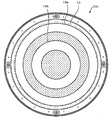
도 3은, 샤워 헤드(100)를 상측으로부터 본 평면 구성을 나타내고 있다. 도 3에 도시한 바와 같이, 배기 구멍(13)은, 샤워 헤드(100)의 주연부[처리 챔버(201)에 고정하기 위한 고정부로 됨)를 제외하고, 그 전체 영역에 걸쳐 대략 균등하게 설치된다. 배기 구멍(13)의 수는, 예컨대 12인치(300 mm) 직경의 반도체 웨이퍼를 처리하기 위한 샤워 헤드(100)의 경우, 2000∼2500개 정도이다. 또한, 도 3에 도시한 바와 같이, 본 실시형태에서는, 샤워 헤드(100)의 외형은, 피처리 기판인 반도체 웨이퍼의 외형에 맞추어 원판형으로 구성되어 있다. 또한, 도 3에 도시한 바와 같이, 샤워 헤드(100)의 상측에는, 후술하는 판체(16a) 및 판체(16b)가 배치되어 있다. Fig. 3 shows a plan view of the
도 1에 도시한 바와 같이, 샤워 헤드(100)의 가스 도입부(12a)는, 처리 챔버(201)에 설치된 가스 공급부(207)에 접속되어 있다. 가스 공급부(207)에는, 도시하지 않는 가스 공급 기구로부터 소정의 처리 가스(에칭 가스)가 공급된다. 1, the
또한, 샤워 헤드(100)의 상부에는, 통형상체(210)가 설치되어 있고, 이 통형상체(210)에는, 개폐 제어 밸브 및 개폐 기구 등을 통해 터보 분자 펌프 등의 진공 펌프(도시 생략)가 접속되어 있다. 이와 같이, 통형상체(210)의 내측이 배기로가 되고, 이 통형상체(210)의 내측의 배기로 내에, 도전성 재료[예컨대, 실리콘, 탄화규소, 알루미늄의 무구재)로 환상으로 형성된 복수(본 실시형태에서는 2개)의 판체(16a) 및 판체(16b)가 샤워 헤드(100)의 이면[15; 배치대(202)와 대향하는 대향면(14)과는 반대측의 면]과 대향하도록 배치되어 있다. 이들 판체(16a) 및 판체(16b)는, 도 3에 도시한 바와 같이 동심형으로 배치되어 있다. A
샤워 헤드(100)의 주연부에 위치하도록 설치된 판체(16a)는, 연결 부재(17a)를 통해 도 1의 좌측에 표시되는 구동 기구(161a)에 접속되어 있다. 그리고 판체(16a)는, 이 구동 기구(161a)에 의해서 판체(16b)와는 독립적으로 상하 이동 가능하게 되어 있다. The
한편, 판체(16a)보다 중앙부에 설치된 판체(16b)는, 연결 부재(17b)를 통해, 도 1의 우측에 표시되는 구동 기구(161b)에 접속되어 있다. 그리고 판체(16b)는, 이 구동 기구(161b)에 의해서 판체(16a)와는 독립적으로 상하 이동 가능하게 되어 있다. On the other hand, the
또한, 판체(16a)에는 전환 스위치(18a)가 전기적으로 접속되고, 판체(16b)에는 전환 스위치(18b)가 전기적으로 접속되어 있다. 이들 전환 스위치(18a) 및 전환 스위치(18b)에 의해서, 판체(16a) 및 판체(16b)를 전기적으로 접지된 상태와, 부유 상태(플로우팅 상태)로 설정할 수 있게 되어 있다. The
상기한 바와 같이 판체(16a) 및 판체(16b)는, 구동 기구(161a) 및 구동 기구(161b)에 의해서 상하 이동하여, 샤워 헤드(100)의 배기 구멍(13)과의 사이의 거리를 조절할 수 있게 되어 있다. 또한, 전환 스위치(18a) 및 전환 스위치(18b)에 의해서 전기적인 상태를, 접지 상태와 부유 상태(플로우팅 상태)로 설정할 수 있게 되어 있다. 이것에 의해서, 처리 챔버(201) 내의 샤워 헤드(100)와 배치대(202) 사의 처리 공간 내에서, 샤워 헤드(100)의 이면(15)측의 배기 공간으로의 플라즈마의 누설 상태를 조정할 수 있다. The
즉, 예컨대, 판체(16a) 및 판체(16b)를, 도 1의 하측에 위치시켜 배기 구멍(13)에 근접시킨 때는, 물리적 및 전기적으로 배기 구멍(13)으로부터의 플라즈마의 누설이 억제된 상태로 된다. 한편, 판체(16a) 및 판체(16b)를, 도 1의 상측에 위치시켜 배기 구멍(13)으로부터 이격시킨 때는, 배기 구멍(13)으로부터의 플라즈마의 누설이 보다 허용되는 상태로 된다. 또한, 판체(16a) 및 판체(16b)와 배기 구멍(13) 사이의 거리가 멀어질수록, 플라즈마의 누설 영역이 확대되도록 플라즈마의 상태를 제어할 수 있다. That is, for example, when the
또한, 예컨대 판체(16a)를 도 1의 상측에 위치시켜 배기 구멍(13)으로부터 이격시키고, 판체(16b)를 도 1의 하측에 위치시켜 배기 구멍(13)에 근접시킨 때는, 샤워 헤드(100)의 중앙부에서는 플라즈마의 누설이 억제된 상태로 되고, 샤워 헤드(100)의 주연부에서는 플라즈마의 누설이 허용된 상태로 된다. 이것에 의해서, 중앙부와 주연부에서 각각 부분적으로 플라즈마 밀도 등의 플라즈마의 상태를 제어할 수 있다. 1, for example, when the
예컨대, 처리 공간에서의 주연부의 플라즈마 밀도 등은, 중앙부에 비해서 저하되는 경향이 있는 경우가 많다. 이러한 경우, 예컨대, 주연부에서의 플라즈마의 누설을 생기게 하고, 중앙부에서의 플라즈마의 누설을 생기지 않도록 하면, 처리 공간 내의 중앙부의 전자나 이온이 주연부 방향으로 이동하여, 처리 공간 내에서의 플라즈마 밀도 등의 균일화를 도모할 수 있다. For example, the plasma density at the peripheral portion in the processing space tends to be lower than that at the central portion. In this case, for example, when plasma is leaked at the periphery and plasma leakage does not occur at the central portion, electrons and ions in the central portion in the processing space move in the peripheral direction and plasma density in the processing space So that uniformity can be achieved.
또한, 플라즈마를 제어하기 위하여, 처리 공간 내의 플라즈마에 직류 전압을 인가하는 경우, 예컨대, 처리 공간 내에 직류 전극을 배치하고 이 직류 전극에 직류 전압을 인가한 경우는, 판체(16a) 및 판체(16b)를 접지 전위에 접속하여, 직류 전압에 대한 접지 전극으로서 작용시킬 수도 있다. When a direct current voltage is applied to the plasma in the processing space to control the plasma, for example, when a direct current electrode is disposed in the processing space and a direct current voltage is applied to the direct current electrode, the
플라즈마 에칭 장치(200)에 의해서, 반도체 웨이퍼의 플라즈마 에칭을 행하는 경우에, 우선, 반도체 웨이퍼가 개구(205)로부터 처리 챔버(201) 내로 반입되어, 정전척(203) 상에 배치된다. 그리고 반도체 웨이퍼가 정전척(203) 상에 정전 흡착된다. 계속해서, 개구(205)가 폐쇄되고, 진공 펌프 등에 의해서, 처리 챔버(201)의 내부가 소정의 진공도까지 진공 상태로 된다. The semiconductor wafer is first brought into the
그 후, 소정 유량의 소정의 처리 가스(에칭 가스)가, 가스 공급부(207)로부터 샤워 헤드(100)의 가스 도입부(12a)에 공급되고, 이 처리 가스는, 샤워 헤드(100)의 가스 유로(12)를 지나서 가스 토출 구멍(11)을 통하여 샤워형으로 배치대(202) 상의 반도체 웨이퍼에 공급된다. Thereafter, a predetermined process gas (etching gas) at a predetermined flow rate is supplied from the
그리고 처리 챔버(201) 내의 압력이, 소정의 압력으로 유지된 후, 배치대(202)에 플라즈마 생성용의 높은 주파수의 고주파 전력으로서, 예컨대 40 MHz의 고주파 전력이 인가된다. 이에 따라, 상부 전극으로서의 샤워 헤드(100)와 하부 전극으로서의 배치대(202)의 사이에 고주파 전계가 생겨, 에칭 가스가 해리되어 플라즈마화 한다. 또한, 이와 동시에, 이온 인입용(바이어스용)의 낮은 주파수의 고주파 전력으로서, 예컨대 3.2 MHz의 고주파 전력이 배치대(202)에 인가된다. 이것에 의해서, 플라즈마로부터 인출된 이온 등에 의해서, 반도체 웨이퍼에 소정의 에칭 처리가 행해진다. After the pressure in the
상기 에칭 처리에 있어서, 샤워 헤드(100)의 가스 토출 구멍(11)을 통하여 샤워형으로 공급된 처리 가스는, 샤워 헤드(100)에 분산되어 다수 형성된 배기 구멍(13)을 통하여 배기되기 때문에, 처리 챔버(201)의 하부로부터 배기하는 경우와 같이, 반도체 웨이퍼의 중앙부로부터 주변부를 향하는 가스의 흐름이 형성되는 일이 없다. 이 때문에, 반도체 웨이퍼에 공급되는 처리 가스를 보다 균일화할 수 있다. Since the processing gas supplied in the form of a shower through the
또한, 전술한 바와 같이, 판체(16a) 및 판체(16b)의 위치의 조정과, 전기적인 상태의 변경에 의해서, 처리 챔버(201)의 처리 공간 내의 플라즈마를, 통형상체(210)의 내측의 배기 공간 내에 누설시키지 않도록 하여, 또는 통형상체(210)의 내측의 배기 공간 내에 누설시킴으로써, 처리 공간 내의 플라즈마의 상태를 제어할 수 있다. 이것에 의해서, 처리 공간 내의 플라즈마를 균일화할 수 있어, 반도체 웨이퍼의 각 부분에 균일한 에칭 처리를 실시할 수 있다. 즉, 처리의 면내 균일성을 향상시킬 수 있다. As described above, the plasma in the processing space of the
이러한 플라즈마의 제어는, 처리 챔버(201) 내의 플라즈마의 상태를 계측하는 계측 수단, 예컨대, 플라즈마의 발광 상태로부터 플라즈마의 상태를 검지하는 플라즈마 모니터에 의한 계측 결과에 기초하여, 구동 기구(161a, 161b)에 의한 판체(16a) 및 판체(16b)의 이동과, 전환 스위치(18a) 및 전환 스위치(18b)의 전환을 제어하는 제어 기구를 설치함으로써, 자동적으로 행할 수도 있다. This control of the plasma is performed by driving
그리고, 소정의 플라즈마 에칭 처리가 종료하면, 고주파 전력의 인가 및 처리 가스의 공급이 정지되어, 전술한 순서와는 역의 순서로, 반도체 웨이퍼가 처리 챔버(201) 내로부터 반출된다. When the predetermined plasma etching process is completed, the application of the high-frequency power and the supply of the process gas are stopped, and the semiconductor wafer is taken out from the
이상 설명한 바와 같이, 본 실시형태의 플라즈마 에칭 장치(200)에 따르면, 처리 공간 내의 플라즈마의 상태를, 프로세스 조건에 의해서 보다 미세하게 제어할 수 있다. As described above, according to the
또한, 상기 플라즈마 에칭 장치(200)에서는, 샤워 헤드(100)에 설치한 배기 구멍(13)을 통하여 배기를 하기 때문에, 종래의 장치와 같이, 배치대(202)의 주위 또는 샤워 헤드(100)의 주위에 배기 경로를 마련할 필요가 없다. 이 때문에, 처리 챔버(201)의 직경을 피처리 기판인 반도체 웨이퍼의 외경에 보다 근접시킬 수 있어, 장치의 소형화를 꾀할 수 있다. 또한, 진공 펌프를 처리 챔버(201)의 상측에 설치하고, 처리 챔버(201)의 처리 공간에 보다 가까운 부분으로부터 배기하기 때문에, 효율적으로 배기할 수 있어, 진공 펌프의 용량을 적게 하여 더욱 소형화를 꾀할 수 있다. Since the
이상, 본 발명을, 실시형태에 관해서 설명했지만, 본 발명은 이러한 실시형태로 한정되지 않으며, 물론 각종의 변형이 가능하다. 예컨대, 상기 실시형태에서는, 2개의 판체(16a) 및 판체(16b)를 배치한 예에 관해서 설명했지만, 판체의 수는 2개로 한정되지 않고, 몇 개라도 좋으며, 판체의 형상도 환상의 것으로 한정되지 않는다. Although the present invention has been described in connection with the embodiments, the present invention is not limited to these embodiments, and various modifications are possible. For example, in the above-described embodiment, the two
11 …… 가스 토출 구멍, 13 …… 배기 구멍, 16a, 16b…… 판체, 17a, 17b…… 연결 부재, 18a, 18b…… 전환 스위치, 100 …… 샤워 헤드, 161a, 161b……구동 기구, 200 ……플라즈마 에칭 장치, 201…… 처리 챔버, 202 …… 배치대. 11 ... ... Gas discharge hole, 13 ... ...
Claims (12)
기판을 배치하기 위한 배치대와 대향하도록 처리 챔버 내에 설치되고, 상기 배치대와 대향하는 대향면 상에 마련된 복수의 가스 토출 구멍으로부터 상기 기판을 향해서 가스를 샤워형으로 공급하는 샤워 헤드;
상기 샤워 헤드의 상기 대향면의 반대측에 위치된 반대측의 면을 관통하는 복수의 배기 구멍;
관통 구멍을 각각 갖지 않고, 상기 샤워 헤드의 상기 반대측의 면에 분포된 상기 복수의 배기 구멍과 연통하는 배기 공간 내에서 상기 샤워 헤드의 상기 반대측의 면과 평행하게 상기 샤워 헤드 위에 배치되며, 도전성 재료로 이루어지는 복수의 환상의 판체; 및
상기 복수의 환상의 판체를 각각 독립적으로 이동시켜, 상기 복수의 환상의 판체 중 하나 이상이 상기 배기 구멍에 근접하거나 또는 상기 배기 구멍으로부터 이격되도록 상기 복수의 환상의 판체 각각과 상기 배기 구멍 사이의 거리를 변화시킴으로써, 상기 샤워 헤드와 상기 배치대 사이의 상기 처리 챔버 내에 설치된 처리 공간으로부터 상기 샤워 헤드의 상기 반대측의 면 상에 마련된 상기 배기 공간을 향해서 플라즈마의 누설 상태를 억제 또는 허용하는 복수의 이동 수단
을 포함하고,
평평한 상부 표면 및 평평한 하부 표면을 각각 갖는 상기 복수의 환상의 판체는 상기 샤워 헤드의 반경 방향의 간극을 사이에 두고 미리 정해진 간격으로 동심형으로 배치되고, 상기 복수의 환상의 판체 각각은 상기 복수의 이동 수단에 각각 연결되는 것인 플라즈마 처리 장치.In the plasma processing apparatus,
A shower head which is provided in the processing chamber so as to face a placement stand for arranging the substrate and supplies the gas from the plurality of gas discharge holes provided on the facing surface opposing the placement stand toward the substrate in a shower;
A plurality of exhaust holes passing through a surface on the opposite side of the shower head opposite to the opposed surface;
And is disposed on the shower head in parallel with the opposite surface of the shower head in an exhaust space communicating with the plurality of exhaust holes distributed on the opposite surface of the shower head, A plurality of annular plates; And
And a distance between each of the plurality of annular plates and the exhaust hole so that at least one of the plurality of annular plates is adjacent to or spaced from the exhaust hole, A plurality of moving means for suppressing or permitting the leakage of the plasma from the processing space provided in the processing chamber between the showerhead and the placement table to the exhaust space provided on the opposite side of the showerhead,
/ RTI >
The plurality of annular plates each having a flat upper surface and a flat lower surface are concentrically arranged at a predetermined interval with a gap in the radial direction of the shower head interposed therebetween, Wherein the plasma processing apparatus is connected to the transfer means.
직류 전압이 상기 직류 전극에 인가되며,
상기 환상의 판체 각각은, 접지 전위에 접속되어 상기 직류 전압에 대한 접지 전극으로서 작용하도록 구성되는 것인 플라즈마 처리 장치.The plasma processing apparatus according to claim 1, further comprising a DC electrode disposed in the processing space of the processing chamber,
A direct current voltage is applied to the direct current electrode,
Wherein each of the annular plates is configured to be connected to a ground potential and to serve as a ground electrode for the DC voltage.
Applications Claiming Priority (2)
| Application Number | Priority Date | Filing Date | Title |
|---|---|---|---|
| JPJP-P-2011-046769 | 2011-03-03 | ||
| JP2011046769A JP5661513B2 (en) | 2011-03-03 | 2011-03-03 | Plasma processing equipment |
Publications (2)
| Publication Number | Publication Date |
|---|---|
| KR20120100815A KR20120100815A (en) | 2012-09-12 |
| KR101894598B1 true KR101894598B1 (en) | 2018-09-03 |
Family
ID=46752555
Family Applications (1)
| Application Number | Title | Priority Date | Filing Date |
|---|---|---|---|
| KR1020120021927A Expired - Fee Related KR101894598B1 (en) | 2011-03-03 | 2012-03-02 | Plasma processing apparatus |
Country Status (3)
| Country | Link |
|---|---|
| US (1) | US9589771B2 (en) |
| JP (1) | JP5661513B2 (en) |
| KR (1) | KR101894598B1 (en) |
Families Citing this family (2)
| Publication number | Priority date | Publication date | Assignee | Title |
|---|---|---|---|---|
| JP5444044B2 (en) * | 2010-03-02 | 2014-03-19 | 東京エレクトロン株式会社 | Plasma processing apparatus and shower head |
| JP6570993B2 (en) * | 2015-12-16 | 2019-09-04 | 東京エレクトロン株式会社 | Plasma processing equipment |
Citations (3)
| Publication number | Priority date | Publication date | Assignee | Title |
|---|---|---|---|---|
| US20020003126A1 (en) | 1999-04-13 | 2002-01-10 | Ajay Kumar | Method of etching silicon nitride |
| US20030227258A1 (en) * | 2000-08-10 | 2003-12-11 | Strang Eric J. | Method and apparatus for tuning a plasma reactor chamber |
| US20090236041A1 (en) * | 2008-03-19 | 2009-09-24 | Tokyo Electron Limited | Shower head and substrate processing apparatus |
Family Cites Families (15)
| Publication number | Priority date | Publication date | Assignee | Title |
|---|---|---|---|---|
| US4590042A (en) * | 1984-12-24 | 1986-05-20 | Tegal Corporation | Plasma reactor having slotted manifold |
| JPH0649645A (en) * | 1992-07-31 | 1994-02-22 | Yoshida Kogyo Kk <Ykk> | Hard multilayer film forming body and method for producing the same |
| US6322661B1 (en) * | 1999-11-15 | 2001-11-27 | Lam Research Corporation | Method and apparatus for controlling the volume of a plasma |
| US6261408B1 (en) * | 2000-02-16 | 2001-07-17 | Applied Materials, Inc. | Method and apparatus for semiconductor processing chamber pressure control |
| JP4009087B2 (en) | 2001-07-06 | 2007-11-14 | アプライド マテリアルズ インコーポレイテッド | Magnetic generator in semiconductor manufacturing apparatus, semiconductor manufacturing apparatus, and magnetic field intensity control method |
| JP2004235215A (en) * | 2003-01-28 | 2004-08-19 | Advanced Lcd Technologies Development Center Co Ltd | Plasma processing apparatus, plasma oxidation processing apparatus, and plasma processing method |
| JP4255747B2 (en) * | 2003-05-13 | 2009-04-15 | 東京エレクトロン株式会社 | Plasma processing apparatus and plasma processing method |
| US20070266945A1 (en) * | 2006-05-16 | 2007-11-22 | Asm Japan K.K. | Plasma cvd apparatus equipped with plasma blocking insulation plate |
| JP5154124B2 (en) * | 2007-03-29 | 2013-02-27 | 東京エレクトロン株式会社 | Plasma processing equipment |
| JP2009044075A (en) * | 2007-08-10 | 2009-02-26 | Toshiba Corp | Plasma processing apparatus and plasma etching method |
| KR101470865B1 (en) * | 2008-02-15 | 2014-12-10 | 엘아이지에이디피 주식회사 | Plasma processing apparatus for control of baffle opening volume |
| JP5248370B2 (en) * | 2009-03-10 | 2013-07-31 | 東京エレクトロン株式会社 | Shower head and plasma processing apparatus |
| JP5350043B2 (en) * | 2009-03-31 | 2013-11-27 | 東京エレクトロン株式会社 | Plasma processing apparatus and plasma processing method |
| JP5597463B2 (en) * | 2010-07-05 | 2014-10-01 | 東京エレクトロン株式会社 | Substrate processing apparatus and substrate processing method |
| US9184028B2 (en) * | 2010-08-04 | 2015-11-10 | Lam Research Corporation | Dual plasma volume processing apparatus for neutral/ion flux control |
-
2011
- 2011-03-03 JP JP2011046769A patent/JP5661513B2/en not_active Expired - Fee Related
-
2012
- 2012-03-02 US US13/410,994 patent/US9589771B2/en not_active Expired - Fee Related
- 2012-03-02 KR KR1020120021927A patent/KR101894598B1/en not_active Expired - Fee Related
Patent Citations (3)
| Publication number | Priority date | Publication date | Assignee | Title |
|---|---|---|---|---|
| US20020003126A1 (en) | 1999-04-13 | 2002-01-10 | Ajay Kumar | Method of etching silicon nitride |
| US20030227258A1 (en) * | 2000-08-10 | 2003-12-11 | Strang Eric J. | Method and apparatus for tuning a plasma reactor chamber |
| US20090236041A1 (en) * | 2008-03-19 | 2009-09-24 | Tokyo Electron Limited | Shower head and substrate processing apparatus |
Also Published As
| Publication number | Publication date |
|---|---|
| JP2012186223A (en) | 2012-09-27 |
| JP5661513B2 (en) | 2015-01-28 |
| US9589771B2 (en) | 2017-03-07 |
| US20120222814A1 (en) | 2012-09-06 |
| KR20120100815A (en) | 2012-09-12 |
Similar Documents
| Publication | Publication Date | Title |
|---|---|---|
| KR102582878B1 (en) | Electrostatic chucking method and substrate processing apparatus | |
| KR101672856B1 (en) | Plasma processing apparatus | |
| KR101731017B1 (en) | Substrate for electrostatic chuck and electrostatic chuck | |
| US9055661B2 (en) | Plasma processing apparatus | |
| US8366828B2 (en) | Shower head and substrate processing apparatus | |
| JP3210207B2 (en) | Plasma processing equipment | |
| US8747609B2 (en) | Plasma processing apparatus and shower head | |
| KR101850355B1 (en) | Plasma processing apparatus | |
| JP5248370B2 (en) | Shower head and plasma processing apparatus | |
| US20130014895A1 (en) | Substrate processing apparatus | |
| US20070215279A1 (en) | Plasma processing apparatus, plasma processing method, focus ring, and focus ring component | |
| US20100078129A1 (en) | Mounting table for plasma processing apparatus | |
| US20060288934A1 (en) | Electrode assembly and plasma processing apparatus | |
| KR100842452B1 (en) | Plasma processing apparatus and electrode assembly for the plasma processing apparatus | |
| JP2007005491A (en) | Electrode assembly and plasma processing apparatus | |
| KR20180132534A (en) | Plasma processing apparatus, electrostatic attraction method, and electrostatic attraction program | |
| KR101898079B1 (en) | Plasma processing apparatus | |
| US8858712B2 (en) | Electrode for use in plasma processing apparatus and plasma processing apparatus | |
| JP2016031956A (en) | Plasma processing equipment | |
| US9196461B2 (en) | Plasma processing apparatus | |
| KR101894598B1 (en) | Plasma processing apparatus | |
| JP5235033B2 (en) | Electrode assembly and plasma processing apparatus | |
| JP3438003B2 (en) | Plasma processing equipment | |
| KR20230032621A (en) | Substrate processing apparatus and substrate processing method | |
| KR20080046822A (en) | Plasma processing apparatus having a control electrode inside the focus ring |
Legal Events
| Date | Code | Title | Description |
|---|---|---|---|
| PA0109 | Patent application |
St.27 status event code: A-0-1-A10-A12-nap-PA0109 |
|
| PG1501 | Laying open of application |
St.27 status event code: A-1-1-Q10-Q12-nap-PG1501 |
|
| R17-X000 | Change to representative recorded |
St.27 status event code: A-3-3-R10-R17-oth-X000 |
|
| R17-X000 | Change to representative recorded |
St.27 status event code: A-3-3-R10-R17-oth-X000 |
|
| A201 | Request for examination | ||
| PA0201 | Request for examination |
St.27 status event code: A-1-2-D10-D11-exm-PA0201 |
|
| E902 | Notification of reason for refusal | ||
| PE0902 | Notice of grounds for rejection |
St.27 status event code: A-1-2-D10-D21-exm-PE0902 |
|
| P11-X000 | Amendment of application requested |
St.27 status event code: A-2-2-P10-P11-nap-X000 |
|
| P13-X000 | Application amended |
St.27 status event code: A-2-2-P10-P13-nap-X000 |
|
| E701 | Decision to grant or registration of patent right | ||
| PE0701 | Decision of registration |
St.27 status event code: A-1-2-D10-D22-exm-PE0701 |
|
| GRNT | Written decision to grant | ||
| PR0701 | Registration of establishment |
St.27 status event code: A-2-4-F10-F11-exm-PR0701 |
|
| PR1002 | Payment of registration fee |
St.27 status event code: A-2-2-U10-U11-oth-PR1002 Fee payment year number: 1 |
|
| PG1601 | Publication of registration |
St.27 status event code: A-4-4-Q10-Q13-nap-PG1601 |
|
| PR1001 | Payment of annual fee |
St.27 status event code: A-4-4-U10-U11-oth-PR1001 Fee payment year number: 4 |
|
| PR1001 | Payment of annual fee |
St.27 status event code: A-4-4-U10-U11-oth-PR1001 Fee payment year number: 5 |
|
| PR1001 | Payment of annual fee |
St.27 status event code: A-4-4-U10-U11-oth-PR1001 Fee payment year number: 6 |
|
| P22-X000 | Classification modified |
St.27 status event code: A-4-4-P10-P22-nap-X000 |
|
| PC1903 | Unpaid annual fee |
St.27 status event code: A-4-4-U10-U13-oth-PC1903 Not in force date: 20240829 Payment event data comment text: Termination Category : DEFAULT_OF_REGISTRATION_FEE |
|
| PC1903 | Unpaid annual fee |
St.27 status event code: N-4-6-H10-H13-oth-PC1903 Ip right cessation event data comment text: Termination Category : DEFAULT_OF_REGISTRATION_FEE Not in force date: 20240829 |
|
| P22-X000 | Classification modified |
St.27 status event code: A-4-4-P10-P22-nap-X000 |