KR101806784B1 - Semiconductor device and method for manufacturing the same - Google Patents
Semiconductor device and method for manufacturing the same Download PDFInfo
- Publication number
- KR101806784B1 KR101806784B1 KR1020100029774A KR20100029774A KR101806784B1 KR 101806784 B1 KR101806784 B1 KR 101806784B1 KR 1020100029774 A KR1020100029774 A KR 1020100029774A KR 20100029774 A KR20100029774 A KR 20100029774A KR 101806784 B1 KR101806784 B1 KR 101806784B1
- Authority
- KR
- South Korea
- Prior art keywords
- oxide semiconductor
- layer
- thin film
- electrode layer
- film transistor
- Prior art date
- Legal status (The legal status is an assumption and is not a legal conclusion. Google has not performed a legal analysis and makes no representation as to the accuracy of the status listed.)
- Expired - Fee Related
Links
Images


Classifications
-
- H—ELECTRICITY
- H10—SEMICONDUCTOR DEVICES; ELECTRIC SOLID-STATE DEVICES NOT OTHERWISE PROVIDED FOR
- H10D—INORGANIC ELECTRIC SEMICONDUCTOR DEVICES
- H10D99/00—Subject matter not provided for in other groups of this subclass
-
- H—ELECTRICITY
- H10—SEMICONDUCTOR DEVICES; ELECTRIC SOLID-STATE DEVICES NOT OTHERWISE PROVIDED FOR
- H10D—INORGANIC ELECTRIC SEMICONDUCTOR DEVICES
- H10D30/00—Field-effect transistors [FET]
- H10D30/60—Insulated-gate field-effect transistors [IGFET]
- H10D30/67—Thin-film transistors [TFT]
- H10D30/674—Thin-film transistors [TFT] characterised by the active materials
- H10D30/6755—Oxide semiconductors, e.g. zinc oxide, copper aluminium oxide or cadmium stannate
-
- H—ELECTRICITY
- H10—SEMICONDUCTOR DEVICES; ELECTRIC SOLID-STATE DEVICES NOT OTHERWISE PROVIDED FOR
- H10D—INORGANIC ELECTRIC SEMICONDUCTOR DEVICES
- H10D30/00—Field-effect transistors [FET]
- H10D30/60—Insulated-gate field-effect transistors [IGFET]
- H10D30/67—Thin-film transistors [TFT]
- H10D30/6729—Thin-film transistors [TFT] characterised by the electrodes
- H10D30/673—Thin-film transistors [TFT] characterised by the electrodes characterised by the shapes, relative sizes or dispositions of the gate electrodes
-
- H—ELECTRICITY
- H10—SEMICONDUCTOR DEVICES; ELECTRIC SOLID-STATE DEVICES NOT OTHERWISE PROVIDED FOR
- H10D—INORGANIC ELECTRIC SEMICONDUCTOR DEVICES
- H10D30/00—Field-effect transistors [FET]
- H10D30/60—Insulated-gate field-effect transistors [IGFET]
- H10D30/67—Thin-film transistors [TFT]
- H10D30/6757—Thin-film transistors [TFT] characterised by the structure of the channel, e.g. transverse or longitudinal shape or doping profile
-
- H—ELECTRICITY
- H10—SEMICONDUCTOR DEVICES; ELECTRIC SOLID-STATE DEVICES NOT OTHERWISE PROVIDED FOR
- H10D—INORGANIC ELECTRIC SEMICONDUCTOR DEVICES
- H10D64/00—Electrodes of devices having potential barriers
- H10D64/60—Electrodes characterised by their materials
- H10D64/62—Electrodes ohmically coupled to a semiconductor
-
- H—ELECTRICITY
- H10—SEMICONDUCTOR DEVICES; ELECTRIC SOLID-STATE DEVICES NOT OTHERWISE PROVIDED FOR
- H10D—INORGANIC ELECTRIC SEMICONDUCTOR DEVICES
- H10D86/00—Integrated devices formed in or on insulating or conducting substrates, e.g. formed in silicon-on-insulator [SOI] substrates or on stainless steel or glass substrates
- H10D86/01—Manufacture or treatment
- H10D86/021—Manufacture or treatment of multiple TFTs
- H10D86/0231—Manufacture or treatment of multiple TFTs using masks, e.g. half-tone masks
-
- H—ELECTRICITY
- H10—SEMICONDUCTOR DEVICES; ELECTRIC SOLID-STATE DEVICES NOT OTHERWISE PROVIDED FOR
- H10D—INORGANIC ELECTRIC SEMICONDUCTOR DEVICES
- H10D86/00—Integrated devices formed in or on insulating or conducting substrates, e.g. formed in silicon-on-insulator [SOI] substrates or on stainless steel or glass substrates
- H10D86/40—Integrated devices formed in or on insulating or conducting substrates, e.g. formed in silicon-on-insulator [SOI] substrates or on stainless steel or glass substrates characterised by multiple TFTs
- H10D86/421—Integrated devices formed in or on insulating or conducting substrates, e.g. formed in silicon-on-insulator [SOI] substrates or on stainless steel or glass substrates characterised by multiple TFTs having a particular composition, shape or crystalline structure of the active layer
- H10D86/423—Integrated devices formed in or on insulating or conducting substrates, e.g. formed in silicon-on-insulator [SOI] substrates or on stainless steel or glass substrates characterised by multiple TFTs having a particular composition, shape or crystalline structure of the active layer comprising semiconductor materials not belonging to the Group IV, e.g. InGaZnO
-
- H—ELECTRICITY
- H10—SEMICONDUCTOR DEVICES; ELECTRIC SOLID-STATE DEVICES NOT OTHERWISE PROVIDED FOR
- H10D—INORGANIC ELECTRIC SEMICONDUCTOR DEVICES
- H10D86/00—Integrated devices formed in or on insulating or conducting substrates, e.g. formed in silicon-on-insulator [SOI] substrates or on stainless steel or glass substrates
- H10D86/40—Integrated devices formed in or on insulating or conducting substrates, e.g. formed in silicon-on-insulator [SOI] substrates or on stainless steel or glass substrates characterised by multiple TFTs
- H10D86/60—Integrated devices formed in or on insulating or conducting substrates, e.g. formed in silicon-on-insulator [SOI] substrates or on stainless steel or glass substrates characterised by multiple TFTs wherein the TFTs are in active matrices
-
- H—ELECTRICITY
- H10—SEMICONDUCTOR DEVICES; ELECTRIC SOLID-STATE DEVICES NOT OTHERWISE PROVIDED FOR
- H10P—GENERIC PROCESSES OR APPARATUS FOR THE MANUFACTURE OR TREATMENT OF DEVICES COVERED BY CLASS H10
- H10P14/00—Formation of materials, e.g. in the shape of layers or pillars
- H10P14/20—Formation of materials, e.g. in the shape of layers or pillars of semiconductor materials
- H10P14/22—Formation of materials, e.g. in the shape of layers or pillars of semiconductor materials using physical deposition, e.g. vacuum deposition or sputtering
-
- H—ELECTRICITY
- H10—SEMICONDUCTOR DEVICES; ELECTRIC SOLID-STATE DEVICES NOT OTHERWISE PROVIDED FOR
- H10P—GENERIC PROCESSES OR APPARATUS FOR THE MANUFACTURE OR TREATMENT OF DEVICES COVERED BY CLASS H10
- H10P14/00—Formation of materials, e.g. in the shape of layers or pillars
- H10P14/20—Formation of materials, e.g. in the shape of layers or pillars of semiconductor materials
- H10P14/34—Deposited materials, e.g. layers
- H10P14/3402—Deposited materials, e.g. layers characterised by the chemical composition
- H10P14/3434—Deposited materials, e.g. layers characterised by the chemical composition being oxide semiconductor materials
-
- H—ELECTRICITY
- H10—SEMICONDUCTOR DEVICES; ELECTRIC SOLID-STATE DEVICES NOT OTHERWISE PROVIDED FOR
- H10P—GENERIC PROCESSES OR APPARATUS FOR THE MANUFACTURE OR TREATMENT OF DEVICES COVERED BY CLASS H10
- H10P95/00—Generic processes or apparatus for manufacture or treatments not covered by the other groups of this subclass
- H10P95/90—Thermal treatments, e.g. annealing or sintering
Landscapes
- Thin Film Transistor (AREA)
- Electrodes Of Semiconductors (AREA)
- Electroluminescent Light Sources (AREA)
- Liquid Crystal (AREA)
- Devices For Indicating Variable Information By Combining Individual Elements (AREA)
- Metal-Oxide And Bipolar Metal-Oxide Semiconductor Integrated Circuits (AREA)
- Internal Circuitry In Semiconductor Integrated Circuit Devices (AREA)
Abstract
산화물 반도체층을 사용한 박막 트랜지스터에 있어서, 산화물 반도체층과 소스 전극층 또는 드레인 전극층의 사이의 콘택트 저항을 저감시켜 전기 특성을 안정시킨 박막 트랜지스터를 제공한다.
산화물 반도체층을 사용한 박막 트랜지스터에 있어서, 산화물 반도체층 위에보다 고저항 영역 및 저저항 영역을 갖는 버퍼층을 형성하고, 산화물 반도체층과 소스 전극층 또는 드레인 전극층이 버퍼층의 저저항 영역을 통하여 접촉하도록 박막 트랜지스터를 형성한다.In a thin film transistor using an oxide semiconductor layer, there is provided a thin film transistor in which contact resistance between the oxide semiconductor layer and the source electrode layer or the drain electrode layer is reduced to stabilize electrical characteristics.
In a thin film transistor using an oxide semiconductor layer, a thin film transistor having a higher resistance region and a lower resistance region is formed on the oxide semiconductor layer, and the thin film transistor is in contact with the oxide semiconductor layer and the source electrode layer or the drain electrode layer through the low resistance region of the buffer layer. To form.
Description
본 발명은, 산화물 반도체를 사용하는 반도체 장치와 상기 반도체 장치를 사용한 표시 장치 및 그들의 제작 방법에 관한 것이다.The present invention relates to a semiconductor device using an oxide semiconductor, a display device using the semiconductor device, and a method of manufacturing the same.
금속 산화물은 다양하게 존재하고, 다양한 용도로 사용된다. 산화인듐은 잘 알려지는 재료이고, 액정 디스플레이 등으로 필요로 되는 투광성을 갖는 전극 재료로서 사용된다.Metal oxides exist in various ways and are used for various purposes. Indium oxide is a well-known material and is used as an electrode material having light transmittance required for a liquid crystal display or the like.
금속 산화물 중에는, 반도체 특성을 나타내는 것이 있다. 반도체 특성을 나타내는 금속 산화물로서는, 예를 들어, 산화텅스텐, 산화주석, 산화인듐, 산화아연 등이 있고, 이러한 반도체 특성을 나타내는 금속 산화물을 채널 형성 영역으로 하는 박막 트랜지스터가 이미 알려져 있다(특허 문헌 1 내지 특허 문헌 4, 및 비특허 문헌 1 참조).Some metal oxides exhibit semiconductor characteristics. Examples of the metal oxide exhibiting semiconductor characteristics include tungsten oxide, tin oxide, indium oxide, zinc oxide, and the like, and a thin film transistor having a metal oxide exhibiting such semiconductor characteristics as a channel formation region is already known (Patent Document 1). To Patent Document 4 and Non-Patent Document 1).
그런데, 금속 산화물은 일원계 산화물뿐만 아니라, 다원계 산화물도 알려져 있다. 예를 들어, 동족 계열(Homologous Series)을 갖는 InGaO3(ZnO)m (m은 자연수)은, In, Ga, 및 Zn을 갖는 다원계 산화물 반도체로서 알려져 있다(비특허 문헌 2 내지 비특허 문헌 4 참조).By the way, a metal oxide is known not only a monocyclic oxide but also a polycyclic oxide. For example, a homologous series (Homologous Series), InGaO 3 (ZnO) m (m is a natural number) having the, In, Ga, and is known as a multi-element oxide semiconductor having a Zn (
그리고, 상기와 같은 In-Ga-Zn계 산화물로 구성되는 산화물 반도체는, 박막 트랜지스터의 채널층으로서 적용할 수 있는 것이 확인된다(특허 문헌 5, 비특허 문헌 5, 및 비특허 문헌 6 참조).And it is confirmed that the oxide semiconductor comprised from the above In-Ga-Zn type oxide can be applied as a channel layer of a thin film transistor (refer patent document 5, nonpatent literature 5, and nonpatent literature 6).
종래, 액티브 매트릭스형 액정 디스플레이의 각 화소에 형성되는 박막 트랜지스터(TFT)에는, 비정질 실리콘이나 다결정 실리콘이 사용되었지만, 이들의 실리콘 재료 대신에 상기와 같은 금속 산화물 반도체를 사용하여 박막 트랜지스터를 제작하는 기술이 주목을 받고 있다. 예를 들어, 금속 산화물 반도체막으로서, 산화아연, In-Ga-Zn-O계 산화물 반도체를 사용하여 박막 트랜지스터를 제작하고, 화상 표시 장치의 스위칭 소자 등으로 사용하는 기술이 특허 문헌 6 및 특허 문헌 7에 개시된다.Conventionally, although amorphous silicon or polycrystalline silicon is used for the thin film transistor (TFT) formed in each pixel of an active matrix liquid crystal display, a technique of manufacturing a thin film transistor using the above metal oxide semiconductor instead of these silicon materials. This is attracting attention. For example, as a metal oxide semiconductor film, the technique which manufactures a thin film transistor using zinc oxide and an In-Ga-Zn-O type | system | group oxide semiconductor, and uses it as a switching element of an image display apparatus, etc. is patent document 6 and a patent document. 7 is disclosed.
![]()
![]()
![]()
![]()
![]()
![]()
![]()
![]()
![]()
![]()
![]()
![]()
본 발명의 일 형태는, 산화물 반도체층을 사용한 박막 트랜지스터에 있어서, 산화물 반도체층과 소스 전극층 또는 드레인 전극층의 사이의 콘택트 저항을 저감시켜 전기 특성을 안정시킨 박막 트랜지스터를 제공하는 것을 과제로 한다. 또한, 본 발명의 일 형태는, 상기 박막 트랜지스터의 제작 방법을 제공하는 것을 과제로 한다. 또한, 본 발명의 일 형태는, 상기 박막 트랜지스터를 갖는 표시 장치를 제공하는 것을 과제로 한다.An object of one embodiment of the present invention is to provide a thin film transistor in which a contact resistance between an oxide semiconductor layer and a source electrode layer or a drain electrode layer is reduced to stabilize electrical characteristics in a thin film transistor using an oxide semiconductor layer. Moreover, one aspect of this invention makes it a subject to provide the manufacturing method of the said thin film transistor. Another object of one embodiment of the present invention is to provide a display device having the thin film transistor.
본 발명의 일 형태는, 상기 과제를 해결하기 위해서 산화물 반도체층을 사용한 박막 트랜지스터에 있어서, 산화물 반도체층 위에 고저항 영역 및 저저항 영역을 갖는 버퍼층을 형성하고, 산화물 반도체층과 소스 전극층 또는 드레인 전극층이 버퍼층의 저저항 영역을 개재하여 접촉하도록 박막 트랜지스터를 형성한다. 또한, 본 발명의 다른 일 형태는, 상기 과제를 해결하기 위해서 산화물 반도체층 위의 버퍼층을 대기 중에서 가열함으로써 고저항 영역을 형성한다.In one aspect of the present invention, in order to solve the above problems, in a thin film transistor using an oxide semiconductor layer, a buffer layer having a high resistance region and a low resistance region is formed on an oxide semiconductor layer, and an oxide semiconductor layer, a source electrode layer, or a drain electrode layer is formed. The thin film transistor is formed so as to contact through the low resistance region of the buffer layer. Another embodiment of the present invention forms a high resistance region by heating a buffer layer on an oxide semiconductor layer in the air to solve the above problems.
본 발명의 일 형태는, 게이트 전극층과, 게이트 전극층 위에 게이트 절연층과, 게이트 절연층 위에 산화물 반도체층과, 산화물 반도체층 위에 버퍼층과, 버퍼층 위에 소스 전극층 및 드레인 전극층을 갖고, 버퍼층은 저저항 영역 및 고저항 영역을 갖고, 저저항 영역은 산화물 반도체층보다 도전율이 높고, 소스 전극층 및 드레인 전극층으로 덮이고, 고저항 영역은 저저항 영역보다 도전율이 낮고, 일부가 노출되고, 산화물 반도체층과 소스 전극층 및 드레인 전극층은 버퍼층의 저저항 영역을 개재하여 전기적으로 접속되는 것을 특징으로 하는 반도체 장치이다.One embodiment of the present invention includes a gate electrode layer, a gate insulating layer on the gate electrode layer, an oxide semiconductor layer on the gate insulating layer, a buffer layer on the oxide semiconductor layer, a source electrode layer and a drain electrode layer on the buffer layer, and the buffer layer has a low resistance region. And a high resistance region, wherein the low resistance region has a higher conductivity than the oxide semiconductor layer, and is covered with the source electrode layer and the drain electrode layer, and the high resistance region has a lower conductivity than the low resistance region, and a portion thereof is exposed, the oxide semiconductor layer and the source electrode layer. And the drain electrode layer is electrically connected via the low resistance region of the buffer layer.
또한, 버퍼층은, 산화물 반도체로 이루어지는 비단결정막을 사용하는 것이 바람직하다. 또한, 버퍼층은 질소를 포함하는 산화물 반도체로 이루어지는 비단결정막을 사용하는 것이 바람직하다. 또한, 고저항 영역의 단부는 소스 전극층 또는 드레인 전극층과 중첩하여도 좋다. 또한, 게이트 전극층의 채널 방향의 폭이 산화물 반도체층의 채널 방향의 폭보다 좁아도 좋다.In addition, it is preferable to use the non-single-crystal film which consists of an oxide semiconductor as a buffer layer. In addition, it is preferable to use the non-single crystal film which consists of an oxide semiconductor containing nitrogen as a buffer layer. The end portion of the high resistance region may overlap the source electrode layer or the drain electrode layer. In addition, the width of the channel direction of the gate electrode layer may be smaller than the width of the channel direction of the oxide semiconductor layer.
본 발명의 다른 일 형태는, 기판 위에 게이트 전극층을 형성하고, 게이트 전극층 위에 게이트 절연층을 형성하고, 게이트 절연층 위에 제 1 산화물 반도체막을 스퍼터법으로 형성하고, 제 1 산화물 반도체막에 대기 분위기하에서의 열 처리를 행하고, 제 1 산화물 반도체막 위에 스퍼터법으로 제 2 산화물 반도체막을 형성하고, 제 2 산화물 반도체막에 질소 분위기하에서의 열 처리를 행하고, 제 1 산화물 반도체막 및 제 2 산화물 반도체막을 에칭하여 산화물 반도체층 및 버퍼층을 형성하고, 산화물 반도체층 및 버퍼층 위에 도전막을 형성하고, 도전막을 에칭하여 소스 전극층 및 드레인 전극층을 형성하고, 버퍼층에 대기 분위기하에서의 열 처리를 행하고, 버퍼층의 소스 전극층 또는 드레인 전극층으로 덮인 부분에 산화물 반도체층보다 도전율이 높은 저저항 영역을 형성하고, 버퍼층의 노출 부분에 저저항 영역보다 도전율이 낮은 고저항 영역을 형성하는 것을 특징으로 하는 반도체 장치의 제작 방법이다.According to another aspect of the present invention, a gate electrode layer is formed on a substrate, a gate insulating layer is formed on the gate electrode layer, a first oxide semiconductor film is formed on the gate insulating layer by a sputtering method, and the first oxide semiconductor film is formed in an air atmosphere. The heat treatment is performed, a second oxide semiconductor film is formed on the first oxide semiconductor film by a sputtering method, the second oxide semiconductor film is subjected to heat treatment in a nitrogen atmosphere, and the first oxide semiconductor film and the second oxide semiconductor film are etched to form an oxide. A semiconductor layer and a buffer layer are formed, a conductive film is formed over the oxide semiconductor layer and the buffer layer, the conductive film is etched to form a source electrode layer and a drain electrode layer, heat treatment is performed in the buffer layer in an atmospheric atmosphere, and a source electrode layer or a drain electrode layer of the buffer layer is formed. The conductivity is higher than that of the oxide semiconductor layer Forming the resistive region, and a manufacturing method of a semiconductor device and a lower electrical conductivity than the low-resistance region on the exposed portion of the buffer layer, characterized in that for forming the resistive region.
또한, 제 2 산화물 반도체막을 희 가스와 질소 가스의 분위기하에서 형성하는 것이 바람직하다. 또한, 질소 분위기에서의 열 처리 전에 제 2 산화물 반도체막을 역 스퍼터 처리를 행하는 것이 바람직하다.Moreover, it is preferable to form a 2nd oxide semiconductor film in the atmosphere of a rare gas and nitrogen gas. Moreover, it is preferable to perform reverse sputter | spatter treatment of a 2nd oxide semiconductor film before the heat processing in nitrogen atmosphere.
또한, "제 1", "제 2"라고 붙인 서수사(序數詞)는, 편의상 사용하는 것이며, 공정 순서 또는 적층 순서를 나타내는 것이 아니다. 또한, 본 명세서에 있어서 발명을 특정하기 위한 사항으로서 고유의 명칭을 나타내는 것이 아니다.In addition, the ordinal number attached with "1st" and "2nd" is used for convenience, and does not show a process order or lamination order. In addition, in this specification, as a matter for specifying invention, the original name is not shown.
또한, 본 명세서 중에 있어서, 반도체 장치는 반도체 특성을 이용함으로써 기능할 수 있는 장치 전반을 가리키고, 전기 광학 장치, 반도체 회로, 및 전자 기기는 모두 반도체 장치이다.In addition, in this specification, a semiconductor device refers to the general apparatus which can function by using a semiconductor characteristic, and an electro-optical device, a semiconductor circuit, and an electronic device are all semiconductor devices.
본 발명의 일 형태에 따르면, 산화물 반도체층을 사용한 박막 트랜지스터에 있어서, 산화물 반도체층 위에 고저항 영역 및 저저항 영역을 갖는 버퍼층을 형성하고, 산화물 반도체층과 소스 전극층 또는 드레인 전극층을 버퍼층의 저저항 영역을 통하여 접촉시킴으로써, 산화물 반도체층과 소스 전극층 또는 드레인 전극층의 사이의 콘택트 저항을 저감시키고, 전기 특성을 안정시킬 수 있다. 또한, 본 발명의 일 형태에 따르면, 산화물 반도체층 위의 버퍼층을 대기 중에서 가열함으로써, 고저항 영역 및 저저항 영역을 갖는 버퍼층을 제작할 수 있다.According to one embodiment of the present invention, in a thin film transistor using an oxide semiconductor layer, a buffer layer having a high resistance region and a low resistance region is formed on the oxide semiconductor layer, and the oxide semiconductor layer, the source electrode layer, or the drain electrode layer are formed of low resistance of the buffer layer. By contacting through the region, the contact resistance between the oxide semiconductor layer and the source electrode layer or the drain electrode layer can be reduced and the electrical characteristics can be stabilized. According to one embodiment of the present invention, a buffer layer having a high resistance region and a low resistance region can be produced by heating the buffer layer on the oxide semiconductor layer in the air.
상기 박막 트랜지스터를 표시 장치의 화소부 및 구동 회로부에 사용함으로써, 전기 특성이 안정된 신뢰성이 높은 표시 장치를 제공할 수 있다.By using the thin film transistor in the pixel portion and the driving circuit portion of the display device, it is possible to provide a highly reliable display device with stable electrical characteristics.
도 1a 및 도 1b는 본 발명의 일 형태에 따른 반도체 장치를 설명하는 도면.
도 2a 내지 도 2c는 본 발명의 일 형태에 따른 반도체 장치의 제작 방법을 설명하는 도면.
도 3a 내지 도 3c는 본 발명의 일 형태에 따른 반도체 장치의 제작 방법을 설명하는 도면.
도 4a 및 도 4b는 본 발명의 일 형태에 따른 반도체 장치의 제작 방법을 설명하는 도면.
도 5a 및 도 5b는 본 발명의 일 형태에 따른 반도체 장치의 제작 방법을 설명하는 도면.
도 6a 내지 도 6c는 본 발명의 일 형태에 따른 반도체 장치의 제작 방법을 설명하는 도면.
도 7은 본 발명의 일 형태에 따른 반도체 장치의 제작 방법을 설명하는 도면.
도 8은 본 발명의 일 형태에 따른 반도체 장치의 제작 방법을 설명하는 도면.
도 9는 본 발명의 일 형태에 따른 반도체 장치의 제작 방법을 설명하는 도면.
도 10은 본 발명의 일 형태에 따른 반도체 장치의 제작 방법을 설명하는 도면.
도 11은 본 발명의 일 형태에 따른 반도체 장치의 제작 방법을 설명하는 도면.
도 12a 내지 도 12d는 본 발명의 일 형태에 따른 반도체 장치를 설명하는 도면.
도 13a 및 도 13b는 본 발명의 일 형태에 따른 반도체 장치를 설명하는 도면.
도 14a 내지 도 14c는 본 발명의 일 형태에 따른 반도체 장치를 설명하는 도면.
도 15a 및 도 15b는 반도체 장치의 블록도를 설명하는 도면.
도 16은 신호선 구동 회로의 구성을 설명하는 도면.
도 17은 신호선 구동 회로의 동작을 설명하는 타이밍 차트.
도 18은 신호선 구동 회로의 동작을 설명하는 타이밍 차트.
도 19는 시프트 레지스터의 구성을 설명하는 도면.
도 20은 도 19에 도시하는 플립플롭의 접속 구성을 설명하는 도면.
도 21a 내지 도 21c는 본 발명의 일 형태에 따른 반도체 장치를 설명하는 도면.
도 22는 본 발명의 일 형태에 따른 반도체 장치를 설명하는 도면.
도 23은 본 발명의 일 형태에 따른 반도체 장치를 설명하는 도면.
도 24는 본 발명의 일 형태에 따른 반도체 장치의 화소 등가 회로를 설명하는 도면.
도 25a 내지 도 25c는 본 발명의 일 형태에 따른 반도체 장치를 설명하는 도면.
도 26a 및 도 26b는 본 발명의 일 형태에 따른 반도체 장치를 설명하는 도면.
도 27a 및 도 27b는 전자 페이퍼의 사용 형태의 예를 설명하는 도면.
도 28은 전자 서적의 일례를 도시하는 외관도.
도 29a 및 도 29b는 텔레비전 장치 및 디지털 포토 프레임의 예를 도시하는 외관도.
도 30a 및 도 30b는 유기기(遊技機)의 예를 도시하는 외관도.
도 31a 및 도 31b는 휴대 전화기의 일례를 도시하는 외관도.1A and 1B illustrate a semiconductor device of one embodiment of the present invention.
2A to 2C illustrate a method for manufacturing a semiconductor device of one embodiment of the present invention.
3A to 3C illustrate a method for manufacturing a semiconductor device of one embodiment of the present invention.
4A and 4B illustrate a method for manufacturing a semiconductor device of one embodiment of the present invention.
5A and 5B illustrate a method for manufacturing a semiconductor device of one embodiment of the present invention.
6A to 6C illustrate a method for manufacturing a semiconductor device of one embodiment of the present invention.
7A and 7B illustrate a method for manufacturing a semiconductor device of one embodiment of the present invention.
8A to 8D illustrate a method for manufacturing a semiconductor device of one embodiment of the present invention.
9A to 9D illustrate a method for manufacturing a semiconductor device of one embodiment of the present invention.
10A to 10D illustrate a method for manufacturing a semiconductor device of one embodiment of the present invention.
11 illustrates a method for manufacturing a semiconductor device of one embodiment of the present invention.
12A to 12D illustrate a semiconductor device of one embodiment of the present invention.
13A and 13B illustrate a semiconductor device of one embodiment of the present invention.
14A to 14C illustrate a semiconductor device of one embodiment of the present invention.
15A and 15B are diagrams for explaining block diagrams of a semiconductor device.
16 is a diagram illustrating a configuration of a signal line driver circuit.
17 is a timing chart for explaining the operation of the signal line driver circuit.
18 is a timing chart illustrating an operation of a signal line driver circuit.
19 is a diagram illustrating a configuration of a shift register.
20 is a diagram illustrating a connection configuration of the flip flop shown in FIG. 19.
21A to 21C illustrate a semiconductor device of one embodiment of the present invention.
22A to 22D illustrate a semiconductor device of one embodiment of the present invention.
23A to 23D illustrate a semiconductor device of one embodiment of the present invention.
24A to 24D illustrate pixel equivalent circuits of a semiconductor device of one embodiment of the present invention.
25A to 25C illustrate a semiconductor device of one embodiment of the present invention.
26A and 26B illustrate a semiconductor device of one embodiment of the present invention.
27A and 27B are diagrams illustrating examples of usage forms of electronic paper.
28 is an external view showing an example of an electronic book.
29A and 29B are external views showing examples of a television device and a digital photo frame.
30A and 30B are external views showing examples of organic groups.
31A and 31B are external views showing an example of a mobile telephone.
실시형태에 대하여, 도면을 사용하여 자세하게 설명한다. 다만, 본 발명은 이하의 설명에 한정되지 않고, 본 발명의 취지 및 그 범위로부터 벗어나지 않고 그 형태 및 상세한 사항을 다양하게 변경할 수 있는 것은 당업자라면 용이하게 이해할 수 있다. 따라서, 본 발명이 이하에 나타내는 실시형태의 기재 내용에 한정하여 해석되는 것은 아니다. 또한, 이하에 설명하는 발명의 구성에 있어서, 동일 부분 또는 동일 기능을 갖는 부분에는 동일한 부호를 다른 도면간에서 공통적으로 사용하고, 그 반복 설명은 생략한다.EMBODIMENT OF THE INVENTION Embodiment is described in detail using drawing. However, the present invention is not limited to the following description, and it can be easily understood by those skilled in the art that various changes can be made in form and detail without departing from the spirit and scope of the present invention. Therefore, this invention is not interpreted limited to description content of embodiment shown below. In addition, in the structure of the invention demonstrated below, the same code | symbol is used for the same part or the part which has the same function in common between different drawings, and the repeated description is abbreviate | omitted.
(실시형태 1)(Embodiment 1)
본 실시형태에서는, 박막 트랜지스터의 구조에 대해서 도 1a 및 도 1b를 사용하여 설명한다.In this embodiment, the structure of the thin film transistor will be described with reference to FIGS. 1A and 1B.
본 실시형태의 보텀 게이트 구조의 박막 트랜지스터를 도 1a 및 도 1b에 도시한다. 도 1a는 단면도이며, 도 1b는 평면도이다. 도 1a는 도 1b에 있어서의 선A1-A2의 단면도이다.The thin film transistor of the bottom gate structure of this embodiment is shown to FIG. 1A and 1B. 1A is a sectional view, and FIG. 1B is a plan view. FIG. 1A is a cross-sectional view of the lines A1-A2 in FIG. 1B.
도 1a 및 도 1b에 도시하는 박막 트랜지스터에는, 기판(100) 위에 게이트 전극층(101)이 형성되고, 게이트 전극층(101) 위에 게이트 절연층(102)이 형성되고, 게이트 절연층(102) 위에 산화물 반도체층(103)이 형성되고, 산화물 반도체층(103) 위에 버퍼층(106)이 형성되고, 버퍼층(106) 위에 소스 전극층 또는 드레인 전극층(105a, 105b)이 형성된다. 버퍼층(106)은 저저항 영역(106a, 106b) 또는 고저항 영역(106c)을 갖는다. 저저항 영역(106a, 106b)은, 소스 전극층 또는 드레인 전극층(105a, 105b)으로 덮인다. 즉, 산화물 반도체층(103)과 소스 전극층 또는 드레인 전극층(105a, 105b)은, 버퍼층(106)의 저저항 영역(106a, 106b)을 개재하여 전기적으로 접속된다. 한편, 고저항 영역(106c)은 단부가 소스 전극층 또는 드레인 전극층(105a, 105b)과 중첩하지만, 일부가 소스 전극층 또는 드레인 전극층(105a, 105b)과 중첩하지 않고 노출된다.In the thin film transistor shown in FIGS. 1A and 1B, a
게이트 전극층(101)은, 알루미늄, 구리, 몰리브덴, 티타늄, 크롬, 탄탈, 텅스텐, 네오디뮴, 스칸듐 등의 금속 재료, 또는 이들의 금속 재료를 주성분으로 하는 합금 재료, 또는 이들의 금속 재료를 성분으로 하는 질화물을 사용하여 단층 또는 적층으로 형성한다. 알루미늄이나 구리 등의 저저항 도전성 재료로 형성하는 것이 바람직하지만, 내열성이 낮거나 또는 부식(腐蝕)하기 쉽다는 문제점이 있기 때문에, 내열성 도전성 재료와 조합하여 사용하는 것이 바람직하다. 내열성 도전성 재료로서는, 몰리브덴, 티타늄, 크롬, 탄탈, 텅스텐, 네오디뮴, 스칸듐 등을 사용한다.The
예를 들어, 게이트 전극층(101)의 적층 구조로서는, 알루미늄층 위에 몰리브덴층이 적층된 2층의 적층 구조, 또는 구리층 위에 몰리브덴층을 적층한 2층 구조, 또는 구리층 위에 질화티타늄층 또는 질화탄탈층을 적층한 2층 구조, 질화티타늄층과 몰리브덴층을 적층한 2층 구조로 하는 것이 바람직하다. 3층의 적층 구조로서는, 텅스텐층 또는 질화텅스텐층과, 알루미늄과 실리콘의 합금층 또는 알루미늄과 티타늄의 합금층과, 질화티타늄층 또는 티타늄층을 적층한 구조로 하는 것이 바람직하다.For example, as the laminated structure of the
산화물 반도체층(103)으로서는, In-Ga-Zn-O계, In-Sn-Zn-O계, Ga-Sn-Zn-O계, In-Zn-O계, Sn-Zn-O계, In-Sn-O계, Ga-Zn-O계, In-O계, Sn-O계, 또는 Zn-O계의 산화물 반도체로 이루어지는 비단결정막이 바람직하다.As the
본 명세서 중에서 In-Ga-Zn-O계 산화물 반도체는 적어도 In, Ga, 및 Zn을 포함하는 산화물 반도체를 가리킨다. 또한, In-Sn-Zn-O계 산화물 반도체는, 적어도 In, Sn, 및 Zn을 포함하는 산화물 반도체를 가리킨다. 또한, Ga-Sn-Zn-O계 산화물 반도체는 적어도 Ga, Sn, 및 Zn을 포함하는 산화물 반도체를 가리킨다. 또한, In-Zn-O계 산화물 반도체는, 적어도 In 및 Zn을 포함하는 산화물 반도체를 가리킨다. 또한, Sn-Zn-O계 산화물 반도체는 적어도 Sn 및 Zn을 포함하는 산화물 반도체를 가리킨다. 또한, In-Sn-O계 산화물 반도체는, 적어도 In 및 Sn을 포함하는 산화물 반도체를 가리킨다. 또한, Ga-Zn-O계 산화물 반도체는, 적어도 Ga 및 Zn을 포함하는 산화물 반도체를 가리킨다. 또한, In-O계 산화물 반도체는, 적어도 In을 포함하는 산화물 반도체를 가리킨다. 또한, Sn-O계 산화물 반도체는, 적어도 Sn을 포함하는 산화물 반도체를 가리킨다. 또한, Zn-O계 산화물 반도체는, 적어도 Zn을 포함하는 산화물 반도체를 가리킨다. 또한, 상기 산화물 반도체 중에는 Fe, Ni, Mn, 또는 Co 중에서 선택된 하나 또는 복수의 금속 원소가 포함되어도 좋다.In the present specification, the In—Ga—Zn—O-based oxide semiconductor refers to an oxide semiconductor including at least In, Ga, and Zn. In addition, an In—Sn—Zn—O-based oxide semiconductor refers to an oxide semiconductor containing at least In, Sn, and Zn. In addition, Ga-Sn-Zn-O type oxide semiconductor refers to the oxide semiconductor containing at least Ga, Sn, and Zn. In addition, an In—Zn—O-based oxide semiconductor refers to an oxide semiconductor containing at least In and Zn. In addition, Sn-Zn-O type oxide semiconductor refers to the oxide semiconductor containing at least Sn and Zn. In addition, an In—Sn—O-based oxide semiconductor refers to an oxide semiconductor containing at least In and Sn. In addition, Ga-Zn-O type oxide semiconductor refers to the oxide semiconductor containing at least Ga and Zn. In addition, an In-O type oxide semiconductor refers to the oxide semiconductor containing In at least. In addition, Sn-O type oxide semiconductor refers to the oxide semiconductor containing Sn at least. In addition, a Zn-O type oxide semiconductor refers to the oxide semiconductor containing Zn at least. In addition, the oxide semiconductor may contain one or a plurality of metal elements selected from Fe, Ni, Mn, or Co.
산화물 반도체층(103)은, 스퍼터법을 사용하여 아르곤 등의 희 가스와 산소 가스의 분위기하에서 형성한 산화물 반도체막을 사용하는 것이 바람직하다. 상기 산화물 반도체막을 사용함으로써, 산화물 반도체층(103)의 도전율을 저감하여 오프 전류를 저감할 수 있다. 또한, 성막한 산화물 반도체막에 대기 분위기하에서의 열 처리를 더 행하는 것이 바람직하다. 산화물 반도체에 대기 분위기하에서 열 처리를 행함으로써, 산화물 반도체의 도전율을 저감할 수 있다. 따라서, 산화물 반도체층(103)의 도전율을 저감할 수 있기 때문에, 산화물 반도체층(103)을 박막 트랜지스터의 활성층에 사용함으로써 오프 전류를 저감할 수 있다. 이 때, 대기 분위기로서는, 산소 가스가 15volume% 내지 25volume%, 질소 가스가 75volume% 내지 85volume%의 범위로 포함되는 분위기로 하는 것이 바람직하다.As the
또한, 산화물 반도체층(103)은 적어도 비정질(아모퍼스) 성분을 포함하고, 비정질 구조 중에 결정립(나노크리스탈)을 포함하는 경우도 있다. 결정립(나노크리스탈)은 직경 1nm 내지 10nm, 대표적으로는 2nm 내지 4nm 정도이다. 또한, 결정 상태는 X선 회절(XRD: X-ray diffraction)의 분석에 의하여 평가하는 것으로 한다.In addition, the
산화물 반도체층(103)의 막 두께는, 10nm 내지 300nm로 하고, 바람직하게는, 20nm 내지 100nm로 한다.The film thickness of the
또한, 산화물 반도체층(103)에는 절연성 산화물을 포함시켜도 좋다. 여기서, 절연성 산화물로서는, 산화실리콘이 바람직하다. 또한, 절연성 산화물에는 질소를 가하여도 좋다. 이 때, 산화물 반도체층(103)은 스퍼터법으로 형성하고, 타깃으로서 SiO2를 0.1wt% 이상 30wt% 이하, 바람직하게는, 1wt% 이상 10wt% 이하 포함시킨 것을 사용하는 것이 바람직하다.In addition, the
산화물 반도체층(103)에 산화실리콘과 같은 절연성 산화물을 포함시킴으로써, 상기 산화물 반도체층(103)의 결정화를 억제하고, 비정질 구조로 할 수 있다. 산화물 반도체층(103)의 결정화를 억제하고, 비정질 구조로 함으로써, 박막 트랜지스터의 특성의 편차를 저감시켜 안정화시킬 수 있다. 또한, 산화실리콘과 같은 절연성 산화물을 포함시킴으로써, 300℃ 내지 600℃의 열 처리를 행해도 산화물 반도체층(103)의 결정화 또는 미결정립의 생성을 방지할 수 있다.By including an insulating oxide such as silicon oxide in the
버퍼층(106)은, 산화물 반도체층(103)과 마찬가지로, In-Ga-Zn-O계, In-Sn-Zn-O계, Ga-Sn-Zn-O계, In-Zn-O계, Sn-Zn-O계, In-Sn-O계, Ga-Zn-O계, In-O계, Sn-O계, 또는 Zn-O계의 산화물 반도체로 이루어지는 비단결정막을 사용하여 형성할 수 있다. 또한, 버퍼층(106)으로서는 질소를 포함시킨 In-Ga-Zn-O-N계, Ga-Zn-O-N계, Zn-O-N계 또는 Sn-Zn-O-N계의 산화물 반도체로 이루어지는 비단결정막을 사용하여 형성하는 것이 바람직하다. 또한, 상기 비단결정막에 산화실리콘과 같은 절연성 산화물을 포함시켜도 좋다.The
본 명세서 중에서는, In-Ga-Zn-O-N계 산화물 반도체는 적어도 In, Ga, Zn, 및 N을 포함하는 산화물 반도체를 가리킨다. 또한, Ga-Zn-O-N계 산화물 반도체는, 적어도 Ga, Zn 및 N을 포함하는 산화물 반도체를 가리킨다. 또한, Zn-O-N계 산화물 반도체는 적어도 Zn 및 N을 포함하는 산화물 반도체를 가리킨다. 또한, Sn-Zn-O-N계 산화물 반도체는, 적어도 Sn, Zn 및 N을 포함하는 산화물 반도체를 가리킨다.In the present specification, the In—Ga—Zn—O—N-based oxide semiconductor refers to an oxide semiconductor including at least In, Ga, Zn, and N. In addition, Ga-Zn-O-N type oxide semiconductor refers to the oxide semiconductor containing at least Ga, Zn, and N. FIG. In addition, Zn-O-N type oxide semiconductor refers to the oxide semiconductor containing Zn and N at least. In addition, Sn-Zn-O-N system oxide semiconductor refers to the oxide semiconductor containing at least Sn, Zn, and N. FIG.
버퍼층(106)은, 소스 영역 또는 드레인 영역으로서 기능하는 저저항 영역(106a, 106b)과, 고저항 영역(106c)을 갖는다. 저저항 영역(106a, 106b)의 도전율은 산화물 반도체층(103)보다 높고, 고저항 영역(106c)의 도전율은 저저항 영역(106a, 106b)보다 낮다.The
버퍼층(106)은, 저저항의 상기 산화물 반도체의 비단결정막으로 형성하고, 소스 전극층 및 드레인 전극층(105a, 105b)을 형성한 후에 대기 분위기하에서 가열 처리를 행하여 버퍼층(106)의 일부의 고저항화를 도모하여 고저항 영역(106c)을 형성하는 것이 바람직하다. 여기서, 버퍼층(106)의 고저항 영역(106c) 이외의 부분에는 상대적으로 저저항 영역(106a, 106b)이 형성된다. 또한, 저저항 영역(106a, 106b)의 도전율은 버퍼층(106)에 사용하는 산화물 반도체막을 스퍼터법을 사용하여 아르곤 등의 희 가스와 질소 가스의 분위기하에서 형성함으로써 높게 할 수 있다. 또한, 형성한 산화물 반도체막에 역 스퍼터 처리 및/또는 질소 분위기하에서의 가열 처리를 행함으로써, 저저항 영역(106a, 106b)의 도전율을 보다 높게 할 수 있다. 여기서, 질소 분위기로서는, 질소 가스가 80volume% 내지 100volume%, 아르곤 가스 등의 희 가스가 0volume% 내지 20volume%의 범위로 포함되는 분위기로 하는 것이 바람직하다.The
또한, 버퍼층(106)의 저저항 영역(106a, 106b)은, 버퍼층(106)의 표면으로부터 내부까지 도전율이 단계적으로, 또는 연속적으로 변화하는 구조로 하여도 좋다.In addition, the
또한, 버퍼층(106)은 적어도 비정질(아모퍼스) 성분을 포함하고, 비정질 구조 중에 결정립(나노크리스탈)을 포함하는 경우도 있다. 결정립(나노크리스탈)은 직경 1nm 내지 10nm, 대표적으로는 2nm 내지 4nm 정도이다. 또한, 결정 상태는 X선 회절(XRD: X-ray diffraction)의 분석에 의하여 평가하는 것으로 한다.In addition, the
버퍼층(106)에 사용하는 산화물 반도체막의 막 두께는, 5nm 내지 20nm로 한다. 물론, 막 중에 결정립이 포함되는 경우, 포함되는 결정립의 사이즈가 막 두께를 초과하는 크기가 되지 않는다.The film thickness of the oxide semiconductor film used for the
저저항 영역(106a, 106b) 및 고저항 영역(106c)을 갖는 버퍼층(106)을 산화물 반도체층(103) 위에 형성함으로써, 산화물 반도체층(103)과 소스 전극층 또는 드레인 전극층(105a, 105b)을 저저항 영역(106a, 106b)을 개재하여 접촉시킬 수 있다. 이로써, 산화물 반도체층(103)과 소스 전극층 또는 드레인 전극층(105a, 105b)의 사이에서 오믹 접합을 형성함으로써 콘택트 저항을 저감하고, 박막 트랜지스터의 전기 특성을 안정시킬 수 있다. 또한, 저저항 영역(106a, 106b)의 사이에 고저항 영역(106c)을 형성함으로써, 저저항 영역(106a, 106b)의 사이에서 흐르는 오프 전류를 저감할 수 있다. 또한, 버퍼층(106)을 형성함으로써, 소스 전극층 및 드레인 전극층을 에칭에 의하여 형성할 때에, 산화물 반도체층(103)에 플라즈마 대미지에 의한 산소 결손(缺損)이 생겨 잉여 캐리어가 발생하는 것을 방지할 수 있다.By forming the
소스 전극층 또는 드레인 전극층(105a, 105b)은, 알루미늄, 구리, 몰리브덴, 티타늄, 크롬, 탄탈, 텅스텐, 네오디뮴, 스칸듐 등의 금속 재료, 또는 이들의 금속 재료를 주성분으로 하는 합금 재료, 또는 이들의 금속 재료를 성분으로 하는 질화물을 사용할 수 있다. 알루미늄이나 구리 등의 저저항 도전성 재료로 형성하는 것이 바람직하지만, 내열성이 낮거나 또는 부식(腐蝕)하기 쉽다는 문제점이 있기 때문에, 내열성 도전성 재료와 조합하여 사용하는 것이 바람직하다. 내열성 도전성 재료로서는, 몰리브덴, 티타늄, 크롬, 탄탈, 텅스텐, 네오디뮴, 스칸듐 등을 사용한다.The source electrode layer or the
예를 들어, 소스 전극층 또는 드레인 전극층(105a, 105b)은 제 1 도전층 및 제 3 도전층에 내열성 도전성 재료인 티타늄을 사용하고, 제 2 도전층에 저저항인 네오디뮴을 포함하는 알루미늄 합금을 사용하는 3층 구조로 하는 것이 바람직하다. 소스 전극층 또는 드레인 전극층(105a, 105b)을 이러한 구성으로 함으로써, 알루미늄의 저저항성을 발휘시키면서 힐록의 발생을 저감할 수 있다. 또한, 이것에 한정되지 않고, 소스 전극층 또는 드레인 전극층(105a, 105b)은 단층 구조로 하여도 좋고, 2층 구조로 하여도 좋고, 4층 이상의 구조로 하여도 좋다.For example, the source electrode layer or the
또한, 도 1a 및 도 1b에 도시하는 역 스태거 구조의 박막 트랜지스터에서는, 게이트 전극층(101)의 채널 방향의 폭이 산화물 반도체층(103)의 채널 방향의 폭보다 짧은 구조로 되지만, 본 실시형태에 나타내는 박막 트랜지스터는 이것에 한정되지 않는다. 도 13a 및 도 13b에 도시하는 바와 같이, 산화물 반도체층(103)의 채널 방향의 폭보다 게이트 전극층의 채널 방향의 폭이 긴 게이트 전극층(201)을 사용하여도 좋다. 또한, 도 13a는 도 13b에 있어서의 선 A1-A2의 단면도이다. 이러한 구조로 함으로써, 게이트 전극층(201)에 의하여 산화물 반도체층(103)을 차광할 수 있다. 따라서, 박막 트랜지스터의 신뢰성 향상을 도모할 수 있다. 또한, 도 13a 및 도 13b에 도시하는 박막 트랜지스터는, 게이트 전극층(201)을 제외하여 도 1a 및 도 1b에 도시하는 박막 트랜지스터와 대응하는 부위에 대해서 도면의 부호도 도 1a 및 도 1b에 도시하는 박막 트랜지스터와 동일한 것을 사용한다.In addition, in the thin film transistor having the reverse stagger structure shown in FIGS. 1A and 1B, the width of the channel direction of the
상술한 구성으로 함으로써, 산화물 반도체층을 사용한 박막 트랜지스터에 있어서, 산화물 반도체층 위에 고저항 영역 및 저저항 영역을 갖는 버퍼층을 형성하고, 산화물 반도체층과 소스 전극층 또는 드레인 전극층을 버퍼층의 저저항 영역을 개재하여 접촉시키고, 산화물 반도체층과 소스 전극층 또는 드레인 전극층의 사이의 콘택트 저항을 저감시키고, 전기 특성을 안정시킬 수 있다.With the above-described configuration, in the thin film transistor using the oxide semiconductor layer, a buffer layer having a high resistance region and a low resistance region is formed on the oxide semiconductor layer, and the oxide semiconductor layer and the source electrode layer or the drain electrode layer are formed in the low resistance region of the buffer layer. The contact resistance can be interposed, and the contact resistance between an oxide semiconductor layer and a source electrode layer or a drain electrode layer can be reduced, and electrical characteristics can be stabilized.
또한, 본 실시형태에 나타내는 구성은, 다른 실시형태에 나타낸 구성을 적절히 조합하여 사용할 수 있다.In addition, the structure shown in this embodiment can be used combining suitably the structure shown in other embodiment.
(실시형태 2)(Embodiment 2)
본 실시형태에서는, 실시형태 1에서 나타낸 박막 트랜지스터를 포함하는 표시 장치의 제작 공정에 대해서 도 2a 내지 도 11을 사용하여 설명한다. 도 2a 내지 도 6c는 단면도이고, 도 7 내지 도 11은 평면도이다. 또한, 도 2a 내지 도 6c의 A1-A2, B1-B2는, 도 7 내지 도 11의 A1-A2, B1-B2에 따른 단면도에 상당한다.In this embodiment, the manufacturing process of the display device including the thin film transistor shown in
우선, 기판(100)을 준비한다. 기판(100)은 바륨 보로실리케이트 유리, 알루미노 보로실리케이트 유리, 혹은 알루미노 실리케이트 유리 등, 용융법(fusion method)이나 부유법(floating method)에 의하여 제작되는 무알칼리 유리 기판, 세라믹스 기판 외에, 본 제작 공정의 처리 온도에 견딜 수 있는 내열성을 갖는 플라스틱 기판 등을 사용할 수 있다. 또한, 스테인리스 합금 등의 금속 기판의 표면에 절연막을 형성한 기판을 적용하여도 좋다. 기판(100)의 크기는 320mm×400mm, 370mm×470mm, 550mm×650mm, 600mm×720mm, 680mm×880mm, 730mm×920mm, 1000mm×1200mm, 1100mm×1250mm, 1150mm×1300mm, 1500mm×1800mm, 1900mm×2200mm, 2160mm×2460mm, 2400mm×2800mm, 또는 2850mm×3050mm 등을 사용할 수 있다.First, the
또한, 기판(100) 위에 하지막으로서 절연막을 형성하여도 좋다. 하지막으로서는, CVD법이나 스퍼터법 등을 사용하여 산화실리콘막, 질화실리콘막, 산화질화실리콘막, 또는 질화산화실리콘막을 단층, 또는 적층으로 형성하면 좋다. 기판(100)으로서 유리 기판과 같은 가동 이온을 함유하는 기판을 사용하는 경우, 하지막으로서 질화실리콘막, 질화산화실리콘막 등의 질소를 함유하는 막을 사용함으로써, 가동 이온이 산화물 반도체층에 침입하는 것을 방지할 수 있다.In addition, an insulating film may be formed on the
다음에, 게이트 전극층(101)을 포함하는 게이트 배선, 용량 배선(108), 및 제 1 단자(121)를 형성하기 위한 도전막을 스퍼터법이나 진공 증착법으로 기판(100)의 전체 면에 형성한다. 다음에, 포토리소그래피 공정을 행하여 레지스트 마스크를 형성하고, 에칭에 의하여 불필요한 부분을 제거하여 배선 및 전극(게이트 전극층(101)을 포함하는 게이트 배선, 용량 배선(108), 및 제 1 단자(121))을 형성한다. 이 때, 단선 및 단절을 방지하기 위해서 적어도 게이트 전극층(101)의 단부에 테이퍼 형상이 형성되도록 에칭하는 것이 바람직하다. 이 단계에서의 단면도를 도 2a에 도시한다. 또한, 이 단계에서의 평면도가 도 7에 상당한다.Next, a conductive film for forming the gate wiring, the
게이트 전극층(101)을 포함하는 게이트 배선과 용량 배선(108), 단자부의 제 1 단자(121)는, 실시형태 1에서 나타낸 도전성 재료를 사용하여 단층 또는 적층으로 형성할 수 있다.The gate wiring including the
여기서, 게이트 전극층(101)의 채널 방향의 폭이 후의 공정에서 제작하는 산화물 반도체층(103)의 채널 방향의 폭보다 길게 되도록 게이트 전극층(101)을 형성하여도 좋다. 이와 같이, 게이트 전극층(101)을 형성함으로써, 도 13a 및 도 13b에 도시하는 바와 같은 박막 트랜지스터를 형성할 수 있다. 도 13a 및 도 13b에 도시하는 바와 같은 박막 트랜지스터에서는, 게이트 전극층(201)에 의하여 산화물 반도체층(103)을 차광할 수 있다.Here, the
다음에, 게이트 전극층(101), 용량 배선(108), 및 제 1 단자(121) 위에 게이트 절연층(102)을 전체 면에 형성한다. 게이트 절연층(102)은 CVD법이나 스퍼터법 등을 사용하여 형성되고, 막 두께를 50nm 내지 250nm로 한다.Next, the
예를 들어, 게이트 절연층(102)으로서 CVD법이나 스퍼터법으로 산화실리콘막을 사용하여 100nm의 두께로 형성한다. 물론, 게이트 절연층(102)은 이러한 산화실리콘막에 한정되지 않고, 산화질화실리콘막, 질화산화실리콘막, 질화실리콘막, 산화알루미늄막, 산화탄탈막 등의 다른 절연막을 사용하여 이들의 재료로 이루어지는 단층 또는 적층 구조로 하여 형성하여도 좋다.For example, the
또한, 게이트 절연층(102)으로서, 유기 실란 가스를 사용한 CVD법에 의하여, 산화실리콘층을 형성할 수도 있다. 유기 실란 가스로서는, 규산에틸(TEOS: 화학식 Si(OC2H5)4), 테트라메틸실란(TMS: 화학식 Si(CH3)4), 테트라메틸시클로테트라실록산(TMCTS), 옥타메틸시클로테트라실록산(OMCTS), 헥사메틸디실라잔(HMDS), 트리에톡시실란(화학식 SiH(OC2H5)3), 트리스디메틸아미노실란(화학식 SiH(N(CH3)2)3) 등의 실리콘 함유 화합물을 사용할 수 있다.As the
또한, 게이트 절연층(102)으로서, 알루미늄, 이트륨, 또는 하프늄의 산화물, 질화물, 산화질화물, 또는 질화산화물의 일종, 또는 그들의 화합물을 적어도 2종 이상 포함하는 화합물을 사용할 수도 있다.As the
또한, 본 명세서에 있어서, 산화질화물이란, 그 조성으로서, 질소 원자수보다 산소 원자수가 많은 물질을 가리키고, 질화산화물이란, 그 조성으로서, 산소 원자수보다 질소 원자수가 많은 물질을 가리킨다. 예를 들어, 산화질화실리콘막이란, 그 조성으로서, 질소 원자수보다 산소 원자수가 많고, 러더퍼드 후방 산란법(RBS: Rutherford Backscattering Spectrometry) 및 수소 전방 산란법(HFS: Hydrogen Forward Scattering)을 사용하여 측정한 경우에, 농도 범위로서 산소가 50at.% 내지 70at.%, 질소가 0.5at.% 내지 15at.%, 실리콘이 25at.% 내지 35at.%, 수소가 0.1at.% 내지 10at.%의 범위로 포함되는 것을 가리킨다. 또한, 질화산화실리콘막이란, 그 조성으로서, 산소 원자수보다 질소 원자수가 많고, RBS 및 HFS를 사용하여 측정한 경우에, 농도 범위로서 산소가 5at.% 내지 30at.%, 질소가 20at.% 내지 55at.%, 실리콘이 25at.% 내지 35at.%, 수소가 10at.% 내지 30at.%의 범위로 포함되는 것을 가리킨다. 다만, 산화질화실리콘 또는 질화산화실리콘을 구성하는 원자의 합계를 100at.%로 했을 때, 질소, 산소, 실리콘 및 수소의 함유 비율이 상기 범위 내에 포함되는 것으로 한다.In addition, in this specification, an oxynitride refers to the substance whose oxygen atom number is more than nitrogen atom number as the composition, and a nitride oxide refers to the substance which has more nitrogen atom number than the oxygen atom number as the composition. For example, the silicon oxynitride film has, as its composition, more oxygen atoms than nitrogen atoms, and is measured using Rutherford Backscattering Spectrometry (RBS) and Hydrogen Forward Scattering (HFS). In one case, the concentration ranges from 50 at% to 70 at% of oxygen, from 0.5 to 15 at% of nitrogen, from 25 to 35 at% of silicon and from 0.1 to 10 at% of hydrogen. Points to what is included. The silicon nitride oxide film is composed of more nitrogen atoms than oxygen atoms as the composition thereof, and when measured using RBS and HFS, the concentration ranges from 5at.% To 30at.% Of oxygen and 20at.% Of nitrogen. To 55 at.%, Silicon at 25 at.% To 35 at.%, And hydrogen at 10 at.% To 30 at.%. However, when the total amount of atoms constituting silicon oxynitride or silicon oxynitride is 100 at%, the content ratio of nitrogen, oxygen, silicon, and hydrogen is included in the above range.
또한, 산화물 반도체층(103)을 형성하기 위한 산화물 반도체막을 형성하기 전에, 기판(100)이 설치된 챔버 내에 아르곤 가스를 도입하여 플라즈마를 발생시키는 역 스퍼터를 행하여 게이트 절연층의 표면에 부착하는, 성막시에 발생하는 분말 상태 물질(파티클, 먼지라고도 한다)을 제거하는 것이 바람직하다. 또한, 역 스퍼터를 행함으로써, 게이트 절연층(102) 표면의 평탄성을 향상시킬 수도 있다. 역 스퍼터는, 타깃 측에 전압을 인가하지 않고, 아르곤 분위기하에서 기판 측에 RF 전원을 사용하여 전압을 인가하여 기판의 근방에 플라즈마를 형성하여 표면을 개질하는 방법이다. 또한, 아르곤 분위기 대신에 질소, 헬륨 등을 사용하여도 좋다. 또한, 아르곤 분위기에 산소, N2O 등을 가한 분위기에서 행하여도 좋다. 또한, 아르곤 분위기에 Cl2, CF4 등을 가한 분위기에서 행하여도 좋다. 역 스퍼터 처리 후, 대기에 노출시키지 않고, 제 1 산화물 반도체막(111)을 형성함으로써, 게이트 절연층(102)과 산화물 반도체층(103)의 계면에 먼지나 수분이 부착하는 것을 방지할 수 있다.In addition, before forming the oxide semiconductor film for forming the
다음에, 게이트 절연층(102) 위에 산화물 반도체층(103)을 형성하기 위한 제 1 산화물 반도체막(111)을 스퍼터법을 사용하여 아르곤 등의 희 가스와 산소 가스의 분위기하에서 형성한다. 또는, 산소 가스를 사용하지 않고 아르곤 등의 희 가스만의 분위기하에서 형성하여도 좋다. 제 1 산화물 반도체막(111)으로서는, 실시형태 1에서 나타낸 산화물 반도체층(103)을 형성하기 위한 산화물 반도체를 사용할 수 있다. 예를 들어, 구체적인 조건예로서는, 직경 8인치의 In, Ga, 및 Zn을 포함하는 산화물 반도체 타깃(In2O3:Ga2O3:ZnO=1:1:1)을 사용하여 기판과 타깃의 사이의 거리를 60mm, 압력을 0.4Pa, 직류(DC) 전원을 0.5kW, 성막 가스 유량 비율을 Ar:O2=30:15(sccm), 성막 온도를 실온으로 하여 스퍼터 성막을 행한다. 또한, 타깃으로서는, In2O3을 포함하는 직경 8인치의 원반(圓盤) 위에 펠릿 상태의 Ga2O3와 ZnO를 배치하여도 좋다. 또한, 펄스 직류(DC) 전원을 사용하면, 성막시에 발생하는 분말 물질(파티클, 먼지라고도 한다)을 경감할 수 있고, 막 두께 분포도 균일하게 되기 때문에, 바람직하다. 또한, 제 1 산화물 반도체막(111)의 막 두께는, 10nm 내지 300nm로 하고, 바람직하게는, 20nm 내지 100nm로 한다.Next, the first
또한, 이 때 타깃에 절연성 산화물을 포함시켜 제 1 산화물 반도체막(111)에 절연성 산화물을 포함시켜도 좋다. 여기서, 절연성 산화물로서는, 산화실리콘이 바람직하다. 또한, 절연성 산화물에는 질소를 가하여도 좋다. 제 1 산화물 반도체막(111)을 형성할 때, SiO2를 0.1wt% 이상 30wt% 이하, 바람직하게는 1wt% 이상 10wt% 이하 포함시킨 산화물 반도체 타깃을 사용하는 것이 바람직하다.At this time, the insulating oxide may be included in the target and the insulating oxide may be included in the first
제 1 산화물 반도체막(111)에 산화실리콘과 같은 절연성 산화물을 포함시킴으로써, 성막되는 산화물 반도체를 비정질화하는 것이 용이하게 된다. 또한, 산화실리콘과 같은 절연성 산화물을 포함시킴으로써 후의 공정에서 산화물 반도체를 열 처리할 때에 산화물 반도체층(103)이 결정화하는 것을 억제할 수 있다.By including an insulating oxide such as silicon oxide in the first
제 1 산화물 반도체막(111)의 성막은, 역 스퍼터를 먼저 행한 챔버와 동일 챔버를 사용하여도 좋고, 역 스퍼터를 먼저 행한 챔버와 다른 챔버에서 행하여도 좋다.The film formation of the first
스퍼터법에는 스퍼터용 전원에 고주파 전원을 사용하는 RF 스퍼터법과, DC 스퍼터법이 있고, 펄스적으로 바이어스를 더 부가하는 펄스 DC 스퍼터법도 있다. RF 스퍼터법은 주로 절연막을 형성하는 경우에 사용되고, DC 스퍼터법은 주로 금속막을 형성하는 경우에 사용된다.The sputtering method includes an RF sputtering method using a high frequency power source for the sputtering power source, and a DC sputtering method, and there is also a pulsed DC sputtering method for further adding a bias pulse. The RF sputtering method is mainly used for forming an insulating film, and the DC sputtering method is mainly used for forming a metal film.
또한, 챔버 내부에 자석(磁石) 기구를 구비한 마그네트론 스퍼터법을 사용하는 스퍼터 장치나 글로우 방전을 사용하지 않고 마이크로파를 사용하여 발생시킨 플라즈마를 사용하는 ECR 스퍼터법을 사용하는 스퍼터 장치가 있다.There are also a sputtering device using a magnetron sputtering method having a magnet mechanism inside the chamber, or a sputtering device using an ECR sputtering method using plasma generated using microwaves without using glow discharge.
또한, 스퍼터법을 사용하는 성막 방법으로서, 성막 중에 타깃 물질과 스퍼터 가스 성분을 화학 반응시켜 그들의 화합물 박막을 형성하는 리액티브 스퍼터법이나, 성막 중에 기판에도 전압을 가하는 바이어스 스퍼터법도 있다.As the film forming method using the sputtering method, there are also a reactive sputtering method which chemically reacts a target material with a sputtering gas component during film formation to form a compound thin film thereof, or a bias sputtering method that applies a voltage to a substrate during film formation.
다음에, 제 1 산화물 반도체막(111)에 대기 분위기하에서 열 처리를 행한다. 열 처리는 200℃ 이상 600℃ 이하로 행하고, 바람직하게는, 250℃ 이상 500℃ 이하로 행한다. 기판(100)을 노 안에 넣고, 예를 들어, 대기 분위기하에서 350℃로 1시간 정도 열 처리를 행한다. 산화물 반도체에 대기 분위기하에서 열 처리를 행함으로써, 산화물 반도체의 도전율을 저감할 수 있다. 따라서, 제 1 산화물 반도체막(111)(산화물 반도체층(103))의 도전율을 저감할 수 있기 때문에, 산화물 반도체층(103)을 박막 트랜지스터의 활성층에 사용함으로써, 오프 전류를 저감할 수 있다. 또한, 후 공정에서 버퍼층(106)을 형성할 때에, 버퍼층(106)을 질소 분위기하에서 가열함으로써 버퍼층(106)의 도전율을 향상시킨다. 이 때, 제 1 산화물 반도체막(111)도 마찬가지로 도전율이 향상하지만, 제 1 산화물 반도체막(111)을 대기 분위기하에서 미리 열 처리함으로써, 제 1 산화물 반도체막(111)의 도전율의 향상을 억제할 수 있다. 여기서, 대기 분위기로서는, 산소 가스가 15volume% 내지 25volume%, 질소 가스가 75volume% 내지 85volume%의 범위로 포함되는 분위기로 하는 것이 바람직하다. 또한, 이 단계에서의 단면도를 도 2b에 도시한다.Next, the first
다음에, 제 1 산화물 반도체막(111) 위에 버퍼층(106)을 형성하기 위한 제 2 산화물 반도체막(113)을 스퍼터법을 사용하여 아르곤 등의 희 가스 분위기하에서 형성한다. 또한, 아르곤 등의 희 가스와 질소 가스의 분위기하에서 제 2 산화물 반도체막(113)을 스퍼터 성막하는 것이 더 바람직하다. 이로써, 버퍼층(106)의 도전율을 향상시킬 수 있다. 또한, 아르곤 등의 희 가스 유량의 비율을 산소 가스 유량의 비율보다 크게 하여 아르곤 등의 희 가스와 산소 가스의 분위기하에서 형성하여도 좋다. 제 2 산화물 반도체막(113)으로서는, 실시형태 1에서 나타낸 버퍼층(106)을 형성하기 위한 산화물 반도체를 사용할 수 있다. 예를 들어, 구체적인 조건예로서는, 직경 8인치의 In, Ga, 및 Zn을 포함하는 산화물 반도체 타깃(In2O3:Ga2O3:ZnO=1:1:1)을 사용하여 기판과 타깃의 사이의 거리를 60mm, 압력을 0.4Pa, 직류(DC) 전원을 0.5kW, 성막 가스 유량 비율을 Ar:N2=35:5(sccm), 성막 온도를 실온으로 하여 스퍼터 성막을 행한다. 또한, 타깃으로서는, In2O3을 포함하는 직경 8인치의 원반 위에 펠릿 상태의 Ga2O3와 ZnO를 배치하여도 좋다. 또한, 펄스 직류(DC) 전원을 사용하면, 성막시에 발생하는 분말 물질(파티클, 먼지라고도 한다)을 경감할 수 있고, 막 두께 분포도 균일하게 되기 때문에, 바람직하다. 또한, 제 2 산화물 반도체막(113)의 막 두께는, 5nm 내지 20nm로 한다.Next, the second
또한, 제 1 산화물 반도체막(111)과 마찬가지로 타깃에 절연성 산화물을 포함시켜 제 2 산화물 반도체막(113)에 절연성 산화물을 포함시켜도 좋다. 여기서, 절연성 산화물로서는, 산화실리콘이 바람직하다. 또한, 절연성 산화물에는 질소를 가하여도 좋다.Similarly to the first
제 2 산화물 반도체막(113)의 성막은, 제 1 산화물 반도체막(111)의 형성을 먼저 행한 챔버와 동일 챔버를 사용하여도 좋고, 제 1 산화물 반도체막(111)의 형성을 먼저 행한 챔버와 다른 챔버에서 행하여도 좋다. 또한, 제 2 산화물 반도체막(113)의 형성에는, 제 1 산화물 반도체막(111)의 형성과 같은 스퍼터 장치를 사용할 수 있다.The deposition of the second
또한, 제 2 산화물 반도체막(113)에 역 스퍼터 처리를 행하는 것이 바람직하다. 제 2 산화물 반도체막(113)에 역 스퍼터 처리를 행함으로써 도전율을 향상시킬 수 있다. 예를 들어, 기판(100)이 설치된 챔버 내에 아르곤 가스를 압력 0.6Pa, 가스 유량 50sccm 정도 도입하여 3분 정도 역 스퍼터 처리를 행한다. 여기서, 역 스퍼터 처리는, 제 2 산화물 반도체막(113) 표면에 강하게 작용하기 때문에, 제 2 산화물 반도체막(113)은 표면으로부터 내부까지 도전율이 단계적으로 또는 연속적으로 변화하는 구조가 되는 경우가 있다.In addition, it is preferable to perform reverse sputtering on the second
제 2 산화물 반도체막(113)의 성막으로부터 역 스퍼터 처리까지는, 기판(100)을 대기에 노출시키지 않고 처리하는 것이 바람직하다. 다만, 역 스퍼터 처리는 제 2 산화물 반도체막(113)의 성막을 먼저 행한 챔버와 동일 챔버를 사용하여도 좋고, 제 2 산화물 반도체막(113)의 성막을 먼저 행한 챔버와 다른 챔버를 사용하여도 좋다. 또한, 역 스퍼터 처리는, 다음에 행하는 질소 분위기하에서의 열 처리 후에 행하여도 좋다. 또한, 이 단계에서의 단면도를 도 2c에 도시한다. 제 2 산화물 반도체막(113) 중의 파선(破線)으로부터 위의 부분은 역 스퍼터 처리의 자국을 나타낸다.It is preferable to process the
다음에, 제 2 산화물 반도체막(113)에 질소 분위기하에서 열 처리를 행한다. 열 처리는 200℃ 이상 600℃ 이하로 행하고, 바람직하게는 250℃ 이상 500℃ 이하로 행한다. 기판(100)을 노 안에 넣고, 예를 들어 질소 분위기하에 있어서 350℃로 1시간 정도 열 처리를 행한다. 산화물 반도체에 질소 분위기하에서 열 처리를 행함으로써, 산화물 반도체의 도전율을 향상시킬 수 있다. 따라서, 제 2 산화물 반도체막(113)(버퍼층(106))의 도전율을 향상시킬 수 있으므로 버퍼층(106)의 저저항 영역(106a, 106b)을 형성할 수 있다. 이 때, 제 1 산화물 반도체막(111)은, 상기와 같이 대기 분위기하에서 열 처리되기 때문에, 도전율의 향상을 억제할 수 있다. 여기서, 질소 분위기로서는, 질소 가스가 80volume% 내지 100volume%, 아르곤 가스 등의 희 가스가 0volume% 내지 20volume%의 범위로 포함되는 분위기로 하는 것이 바람직하다. 또한, 질소 분위기하에서의 열 처리는 섬 형상의 제 2 산화물 반도체막(113)의 표면으로부터 내부로 향하여 진행되기 때문에, 섬 형상의 제 2 산화물 반도체막(113)은 표면으로부터 내부까지 도전율이 단계적으로 또는 연속적으로 변화하는 구조가 되는 경우가 있다. 특히, 질소 분위기하에서의 열 처리의 시간이 충분하지 않는 경우는, 제 2 산화물 반도체막(113)의 표면과 내부의 도전율의 차이가 현저하게 되는 경우가 있다. 또한, 이 단계에서의 단면도를 도 3a에 도시한다.Next, the second
다음에, 포토리소그래피 공정을 행하여 레지스트 마스크를 형성하고, 제 1 산화물 반도체막(111) 및 제 2 산화물 반도체막(113)을 에칭한다. 에칭에는, 산계의 에칭 액을 에천트로서 사용할 수 있다. 여기서는, 인산, 아세트산, 질산 및 순수의 혼합액(혼산 알루미늄이라고 한다)을 사용한 웨트 에칭에 의하여 불필요한 부분을 제거하여 제 1 산화물 반도체막(111) 및 제 2 산화물 반도체막(113)을 섬 형상으로 하여 산화물 반도체층(103) 및 버퍼층(106)을 형성한다. 산화물 반도체층(103) 및 버퍼층(106)의 단부를 테이퍼 형상으로 에칭함으로써, 단차 형상에 의한 배선의 단선 및 단절을 방지할 수 있다.Next, a photolithography step is performed to form a resist mask, and the first
또한, 여기서의 에칭은 웨트 에칭에 한정되지 않고, 드라이 에칭을 사용하여도 좋다. 드라이 에칭에 사용하는 에칭 장치로서는, 반응성 이온 에칭법(RIE법)을 사용한 에칭 장치나, ECR(Electron Cyclotron Resonance)나, ICP(Inductively Coupled Plasma) 등의 고밀도 플라즈마원을 사용한 드라이 에칭 장치를 사용할 수 있다. 또한, ICP 에칭 장치와 비교하여 넓은 면적에 걸쳐 일정한 방전이 얻어지기 쉬운 드라이 에칭 장치로서는, 상부 전극을 접지(接地)시켜, 하부 전극에 13.56MHz의 고주파 전원을 접속하고, 하부 전극에 3.2MHz의 저주파 전원을 접속한 ECCP(Enhanced Capacitively Coupled Plasma) 모드의 에칭 장치가 있다. 이 ECCP 모드의 에칭 장치라면, 예를 들어 기판으로서 제 10 세대의 1변이 3m를 초과하는 사이즈의 기판을 사용하는 경우에도 대응할 수 있다. 이 단계에서의 단면도를 도 3b에 도시한다. 또한, 이 단계에서의 단면도가 도 8에 상당한다.In addition, the etching here is not limited to wet etching, You may use dry etching. As an etching apparatus used for dry etching, an etching apparatus using a reactive ion etching method (RIE method), or a dry etching apparatus using a high density plasma source such as ECR (Electron Cyclotron Resonance) or ICP (Inductively Coupled Plasma) can be used. have. Moreover, as a dry etching apparatus in which a constant discharge is easy to be obtained over a large area compared with an ICP etching apparatus, a high frequency power source of 13.56 MHz is connected to the lower electrode, and a 3.2 MHz of lower electrode is connected to the lower electrode. There is an etching apparatus of ECCP (Enhanced Capacitively Coupled Plasma) mode in which a low frequency power source is connected. If it is this etching apparatus of ECCP mode, it can respond also, for example, when using the board | substrate of size more than 3m in 1 side of a 10th generation as a board | substrate. The cross section at this stage is shown in FIG. 3B. In addition, sectional drawing in this step is corresponded in FIG.
다음에, 포토리소그래피 공정을 행하여 에칭에 의하여 게이트 절연층(102)의 불필요한 부분을 제거하여 게이트 전극층(101)과 같은 재료의 배선이나 전극층에 도달하는 콘택트 홀을 형성한다. 이 콘택트 홀은 후에 형성하는 도전막과 직접 접속하기 위해서 형성한다. 예를 들어, 구동 회로부에 있어서, 게이트 전극층과 소스 전극층 또는 드레인 전극층과 직접 접하는 박막 트랜지스터나, 단자부의 게이트 배선과 전기적으로 접속하는 단자를 형성하는 경우에 콘택트 홀을 형성한다.Next, a photolithography step is performed to remove unnecessary portions of the
다음에, 산화물 반도체층(103), 버퍼층(106) 및 게이트 절연층(102) 위에 금속 재료로 이루어지는 도전막(112)을 스퍼터법이나 진공 증착법으로 형성한다. 이 단계에서의 단면도를 도 3c에 도시한다.Next, a
도전막(112)의 재료로서는, 실시형태 1에서 나타낸 도전성 재료를 사용하여 단층 또는 적층으로 형성할 수 있다. 예를 들어, 도전막(112)은 제 1 도전층 및 제 3 도전층이 내열성 도전성 재료인 티타늄으로 이루어지고, 제 2 도전층이 네오디뮴을 포함하는 알루미늄 합금으로 이루어지는 구성으로 하여도 좋다. 도전막(112)을 이러한 구성으로 함으로써, 알루미늄의 저저항성을 발휘시키면서, 힐록의 발생을 저감할 수 있다.As a material of the electrically
다음에, 포토리소그래피 공정을 행하여 레지스트 마스크(131)를 형성하여 에칭에 의하여 불필요한 부분을 제거하여 소스 전극층 또는 드레인 전극층(105a, 105b) 및 접속 전극(120)을 형성한다. 이 때의 에칭 방법으로서 웨트 에칭 또는 드라이 에칭을 사용한다. 예를 들어, 도전막(112)으로서 제 1 도전층 및 제 3 도전층에 티타늄, 제 2 도전층에 네오디뮴을 포함하는 알루미늄 합금을 사용하는 경우에는, 과산화수소수 또는 가열 염산, 또는 불화암모늄을 포함하는 질산 수용액을 에천트로 사용하여 웨트 에칭할 수 있다. 예를 들어, KSMF-240(KANTO CHEMICAL Co., Inc 제조)을 사용하여 제 1 도전층 내지 제 3 도전층으로 이루어지는 도전막(112)을 일괄적으로 에칭할 수 있다. 이 에칭 공정에 있어서, 버퍼층(106)의 노출된 부분도 일부 에칭되는 경우가 있다. 이 단계에서의 단면도를 도 4a에 도시한다. 또한, 도 4a에 있어서는, 웨트 에칭을 사용하기 때문에 에칭이 등방적으로 행해지고, 소스 전극층 또는 드레인 전극층(105a, 105b)의 단부는 레지스트 마스크(131)로부터 후퇴한다.Next, a photolithography step is performed to form a resist
또한, 이 포토리소그래피 공정에 있어서, 소스 전극층 또는 드레인 전극층(105a, 105b)과 같은 재료인 제 2 단자(122)를 단자부에 남긴다. 또한, 제 2 단자(122)는 소스 배선(소스 전극층 또는 드레인 전극층(105a, 105b)을 포함하는 소스 배선)과 전기적으로 접속된다.In this photolithography step, the
또한, 단자부에 있어서 접속 전극(120)은 게이트 절연막에 형성된 콘택트 홀을 통하여 단자부의 제 1 단자(121)와 직접 접속된다. 또한, 여기서는 도시하지 않지만, 상술한 공정과 같은 공정을 거쳐 구동 회로의 박막 트랜지스터의 소스 배선 또는 드레인 배선과 게이트 전극이 직접 접속된다.In the terminal portion, the connecting
상술한 포토리소그래피 공정에 있어서는, 산화물 반도체층(103) 및 버퍼층(106)을 섬 형상으로 에칭하는 공정과, 소스 전극층 및 드레인 전극층(105a, 105b)을 형성하는 공정에서 2장의 마스크를 사용할 필요가 있다. 그러나, 다계조(고계조) 마스크로 형성한 복수의 두께(대표적으로는 2종류)가 있는 영역을 갖는 레지스트 마스크를 사용하면, 레지스트 마스크의 매수를 저감시킬 수 있기 때문에, 공정 간략화, 저비용화를 도모할 수 있다. 다계조 마스크를 사용하는 포토리소그래피 공정에 대해서 도 6a 내지 도 6c를 사용하여 설명한다.In the above-described photolithography step, it is necessary to use two masks in the step of etching the
우선, 도 3a의 상태로부터 제 2 산화물 반도체막 위에 도전막(112)을 형성한다. 다음에, 투과한 광이 복수의 강도가 되는 다계조(고계조) 마스크를 사용한 노광에 의하여 도 6a에 도시하는 바와 같이, 복수의 상이한 막 두께의 영역을 갖는 레지스트 마스크(132)를 도전막(112) 위에 형성한다. 레지스트 마스크(132)는, 게이트 전극층(101)의 일부와 중첩하는 영역에 막 두께가 얇은 영역을 갖는다. 다음에, 레지스트 마스크(132)를 사용하여 제 1 산화물 반도체막(111), 제 2 산화물 반도체막(113) 및 도전막(112)을 에칭하여 섬 형상으로 가공하여 산화물 반도체층(103), 버퍼층(106), 도전층(115) 및 제 2 단자(124)를 형성한다. 이 단계에서의 단면도가 도 6a에 상당한다.First, the
그 후, 레지스트 마스크(132)를 애싱하여 레지스트 마스크(131)를 형성한다. 레지스트 마스크(131)는, 도 6b에 도시하는 바와 같이, 애싱에 의하여 면적이 축소하여 두께가 얇게 되어, 막 두께가 얇은 영역의 레지스트는 제거된다.Thereafter, the resist
마지막으로 레지스트 마스크(131)를 사용하여 도전층(115) 및 제 2 단자(124)를 에칭하여 소스 전극층 또는 드레인 전극층(105a, 105b), 및 제 2 단자(122)를 형성한다. 레지스트 마스크(131)가 축소됨으로써, 산화물 반도체층(103), 버퍼층(106), 소스 전극층 또는 드레인 전극층(105a, 105b) 및 제 2 단자(122)의 단부도 에칭된다. 따라서, 다계조 마스크를 사용한 경우, 산화물 반도체층(103) 및 버퍼층(106)의 채널 방향의 폭이 소스 전극층 및 드레인 전극층의 채널 방향의 폭과 같은 정도 넓게 된다. 또한, 제 2 단자(122)의 하부에 제 1 산화물 반도체막 및 제 2 산화물 반도체막으로 이루어지는 층이 형성된다. 이 단계에서의 단면도가 도 6c에 상당한다. 또한, 제 1 단자(121)에 대해서는, 후의 공정에서 보호 절연층(107)을 형성한 후, 게이트 절연층(102) 및 보호 절연층(107)을 에칭하여 콘택트 홀을 형성하고, 투명 도전막을 형성하여 FPC와 접속한다.Finally, the
다음에, 버퍼층(106)에 대기 분위기하에서 열 처리를 행하고, 고저항 영역(106c)을 형성한다. 열 처리는 200℃ 이상 600℃ 이하로 행하고, 바람직하게는, 250℃ 이상 500℃ 이하로 행한다. 기판(100)을 노 안에 넣고, 예를 들어 대기 분위기하에 있어서 350℃에서 1시간 정도 열 처리를 행한다. 산화물 반도체에 대기 분위기하에서 열 처리를 행함으로써, 산화물 반도체의 도전율을 저감할 수 있다. 따라서, 소스 전극층 및 드레인 전극층(105a, 105b)과 중첩하지 않는, 버퍼층(106)의 노출된 부분에 고저항 영역(106c)이 형성된다. 또한, 고저항 영역(106c)은, 단부에 있어서 소스 전극층 및 드레인 전극층(105a, 105b)과 중첩하여도 좋다. 또한, 버퍼층(106)의 소스 전극층 또는 드레인 전극층(105a, 105b)으로 덮인 부분에는, 고저항 영역(106c)과 비교하여 상대적으로 저항이 낮은 저저항 영역(106a, 106b)이 형성된다. 여기서, 저저항 영역(106a, 106b)의 도전율은, 산화물 반도체층(103)보다 높고, 고저항 영역(106c)의 도전율은 저저항 영역(106a, 106b)의 도전율보다 낮게 된다. 또한, 대기 분위기로서는, 산소 가스가 15volume% 내지 25volume%, 질소 가스가 75volume% 내지 85volume%의 범위로 포함되는 분위기로 하는 것이 바람직하다.Next, the
이와 같이, 저저항 영역(106a, 106b) 및 고저항 영역(106c)을 갖는 버퍼층(106)을 산화물 반도체층(103) 위에 형성함으로써, 산화물 반도체층(103)과 소스 전극층 또는 드레인 전극층(105a, 105b)이 저저항 영역(106a, 106b)을 개재하여 접촉시킬 수 있다. 이로써, 산화물 반도체층(103)과 소스 전극층 또는 드레인 전극층(105a, 105b)의 사이에서 오믹 접합을 형성함으로써 콘택트 저항을 저감하고, 박막 트랜지스터의 전기 특성을 안정시킬 수 있다. 또한, 저저항 영역(106a, 106b) 사이에 고저항 영역(106c)을 형성함으로써, 저저항 영역(106a, 106b) 사이에 흐르는 오프 전류를 저감할 수 있다.Thus, by forming the
또한, 이 열 처리에 의하여 산화물 반도체층(103)의 원자 레벨의 재배열이 행해지고, 산화물 반도체층(103)을 활성층으로 하는 박막 트랜지스터의 전기 특성을 향상시킬 수 있다.In addition, by this heat treatment, the atomic level rearrangement of the
상술한 공정에서 산화물 반도체층(103)을 채널 형성 영역으로 하여 저저항 영역(106a, 106b) 및 고저항 영역(106c)을 갖는 버퍼층(106)이 산화물 반도체층(103) 위에 형성된 박막 트랜지스터(170)를 제작할 수 있다. 이 단계에서의 단면도를 도 4b에 도시한다. 또한, 이 단계에서의 평면도가 도 9에 상당한다.In the above-described process, the
다음에, 박막 트랜지스터(170)를 덮는 보호 절연층(107)을 형성한다. 보호 절연층(107)은 스퍼터법 등을 사용하여 얻어지는 질화실리콘막, 산화실리콘막, 산화질화실리콘막, 산화알루미늄막, 산화탄탈막 등을 사용할 수 있다.Next, a protective
다음에, 포토리소그래피 공정을 행하여 레지스트 마스크를 형성하고, 보호 절연층(107)의 에칭에 의하여 소스 전극층 또는 드레인 전극층(105a, 105b)에 도달하는 콘택트 홀(125)을 형성한다. 또한, 여기서의 에칭에 의하여 제 2 단자(122)에 도달하는 콘택트 홀(127), 접속 전극(120)에 도달하는 콘택트 홀(126)도 형성한다. 이 단계에서의 단면도를 도 5a에 도시한다.Next, a photolithography step is performed to form a resist mask, and the contact holes 125 reaching the source electrode layer or the
다음에, 레지스트 마스크를 제거한 후, 투명 도전막을 형성한다. 투명 도전막의 재료로서는, 산화인듐(In2O3)이나 산화인듐산화주석 합금(In2O3-SnO2, ITO라고 약기한다) 등을 스퍼터법이나 진공 증착법 등을 사용하여 형성한다. 이러한 재료의 에칭 처리는 염산계의 용액에 의하여 행한다. 그러나, 특히 ITO의 에칭은 잔사가 발생하기 쉽기 때문에, 에칭 가공성을 개선하기 위해서 산화인듐산화아연 합금(In2O3-ZnO)을 사용하여도 좋다.Next, after removing the resist mask, a transparent conductive film is formed. As the material of the transparent conductive film, indium oxide (In 2 O 3 ), indium tin oxide alloy (abbreviated as In 2 O 3 -SnO 2 , ITO), or the like is formed using a sputtering method, a vacuum deposition method, or the like. The etching treatment of such a material is performed by a solution of hydrochloric acid. However, in particular, since etching of ITO tends to cause residue, an indium zinc oxide alloy (In 2 O 3 -ZnO) may be used to improve etching workability.
다음에, 포토리소그래피 공정을 행하여 레지스트 마스크를 형성하고, 에칭에 의하여 불필요한 부분을 제거하여 화소 전극층(110)을 형성한다.Next, a photolithography step is performed to form a resist mask, and unnecessary portions are removed by etching to form the
또한, 이 포토리소그래피 공정에 있어서 용량부에 있어서의 게이트 절연층(102) 및 보호 절연층(107)을 유전체로 하여 용량 배선(108)과 화소 전극층(110)으로 유지 용량이 형성된다.In this photolithography step, the storage capacitor is formed of the
또한, 이 포토리소그래피 공정에 있어서, 제 1 단자(121) 및 제 2 단자(122)를 레지스트 마스크로 덮어 단자부에 형성된 투명 도전막(128, 129)을 남긴다. 투명 도전막(128, 129)은 FPC와의 접속에 사용되는 전극 또는 배선이 된다. 제 1 단자(121)와 직접 접속된 접속 전극(120) 위에 형성된 투명 도전막(128)은 게이트 배선의 입력 단자로서 기능하는 접속용의 단자 전극이 된다. 제 2 단자(122) 위에 형성된 투명 도전막(129)은 소스 배선의 입력 단자로서 기능하는 접속용의 단자 전극이다.In this photolithography step, the first and
다음에, 레지스트 마스크를 제거한다. 이 단계에서의 단면도를 도 5b에 도시한다. 또한, 이 단계에서의 평면도가 도 10에 상당한다.Next, the resist mask is removed. The cross section at this stage is shown in FIG. 5B. In addition, the top view in this step is corresponded in FIG.
또한, 도 12a 및 도 12b는 이 단계에서의 게이트 배선 단자부의 단면도 및 평면도를 각각 도시한다. 도 12a는 도 12b 중의 C1-C2선에 따른 단면도에 상당한다. 도 12a에 있어서, 보호 절연층(154) 위에 형성되는 투명 도전막(155)은, 입력 단자로서 기능하는 접속용의 단자 전극이다. 또한, 도 12a에 있어서, 단자부에서는, 게이트 배선과 같은 재료로 형성되는 제 1 단자(151)와 소스 배선과 같은 재료로 형성되는 접속 전극(153)이 게이트 절연층(152)을 개재하여 중첩하여 직접 접하여 도통한다. 또한, 접속 전극(153)과 투명 도전막(155)이 보호 절연층(154)에 형성된 콘택트 홀을 통하여 직접 접하여 도통한다.12A and 12B show a cross-sectional view and a plan view, respectively, of the gate wiring terminal portion at this stage. FIG. 12A corresponds to a cross sectional view taken along a line C1-C2 in FIG. 12B. In FIG. 12A, the transparent
또한, 도 12c 및 도 12d는 소스 배선 단자부의 단면도 및 평면도를 각각 도시한다. 또한, 도 12c는 도 12d 중의 D1-D2선에 따른 단면도에 상당한다. 도 12c에 있어서, 보호 절연층(154) 위에 형성되는 투명 도전막(155)은, 입력 단자로서 기능하는 접속용의 단자 전극이다. 또한, 도 12c에 있어서, 단자부에서는, 게이트 배선과 같은 재료로 형성되는 전극(156)이 소스 배선과 전기적으로 접속되는 제 2 단자(150)의 하방에 게이트 절연층(152)을 개재하여 중첩한다. 전극(156)은 제 2 단자(150)와 전기적으로 접속하지 않고, 전극(156)을 제 2 단자(150)와 다른 전위, 예를 들어, 플로팅, GND, 0V 등으로 설정하면, 노이즈 대책을 위한 용량 또는 정전기 대책을 위한 용량을 형성할 수 있다. 또한, 제 2 단자(150)는 보호 절연층(154)을 통하여 투명 도전막(155)과 전기적으로 접속된다.12C and 12D show sectional views and plan views, respectively, of the source wiring terminal section. 12C corresponds to a sectional view taken along the line D1-D2 in FIG. 12D. In FIG. 12C, the transparent
게이트 배선, 소스 배선, 및 용량 배선은 화소 밀도에 따라 복수 형성되는 것이다. 또한, 단자부에 있어서는, 게이트 배선과 같은 전위의 제 1 단자, 소스 배선과 같은 전위의 제 2 단자, 용량 배선과 같은 전위의 제 3 단자 등이 복수 나란히 배치된다. 각각의 단자의 수는 각각 임의의 수로 형성하면 좋고, 실시자가 적절히 결정하면 좋다.A plurality of gate wirings, source wirings, and capacitor wirings are formed in accordance with the pixel density. In the terminal portion, a plurality of first terminals having the same potential as the gate wiring, second terminals having the same potential as the source wiring, third terminals having the same potential as the capacitor wiring, and the like are arranged side by side. The number of each terminal may be formed in arbitrary numbers, and what is necessary is just to decide suitably.
이렇게 하여 보텀 게이트형의 n채널형 박막 트랜지스터인 박막 트랜지스터(170)를 갖는 화소 박막 트랜지스터부, 및 유지 용량을 완성시킬 수 있다. 그리고, 이들을 개개의 화소에 대응하여 매트릭스형으로 배치하여 화소부를 구성함으로써 액티브 매트릭스형의 표시 장치를 제작하기 위한 한쪽의 기판으로 할 수 있다. 본 명세서에서는, 편의상 이와 같은 기판을 액티브 매트릭스 기판이라고 부른다.In this way, the pixel thin film transistor section having the
액티브 매트릭스형의 액정 표시 장치를 제작하는 경우에는, 액티브 매트릭스 기판과, 대향 전극이 형성된 대향 기판의 사이에 액정층을 형성하고, 액티브 매트릭스 기판과 대향 기판을 고정한다. 또한, 대향 기판에 형성된 대향 전극과 전기적으로 접속하는 공통 전극을 액티브 매트릭스 기판 위에 형성하고, 공통 전극과 전기적으로 접속하는 제 4 단자를 단자부에 형성한다. 이 제 4 단자는, 공통 전극을 고정 전위, 예를 들어, GND, 0V 등으로 설정하기 위한 단자이다.In the case of producing an active matrix liquid crystal display device, a liquid crystal layer is formed between the active matrix substrate and the counter substrate on which the counter electrode is formed, and the active matrix substrate and the counter substrate are fixed. Further, a common electrode electrically connected to the opposite electrode formed on the opposite substrate is formed on the active matrix substrate, and a fourth terminal electrically connected to the common electrode is formed in the terminal portion. This fourth terminal is a terminal for setting the common electrode to a fixed potential, for example, GND, 0V or the like.
또한, 본 실시형태는 도 10의 화소 구성에 한정되지 않고, 도 10과 다른 평면도의 예를 도 11에 도시한다. 도 11에서는, 용량 배선을 형성하지 않고, 보호 절연층 및 게이트 절연층을 개재하여 화소 전극을 인접하는 화소의 게이트 배선과 중첩함으로써 유지 용량을 형성하는 예이고, 이 경우, 용량 배선 및 용량 배선과 접속하는 제 3 단자는 생략할 수 있다. 또한, 도 11에 있어서, 도 10과 같은 부분에는 같은 부호를 사용한다.In addition, this embodiment is not limited to the pixel structure of FIG. 10, and the example of the top view different from FIG. 10 is shown in FIG. 11 shows an example in which a storage capacitor is formed by overlapping a pixel electrode with a gate wiring of an adjacent pixel via a protective insulating layer and a gate insulating layer without forming a capacitor wiring. The third terminal to be connected can be omitted. In Fig. 11, the same reference numerals are used for the same parts as in Fig. 10.
액티브 매트릭스형의 액정 표시 장치에 있어서는 매트릭스 형상으로 배치된 화소 전극을 구동함으로써, 화면상에 표시 패턴이 형성된다. 자세하게는 선택된 화소 전극과 상기 화소 전극에 대응하는 대향 전극 사이에 전압이 인가됨으로써, 화소 전극과 대향 전극 사이에 배치된 액정층의 광학 변조가 행해지고, 이 광학 변조가 표시 패턴으로서 관찰자에게 인식된다.In an active matrix liquid crystal display device, a display pattern is formed on a screen by driving pixel electrodes arranged in a matrix. In detail, by applying a voltage between the selected pixel electrode and the counter electrode corresponding to the pixel electrode, optical modulation of the liquid crystal layer disposed between the pixel electrode and the counter electrode is performed, and the optical modulation is recognized by the viewer as a display pattern.
액정 표시 장치의 동화상 표시에 있어서, 액정 분자 자체의 응답이 느리기 때문에, 잔상이 생기거나, 또는 동화상의 흐릿함이 생긴다고 하는 문제가 있다. 액정 표시 장치의 동화상 특성을 개선하기 위하여, 전체 면 흑색 표시를 1프레임 간격으로 행하는, 소위 흑색 삽입이라고 불리는 구동 기술이 있다.In the moving picture display of a liquid crystal display device, since the response of the liquid crystal molecule itself is slow, there exists a problem that an afterimage or a blur of a moving picture occurs. In order to improve the moving image characteristic of a liquid crystal display device, there is a driving technique called black insertion, which performs the entire surface black display at one frame interval.
또한, 수직 동기 주파수를 보통의 1.5배 이상, 바람직하게는 2배 이상으로 함으로써, 동화상 특성을 개선하는, 소위 배속 구동이라고 불리는 구동 기술도 있다.In addition, there is also a driving technique called double speed driving, which improves the moving picture characteristic by making the vertical synchronizing frequency at 1.5 times or more, preferably 2 times or more.
또한, 액정 표시 장치의 동화상 특성을 개선하기 위해서, 백라이트로서 복수의 LED(발광 다이오드) 광원 또는 복수의 EL 광원 등을 사용하여 면 광원을 구성하고, 면 광원을 구성하는 각 광원을 독립적으로 1프레임 기간 내에서 간헐 점등 구동하는 구동 기술도 있다. 면 광원으로서, 3종류 이상의 LED를 사용하여도 좋고, 백색 발광의 LED를 사용하여도 좋다. 독립적으로 복수의 LED를 제어할 수 있기 때문에, 액정층의 광학 변조의 변환 타이밍에 맞추어 LED의 발광 타이밍을 동기시킬 수도 있다. 이 구동 기술은, LED를 부분적으로 소등시킬 수 있기 때문에, 특히 일 화면을 차지하는 검은 표시 영역의 비율이 많은 영상 표시의 경우에는, 소비 전력의 저감 효과를 도모할 수 있다.In addition, in order to improve the moving picture characteristics of the liquid crystal display device, a surface light source is constituted by using a plurality of LED (light emitting diode) light sources, a plurality of EL light sources, or the like as a backlight, and each light source constituting the surface light source is independently one frame There is also a driving technique for driving intermittent lighting in a period. As the surface light source, three or more kinds of LEDs may be used, or white light emitting LEDs may be used. Since a plurality of LEDs can be controlled independently, the light emission timing of the LEDs can be synchronized with the conversion timing of optical modulation of the liquid crystal layer. This driving technique can partially turn off the LED, and therefore, especially in the case of video display having a large proportion of the black display area occupying one screen, the power consumption can be reduced.
이들의 구동 기술을 조합함으로써, 액정 표시 장치의 동화상 특성 등의 표시 특성을 종래보다도 개선할 수 있다.By combining these drive techniques, display characteristics, such as a moving image characteristic, of a liquid crystal display device can be improved than before.
본 실시형태에서 얻어지는 n채널형 트랜지스터는, 산화물 반도체층을 채널 형성 영역에 사용하고, 양호한 동 특성을 갖기 때문에, 이들의 구동 기술을 조합할 수 있다.The n-channel transistor obtained in the present embodiment uses an oxide semiconductor layer in the channel formation region and has good dynamic characteristics, so that these driving techniques can be combined.
또한, 발광 표시 장치를 제작하는 경우, 유기 발광 소자의 한쪽의 전극(캐소드라고도 한다)은, 저전원 전위, 예를 들어 GND, 0V 등으로 설정하기 위하여, 단자부에 캐소드를 저전원 전위, 예를 들어 GND, 0V 등으로 설정하기 위한 제 4 단자가 형성된다. 또한, 발광 표시 장치를 제작하는 경우에는 소스 배선 및 게이트 배선에 더하여 전원 공급선을 형성한다. 따라서, 단자부에는 전원 공급선과 전기적으로 접속하는 제 5 단자를 형성한다.When a light emitting display device is fabricated, one electrode (also referred to as a cathode) of the organic light emitting element has a low power supply potential, e.g., a cathode at a terminal portion in order to set a low power supply potential, for example, GND, 0V, or the like. For example, a fourth terminal for setting to GND, 0V, or the like is formed. In addition, when a light emitting display device is manufactured, a power supply line is formed in addition to the source wiring and the gate wiring. Therefore, the fifth terminal is formed in the terminal portion to be electrically connected to the power supply line.
상술한 바와 같이, 산화물 반도체층을 사용한 박막 트랜지스터에 있어서, 산화물 반도체층 위에 고저항 영역 및 저저항 영역을 갖는 버퍼층을 형성하고, 산화물 반도체층과 소스 전극층 또는 드레인 전극층이 버퍼층의 저저항 영역을 개재하여 접촉함으로써, 산화물 반도체층과 소스 전극층 또는 드레인 전극층의 사이의 콘택트 저항을 저감시켜 전기 특성을 안정시킬 수 있다. 또한, 산화물 반도체층 위의 버퍼층을 대기 중에서 가열함으로써, 고저항 영역 및 저저항 영역을 갖는 버퍼층을 제작할 수 있다.As described above, in the thin film transistor using the oxide semiconductor layer, a buffer layer having a high resistance region and a low resistance region is formed on the oxide semiconductor layer, and the oxide semiconductor layer, the source electrode layer or the drain electrode layer are interposed through the low resistance region of the buffer layer. By contacting with each other, the contact resistance between the oxide semiconductor layer and the source electrode layer or the drain electrode layer can be reduced to stabilize the electrical characteristics. In addition, a buffer layer having a high resistance region and a low resistance region can be produced by heating the buffer layer on the oxide semiconductor layer in the air.
상기 박막 트랜지스터를 표시 장치의 화소부 및 구동 회로부에 사용함으로써, 전기 특성이 안정된 신뢰성이 높은 표시 장치를 제공할 수 있다.By using the thin film transistor in the pixel portion and the driving circuit portion of the display device, it is possible to provide a highly reliable display device with stable electrical characteristics.
또한, 본 실시형태에 나타내는 구성은, 다른 실시형태에 나타낸 구성을 적절히 조합하여 사용할 수 있다.In addition, the structure shown in this embodiment can be used combining suitably the structure shown in other embodiment.
(실시형태 3)(Embodiment 3)
본 실시형태에서는, 실시형태 1에서 나타낸 보텀 게이트형 박막 트랜지스터를 2개 사용한 인버터 회로에 대해서 도 14a 내지 도 14c를 사용하여 설명한다.In this embodiment, an inverter circuit using two bottom gate thin film transistors shown in
화소부를 구동하기 위한 구동 회로는, 인버터 회로, 용량, 저항 등을 사용하여 구성한다. 2개의 n채널형 TFT를 조합하여 인버터 회로를 형성하는 경우, 인핸스먼트(enhancement)형 트랜지스터와 디플리션(depletion)형 트랜지스터를 조합하여 형성하는 경우(이하, EDMOS 회로라고 한다)와, 인핸스먼트형 TFT끼리 형성하는 경우(이하, EEMOS 회로라고 한다)가 있다. 또한, n채널형 TFT의 임계값 전압이 정(正)의 경우는, 인핸스먼트형 트랜지스터로 정의하고, n채널형 TFT의 임계값 전압이 부(負)의 경우는, 디플리션형 트랜지스터로 정의하고, 본 명세서 중에서는 이 정의에 따르는 것으로 한다.The drive circuit for driving the pixel portion is configured using an inverter circuit, a capacitor, a resistor, and the like. When the inverter circuit is formed by combining two n-channel TFTs, the enhancement circuit is formed by combining an enhancement transistor and a depletion transistor (hereinafter referred to as an EDMOS circuit). Formation TFTs may be formed (hereinafter referred to as an EEMOS circuit). If the threshold voltage of the n-channel TFT is positive, it is defined as an enhancement transistor. If the threshold voltage of the n-channel TFT is negative, it is defined as a depletion transistor. In this specification, it shall comply with this definition.
화소부와 구동 회로는, 동일 기판 위에 형성하고, 화소부에 있어서는, 매트릭스 형상으로 배치한 인핸스먼트형 트랜지스터를 사용하여 화소 전극에의 전압 인가의 온 및 오프를 전환한다. 이 화소부에 배치하는 인핸스먼트형 트랜지스터는 산화물 반도체를 사용한다.The pixel portion and the driving circuit are formed on the same substrate, and the pixel portion is switched on and off of voltage application to the pixel electrode using an enhancement transistor arranged in a matrix. An enhancement semiconductor disposed in the pixel portion uses an oxide semiconductor.
구동 회로의 인버터 회로의 단면 구조를 도 14a에 도시한다. 도 14a에서는, 제 1 박막 트랜지스터(430a) 및 제 2 박막 트랜지스터(430b)로서 도 1a 및 도 1b에 도시하는 구조의 역 스태거형 박막 트랜지스터를 사용한다. 그러나, 본 실시형태에서 나타내는 인버터 회로에 사용할 수 있는 박막 트랜지스터는, 이 구조에 한정되지 않는다.The cross-sectional structure of the inverter circuit of the drive circuit is shown in Fig. 14A. In FIG. 14A, an inverted staggered thin film transistor having a structure shown in FIGS. 1A and 1B is used as the first
도 14a에 도시하는 제 1 박막 트랜지스터(430a)는, 기판(400) 위에 제 1 게이트 전극층(401a)이 형성되고, 제 1 게이트 전극층(401a) 위에 게이트 절연층(402)이 형성되고, 게이트 절연층(402) 위에 제 1 산화물 반도체층(403a)이 형성되고, 제 1 산화물 반도체층(403a) 위에 제 1 버퍼층(404)이 형성되고, 제 1 버퍼층(404) 위에 제 1 배선(405a) 및 제 2 배선(405b)이 형성된다. 제 1 버퍼층(404)은 저저항 영역(404a, 404b) 및 고저항 영역(404c)을 갖고, 제 1 산화물 반도체층(403a)와 제 1 배선(405a) 및 제 2 배선(405b)은 저저항 영역(404a, 404b)을 통하여 전기적으로 접속된다. 마찬가지로, 제 2 박막 트랜지스터(430b)도 기판(400) 위에 제 2 게이트 전극층(401b)이 형성되고, 제 2 게이트 전극층(401b) 위에 게이트 절연층(402)이 형성되고, 게이트 절연층(402) 위에 제 2 산화물 반도체층(403b)이 형성되고, 제 2 산화물 반도체층(403b) 위에 제 2 버퍼층(406)이 형성되고, 제 2 버퍼층(406) 위에 제 2 배선(405b) 및 제 3 배선(405c)이 형성된다. 제 2 버퍼층(406)은, 저저항 영역(406a, 406b) 및 고저항 영역(406c)을 갖고, 제 2 산화물 반도체층(403b)과 제 2 배선(405b) 및 제 3 배선(405c)은 저저항 영역(406a, 406b)을 통하여 전기적으로 접속된다. 여기서, 제 2 배선(405b)은 게이트 절연층(402)에 형성된 콘택트 홀(414)을 통하여 제 2 게이트 전극층(401b)과 직접 접속한다. 또한, 각부의 구조나 재료는 실시형태 1에서 나타낸 박막 트랜지스터를 참조한다.In the first
제 1 배선(405a)은 접지 전위의 전원선(접지 전원선)이다. 이 접지 전위의 전원선은 부의 전압 VDL이 인가되는 전원선(부 전원선)으로 하여도 좋다. 제 3 배선(405c)은, 정의 전압 VDD가 인가되는 전원선(정 전원선)이다.The
도 14a에 도시하는 바와 같이, 제 1 버퍼층(404)과 제 2 버퍼층(406)의 양쪽 모두에 전기적으로 접속하는 제 2 배선(405b)은 게이트 절연층(402)에 형성된 콘택트 홀(414)을 통하여 제 2 박막 트랜지스터(430b)의 제 2 게이트 전극층(401b)과 직접 접속한다. 직접 접속시킴으로써, 양호한 콘택트를 얻을 수 있고, 접촉 저항을 저감시킬 수 있다. 또한, 고저항 영역(404c, 406c)을 형성하는 대기 분위기하에서의 열 처리 전에, 제 2 배선(405b)과 제 2 게이트 전극층(401b)을 직접 접속할 수 있기 때문에, 대기 분위기하에서의 열 처리의 영향을 받지 않고 양호한 콘택트를 얻을 수 있다. 또한, 제 2 게이트 전극층(401b)과 제 2 배선(405b)을 다른 도전막, 예를 들어 투명 도전막을 통하여 접속하는 경우와 비교하여 콘택트 홀 수의 저감, 콘택트 홀 수의 저감에 의한 구동 회로의 점유 면적의 축소를 도모할 수 있다.As shown in FIG. 14A, the
또한, 구동 회로의 인버터 회로의 평면도를 도 14c에 도시한다. 도 14c에 있어서, 쇄선 Z1-Z2에 연하여 절단한 단면이 도 14a에 상당한다.Moreover, the top view of the inverter circuit of a drive circuit is shown in FIG. 14C. In FIG. 14C, the cross section cut along the chain lines Z1-Z2 corresponds to FIG. 14A.
또한, EDMOS 회로의 등가 회로를 도 14b에 도시한다. 도 14a 및 도 14c에 도시하는 회로 접속은 도 14b에 상당하여 제 1 박막 트랜지스터(430a)를 인핸스먼트형의 n채널형 트랜지스터로 하고, 제 2 박막 트랜지스터(430b)를 디플리션형의 n채널형 트랜지스터로 하는 예이다.In addition, an equivalent circuit of the EDMOS circuit is shown in Fig. 14B. The circuit connection shown in Figs. 14A and 14C corresponds to Fig. 14B so that the first
동일 기판 위에 인핸스먼트형의 n채널형 트랜지스터와 디플리션형의 n채널형 트랜지스터를 제작하는 방법은, 예를 들어, 제 1 버퍼층(404) 및 제 1 산화물 반도체층(403a)과 제 2 버퍼층(406) 및 제 2 산화물 반도체층(403b)을 다른 재료나 다른 성막 조건을 사용하여 제작한다. 또한, 산화물 반도체층의 상하에 게이트 전극을 형성하여 임계값 제어를 행하여 한쪽의 TFT가 노멀리 온이 되도록 게이트 전극에 전압을 인가하여 다른 한쪽의 TFT가 노멀리 오프가 되도록 EDMOS 회로를 구성하여도 좋다.For example, a method of fabricating an enhancement n-channel transistor and a depletion n-channel transistor on the same substrate may include, for example, a
또한, EDMOS 회로뿐만 아니라, 제 1 박막 트랜지스터(430a) 및 제 2 박막 트랜지스터(430b)를 인핸스먼트형의 n채널형 트랜지스터로 함으로써, EEMOS 회로를 제작할 수도 있다. 그 경우, 제 2 배선(405b)과 제 2 게이트 전극층(401b)을 접속하는 대신에 제 3 배선(405c)과 제 2 게이트 전극층(401b)을 접속한다.Further, not only the EDMOS circuit but also the first
본 실시형태에서 사용하는 박막 트랜지스터는, 산화물 반도체층 위에 고저항 영역 및 저저항 영역을 갖는 버퍼층을 형성하고, 산화물 반도체층과 소스 전극층 또는 드레인 전극층이 버퍼층의 저저항 영역을 통하여 접촉함으로써 산화물 반도체층과 소스 전극층 또는 드레인 전극층의 사이의 콘택트 저항을 저감시켜 전기 특성을 안정시킬 수 있다. 따라서, 본 실시형태에 나타내는 인버터 회로의 회로 특성을 향상시킬 수 있다.In the thin film transistor used in the present embodiment, an oxide semiconductor layer is formed by forming a buffer layer having a high resistance region and a low resistance region on the oxide semiconductor layer, and contacting the oxide semiconductor layer with the source electrode layer or the drain electrode layer through the low resistance region of the buffer layer. The electrical resistance can be stabilized by reducing the contact resistance between the and the source electrode layer or the drain electrode layer. Therefore, the circuit characteristic of the inverter circuit shown in this embodiment can be improved.
본 실시형태에 나타내는 인버터 회로를 구동 회로부에 사용함으로써, 전기 특성이 안정된 신뢰성이 높은 표시 장치를 제공할 수 있다.By using the inverter circuit shown in the present embodiment for the drive circuit portion, a highly reliable display device with stable electrical characteristics can be provided.
또한, 본 실시형태에 나타내는 구성은, 다른 실시형태에 나타낸 구성을 적절히 조합하여 사용할 수 있다.In addition, the structure shown in this embodiment can be used combining suitably the structure shown in other embodiment.
(실시형태 4)(Embodiment 4)
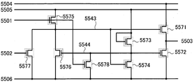
본 실시형태에서는, 반도체 장치의 일례인 표시 장치에 있어서, 동일 기판 위에 적어도 구동 회로의 일부와 화소부에 배치하는 박막 트랜지스터를 제작하는 예에 대해서 이하에 설명한다.In this embodiment, in the display device which is an example of a semiconductor device, an example of manufacturing a thin film transistor disposed on at least part of a driving circuit and a pixel portion on the same substrate will be described below.
화소부에 배치하는 박막 트랜지스터는, 실시형태 2에 따라 형성한다. 또한, 실시형태 1 내지 실시형태 3에 나타내는 박막 트랜지스터는, n채널형 TFT이기 때문에, 구동 회로 중, n채널형 TFT로 구성할 수 있는 구동 회로의 일부를 화소부의 박막 트랜지스터와 동일 기판 위에 형성한다.The thin film transistor disposed in the pixel portion is formed according to the second embodiment. In addition, since the thin film transistors shown in
반도체 장치의 일례인 액티브 매트릭스형 액정 표시 장치의 블록도의 일례를 도 15a에 도시한다. 도 15a에 도시하는 표시 장치는, 기판(5300) 위에 표시 소자를 구비한 화소를 복수 갖는 화소부(5301)와 각 화소를 선택하는 주사선 구동 회로(5302)와, 선택된 화소에의 비디오 신호의 입력을 제어하는 신호선 구동 회로(5303)를 갖는다.An example of a block diagram of an active matrix liquid crystal display device which is an example of a semiconductor device is shown in FIG. 15A. The display device shown in FIG. 15A includes a
화소부(5301)는 신호선 구동 회로(5303)로부터 열 방향으로 연장하여 배치된 복수의 신호선(S1 내지 Sm)(도시하지 않는다)에 의하여 신호선 구동 회로(5303)와 접속되고, 주사선 구동 회로(5302)로부터 행 방향으로 연장하여 배치된 복수의 주사선(G1 내지 Gn)(도시하지 않는다)에 의하여 주사선 구동 회로(5302)와 접속되고, 신호선(S1 내지 Sm) 및 주사선(G1 내지 Gn)에 대응하여 매트릭스 상태로 배치된 복수의 화소(도시하지 않는다)를 갖는다. 그리고, 각 화소는 신호선(Sj)(신호선(S1 내지 Sm) 중 어느 하나), 주사선(Gi)(주사선(G1 내지 Gn) 중 어느 하나)과 접속된다.The
또한, 실시형태 1 내지 실시형태 3에 나타내는 박막 트랜지스터는, n채널형 TFT이고, n채널형 TFT로 구성하는 신호선 구동 회로에 대하여 도 16을 사용하여 설명한다.In addition, the thin film transistors shown in
도 16에 도시하는 신호선 구동 회로는 드라이버 IC(5601), 스위치군(5602_1 내지 5602_M), 제 1 배선(5611), 제 2 배선(5612), 제 3 배선(5613) 및 배선(5621_1 내지 5621_M)을 갖는다. 스위치군(5602_1 내지 5602_M) 각각은 제 1 박막 트랜지스터(5603a), 제 2 박막 트랜지스터(5603b) 및 제 3 박막 트랜지스터(5603c)를 갖는다.The signal line driver circuit shown in FIG. 16 includes the
드라이버 IC(5601)는 제 1 배선(5611), 제 2 배선(5612), 제 3 배선(5613) 및 배선(5621_1 내지 5621_M)에 접속된다. 그리고, 스위치군(5602_1 내지 5602_M) 각각은 제 1 배선(5611), 제 2 배선(5612), 제 3 배선(5613) 및 스위치군(5602_1 내지 5602_M) 각각에 대응한 배선(5621_1 내지 5621_M)에 접속된다. 그리고, 배선(5621_1 내지 5621_M) 각각은 제 1 박막 트랜지스터(5603a), 제 2 박막 트랜지스터(5603b) 및 제 3 박막 트랜지스터(5603c)를 통하여 3개의 신호선(신호선(Sm-2), 신호선(Sm-1), 신호선(Sm)(m=3M))에 접속된다. 예를 들어, J열째의 배선(5621_J(배선(5621_1) 내지 배선(5621_M) 중 어느 하나))은 스위치군(5602_J)이 갖는 제 1 박막 트랜지스터(5603a), 제 2 박막 트랜지스터(5603b) 및 제 3 박막 트랜지스터(5603c)를 통하여 신호선(Sj-2), 신호선(Sj-1), 신호선(Sj)(j=3J)에 접속된다.The
또한, 제 1 배선(5611), 제 2 배선(5612) 및 제 3 배선(5613)에는 각각 신호가 입력된다.In addition, a signal is input to each of the
또한, 드라이버 IC(5601)는 단결정 반도체를 사용하여 형성되는 것이 바람직하다. 또한, 스위치군(5602_1 내지 5602_M)은 화소부와 동일 기판 위에 형성되는 것이 바람직하다. 따라서, 드라이버 IC(5601)와 스위치군(5602_1 내지 5602_M)은 FPC 등을 통하여 접속하면 좋다. 또는 화소부와 동일한 기판 위에 접합 등 행함으로써 단결정 반도체층을 형성하여 드라이버 IC(5601)를 형성하여도 좋다.In addition, the
다음에, 도 16에 도시한 신호선 구동 회로의 동작에 대하여, 도 17의 타이밍 차트를 참조하여 설명한다. 또한, 도 17의 타이밍 차트는 i행째의 주사선(Gi)이 선택되는 경우의 타이밍 차트를 도시한다. 또한, i행째의 주사선(Gi)의 선택 기간은 제 1 서브 선택 기간 T1, 제 2 서브 선택 기간 T2 및 제 3 서브 선택 기간 T3으로 분할된다. 또한, 도 16의 신호선 구동 회로는 다른 행의 주사선이 선택되는 경우에도 도 17과 같은 동작을 행한다.Next, the operation of the signal line driver circuit shown in FIG. 16 will be described with reference to the timing chart of FIG. 17. 17 shows a timing chart when the i-th scanning line Gi is selected. The selection period of the i-th scanning line Gi is divided into a first sub-selection period T1, a second sub-selection period T2, and a third sub-selection period T3. In addition, the signal line driver circuit of FIG. 16 performs the same operation as that of FIG. 17 even when scanning lines of other rows are selected.
또한, 도 17의 타이밍 차트는 J열째의 배선(5621_J)이 제 1 박막 트랜지스터(5603a), 제 2 박막 트랜지스터(5603b) 및 제 3 박막 트랜지스터(5603c)를 통하여 신호선(Sj-2), 신호선(Sj-1), 신호선(Sj)에 접속되는 경우에 대하여 도시한다.In addition, in the timing chart of FIG. 17, the wiring line 5221_J of the J-th column is connected to the signal line Sj-2 and the signal line through the first
또한, 도 17의 타이밍 차트는 i행째의 주사선(Gi)이 선택되는 타이밍, 제 1 박막 트랜지스터(5603a)의 온 및 오프의 타이밍(5703a), 제 2 박막 트랜지스터(5603b)의 온 및 오프의 타이밍(5703b), 제 3 박막 트랜지스터(5603c)의 온 및 오프의 타이밍(5703c) 및 J열째의 배선(5621_J)에 입력되는 신호(5721_J)를 도시한다.In addition, the timing chart of FIG. 17 includes a timing at which the i-th scan line Gi is selected, a
또한, 배선(5621_1 내지 5621_M)에는 제 1 서브 선택 기간 T1, 제 2 서브 선택 기간 T2 및 제 3 서브 선택 기간 T3에 있어서, 각각 다른 비디오 신호가 입력된다. 예를 들어, 제 1 서브 선택 기간 T1에 있어서 배선(5621_J)에 입력되는 비디오 신호는 신호선(Sj-2)에 입력되고, 제 2 서브 선택 기간 T2에 있어서 배선(5621_J)에 입력되는 비디오 신호는 신호선(Sj-1)에 입력되고, 제 3 서브 선택 기간 T3에 있어서 배선(5621_J)에 입력되는 비디오 신호는 신호선(Sj)에 입력된다. 또한, 제 1 서브 선택 기간 T1, 제 2 서브 선택 기간 T2 및 제 3 서브 선택 기간 T3에 있어서, 배선(5621_J)에 입력되는 비디오 신호를 각각 Data_j-2, Data_j-1, Data_j로 한다.Further, different video signals are input to the wirings 5221_1 to 5621_M in the first sub-selection period T1, the second sub-selection period T2, and the third sub-selection period T3, respectively. For example, the video signal input to the wiring 5221_J in the first sub-selection period T1 is input to the signal line Sj-2, and the video signal input to the wiring 5561_J in the second sub-selection period T2. The video signal input to the signal line Sj-1 and to the wiring 5221_J in the third sub-selection period T3 is input to the signal line Sj. In the first sub-selection period T1, the second sub-selection period T2, and the third sub-selection period T3, the video signals input to the wiring 5221_J are respectively Data_j-2, Data_j-1, and Data_j.
도 17에 도시하는 바와 같이, 제 1 서브 선택 기간 T1에 있어서 제 1 박막 트랜지스터(5603a)가 온 되고, 제 2 박막 트랜지스터(5603b) 및 제 3 박막 트랜지스터(5603c)가 오프 된다. 이 때, 배선(5621_J)에 입력되는 Data_j-2가, 제 1 박막 트랜지스터(5603a)를 통하여 신호선(Sj-2)에 입력된다. 제 2 서브 선택 기간 T2에서는 제 2 박막 트랜지스터(5603b)가 온 되고, 제 1 박막 트랜지스터(5603a) 및 제 3 박막 트랜지스터(5603c)가 오프 된다. 이 때, 배선(5621_J)에 입력되는 Data_j-1이, 제 2 박막 트랜지스터(5603b)를 통하여 신호선(Sj-1)에 입력된다. 제 3 서브 선택 기간 T3에서는 제 3 박막 트랜지스터(5603c)가 온 되고, 제 1 박막 트랜지스터(5603a) 및 제 2 박막 트랜지스터(5603b)가 오프 된다. 이 때, 배선(5621_J)에 입력되는 Data_j가, 제 3 박막 트랜지스터(5603c)를 통하여 신호선(Sj)에 입력된다.As shown in FIG. 17, in the first sub-selection period T1, the first
이상으로부터, 도 16의 신호선 구동 회로는 1게이트 선택 기간을 3개로 분할함으로써, 1게이트 선택 기간 중에 1개의 배선(5621)으로부터 3개의 신호선에 비디오 신호를 입력할 수 있다. 따라서, 도 16의 신호선 구동 회로는 드라이버 IC(5601)가 형성되는 기판과 화소부가 형성되는 기판과의 접속 개수를 신호선의 개수와 비교하여 약 1/3로 할 수 있다. 접속 개수가 약 1/3이 됨으로써, 도 16의 신호선 구동 회로는 신뢰성, 수율 등을 향상시킬 수 있다.As described above, the signal line driver circuit of FIG. 16 divides one gate selection period into three, so that a video signal can be input to three signal lines from one wiring 5561 during one gate selection period. Therefore, in the signal line driver circuit of FIG. 16, the number of connections between the substrate on which the
또한, 도 17에 도시하는 바와 같이, 1게이트 선택 기간을 복수의 서브 선택 기간으로 분할하여, 복수의 서브 선택 기간 각각에 있어서 어느 1개의 배선으로부터 복수의 신호선 각각에 비디오 신호를 입력할 수 있으면, 박막 트랜지스터의 배치나 개수, 구동 방법 등은 한정되지 않는다.As shown in Fig. 17, if one gate selection period is divided into a plurality of sub selection periods, and a video signal can be input to each of the plurality of signal lines from any one wiring in each of the plurality of sub selection periods, The arrangement, number, driving method, etc. of the thin film transistors are not limited.
예를 들어, 3개 이상의 서브 선택 기간 각각에 있어서 1개의 배선으로부터 3개 이상의 신호선 각각에 비디오 신호를 입력하는 경우는 박막 트랜지스터 및 박막 트랜지스터를 제어하기 위한 배선을 추가하면 좋다. 다만, 1게이트 선택 기간을 4개 이상의 서브 선택 기간으로 분할하면, 1개의 서브 선택 기간이 짧아진다. 따라서, 1게이트 선택 기간은 2개 또는 3개의 서브 선택 기간으로 분할되는 것이 바람직하다.For example, when a video signal is input to each of three or more signal lines from one wiring in each of the three or more sub-selection periods, a thin film transistor and a wiring for controlling the thin film transistor may be added. However, if one gate selection period is divided into four or more sub selection periods, one sub selection period is shortened. Therefore, one gate selection period is preferably divided into two or three sub selection periods.
다른 예로서, 도 18의 타이밍 차트에 도시하는 바와 같이, 1개의 선택 기간을 프리차지 기간 Tp, 제 1 서브 선택 기간 T1, 제 2 서브 선택 기간 T2, 제 3 서브 선택 기간 T3으로 분할하여도 좋다. 또한, 도 18의 타이밍 차트는 i행째의 주사선 (Gi)가 선택되는 타이밍, 제 1 박막 트랜지스터(5603a)의 온 및 오프의 타이밍(5803a), 제 2 박막 트랜지스터(5603b)의 온 및 오프의 타이밍(5803b), 제 3 박막 트랜지스터(5603c)의 온 및 오프의 타이밍(5803c) 및 J열째의 배선(5621_J)에 입력되는 신호(5821_J)를 도시한다. 도 18에 도시하는 바와 같이, 프리차지 기간 Tp에 있어서 제 1 박막 트랜지스터(5603a), 제 2 박막 트랜지스터(5603b), 및 제 3 박막 트랜지스터(5603c)가 온 된다. 이 때, 배선(5621_J)에 입력되는 프리차지 전압 Vp가 제 1 박막 트랜지스터(5603a), 제 2 박막 트랜지스터(5603b) 및 제 3 박막 트랜지스터(5603c)를 통하여, 각각 신호선(Sj-2), 신호선(Sj-1), 신호선(Sj)에 입력된다. 제 1 서브 선택 기간 T1에 있어서 제 1 박막 트랜지스터(5603a)가 온 되고, 제 2 박막 트랜지스터(5603b), 및 제 3 박막 트랜지스터(5603c)가 오프 된다. 이 때, 배선(5621_J)에 입력되는 Data_j-2가, 제 1 박막 트랜지스터(5603a)를 통하여 신호선(Sj-2)에 입력된다. 제 2 서브 선택 기간 T2에서는 제 2 박막 트랜지스터(5603b)가 온 되고, 제 1 박막 트랜지스터(5603a) 및 제 3 박막 트랜지스터(5603c)가 오프 된다. 이 때, 배선(5621_J)에 입력되는 Data_j-1이, 제 2 박막 트랜지스터(5603b)를 통하여 신호선(Sj-1)에 입력된다. 제 3 서브 선택 기간 T3에서는 제 3 박막 트랜지스터(5603c)가 온 되고, 제 1 박막 트랜지스터(5603a) 및 제 2 박막 트랜지스터(5603b)가 오프 된다. 이 때, 배선(5621_J)에 입력되는 Data_j가, 제 3 박막 트랜지스터(5603c)를 통하여 신호선(Sj)에 입력된다.As another example, as shown in the timing chart of FIG. 18, one selection period may be divided into a precharge period Tp, a first subselection period T1, a second subselection period T2, and a third subselection period T3. . In addition, the timing chart of FIG. 18 shows the timing at which the i-th scan line Gi is selected, the timing 5580a for turning on and off the first
이상으로부터, 도 18의 타이밍 차트를 적용한 도 16의 신호선 구동 회로는 서브 선택 기간 전에 프리차지 선택 기간을 형성함으로써, 신호선을 프리차지할 수 있기 때문에, 화소에 대한 비디오 신호의 기록을 고속으로 행할 수 있다. 또한, 도 18에 있어서, 도 17와 마찬가지인 것에 관해서는 공통되는 부호를 사용하여 도시하고, 동일한 부분 또는 같은 기능을 갖는 부분의 상세한 설명은 생략한다.From the above, the signal line driver circuit of FIG. 16 to which the timing chart of FIG. 18 is applied can precharge the signal lines by forming the precharge selection period before the sub selection period, and therefore, the video signal recording to the pixel can be performed at high speed. . In addition, in FIG. 18, the thing similar to FIG. 17 is shown using the code | symbol common, and detailed description of the same part or the part which has the same function is abbreviate | omitted.
또한, 주사선 구동 회로의 구성에 대하여 설명한다. 주사선 구동 회로는, 시프트 레지스터, 버퍼를 갖는다. 또한, 경우에 따라서는 레벨 시프터를 가져도 좋다. 주사선 구동 회로에 있어서, 시프트 레지스터에 클록 신호(CLK) 및 스타트 펄스 신호(SP)가 입력됨으로써, 선택 신호가 생성된다. 생성된 선택 신호는 버퍼에 있어서 완충 증폭되고, 대응하는 주사선에 공급된다. 주사선에는 1라인분의 화소의 트랜지스터의 게이트 전극이 접속된다. 그리고, 1라인분의 화소의 트랜지스터를 일제히 온해야 하기 때문에, 버퍼는 큰 전류를 흘릴 수 있는 것이 사용된다.In addition, the configuration of the scan line driver circuit will be described. The scan line driver circuit has a shift register and a buffer. In some cases, a level shifter may be provided. In the scan line driver circuit, the clock signal CLK and the start pulse signal SP are input to the shift register, whereby a selection signal is generated. The generated selection signal is buffered and amplified in the buffer and supplied to the corresponding scan line. Gate electrodes of transistors of pixels for one line are connected to the scan line. Since the transistors of one line of pixels must all be turned on at the same time, a buffer capable of flowing a large current is used.
주사선 구동 회로의 일부에 사용하는 시프트 레지스터의 일 형태에 대하여 도 19 및 도 20를 사용하여 설명한다.One form of the shift register used for a part of the scanning line driver circuit will be described with reference to FIGS. 19 and 20.
도 19에 시프트 레지스터의 회로 구성을 도시한다. 도 19에 도시하는 시프트 레지스터는 복수의 플립플롭(5701_1) 내지 플립플롭(5701_n)으로 구성된다. 또한, 제 1 클록 신호, 제 2 클록 신호, 스타트 펄스 신호, 리셋 신호가 입력되어 동작한다.19 shows the circuit configuration of the shift register. The shift register shown in FIG. 19 is composed of a plurality of flip-flops 5701_1 to flip-flops 5701_n. Also, the first clock signal, the second clock signal, the start pulse signal, and the reset signal are input to operate.
도 19의 시프트 레지스터의 접속 관계에 대하여 설명한다. 1단째의 플립플롭(5701_1)은, 제 1 배선(5711), 제 2 배선(5712), 제 4 배선(5714), 제 5 배선(5715), 제 7 배선(5717_1), 및 제 7 배선(5717_2)과 접속된다. 또한, 2단째의 플립플롭(5701_2)은, 제 3 배선(5713), 제 4 배선(5714), 제 5 배선(5715), 제 7 배선(5717_1), 제 7 배선(5717_2), 및 제 7 배선(5717_3)과 접속된다.The connection relationship of the shift register of FIG. 19 is demonstrated. The first stage flip-flop 5701_1 includes a
마찬가지로, i단째의 플립플롭(5701_i)(플립플롭(5701_1) 내지 (5701_n) 중 어느 하나)은, 제 2 배선(5712) 또는 제 3 배선(5713) 중의 한쪽, 제 4 배선(5714), 제 5 배선(5715), 제 7 배선(5717_i-1), 제 7 배선(5717_i), 및 제 7 배선(5717_i+1)과 접속된다. 여기서, i가 홀수인 경우에는, i단째의 플립플롭(5701_i)은 제 2 배선(5712)과 접속되고, i가 짝수인 경우에는, i단째의 플립플롭(5701_i)은 제 3 배선(5713)과 접속된다.Similarly, the i-stage flip-flop 5701_i (any one of the flip-flops 5701_1 to 5701_n) is either one of the
또한, n단째의 플립플롭(5701_n)은, 제 2 배선(5712) 또는 제 3 배선(5713) 중의 한쪽, 제 4 배선(5714), 제 5 배선(5715), 제 7 배선(5717_n-1), 제 7 배선(5717_n), 및 제 6 배선(5716)과 접속된다.The n-th flip-flop 5701_n includes one of the
또한, 제 1 배선(5711), 제 2 배선(5712), 제 3 배선(5713), 제 6 배선(5716)을 각각 제 1 신호선, 제 2 신호선, 제 3 신호선, 제 4 신호선이라고 불러도 좋다. 또한, 제 4 배선(5714), 제 5 배선(5715)을 각각 제 1 전원선, 제 2 전원선이라고 불러도 좋다.The
다음에, 도 19에 도시하는 플립플롭의 자세한 내용에 대하여, 도 20를 사용하여 설명한다. 도 20에 도시하는 플립플롭은 제 1 박막 트랜지스터(5571), 제 2 박막 트랜지스터(5572), 제 3 박막 트랜지스터(5573), 제 4 박막 트랜지스터(5574), 제 5 박막 트랜지스터(5575), 제 6 박막 트랜지스터(5576), 제 7 박막 트랜지스터(5577) 및 제 8 박막 트랜지스터(5578)를 갖는다. 또한, 제 1 박막 트랜지스터(5571), 제 2 박막 트랜지스터(5572), 제 3 박막 트랜지스터(5573), 제 4 박막 트랜지스터(5574), 제 5 박막 트랜지스터(5575), 제 6 박막 트랜지스터(5576), 제 7 박막 트랜지스터(5577) 및 제 8 박막 트랜지스터(5578)는 n채널형 트랜지스터이며, 게이트-소스간 전압(Vgs)이 임계값 전압(Vth)을 초과할 때, 도통 상태가 되는 것으로 한다.Next, details of the flip flop shown in FIG. 19 will be described with reference to FIG. 20. The flip-flop illustrated in FIG. 20 includes the first
또한, 도 20에 도시하는 플립플롭은 제 1 배선(5501), 제 2 배선(5502), 제 3 배선(5503), 제 4 배선(5504), 제 5 배선(5505), 및 제 6 배선(5506)을 갖는다.In addition, the flip-flop shown in FIG. 20 includes the
여기서는, 모든 박막 트랜지스터는 인핸스먼트형의 n채널형 트랜지스터로 하는 예를 나타내지만, 특히 한정되지 않고, 예를 들어, 디플리션형의 n채널형 트랜지스터를 사용해도 구동 회로를 구동시킬 수 있다.Here, although all the thin film transistors show an example of an enhancement type n-channel transistor, the present invention is not particularly limited. For example, even when a depletion n-channel transistor is used, the driving circuit can be driven.
다음에, 도 20에 도시하는 플립플롭의 접속 구성에 대해서 이하에 나타낸다.Next, the connection structure of the flip-flop shown in FIG. 20 is shown below.
제 1 박막 트랜지스터(5571)의 제 1 전극(소스 전극 또는 드레인 전극의 한쪽)이 제 4 배선(5504)에 접속되고, 제 1 박막 트랜지스터(5571)의 제 2 전극(소스 전극 또는 드레인 전극의 다른 쪽)이 제 3 배선(5503)에 접속된다.The first electrode (one of the source electrode or the drain electrode) of the first
제 2 박막 트랜지스터(5572)의 제 1 전극이 제 6 배선(5506)에 접속되고, 제 2 박막 트랜지스터(5572)의 제 2 전극이 제 3 배선(5503)에 접속된다.The first electrode of the second
제 3 박막 트랜지스터(5573)의 제 1 전극이 제 5 배선(5505)에 접속되고, 제 3 박막 트랜지스터(5573)의 제 2 전극이 제 2 박막 트랜지스터(5572)의 게이트 전극에 접속되고, 제 3 박막 트랜지스터(5573)의 게이트 전극이 제 5 배선(5505)에 접속된다.A first electrode of the third
제 4 박막 트랜지스터(5574)의 제 1 전극이 제 6 배선(5506)에 접속되고, 제 4 박막 트랜지스터(5574)의 제 2 전극이 제 2 박막 트랜지스터(5572)의 게이트 전극에 접속되고, 제 4 박막 트랜지스터(5574)의 게이트 전극이 제 1 박막 트랜지스터(5571)의 게이트 전극에 접속된다.A first electrode of the fourth
제 5 박막 트랜지스터(5575)의 제 1 전극이 제 5 배선(5505)에 접속되고, 제 5 박막 트랜지스터(5575)의 제 2 전극이 제 1 박막 트랜지스터(5571)의 게이트 전극에 접속되고, 제 5 박막 트랜지스터(5575)의 게이트 전극이 제 1 배선(5501)에 접속된다.The first electrode of the fifth
제 6 박막 트랜지스터(5576)의 제 1 전극이 제 6 배선(5506)에 접속되고, 제 6 박막 트랜지스터(5576)의 제 2 전극이 제 1 박막 트랜지스터(5571)의 게이트 전극에 접속되고, 제 6 박막 트랜지스터(5576)의 게이트 전극이 제 2 박막 트랜지스터(5572)의 게이트 전극에 접속된다.The first electrode of the sixth
제 7 박막 트랜지스터(5577)의 제 1 전극이 제 6 배선(5506)에 접속되고, 제 7 박막 트랜지스터(5577)의 제 2 전극이 제 1 박막 트랜지스터(5571)의 게이트 전극에 접속되고, 제 7 박막 트랜지스터(5577)의 게이트 전극이 제 2 배선(5502)에 접속된다.The first electrode of the seventh
제 8 박막 트랜지스터(5578)의 제 1 전극이 제 6 배선(5506)에 접속되고, 제 8 박막 트랜지스터(5578)의 제 2 전극이 제 2 박막 트랜지스터(5572)의 게이트 전극에 접속되고, 제 8 박막 트랜지스터(5578)의 게이트 전극이 제 1 배선(5501)에 접속된다.The first electrode of the eighth
또한, 제 1 박막 트랜지스터(5571)의 게이트 전극, 제 4 박막 트랜지스터(5574)의 게이트 전극, 제 5 박막 트랜지스터(5575)의 제 2 전극, 제 6 박막 트랜지스터(5576)의 제 2 전극 및 제 7 박막 트랜지스터(5577)의 제 2 전극의 접속 개소를 노드(5543)로 한다. 또한, 제 2 박막 트랜지스터(5572)의 게이트 전극, 제 3 박막 트랜지스터(5573)의 제 2 전극, 제 4 박막 트랜지스터(5574)의 제 2 전극, 제 6 박막 트랜지스터(5576)의 게이트 전극 및 제 8 박막 트랜지스터(5578)의 제 2 전극의 접속 개소를 노드(5544)로 한다.The gate electrode of the first
또한, 제 1 배선(5501), 제 2 배선(5502), 제 3 배선(5503) 및 제 4 배선(5504)을, 각각 제 1 신호선, 제 2 신호선, 제 3 신호선 및 제 4 신호선이라고 불러도 좋다. 또한, 제 5 배선(5505)을 제 1 전원선, 제 6 배선(5506)을 제 2 전원선이라고 불러도 좋다.The
i단째의 플립플롭(5701_i)에 있어서, 도 20 중의 제 1 배선(5501)과 도 19 중의 제 7 배선(5717_i-1)이 접속된다. 또한, 도 20 중의 제 2 배선(5502)과 도 19 중의 제 7 배선(5717_i+1)이 접속된다. 또한, 도 20 중의 제 3 배선(5503)과 제 7 배선(5717_i)이 접속된다. 또한, 도 20 중의 제 6 배선(5506)과 제 5 배선(5715)이 접속된다.In the i-th flip-flop 5701_i, the
i가 홀수인 경우, 도 20 중의 제 4 배선(5504)은 도 19 중의 제 2 배선(5712)과 접속되고, i가 짝수인 경우에는, 도 19 중의 제 3 배선(5713)과 접속된다. 또한, 도 20 중의 제 5 배선(5505)과 도 19 중의 제 4 배선(5714)이 접속된다.When i is odd, the
다만, 1단째의 플립플롭(5701_1)에 있어서, 도 20 중의 제 1 배선(5501)은 도 19 중의 제 1 배선(5711)에 접속된다. 또한, n단째의 플립플롭(5701_n)에 있어서, 도 20 중의 제 2 배선(5502)은 도 19 중의 제 6 배선(5716)에 접속된다.In the flip-flop 5801_1 of the first stage, however, the
또한, 신호선 구동 회로 및 주사선 구동 회로를 실시형태 1 내지 실시형태 3에 나타내는 n채널형 TFT만으로 제작할 수도 있다. 실시형태 1 내지 실시형태 3에 나타내는 n채널형 TFT는 트랜지스터의 이동도가 크기 때문에, 구동 회로의 구동 주파수를 높게 할 수 있다. 또한, 실시형태 1 내지 실시형태 3에 나타내는 n채널형 TFT는 In-Ga-Zn-O계 비단결정막으로 대표되는 산화물 반도체층을 사용함으로써, 기생 용량이 저감되기 때문에, 주파수 특성(f 특성이라고 불린다)이 높다. 예를 들어, 실시형태 1 내지 실시형태 3에 나타내는 n채널형 TFT를 사용한 주사선 구동 회로는 고속으로 동작시킬 수 있기 때문에, 프레임 주파수를 높게 하는 것, 또는 흑색 화면 삽입 등도 실현할 수 있다.In addition, the signal line driver circuit and the scan line driver circuit can also be manufactured using only the n-channel TFTs shown in the first to third embodiments. Since the n-channel TFTs shown in
또한, 주사선 구동 회로의 트랜지스터의 채널 폭을 크게 하는 것이나, 복수의 주사선 구동 회로를 배치하는 것 등에 의하여, 더욱 높은 프레임 주파수를 실현할 수 있다. 복수의 주사선 구동 회로를 배치하는 경우는, 짝수행의 주사선을 구동하기 위한 주사선 구동 회로를 한쪽에 배치하고, 홀수행의 주사선을 구동하기 위한 주사선 구동 회로를 그 반대 측에 배치함으로써, 프레임 주파수를 높게 하는 것을 실현할 수 있다. 또한, 복수의 주사선 구동 회로에 의하여 같은 주사선에 신호를 출력하면, 표시 장치의 대형화에 유리하다.Further, higher frame frequencies can be realized by increasing the channel width of the transistor of the scan line driver circuit, by arranging a plurality of scan line driver circuits. In the case of arranging a plurality of scan line driver circuits, the frame frequency can be adjusted by arranging a scan line driver circuit for driving even-numbered scan lines on one side and a scan line driver circuit for driving odd-numbered scan lines on the other side. It can realize to make high. In addition, outputting signals to the same scan line by a plurality of scan line driver circuits is advantageous in increasing the size of the display device.
또한, 반도체 장치의 일례인 액티브 매트릭스형 발광 표시 장치를 제작하는 경우, 적어도 하나의 화소에 복수의 박막 트랜지스터를 배치하기 때문에, 주사선 구동 회로를 복수 배치하는 것이 바람직하다. 액티브 매트릭스형 발광 표시 장치의 블록도의 일례를 도 15b에 도시한다.In the case of manufacturing an active matrix type light emitting display device which is an example of a semiconductor device, since a plurality of thin film transistors are arranged in at least one pixel, it is preferable to arrange a plurality of scan line driver circuits. An example of a block diagram of an active matrix light emitting display is shown in FIG. 15B.
도 15b에 도시하는 발광 표시 장치는, 기판(5400) 위에 표시 소자를 구비한 화소를 복수 갖는 화소부(5401)와, 각 화소를 선택하는 제 1 주사선 구동 회로(5402), 및 제 2 주사선 구동 회로(5404)와, 선택된 화소에의 비디오 신호의 입력을 제어하는 신호선 구동 회로(5403)를 갖는다.The light emitting display shown in FIG. 15B includes a
도 15b에 도시하는 발광 표시 장치의 화소에 입력되는 비디오 신호를 디지털 형식으로 하는 경우, 화소는 트랜지스터의 온 및 오프의 전환에 따라, 발광 또는 비발광의 상태가 된다. 따라서, 면적 계조법 또는 시간 계조법을 사용하여 계조의 표시를 행할 수 있다. 면적 계조법은 1화소를 복수의 부화소로 분할하고, 각 부화소를 독립적으로 비디오 신호에 의거하여 구동시킴으로써 계조 표시를 행하는 구동법이다. 또한, 시간 계조법은 화소가 발광하는 기간을 제어함으로써, 계조 표시를 행하는 구동법이다.When the video signal input to the pixel of the light emitting display device shown in Fig. 15B is a digital format, the pixel is in the state of light emission or non-emission according to the switching of the transistor on and off. Therefore, the gray scale can be displayed using the area gray scale method or the time gray scale method. The area gradation method is a driving method in which gradation display is performed by dividing one pixel into a plurality of subpixels and driving each subpixel independently based on a video signal. The time gradation method is a driving method for performing gradation display by controlling the period during which the pixels emit light.
발광 소자는, 액정 소자 등과 비교하여 응답 속도가 빠르기 때문에, 액정 소자보다 시간 계조법에 적합하다. 구체적으로는, 시간 계조법으로 표시를 행하는 경우, 1프레임 기간을 복수의 서브 프레임 기간으로 분할한다. 그리고, 비디오 신호에 따라, 각 서브 프레임 기간에 있어서, 화소의 발광 소자를 발광 또는 비발광의 상태로 한다. 복수의 서브 프레임 기간으로 분할함으로써, 1프레임 기간 중에 화소가 실제로 발광하는 기간의 총합 길이를 비디오 신호에 의하여 제어할 수 있고, 계조를 표시할 수 있다.Since a light emitting element has a quick response speed compared with a liquid crystal element etc., it is more suitable for the time gradation method than a liquid crystal element. Specifically, when displaying by the time gray scale method, one frame period is divided into a plurality of sub frame periods. Then, in accordance with the video signal, the light emitting element of the pixel is in the state of light emission or non-light emission in each sub frame period. By dividing into a plurality of sub frame periods, the total length of the periods during which the pixels actually emit light in one frame period can be controlled by the video signal, and gray levels can be displayed.
또한, 도 15b에 도시하는 발광 표시 장치에서는, 하나의 화소에 2개의 스위칭용 TFT를 배치하는 경우, 한쪽의 스위칭용 TFT의 게이트 배선인 제 1 주사선에 입력되는 신호를 제 1 주사선 구동 회로(5402)에서 생성하고, 다른 쪽의 스위칭용 TFT의 게이트 배선인 제 2 주사선에 입력되는 신호를 제 2 주사선 구동 회로(5404)에서 생성하는 예를 나타내지만, 제 1 주사선에 입력되는 신호와, 제 2 주사선에 입력되는 신호의 양쪽 모두를 하나의 주사선 구동 회로에서 생성하도록 하여도 좋다. 또한, 예를 들어, 1개의 화소가 갖는 스위칭용 TFT의 개수에 따라, 스위칭 소자의 동작을 제어하는 데에 사용되는 주사선이 각 화소에 복수 형성될 수도 있다. 이 경우, 복수의 주사선에 입력되는 신호를 모두 다 하나의 주사선 구동 회로에서 생성하여도 좋고, 복수의 각 주사선 구동 회로에서 생성하여도 좋다.In the light emitting display device shown in Fig. 15B, when two switching TFTs are arranged in one pixel, the first scan
또한, 발광 표시 장치에 있어서도, 구동 회로 중, n채널형 TFT로 구성할 수 있는 구동 회로의 일부를 화소부의 박막 트랜지스터와 동일 기판 위에 형성할 수 있다. 또한, 신호선 구동 회로 및 주사선 구동 회로를 실시형태 1 내지 실시형태 3에 나타내는 n채널형 TFT만으로 제작할 수도 있다.Also in the light emitting display device, a part of the driver circuit which can be constituted by the n-channel TFT among the driver circuits can be formed on the same substrate as the thin film transistor of the pixel portion. In addition, the signal line driver circuit and the scan line driver circuit can also be manufactured using only the n-channel TFTs shown in the first to third embodiments.
이상의 공정으로 반도체 장치로서 전기 특성이 안정된 신뢰성이 높은 표시 장치를 제작할 수 있다.In the above process, a highly reliable display device having stable electrical characteristics as a semiconductor device can be manufactured.
또한, 본 실시형태에 나타내는 구성은, 다른 실시형태에 기재한 구성을 적절히 조합하여 사용할 수 있다.In addition, the structure shown in this embodiment can be used combining suitably the structure described in other embodiment.
(실시형태 5)(Embodiment 5)
실시형태 1 내지 실시형태 3에 나타내는 박막 트랜지스터를 제작하고, 상기 박막 트랜지스터를 화소부, 또한 구동 회로에 사용하여 표시 기능을 갖는 반도체 장치(표시 장치라고도 한다)를 제작할 수 있다. 또한, 실시형태 1 내지 실시형태 3에 나타내는 박막 트랜지스터를 사용한 구동 회로의 일부 또는 전체를 화소부와 같은 기판 위에 일체 형성하여 시스템 온 패널을 형성할 수 있다.The thin film transistors shown in
표시 장치는 표시 소자를 포함한다. 표시 소자로서는 액정 소자(액정 표시 소자라고도 한다), 발광 소자(발광 표시 소자라고도 한다)를 사용할 수 있다. 발광 소자는 전류 또는 전압에 의하여 휘도가 제어되는 소자를 그 범주에 포함하고, 구체적으로는 무기 EL(Electro Luminescence), 유기 EL 등이 포함된다. 또한, 전자 잉크 등, 전기적 작용에 의하여 콘트라스트가 변화하는 표시 매체도 적용할 수 있다.The display device includes a display element. As the display element, a liquid crystal element (also called a liquid crystal display element) and a light emitting element (also called a light emitting display element) can be used. The light emitting device includes, in its category, an element whose luminance is controlled by a current or a voltage, and specifically includes an inorganic EL (Electro Luminescence), an organic EL, and the like. In addition, a display medium whose contrast is changed by an electrical action such as an electronic ink can also be applied.
또한, 표시 장치는, 표시 소자가 밀봉된 상태의 패널과, 상기 패널에 컨트롤러를 포함하는 IC 등을 실장한 상태의 모듈을 포함한다. 또한, 상기 표시 장치를 제작하는 과정에 있어서의, 표시 소자가 완성되기 전의 일 형태에 상당하는 소자 기판에 관하여, 상기 소자 기판은 전류를 표시 소자에 공급하기 위한 수단을 복수의 각 화소에 구비한다. 소자 기판은, 구체적으로는 표시 소자의 화소 전극만이 형성된 상태라도 좋고, 화소 전극이 되는 도전막을 형성한 후이고, 에칭하여 화소 전극을 형성하기 전의 상태라도 좋고, 다양한 형태가 적합하다.The display device also includes a panel in a state where the display element is sealed, and a module in a state in which an IC including a controller is mounted on the panel. Moreover, in the element substrate which corresponds to one form before the display element is completed in the process of manufacturing the said display apparatus, the said element substrate is equipped with the means for supplying an electric current to a display element in each pixel. . Specifically, the element substrate may be in a state in which only a pixel electrode of the display element is formed, or may be formed after forming a conductive film to be a pixel electrode, and before etching to form a pixel electrode, and various forms are suitable.
또한, 본 명세서 중에서의 표시 장치는 화상 표시 디바이스, 표시 디바이스, 또는 광원(조명 장치도 포함한다)을 가리킨다. 또한, 커넥터, 예를 들어, FPC(Flexible Printed Circuit) 또는 TAB(Tape Automated Bonding) 테이프 또는 TCP(Tape Carrier Package)가 장착된 모듈, TAB 테이프나 TCP의 선단에 프린트 배선판이 설치된 모듈, 또는 표시 소자에 COG(Chip On Glass) 방식에 의하여 IC(집적 회로)가 직접 실장된 모듈도 모두 표시 장치에 포함한다.In addition, the display apparatus in this specification points out an image display device, a display device, or a light source (it also includes an illumination device). Also, a module equipped with a connector, for example, a flexible printed circuit (FPC) or tape automated bonding (TAB) tape or a tape carrier package (TCP), a module having a printed wiring board installed at the tip of the TAB tape or TCP, or a display element In the display device, all modules in which an IC (Integrated Circuit) is directly mounted by a chip on glass (COG) method are included.
본 실시형태에서는, 반도체 장치의 일 형태에 상당하는 액정 표시 패널의 외관 및 단면에 대해서, 도 21a, 도 21b, 및 도 21c를 사용하여 설명한다. 도 21a 및 도 21b는 제 1 기판(4001) 위에 형성된 실시형태 1 내지 실시형태 3에서 나타낸 In-Ga-Zn-O계 비단결정막을 대표로 하는 산화물 반도체층을 사용하는, 전기 특성이 안정된 신뢰성이 높은 박막 트랜지스터(4010, 4011), 및 액정 소자(4013)를 제 2 기판(4006)과의 사이에 씰재(4005)에 의하여 밀봉한, 패널의 평면도이며, 도 21c는 도 21a, 도 21b의 M-N에 있어서의 단면도에 상당한다.In this embodiment, the external appearance and cross section of a liquid crystal display panel corresponding to one embodiment of a semiconductor device will be described with reference to FIGS. 21A, 21B, and 21C. 21A and 21B show stable reliability of electrical characteristics using the oxide semiconductor layer represented by the In—Ga—Zn—O based non-single crystal film shown in
제 1 기판(4001) 위에 형성된 화소부(4002)와, 주사선 구동 회로(4004)를 둘러싸도록, 씰재(4005)가 형성된다. 또한 화소부(4002)와, 주사선 구동 회로(4004) 위에 제 2 기판(4006)이 형성된다. 따라서, 화소부(4002)와, 주사선 구동 회로(4004)는, 제 1 기판(4001)과 씰재(4005)와 제 2 기판(4006)에 의하여, 액정층(4008)과 함께 밀봉된다. 또한, 제 1 기판(4001) 위의 씰재(4005)에 의하여 둘러싸인 영역과는 상이한 영역에, 별도 준비된 기판 위에 단결정 반도체막 또는 다결정 반도체막으로 형성된 신호선 구동 회로(4003)가 실장된다.The
또한, 별도 형성한 구동 회로의 접속 방법은 특히 한정되는 것이 아니고, COG 방법, 와이어 본딩 방법, 또는 TAB 방법 등을 사용할 수 있다. 도 21a는 COG 방법에 의하여 신호선 구동 회로(4003)를 실장하는 예이며, 도 21b는 TAB 방법에 의하여 신호선 구동 회로(4003)를 실장하는 예이다.In addition, the connection method of the drive circuit formed separately is not specifically limited, A COG method, a wire bonding method, a TAB method, etc. can be used. 21A shows an example of mounting the signal
또한, 제 1 기판(4001) 위에 형성된 화소부(4002)와 주사선 구동 회로(4004)는 박막 트랜지스터를 복수 갖고, 도 21b에서는 화소부(4002)에 포함되는 박막 트랜지스터(4010)와 주사선 구동 회로(4004)에 포함되는 박막 트랜지스터(4011)를 예시한다. 박막 트랜지스터(4010, 4011) 위에는 절연층(4020, 4021)이 형성되어 있다.In addition, the
박막 트랜지스터(4010, 4011)는, 실시형태 1 내지 실시형태 3에 나타내는 In-Ga-Zn-O계 비단결정막을 대표로 하는 산화물 반도체층을 사용하는, 전기 특성이 안정된 신뢰성이 높은 박막 트랜지스터를 적용할 수 있다. 본 실시형태에 있어서, 박막 트랜지스터(4010, 4011)는 n채널형 박막 트랜지스터이다.As the
또한, 액정 소자(4013)가 갖는 화소 전극층(4030)은 박막 트랜지스터(4010)와 전기적으로 접속된다. 그리고 액정 소자(4013)의 대향 전극층(4031)은 제 2 기판(4006) 위에 형성된다. 화소 전극층(4030)과 대향 전극층(4031)과 액정층(4008)이 중첩하는 부분이 액정 소자(4013)에 상당한다. 또한, 화소 전극층(4030), 대향 전극층(4031)은 각각 배향막으로서 기능하는 절연층(4032, 4033)이 형성되고, 절연층(4032, 4033)을 개재하여 액정층(4008)을 협지한다.The
또한, 제 1 기판(4001), 제 2 기판(4006)으로서는, 유리, 금속(대표적으로는 스테인리스), 세라믹스, 플라스틱을 사용할 수 있다. 플라스틱으로서는 FRP(Fiberglass-Reinforced Plastics)판, PVF(폴리비닐 플로라이드) 필름, 폴리에스테르 필름, 또는 아크릴 수지 필름을 사용할 수 있다. 또한, 알루미늄 포일을 PVF 필름이나 폴리에스테르 필름으로 끼운 구조의 시트를 사용할 수도 있다.As the
또한, (4035)는 절연막을 선택적으로 에칭함으로써 얻어지는 주 형상의 스페이서이며, 화소 전극층(4030)과 대향 전극층(4031)의 사이의 거리(셀 갭)를 제어하기 위하여 형성된다. 또한, 구 형상의 스페이서를 사용하여도 좋다. 또한, 대향 전극층(4031)은 박막 트랜지스터(4010)와 동일 기판 위에 형성되는 공통 전위선과 전기적으로 접속된다. 공통 접속부를 사용하여, 한 쌍의 기판간에 배치되는 도전성 입자를 통해서 대향 전극층(4031)과 공통 전위선을 전기적으로 접속할 수 있다. 또한, 도전성 입자는 씰재(4005)에 함유시킨다.4035 is a main spacer obtained by selectively etching the insulating film, and is formed to control the distance (cell gap) between the
또한, 배향막을 사용하지 않는 블루상(blue phase)을 나타내는 액정을 사용하여도 좋다. 블루상은 액정상의 하나이며, 콜레스테릭(cholesteric) 액정을 승온하면, 콜레스테릭상으로부터 등방상으로 전이하기 직전에 발현하는 상이다. 블루상은 좁은 온도 범위에서만 발현되기 때문에, 온도 범위를 개선하기 위해서 5wt% 이상의 키랄제를 혼합시킨 액정 조성물을 사용하여 액정층(4008)에 사용한다. 블루상을 나타내는 액정과 키랄제를 포함하는 액정 조성물은 응답 속도가 10μs 내지 100μs이며 짧고, 광학적 등방성이기 때문에 배향 처리가 불필요하고, 시야각 의존성이 작다.Moreover, you may use the liquid crystal which shows the blue phase which does not use an alignment film. The blue phase is one of the liquid crystal phases, and when the cholesteric liquid crystal is heated, the blue phase is a phase which is expressed immediately before transition from the cholesteric phase to the isotropic phase. Since a blue phase is expressed only in a narrow temperature range, in order to improve a temperature range, it uses for the
또한, 본 실시형태는, 투과형 액정 표시 장치의 예이지만, 반사형 액정 표시 장치라도 적용할 수 있고, 반투과형 액정 표시 장치라도 적용할 수 있다.In addition, although this embodiment is an example of a transmissive liquid crystal display device, even a reflective liquid crystal display device is applicable and even a transflective liquid crystal display device is applicable.
또한, 본 실시형태의 액정 표시 장치에서는, 기판의 외측(시인 측)에 편광판을 형성하고, 내측에 착색층, 표시 소자에 사용하는 전극층의 순서로 형성하는 예를 나타내지만, 편광판은 기판의 내측에 형성하여도 좋다. 또한, 편광판과 착색층의 적층 구조도 본 실시형태에 한정되지 않고, 편광판 및 착색층의 재료나 제작 공정 조건에 따라 적절하게 설정하면 좋다. 또한, 블랙 매트릭스로서 기능하는 차광막을 형성하여도 좋다.In addition, in the liquid crystal display of this embodiment, although the polarizing plate is formed in the outer side (viewing side) of a board | substrate, the example which forms in order of the colored layer and the electrode layer used for a display element is shown inside, but a polarizing plate is the inside of a board | substrate. It may be formed on. In addition, the laminated structure of a polarizing plate and a colored layer is not limited to this embodiment, What is necessary is just to set suitably according to the material and manufacturing process conditions of a polarizing plate and a colored layer. Moreover, you may form the light shielding film which functions as a black matrix.
또한, 본 실시형태에서는, 박막 트랜지스터의 표면 요철을 저감하기 위하여, 및 박막 트랜지스터의 신뢰성을 향상시키기 위하여, 실시형태 1 내지 실시형태 3에서 얻어진 박막 트랜지스터를 보호막이나 평탄화 절연막으로서 기능하는 절연층(4020, 4021)으로 덮는 구성이 된다. 또한, 보호막은, 대기 중에 부유하는 유기물이나 금속물, 수증기 등의 오염 불순물의 침입을 방지하기 위한 것이며, 치밀한 막이 바람직하다. 보호막은 스퍼터법을 사용하여 산화실리콘막, 질화실리콘막, 산화질화실리콘막, 질화산화실리콘막, 산화알루미늄막, 질화알루미늄막, 산화질화알루미늄막, 또는 질화산화알루미늄막의 단층, 또는 적층으로 형성하면 좋다. 본 실시형태에서는 보호막을 스퍼터법으로 형성하는 예를 나타내지만, 특히 한정되지 않고 다양한 방법으로 형성하면 좋다.In addition, in this embodiment, in order to reduce the surface irregularities of the thin film transistor and to improve the reliability of the thin film transistor, the insulating
보호막으로서 적층 구조의 절연층(4020)을 형성한다. 여기서는, 절연층(4020)의 1층째로서 스퍼터법을 사용하여 산화실리콘막을 형성한다. 보호막으로서 산화실리콘막을 사용하면, 소스 전극층 및 드레인 전극층으로서 사용하는 알루미늄막의 힐록 방지에 효과가 있다.An insulating
또한, 보호막의 2층째로서, 절연층을 형성한다. 여기서는, 절연층(4020)의 2층째로서 스퍼터법을 사용하여 질화실리콘막을 형성한다. 보호막으로서 질화실리콘막을 사용하면, 나트륨 등의 가동 이온이 반도체 영역 중에 침입하여 TFT의 전기 특성을 변화시키는 것을 억제할 수 있다.In addition, an insulating layer is formed as the second layer of the protective film. Here, as the second layer of the insulating
또한, 보호막을 형성한 후에, 산화물 반도체층의 어닐(300℃ 내지 400℃)을 행하여도 좋다.In addition, after forming a protective film, you may perform annealing (300 degreeC-400 degreeC) of an oxide semiconductor layer.
또한, 평탄화 절연막으로서 절연층(4021)을 형성한다. 절연층(4021)으로서는, 폴리이미드, 아크릴, 벤조시클로부텐, 폴리아미드, 에폭시 등의, 내열성을 갖는 유기 재료를 사용할 수 있다. 또한, 상기 유기 재료 이외에, 저유전율 재료(low-k 재료), 실록산계 수지, PSG(인 유리), BPSG(인붕소 유리) 등을 사용할 수 있다. 또한, 이들의 재료로 형성되는 절연막을 복수 적층시킴으로써, 절연층(4021)을 형성하여도 좋다.An insulating
또한, 실록산계 수지는 실록산계 재료를 출발 재료로 하여 형성된 Si-O-Si 결합을 포함하는 수지에 상당한다. 실록산계 수지는 치환기로서는 유기기(예를 들어 알킬기나 아릴기)나 플루오로기를 사용하여도 좋다. 또한, 유기기는 플루오로기를 가져도 좋다.In addition, a siloxane resin is corresponded to resin containing the Si-O-Si bond formed using the siloxane material as a starting material. As the substituent, the siloxane-based resin may use an organic group (for example, an alkyl group or an aryl group) or a fluoro group. In addition, the organic group may have a fluoro group.
절연층(4021)의 형성법은, 특히 한정되지 않고, 그 재료에 따라, 스퍼터법, SOG법, 스핀 코팅, 디핑, 스프레이 도포, 액적 토출법(잉크젯법, 스크린 인쇄, 오프셋 인쇄 등), 닥터 나이프, 롤 코터, 커튼 코터, 나이프 코터 등을 사용할 수 있다. 절연층(4021)을 재료액을 사용하여 형성하는 경우, 베이크하는 공정에서 동시에, 산화물 반도체층의 어닐(300℃ 내지 400℃)을 행하여도 좋다. 절연층(4021)의 소성 공정과 산화물 반도체층의 어닐을 겸함으로써 효율적으로 반도체 장치를 제작할 수 있다.The formation method of the insulating
화소 전극층(4030), 대향 전극층(4031)은 산화텅스텐을 포함하는 인듐산화물, 산화텅스텐을 포함하는 인듐아연산화물, 산화티타늄을 포함하는 인듐산화물, 산화티타늄을 포함하는 인듐주석산화물, 인듐주석산화물(이하, ITO라고 기재한다), 인듐아연산화물, 산화실리콘을 첨가한 인듐주석산화물 등의 투광성을 갖는 도전성 재료를 사용할 수 있다.The
또한, 화소 전극층(4030), 대향 전극층(4031)으로서, 도전성 고분자(도전성 폴리머라고도 한다)를 포함하는 도전성 조성물을 사용하여 형성할 수 있다. 도전성 조성물을 사용하여 형성한 화소 전극은 시트 저항이 10000Ω/□ 이하, 파장 550nm에 있어서의 투광률이 70% 이상인 것이 바람직하다. 또한, 도전성 조성물에 포함되는 도전성 고분자의 저항율이 0.1Ωㆍcm 이하인 것이 바람직하다.The
도전성 고분자로서는 소위 π전자 공액계 도전성 고분자를 사용할 수 있다. 예를 들어, 폴리아닐린 또는 그 유도체, 폴리피롤 또는 그 유도체, 폴리티오펜 또는 그 유도체, 또는 이들의 2종 이상의 공중합체 등을 들 수 있다.As the conductive polymer, a so-called π-electron conjugated conductive polymer can be used. For example, polyaniline or its derivative (s), polypyrrole or its derivative (s), polythiophene or its derivative (s), two or more types of copolymers thereof, etc. are mentioned.
또한, 별도로 형성된 신호선 구동회로(4003)와, 주사선 구동회로(4004) 또는 화소부(4002)에 주어지는 각종 신호 및 전위는 FPC(4018)로부터 공급된다.In addition, various signals and potentials given to the separately formed signal
본 실시형태에서는, 접속 단자 전극(4015)이, 액정 소자(40l3)가 갖는 화소 전극층(4030)과 같은 도전막으로 형성되고, 단자 전극(4016)은, 박막 트랜지스터(4010, 4011)의 소스 전극층 및 드레인 전극층과 같은 도전막으로 형성된다.In this embodiment, the
접속 단자 전극(4015)은 FPC(4018)가 갖는 단자와, 이방성 도전막(4019)을 통하여 전기적으로 접속된다.The
또한, 도 21a 내지 도 21c에 있어서는, 신호선 구동 회로(4003)를 별도로 형성하고, 제 1 기판(4001)에 실장하는 예를 도시하지만, 본 실시형태는 이 구성에 한정되지 않는다. 주사선 구동 회로를 별도로 형성하여 실장하여도 좋고, 신호선 구동 회로의 일부분 또는 주사선 구동 회로의 일부분만을 별도로 형성하여 실장하여도 좋다.21A to 21C show an example in which the signal
도 22는 실시형태 1 또는 실시형태 2에 나타내는 TFT를 적용하여 제작되는 TFT 기판(2600)을 사용하여 반도체 장치로서 액정 표시 모듈을 구성하는 일례를 도시한다.FIG. 22 shows an example of configuring a liquid crystal display module as a semiconductor device using the
도 22는 액정 표시 모듈의 일례이며, TFT 기판(2600)과 대향 기판(2601)이 씰재(2602)에 의하여 고착되고, 그 사이에 TFT 등을 포함하는 화소부(2603), 액정층을 포함하는 표시 소자(2604), 착색층(2605)이 형성되어 표시 영역을 형성한다. 착색층(2605)은 컬러 표시를 행하는 경우에 필요하고, RGB 방식의 경우는, 빨강, 초록, 파랑의 각 색에 대응한 착색층이 각 화소에 대응하여 설치된다. TFT 기판(2600)과 대향 기판(2601)의 외측에는 편광판(2606, 2607), 확산판(2613)이 설치된다. 광원은 냉음극관(2610)과 반사판(2611)에 의하여 구성되고, 회로 기판(2612)은, 플렉시블 배선 기판(2609)에 의하여 TFT 기판(2600)의 배선 회로부(2608)와 접속되고, 컨트롤 회로나 전원 회로 등의 외부 회로가 내장된다. 또한, 편광판과 액정층의 사이에 위상차판을 갖는 상태로 적층하여도 좋다.FIG. 22 shows an example of a liquid crystal display module, in which a
액정 표시 모듈에는 TN(Twisted Nematic) 모드, IPS(In-Plane-Switching) 모드, FFS(Fringe Field Switching) 모드, MVA(Multi-domain Vertical Alignment) 모드, PVA(Patterned Vertical Alignment) 모드, ASM(Axially Symmetric aligned Micro-cell) 모드, OCB(Optical Compensated Birefringence) 모드, FLC(Ferroelectric Liquid Crystal) 모드, AFLC(AntiFerroelectric Liquid Crystal) 모드 등을 사용할 수 있다.The liquid crystal display module includes twisted nematic (TN) mode, in-plane-switching (IPS) mode, fringe field switching (FFS) mode, multi-domain vertical alignment (MVA) mode, patterned vertical alignment (PVA) mode, and ASM (Axially). Symmetric aligned micro-cell (OCB) mode, Optical Compensated Birefringence (OCB) mode, Ferroelectric Liquid Crystal (FLC) mode, and AntiFerroelectric Liquid Crystal (AFLC) mode may be used.
상술한 공정으로, 반도체 장치로서 전기 특성이 안정된 신뢰성이 높은 액정 표시 패널을 제작할 수 있다.In the above-described process, a highly reliable liquid crystal display panel having stable electrical characteristics can be produced as a semiconductor device.
또한, 본 실시형태에 나타내는 구성은, 다른 실시형태에 나타낸 구성을 적절히 조합하여 사용할 수 있다.In addition, the structure shown in this embodiment can be used combining suitably the structure shown in other embodiment.
(실시형태 6)Embodiment 6
본 실시형태에서는, 실시형태 1 또는 실시형태 2에 나타내는 박막 트랜지스터를 적용한 반도체 장치로서 전자 페이퍼의 예를 나타낸다.In this embodiment, an example of electronic paper is shown as a semiconductor device to which the thin film transistors shown in
도 23은, 반도체 장치의 예로서 액티브 매트릭스형의 전자 페이퍼를 도시한다. 반도체 장치에 사용되는 박막 트랜지스터(581)로서는, 실시형태 1 또는 실시형태 2에서 나타내는 박막 트랜지스터를 적용할 수 있다.23 shows an active matrix electronic paper as an example of a semiconductor device. As the
도 23의 전자 페이퍼는, 트위스트 볼 표시 방식을 사용한 표시 장치의 예이다. 트위스트 볼 표시 방식이란, 백색과 흑색으로 나누어 칠해진 구형 입자를 표시 소자에 사용하는 전극층인 제 1 전극층 및 제 2 전극층의 사이에 배치하고, 제 1 전극층 및 제 2 전극층에 전위차를 발생시켜 구형 입자의 방향을 제어함으로써, 표시를 행하는 방법이다.The electronic paper in FIG. 23 is an example of a display device using a twist ball display system. The twist ball display method is arranged between a first electrode layer and a second electrode layer, which is an electrode layer used for a display element, to arrange spherical particles, which are divided into white and black, and generate a potential difference between the first electrode layer and the second electrode layer, It is a method of displaying by controlling a direction.
기판(580)과 기판(596) 사이에 밀봉되는 박막 트랜지스터(581)는 보텀 게이트 구조의 박막 트랜지스터이며, 소스 전극층 또는 드레인 전극층에 의하여 제 1 전극층(587)과 절연층(583, 584, 585)에 형성된 개구에서 접하여 전기적으로 접속된다. 제 1 전극층(587)과 제 2 전극층(588)의 사이에는 흑색 영역(590a) 및 백색 영역(590b)을 갖고, 흑색 영역(590a) 및 백색 영역(590b)의 주위에 액체로 채워져 있는 캐비티(594)를 포함하는 구형 입자(589)가 형성되고, 구형 입자(589)의 주위는 수지 등의 충전재(595)로 충전된다(도 23 참조). 본 실시형태에 있어서는, 제 1 전극층(587)이 화소 전극에 상당하고, 제 2 전극층(588)이 공통 전극에 상당한다. 제 2 전극층(588)은, 박막 트랜지스터(581)와 동일 기판 위에 형성되는 공통 전위선과 전기적으로 접속된다. 실시형태 2에 나타내는 공통 접속부를 사용하여, 한 쌍의 기판간에 배치되는 도전성 입자를 통하여 제 2 전극층(588)과 공통 전위선을 전기적으로 접속할 수 있다.The
또한, 트위스트 볼 대신에, 전기 영동 소자를 사용할 수도 있다. 투명한 액체와, 양(正)으로 대전한 흰 미립자와 음(負)으로 대전한 검은 미립자를 봉입한 직경 10μm 내지 200μm 정도의 마이크로 캡슐을 사용한다. 제 1 전극층과 제 2 전극층의 사이에 형성되는 마이크로 캡슐은 제 1 전극층과 제 2 전극층에 의해서, 전장이 주어지면, 흰 미립자와, 검은 미립자가 반대의 방향으로 이동하고, 백 또는 흑을 표시할 수 있다. 이 원리를 응용한 표시 소자가 전기 영동 표시 소자이고, 일반적으로 전자 페이퍼라고 불리고 있다. 전기 영동 표시 소자는 액정 표시 소자와 비교하여 반사율이 높기 때문에, 보조 라이트는 불필요하고, 또한, 소비 전력이 작고, 어두컴컴한 장소에서도 표시부를 인식하는 것이 가능하다. 또한, 표시부에 전원이 공급되지 않은 경우라도, 한번 표시한 상을 유지하는 것이 가능하기 때문에, 전파 발신원으로부터 표시 기능이 딸린 반도체 장치(단순히 표시 장치, 또는 표시 장치를 구비하는 반도체 장치라고도 한다)를 멀리한 경우라도, 표시된 상을 보존해 두는 것이 가능해진다.In addition, an electrophoretic element may be used instead of the twist ball. Microcapsules having a diameter of about 10 μm to about 200 μm containing a transparent liquid, positively charged white fine particles, and negatively charged black fine particles are used. The microcapsules formed between the first electrode layer and the second electrode layer, when the electric field is given by the first electrode layer and the second electrode layer, the white fine particles and the black fine particles move in opposite directions and display white or black. Can be. The display element to which this principle is applied is an electrophoretic display element, and is generally called an electronic paper. Since the electrophoretic display element has a higher reflectance as compared to the liquid crystal display element, the auxiliary light is unnecessary, the power consumption is small, and the display portion can be recognized even in a dark place. In addition, even when power is not supplied to the display unit, it is possible to maintain the image displayed once, so that a semiconductor device (also referred to simply as a display device or a semiconductor device having a display device) with a display function from a radio wave source is provided. Even when away, it is possible to save the displayed image.
이와 같이, 전기 영동 표시 소자는 유전 상수가 높은 물질이 높은 전계 영역으로 이동하는, 소위 유전 영동적 효과를 이용한 표시 소자이다. 전기 영동 표시 소자를 사용한 전기 영동 표시 장치는 액정 표시 장치에 필요한 편광판, 대향 기판도 필요 없어, 두께나 무게가 저감된다.As described above, the electrophoretic display element is a display element using a so-called dielectric electrophoretic effect, in which a material having a high dielectric constant moves to a high electric field region. The electrophoretic display device using the electrophoretic display element does not need the polarizing plate and the opposing board | substrate which are necessary for a liquid crystal display device, but thickness and weight are reduced.
상기 마이크로 캡슐을 용매 중에 분산시킨 것이 전자 잉크라고 불리는 것이며, 이 전자 잉크는 유리, 플라스틱, 피륙, 종이 등의 표면에 인쇄할 수 있다. 또한, 컬러 필터나 색소를 갖는 입자를 사용함으로써, 컬러 표시도 가능하다.What disperse | distributed the said microcapsule in a solvent is called an electronic ink, and this electronic ink can be printed on the surface of glass, plastic, a skin, paper, etc. Moreover, color display is also possible by using the particle | grains which have a color filter and a pigment | dye.
또한, 액티브 매트릭스 기판 위에 적절히 2개의 전극 사이에 끼워지도록 상기 마이크로 캡슐을 복수 배치하면, 액티브 매트릭스형의 표시 장치가 완성되어, 마이크로 캡슐에 전계를 인가하면 표시할 수 있다. 예를 들어, 실시형태 1 내지 실시형태 3의 박막 트랜지스터에 의하여 얻어지는 액티브 매트릭스 기판을 사용할 수 있다.Further, by arranging a plurality of the microcapsules so as to be sandwiched between two electrodes as appropriate on the active matrix substrate, an active matrix display device is completed and can be displayed by applying an electric field to the microcapsules. For example, an active matrix substrate obtained by the thin film transistors of the first to third embodiments can be used.
또한, 마이크로 캡슐 중의 미립자는, 도전체 재료, 절연체 재료, 반도체 재료, 자성(磁性) 재료, 액정 재료, 강유전성 재료, 일렉트로 루미네선스 재료, 일렉트로크로믹 재료, 자기 영동 재료 중에서 선택된 일종의 재료, 또는, 이들의 복합 재료를 사용하면 좋다.In addition, the microparticles | fine-particles in microcapsules are a kind of material selected from a conductor material, an insulator material, a semiconductor material, a magnetic material, a liquid crystal material, a ferroelectric material, an electroluminescent material, an electrochromic material, a magnetophoretic material, or It is good to use these composite materials.
상술한 공정에 의하여 반도체 장치로서 전기 특성이 안정된 신뢰성이 높은 전자 페이퍼를 제작할 수 있다.By the above-described process, highly reliable electronic paper with stable electrical characteristics can be produced as a semiconductor device.
또한, 본 실시형태에 나타내는 구성은, 다른 실시형태에 나타낸 구성을 적절히 조합하여 사용할 수 있다.In addition, the structure shown in this embodiment can be used combining suitably the structure shown in other embodiment.
(실시형태 7)(Embodiment 7)
본 실시형태에서는, 실시형태 1 내지 실시형태 3에 나타내는 박막 트랜지스터를 적용한 반도체 장치로서 발광 표시 장치의 예를 나타낸다. 표시 장치가 갖는 표시 소자로서는, 여기서는 일렉트로루미네선스를 이용하는 발광 소자를 사용하여 나타낸다. 일렉트로루미네선스를 이용하는 발광 소자는, 발광 재료가 유기 화합물인지, 무기 화합물인지에 따라 구별되고, 일반적으로, 전자(前者)는 유기 EL 소자, 후자는 무기 EL 소자라고 불린다.In this embodiment, an example of a light emitting display device is shown as a semiconductor device to which the thin film transistors shown in
유기 EL 소자는, 발광 소자에 전압을 인가함으로써 한 쌍의 전극으로부터 전자 및 정공이 각각 발광성의 유기 화합물을 함유하는 층에 주입되어, 전류가 흐른다. 그리고, 그들의 캐리어(전자 및 정공)들이 재결합함으로써, 발광성의 유기 화합물이 여기 상태를 형성하고, 그 여기 상태가 기저 상태(基底狀態)로 되돌아올 때에 발광한다. 이러한 메카니즘으로부터, 이러한 발광 소자는 전류 여기형의 발광 소자라고 불린다.In an organic EL element, a voltage is applied to a light emitting element, and electrons and holes are injected into a layer containing a luminescent organic compound, respectively, from a pair of electrodes, and an electric current flows. Then, by recombination of their carriers (electrons and holes), the luminescent organic compound forms an excited state, and emits light when the excited state returns to the ground state. From this mechanism, such a light emitting element is called a current excitation type light emitting element.
무기 EL 소자는 그 소자 구성에 따라 분산형 무기 EL 소자나 박막형 무기 EL 소자로 분류된다. 분산형 무기 EL 소자는 발광 재료의 입자를 바인더 중에 분산시킨 발광층을 갖는 것이고, 발광 메카니즘은 도너 준위와 억셉터 준위를 이용하는 도너-억셉터 재결합형 발광이다. 박막형 무기 EL 소자는, 발광층을 유전체층으로 끼우고 그것을 전극으로 더 끼운 구조이고, 발광 메커니즘은 금속 이온의 내각(內殼) 전자 천이를 이용하는 국재형 발광이다. 또한, 여기서는, 발광 소자로서 유기 EL 소자를 사용하여 설명한다.Inorganic EL elements are classified into distributed inorganic EL elements and thin-film inorganic EL elements according to their element configurations. A dispersed inorganic EL device has a light emitting layer in which particles of a light emitting material are dispersed in a binder, and a light emitting mechanism is donor-acceptor recombination type light emission using a donor level and an acceptor level. The thin-film inorganic EL device has a structure in which a light emitting layer is sandwiched with a dielectric layer and further sandwiched with an electrode, and the light emitting mechanism is localized light emission using an internal electron transition of metal ions. In addition, it demonstrates using an organic electroluminescent element as a light emitting element here.
도 24는 본 발명의 일 형태를 적용한 반도체 장치의 예로서 디지털 시간 계조 구동을 적용 가능한 화소 구성의 일례를 도시하는 도면이다.24 is a diagram illustrating an example of a pixel configuration to which digital time gray scale driving is applied as an example of a semiconductor device to which one embodiment of the present invention is applied.
디지털 시간 계조 구동을 적용할 수 있는 화소의 구성 및 화소의 동작에 대해서 설명한다. 여기서는, 실시형태 1 또는 실시형태 2에서 나타낸 In-Ga-Zn-O계 비단결정막을 대표로 하는 산화물 반도체층을 채널 형성 영역에 사용하는 n채널형 트랜지스터를 하나의 화소에 대하여 2개 사용하는 예를 나타낸다.The configuration and operation of the pixel to which the digital time grayscale driving can be applied will be described. Here, an example in which two n-channel transistors, each of which uses an oxide semiconductor layer represented by the In—Ga—Zn—O-based non-single crystal film shown in
화소(6400)는 스위칭용 트랜지스터(6401), 구동용 트랜지스터(6402), 발광 소자(6404) 및 용량 소자(6403)를 갖는다. 스위칭용 트랜지스터(6401)는 게이트가 주사선(6406)에 접속되고, 제 1 전극(소스 전극 및 드레인 전극의 한쪽)이 신호선(6405)에 접속되고, 제 2 전극(소스 전극 및 드레인 전극의 다른 쪽)이 구동용 트랜지스터(6402)의 게이트에 접속된다. 구동용 트랜지스터(6402)는 게이트가 용량 소자(6403)를 통하여 전원선(6407)에 접속되고, 제 1 전극이 전원선(6407)에 접속되고, 제 2 전극이 발광 소자(6404)의 제 1 전극(화소 전극)에 접속된다. 발광 소자(6404)의 제 2 전극은 공통 전극(6408)에 상당한다. 공통 전극(6408)은 동일 기판 위에 형성되는 공통 전위선과 전기적으로 접속되고, 그 접속 부분을 공통 접속부로 하면 좋다.The
또한, 발광 소자(6404)의 제 2 전극(공통 전극(6408))에는 저전원 전위가 설정된다. 또한, 저전원 전위란, 전원선(6407)에 설정되는 고전원 전위를 기준으로 하여 저전원 전위<고전원 전위를 만족시키는 전위이고, 저전원 전위로서는 예를 들어 GND, 0V 등이 설정되어도 좋다. 이 고전원 전위와 저전원 전위의 전위차를 발광 소자(6404)에 인가하여, 발광 소자(6404)에 전류를 흘려 발광 소자(6404)를 발광시키기 위해서, 고전원 전위와 저전원 전위의 전위차가 발광 소자(6404)의 순방향 임계값 전압 이상이 되도록 각각의 전위를 설정한다.In addition, a low power supply potential is set at the second electrode (common electrode 6408) of the
또한, 용량 소자(6403)는 구동용 트랜지스터(6402)의 게이트 용량을 대용하여 생략할 수도 있다. 구동용 트랜지스터(6402)의 게이트 용량에 대해서는, 채널 영역과 게이트 전극 사이에서 용량이 형성되어도 좋다.The
여기서, 전압 입력 전압 구동 방식의 경우에는, 구동용 트랜지스터(6402)의 게이트에는, 구동용 트랜지스터(6402)가 충분히 온하는지, 오프하는지의 2가지의 상태가 되는 비디오 신호를 입력한다. 즉, 구동용 트랜지스터(6402)는 선형 영역에서 동작시킨다. 구동용 트랜지스터(6402)는 선형 영역에서 동작시키기 때문에, 전원선(6407)의 전압보다 높은 전압을 구동용 트랜지스터(6402)의 게이트에 가한다. 또한, 신호선(6405)에는, (전원선 전압+구동용 트랜지스터(6402)의 Vth) 이상의 전압을 가한다.Here, in the case of the voltage input voltage driving method, a video signal that is in two states of whether the driving
또한, 디지털 시간 계조 구동 대신에, 아날로그 계조 구동을 행하는 경우, 신호의 입력을 상이하게 함으로써, 도 24와 같은 화소 구성을 사용할 수 있다.In addition, when analog gradation driving is performed instead of digital time gradation driving, the pixel configuration as shown in Fig. 24 can be used by differently inputting signals.
아날로그 계조 구동을 행하는 경우, 구동용 트랜지스터(6402)의 게이트에 발광 소자(6404)의 순방향 전압+구동용 트랜지스터(6402)의 Vth 이상의 전압을 가한다. 발광 소자(6404)의 순방향 전압이란, 원하는 휘도로 하는 경우의 전압을 가리키고, 적어도 순방향 임계값 전압을 포함한다. 또한, 구동용 트랜지스터(6402)가 포화 영역에서 동작하는 비디오 신호를 입력함으로써, 발광 소자(6404)에 전류를 흘릴 수 있다. 구동용 트랜지스터(6402)를 포화 영역에서 동작시키기 위하여, 전원선(6407)의 전위는 구동용 트랜지스터(6402)의 게이트 전위보다 높게 한다. 비디오 신호를 아날로그로 함으로써, 발광 소자(6404)에 비디오 신호에 따른 전류를 흘리고, 아날로그 계조 구동을 행할 수 있다.When analog gray scale driving is performed, a voltage equal to or higher than the Vth of the forward voltage of the
또한, 도 24에 도시하는 화소 구성은 이것에 한정되지 않는다. 예를 들어, 도 24에 도시하는 화소에 새롭게 스위치, 저항 소자, 용량 소자, 트랜지스터 또는 논리 회로 등을 추가하여도 좋다.In addition, the pixel structure shown in FIG. 24 is not limited to this. For example, a switch, a resistor, a capacitor, a transistor, a logic circuit, or the like may be added to the pixel shown in FIG. 24.
다음, 발광 소자의 구성에 대해서 도 25a 내지 도 25c를 사용하여 설명한다. 여기서는, 구동용 TFT가 n형인 경우를 예로 들어, 화소의 단면 구조에 대하여 설명한다. 도 25a 내지 도 25c의 반도체 장치에 사용되는 구동용 TFT인, TFT(7001, 7011, 7021)는, 실시형태 1 또는 실시형태 2에서 설명하는 박막 트랜지스터와 마찬가지로 제작할 수 있고, In-Ga-Zn-O계 비단결정막을 대표로 하는 산화물 반도체층을 사용하는 전기 특성이 안정되고 신뢰성이 높은 박막 트랜지스터이다.Next, the structure of a light emitting element is demonstrated using FIGS. 25A-25C. Here, the cross-sectional structure of the pixel will be described taking the case where the driving TFT is n-type as an example.
발광 소자는 발광을 추출하기 위해 적어도 양극 또는 음극 중의 한쪽이 투명하면 좋다. 그리고, 기판 위에 박막 트랜지스터 및 발광 소자를 형성하고, 기판과는 반대 측의 면으로부터 발광을 추출하는 상면 사출이나, 기판 측의 면으로부터 발광을 추출하는 하면 사출이나, 기판 측 및 기판과는 반대 측의 면으로부터 발광을 추출하는 양면 사출 구조의 발광 소자가 있고, 본 발명의 화소 구성은 어떠한 사출 구조의 발광 소자에도 적용할 수 있다.At least one of the anode and the cathode should be transparent for the light emitting element to extract light emission. Then, a thin film transistor and a light emitting element are formed on the substrate, and upper surface injection extracts light emission from the surface opposite to the substrate, and lower surface injection extracts light emission from the surface on the substrate side, or the substrate side and the opposite side to the substrate There is a light emitting device having a double-sided injection structure that extracts light emission from the surface of the device. The pixel configuration of the present invention can be applied to any light emitting device having any injection structure.
상면 사출 구조의 발광 소자에 대하여 도 25a를 사용하여 설명한다.The light emitting element of the top surface injection structure is demonstrated using FIG. 25A.
도 25a에, 구동용 TFT인 TFT(7001)가 n형이며, 발광 소자(7002)로부터 방출되는 광이 양극(7005) 측으로 방출되는 경우의, 화소의 단면도를 도시한다. 도 25a에서는, 발광 소자(7002)의 음극(7003)과 구동용 TFT인 TFT(7001)가 전기적으로 접속되고, 음극(7003) 위에 발광층(7004), 양극(7005)이 순서대로 적층된다. 음극(7003)은 일 함수가 작고, 또 광을 반사하는 도전막이라면 다양한 재료를 사용할 수 있다. 예를 들어, Ca, Al, MgAg, AlLi 등이 바람직하다. 그리고, 발광층(7004)은 단층으로 구성되어도 좋고, 복수 층이 적층되도록 구성되어도 좋다. 복수 층으로 구성되는 경우, 음극(7003) 위에 전자 주입층, 전자 수송층, 발광층, 홀 수송층, 홀 주입층의 순서로 적층한다. 또한, 이들 층을 모두 형성할 필요는 없다. 양극(7005)은 광을 투과하는 투광성을 갖는 도전성 재료를 사용하여 형성하고, 예를 들어 산화텅스텐을 포함하는 인듐산화물, 산화텅스텐을 포함하는 인듐아연산화물, 산화티타늄을 포함하는 인듐산화물, 산화티타늄을 포함하는 인듐주석산화물, 인듐주석산화물(이하, ITO라고 기재한다), 인듐아연산화물, 산화실리콘을 첨가한 인듐주석산화물 등의 투광성을 갖는 도전막을 사용하여도 좋다.FIG. 25A shows a sectional view of a pixel when the
음극(7003) 및 양극(7005) 사이에 발광층(7004)을 끼우고 있는 영역이 발광 소자(7002)에 상당한다. 도 25a에 도시한 화소의 경우, 발광 소자(7002)로부터 방출되는 광은 화살표로 도시하는 바와 같이, 양극(7005) 측으로 사출된다.The region in which the
다음에, 하면 사출 구조의 발광 소자에 대하여 도 25b를 사용하여 설명한다. 구동용 TFT(7011)가 n형이고, 발광 소자(7012)로부터 방출되는 광이 음극(7013) 측으로 사출되는 경우의 화소의 단면도를 도시한다. 도 25b에서는, 구동용 TFT(7011)와 전기적으로 접속된 투광성을 갖는 도전막(7017) 위에, 발광 소자(7012)의 음극(7013)이 형성되고, 음극(7013) 위에 발광층(7014) 및 양극(7015)이 순차로 적층된다. 또한, 양극(7015)이 투광성을 갖는 경우, 양극 위를 덮도록, 광을 반사 또는 차폐하기 위한 차폐막(7016)이 성막되어도 좋다. 음극(7013)은, 도 25a의 경우와 마찬가지로, 일 함수가 작은 도전성 재료라면 다양한 재료를 사용할 수 있다. 다만, 그 막 두께는 광을 투과하는 정도(바람직하게는, 5nm 내지 30nm 정도)로 한다. 예를 들어, 20nm의 막 두께를 갖는 알루미늄막을 음극(7013)으로서 사용할 수 있다. 그리고, 발광층(7014)은, 도 25a와 마찬가지로, 단층으로 구성되어도 좋고, 복수 층이 적층되도록 구성되어도 좋다. 양극(7015)은 광을 투과할 필요는 없지만, 도 25a와 마찬가지로, 투광성을 갖는 도전성 재료를 사용하여 형성할 수 있다. 그리고 차폐막(7016)은 예를 들어 광을 반사하는 금속 등을 사용할 수 있지만, 금속막에 한정되지 않는다. 예를 들어 흑색 안료를 첨가한 수지 등을 사용할 수도 있다.Next, the light emitting element of the lower surface injection structure is demonstrated using FIG. 25B. The cross-sectional view of the pixel in the case where the driving
음극(7013) 및 양극(7015) 사이에 발광층(7014)을 끼우고 있는 영역이 발광 소자(7012)에 상당한다. 도 25b에 도시한 화소의 경우, 발광 소자(7012)로부터 방출되는 광은, 화살표로 도시하는 바와 같이 음극(7013) 측으로 사출한다.The region in which the
다음에, 양면 사출 구조의 발광 소자에 대해서, 도 25c를 사용하여 설명한다. 도 25c에서는, 구동용 TFT(7021)와 전기적으로 접속된 투광성을 갖는 도전막(7027) 위에, 발광 소자(7022)의 음극(7023)이 형성되고, 음극(7023) 위에 발광층(7024), 양극(7025)이 순차로 적층된다. 음극(7023)은, 도 25a의 경우와 마찬가지로, 일 함수가 작은 도전성 재료라면 다양한 재료를 사용할 수 있다. 다만, 그 막 두께는, 광을 투과하는 정도로 한다. 예를 들어, 20nm의 막 두께를 갖는 Al을, 음극(7023)으로서 사용할 수 있다. 그리고, 발광층(7024)은, 도 25a와 마찬가지로, 단층으로 구성되어도 좋고, 복수 층이 적층되도록 구성되어도 좋다. 양극(7025)은, 도 25a와 마찬가지로, 광을 투과하는 투광성을 갖는 도전성 재료를 사용하여 형성할 수 있다.Next, the light emitting element of a double-sided injection structure is demonstrated using FIG. 25C. In FIG. 25C, the cathode 7043 of the light emitting element 7702 is formed on the light-transmitting
음극(7023)과, 발광층(7024)과, 양극(7025)이 중첩하는 부분이 발광 소자(7022)에 상당한다. 도 25c에 도시한 화소의 경우, 발광 소자(7022)로부터 방출되는 광은 화살표로 도시하는 바와 같이, 양극(7025) 측과 음극(7023) 측의 양쪽으로 사출한다.A portion where the cathode 7043, the
또한, 여기서는, 발광 소자로서 유기 EL 소자에 대하여 설명했지만, 발광 소자로서 무기 EL 소자를 형성할 수도 있다.In addition, although the organic electroluminescent element was demonstrated as a light emitting element here, an inorganic electroluminescent element can also be formed as a light emitting element.
또한, 본 실시형태에서는, 발광 소자의 구동을 제어하는 박막 트랜지스터(구동용 TFT)와 발광 소자가 전기적으로 접속되는 예를 나타내지만, 구동용 TFT와 발광 소자의 사이에 전류 제어용 TFT가 접속되는 구성이라도 좋다.In addition, in this embodiment, although the thin film transistor (driving TFT) which controls the drive of a light emitting element is shown, and the light emitting element is electrically connected, the structure which a current control TFT is connected between a driving TFT and a light emitting element is shown. It may be.
또한, 본 실시형태에서 나타내는 반도체 장치는 도 25a 내지 도 25c에 도시한 구성에 한정되지 않고, 본 발명의 기술적 사상에 의거하는 각종 변경이 가능하다.In addition, the semiconductor device shown in this embodiment is not limited to the structure shown to FIG. 25A-25C, Various changes are possible based on the technical idea of this invention.
다음에, 실시형태 1 내지 실시형태 3에 나타내는 박막 트랜지스터를 적용한 반도체 장치의 일 형태에 상당하는 발광 표시 패널(발광 패널이라고도 한다)의 외관 및 단면에 대해서, 도 26a 및 도 26b를 사용하여 설명한다. 도 26a는, 제 1 기판 위에 형성된 박막 트랜지스터 및 발광 소자를, 제 2 기판과의 사이에 씰재에 의하여 밀봉한, 패널의 평면도이고, 도 26b는 도 26a의 H-I에 있어서의 단면도에 상당한다.Next, the appearance and cross section of a light emitting display panel (also referred to as a light emitting panel) corresponding to one embodiment of the semiconductor device to which the thin film transistors according to the first to third embodiments are applied will be described with reference to FIGS. 26A and 26B. . FIG. 26A is a plan view of a panel in which a thin film transistor and a light emitting element formed on a first substrate are sealed with a sealing material between a second substrate, and FIG. 26B corresponds to a cross sectional view taken along the line H-I in FIG. 26A.
제 1 기판(4501) 위에 형성된 화소부(4502), 신호선 구동 회로(4503a, 4503b), 및 주사선 구동 회로(4504a, 4504b)를 둘러싸도록, 씰재(4505)가 형성된다. 또한, 화소부(4502), 신호선 구동 회로(4503a, 4503b) 및 주사선 구동 회로(4504a, 4504b) 위에 제 2 기판(4506)이 형성된다. 따라서, 화소부(4502), 신호선 구동 회로(4503a, 4503b), 및 주사선 구동 회로(4504a, 4504b)는 제 1 기판(4501)과 씰재(4505)와 제 2 기판(4506)에 의하여 충전재(4507)와 함께 밀봉된다. 이와 같이 외기에 노출되지 않도록 기밀성이 높고, 탈 가스가 적은 보호 필름(접합 필름, 자외선 경화 수지 필름 등)이나 커버재로 패키징(밀봉)하는 것이 바람직하다.The
또한, 제 1 기판(4501) 위에 형성된 화소부(4502), 신호선 구동 회로(4503a, 4503b), 및 주사선 구동 회로(4504a, 4504b)는 박막 트랜지스터를 복수 갖고, 도 26b에서는 화소부(4502)에 포함되는 박막 트랜지스터(4510)와 신호선 구동 회로(4503a)에 포함되는 박막 트랜지스터(4509)를 예시한다.In addition, the
박막 트랜지스터(4509, 4510)는, 실시형태 1 내지 실시형태 3에 나타내는, In-Ga-Zn-O계 비단결정막을 대표로 하는 산화물 반도체층을 사용하는, 전기 특성이 안정되고 신뢰성이 높은 박막 트랜지스터를 적용할 수 있다. 본 실시형태에 있어서, 박막 트랜지스터(4509, 4510)는 n채널형 박막 트랜지스터이다.The
또한, (4511)는 발광 소자에 상당하고, 발광 소자(4511)가 갖는 화소 전극인 제 1 전극층(4517)은, 박막 트랜지스터(4510)의 소스 전극층 또는 드레인 전극층과 전기적으로 접속된다. 또한, 발광 소자(4511)의 구성은, 제 1 전극층(4517), 전계발광층(4512), 제 2 전극층(4513)의 적층 구조이지만, 본 실시형태에 나타낸 구성에 한정되지 않는다. 발광 소자(4511)로부터 추출하는 광의 방향 등에 맞추어 발광 소자(4511)의 구성은 적절히 변화시킬 수 있다.In addition, 4511 is corresponded to a light emitting element, and the
격벽(4520)은, 유기 수지막, 무기 절연막 또는 유기 폴리실록산을 사용하여 형성한다. 특히 감광성의 재료를 사용하여, 제 1 전극층(4517) 위에 개구부를 형성하고, 그 개구부의 측벽이 연속한 곡률을 갖고 형성되는 경사면이 되도록 형성하는 것이 바람직하다.The
전계 발광층(45l2)은, 단수의 층으로 구성되어도 좋고, 복수 층이 적층되도록 구성되어도 좋다.The electroluminescent layer 45l2 may be comprised of a single layer, or may be comprised so that a plurality of layers may be laminated | stacked.
발광 소자(4511)에 산소, 수소, 수분, 이산화탄소 등이 침입하지 않도록, 제 2 전극층(4513) 및 격벽(4520) 위에 보호막을 형성하여도 좋다. 보호막으로서는, 질화실리콘막, 질화산화실리콘막, DLC막 등을 형성할 수 있다.A protective film may be formed over the
또한, 신호선 구동 회로(4503a, 4503b), 및 주사선 구동 회로(4504a, 4504b), 또는 화소부(4502)에 주어지는 각종 신호 및 전위는, FPC(4518a, 4518b)로부터 공급된다.In addition, various signals and potentials given to the signal
본 실시형태에서는, 접속 단자 전극(4515)이, 발광 소자(4511)가 갖는 제 1 전극층(4517)과 같은 도전막으로 형성되고, 단자 전극(4516)은, 박막 트랜지스터(4509, 4510)가 갖는 소스 전극층 및 드레인 전극층과 같은 도전막으로 형성된다.In this embodiment, the
접속 단자 전극(4515)은 FPC(4518a)가 갖는 단자와, 이방성 도전막(4519)을 통하여 전기적으로 접속된다.The
발광 소자(4511)로부터의 광의 추출 방향에 위치하는 제 2 기판(4506)은 투광성이 아니면 안 된다. 그 경우에는, 유리 기판, 플라스틱 기판, 폴리에스테르 필름 또는 아크릴 필름과 같은 투광성을 갖는 재료를 사용한다.The
또한, 충전재(4507)로서는 질소나 아르곤 등의 불활성 기체 이외에, 자외선 경화 수지 또는 열 경화 수지를 사용할 수 있고, PVC(폴리비닐 클로라이드), 아크릴, 폴리이미드, 에폭시 수지, 실리콘(silicone) 수지, PVB(폴리비닐 부티랄) 또는 EVA(에틸렌비닐 아세테이트)를 사용할 수 있다. 본 실시형태는 충전재(4507)로서 질소를 사용한다.As the
또한, 필요하면, 발광 소자의 사출 면에 편광판, 또는 원형 편광판(타원형 편광판을 포함한다), 위상차판(1/4 파장판 또는 1/2 파장판), 컬러 필터 등의 광학 필름을 적절히 형성하여도 좋다. 또한, 편광판 또는 원편광판에 반사 방지막을 설치하여도 좋다. 예를 들어, 표면의 요철에 의하여 반사광을 확산시켜 글레어(glare)를 저감할 수 있는 안티 글레어(anti-glare) 처리를 실시할 수 있다.If necessary, optical films such as a polarizing plate or a circular polarizing plate (including an elliptical polarizing plate), a retardation plate (a quarter wave plate or a half wave plate), and a color filter may be appropriately formed on the emitting surface of the light emitting element. Also good. In addition, an anti-reflection film may be provided on the polarizing plate or the circularly polarizing plate. For example, anti-glare treatment can be performed in which reflected light is diffused due to unevenness of the surface to reduce glare.
신호선 구동 회로(4503a, 4503b), 및 주사선 구동 회로(4504a, 4504b)는, 별도로 준비된 기판 위에 단결정 반도체막 또는 다결정 반도체막에 의하여 형성된 구동 회로로 실장되어도 좋다. 또한, 신호선 구동 회로만, 또는 일부, 또는 주사선 구동 회로만, 또는 일부만을 별도 형성하여 실장하여도 좋고, 본 실시형태는, 도 26a 및 도 26b의 구성에 한정되지 않는다.The signal
이상의 공정으로 반도체 장치로서 전기 특성이 안정된 신뢰성이 높은 발광 표시 장치(표시 패널)를 제작할 수 있다.In the above steps, a highly reliable light emitting display device (display panel) having stable electrical characteristics can be manufactured as a semiconductor device.
또한, 본 실시형태에 나타내는 구성은, 다른 실시형태에 나타낸 구성과 적절히 조합하여 실시할 수 있다.In addition, the structure shown in this embodiment can be implemented in appropriate combination with the structure shown in another embodiment.
(실시형태 8)Embodiment 8
실시형태 1 내지 실시형태 3에 나타내는 박막 트랜지스터를 적용한 반도체 장치는, 전자 페이퍼로서 적용할 수 있다. 전자 페이퍼는, 정보를 표시하는 것이라면 다양한 분야의 전자 기기에 사용할 수 있다. 예를 들어, 전자 페이퍼를 사용하여 전자 서적(전자 북), 포스터, 전차 등의 탈 것류의 차내 광고, 신용 카드 등의 각종 카드에 있어서의 표시 등에 적용할 수 있다. 전자 기기의 일례를 도 27a 내지 도 28에 도시한다.The semiconductor device to which the thin film transistors shown in
도 27a는 전자 페이퍼로 제작된 포스터(2631)를 도시한다. 광고 매체가 종이 인쇄물인 경우에는, 광고의 교환은 사람들의 손으로 행해지지만, 전자 페이퍼를 사용하면, 단시간에 광고 표시를 바꿀 수 있다. 또한, 표시도 흐트러지지 않고, 안정된 화상을 얻을 수 있다. 또한, 포스터는 무선으로 정보를 송수신할 수 있는 구성으로 하여도 좋다.27A shows a poster 2651 made of electronic paper. In the case where the advertising medium is a printed matter, the exchange of advertisements is carried out by people's hands, but the use of electronic paper makes it possible to change the advertisement display in a short time. In addition, display is not disturbed and a stable image can be obtained. The poster may be configured to transmit and receive information wirelessly.
또한, 도 27b는 전차 등의 탈 것류의 차내 광고(2632)를 도시한다. 광고 매체가 종이 인쇄물인 경우는, 광고의 교환은 사람들의 손으로 행해지지만, 전자 페이퍼를 사용하면, 사람들을 많이 필요로 하지 않고, 단시간에 광고의 표시를 바꿀 수 있다. 또한, 표시도 흐트러지지 않고, 안정된 화상을 얻을 수 있다. 또한, 차내 광고는 무선으로 정보를 송수신할 수 있는 구성으로 하여도 좋다.FIG. 27B also shows an in-
또한, 도 28은 전자 서적(2700)의 일례를 도시한다. 예를 들어, 전자 서적(2700)은 케이스(2701) 및 케이스(2703)의 2개의 케이스로 구성된다. 케이스(2701) 및 케이스(2703)는 축(軸)부(2711)에 의하여 일체화되어, 상기 축부(2711)를 축으로 하여 개폐(開閉) 동작을 행할 수 있다. 이러한 구성에 의하여 종이로 이루어진 서적과 같은 동작을 행할 수 있다.28 illustrates an example of an
케이스(2701)에는 표시부(2705)가 내장되고, 케이스(2703)에는 표시부(2707)가 내장된다. 표시부(2705) 및 표시부(2707)는 연속된 화면을 표시하는 구성으로 하여도 좋고, 상이한 화면을 표시하는 구성으로 하여도 좋다. 상이한 화면을 표시하는 구성으로 함으로써, 예를 들어, 오른쪽의 표시부(도 28에서는 표시부(2705))에 문장을 표시하고 왼쪽의 표시부(도 28에서는 표시부(2707))에 화상을 표시할 수 있다.The
또한, 도 28에서는, 케이스(2701)에 조작부 등을 구비한 예를 도시한다. 예를 들어, 케이스(2701)에 있어서, 전원(2721), 조작키(2723), 스피커(2725) 등을 구비한다. 조작키(2723)에 의하여 페이지를 넘길 수 있다. 또한, 케이스의 표시부와 동일 면에 키보드나 포인팅 디바이스 등을 구비하는 구성으로 하여도 좋다. 또한, 케이스의 이면이나 측면에 외부 접속용 단자(이어폰 단자, USB 단자, 또는 AC 어댑터 및 USB 케이블 등의 각종 케이블과 접속할 수 있는 단자 등), 기록 매체 삽입부 등을 구비하는 구성으로 하여도 좋다. 또한, 전자 서적(2700)은, 전자 사전으로서의 기능을 구비한 구성으로 하여도 좋다.In addition, in FIG. 28, the example which provided the operation part etc. in the
또한, 전자 서적(2700)은 무선으로 정보를 송수신할 수 있는 구성으로 하여도 좋다. 무선에 의하여 전자 서적 서버로부터 원하는 서적 데이터 등을 구입하고, 다운 로드하는 구성으로 할 수도 있다.The
또한, 본 실시형태에 나타내는 구성은, 다른 실시형태에 나타낸 구성을 적절히 조합하여 사용할 수 있다.In addition, the structure shown in this embodiment can be used combining suitably the structure shown in other embodiment.
(실시형태 9)(Embodiment 9)
실시형태 1 내지 실시형태 3에 나타내는 박막 트랜지스터를 사용한 반도체 장치는, 다양한 전자 기기(유기기(遊技機)도 포함한다)에 적용할 수 있다. 전자 기기로서는, 예를 들어, 텔레비전 장치(텔레비전, 또는 텔레비전 수신기라고도 한다), 컴퓨터용 등의 모니터, 디지털 카메라, 디지털 비디오 카메라, 디지털 포토 프레임, 휴대 전화기(휴대 전화, 휴대 전화 장치라고도 한다), 휴대형 게임기, 휴대 정보 단말, 음향 재생 장치, 파친코기 등의 대형 게임기 등을 들 수 있다.The semiconductor device using the thin film transistors shown in
도 29a는 텔레비전 장치(9600)의 일례를 도시한다. 텔레비전 장치(9600)는 케이스(9601)에 표시부(9603)가 내장된다. 표시부(9603)에 의하여 영상을 표시할 수 있다. 또한, 여기서는 스탠드(9605)에 의하여 케이스(9601)를 지지한 구성을 도시한다.29A shows an example of the
텔레비전 장치(9600)의 조작은 케이스(9601)가 구비하는 조작 스위치나, 별체의 리모콘 조작기(9610)에 의하여 행할 수 있다. 리모콘 조작기(9610)가 구비하는 조작키(9609)에 의하여 채널이나 음량을 조작할 수 있고, 표시부(9603)에 표시되는 영상을 조작할 수 있다. 또한, 리모콘 조작기(9610)에 상기 리모콘 조작기(9610)로부터 출력하는 정보를 표시하는 표시부(9607)를 형성하는 구성으로 하여도 좋다.Operation of the
또한, 텔레비전 장치(9600)는 수신기나 모뎀 등을 구비한 구성으로 한다. 수신기에 의하여 일반 텔레비전 방송을 수신할 수 있고, 또한 모뎀을 통하여 유선 또는 무선에 의한 통신 네트워크에 접속함으로써, 일 방향(송신자로부터 수신자) 또는 쌍방향(송신자와 수신자간, 또는 수신자간끼리 등)의 정보 통신을 행하는 것도 가능하다.The
도 29b는 디지털 포토 프레임(9700)의 일례를 도시한 것이다. 예를 들어, 디지털 포토 프레임(9700)은 케이스(9701)에 표시부(9703)가 내장된다. 표시부(9703)는 각종 화상을 표시할 수 있고, 예를 들어, 디지털 카메라 등으로 촬영한 화상 데이터를 표시시킴으로써, 일반적인 포토 프레임과 마찬가지로 기능시킬 수 있다.29B illustrates an example of the
또한, 디지털 포토 프레임(9700)은, 조작부, 외부 접속용 단자(USB 단자, USB 케이블 등의 각종 케이블과 접속할 수 있는 단자 등), 기록 매체 삽입부 등을 구비하는 구성으로 한다. 이들 구성은 표시부와 동일 면에 내장되어도 좋지만, 측면이나 이면에 구비하면 디자인성이 향상되기 때문에 바람직하다. 예를 들어, 디지털 포토 프레임의 기록 매체 삽입부에 디지털 카메라를 사용하여 촬영한 화상 데이터를 기억한 메모리를 삽입하여 화상 데이터를 취득하고, 취득한 화상 데이터를 표시부(9703)에 표시시킬 수 있다.The
또한, 디지털 포토 프레임(9700)은, 무선으로 정보를 송수신할 수 있는 구성으로 하여도 좋다. 무선에 의하여 원하는 화상의 데이터를 취득하여 표시시키는 구성으로 할 수도 있다.The
도 30a는 휴대형 유기기이며, 케이스(9881)와 케이스(9891)의 2개의 케이스로 구성되고, 연결부(9893)에 의하여 개폐(開閉)가 가능하도록 연결된다. 케이스(9881)에는, 표시부(9882)가 내장되고, 케이스(9891)에는 표시부(9883)가 내장된다. 또한, 도 30a에 도시하는 휴대형 유기기는, 그 외에 스피커부(9884), 기록 매체 삽입부(9886), LED 램프(9890), 입력 수단(조작키(9885), 접속 단자(9887), 센서(9888)(힘, 변위, 위치, 속도, 가속도, 각속도, 회전수, 거리, 빛, 액, 자기, 온도, 화학물질, 음성, 시간, 경도, 전장, 전류, 전압, 전력, 방사선, 유량, 습도, 경도, 진동, 냄새 또는 적외선을 측정하는 기능을 포함한 것), 마이크로폰(9889)) 등을 구비한다. 물론, 휴대형 유기기의 구성은 상술한 내용에 한정되지 않고, 적어도 본 발명의 일 형태에 따른 반도체 장치를 구비한 구성이면 좋고, 그 이외 부속 설비가 적절히 설치된 구성으로 할 수 있다. 도 30a에 도시하는 휴대형 유기기는 기록 매체에 기록되는 프로그램 또는 데이트를 판독하여 표시부에 표시하는 기능이나, 다른 휴대형 유기기와 무선 통신을 행하여 정보를 공유하는 기능을 갖는다. 또한, 도 30a에 도시하는 휴대형 유기기가 갖는 기능은 이것에 한정되지 않고, 다양한 기능을 가질 수 있다.FIG. 30A is a portable organic group and is composed of two cases, a
도 30b는, 대형 유기기인 슬롯 머신(9900)의 일례를 도시한다. 슬롯 머신(9900)은, 케이스(9901)에 표시부(9903)가 내장된다. 또한, 슬롯 머신(9900)은, 그 외에 스타트 레버(lever)나 스톱 스위치 등의 조작 수단, 코인 투입구, 스피커 등을 구비한다. 물론, 슬롯 머신(9900)의 구성은, 상술한 내용에 한정되지 않고, 적어도 본 발명의 일 형태에 따른 반도체 장치를 구비한 구성이면 좋고, 그 이외 부속 설비가 적절히 설치된 구성으로 할 수 있다.30B shows an example of the
도 31a는 휴대 전화기(1000)의 일례를 도시한다. 휴대 전화기(1000)는 케이스(1001)에 조립된 표시부(1002) 외에, 조작 버튼(1003), 외부 접속 포트(1004), 스피커(1005), 마이크(1006) 등을 구비한다.31A shows an example of the
도 31a에 도시하는 휴대 전화기(1000)는 표시부(1002)를 손가락 등으로 터치(touch)함으로써, 정보를 입력할 수 있다. 또한, 전화를 거는 조작, 또는 메일을 작성하는 조작 등은 표시부(1002)를 손가락 등에 의하여 터치함으로써 행할 수 있다.The
표시부(1002)의 화면은 주로 3개의 모드가 있다. 제 1 모드는 화상의 표시가 주된 표시 모드이고, 제 2 모드는 문자 등의 정보의 입력이 주된 입력 모드이다. 제 3 모드는 표시 모드와 입력 모드의 2개의 모드가 혼합한 표시+입력 모드이다.The screen of the
예를 들어, 전화를 거는 경우, 또는 메일을 작성하는 경우는, 표시부(1002)를 문자의 입력이 주된 문자 입력 모드로 하고, 화면에 표시시킨 문자의 입력 조작을 행하면 좋다. 이 경우, 표시부(1002)의 화면의 대부분에 키보드 또는 번호 버튼을 표시시키는 것이 바람직하다.For example, when making a call or creating an e-mail, the
또한, 휴대 전화기(1000)의 내부에 자이로스코프(gyroscope), 가속도 센서 등의 기울기를 검출하는 센서를 갖는 검출 장치를 설치함으로써, 휴대 전화기(1000)의 방향(세로인지 가로인지)을 판단하여, 표시부(1002)의 화면 표시를 자동적으로 전환하도록 할 수 있다.Further, by installing a detection device having a sensor for detecting an inclination such as a gyroscope and an acceleration sensor inside the
또한, 화면 모드의 전환은, 표시부(1002)를 터치하거나 또는 케이스(1001)의 조작 버튼(1003)의 조작에 의하여 행해진다. 또한 표시부(1002)에 표시되는 화상의 종류에 따라 전환하도록 할 수도 있다. 예를 들어, 표시부에 표시하는 화상 신호가 동영상 데이터라면 표시 모드로, 텍스트 데이터라면 입력 모드로 전환된다.In addition, switching of the screen mode is performed by touching the
또한, 입력 모드에 있어서, 표시부(1002)의 광 센서로 검출되는 신호를 검지하고, 표시부(1002)의 터치 조작에 의한 입력이 일정 기간 없을 경우에는, 화면의 모드를 입력 모드로부터 표시 모드로 전환하도록 제어하여도 좋다.In addition, in the input mode, when a signal detected by the optical sensor of the
표시부(1002)는, 이미지 센서로서 기능시킬 수도 있다. 예를 들어, 표시부(1002)에 손바닥이나 손가락을 터치하여 장문(掌紋), 지문 등을 촬상함으로써, 본인 인증을 행할 수 있다. 또한, 표시부에 근적외광(近赤外光)을 발광하는 백 라이트 또는 근적외광을 발광하는 검출용 광원을 사용하면, 손가락 정맥(靜脈), 손바닥 정맥 등을 촬상할 수도 있다.The
도 31b도 휴대 전화기의 일례이다. 도 31b의 휴대 전화기는 케이스(9411)에 표시부(9412), 및 조작 버튼(9413)을 포함하는 표시 장치(9410)와 케이스(9401)에 조작 버튼(9402), 외부 입력 단자(9403), 마이크(9404), 스피커(9405), 및 착신할 때 발광하는 발광부(9406)를 포함하는 통신 장치(9400)를 갖고, 표시 기능을 갖는 표시 장치(9410)는 전화 기능을 갖는 통신 장치(9400)와 화살표의 2개의 방향으로 탈착될 수 있다. 따라서, 표시 장치(9410)와 통신 장치(9400)의 단축끼리를 부착하는 것도, 표시 장치(9410)와 통신 장치(9400)의 장축끼리를 부착할 수도 있다. 또한, 표시 기능만을 필요로 하는 경우, 통신 장치(9400)로부터 표시 장치(9410)를 분리하여, 표시 장치(9410)를 단독으로 사용할 수도 있다. 통신 장치(9400)와 표시 장치(9410)는 무선 통신 또는 유선 통신에 의하여 화상 또는 입력 정보를 수수(授受)할 수 있고, 각각 충전 가능한 배터리를 갖는다.31B is also an example of a mobile telephone. The mobile phone of FIG. 31B includes a display device 9210 including a
또한, 본 실시형태에 나타내는 구성은, 다른 실시형태에 나타낸 구성을 적절히 조합하여 사용할 수 있다.In addition, the structure shown in this embodiment can be used combining suitably the structure shown in other embodiment.
본 실시예에서는, 상기 실시형태에서 산화물 반도체층 및 버퍼층으로서 사용되는 산화물 반도체의 도전율에 대해서 평가한 결과를 나타낸다.In the present Example, the result of evaluation about the electrical conductivity of the oxide semiconductor used as an oxide semiconductor layer and a buffer layer in the said embodiment is shown.
본 실시예에서는, 아르곤 가스와 산소 가스 분위기하에서 스퍼터법을 사용하여 형성한 In-Ga-Zn-O계 비단결정막(이하, IGZO막이라고 부른다)과, 아르곤 가스와 질소 가스 분위기하에서 스퍼터법을 사용하여 형성한 In-Ga-Zn-O-N계 비단결정막(이하, IGZON막이라고 부른다)을 유리 기판 위에 형성하였다. 형성한 IGZO막 및 IGZON막에 대기 분위기하에서의 열 처리 및 질소 분위기하에서의 열 처리를 복수 회수 행하고, 열 처리를 행할 때마다 시트 저항값을 측정하여 도전율을 산출하였다. 이하에 본 실시예에 있어서의 각 공정의 자세한 사항에 대해서 설명한다.In this embodiment, an In—Ga—Zn—O-based non-single crystal film (hereinafter referred to as an IGZO film) formed by using a sputtering method under an argon gas and an oxygen gas atmosphere, and a sputtering method under an argon gas and a nitrogen gas atmosphere are used. In-Ga-Zn-ON based non-single crystal film (hereinafter, referred to as IGZON film) was formed on a glass substrate. The formed IGZO film and the IGZON film were subjected to a plurality of heat treatments in an air atmosphere and a nitrogen atmosphere, and a sheet resistance value was measured every time the heat treatment was performed to calculate electrical conductivity. Below, the detail of each process in a present Example is demonstrated.
우선, 유리 기판을 순수로 세정하였다. 또한, 유리 기판으로서는 상품명: Eagle2000(Corning Incorporated제조, 무알칼리 유리)을 사용하였다. 다음에, 유리 기판 위에 IGZO막 및 IGZON막을 각각 형성하였다. IGZO막의 형성은, 타깃으로서In2O3:Ga2O3:ZnO=1:1:1의 비율로 포함하는 산화물 반도체를 사용하여 기판과 타깃 사이의 거리를 60mm, 압력을 0.4Pa, 직류(DC) 전원을 0.5kW, 막 두께를 50nm, 성막 가스 유량 비율을 Ar:O2=30:15(sccm), 성막 온도를 실온으로 하여 행하였다. 또한, IGZON막의 형성은 성막 가스를 Ar:N2=35:5(sccm)로 하고, 다른 조건은 IGZO막의 형성과 마찬가지로 하여 행하였다. 또한, IGZO막 및 IGZON막은 막 두께가 약 50nm가 되도록 형성하고, 실제의 막 두께에 대해서는 성막 후에 엘립소(ellipso) 측정에 의하여 측정하였다. 다음에, 시트 저항 측정기에 의하여 IGZO막 및 IGZON막의 시트 저항값을 측정하였다. 또한, 도전율은 시트 저항값과 막 두께로부터 구할 수 있다.First, the glass substrate was washed with pure water. As the glass substrate, a brand name: Eagle2000 (manufactured by Corning Incorporated, alkali free glass) was used. Next, an IGZO film and an IGZON film were formed on the glass substrate, respectively. The formation of the IGZO film was performed by using an oxide semiconductor containing a ratio of In 2 O 3 : Ga 2 O 3 : ZnO = 1: 1: 1 as a target, and having a distance of 60 mm, a pressure of 0.4 Pa, and a direct current ( DC) of the power 0.5kW, 50nm thickness, a film-forming gas flow ratio Ar: O 2 = 30: to 15 (sccm), the film forming temperature was carried out to room temperature. The formation of the IGZON film was carried out under the same conditions as the formation of the IGZO film, with the deposition gas being Ar: N 2 = 35: 5 (sccm). The IGZO film and the IGZON film were formed so that the film thickness was about 50 nm, and the actual film thickness was measured by ellipso measurement after film formation. Next, the sheet resistance values of the IGZO film and the IGZON film were measured by a sheet resistance meter. In addition, electrical conductivity can be calculated | required from sheet resistance value and a film thickness.
다음에, IGZO막 및 IGZON막에 Ar가스 유량 50sccm, 압력 0.6Pa, 직류(DC) 전원 0.2kW, 처리 시간 3분으로 하여 역 스퍼터 처리를 행하였다. 역 스퍼터 후에 IGZO막 및 IGZON막의 시트 저항값을 측정하여 도전율을 구하였다.Next, reverse sputtering was performed on the IGZO film and the IGZON film at an Ar gas flow rate of 50 sccm, a pressure of 0.6 Pa, a direct current (DC) power supply of 0.2 kW, and a processing time of 3 minutes. After the reverse sputtering, the sheet resistance values of the IGZO film and the IGZON film were measured to determine the electrical conductivity.
다음에, IGZO막 및 IGZON막에 처리 온도 350℃, 처리 시간 1시간으로 하여 대기 분위기하에서의 열 처리(이하 대기 베이크라고 부른다) 및 처리 온도, 처리 시간은 동일하고 질소 분위기하에서의 열 처리(이하 질소 베이크라고 부른다)를 반복적으로 행하였다. 열 처리는 프로세스 A 및 프로세스 B의 2가지의 방법으로 행하고, 프로세스 A는 역 스퍼터 처리 후에 대기 베이크, 질소 베이크, 대기 베이크, 질소 베이크의 순서로 열 처리를 행하고, 프로세스 B는 역 스퍼터 처리 후, 질소 베이크, 대기 베이크, 질소 베이크의 순서로 열 처리를 행하였다. 즉, 프로세스 B는 프로세스 A의 1번째의 대기 베이크를 생략한 프로세스이다.Next, the IGZO film and the IGZON film have a treatment temperature of 350 ° C. and a treatment time of 1 hour, and heat treatment in an atmospheric atmosphere (hereinafter referred to as an atmospheric bake), and a treatment temperature and treatment time are the same, and heat treatment in a nitrogen atmosphere (hereinafter nitrogen bake). Is repeated). The heat treatment is carried out in two ways, Process A and Process B, Process A performs heat treatment in the order of standby bake, nitrogen bake, atmospheric bake, nitrogen bake after reverse sputtering treatment, and Process B after reverse sputtering treatment, Heat treatment was performed in the order of nitrogen baking, atmospheric baking, and nitrogen baking. In other words, the process B is a process in which the first standby bake of the process A is omitted.
[표 1]TABLE 1

[표 2]TABLE 2

표 1은 프로세스 A에 있어서의 IGZO막 및 IGZON막의 도전율을 나타내는 표이고, 표 2는 프로세스 B에 있어서의 IGZO막 및 IGZON막의 도전율을 나타내는 표이다. 표 1 및 표 2 양쪽 모두에 있어서, 도전율의 단위는 S/cm이다. 또한, 시트 저항 측정기로 측정할 수 없는 정도로 시트 저항값이 높은 막에 대해서는, 도전율을 << 0.01S/cm로 한다.Table 1 is a table showing the electrical conductivity of the IGZO film and the IGZON film in Process A, Table 2 is a table showing the electrical conductivity of the IGZO film and IGZON film in Process B. In both Table 1 and Table 2, the unit of electrical conductivity is S / cm. Moreover, for the film | membrane with a high sheet resistance value to the extent that it cannot be measured by a sheet resistance meter, electrical conductivity is set to << 0.01 S / cm.
표 1, 표 2를 보면, 동일 공정을 거친 IGZO막과 IGZON막을 비교하면, IGZON막이 도전율이 높게 된다. 또한, 역 스퍼터 처리를 행하면 IGZO막 및 IGZON막의 도전율이 향상된다. 또한, 대기 베이크를 행하면 IGZO막 및 IGZON막의 도전율은 저감되고, 질소 베이크를 행하면 도전율이 향상된다. 또한, 질소 베이크를 행하여 도전율이 향상한 IGZO막 및 IGZON막에 있어서도, 대기 베이크를 행하면 측정 하한 미만까지 도전율이 저감된다.Looking at Table 1 and Table 2, when the IGZO film and the IGZON film which passed through the same process are compared, an IGZON film becomes high in electrical conductivity. In addition, the reverse sputtering process improves the electrical conductivity of the IGZO film and the IGZON film. In addition, the conductivity of the IGZO film and the IGZON film is reduced by performing atmospheric baking, and the conductivity is improved by performing nitrogen baking. Moreover, also in IGZO film | membrane and IGZON film | membrane which electroconductivity improved by carrying out nitrogen baking, electroconductivity will reduce to below less than a measurement lower limit when atmospheric baking is performed.
또한, 표 1에 나타내는 프로세스 A의 1번째의 질소 베이크 후의 IGZO막 및 IGZON막의 도전율과 표 2에 나타내는 프로세스 B의 2번째의 질소 베이크 후의 IGZO막 및 IGZON막의 도전율을 비교하면, 프로세스 A 및 프로세스 B 양쪽 모두가 대기 베이크에 의하여 도전율이 0.01S/cm 이하가 되었음에 불구하고, 후자가 IGZO막 및 IGZON막 양쪽 모두 도전율이 높게 된다. 따라서, IGZO막 및 IGZON막의 도전율은 성막 후의 1번째의 열 처리에 있어서의 분위기가 대기 분위기하이면 낮게 되고, 질소 분위기이면 높게 된다고 알 수 있다. 또한, 성막 후에 상이한 분위기하에서 복수 회수 열 처리를 행해도 성막 후에 있어서 1번째에 열 처리를 행하였을 때의 분위기에 따라, 후의 상이한 분위기하에 있어서의 열 처리의 효과가 저감되는 것이 추측된다.Further, when the conductivity of the IGZO film and the IGZON film after the first nitrogen bake of the process A shown in Table 1 and the conductivity of the IGZO film and the IGZON film after the second nitrogen bake of the process B shown in Table 2 are compared, the process A and the process B In both cases, the electrical conductivity became 0.01 S / cm or less due to atmospheric baking, whereas the latter had high electrical conductivity in both the IGZO film and the IGZON film. Therefore, it is understood that the electrical conductivity of the IGZO film and the IGZON film is low if the atmosphere in the first heat treatment after film formation is in the atmospheric atmosphere, and high in the nitrogen atmosphere. Moreover, even if it carries out multiple times heat processing in a different atmosphere after film-forming, it is estimated that the effect of the heat processing in subsequent different atmospheres reduces according to the atmosphere when heat processing is performed first after film-forming.
상술한 것에 의하여, 상기 실시형태에 있어서, 산화물 반도체층으로서는 아르곤 가스와 산소 가스 분위기하에서 형성한 In-Ga-Zn-O계 비단결정막을 대기 분위기하에서 열 처리한 것이 바람직하다. 이로써 산화물 반도체층의 도전율을 저감하여 오프 전류를 저감할 수 있다. 또한, 버퍼층으로서는, 아르곤 가스와 질소 가스 분위기하에서 형성한 In-Ga-Zn-O-N계 비단결정막을 질소 분위기하에서 열 처리한 것이 바람직하다. 이로써, 버퍼층의 저저항 영역의 도전율을 향상시키고, 산화물 반도체층과 소스 전극층 또는 드레인 전극층의 사이에서 오믹 접합을 형성하고, 박막 트랜지스터의 전기 특성을 안정시킬 수 있다. 또한, 질소 분위기하에서의 열 처리에 의하여 도전율이 향상시킨 버퍼층의 일부를 대기 분위기하에서 가열함으로써, 도전율을 저감하여 고저항 영역을 형성할 수 있는 것이 나타낸다. 또한, 산화물 반도체층을 형성 직후에 대기 분위기하에서 열 처리함으로써 후의 공정에 있어서 질소 분위기하에서 열 처리를 행해도 산화물 반도체층의 도전율 향상을 억제할 수 있는 것을 알 수 있었다. 또한, 산화물 반도체층 형성 후에 대기 분위기하에서 열 처리를 행하여 버퍼층 형성 후에 질소 분위기하에서 열 처리를 행함으로써, 박막 트랜지스터 형성 후에 열 처리를 행해도 산화물 반도체층 및 버퍼층의 저저항 영역 및 고저항 영역의 도전율을 적정(適正)하게 유지할 수 있다.By the above-mentioned, in the said embodiment, it is preferable as an oxide semiconductor layer that the In-Ga-Zn-O type non-single-crystal film formed in argon gas and oxygen gas atmosphere was heat-processed in air | atmosphere. Thereby, the electrical conductivity of an oxide semiconductor layer can be reduced and an off current can be reduced. As the buffer layer, it is preferable that the In—Ga—Zn—O—N-based non-single crystal film formed under an argon gas and a nitrogen gas atmosphere is heat treated under a nitrogen atmosphere. As a result, the conductivity of the low resistance region of the buffer layer can be improved, an ohmic junction can be formed between the oxide semiconductor layer and the source electrode layer or the drain electrode layer, and the electrical characteristics of the thin film transistor can be stabilized. In addition, it is shown that by heating a portion of the buffer layer whose conductivity is improved by heat treatment in a nitrogen atmosphere in an atmosphere, the conductivity can be reduced to form a high resistance region. In addition, it was found that the thermal conductivity of the oxide semiconductor layer can be suppressed even if the oxide semiconductor layer is thermally treated in an atmospheric atmosphere immediately after formation, even if the thermal treatment is performed in a nitrogen atmosphere in a subsequent step. In addition, the thermal treatment is performed under an atmospheric atmosphere after the oxide semiconductor layer is formed, and the thermal treatment is performed under a nitrogen atmosphere after the buffer layer is formed. Can be maintained appropriately.
100: 기판 101: 게이트 전극층
102: 게이트 절연층 103: 산화물 반도체층
105a: 소스 전극층 또는 드레인 전극층
105b: 소스 전극층 또는 드레인 전극층
106: 버퍼층 106a: 저저항 영역
106b: 저저항 영역 106c: 고저항 영역100
102
105a: source electrode layer or drain electrode layer
105b: source electrode layer or drain electrode layer
106:
106b:
Claims (16)
상기 게이트 전극층 위에 게이트 절연층을 형성하는 단계와;
상기 게이트 절연층 위에 제 1 산화물 반도체막을 스퍼터법에 의하여 형성하는 단계와;
대기 분위기하에서 상기 제 1 산화물 반도체막에 열 처리를 행하는 단계와;
상기 제 1 산화물 반도체막 위에 제 2 산화물 반도체막을 스퍼터법에 의하여 형성하는 단계와;
질소 분위기하에서 상기 제 2 산화물 반도체막에 열 처리를 행하는 단계와;
상기 제 1 산화물 반도체막 및 상기 제 2 산화물 반도체막을 에칭함으로써 산화물 반도체층 및 버퍼층을 형성하는 단계와;
상기 산화물 반도체층 및 상기 버퍼층 위에 도전막을 형성하는 단계와;
상기 도전막을 에칭함으로써 소스 전극층 및 드레인 전극층을 형성하는 단계와;
대기 분위기하에서 상기 버퍼층의 노출된 부분에 열 처리를 행함으로써 제 1 영역 및 제 2 영역을 형성하는 단계를 포함하고,
상기 제 1 영역 및 상기 제 2 영역은 상기 산화물 반도체층과 접하고,
상기 제 1 영역의 도전율은 상기 제 2 영역의 도전율보다 높고,
상기 제 1 영역은 상기 소스 전극층 및 상기 드레인 전극층 중 하나로 덮이는, 반도체 장치의 제작 방법.Forming a gate electrode layer over the substrate;
Forming a gate insulating layer on the gate electrode layer;
Forming a first oxide semiconductor film on the gate insulating layer by a sputtering method;
Performing heat treatment on the first oxide semiconductor film under an atmospheric atmosphere;
Forming a second oxide semiconductor film on the first oxide semiconductor film by a sputtering method;
Performing a heat treatment on the second oxide semiconductor film under a nitrogen atmosphere;
Forming an oxide semiconductor layer and a buffer layer by etching the first oxide semiconductor film and the second oxide semiconductor film;
Forming a conductive film on the oxide semiconductor layer and the buffer layer;
Forming a source electrode layer and a drain electrode layer by etching the conductive film;
Forming a first region and a second region by subjecting the exposed portion of the buffer layer to an atmosphere in an atmosphere,
The first region and the second region are in contact with the oxide semiconductor layer,
The conductivity of the first region is higher than that of the second region,
And the first region is covered with one of the source electrode layer and the drain electrode layer.
상기 제 2 산화물 반도체막은 희 가스 및 질소 가스 분위기하에서 형성되는, 반도체 장치의 제작 방법.The method of claim 8,
The second oxide semiconductor film is formed in a rare gas and nitrogen gas atmosphere.
상기 질소 분위기하에서 열 처리를 행하기 전에 상기 제 2 산화물 반도체막에 역 스퍼터 처리를 행하는 단계를 더 포함하는, 반도체 장치의 제작 방법.The method of claim 8,
And performing a reverse sputtering process on said second oxide semiconductor film before performing heat treatment in said nitrogen atmosphere.
상기 제2 영역의 단부는 상기 소스 전극층 또는 상기 드레인 전극층과 중첩하는, 반도체 장치의 제작 방법.The method of claim 8,
An end portion of the second region overlaps the source electrode layer or the drain electrode layer.
대기 분위기하에서 상기 제 1 산화물 반도체막에 열 처리를 행하는 단계와;
상기 제 1 산화물 반도체막 위에 제 2 산화물 반도체막을 형성하는 단계와;
질소 분위기하에서 상기 제 2 산화물 반도체막에 열 처리를 행하는 단계와;
상기 제 1 산화물 반도체막 및 상기 제 2 산화물 반도체막을 에칭함으로써 산화물 반도체층 및 버퍼층을 형성하는 단계와;
상기 산화물 반도체층 및 상기 버퍼층 위에 도전막을 형성하는 단계와;
상기 도전막을 에칭함으로써 소스 전극층 및 드레인 전극층을 형성하는 단계와;
대기 분위기하에서 상기 버퍼층에 열 처리를 행하여 제 1 저저항 영역, 제 2 저저항 영역, 및 고저항 영역을 형성하는 단계를 포함하고,
상기 소스 전극층은 상기 제 1 저저항 영역을 통해 상기 산화물 반도체층에 전기적으로 접속되고 상기 드레인 전극층은 상기 제 2 저저항 영역을 통해 상기 산화물 반도체층에 전기적으로 접속되고,
상기 산화물 반도체층은 채널 형성 영역을 포함하는, 반도체 장치의 제작 방법.Forming a first oxide semiconductor film;
Performing heat treatment on the first oxide semiconductor film under an atmospheric atmosphere;
Forming a second oxide semiconductor film on the first oxide semiconductor film;
Performing a heat treatment on the second oxide semiconductor film under a nitrogen atmosphere;
Forming an oxide semiconductor layer and a buffer layer by etching the first oxide semiconductor film and the second oxide semiconductor film;
Forming a conductive film on the oxide semiconductor layer and the buffer layer;
Forming a source electrode layer and a drain electrode layer by etching the conductive film;
Performing heat treatment on the buffer layer in an atmospheric atmosphere to form a first low resistance region, a second low resistance region, and a high resistance region,
The source electrode layer is electrically connected to the oxide semiconductor layer through the first low resistance region, and the drain electrode layer is electrically connected to the oxide semiconductor layer through the second low resistance region,
And said oxide semiconductor layer comprises a channel formation region.
상기 제 1 산화물 반도체막은 인듐, 갈륨, 및 아연을 포함하는, 반도체 장치의 제작 방법.The method of claim 8 or 12,
And the first oxide semiconductor film contains indium, gallium, and zinc.
상기 제 1 산화물 반도체막은 인듐, 주석, 및 아연을 포함하는, 반도체 장치의 제작 방법.The method of claim 8 or 12,
And the first oxide semiconductor film contains indium, tin, and zinc.
상기 제 1 산화물 반도체막은 갈륨, 주석, 및 아연을 포함하는, 반도체 장치의 제작 방법.The method of claim 8 or 12,
And the first oxide semiconductor film comprises gallium, tin, and zinc.
상기 제 1 산화물 반도체막은 나노크리스탈을 포함하는, 반도체 장치의 제작 방법.The method of claim 8 or 12,
The first oxide semiconductor film includes a nanocrystal.
Applications Claiming Priority (2)
| Application Number | Priority Date | Filing Date | Title |
|---|---|---|---|
| JP2009090428 | 2009-04-02 | ||
| JPJP-P-2009-090428 | 2009-04-02 |
Publications (2)
| Publication Number | Publication Date |
|---|---|
| KR20100110276A KR20100110276A (en) | 2010-10-12 |
| KR101806784B1 true KR101806784B1 (en) | 2018-01-10 |
Family
ID=42825451
Family Applications (1)
| Application Number | Title | Priority Date | Filing Date |
|---|---|---|---|
| KR1020100029774A Expired - Fee Related KR101806784B1 (en) | 2009-04-02 | 2010-04-01 | Semiconductor device and method for manufacturing the same |
Country Status (5)
| Country | Link |
|---|---|
| US (2) | US20100252832A1 (en) |
| JP (4) | JP2010258434A (en) |
| KR (1) | KR101806784B1 (en) |
| CN (1) | CN101859799B (en) |
| TW (1) | TWI489628B (en) |
Families Citing this family (69)
| Publication number | Priority date | Publication date | Assignee | Title |
|---|---|---|---|---|
| US20070261951A1 (en) * | 2006-04-06 | 2007-11-15 | Yan Ye | Reactive sputtering zinc oxide transparent conductive oxides onto large area substrates |
| WO2009018509A1 (en) * | 2007-08-02 | 2009-02-05 | Applied Materials, Inc. | Thin film transistors using thin film semiconductor materials |
| US8980066B2 (en) * | 2008-03-14 | 2015-03-17 | Applied Materials, Inc. | Thin film metal oxynitride semiconductors |
| WO2009117438A2 (en) * | 2008-03-20 | 2009-09-24 | Applied Materials, Inc. | Process to make metal oxide thin film transistor array with etch stopping layer |
| US8258511B2 (en) * | 2008-07-02 | 2012-09-04 | Applied Materials, Inc. | Thin film transistors using multiple active channel layers |
| US8338226B2 (en) | 2009-04-02 | 2012-12-25 | Semiconductor Energy Laboratory Co., Ltd. | Method for manufacturing semiconductor device |
| TWI489628B (en) | 2009-04-02 | 2015-06-21 | 半導體能源研究所股份有限公司 | Semiconductor device and method of manufacturing same |
| EP2256795B1 (en) * | 2009-05-29 | 2014-11-19 | Semiconductor Energy Laboratory Co., Ltd. | Manufacturing method for oxide semiconductor device |
| WO2011001880A1 (en) | 2009-06-30 | 2011-01-06 | Semiconductor Energy Laboratory Co., Ltd. | Method for manufacturing semiconductor device |
| KR20120031026A (en) | 2009-06-30 | 2012-03-29 | 가부시키가이샤 한도오따이 에네루기 켄큐쇼 | Method for manufacturing semiconductor device |
| KR101457837B1 (en) | 2009-06-30 | 2014-11-05 | 가부시키가이샤 한도오따이 에네루기 켄큐쇼 | Method for manufacturing semiconductor device |
| KR101733718B1 (en) | 2009-09-24 | 2017-05-10 | 어플라이드 머티어리얼스, 인코포레이티드 | Methods of fabricating metal oxide or metal oxynitride tfts using wet process for source-drain metal etch |
| US8840763B2 (en) | 2009-09-28 | 2014-09-23 | Applied Materials, Inc. | Methods for stable process in a reactive sputtering process using zinc or doped zinc target |
| WO2011055631A1 (en) | 2009-11-06 | 2011-05-12 | Semiconductor Energy Laboratory Co., Ltd. | Semiconductor device and manufacturing method thereof |
| WO2011062043A1 (en) | 2009-11-20 | 2011-05-26 | Semiconductor Energy Laboratory Co., Ltd. | Method for manufacturing semiconductor device |
| US8207025B2 (en) | 2010-04-09 | 2012-06-26 | Semiconductor Energy Laboratory Co., Ltd. | Manufacturing method of semiconductor device |
| JP5739257B2 (en) | 2010-08-05 | 2015-06-24 | 株式会社半導体エネルギー研究所 | Method for manufacturing semiconductor device |
| US8835917B2 (en) | 2010-09-13 | 2014-09-16 | Semiconductor Energy Laboratory Co., Ltd. | Semiconductor device, power diode, and rectifier |
| TWI405335B (en) * | 2010-09-13 | 2013-08-11 | Au Optronics Corp | Semiconductor structure and method of manufacturing same |
| US8569754B2 (en) | 2010-11-05 | 2013-10-29 | Semiconductor Energy Laboratory Co., Ltd. | Semiconductor device and manufacturing method thereof |
| US8629496B2 (en) * | 2010-11-30 | 2014-01-14 | Semiconductor Energy Laboratory Co., Ltd. | Semiconductor device and method for manufacturing the same |
| US8823092B2 (en) | 2010-11-30 | 2014-09-02 | Semiconductor Energy Laboratory Co., Ltd. | Semiconductor device and manufacturing method thereof |
| US8816425B2 (en) * | 2010-11-30 | 2014-08-26 | Semiconductor Energy Laboratory Co., Ltd. | Semiconductor device and method for manufacturing the same |
| TWI562379B (en) | 2010-11-30 | 2016-12-11 | Semiconductor Energy Lab Co Ltd | Semiconductor device and method for manufacturing semiconductor device |
| JP5908263B2 (en) * | 2010-12-03 | 2016-04-26 | 株式会社半導体エネルギー研究所 | DC-DC converter |
| KR102001577B1 (en) | 2010-12-17 | 2019-07-18 | 가부시키가이샤 한도오따이 에네루기 켄큐쇼 | Oxde material and semiconductor device |
| KR101981808B1 (en) * | 2010-12-28 | 2019-08-28 | 가부시키가이샤 한도오따이 에네루기 켄큐쇼 | Semiconductor device and method for manufacturing the same |
| TWI562142B (en) | 2011-01-05 | 2016-12-11 | Semiconductor Energy Lab Co Ltd | Storage element, storage device, and signal processing circuit |
| US8536571B2 (en) * | 2011-01-12 | 2013-09-17 | Semiconductor Energy Laboratory Co., Ltd. | Manufacturing method of semiconductor device |
| CN102157564B (en) * | 2011-01-18 | 2013-05-01 | 上海交通大学 | Preparation method of top gate metal oxide thin film transistor (TFT) |
| CN102157562B (en) * | 2011-01-18 | 2013-07-10 | 上海交通大学 | Method for manufacturing bottom gate metal oxide thin film transistor |
| CN102157565A (en) * | 2011-01-18 | 2011-08-17 | 北京大学深圳研究生院 | Manufacturing method of thin-film transistor |
| US8760903B2 (en) | 2011-03-11 | 2014-06-24 | Semiconductor Energy Laboratory Co., Ltd. | Storage circuit |
| WO2012124511A1 (en) * | 2011-03-11 | 2012-09-20 | シャープ株式会社 | Thin-film transistor, manufacturing method therefor, and display device |
| KR102081792B1 (en) | 2011-05-19 | 2020-02-26 | 가부시키가이샤 한도오따이 에네루기 켄큐쇼 | Arithmetic circuit and method of driving the same |
| TWI491050B (en) * | 2011-11-25 | 2015-07-01 | Sony Corp | Transistors, displays and electronic devices |
| CN102683276B (en) * | 2012-03-02 | 2015-03-11 | 京东方科技集团股份有限公司 | Pixel driving circuit, preparation method thereof and array substrate |
| JP6056175B2 (en) | 2012-04-03 | 2017-01-11 | セイコーエプソン株式会社 | Electro-optical device and electronic apparatus |
| US8873308B2 (en) | 2012-06-29 | 2014-10-28 | Semiconductor Energy Laboratory Co., Ltd. | Signal processing circuit |
| US9083327B2 (en) | 2012-07-06 | 2015-07-14 | Semiconductor Energy Laboratory Co., Ltd. | Semiconductor device and method of driving semiconductor device |
| US9054678B2 (en) | 2012-07-06 | 2015-06-09 | Semiconductor Energy Laboratory Co., Ltd. | Semiconductor device and driving method thereof |
| CN102931091A (en) * | 2012-10-25 | 2013-02-13 | 深圳市华星光电技术有限公司 | Driving matrix type flat panel display device, thin film transistor and manufacturing method of driving matrix type flat panel display device and thin film transistor |
| KR102207063B1 (en) * | 2012-12-12 | 2021-01-25 | 엘지디스플레이 주식회사 | Thin film transistor, method for manufacturing the same and display device comprising the same |
| US20150316814A1 (en) * | 2012-12-12 | 2015-11-05 | Sharp Kabushiki Kaisha | Liquid-crystal display panel, liquid-crystal display, and method for manufacturing liquid-crystal display panels |
| JP6329843B2 (en) | 2013-08-19 | 2018-05-23 | 株式会社半導体エネルギー研究所 | Semiconductor device |
| KR102142477B1 (en) * | 2013-11-14 | 2020-08-07 | 엘지디스플레이 주식회사 | Array substrate and method of fabricating the same |
| US9362413B2 (en) * | 2013-11-15 | 2016-06-07 | Cbrite Inc. | MOTFT with un-patterned etch-stop |
| US9991392B2 (en) * | 2013-12-03 | 2018-06-05 | Semiconductor Energy Laboratory Co., Ltd. | Semiconductor device and manufacturing method thereof |
| KR20220046701A (en) | 2013-12-27 | 2022-04-14 | 가부시키가이샤 한도오따이 에네루기 켄큐쇼 | Light-emitting device |
| JP6518133B2 (en) * | 2014-05-30 | 2019-05-22 | 株式会社半導体エネルギー研究所 | Input device |
| WO2015186354A1 (en) * | 2014-06-03 | 2015-12-10 | 株式会社Joled | Thin film transistor and method for manufacturing same |
| CN104167446B (en) * | 2014-07-14 | 2017-09-29 | 京东方科技集团股份有限公司 | A kind of thin film transistor (TFT), array base palte and display device |
| CN104167365A (en) | 2014-08-06 | 2014-11-26 | 京东方科技集团股份有限公司 | Metal oxide thin-film transistor, array substrate, manufacturing method of metal oxide thin-film transistor and display device |
| KR101636146B1 (en) * | 2014-09-16 | 2016-07-07 | 한양대학교 산학협력단 | Thin film transistor, and method of fabricating the same |
| CN104392928A (en) * | 2014-11-20 | 2015-03-04 | 深圳市华星光电技术有限公司 | Manufacturing method of film transistor |
| US20160308067A1 (en) * | 2015-04-17 | 2016-10-20 | Ishiang Shih | Metal oxynitride transistor devices |
| US10509008B2 (en) | 2015-04-29 | 2019-12-17 | Taiwan Semiconductor Manufacturing Co., Ltd. | Biological device and biosensing method thereof |
| CN105097944A (en) * | 2015-06-25 | 2015-11-25 | 京东方科技集团股份有限公司 | Thin film transistor, fabrication method thereof, array substrate and display device |
| CN104952935B (en) | 2015-07-14 | 2018-06-22 | 深圳市华星光电技术有限公司 | A kind of thin-film transistor structure and preparation method thereof |
| KR102465442B1 (en) * | 2015-08-18 | 2022-11-09 | 엘지디스플레이 주식회사 | Thin film transistor array substrate, display device including the thin film transistor array substrate and manufacturing method of the thin film transistor array substrate |
| CN105914183B (en) * | 2016-06-22 | 2019-04-30 | 深圳市华星光电技术有限公司 | Manufacturing method of TFT substrate |
| US20200194572A1 (en) * | 2016-11-23 | 2020-06-18 | Shenzhen Royole Technologies Co., Ltd. | ARRAY SUBSTRATE AND METHOD FOR MANUFACTURING ARRAY SUBSTRATE (As Amended) |
| CN107836039A (en) * | 2016-11-23 | 2018-03-23 | 深圳市柔宇科技有限公司 | Manufacturing method of array substrate |
| KR102676341B1 (en) * | 2016-12-30 | 2024-06-17 | 엘지디스플레이 주식회사 | Thin film transistor and method for manufacturing the same, and display device including the same |
| CN107146771A (en) * | 2017-07-05 | 2017-09-08 | 深圳市华星光电技术有限公司 | Manufacturing method of array substrate |
| WO2020104890A1 (en) | 2018-11-22 | 2020-05-28 | 株式会社半導体エネルギー研究所 | Semiconductor device and battery pack |
| KR102930487B1 (en) | 2018-12-20 | 2026-02-26 | 가부시키가이샤 한도오따이 에네루기 켄큐쇼 | Semiconductor devices and battery packs |
| JP7356815B2 (en) * | 2019-05-14 | 2023-10-05 | トライベイル テクノロジーズ, エルエルシー | Thin film transistor substrates and display devices |
| CN115000177B (en) * | 2022-04-07 | 2025-10-03 | 广州华星光电半导体显示技术有限公司 | Method for preparing array substrate, array substrate, and display panel |
Citations (5)
| Publication number | Priority date | Publication date | Assignee | Title |
|---|---|---|---|---|
| JP2007142195A (en) * | 2005-11-18 | 2007-06-07 | Idemitsu Kosan Co Ltd | Semiconductor thin film, manufacturing method thereof, thin film transistor, active matrix drive display panel |
| JP2007150158A (en) * | 2005-11-30 | 2007-06-14 | Toppan Printing Co Ltd | Transistor and manufacturing method thereof |
| JP2008042088A (en) * | 2006-08-09 | 2008-02-21 | Nec Corp | Thin film device and manufacturing method thereof |
| US20080182358A1 (en) * | 2007-01-26 | 2008-07-31 | Cowdery-Corvan Peter J | Process for atomic layer deposition |
| JP2008281988A (en) * | 2007-04-09 | 2008-11-20 | Canon Inc | Light emitting device and manufacturing method thereof |
Family Cites Families (132)
| Publication number | Priority date | Publication date | Assignee | Title |
|---|---|---|---|---|
| JPS59124162A (en) * | 1982-12-29 | 1984-07-18 | Sharp Corp | Thin film transistor |
| JPS60198861A (en) | 1984-03-23 | 1985-10-08 | Fujitsu Ltd | Thin film transistor |
| JPH0244256B2 (en) | 1987-01-28 | 1990-10-03 | Kagaku Gijutsucho Mukizaishitsu Kenkyushocho | INGAZN2O5DESHIMESARERUROTSUHOSHOKEINOSOJOKOZOOJUSURUKAGOBUTSUOYOBISONOSEIZOHO |
| JPH0244260B2 (en) | 1987-02-24 | 1990-10-03 | Kagaku Gijutsucho Mukizaishitsu Kenkyushocho | INGAZN5O8DESHIMESARERUROTSUHOSHOKEINOSOJOKOZOOJUSURUKAGOBUTSUOYOBISONOSEIZOHO |
| JPS63210023A (en) | 1987-02-24 | 1988-08-31 | Natl Inst For Res In Inorg Mater | Compound having a hexagonal layered structure represented by InGaZn↓4O↓7 and its manufacturing method |
| JPH0244258B2 (en) | 1987-02-24 | 1990-10-03 | Kagaku Gijutsucho Mukizaishitsu Kenkyushocho | INGAZN3O6DESHIMESARERUROTSUHOSHOKEINOSOJOKOZOOJUSURUKAGOBUTSUOYOBISONOSEIZOHO |
| JPH0244262B2 (en) | 1987-02-27 | 1990-10-03 | Kagaku Gijutsucho Mukizaishitsu Kenkyushocho | INGAZN6O9DESHIMESARERUROTSUHOSHOKEINOSOJOKOZOOJUSURUKAGOBUTSUOYOBISONOSEIZOHO |
| JPH0244263B2 (en) | 1987-04-22 | 1990-10-03 | Kagaku Gijutsucho Mukizaishitsu Kenkyushocho | INGAZN7O10DESHIMESARERUROTSUHOSHOKEINOSOJOKOZOOJUSURUKAGOBUTSUOYOBISONOSEIZOHO |
| JPH01302769A (en) * | 1988-05-30 | 1989-12-06 | Seikosha Co Ltd | Manufacturing method of inverted stagger type silicon thin film transistor |
| JP2585118B2 (en) | 1990-02-06 | 1997-02-26 | 株式会社半導体エネルギー研究所 | Method for manufacturing thin film transistor |
| EP0445535B1 (en) | 1990-02-06 | 1995-02-01 | Sel Semiconductor Energy Laboratory Co., Ltd. | Method of forming an oxide film |
| JP2794678B2 (en) * | 1991-08-26 | 1998-09-10 | 株式会社 半導体エネルギー研究所 | Insulated gate semiconductor device and method of manufacturing the same |
| JPH05251705A (en) | 1992-03-04 | 1993-09-28 | Fuji Xerox Co Ltd | Thin-film transistor |
| JP3479375B2 (en) | 1995-03-27 | 2003-12-15 | 科学技術振興事業団 | Metal oxide semiconductor device in which a pn junction is formed with a thin film transistor made of a metal oxide semiconductor such as cuprous oxide, and methods for manufacturing the same |
| JPH11505377A (en) * | 1995-08-03 | 1999-05-18 | フィリップス エレクトロニクス ネムローゼ フェンノートシャップ | Semiconductor device |
| US5847410A (en) | 1995-11-24 | 1998-12-08 | Semiconductor Energy Laboratory Co. | Semiconductor electro-optical device |
| JP3625598B2 (en) * | 1995-12-30 | 2005-03-02 | 三星電子株式会社 | Manufacturing method of liquid crystal display device |
| JP3082679B2 (en) | 1996-08-29 | 2000-08-28 | 日本電気株式会社 | Thin film transistor and method of manufacturing the same |
| JPH10282520A (en) * | 1997-04-03 | 1998-10-23 | Hitachi Ltd | Liquid crystal display |
| JP4170454B2 (en) | 1998-07-24 | 2008-10-22 | Hoya株式会社 | Article having transparent conductive oxide thin film and method for producing the same |
| JP2000150861A (en) * | 1998-11-16 | 2000-05-30 | Tdk Corp | Oxide thin film |
| JP3276930B2 (en) * | 1998-11-17 | 2002-04-22 | 科学技術振興事業団 | Transistor and semiconductor device |
| TW460731B (en) | 1999-09-03 | 2001-10-21 | Ind Tech Res Inst | Electrode structure and production method of wide viewing angle LCD |
| JP4089858B2 (en) | 2000-09-01 | 2008-05-28 | 国立大学法人東北大学 | Semiconductor device |
| KR20020038482A (en) * | 2000-11-15 | 2002-05-23 | 모리시타 요이찌 | Thin film transistor array, method for producing the same, and display panel using the same |
| JP3997731B2 (en) * | 2001-03-19 | 2007-10-24 | 富士ゼロックス株式会社 | Method for forming a crystalline semiconductor thin film on a substrate |
| JP2002289859A (en) | 2001-03-23 | 2002-10-04 | Minolta Co Ltd | Thin film transistor |
| JP3925839B2 (en) | 2001-09-10 | 2007-06-06 | シャープ株式会社 | Semiconductor memory device and test method thereof |
| JP4090716B2 (en) | 2001-09-10 | 2008-05-28 | 雅司 川崎 | Thin film transistor and matrix display device |
| EP1443130B1 (en) * | 2001-11-05 | 2011-09-28 | Japan Science and Technology Agency | Natural superlattice homologous single crystal thin film, method for preparation thereof, and device using said single crystal thin film |
| JP4164562B2 (en) | 2002-09-11 | 2008-10-15 | 独立行政法人科学技術振興機構 | Transparent thin film field effect transistor using homologous thin film as active layer |
| JP4083486B2 (en) * | 2002-02-21 | 2008-04-30 | 独立行政法人科学技術振興機構 | Method for producing LnCuO (S, Se, Te) single crystal thin film |
| US7049190B2 (en) * | 2002-03-15 | 2006-05-23 | Sanyo Electric Co., Ltd. | Method for forming ZnO film, method for forming ZnO semiconductor layer, method for fabricating semiconductor device, and semiconductor device |
| JP3933591B2 (en) * | 2002-03-26 | 2007-06-20 | 淳二 城戸 | Organic electroluminescent device |
| US7339187B2 (en) | 2002-05-21 | 2008-03-04 | State Of Oregon Acting By And Through The Oregon State Board Of Higher Education On Behalf Of Oregon State University | Transistor structures |
| JP2004022625A (en) * | 2002-06-13 | 2004-01-22 | Murata Mfg Co Ltd | Semiconductor device and method of manufacturing the semiconductor device |
| US7105868B2 (en) * | 2002-06-24 | 2006-09-12 | Cermet, Inc. | High-electron mobility transistor with zinc oxide |
| US7067843B2 (en) * | 2002-10-11 | 2006-06-27 | E. I. Du Pont De Nemours And Company | Transparent oxide semiconductor thin film transistors |
| JP4166105B2 (en) | 2003-03-06 | 2008-10-15 | シャープ株式会社 | Semiconductor device and manufacturing method thereof |
| JP2004273732A (en) | 2003-03-07 | 2004-09-30 | Sharp Corp | Active matrix substrate and manufacturing method thereof |
| JP3642572B2 (en) * | 2003-05-09 | 2005-04-27 | 東芝三菱電機産業システム株式会社 | Ozone generator and ozone generation method |
| JP4108633B2 (en) | 2003-06-20 | 2008-06-25 | シャープ株式会社 | THIN FILM TRANSISTOR, MANUFACTURING METHOD THEREOF, AND ELECTRONIC DEVICE |
| US7262463B2 (en) * | 2003-07-25 | 2007-08-28 | Hewlett-Packard Development Company, L.P. | Transistor including a deposited channel region having a doped portion |
| EP1685069B1 (en) * | 2003-11-07 | 2009-09-02 | Seung Gwang Co., Ltd. | Auto-regenerable hot and cold water softener |
| US7297977B2 (en) | 2004-03-12 | 2007-11-20 | Hewlett-Packard Development Company, L.P. | Semiconductor device |
| US7282782B2 (en) * | 2004-03-12 | 2007-10-16 | Hewlett-Packard Development Company, L.P. | Combined binary oxide semiconductor device |
| EP1737044B1 (en) | 2004-03-12 | 2014-12-10 | Japan Science and Technology Agency | Amorphous oxide and thin film transistor |
| US7145174B2 (en) * | 2004-03-12 | 2006-12-05 | Hewlett-Packard Development Company, Lp. | Semiconductor device |
| US7211825B2 (en) * | 2004-06-14 | 2007-05-01 | Yi-Chi Shih | Indium oxide-based thin film transistors and circuits |
| JP2006100760A (en) * | 2004-09-02 | 2006-04-13 | Casio Comput Co Ltd | Thin film transistor and manufacturing method thereof |
| US7285501B2 (en) * | 2004-09-17 | 2007-10-23 | Hewlett-Packard Development Company, L.P. | Method of forming a solution processed device |
| US7298084B2 (en) * | 2004-11-02 | 2007-11-20 | 3M Innovative Properties Company | Methods and displays utilizing integrated zinc oxide row and column drivers in conjunction with organic light emitting diodes |
| RU2358354C2 (en) * | 2004-11-10 | 2009-06-10 | Кэнон Кабусики Кайся | Light-emitting device |
| EP1815530B1 (en) * | 2004-11-10 | 2021-02-17 | Canon Kabushiki Kaisha | Field effect transistor employing an amorphous oxide |
| US7453065B2 (en) * | 2004-11-10 | 2008-11-18 | Canon Kabushiki Kaisha | Sensor and image pickup device |
| US7829444B2 (en) * | 2004-11-10 | 2010-11-09 | Canon Kabushiki Kaisha | Field effect transistor manufacturing method |
| KR100998527B1 (en) * | 2004-11-10 | 2010-12-07 | 고쿠리츠다이가쿠호진 토쿄고교 다이가꾸 | Amorphous oxide and field effect transistor |
| US7863611B2 (en) * | 2004-11-10 | 2011-01-04 | Canon Kabushiki Kaisha | Integrated circuits utilizing amorphous oxides |
| US7791072B2 (en) * | 2004-11-10 | 2010-09-07 | Canon Kabushiki Kaisha | Display |
| US7579224B2 (en) * | 2005-01-21 | 2009-08-25 | Semiconductor Energy Laboratory Co., Ltd. | Method for manufacturing a thin film semiconductor device |
| TWI505473B (en) * | 2005-01-28 | 2015-10-21 | 半導體能源研究所股份有限公司 | Semiconductor device, electronic device, and method of manufacturing semiconductor device |
| TWI481024B (en) * | 2005-01-28 | 2015-04-11 | 半導體能源研究所股份有限公司 | Semiconductor device, electronic device, and method of manufacturing semiconductor device |
| US7858451B2 (en) * | 2005-02-03 | 2010-12-28 | Semiconductor Energy Laboratory Co., Ltd. | Electronic device, semiconductor device and manufacturing method thereof |
| US7948171B2 (en) * | 2005-02-18 | 2011-05-24 | Semiconductor Energy Laboratory Co., Ltd. | Light emitting device |
| US20060197092A1 (en) * | 2005-03-03 | 2006-09-07 | Randy Hoffman | System and method for forming conductive material on a substrate |
| US8681077B2 (en) * | 2005-03-18 | 2014-03-25 | Semiconductor Energy Laboratory Co., Ltd. | Semiconductor device, and display device, driving method and electronic apparatus thereof |
| US7544967B2 (en) * | 2005-03-28 | 2009-06-09 | Massachusetts Institute Of Technology | Low voltage flexible organic/transparent transistor for selective gas sensing, photodetecting and CMOS device applications |
| US7645478B2 (en) * | 2005-03-31 | 2010-01-12 | 3M Innovative Properties Company | Methods of making displays |
| US8300031B2 (en) * | 2005-04-20 | 2012-10-30 | Semiconductor Energy Laboratory Co., Ltd. | Semiconductor device comprising transistor having gate and drain connected through a current-voltage conversion element |
| JP2006344849A (en) | 2005-06-10 | 2006-12-21 | Casio Comput Co Ltd | Thin film transistor |
| US7691666B2 (en) | 2005-06-16 | 2010-04-06 | Eastman Kodak Company | Methods of making thin film transistors comprising zinc-oxide-based semiconductor materials and transistors made thereby |
| US7402506B2 (en) * | 2005-06-16 | 2008-07-22 | Eastman Kodak Company | Methods of making thin film transistors comprising zinc-oxide-based semiconductor materials and transistors made thereby |
| US7507618B2 (en) | 2005-06-27 | 2009-03-24 | 3M Innovative Properties Company | Method for making electronic devices using metal oxide nanoparticles |
| KR100711890B1 (en) * | 2005-07-28 | 2007-04-25 | 삼성에스디아이 주식회사 | OLED display and manufacturing method thereof |
| US8142678B2 (en) * | 2005-08-23 | 2012-03-27 | Canon Kabushiki Kaisha | Perovskite type oxide material, piezoelectric element, liquid discharge head and liquid discharge apparatus using the same, and method of producing perovskite type oxide material |
| JP2007059128A (en) | 2005-08-23 | 2007-03-08 | Canon Inc | Organic EL display device and manufacturing method thereof |
| JP2007073705A (en) * | 2005-09-06 | 2007-03-22 | Canon Inc | Oxide semiconductor channel thin film transistor and method for manufacturing the same |
| JP4280736B2 (en) * | 2005-09-06 | 2009-06-17 | キヤノン株式会社 | Semiconductor element |
| JP5116225B2 (en) * | 2005-09-06 | 2013-01-09 | キヤノン株式会社 | Manufacturing method of oxide semiconductor device |
| JP4850457B2 (en) | 2005-09-06 | 2012-01-11 | キヤノン株式会社 | Thin film transistor and thin film diode |
| EP1998373A3 (en) | 2005-09-29 | 2012-10-31 | Semiconductor Energy Laboratory Co, Ltd. | Semiconductor device having oxide semiconductor layer and manufacturing method thereof |
| JP5078246B2 (en) | 2005-09-29 | 2012-11-21 | 株式会社半導体エネルギー研究所 | Semiconductor device and manufacturing method of semiconductor device |
| JP5064747B2 (en) | 2005-09-29 | 2012-10-31 | 株式会社半導体エネルギー研究所 | Semiconductor device, electrophoretic display device, display module, electronic device, and method for manufacturing semiconductor device |
| JP5037808B2 (en) * | 2005-10-20 | 2012-10-03 | キヤノン株式会社 | Field effect transistor using amorphous oxide, and display device using the transistor |
| CN101577231B (en) * | 2005-11-15 | 2013-01-02 | 株式会社半导体能源研究所 | Semiconductor device and method of manufacturing the same |
| US7998372B2 (en) | 2005-11-18 | 2011-08-16 | Idemitsu Kosan Co., Ltd. | Semiconductor thin film, method for manufacturing the same, thin film transistor, and active-matrix-driven display panel |
| TWI292281B (en) * | 2005-12-29 | 2008-01-01 | Ind Tech Res Inst | Pixel structure of active organic light emitting diode and method of fabricating the same |
| US7867636B2 (en) * | 2006-01-11 | 2011-01-11 | Murata Manufacturing Co., Ltd. | Transparent conductive film and method for manufacturing the same |
| JP4977478B2 (en) * | 2006-01-21 | 2012-07-18 | 三星電子株式会社 | ZnO film and method of manufacturing TFT using the same |
| US7576394B2 (en) * | 2006-02-02 | 2009-08-18 | Kochi Industrial Promotion Center | Thin film transistor including low resistance conductive thin films and manufacturing method thereof |
| US7977169B2 (en) * | 2006-02-15 | 2011-07-12 | Kochi Industrial Promotion Center | Semiconductor device including active layer made of zinc oxide with controlled orientations and manufacturing method thereof |
| JP5110803B2 (en) * | 2006-03-17 | 2012-12-26 | キヤノン株式会社 | FIELD EFFECT TRANSISTOR USING OXIDE FILM FOR CHANNEL AND METHOD FOR MANUFACTURING THE SAME |
| US20070215945A1 (en) * | 2006-03-20 | 2007-09-20 | Canon Kabushiki Kaisha | Light control device and display |
| KR20070101595A (en) | 2006-04-11 | 2007-10-17 | 삼성전자주식회사 | ZnO TFT |
| US20070252928A1 (en) | 2006-04-28 | 2007-11-01 | Toppan Printing Co., Ltd. | Structure, transmission type liquid crystal display, reflection type display and manufacturing method thereof |
| JP2007311404A (en) * | 2006-05-16 | 2007-11-29 | Fuji Electric Holdings Co Ltd | Thin film transistor manufacturing method |
| JP5028033B2 (en) | 2006-06-13 | 2012-09-19 | キヤノン株式会社 | Oxide semiconductor film dry etching method |
| JPWO2007148601A1 (en) * | 2006-06-19 | 2009-11-19 | パナソニック株式会社 | THIN FILM TRANSISTOR, MANUFACTURING METHOD THEREOF, AND ELECTRONIC DEVICE USING THE SAME |
| JP4404881B2 (en) * | 2006-08-09 | 2010-01-27 | 日本電気株式会社 | Thin film transistor array, manufacturing method thereof, and liquid crystal display device |
| JP4999400B2 (en) * | 2006-08-09 | 2012-08-15 | キヤノン株式会社 | Oxide semiconductor film dry etching method |
| JP4332545B2 (en) * | 2006-09-15 | 2009-09-16 | キヤノン株式会社 | Field effect transistor and manufacturing method thereof |
| JP5164357B2 (en) * | 2006-09-27 | 2013-03-21 | キヤノン株式会社 | Semiconductor device and manufacturing method of semiconductor device |
| JP4274219B2 (en) * | 2006-09-27 | 2009-06-03 | セイコーエプソン株式会社 | Electronic devices, organic electroluminescence devices, organic thin film semiconductor devices |
| US7622371B2 (en) * | 2006-10-10 | 2009-11-24 | Hewlett-Packard Development Company, L.P. | Fused nanocrystal thin film semiconductor and method |
| JP5116290B2 (en) * | 2006-11-21 | 2013-01-09 | キヤノン株式会社 | Thin film transistor manufacturing method |
| US7772021B2 (en) * | 2006-11-29 | 2010-08-10 | Samsung Electronics Co., Ltd. | Flat panel displays comprising a thin-film transistor having a semiconductive oxide in its channel and methods of fabricating the same for use in flat panel displays |
| JP2008140684A (en) * | 2006-12-04 | 2008-06-19 | Toppan Printing Co Ltd | Color EL display and manufacturing method thereof |
| JP5305630B2 (en) * | 2006-12-05 | 2013-10-02 | キヤノン株式会社 | Manufacturing method of bottom gate type thin film transistor and manufacturing method of display device |
| KR101303578B1 (en) * | 2007-01-05 | 2013-09-09 | 삼성전자주식회사 | Etching method of thin film |
| KR101312259B1 (en) * | 2007-02-09 | 2013-09-25 | 삼성전자주식회사 | Thin film transistor and method for forming the same |
| JP5121254B2 (en) | 2007-02-28 | 2013-01-16 | キヤノン株式会社 | Thin film transistor and display device |
| KR100858088B1 (en) * | 2007-02-28 | 2008-09-10 | 삼성전자주식회사 | Thin film transistor and method of manufacturing the same |
| KR100851215B1 (en) * | 2007-03-14 | 2008-08-07 | 삼성에스디아이 주식회사 | Thin film transistor and organic light emitting display device using same |
| JP5244331B2 (en) * | 2007-03-26 | 2013-07-24 | 出光興産株式会社 | Amorphous oxide semiconductor thin film, manufacturing method thereof, thin film transistor manufacturing method, field effect transistor, light emitting device, display device, and sputtering target |
| JP2008276211A (en) * | 2007-04-05 | 2008-11-13 | Fujifilm Corp | Organic electroluminescent display device and patterning method |
| WO2008126879A1 (en) | 2007-04-09 | 2008-10-23 | Canon Kabushiki Kaisha | Light-emitting apparatus and production method thereof |
| US7795613B2 (en) * | 2007-04-17 | 2010-09-14 | Toppan Printing Co., Ltd. | Structure with transistor |
| KR101325053B1 (en) * | 2007-04-18 | 2013-11-05 | 삼성디스플레이 주식회사 | Thin film transistor substrate and manufacturing method thereof |
| KR20080094300A (en) * | 2007-04-19 | 2008-10-23 | 삼성전자주식회사 | Thin film transistors and methods of manufacturing the same and flat panel displays comprising thin film transistors |
| KR101334181B1 (en) * | 2007-04-20 | 2013-11-28 | 삼성전자주식회사 | Thin Film Transistor having selectively crystallized channel layer and method of manufacturing the same |
| KR100982395B1 (en) * | 2007-04-25 | 2010-09-14 | 주식회사 엘지화학 | Thin film transistor and method for manufacturing same |
| WO2008133345A1 (en) * | 2007-04-25 | 2008-11-06 | Canon Kabushiki Kaisha | Oxynitride semiconductor |
| KR101345376B1 (en) * | 2007-05-29 | 2013-12-24 | 삼성전자주식회사 | Fabrication method of ZnO family Thin film transistor |
| US8193045B2 (en) * | 2007-05-31 | 2012-06-05 | Canon Kabushiki Kaisha | Manufacturing method of thin film transistor using oxide semiconductor |
| US8017422B2 (en) * | 2007-06-19 | 2011-09-13 | Semiconductor Energy Laboratory Co., Ltd. | Method for forming pattern, method for manufacturing light emitting device, and light emitting device |
| US8202365B2 (en) * | 2007-12-17 | 2012-06-19 | Fujifilm Corporation | Process for producing oriented inorganic crystalline film, and semiconductor device using the oriented inorganic crystalline film |
| KR20090124527A (en) * | 2008-05-30 | 2009-12-03 | 삼성모바일디스플레이주식회사 | Thin film transistor, its manufacturing method, and flat panel display device comprising thin film transistor |
| KR100958006B1 (en) * | 2008-06-18 | 2010-05-17 | 삼성모바일디스플레이주식회사 | Thin film transistor, its manufacturing method, and flat panel display device comprising thin film transistor |
| TWI770659B (en) * | 2008-07-31 | 2022-07-11 | 日商半導體能源研究所股份有限公司 | Semiconductor device and method of manufacturing semiconductor device |
| JP4623179B2 (en) * | 2008-09-18 | 2011-02-02 | ソニー株式会社 | Thin film transistor and manufacturing method thereof |
| JP5451280B2 (en) * | 2008-10-09 | 2014-03-26 | キヤノン株式会社 | Wurtzite crystal growth substrate, manufacturing method thereof, and semiconductor device |
| TWI489628B (en) | 2009-04-02 | 2015-06-21 | 半導體能源研究所股份有限公司 | Semiconductor device and method of manufacturing same |
-
2010
- 2010-03-18 TW TW099108014A patent/TWI489628B/en active
- 2010-03-29 US US12/748,521 patent/US20100252832A1/en not_active Abandoned
- 2010-03-30 JP JP2010078542A patent/JP2010258434A/en not_active Withdrawn
- 2010-03-31 CN CN201010159694.5A patent/CN101859799B/en not_active Expired - Fee Related
- 2010-04-01 KR KR1020100029774A patent/KR101806784B1/en not_active Expired - Fee Related
-
2014
- 2014-08-07 JP JP2014160917A patent/JP5830588B2/en active Active
-
2015
- 2015-10-19 US US14/886,759 patent/US9704976B2/en not_active Expired - Fee Related
- 2015-10-22 JP JP2015208223A patent/JP6050876B2/en active Active
-
2016
- 2016-11-25 JP JP2016228489A patent/JP6552474B2/en not_active Expired - Fee Related
Patent Citations (5)
| Publication number | Priority date | Publication date | Assignee | Title |
|---|---|---|---|---|
| JP2007142195A (en) * | 2005-11-18 | 2007-06-07 | Idemitsu Kosan Co Ltd | Semiconductor thin film, manufacturing method thereof, thin film transistor, active matrix drive display panel |
| JP2007150158A (en) * | 2005-11-30 | 2007-06-14 | Toppan Printing Co Ltd | Transistor and manufacturing method thereof |
| JP2008042088A (en) * | 2006-08-09 | 2008-02-21 | Nec Corp | Thin film device and manufacturing method thereof |
| US20080182358A1 (en) * | 2007-01-26 | 2008-07-31 | Cowdery-Corvan Peter J | Process for atomic layer deposition |
| JP2008281988A (en) * | 2007-04-09 | 2008-11-20 | Canon Inc | Light emitting device and manufacturing method thereof |
Also Published As
| Publication number | Publication date |
|---|---|
| TW201044584A (en) | 2010-12-16 |
| US20160043201A1 (en) | 2016-02-11 |
| JP6552474B2 (en) | 2019-07-31 |
| KR20100110276A (en) | 2010-10-12 |
| JP5830588B2 (en) | 2015-12-09 |
| JP2017076805A (en) | 2017-04-20 |
| TWI489628B (en) | 2015-06-21 |
| US20100252832A1 (en) | 2010-10-07 |
| CN101859799B (en) | 2018-02-02 |
| JP6050876B2 (en) | 2016-12-21 |
| JP2015008305A (en) | 2015-01-15 |
| JP2016026408A (en) | 2016-02-12 |
| CN101859799A (en) | 2010-10-13 |
| JP2010258434A (en) | 2010-11-11 |
| US9704976B2 (en) | 2017-07-11 |
Similar Documents
| Publication | Publication Date | Title |
|---|---|---|
| KR101806784B1 (en) | Semiconductor device and method for manufacturing the same | |
| KR102171572B1 (en) | Semiconductor device and method for manufacturing the same | |
| CN101814530B (en) | Semiconductor device and manufacturing method thereof | |
| CN101901838B (en) | The manufacture method of semiconductor device and this semiconductor device | |
| CN101783368B (en) | Semiconductor device, method for manufacturing the same, and electronic device having the same | |
| JP2024059882A (en) | Semiconductor Device | |
| KR101715627B1 (en) | Semiconductor device and method for manufacturing the same | |
| KR101629638B1 (en) | Semiconductor device and method for manufacturing the same | |
| CN101794822B (en) | Semiconductor device and manufacturing method thereof | |
| KR101635842B1 (en) | Semiconductor device and manufacturing method thereof | |
| KR20100114842A (en) | Semiconductor device and manufacturing method thereof |
Legal Events
| Date | Code | Title | Description |
|---|---|---|---|
| PA0109 | Patent application |
St.27 status event code: A-0-1-A10-A12-nap-PA0109 |
|
| PG1501 | Laying open of application |
St.27 status event code: A-1-1-Q10-Q12-nap-PG1501 |
|
| A201 | Request for examination | ||
| AMND | Amendment | ||
| E13-X000 | Pre-grant limitation requested |
St.27 status event code: A-2-3-E10-E13-lim-X000 |
|
| P11-X000 | Amendment of application requested |
St.27 status event code: A-2-2-P10-P11-nap-X000 |
|
| P13-X000 | Application amended |
St.27 status event code: A-2-2-P10-P13-nap-X000 |
|
| PA0201 | Request for examination |
St.27 status event code: A-1-2-D10-D11-exm-PA0201 |
|
| E902 | Notification of reason for refusal | ||
| PE0902 | Notice of grounds for rejection |
St.27 status event code: A-1-2-D10-D21-exm-PE0902 |
|
| AMND | Amendment | ||
| E13-X000 | Pre-grant limitation requested |
St.27 status event code: A-2-3-E10-E13-lim-X000 |
|
| P11-X000 | Amendment of application requested |
St.27 status event code: A-2-2-P10-P11-nap-X000 |
|
| P13-X000 | Application amended |
St.27 status event code: A-2-2-P10-P13-nap-X000 |
|
| E90F | Notification of reason for final refusal | ||
| PE0902 | Notice of grounds for rejection |
St.27 status event code: A-1-2-D10-D21-exm-PE0902 |
|
| AMND | Amendment | ||
| P11-X000 | Amendment of application requested |
St.27 status event code: A-2-2-P10-P11-nap-X000 |
|
| E601 | Decision to refuse application | ||
| E801 | Decision on dismissal of amendment | ||
| PE0601 | Decision on rejection of patent |
St.27 status event code: N-2-6-B10-B15-exm-PE0601 |
|
| PE0801 | Dismissal of amendment |
St.27 status event code: A-2-2-P10-P12-nap-PE0801 |
|
| AMND | Amendment | ||
| P11-X000 | Amendment of application requested |
St.27 status event code: A-2-2-P10-P11-nap-X000 |
|
| P13-X000 | Application amended |
St.27 status event code: A-2-2-P10-P13-nap-X000 |
|
| PX0901 | Re-examination |
St.27 status event code: A-2-3-E10-E12-rex-PX0901 |
|
| PX0701 | Decision of registration after re-examination |
St.27 status event code: A-3-4-F10-F13-rex-PX0701 |
|
| X701 | Decision to grant (after re-examination) | ||
| GRNT | Written decision to grant | ||
| PR0701 | Registration of establishment |
St.27 status event code: A-2-4-F10-F11-exm-PR0701 |
|
| PR1002 | Payment of registration fee |
St.27 status event code: A-2-2-U10-U11-oth-PR1002 Fee payment year number: 1 |
|
| PG1601 | Publication of registration |
St.27 status event code: A-4-4-Q10-Q13-nap-PG1601 |
|
| PC1903 | Unpaid annual fee |
St.27 status event code: A-4-4-U10-U13-oth-PC1903 Not in force date: 20201205 Payment event data comment text: Termination Category : DEFAULT_OF_REGISTRATION_FEE |
|
| PC1903 | Unpaid annual fee |
St.27 status event code: N-4-6-H10-H13-oth-PC1903 Ip right cessation event data comment text: Termination Category : DEFAULT_OF_REGISTRATION_FEE Not in force date: 20201205 |
|
| P22-X000 | Classification modified |
St.27 status event code: A-4-4-P10-P22-nap-X000 |