KR101699840B1 - Fault testing for interconnections - Google Patents
Fault testing for interconnections Download PDFInfo
- Publication number
- KR101699840B1 KR101699840B1 KR1020117019510A KR20117019510A KR101699840B1 KR 101699840 B1 KR101699840 B1 KR 101699840B1 KR 1020117019510 A KR1020117019510 A KR 1020117019510A KR 20117019510 A KR20117019510 A KR 20117019510A KR 101699840 B1 KR101699840 B1 KR 101699840B1
- Authority
- KR
- South Korea
- Prior art keywords
- test
- switch
- interconnect
- wire
- receiver
- Prior art date
- Legal status (The legal status is an assumption and is not a legal conclusion. Google has not performed a legal analysis and makes no representation as to the accuracy of the status listed.)
- Expired - Fee Related
Links
Images


Classifications
-
- G—PHYSICS
- G01—MEASURING; TESTING
- G01R—MEASURING ELECTRIC VARIABLES; MEASURING MAGNETIC VARIABLES
- G01R31/00—Arrangements for testing electric properties; Arrangements for locating electric faults; Arrangements for electrical testing characterised by what is being tested not provided for elsewhere
- G01R31/28—Testing of electronic circuits, e.g. by signal tracer
- G01R31/317—Testing of digital circuits
- G01R31/31712—Input or output aspects
- G01R31/31717—Interconnect testing
Landscapes
- Engineering & Computer Science (AREA)
- General Engineering & Computer Science (AREA)
- Physics & Mathematics (AREA)
- General Physics & Mathematics (AREA)
- Tests Of Electronic Circuits (AREA)
- Testing Of Short-Circuits, Discontinuities, Leakage, Or Incorrect Line Connections (AREA)
- Dc Digital Transmission (AREA)
- Maintenance And Management Of Digital Transmission (AREA)
Abstract
본 발명의 실시예들은 일반적으로 상호 접속부에 대한 고장 테스트에 관한 것이다. 고장 분석 장치의 실시예는 송신기와 수신기 사이의 상호 접속부에 대한 테스트 패턴을 제공하는 테스트 패턴 소스를 포함하고, 상기 상호 접속부는 송신기 단부 및 수신기 단부를 갖고, 상기 상호 접속부는 제1 와이어 및 제2 와이어를 포함하고, 상기 송신기는 상기 테스트 패턴을 상기 제1 와이어를 통해 상기 수신기에 송신한다. 상기 장치는 상기 제1 와이어에 대한 제1 접속부를 열고 닫는 제1 스위치, 및 상기 제2 와이어에 대한 제2 접속부를 열고 닫는 제2 스위치를 더 포함한다. 상기 제1 스위치 및 상기 제2 스위치는 상기 상호 접속부에서의 하나 이상의 고장의 검출을 위한 테스트 경로의 적어도 일부를 설정하기 위한 구성에 따라서 설정되는 것이다.Embodiments of the present invention generally relate to failure testing for interconnects. An embodiment of a fault analysis apparatus includes a test pattern source providing a test pattern for an interconnect between a transmitter and a receiver, the interconnect having a transmitter end and a receiver end, the interconnect having a first wire and a second And the transmitter transmits the test pattern to the receiver via the first wire. The apparatus further includes a first switch that opens and closes a first connection to the first wire, and a second switch that opens and closes a second connection to the second wire. The first switch and the second switch are set according to a configuration for setting at least a part of a test path for detection of one or more faults at the interconnect.

Description
본 발명의 실시예들은 일반적으로 전자 공학 분야에 관한 것으로, 특히, 상호 접속부에 대한 고장 테스트를 위한 방법 및 장치에 관한 것이다.Embodiments of the present invention generally relate to the field of electronics, and more particularly to methods and apparatus for fault testing for interconnects.
통신하는 전자 디바이스를 위한 I/O(입력/출력) 링크들은, 병렬 및 직렬 링크 구현을 포함하는, 다양한 형태로 구현될 수 있다. 차동(differential) HSIO(high-speed IO) 직렬 링크 기술에 의해 제공되는 비용 이점 때문에, 직렬 HSIO는 종래의 병렬 IO에 비하여 매력적인 대안이 되었다. 일반적으로 제기되는 병렬 IO의 불리점은 많은 핀 수(high pin count), 라우팅 리소스(routing resource), 및 병렬 데이터 비트들 사이의 스큐(skew)를 포함할 수 있다.I / O (input / output) links for communicating electronic devices may be implemented in various forms, including parallel and serial link implementations. Because of the cost advantages offered by differential HSIO (high-speed IO) serial link technology, serial HSIO has become an attractive alternative to conventional parallel IO. A disadvantage of the parallel IO that is typically raised is that it can include a high pin count, a routing resource, and a skew between parallel data bits.
HSIO 직렬 링크는 병렬 IO의 데이터 레이트에 매칭되거나 그것을 초과할 수 있는 고대역폭 통신 채널을 제공한다. 병렬 데이터는 전송 전에 직렬화(serialize)될 수 있고, 수신된 직렬화된 데이터는 수신기에서 병렬 데이터로 역직렬화(de-serialize)될 수 있다. HSIO 직렬 링크는 핀 수를 감소시키고 트레이스 매치 및 혼잡(trace match and congestion)을 제거함으로써 레이아웃 문제를 단순화할 수 있다. 데이터가 직렬로 전송되기 때문에, 개개의 데이터 비트들 사이에 위상 관계를 유지할 필요가 없다.The HSIO serial link provides a high bandwidth communication channel that can match or exceed the data rate of the parallel IO. The parallel data can be serialized before transmission, and the received serialized data can be de-serialized from the receiver to parallel data. The HSIO serial link can simplify the layout problem by reducing the number of pins and eliminating trace match and congestion. Since the data is transmitted serially, there is no need to maintain a phase relationship between the individual data bits.
직렬 링크는 차동 시그널링(differential signaling)을 제공할 수 있다. 차동 시그널링은 어떤 커먼 노이즈(common noise)에 대한 면역을 위해 사용될 수 있다. 차동 상호 접속부는 전송 동안에 추가된 커먼 노이즈를 효율적으로 제거하기 위해 사용될 수 있다. 동작 중에, HSIO 상호 접속부들은 클록 신호들 및 전송 데이터를 운반할 수 있고, 클록 신호들은 데이터에 임베딩되거나 개별적으로 제공된다.The serial link may provide differential signaling. Differential signaling can be used for immunity against certain common noises. The differential interconnection may be used to efficiently remove the added common noise during transmission. In operation, HSIO interconnects can carry clock signals and transmit data, and clock signals are embedded in data or individually provided.
HSIO 직렬 링크는 일반적으로 차동 시그널링 방식을 이용한다. 차동 시그널링은 한 쌍의 와이어들을 사용한다: 그 와이어들 중 하나는 (Vp(t)로 불릴 수 있는) 신호를 운반하는 반면, 다른 와이어는 신호의 역(inverse)(Vn(t))을 운반한다. Vp(t) 및 Vn(t)를 운반하는 와이어들은 각각 포지티브 상호 접속부 와이어 및 네거티브 상호 접속부 와이어로 불린다. 수신기는 이 상보적인 상호 접속부 와이어들에서 전파되고 있는 신호들 사이의 차이에 기초하여 데이터를 복구할 수 있다. Vdiff(t)로 표시될 수 있는 신호들 사이의 차이는 Vdiff(t) = Vp(t) - Vn(t)로서 정의될 수 있다. 전송 동안에 Vp(t) 및 Vn(t) 양쪽 모두에 추가되는 노이즈는 공제될 수 있고, 따라서 Vdiff(t)로부터 제거될 수 있다.HSIO serial links typically use differential signaling. Differential signaling uses a pair of wires: one of the wires carries a signal (which may be called V p (t)), while the other wire carries the inverse (V n (t) Lt; / RTI > The wires carrying V p (t) and V n (t) are referred to as positive interconnect wires and negative interconnect wires, respectively. The receiver can recover the data based on the difference between the signals being propagated in these complementary interconnect wires. The difference between the signal that can be displayed as V diff (t) is V diff (t) = V p (t) - can be defined as V n (t). The noise added to both V p (t) and V n (t) during transmission can be deducted and thus removed from V diff (t).
Vdiff(t)의 부호(sign)는 의도된 논리 값으로 해석될 수 있다. 즉, 이상적으로, Vdiff(t)의 포지티브 또는 네거티브 값은 각각 논리 '1' 또는 '0'으로 해석될 수 있다. 예를 들어, Vp(t) = 250mV이고 Vn(t) = -250mV이면, Vdiff(t) = 500mV > 0은 논리 '1'로 해석될 수 있다. 유사하게, Vp(t) = -250mV이고 Vn(t) = 250mV이면, Vdiff(t) = -500mV < 0은 논리 '0'으로 해석될 수 있다. 실제로, 논리 '1' 및 '0'에 대한 Vdiff(t)의 최소 값은 Vp(t) 및 Vn(t) 각각보다 작을 수 있다. 따라서 이것은 차동 IO 라인들 중 하나가 결함이 있더라도 직렬 링크가 기능하게 하고 반드시 고장나지 않게 할 수 있다. 그러나, 이것은 테스트 동안에 결함들이 마스킹될 수 있지만, 시스템 응용에서 고장을 일으킬 수 있는 경우에 잠재적인 테스트 문제를 일으킬 수 있다. 따라서, 그러한 결함들의 검출 및 적당한 진단은 HSIO 상호 접속부 테스트에서 어려운 과제일 수 있다.The sign of V diff (t) can be interpreted as an intended logical value. That is, ideally, the positive or negative value of Vdiff (t) may be interpreted as logic '1' or '0', respectively. For example, V p (t) = 250mV and if V n (t) = -250mV, V diff (t) = 500mV> 0 can be interpreted as a logic '1'. Similarly, if V p (t) = -250mV and V n (t) = 250mV, then V diff (t) = -500mV <0 can be interpreted as logic '0'. Indeed, the minimum value of V diff (t) for logic '1' and '0' may be less than V p (t) and V n (t) respectively. This allows the serial link to function and not necessarily fail even if one of the differential IO lines is faulty. However, this can cause potential test problems in the event that defects can be masked during testing, but can cause failures in system applications. Thus, the detection and proper diagnosis of such defects can be a challenging task in HSIO interconnect testing.
본 발명의 실시예들은 첨부 도면들에서 제한으로서가 아니라 예로서 예시되고, 첨부 도면들에서 같은 참조 번호들은 유사한 요소들을 지시한다.
도 1a 및 1b는 고장 테스트의 실시예를 이용한 분석을 위한 고속 IO 접속들의 예시들이다.
도 2a는 고장 테스트의 실시예를 이용한 분석을 위한 AC 결합된 고속 IO 상호 접속부의 예시이다.
도 2b는 고장 테스트의 실시예를 이용한 분석을 위한 DC 결합된 고속 IO 상호 접속부의 예시이다.
도 3은 고장 분석 시스템의 실시예를 이용한 검출을 위한 일반 고장 모델들(common fault models)의 예시이다.
도 4는 IEEE 표준 테스트 프로세스의 예시이다.
도 5는 상호 접속부 고장 분석기의 실시예의 예시이다.
도 6은 고착 및 개방 상호 접속부 고장(stuck-at and open interconnection faults)의 검출의 실시예의 예시이다.
도 7은 교락 고장(bridging faults)의 검출의 실시예의 예시이다.
도 8은 종래의 수신기와 통신하는 송신기를 포함하는 시스템에 대한 개방 고장 검출의 실시예의 예시이다.
도 9는 종래의 송신기와 통신하는 수신기를 포함하는 시스템에 대한 개방 고장 검출의 실시예의 예시이다.
도 10은 스위치-단락(switch-short) 및 고착 검출의 실시예의 예시이다.
도 11은 교락 검출의 실시예의 예시이다.
도 12는 혼선(crosstalk)의 검출을 위한 시스템의 실시예의 예시이다.
도 13은 개방 고장 검출의 실시예를 예시한다.
도 14는 교락 고장 검출의 실시예의 예시이다.
도 15는 상보적인 교락 고장 검출의 실시예의 예시이다.
도 16은 동일 극성을 갖는 와이어들에 대한 교락 고장 검출의 실시예의 예시이다.
도 17은 동일 극성을 갖는 와이어들에 대한 교락 고장 검출의 실시예의 예시이다.
도 18은 교락 고장을 검출하는 테스트 구성들을 예시한다.
도 19는 상호 접속부 고장 테스트의 실시예를 예시하는 순서도이다.
도 20은 고장 테스트의 실시예에 포함된 디바이스의 실시예의 예시이다.Embodiments of the invention are illustrated by way of example, and not by way of limitation, in the accompanying drawings, in which like reference numerals designate like elements.
Figures 1a and 1b are examples of high-speed IO connections for analysis using an embodiment of a failure test.
2A is an illustration of an AC coupled high speed IO interconnect for analysis using an embodiment of a failure test.
Figure 2B is an illustration of a DC coupled high speed IO interconnect for analysis using an embodiment of the fault test.
Figure 3 is an illustration of common fault models for detection using an embodiment of a fault analysis system.
Figure 4 is an illustration of an IEEE standard test process.
Figure 5 is an illustration of an embodiment of an interconnect fault analyzer.
Figure 6 is an illustration of an embodiment of the detection of stuck-at and open interconnection faults.
Figure 7 is an illustration of an embodiment of the detection of bridging faults.
8 is an illustration of an embodiment of an open fault detection for a system including a transmitter in communication with a conventional receiver.
9 is an illustration of an embodiment of an open fault detection for a system including a receiver in communication with a conventional transmitter.
Figure 10 is an illustration of an embodiment of switch-short and stick detection.
Fig. 11 is an example of an example of collision detection.
Figure 12 is an illustration of an embodiment of a system for detection of crosstalk.
Figure 13 illustrates an embodiment of open fault detection.
14 is an example of an embodiment of interlaced fault detection.
15 is an illustration of an embodiment of complementary bridging fault detection.
16 is an example of an embodiment of interlaced fault detection for wires having the same polarity.
17 is an example of an embodiment of interlaced fault detection for wires having the same polarity.
Figure 18 illustrates test configurations for detecting intrusion failure.
19 is a flow chart illustrating an embodiment of an interconnect fault test.
Figure 20 is an illustration of an embodiment of a device included in an embodiment of a failure test.
[발명의 내용]DISCLOSURE OF THE INVENTION
본 발명의 실시예들은 일반적으로 상호 접속부에 대한 고장 테스트에 관한 것이다.Embodiments of the present invention generally relate to failure testing for interconnects.
본 발명의 제1 양태에서, 고장 분석 장치의 실시예는 송신기와 수신기 사이의 상호 접속부에 대한 테스트 패턴을 제공하는 테스트 패턴 소스를 포함하고, 상기 상호 접속부는 송신기 단부 및 수신기 단부를 갖고, 상기 상호 접속부는 제1 와이어 및 제2 와이어를 포함하고, 상기 송신기는 상기 테스트 패턴을 상기 제1 와이어를 통해 상기 수신기에 송신한다. 상기 장치는 상기 제1 와이어에 대한 제1 접속부를 열고 닫는 제1 스위치, 및 상기 제2 와이어에 대한 제2 접속부를 열고 닫는 제2 스위치를 더 포함한다. 상기 제1 스위치 및 상기 제2 스위치는 상기 상호 접속부에서의 하나 이상의 고장의 검출을 위한 구성으로 설정되는 것이다.In a first aspect of the present invention, an embodiment of a fault analysis apparatus includes a test pattern source providing a test pattern for an interconnect between a transmitter and a receiver, the interconnect having a transmitter end and a receiver end, The connection includes a first wire and a second wire, and the transmitter transmits the test pattern to the receiver via the first wire. The apparatus further includes a first switch that opens and closes a first connection to the first wire, and a second switch that opens and closes a second connection to the second wire. The first switch and the second switch are configured to detect one or more faults at the interconnect.
본 발명의 제2 양태에서, 방법은 상호 접속부의 제1 와이어에 제1 테스트 패턴을 적용하는 단계를 포함하고, 상기 상호 접속부는 상기 제1 와이어 및 제2 와이어를 포함한다. 제1 제어 신호가 제1 스위치에 송신되고, 상기 제1 스위치는 상기 제1 제어 신호에 기초하여 상기 제1 와이어에 대한 제1 접속부를 열거나 닫는 것이다. 제2 제어 신호가 제2 스위치에 송신되고, 상기 제2 스위치는 상기 제2 제어 신호에 기초하여 상기 제2 와이어에 대한 제2 접속부를 열거나 닫는 것이다. 상기 상호 접속부는 수신된 신호들에 대하여 모니터되고, 수신된 신호들에 대한 상기 모니터에 기초하여 상기 상호 접속부에 고장이 존재하는지에 관하여 결정된다.In a second aspect of the present invention, a method includes applying a first test pattern to a first wire of an interconnect, wherein the interconnect comprises the first wire and the second wire. A first control signal is transmitted to the first switch, and the first switch opens or closes the first connection for the first wire based on the first control signal. The second control signal is transmitted to the second switch, and the second switch opens or closes the second connection for the second wire based on the second control signal. The interconnects are monitored for received signals and a determination is made as to whether a fault exists in the interconnect based on the monitor for received signals.
본 발명의 실시예들은 일반적으로 입력/출력(I/O) 상호 접속부들에 대한 테스트 구조에 관한 것이다.Embodiments of the present invention generally relate to test structures for input / output (I / O) interconnects.
여기에 사용될 때:When used here:
"상호 접속부(interconnection)"는 입력 신호 또는 출력 신호를 전송하기 위한 디바이스들 사이의 임의의 신호 상호 접속부를 의미한다."Interconnection" means any signal interconnection between devices for transmitting an input signal or an output signal.
"고속 I/O 상호 접속부" 또는 "HSIO 상호 접속부"는 비교적 고속으로 동작하는 임의의 I/O 상호 접속부를 의미한다."High speed I / O interconnect" or "HSIO interconnect" refers to any I / O interconnect that operates at relatively high speeds.
일부 실시예들에서, 디바이스들 사이의 차동 상호 접속부들을 테스트하기 위한 테스트 구조가 제공된다. 예를 들면, 그 테스트 구조는 송신기와 수신기 사이의 상호 접속부에서의 고장을 검출하고 그것의 위치를 찾아내기 위해 사용될 수 있다. 상호 접속부들을 테스트하는 테스트 구조는 또한 여기에서 상호 접속부 고장 분석기(interconnection fault analyzer)로 불릴 수 있다. 일부 실시예들에서, 시스템 보드 상에 조립된 통신 디바이스들 사이의 AC 및 DC 결합된 차동 상호 접속부들을 테스트하기 위해 고속 입출력(HSIO) 상호 접속부 테스트 구조가 제공된다. 일부 실시예들에서, 테스트 구조는 하나 이상의 고장을 검출하고 그것의 위치를 찾아내기 위해 이용될 수 있고, 고장은 고착(stuck-at), 개방(open), 및 교락(bridging) 고장을 포함할 수 있다. 일부 실시예들에서, 테스트 구조는 신호 무결성(signal integrity)에 영향을 미치는 결합 노이즈(coupling noise) 또는 혼선(crosstalk)를 분석하기 위해 이용될 수 있다.In some embodiments, a test structure is provided for testing differential interconnections between devices. For example, the test structure can be used to detect faults at the interconnect between the transmitter and the receiver and to locate its location. A test structure that tests interconnections may also be referred to herein as an interconnection fault analyzer. In some embodiments, a high speed input / output (HSIO) interconnect test structure is provided to test AC and DC coupled differential interconnections between the assembled communication devices on the system board. In some embodiments, a test structure may be used to detect and locate one or more faults, and the faults may include stuck-at, open, and bridging faults . In some embodiments, the test structure may be used to analyze coupling noise or crosstalk that affects signal integrity.
일부 실시예들에서, 테스트 구조는 표적(targeted) 상호 접속부 테스트가 종래의 기능 테스트에 통합되게 할 수 있다. 테스트 구조는 일부 실시예들에서 HSIO 인터페이스 회로의 기능 테스트에서 사용될 수 있는 BIST(built-in self-test) 회로 및 신호 검출기와 같은 기존 온칩(on-chip) 기능 및 테스트 하드웨어를 이용할 수 있다. 고속 인터페이스 테스트에 관하여 IEEE 표준 1149.6(2003년 3월, IEEE STD 1149.6)에 대한 요건과 비교하여, 실시예는 기능 속도로 HSIO 상호 접속부 테스트를 실행할 수 있고, 표준 1149.6에 대하여 요구되는, IEEE 표준 준수 검증을 요구하지 않고, 테스트 응답을 관찰하는 여분의 아날로그 회로를 요구하지 않고 보다 간단한 구현을 제공할 수 있다.In some embodiments, the test structure may allow targeted interconnection testing to be incorporated into conventional functional testing. The test architecture may utilize existing on-chip functionality and test hardware, such as built-in self-test (BIST) circuitry and signal detectors, which may be used in functional testing of HSIO interface circuits in some embodiments. Compared to the requirements for IEEE Standard 1149.6 (March 2003, IEEE STD 1149.6) with respect to high speed interface testing, embodiments can perform HSIO interconnect testing at functioning speed, and are compliant with IEEE standards A simpler implementation can be provided without requiring a verification and without requiring extra analog circuitry to observe the test response.
일부 실시예들에서, HSIO 차동 상호 접속부 테스트 구조는 HSIO 상호 접속부 테스트를 단순화하기 위해 사용될 수 있다. 테스트 구조의 실시예에서, 표적 상호 접속부 테스트는 기능 테스트와 유사한 방법으로 수행될 수 있다. 일부 실시예들에서, 테스트 구조는 개방, 고착, 및 교락 고장을 검출하고 그것의 위치를 찾아내기 위해 이용될 수 있고, 라우팅 채널 배치의 결과로 생기는 혼선을 검출하고 그것의 위치를 찾아내도록 확장될 수 있다. 테스트는 또한 수집된 테스트 결과들로부터 다수의 고장들의 토폴로지를 찾아내고 그것을 재구성하기 위해 이용될 수 있다. 일부 실시예들에서, 기존의 기능 및 BIST 하드웨어가 테스트를 위해 사용될 수 있기 때문에 테스트 구조의 하드웨어 비용(hardware overhead)은 작을 수 있다. 또한, 테스트 구조는 감소된 엔지니어링 노력으로 보드 제품들의 품질을 개선하고 제품들에 대한 양 증가(volume ramp)를 촉진하기 위해 이용될 수 있다.In some embodiments, the HSIO differential interconnect test architecture can be used to simplify HSIO interconnect testing. In an embodiment of the test structure, the target interconnect test may be performed in a manner similar to a functional test. In some embodiments, the test structure may be used to detect openness, anchoring, and entanglement breakdown and locate its location, and may be extended to detect crosstalk resulting from routing channel placement and to locate its location . The test can also be used to find the topology of multiple failures from the collected test results and reconstruct it. In some embodiments, the hardware overhead of the test structure may be small because existing functionality and BIST hardware may be used for testing. In addition, the test structure can be used to improve the quality of the board products with a reduced engineering effort and to promote a volume ramp for the products.
도 1a 및 1b는 고장 테스트를 이용하는 고속 IO 접속들의 분석의 실시예들을 예시한다. HSIO 상호 접속부들이 시스템 보드(105) 상의 칩 1(120) 및 칩 2(125)와 같은, 도 1a에서와 같이 동일 보드 상의 디바이스들을 접속한다면, 상호 접속부들은 테스트 구조의 실시예를 이용하여 단순한 구현에서 테스트될 수 있다. 그러나, 케이블(180)에 의해 링크된 시스템 보드 1(150) 상의 칩 1(170) 및 시스템 보드 2(155) 상의 칩 2(175)와 같은, 도 1b에서와 같이 2개의 디바이스들이 상이한 보드들에 존재하고 케이블을 통해 접속된다면, 직접 케이블을 통하여 또는 칩들을 위한 소켓들에 보다 다양화된 테스트가 적용될 수 있다. 케이블은 꺼내질 수 있고 소켓들을 통하여 높은 상호 접속부 와이어들을 포함하는 보드 인터페이스들은 외부 테스트 장비에 의해 직접 표적이 될 수 있다. 어느 쪽의 상황에서든, 고장의 테스트 및 진단을 지원하기 위해 테스트 구조 및 수반하는 테스트 방법의 실시예가 이용될 수 있다. 테스트 시스템들 및 프로세스들의 실시예들은 도 1a 및 1b 양쪽 모두에 예시된 구현들을 포함한다. 여기에 설명된 실시예들은 일반적으로 도 1a에 예시된 구현을 참조하여 논의되지만, 이 구현에 제한되지 않는다.Figures 1A and 1B illustrate embodiments of analysis of high speed IO connections using fault test. If the HSIO interconnections connect devices on the same board as in FIG. 1A, such as
일부 실시예들에서, HSIO 기술에서 사용되는 차동 상호 접속부 구현들은 AC 결합된 상호 접속부 및 DC 결합된 상호 접속부를 포함할 수 있다. 도 2a는 고장 테스트의 실시예를 이용한 분석을 위한 AC 결합된 고속 IO 상호 접속부(205)의 예시이다. 도 2b는 고장 테스트의 실시예를 이용한 분석을 위한 DC 결합된 고속 IO 상호 접속부(260)의 예시이다. 도 2a에 도시된 바와 같이, 시스템은 송신기(TX)(245)에 테스트 파형 신호들(또는 테스트 패턴들)을 제공하는 기능 테스트 패턴 생성기(TPG)(230)를 포함할 수 있고, 상기 신호들은 수신기(RX)(250)에 의해 수신되고 오류 체크기(error checker)(235) 및 신호 검출기(240)에 제공된다. AC 결합된 상호 접속부(205)는 AC 신호 성분들만을 통과시키기 위하여 신호의 DC 성분을 차단하는 커패시터들(225)을 포함할 수 있다. AC 결합된 링크는 도 2a에 도시된 바와 같이 개별 종단 저항기들 R[t,1], R[t,0], R[r,1], 및 R[r,0]과 함께 송신기 TX(AVCC0 210) 및 수신기 RX(AVCC1 215)에서의 개별 전원들에 의해 전력을 공급받을 수 있다. 한편, DC 결합된 상호 접속부에서는, 송신기(265)로부터 수신기(270)으로 직접 접속이 이루어질 수 있고, 그것은 신호의 DC 및 AC 성분들 모두가 상호 접속부를 통하여 지나가게 한다. DC 결합된 상호 접속부에서, 송신기(265)는 수신기(270)로부터 직접 전력을 공급받을 수 있고, 송신기와 수신기 사이의 접속부에서 커패시터가 존재하지 않는다. 종단 저항기들 R[r,1] 및 R[r,0]은 도 2b에 도시된 바와 같이 일반적으로 수신기에서 구현될 수 있다.In some embodiments, differential interconnect implementations used in HSIO technology may include AC coupled interconnects and DC coupled interconnects. 2A is an illustration of an AC coupled high
일반적으로, DC 결합에 비하여 AC 결합의 이점은 송신기와 수신기 사이의 디커플링(decoupling)이다. DC 결합된 구현과 비교하여, AC 결합된 구조에 대한 송신기 및 수신기는 서로로부터 더 독립적이도록 설계될 수 있다. 일반적으로 AC 신호 성분들만이 의미 있는 메시지를 운반할 수 있기 때문에, 그러한 성분들은 송신기 및 수신기에서의 상이한 독립적인 DC 전압들에 의해 오프셋될 수 있고, 각 측에서 독립적인 전원들이 이용되는 것을 허용한다. 따라서, AC 신호가 일관성 있게 해석되는 것이 가능하다면, 송신기의 설계 관심사를 수신기의 설계 관심사와 분리하기 위해 AC 결합된 상호 접속부가 이용될 수 있다.Generally, the advantage of AC coupling over DC coupling is decoupling between the transmitter and the receiver. DC coupled implementation, the transmitter and receiver for the AC-coupled structure can be designed to be more independent from each other. In general, since only AC signal components can carry a meaningful message, such components can be offset by different independent DC voltages at the transmitter and receiver, allowing independent sources at each side to be used . Thus, if it is possible for the AC signal to be interpreted consistently, an AC coupled interconnect may be used to separate the design concerns of the transmitter from the design concerns of the receiver.
그러나, AC 결합된 상호 접속부에서의 고장 검출은 DC 결합된 상호 접속부에서보다 더 어려울 수 있다. DC 결합된 상호 접속부의 경우에, 테스트 방법들은 전류 및/또는 전압과 같은 전기적 양의 측정에 기초하여 DC 결합된 상호 접속부에서의 고장을 검출하기 위해 이용될 수 있다. 예를 들면, 도 2b에 도시된 바와 같이 수신기(270)에 의해 전원 전압(AVCC)(275)이 공급된다면, 송신기에서의 AVCC 전압의 검출은 개방 상호 접속부 고장을 검출하기 위해 이용될 수 있다. 그러나, 동일한 방법은 AC 결합된 상호 접속부 테스트에는 적용되지 않을 것인데, 이는 DC 신호 성분은 커패시터를 통하여 전달되지 않기 때문이다. AC 결합된 상호 접속부 테스트는 테스트 패턴이 AC 신호들로 구성될 것을 요구하며 따라서 테스트는 비교적 복잡할 수 있다. 일부 실시예들에서, 테스트 방법은 AC 및 DC 결합된 상호 접속부들 모두에 적용될 수 있다. 이 논의에서, 제안된 방법은 일반적으로 더 복잡한 AC 결합된 상호 접속부를 이용하여 논의된다.However, fault detection in AC coupled interconnects may be more difficult than in DC coupled interconnects. In the case of DC coupled interconnects, the test methods can be used to detect failures at the DC-coupled interconnect based on measurements of electrical quantities such as current and / or voltage. For example, if the power supply voltage (AVCC) 275 is supplied by the
도 3은 고장 분석 시스템의 실시예를 이용한 검출을 위한 일반 고장 모델들(common fault models)의 예시이다. 상호 접속부 트레이스들은 매우 가늘고 다수의 층들에서 서로에 가까이 배치될 수 있기 때문에, 상호 접속부 와이어들은 특정 상황에서 개방되거나(310), 전원 버스에 고착되거나(320), 또는 다른 상호 접속부 와이어들과 단락될 수 있다(330)(교락으로 불림). 고착의 경우(320)에, "x에 고착(stuck-at-x)"은 전원에 고착(stuck-at power)의 경우를 나타내고(x = 1로 표시됨) 고착(stuck-at)은 접지에 고착의 경우를 나타낸다(x = 0으로 표시됨). 도 3은 HSIO 직렬 상호 접속부의 어려움을 예시한다. 링크 내의 2개의 상호 접속부들 중 하나가 개방(310), 고착(320) 또는 교락(330) 조건들에 의해 야기된 고장을 가질지라도, 테스트 패턴 또는 테스트 파형은 수신기에서 성공적으로 복구될 수 있다. 따라서 고장은 검출되지 않을 수 있다. AC 결합된 상호 접속부에서, 고착 고장(320)은 개방 조건으로서 인식될 수 있다. 일부 실시예들에서, 진단 분해능(diagnostic resolution)을 증가시키기 위해 고착 테스트 및 진단은 개방 테스트의 그것들과 분리될 수 있다. 교락 고장(330)은 임의의 수의 상호 접속부 와이어들로 인해 생길 수 있다. 일부 실시예들에서, 검출 시스템은 다수의 교락 고장의 검출 및 진단을 제공한다.Figure 3 is an illustration of common fault models for detection using an embodiment of a fault analysis system. Because the interconnect traces are very thin and can be placed close to one another in multiple layers, the interconnect wires may be opened (310), adhered to the power bus (320), or shorted to other interconnect wires (330) (called interlaughter). In the case of adherence 320, "stuck-at-x" refers to the case of stuck-at power (indicated as x = 1) and stuck- (X = 0). ≪ / RTI > Figure 3 illustrates the difficulty of HSIO serial interconnects. The test pattern or test waveform can be successfully recovered at the receiver, even though one of the two interconnections in the link has a fault caused by open (310), stuck (320) or intermingled (330) conditions. Therefore, a failure may not be detected. At the AC-coupled interconnect, the stuck-at fault 320 can be recognized as an open condition. In some embodiments, adhesion tests and diagnostics can be separated from those of open tests to increase diagnostic resolution. The interlock fault 330 may be caused by any number of interconnect wires. In some embodiments, the detection system provides detection and diagnosis of multiple entanglements failure.
고속 차동 IO 상호 접속부 테스트 문제들을 완화하기 위하여, IEEE 표준 위원회는 IEEE STD 1149.6으로 불리는 표준 솔루션을 제안하였다. 그러나, IEEE STD 1149.6은 HSIO 상호 접속부 테스트를 구현하기 위해 상당한 엔지니어링 리소스 및 여분의 테스트 하드웨어를 요구할 수 있다. 그 IEEE 표준은 또한 제공된 테스트 하드웨어가 표준에 따르기 위하여 유효성이 검사되는(validated) 것을 요구한다. HSIO 상호 접속부 테스트는 종종 IEEE 1149.6 환경에서 기능 속도보다 느린 속도로 실행될 수 있기 때문에, 혼선 및 주파수와 관련된 다른 파라미터 결함과 같은 실제적인 테스트 문제들이 그러한 환경에서 효율적으로 체크될 수 있다.To alleviate high-speed differential IO interconnect test problems, the IEEE standards committee proposed a standard solution called IEEE STD 1149.6. However, IEEE STD 1149.6 may require substantial engineering resources and extra testing hardware to implement the HSIO interconnect test. The IEEE standard also requires that the test hardware provided be validated to conform to the standard. Since HSIO interconnect tests can often be run at a slower rate than the functional speed in the IEEE 1149.6 environment, practical test problems such as cross-talk and other parameter defects related to frequency can be efficiently checked in such an environment.
도 4는 IEEE 표준 테스트 프로세스의 예시이다. 이 예시에서, 송신기 TX(450)는 수신기 RX(455)에 연결된다. IEEE 표준 테스트 프로세스는 각각의 차동 IO에서 고장을 관찰하기 위해 개별 AC 테스트 신호 생성기(405) 및 2개의 AC 테스트 수신기들(410-415)을 이용한다. 일부 실시예들에서, AC 테스트 신호 생성기(405)는 시스템에 대한 기능 경로(420)보다 느린 속도로 작동될 수 있다. AC 테스트 수신기들(410-415)은 Vp 및 Vn 상의 작은 AC 신호들(예를 들면, 250mV 피크-투-피크)을 검출하도록 요구될 수 있다. AC 테스트 수신기들(410-415)은 종종 아날로그 회로들이고, 그러한 회로들은 사용 전에 테스트를 요구할 수 있다. 고속 AC 테스트 수신기들의 설계 및 테스트는 테스트가 종종 수 GHz(109 Hz)일 수 있는 기능 속도로 실행된다면 어려운 과제일 수 있다. IEEE 표준에 따르면, AC 경계 스캔 설계는 또한 BSDL(Boundary Scan Description Language)(425)로 기술되어야 하고, 그 설계 설명은 또한 그것이 상호 접속부 테스트 생성을 위해 보드 레벨 시스템 제조에 제공되기 전에 검증되어야 한다. IEEE 표준 준수의 검증은 검증 소프트웨어의 개발 및 구입을 요구할 수 있다.Figure 4 is an illustration of an IEEE standard test process. In this example, transmitter TX 450 is coupled to
일부 실시예들에서, 상당한 하드웨어 및 검증 소프트웨어 비용을 요구하지 않고 HSIO 상호 접속부 테스트를 위한 테스트 시스템 또는 프로세스가 제공된다. 일부 실시예들에서, 고장 검출은 BIST(built-in self-test) 회로를 이용하여 링크 무결성을 테스트하는 기능 테스트와 동일한 방법으로 수행될 수 있다. 일부 실시예들에서, 고장 검출 테스트는 테스트 패턴들 또는 차동 AC 신호들(Vp 및 Vn) 형태의 테스트 패턴 파형들의 전송을 수반할 수 있다. 그러한 프로세스에서, 오류들은 데이터 복구 후에 수신기에서 기존 BIST 회로를 이용하여 검출될 수 있다.In some embodiments, a test system or process for HSIO interconnect testing is provided without requiring substantial hardware and verification software costs. In some embodiments, failure detection may be performed in the same manner as a functional test to test link integrity using a built-in self-test (BIST) circuit. In some embodiments, the fault detection test may involve transmitting test pattern waveforms in the form of test patterns or differential AC signals (V p and V n ). In such a process, errors can be detected at the receiver using existing BIST circuitry after data recovery.
이 설명에서, 테스트 패턴은 최대 수의 천이들: '1010...10' 및 '0101...01'을 포함하는 패턴들일 수 있다. 그러나, 임의의 이용 가능한 테스트 패턴들이 또한 이용될 수 있다. 다수의 고장들의 고장 진단은 개개의 상호 접속부 와이어들의 테스트로부터 수집된 테스트 결과들로부터 획득될 수 있다. 일부 실시예들에서, 테스트 결과들은 수집된 테스트 결과들로부터 고장들의 토폴로지가 재구성될 수 있는 방식으로 수집될 수 있다.In this description, the test pattern may be patterns containing a maximum number of transitions: '1010 ... 10' and '0101 ... 01'. However, any available test patterns may also be used. Failure diagnosis of multiple failures can be obtained from test results collected from testing of individual interconnect wires. In some embodiments, the test results may be collected in such a way that the topology of the faults from the collected test results can be reconstructed.
테스트 구조는 다양한 실시예들에서 다수의 상이한 형태로 구현될 수 있다. 온칩 구현의 경우, 테스트 구조의 기능은 상호 접속부 와이어들을 열고 닫기 위해 테스트를 받는 회로(circuit under test) 내의 어디든지 구현될 수 있다. 일부 실시예들에서, 그 구조는 또한 상호 접속부 와이어의 각 측면에서 전력을 턴 온 및 턴 오프시키는 스위치로서 구현될 수 있다. 스위치 기능은 다양한 방법으로 구현될 수 있다. 종단 저항기들을 턴 온 및 턴 오프시키는 시스템 기능은 종종 이용 가능할 수 있기 때문에, 고장 테스트를 위해 제안된 테스트 구조를 구현하는데 동일한 시스템 기능이 재사용될 수 있다. 이 경우, 테스트 구조는 소스와 싱크 사이의 상호 접속부 와이어들에서 전력을 턴 온 또는 턴 오프시키는 스위치로서 간주되거나 구현될 수 있다.The test structure may be implemented in a number of different forms in various embodiments. For an on-chip implementation, the functionality of the test structure may be implemented anywhere within the circuit under test to open and close the interconnect wires. In some embodiments, the structure may also be implemented as a switch that turns power on and off at each side of the interconnect wire. The switch function can be implemented in various ways. Since system functions to turn on and off termination resistors are often available, the same system functionality can be reused to implement the proposed test structure for failure testing. In this case, the test structure may be viewed or implemented as a switch that turns on or off power at the interconnect wires between the source and sink.
도 5는 상호 접속부 고장 분석기의 실시예의 예시이다. 도 5는 HSIO 상호 접속부 테스트 구조의 기능도를 제공하고, 테스트 구조의 기능은 회로 내의 어디든지 구현될 수 있다. 이 테스트 구조의 기본 개념은 고장을 검출하기 위해 테스트가 실행될 수 있는 흥미 있는 경로를 구성하는 융통성 있는 테스트 제어 구조를 제공하는 것이다. 이 설명에서, 흥미 있는 신호 경로는 테스트 경로로 불린다. 테스트 구조는 IO 상호 접속부들 내의 고장을 검출하기 위한 테스트 경로들을 확립하는 제어 메커니즘을 제공한다.Figure 5 is an illustration of an embodiment of an interconnect fault analyzer. Figure 5 provides a functional diagram of the HSIO interconnect test structure, and the functionality of the test structure may be implemented anywhere within the circuit. The basic concept of this test structure is to provide a flexible test control structure that constitutes an interesting path through which tests can be run to detect faults. In this description, an interesting signal path is referred to as a test path. The test architecture provides a control mechanism to establish test paths for detecting faults in the IO interconnects.
HSIO 상호 접속부의 주요 기능은 점대점 접속(point-to-point connection)을 확립하는 것이기 때문에, 이 설명은 일반적으로 N개의 송신기들 및 동일한 수 N개의 수신기들이 있다고 가정한다. 송신기의 각각의 인스턴스는 TX[t](505)로 표시되고 수신기의 각각의 인스턴스는 RX[r](510)로 표시된다. 이 설명에서, TX[t]와 RX[r]가 접속되어 link[r](0≤r≤N-1)로서 표시된 채널 링크를 형성한다면 t=r이다. 도 5는 송신기(505)에 의해 제공되고 있는 테스트 파형들을 예시하지만, 다른 실시예들에서 테스트 구조는 (예를 들면, 자동 테스트 장비(ATE)를 포함하는) 테스터를 송신기(505)로서 이용하여 구현될 수 있고, 여기서 테스터는 수신기(510)의 포지티브 및 네거티브 상호 접속부 포트들에 테스트 파형들을 제공한다.Since the main function of the HSIO interconnection is to establish a point-to-point connection, this description assumes that there are generally N transmitters and the same number N receivers. Each instance of the transmitter is denoted TX [t] 505 and each instance of the receiver is denoted RX [r] 510. In this description, t = r if TX [t] and RX [r] are connected to form a channel link marked as link [r] (0? R? N-1). Although FIG. 5 illustrates the test waveforms provided by the
도 5에 도시된 바와 같이, 테스트 구조는 스위치 기능들로서 간주될 수 있다. 도 5는 4개의 단순한 스위치들 또는 스위치 기능들(530, 535, 540, 545)을 갖는 실시예를 예시한다. 일부 실시예들에서, 각각의 스위치 또는 스위치 기능은 독립적으로 제어될 수 있고, 다양한 테스트 경로들을 확립하기 위해 이용될 수 있다. 스위치들 또는 스위치 기능들은 다양한 방법으로 및 테스트 구조 내의 다양한 위치들에서 구현될 수 있다. 예를 들면, 일부 실시예들에서 스위치들은 예시된 종단 저항기들 R[t,0], R[t,1], R[r,0], 및 R[r,1]을 통하여 전력(AVCC0 또는 AVCC1)을 턴 온 또는 턴 오프시키도록 구현될 수 있다. 도 5에 예시된 바와 같이, 각각의 스위치 또는 스위치 기능(또는 간단히 여기서 "스위치"로 불림)은 송신기 TX[r] 내의 제어 입력 txc[t,i] 및 수신기 RX[r] 내의 제어 입력 rxc[r,j]에 의해 제어되고, 여기서 0≤i,j≤1이다. 제어 또는 스위치의 개개의 인덱스, [*,0] 및 [*,1]은 [*,1:0]으로서 조합될 수 있다. 여기에 제공된 용어를 사용하여, txc[t,i](rxc[r,j]) = 1 또는 0이면, 테스트 구조 내의 스위치 tsw[t,i](rsw[r,j])는 각각 턴 온 또는 턴 오프된다. 여기서는 이 용어가 사용되지만, 설명된 제어 신호들에 대해 임의의 시그널링 명칭이 사용될 수 있다. 송신기 드라이버는 테스트 패턴 생성기(TPG)(515)로부터의 입력을 수신한다. 스위치 tsw[t,i]가 턴 온되면, 이것은 송신기 드라이버의 대응하는 출력이 인에이블된 상호 접속부를 통하여 송신될 수 있게 한다. 송신기 드라이버의 인에이블된 출력은 테스트 패턴 소스로 불린다. 예시된 시스템에서, 각각의 TX는 2개의 테스트 패턴 소스를 포함하고, 그러한 소스들은 포지티브 테스트 패턴 소스 및 네거티브(또는 역(inverse) 또는 차동) 테스트 패턴 소스이다. 이 설명은 2개의 테스트 패턴 소스를 참조하지만, 포지티브 및 네거티브 패턴들은 단일의 소스 또는 장치에 의해 생성될 수 있다. 차동 시그널링에 의해, 포지티브 테스트 패턴 소스는 생성된 테스트 패턴들의 세트를 운반하는 반면 네거티브 테스트 패턴 소스는 생성된 테스트 패턴들의 세트의 비트 단위 보수(bit-wise complement)를 운반한다. 이 예시에서, TX[t]의 포지티브 테스트 패턴 소스 및 네거티브 테스트 패턴 소스는 스위치 제어 입력들 tsw[t,0] 및 tsw[t,1]에 의해 각각 인에이블된다. 유사하게, 스위치 rsw[r,j]는 대응하는 포지티브 또는 네거티브 테스트 패턴 싱크들을 인에이블하고(또는 접속하고), 이때 오류가 체크될 수 있고 또는 신호의 존재가 검출될 수 있고, 수신기 RX[r]는, 예를 들면, 오류 체크기(EC)(520) 및 신호 검출기(SD)(525)를 포함한다. 이 예시에서, TX[t](505)와 RX[r](510)가 접속되어 link[r]를 형성하기 때문에 t=r이다.As shown in Fig. 5, the test structure can be regarded as switch functions. FIG. 5 illustrates an embodiment with four simple switches or switch
일부 실시예들에서, 테스트 경로는 제어 입력들 txc[t,1:0] 및 rxc[r,1:0]를 대응하는 스위치들에 제공하는 것에 의해 확립될 수 있다. 만일, 예를 들어, 링크의 포지티브 상호 접속부 와이어 상의 개방 고장을 검출하기 위한 테스트 경로가 확립되면, 제어 입력들 txc[t,1:0] = 01 및 rxc[r,1:0] = 01은 스위치들 tsw[t,0] 및 rsw[r,0]를 닫고 스위치들 tsw[t,1] 및 rsw[r,1]을 열기 위해 제공될 수 있다. 제어 입력들 txc[t,1:0] 및 rxc[r,1:0]은 그것들이 닫는 스위치들에 의해 표현될 수 있다. 예를 들면, 제어 입력들 txc[t,1:0]^rxc[r,1:0] = '0101', '1101' 및 '0100'은 (tsw[t,0], rsw[r,0]), (tsw[t,*], rsw[r,0]) 및 (tsw[t,0], rsw[r,⊥])에 의해 표현될 수 있고, 여기서 ^는 연쇄(concatenation)를 표시하고 기호 * 및 ⊥는 각각 모든 스위치(all switches) 및 어떤 스위치도 아님(no switches)을 표시한다. 따라서, tsw[t,*] 및 rsw[r,⊥]는 각각 TX[t] 내의 모든 스위치들이 닫히고 Rx[r] 내의 어떤 스위치도 닫히지 않는 것을 나타낸다. 테스트 경로는 제어 입력들 txc[t,1:0] 및 rxc[r,1:0]에 의해 확립될 수 있기 때문에, 테스트 경로는 그 경로에서 턴 온되는 스위치들에 의해 표현될 수 있다는 점에 유의한다.In some embodiments, the test path may be established by providing the control inputs txc [t, 1: 0] and rxc [r, 1: 0] to the corresponding switches. If, for example, a test path is detected to detect an open fault on the link's positive interconnect wire, the control inputs txc [t, 1: 0] = 01 and rxc [r, 1: 0] = 01 May be provided to close the switches tsw [t, 0] and rsw [r, 0] and open the switches tsw [t, 1] and rsw [r, 1]. The control inputs txc [t, 1: 0] and rxc [r, 1: 0] can be represented by the switches they close. For example, the control inputs txc [t, 1: 0] ^ rxc [r, 1: 0] = '0101', '1101' and '0100' ), tsw [t, *], rsw [r, 0] and tsw [t, 0], rsw [r, ⊥], where ^ denotes a concatenation And the symbols * and ⊥ denote all switches and no switches, respectively. Thus, tsw [t, *] and rsw [r, ⊥] indicate that all switches in TX [t] are closed and no switches in Rx [r] are closed. Since the test path can be established by the control inputs txc [t, 1: 0] and rxc [r, 1: 0], the test path can be represented by switches that are turned on in that path Please note.
이 설명에서, 각각의 상호 접속부 테스트 실행을 위한 모든 링크들의 스위치 제어들은 "테스트 구성"으로 불린다. 테스트 구성은 테스트를 받는 모든 링크들에서 확립된 테스트 경로들을 포함한다. 원하는 상호 접속부 테스트를 완료하기 위해 특정 수의 테스트 구성들이 요구될 수 있다. 예를 들면, 개방 고장의 검출을 완료하기 위해 테스트 구성들 '1010' 및 '0101'이 요구될 수 있다. 개방 테스트의 실시예들은 아래에 더 논의된다.In this description, the switch controls of all links for each interconnect test run are referred to as "test configurations ". The test configuration includes test paths established on all links under test. A certain number of test configurations may be required to complete the desired interconnect test. For example, test configurations '1010' and '0101' may be required to complete the detection of open faults. Embodiments of the open test are further discussed below.
일부 실시예들에서, 테스트 구조들은, 특정 응용들에 따라서, (테스트 구조들이 테스트의 대상인 칩 내에 포함되거나 포함되지 않음을 나타내는) 온칩으로 또는 오프칩으로 구현될 수 있다. 만일 테스트 구조가 온칩으로 제공된다면, txc[t,1:0] 및 rxc[r,1:0]은, 예를 들면, IEEE STD 1149.1 경계 스캔 인터페이스와 같은 잘 알려진 IO 인터페이스들을 통해 등록되고 로딩될 수 있다. 테스트 구조의 실시예를 부분적으로 구비하거나 완전히 결여하는 디바이스들의 경우, 테스트 구조는 외부 하드웨어를 이용하여 구현될 수 있다. 만일, 예를 들어, (DUT(또는 device under test) 보드로 알려진) 테스트 디바이스에서 또는 디바이스 특징화에서 보드가 사용된다면, 테스트 구조는 외부 하드웨어를 이용하여 구현될 수 있다.In some embodiments, the test structures may be implemented on-chip or off-chip, depending on the particular applications (indicating that the test structures are included or are not included in the chip being tested). If the test structure is provided on-chip, then txc [t, 1: 0] and rxc [r, 1: 0] are registered and loaded via well known IO interfaces such as, for example, the IEEE STD 1149.1 boundary scan interface . For devices that partially or completely lack an embodiment of the test structure, the test structure may be implemented using external hardware. If, for example, a board is used in a test device (also known as a DUT (or device under test) board or in device characterization), the test structure may be implemented using external hardware.
일부 실시예에서, 도 5에 예시된 것과 같은 테스트 구조는 물리 계층(PHY) 하드웨어의 무결성을 확인하기 위해 사용되는 기존 신호 검출기 및/또는 BIST(built-in self-test)를 이용할 수 있다. 일반적으로, 신호 검출기는 차동 링크 상의 신호의 존재를 검출하는 시스템 기능의 일부이다. BIST 하드웨어는 테스트 패턴 생성기 및 오류 체크기를 포함할 수 있다. 일부 실시예들에서, 원하는 테스트 패턴이 생성되어 송신기 PHY 하드웨어를 통해 기능 속도로 차동 상호 접속부들을 통하여 전송될 수 있다. 전송된 신호는 수신기에서 복구되고 오류에 대하여 체크될 수 있다. 만일 오류가 검출되면, 하나 이상의 오류 검출기 플래그들이 검출된 오류의 존재를 표시한다. 동시에, 신호 검출기는 AC 신호의 존재를 체크하고 그에 따라서 검출 결과를 표시할 수 있다.In some embodiments, a test structure such as that illustrated in FIG. 5 may utilize an existing signal detector and / or a built-in self-test (BIST) used to verify the integrity of the physical layer (PHY) hardware. Generally, the signal detector is part of a system function that detects the presence of a signal on a differential link. The BIST hardware may include a test pattern generator and an error checker. In some embodiments, a desired test pattern may be generated and transmitted through the differential interconnects at the functional speed through the transmitter PHY hardware. The transmitted signal can be recovered at the receiver and checked for errors. If an error is detected, one or more error detector flags indicate the presence of the detected error. At the same time, the signal detector can check the presence of the AC signal and display the detection result accordingly.
도 6은 고착 및 개방 IO 상호 접속부 고장의 검출의 실시예의 예시이다. 일부 실시예들에서, 개방 고장 검출은 또한 도 6에서 제공된 바와 같이 고착 고장을 검출하기 위해 이용될 수 있다. 이 예시에서, 테스트를 받는 경로는 기능 경로 상의 스위치들(송신기(605)의 스위치(630) 및 수신기(610)의 스위치(640))를 닫고 다른 모든 스위치들(송신기(605)의 스위치(635) 및 수신기(610)의 스위치(645))을 열린 상태로 놔두는 것에 의해 확립될 수 있다. 도 6에서 스위치 기능들은 특정 스위치들(도 6의 스위치들(630, 635, 640 및 645))로서 예시되어 있지만, 그 스위치 기능들은 시스템에서 다른 형태들로 또는 위치들에 구현될 수 있다. 만일 전송된 테스트 패턴들(650)이 수신기(610)에서 성공적으로 복구된다면 또는 만일 전송된 신호(650)가 신호 검출기(625)에 의해 검출되면, 시스템은 개방 또는 고착 고장들이 검출되지 않았다고 결론짓는다. 그러나, 만일 개방 회로(655)와 같은 것 때문에, 전송된 테스트 패턴이 수신되지 않고 신호 패턴이 검출되지 않는다면, 오류 검출기(620)와 같은 것에 의해 오류가 검출된다.Figure 6 is an illustration of an embodiment of detection of stuck and open IO interconnect faults. In some embodiments, open fault detection may also be used to detect stuck faults as provided in FIG. In this example, the path under test closes the switches on the functional path (switch 630 of
만일, 예를 들어, 포지티브 상호 접속부 와이어 상의 개방/고착 고장들이 표적이 된다면, 테스트를 받는 모든 링크들에 txc[t,1:0]^rxc[r,1:0] = '0101'을 제공하는 것에 의해 포지티브 상호 접속부 와이어 상의 모든 스위치들은 닫히고 다른 모든 것들은 열린다. 이 예에서, 고장의 존재는 입력 테스트 패턴들이 전파되는 것을 막을 것이고 따라서 그러한 테스트 패턴들은 수신기에서 복구되지 않을 것이다. 상보적인 스위치 설정(즉, txc[t,1:0]^rxc[r,1:0] = '1010')에 의해, 테스트를 받는 모든 링크들의 네거티브 상호 접속부 와이어 상의 개방/고착 고장들을 검출하기 위해 동일한 테스트가 반복될 수 있다. 이 예시에서, 개방 테스트를 위한 테스트 구성은 '0101' 및 '1010'이다.If, for example, open / stick faults on the positive interconnection wire become targets, then txc [t, 1: 0] ^ rxc [r, 1: 0] = '0101' All switches on the positive interconnection wire are closed and everything else is open. In this example, the presence of a failure will prevent the input test patterns from propagating and thus such test patterns will not be recovered at the receiver. Detection of open / stuck faults on the negative interconnect wires of all links under test by complementary switch settings (i.e., txc [t, 1: 0] ^ rxc [r, 1: 0] = '1010' The same test can be repeated. In this example, the test configurations for the open test are '0101' and '1010'.
일부 실시예들에서, 송신기(705) 및 수신기(710)에 대하여 도 7에 예시된 바와 같이 교락 테스트가 수행될 수 있고, 수신기(710)는 오류 체크기(EC)(720) 및 신호 검출기(SD)(725)와 연결될 수 있다. 이 예시에서, 표적 교락 고장을 자극하는 테스트 경로는 테스트를 받는 모든 링크들에 대하여 txc[t,1:0]^rxc[r,1:0] = '0110' 또는 '1001'의 스위치 제어 입력으로 확립될 수 있다. 예를 들면, 송신기(705)의 스위치(730) 및 수신기(710)의 스위치(745)는 닫힐 수 있고, 송신기(705)의 스위치(735) 및 수신기(710)의 스위치(740)는 열릴 수 있다. 고장이 없는 상황에서, 모든 경로들은 개방되고 송신기(705)로부터 수신기(710)로 어떤 신호도 전파되지 않고, 따라서 테스트 패턴(750)은 신호 검출기(725)에 의해 검출되지 않아야 한다. 그러나, 만일 임의의 상호 접속부 와이어들 사이에 고장(760)과 같은 교락 고장이 존재한다면, 상보적인 테스트 패턴 또는 파형이 교락 고장을 통해 설정된 경로를 통하여 수신될 수 있다. 만일 상보적인 테스트 패턴이 수신기(710)에서 수신된다면, 교락 고장이 검출된다. 복잡한 다수의 교락 고장들의 검출 및 진단은 아래에 더 논의된다.7 may be performed for the
일부 실시예들에서, 테스트 구조 또는 시스템은 테스트 시스템의 엘리먼트들을 구비하지 않은 종래의 송신기 또는 수신기 중 어느 하나를 수반하는 HSIO 상호 접속부들을 테스트하기 위해 이용될 수 있다. 이 능력은 테스트 구조 엘리먼트들을 구비하지 않은 디바이스들에 테스트 이익을 확장하는 것을 허용하기 위해 이용될 수 있다. 예를 들면, 테스트 구조들은 통신하는 송신기와 수신기 중 하나만이 테스트 구조를 구비하는 경우에 이용될 수 있다.In some embodiments, a test structure or system may be used to test HSIO interconnects involving any of the conventional transmitters or receivers that do not have the elements of the test system. This capability can be used to allow extending test gains to devices that do not have test structure elements. For example, test structures may be used where only one of the communicating transmitter and receiver has a test structure.
도 8은 종래의 수신기와 통신하는 송신기를 포함하는 시스템에 대한 개방 고장 검출의 실시예의 예시이고, 도 9는 종래의 송신기와 통신하는 수신기를 포함하는 시스템에 대한 개방 고장 검출의 실시예의 예시이다. 도 8 및 9에 도시된 예들이 예시하는 바와 같이, 테스트 구조를 구비한 송신기 또는 수신기는 종래의 대응물과 통합되어 HSIO 링크를 형성할 수 있다. 이들 구성들에서, 상호 접속부 테스트는 개방 및 고착 고장들에 대하여 유사하게 수행될 수 있다. 일부 실시예들에서, 상호 접속부 와이어들 사이의 다수의 교락 고장들이 검출될 수도 있다. 예를 들면, 하나의 테스트 패턴 소스가 다수의 테스트 패턴 싱크에 교락된다면, 다수의 교락 고장들은 개방 고장으로서 검출될 수 있는데, 이는 테스트 패턴 파형의 진폭이 패턴 싱크들의 수로 나누어질 수 있고, 따라서 테스트 패턴은 복구되거나 검출되지 않을 수 있기 때문이다.FIG. 8 is an illustration of an embodiment of an open fault detection for a system including a transmitter in communication with a conventional receiver, and FIG. 9 is an illustration of an embodiment of open fault detection for a system including a receiver in communication with a conventional transmitter. As illustrated by the examples shown in FIGS. 8 and 9, a transmitter or receiver with a test structure may be integrated with a conventional counterpart to form a HSIO link. In these configurations, the interconnect test can similarly be performed for open and stuck faults. In some embodiments, multiple entanglements between interconnection wires may be detected. For example, if one test pattern source is entangled in a plurality of test pattern sinks, a number of entanglement failures can be detected as open faults, because the amplitude of the test pattern waveform can be divided by the number of pattern sinks, This is because the pattern may not be recovered or detected.
도 8은 송신기(805)가, 스위치들(830 및 835)을 포함하여, 고장 검출을 위해 인에이블되고, 수신기(810)에 포함된 오류 검출기(820) 및 신호 검출기(825)가 고장 검출을 위해 인에이블되는 개방 고장 검출의 실시예를 예시한다. 예를 들면, 개방 고장(855)의 검출은 스위치(830)를 닫고 스위치(835)를 여는 것을 포함할 수 있다. 이 구성에서 송신기(805)에 테스트 패턴(850)이 적용될 때 신호 검출기(825)에 의해 수신기(810)에서 어떤 신호도 검출되지 않을 것이고, 고장 상태를 나타낸다. (도 8에 도시된 종래의 RX는 RX의 모든 스위치들이 영구적으로 닫혀 있는 도 5의 RX의 특수한 경우로 간주될 수 있다.)8 shows that the
도 9는 오류 검출기(920) 및 신호 검출기(925)를 포함하는 수신기(910)가, 스위치들(940 및 945)을 포함하여, 오류 검출을 위해 인에이블되고, 송신기(905)는 고장 검출을 위해 네거티브 및 포지티브 상호 접속부 와이어들 모두에 끊임없이 테스트 패턴 파형들을 제공하고 있는 개방 고장 검출의 실시예를 예시한다. 예를 들면, 개방 고장(955)의 검출은 스위치(940)를 닫고 스위치(945)를 여는 것을 포함할 수 있다. 이 구성에서 송신기(905)에 테스트 패턴(950)이 적용될 때 수신기(910)에서 어떤 신호도 검출되지 않을 것이고, 고장 상태를 나타낸다. (도 9에 도시된 종래의 TX는 TX의 모든 스위치들이 영구적으로 닫혀 있는 도 5의 TX의 특수한 경우로 간주될 수 있다.)9 shows that
다수의 송신기들 및 수신기들이 동일 보드 상에서 접속될 때, 고장 검출 및 진단은 사소한 작업이 아닐 수 있다. 접속된 송신기들 및 수신기들은 잠재적으로 서로를 방해할 수 있다. 고장들, 특히 상호 접속부 와이어들 사이의 다수의 고장들은 고장 거동(faulty behavior)의 분석을 복잡하게 할 수 있고 진단을 어려운 과제로 만들 수 있다. 고장 검출을 위한 테스트 패턴을 적용함에 있어, 예를 들면, 일부 교락 고장들은 마스킹될 수 있고 또는 입력 신호 파형의 진폭을 변화시킬 수 있다. 일부 실시예들에서, 테스트 프로세스는 다수의 고장들을 검출하고 그것의 위치를 찾아내기 위해 적용되고, 이는 생산을 위한 양 증가(volume ramp up)에 도움이 될 뿐만 아니라, 고장 수리(troubleshooting)에도 도움이 될 수 있다.When multiple transmitters and receivers are connected on the same board, fault detection and diagnostics may not be a minor task. Connected transmitters and receivers can potentially interfere with each other. Failures, particularly a number of failures between interconnect wires, can complicate the analysis of faulty behavior and make diagnostics a challenging task. In applying a test pattern for fault detection, for example, some interlock faults can be masked or can change the amplitude of the input signal waveform. In some embodiments, the test process is applied to detect and locate multiple failures, which not only helps in volume ramp up for production, but also helps in troubleshooting. .
일부 실시예들에서, 테스트 시스템 또는 방법은 다수의 상호 접속부 고장들을 검출하고 그것의 위치를 찾아내기 위해 구현된다. 일부 실시예들에서, 테스트 시스템 또는 방법은 테스트의 각각의 실행 동안에 한 번에 하나의 테스트 패턴 소스 및 하나의 테스트 패턴 싱크를 인에이블하는 것에 의해 바람직하지 않은 복잡화를 감소시킬 수 있다. 이 구현에서, 목적은 패턴 소스 및 싱크에 대한 테스트들을 이용하여 잠재적으로 복잡한 다수의 고장들의 패턴을 보다 단순한 고장들의 패턴으로 분리하거나 나누는 것이다. 일부 실시예들에서, 각각의 테스트 실행으로부터 보다 단순한 고장들의 패턴의 검출은 최초의 다수의 고장들의 패턴을 재구성하기 위해 수집될 수 있다.In some embodiments, a test system or method is implemented to detect and locate a plurality of interconnect faults. In some embodiments, the test system or method may reduce undesirable complications by enabling one test pattern source and one test pattern sink at a time during each run of the test. In this implementation, the objective is to separate or divide patterns of potentially complex multiple failures into patterns of simpler failures using tests for pattern sources and sinks. In some embodiments, the detection of a simpler pattern of failures from each test run may be collected to reconstruct a pattern of the first plurality of failures.
신호 통신에서, 클록 신호들은 데이터의 스트림에 임베딩될 수 있고, 또는 개별적으로 제공될 수 있다. 차동 클록 링크들이 개별적으로 제공되는, 소스 동기식 HSIO의 경우에, 클록 링크에 대하여 이용 가능한 신호 검출기가 이용될 수 있다. 만일 신호 검출기가 이용 가능하지 않다면, 클록 링크들 상의 고장들을 검출하기 위해 카운터가 이용될 수 있다. 이 구현에서, 클록이 복구되면 카운터는 증가된다.In signal communication, clock signals may be embedded in a stream of data, or may be provided separately. In the case of source synchronous HSIO, where differential clock links are provided separately, an available signal detector for the clock link may be used. If a signal detector is not available, a counter can be used to detect faults on the clock links. In this implementation, the counter is incremented when the clock is recovered.
일부 실시예들에서, 고장 진단을 위해, 클록 링크들은 데이터 링크들과 개별적으로 테스트될 수 있다. 예를 들면, 클록 링크들이 처음으로 테스트될 수 있고 데이터 링크는 두 번째로 테스트될 수 있다. 이 구현에서, 클록에 대한 테스트 프로시저는, 클록들 상의 고장들을 검출하기 위해 기능 BIST 대신에 카운터가 이용될 수 있다는 점을 제외하면, 데이터 링크들에 대한 것과 동일할 수 있다. 테스트 프로시저들의 실시예들은 클록 및 데이터 링크들 양쪽 모두를 테스트하기 위해 적용될 수 있기 때문에, 여기에서의 논의는 양쪽 테스트들을 다루기 위해 데이터 링크들에 관하여 시스템을 다룰 수 있다.In some embodiments, for fault diagnosis, the clock links may be tested separately with the data links. For example, clock links can be tested first and data links can be tested second. In this implementation, the test procedure for the clock may be the same as for the data links, except that the counter can be used instead of a functional BIST to detect faults on the clocks. Since embodiments of the test procedures can be applied to test both clock and data links, the discussion herein can cover the system with respect to data links to handle both tests.
아래 표 1에는 테스트 프로시저의 실시예가 제공되어 있다. 테스트의 실시예는 개선된 진단 분해능을 위해 고착 테스트를 개방 및 교락 테스트로부터 분리할 수 있다. 일부 실시예들에서, 스위치-단락 및 고착 테스트는 수신기들에서 발견되는 고장 스위치들 및 고착 고장들의 위치를 찾아내기 위해 이용될 수 있고, 개방 및 교락 테스트는 개방 및 교락 고장들을 검출하고 그것의 위치를 찾아낼 수 있다.Table 1 below provides examples of test procedures. Embodiments of the test can separate the adhesion test from the open and interlock tests for improved diagnostic resolution. In some embodiments, the switch-short and stuck test can be used to locate the fault switches and stuck faults found in the receivers, and the open < RTI ID = 0.0 & . ≪ / RTI >

<테스트 프로시저><Test procedure>
일부 실시예들에서, 스위치-단락 및 고착 테스트 프로시저는 병렬로 송신기 및 수신기의 모든 링크들 또는 접속된 쌍들에 의해 수행될 수 있다. 테스트를 위해, 입력 테스트 패턴들은 수신기에서 데이터 복구를 돕기 위해 선택될 수 있다. 여기에 제공된 예시를 위하여, 가정된 테스트 패턴은 '1010...10' 또는 '0101...01'일 수 있다. 이 테스트 패턴은 차동 상호 접속부들 중 하나에서 고장의 검출을 위해 최대 천이들을 포함한다. 다른 구현들에서는 다른 테스트 패턴들이 대용되거나 추가될 수 있다.In some embodiments, the switch-short and adherence test procedures may be performed by all the links or connected pairs of the transmitter and the receiver in parallel. For testing, the input test patterns may be selected to aid in data recovery at the receiver. For the example provided herein, the hypothesized test pattern may be '1010 ... 10' or '0101 ... 01'. This test pattern includes maximum transitions for the detection of a fault in one of the differential interconnects. Other test patterns may be substituted or added in other implementations.
일부 실시예에서, 테스트 경로는 테스트 구조에 적용된 txc[r,1:0] 및 rxc[r,1:0]의 제어 값들에 따라서 확립될 수 있다. 일단 제안된 테스트 구조에 의해 테스트 경로가 확립되면, 테스트 패턴들은 제어된 테스트 경로를 통하여 송신 및 수신될 수 있다. 수신된 테스트 패턴들은 오류에 대하여 체크될 수 있고 신호 검출기는 AC 신호의 존재를 감지할 수 있다. 오류 및 신호 검출의 결과들은 테스트 결정을 위해 익스포트(export)될 수 있다. 복구된 테스트 패턴은 테스트 및 진단 결정을 위해 익스포트될 수 있다.In some embodiments, the test path may be established according to the control values of txc [r, 1: 0] and rxc [r, 1: 0] applied to the test structure. Once the test path is established by the proposed test structure, the test patterns can be transmitted and received via the controlled test path. The received test patterns can be checked for errors and the signal detector can sense the presence of an AC signal. The results of the error and signal detection can be exported for test determination. The recovered test pattern can be exported for testing and diagnostic decisions.
표 2에는 스위치-단락 및 고착 테스트 프로시저의 실시예가 예시되어 있다.Table 2 illustrates an embodiment of a switch-short circuit and anchoring test procedure.


<스위치 단락 및 고착 테스트 프로시저><Switch short-circuit and stuck test procedure>
표 2에서, 기호들 ![]()
![]()
![]()
![]()
![]()
![]()
![]()
![]()
![]()
![]()
![]()
![]()
![]()
![]()
일부 실시예들에서, 표적 테스트를 위한 제어 값들의 세트는 한 번에 하나씩 테스트 구조에 적용될 수 있다. 일부 구성들에서, 스위치-단락 및 고착 테스트를 위한 4개의 테스트 구성들이 있을 수 있다. 일 구현에서, "controls"로 표시된 어레이 변수에 4비트 스위치 제어 값들의 세트가 할당될 수 있다. 따라서, controls[i][3:0](0≤i≤3)은 txc[t,1:0] 및 rxc[r,1:0]에 i번째 제어 값을 제공할 것이다. 표 2에 제공된 테스트 프로시저의 for 루프가 전개될 때, 테스트 경로를 구성하기 위하여 controls[i][3:0]의 각 값이 테스트 구조에 제공된다. 도 10은 스위치-단락 및 고착 검출의 실시예의 예시이다. 도 10에 예시된 예에서, controls[0] = '0100' 및 controls[2] = '0001'은, 도 10의 구성(1000) 및 구성(1050)에서 각각 도시된 바와 같이, tsw[r,0]에 대한 테스트 경로들을 확립하기 위해 제공될 수 있다. 동일한 경로에서, 수신기에 접속된 상호 접속부 와이어 상의 고착 고장도 테스트될 수 있다. 또한, 도 10의 구성(1050)에서 도시된 고착 고장은 개방 고장으로서 검출될 수 있는데, 이는 AC 결합 커패시터가 임의의 DC 신호를 차단하기 때문이다.In some embodiments, the set of control values for the target test may be applied to the test structure one at a time. In some configurations, there may be four test configurations for switch-shorting and sticking tests. In one implementation, a set of 4-bit switch control values may be assigned to an array variable denoted "controls ". Thus, controls [i] [3: 0] (0? I? 3) will provide the i-th control value for txc [t, 1: 0] and rxc [r, 1: 0]. When the for loop of the test procedure provided in Table 2 is deployed, each value of controls [i] [3: 0] is provided in the test structure to construct the test path. FIG. 10 is an illustration of an embodiment of switch-short and stick detection. In the example illustrated in FIG. 10, controls [0] = '0100' and controls [2] = '0001' are tsw [r, 0.0 > 0]. ≪ / RTI > In the same path, the stuck-on fault on the interconnect wire connected to the receiver can also be tested. Also, the stuck-at faults shown in
일부 실시예들에서, 테스트 경로가 확립된 후에, 테스트 패턴이 송신되어 수신기에서 체크될 수 있다. 일부 실시예들에서 가정되는 전송 및 데이터 복구는 transmit_and_receive 서브프로시저(sub-procedure)에서 간략히 요약된다. 각각의 테스트 패턴은 송신기에 의해 M회 전송된다. 전송된 테스트 패턴은 전송이 성공하면 수신기에서 복구된다. received[r]에 저장된 복구된 패턴은 그 후 1에 고착(stuck-at-1), 0에 고착(stuck-at-0), 및 스위치-단락 고장들을 검출하기 위해 체크될 수 있다. 예를 들어, 만일 receiver[r]이 1 또는 0의 스트림을 검출한다면, 상호 접속부는 1에 고착 또는 0에 고착인 것으로 판정될 수 있다. 그러나, 만일 입력 테스트 패턴이 수신된다면, tsw[t,0]는 결함이 있는 것으로 결정될 수 있다. 수신기에서 복구된 테스트 패턴을 체크하는 것에 의해, 결함 있는 스위치가 식별될 수 있다.In some embodiments, after the test path is established, a test pattern may be transmitted and checked at the receiver. Transmission and data recovery, which is assumed in some embodiments, is briefly summarized in the transmit_and_receive sub-procedure. Each test pattern is transmitted M times by the transmitter. The transmitted test pattern is recovered at the receiver if the transmission is successful. The recovered pattern stored in received [r] can then be checked to detect stuck-at-1, stuck-at-0, and switch-short faults. For example, if receiver [r] detects a stream of 1 or 0, then the interconnection can be determined to be stuck at 1 or stuck at 0. However, if an input test pattern is received, tsw [t, 0] may be determined to be defective. By checking the recovered test pattern at the receiver, the faulty switch can be identified.
신호 검출기는 또한 테스트 패턴이 전송되고 있을 때 AC 신호의 존재를 검출할 수 있다. 만일 신호 검출기가 신호를 검출하면, 검출기는 signal_detected를 논리 1로 어서트(assert)할 수 있고 이는 error[r] = 1로 귀결될 수 있다.The signal detector may also detect the presence of an AC signal while the test pattern is being transmitted. If the signal detector detects a signal, the detector can assert signal_detected to a logic one, which can result in error [r] = 1.
total error[r]은 BIST가 적어도 하나의 매치(match)를 검출하거나 신호 검출기가 AC 신호를 검출하는 경우에 오류를 플래그하기 위해 사용될 수 있다. 고장들을 포함하는 테스트 경로는 controls[i][3:0]에서 제공된 테스트 구성으로 식별될 수 있다. 만일, 예를 들어, controls[2][3:0] = '0100'에 의해 확립된 테스트 경로에서 error[r]이 생성된다면, 상호 접속부 와이어는 x에 고착일 수 있고 또는 tsw[r,0]가 결함이 있을 수 있다.The total error [r] can be used to flag an error when the BIST detects at least one match or when the signal detector detects an AC signal. A test path containing faults can be identified with the test configuration provided in controls [i] [3: 0]. If, for example, error [r] is generated in the test path established by controls [2] [3: 0] = '0100', the interconnect wire may be stuck to x or tsw [r, 0 ] May be defective.
설명된 상황들에서는 스위치 고착-개방 고장이 검출될 수 있지만 동일한 상호 접속부 와이어 상의 개방 고장과 구별될 수 없다는 점에 유의한다. 따라서, 스위치-개방 고장은 보드 레벨에서 상호 접속부 와이어 상의 개방 고장인 것으로 결정될 수 있다. 이것은 생산에서 보드 레벨 수율(board-level yield)을 감소시킬 수 있는데, 이는 고장 디바이스로 인해 양호한 보드가 테스트에 실패하게 될 수 있기 때문이다. 일부 실시예들에서, 테스트 구조 내의 스위치들은 고장이 없는 것으로, 적어도 스위치-개방 고장이 없는 것으로 가정될 수 있다. 예를 들면, 스위치들은 조립 전에 디바이스 레벨에서 테스트되는 것으로 가정될 수 있다. 스위치-단락 테스트의 목적은 테스트 품질을 보증하기 위하여 표적 상호 접속부 테스트에 대한 테스트 구조의 중요한 기능을 재확인(revalidate)하는 것이다. 이것이 행해지는 이유는 스위치-단락이 결함 있는 보드가 통과하게 할 수 있기 때문이다.It should be noted that, in the situations described, a switch stuck-open fault can be detected but can not be distinguished from an open fault on the same interconnect wire. Thus, the switch-open fault can be determined to be an open fault on the interconnect wire at the board level. This can reduce board-level yield in production, because a faulty device can cause a good board to fail the test. In some embodiments, the switches in the test structure are free from failures and can be assumed to have at least no switch-open failure. For example, the switches may be assumed to be tested at the device level prior to assembly. The purpose of the switch-short test is to revalidate the important function of the test structure for the target interconnect test to ensure test quality. The reason this is done is because a switch-short can cause a faulty board to pass through.
일부 실시예들에서, 고착 테스트는 개선된 진단 분해능을 위해 스위치-단락 테스트와 오버랩될 수 있다. AC 결합 커패시터에 의해 그의 전파가 차단되는, 도 10의 구성(1050)에서 도시된 고착 고장은 개방 고장으로서 검출될 수도 있다. 이것은 하나의 고장이 다른 것으로 인지될 수 있다는 점에서 진단 분해능을 감소시킬 수 있다. 그러나, 일부 실시예들에서, 전술한 바와 같이, DC 결합된 상호 접속부에서 일반적으로 사용되는 감지 전류 또는 전압에 기초한 테스트 방법들을 이용함으로써 송신기에서 분석되는 고장들에 대하여 진단 분해능이 개선될 수 있다. 이 예에서, 1에 고착 및 0에 고착은 각각 DC 전류 I가 송신기 안으로 및 밖으로 흐르게 할 수 있다.In some embodiments, the fixation test may overlap with a switch-short test for improved diagnostic resolution. The stuck-at faults shown in
일부 실시예들에서, 스위치-단락 및 고착 테스트 후에, 개방 및 교락 테스트가 시작될 수 있다. 고착 고장(만일 있다면)은 이전의 테스트에서 식별되었기 때문에, 개방 및 교락 테스트 동안의 고착 고장 검출은 논의되지 않는다. 개방 고장 및 교락 고장을 검출하기 위한 테스트 경로들은 기능 경로 및 비기능 경로와 각각 일치할 수 있다. 따라서, 만일 테스트 경로가 기능 경로를 통하여 확립되었다면, 개방 고장이 표적이 된다. 그렇지 않다면, 교락 고장이 표적이 된다.In some embodiments, after a switch-short and stuck test, an open and an engagement test may be initiated. Since stuck-at faults (if any) have been identified in previous tests, stuck-at fault detection during open and locked tests is not discussed. The test paths for detecting open fault and bridging fault can coincide with the functional path and the non-functional path, respectively. Thus, if the test path is established through the functional path, the open fault is the target. Otherwise, an interlaced failure is the target.
도 11은 개방 및 교락 검출의 실시예의 예시이다. 예시된 바와 같이, 표 3에서 제시된 테스트 알고리즘을 이용하는 직렬 테스트 환경에서 동일한 극성을 갖는 와이어들에 대하여 개방, 및 교락 고장 검출이 제공된다. 도 11은 link[t](1100)와 link[t+d](1150) 사이의 교락 고장의 실시예의 예시이고, 여기서 0 < t+d < N이다. 이 예시에서는, 수신기(1120)와 쌍을 이룬 송신기(1110)를 갖는 회로(1100), 및 수신기(1170)와 쌍을 이룬 송신기(1160)를 갖는 회로(1150)와 같은, N개의 송신기-수신기 쌍들 또는 N개의 직렬 링크들이 있다고 가정될 수 있다. 실시예에서, 다수의 테스트 패턴 소스들 및 테스트 패턴 싱크들 중 어느 하나가 인에이블될 수 있고 다른 모든 테스트 페턴 소스들 및 싱크들은 디스에이블된다. 예를 들면, 송신기(1110)는 신호(1100)를 수신할 수 있고 송신기(1160)는 신호(1150)를 수신할 수 있다. 도 11에 도시된 실시예의 예시에서, 송신기(1110) 내의 테스트 패턴 소스는 스위치(1115)를 통해 인에이블될 수 있고 수신기(1170) 내의 테스트 패턴 싱크는 스위치(1175)를 통해 인에이블될 수 있다. 도 11에 도시되지 않은 다른 모든 (N-2)개의 링크들 내의 스위치들은 디스에이블되거나 열린다. 일례로, 테스트 경로는 (스위치(1115)와 같은) 스위치들 tsw[t,0] 및 (스위치(1175)와 같은) 스위치들 rsw[t+d,0]를 닫고 다른 모든 스위치들을 열린 상태로 놔두는 것에 의해 확립될 수 있다. 복잡한 다수의 고장들을 결함 있는 테스트 패턴 소스 및 싱크 쌍들의 세트로 분리하기 위하여 개방 및 교락 테스트 동안에 하나의 테스트 패턴 소스 및 싱크가 인에이블될 수 있다. 각각의 테스트 패턴 소스에 대하여, 테스트는 한 번에 하나의 테스트 패턴 싱크를 인이에블하는 것에 의해 실행될 수 있다. 따라서, 개방 고장, 고착 및 혼선을 포함하는 교락의 진단을 완료하기 위해 N2개의 테스트 구성들이 있다. 진단을 위한 테스트의 복잡도는 ![]()
![]()

기호들 ![]()
![]()
![]()
![]()

일부 실시예들에서, 테스트 패턴 소스들의 임의의 세트에 관련된 테스트 경로들의 세트가 유사하게 정의될 수 있다. 예로서, 회로들(1100 및 1150)과 같은, 도 11에 도시된 2개의 송신기-수신기 쌍들 또는 2개의 직렬 링크들이 있는 것으로 가정될 수 있다. t=0 및 d=1의 경우 tsw[t,0]에 의해 인에이블되는 신호 소스에 관련된 전체, 개방, 및 교락 테스트 경로들은 다음과 같을 수 있다.In some embodiments, a set of test paths associated with any set of test pattern sources may be similarly defined. As an example, it can be assumed that there are two transmitter-receiver pairs or two serial links shown in Fig. 11, such as

따라서, tsw[0,0]에 의해 인에이블되는 테스트 패턴 소스에 대하여, 위에 제시된 ![]()
![]()
일부 실시예들에서, 개방 테스트 경로는 기능 경로에서 확립될 수 있다. 그것은 모든 t 및 i에 대하여 스위치들 tsw[t,i] 및 rsw[t,i]를 인에이블하는 것에 의해 확립될 수 있다. 테스트 패턴들은 그 후 소스로부터 제공될 수 있고 테스트 패턴들이 싱크에서 수신되는지 여부를 결정하기 위해 체크가 제공될 수 있다. 만일 인에이블된 싱크에서 어떤 테스트 패턴도 검출되지 않으면, 소스와 싱크 사이의 개방 고장이 검출된다. 유사하게, 교락 테스트 경로들은 인에이블된 스위치들 tsw[t,i] 및 rsw[r,j]에 의해 특정될 수 있고, 여기에서 (t≠r) 또는 (i≠j)이다. 교락 테스트 경로들은 비기능 경로들이라는 점에 유의한다. 비기능 경로에 전송된 테스트 패턴은 만일 상호 접속부들이 고장이 없다면 어떤 수신기들에서도 수신되지 않아야 한다. 그러나, 만일 전송된 테스트 패턴이 임의의 패턴 싱크에서 수신된다면, 패턴 소스와 싱크 사이의 교락 고장이 검출될 수 있다.In some embodiments, an open test path may be established in the functional path. It can be established by enabling the switches tsw [t, i] and rsw [t, i] for all t and i. The test patterns may then be provided from a source and a check may be provided to determine whether test patterns are received at the sink. If no test pattern is detected in the enabled sink, an open fault between the source and sink is detected. Similarly, the interlaced test paths can be specified by the enabled switches tsw [t, i] and rsw [r, j], where (t ≠ r) or (i ≠ j). Note that the entangle test paths are non-functional paths. The test pattern transmitted on the non-functional path should not be received by any of the receivers unless the interconnections are faulty. However, if the transmitted test pattern is received at any pattern sink, a chirping failure between the pattern source and the sink can be detected.
도 11의 교락 고장들은 테스트 경로들 (tsw[t,0],rsw[t+d,0]) 및 (tsw[t+d,0],rsw[t,0])에서 검출될 수 있다. 테스트 경로들 (tsw[t+d,1],rsw[t,0]) 및 (tsw[t+d,1],rsw[t+d,0])은 또한 다수의 고장들의 존재를 검증할 수 있다. 일부 실시예들에서, 개개의 테스트들의 결과들을 조합하는 것에 의해, 다수의 교락 고장들의 완전한 토폴로지가 구성될 수 있다. 이 프로세스는 다수의 교락 고장들을 각 개개의 테스트 경로에 투영하는 것으로 간주될 수 있고, 이는 푸리에 분석이 복잡한 신호에 대하여 행하는 것과 유사한 것으로 간주될 수 있다. 예를 들어, 만일 검출된 고장이 그 고장이 검출된 테스트 경로와 함께 식별될 수 있다면, 도 11의 다수의 교락 고장들에 대한 수집된 테스트 결과들은 다음과 같이 요약될 수 있으며, 여기서 DET는 검출된 고장들의 세트를 나타낸다.11 can be detected in the test paths tsw [t, 0], rsw [t + d, 0] and tsw [t + d, 0], rsw [t, 0]. The test paths tsw [t + d, 1], rsw [t, 0] and tsw [t + d, 1] . In some embodiments, by combining the results of the individual tests, a complete topology of multiple interlock failures can be constructed. This process can be regarded as projecting multiple entanglements failures on each individual test path, which can be considered similar to what the Fourier analysis does for complex signals. For example, if the detected fault can be identified with the test path in which the fault is detected, the collected test results for the multiple interlock faults in FIG. 11 may be summarized as follows: DET ≪ / RTI >

보드 설계의 개략도가 EDA(Electronic Design Automation) 툴(tool)에서 전자 형태로 이용 가능하다면, 다수의 고장들은 DET에서 수집된 검출된 고장들로부터 재구성될 수 있고 재구성된 다수의 교락 고장들은 보드 개략도에서 강조(highlight)될 수 있다.If a schematic of the board design is available in electronic form in an Electronic Design Automation (EDA) tool, multiple failures can be reconfigured from the detected failures collected at the DET, and the reconfigured multiple entanglements fail in the board schematic Can be highlighted.
일부 실시예들에서, 만일 교락 고장들만이 제공된다면, 동일한 교락 고장을 검출하는 테스트 경로들은 대칭적일 것이다. 만일, 예를 들어, 테스트 경로 (tsw[t,0],rsw[t+d,0])에서 교락 고장이 검출될 수 있다면, 동일한 교락 고장은 경로 (tsw[t+d,0],rsw[t,0])에서도 검출되어야 하는 것으로 기대될 것이다. 만일 대칭성이 깨지고 대칭 테스트 경로들 중 하나가 DET로부터 누락된다면, 이것은 테스트 경로가 교락 고장이 검출되는 것을 막는 추가적인 개방 고장들(또는 도 10에 관하여 논의된 바와 같이 개방으로서 관찰된 고착 고장들)을 포함한다는 것을 암시할 수 있다.In some embodiments, if only interlock faults are provided, the test paths that detect the same interlock faults will be symmetric. If an intaglio fault can be detected in the test path tsw [t, 0], rsw [t + d, 0], for example, [t, 0]). If symmetry is broken and one of the symmetric test paths is missing from the DET, this means that additional open faults (or stuck faults observed as open as discussed with respect to Figure 10) that prevent the test path from detecting an entangle fault .
일부 실시예들에서, 교락 고장들의 대칭적인 검출은 검출된 교락 고장들에 관하여 개방 고장들의 위치를 식별하기 위해 이용될 수 있다. 만일, 예를 들어, ![]()
![]()
![]()
![]()
![]()
![]()
![]()
![]()
유사하게, 만일 반대가 참이라면, 개방 고장의 위치는 테스트 패턴 소스와 ![]()
![]()
![]()
![]()
교락 고장과 테스트 패턴 싱크 사이의 개방 고장들은 유사하게 부분 고장 리스트들 R(t,0) 및 R(t+d,0) ⊂ DET로부터 발견될 수 있다. R(r,j)는 교락 고장과 rsw[r,j] 사이의 개방 고장 또는 교락 고장의 오른쪽에 위치하는 개방 고장을 식별하기 위해 이용될 수 있는 검출된 부분 고장 리스트를 나타낸다.Open faults between the chained and test pattern sinks can similarly be found from the partial fault lists R (t, 0) and R (t + d, 0) ⊂ DET. R (r, j) represents a detected partial fault list that can be used to identify an open fault located between the entanglements fault and rsw [r, j] to the right of the open fault or entangle fault.

일부 실시예들에서, L(t,i)와 R(r,j) 사이의 차이는 관찰 또는 검출되는 교락 고장에 대한 테스트 경로이다.In some embodiments, the difference between L (t, i) and R (r, j) is a test path to an interlaced fault that is observed or detected.
일부 실시예들에서, 개방 및 교락 고장들을 검출하기 위한 테스트 프로시저는 아래 표 3에 제시된 바와 같이 요약될 수 있다. for 루프들의 제1 블록은 한 번에 하나의 소스 및 하나의 싱크를 인에이블하는 것에 의해 테스트 경로를 구성한다. 각각의 구성된 테스트 경로에 대하여, 개방 및 교락 고장들의 위치를 찾아내기 위하여 테스트 패턴 '1010...10' 또는 다른 테스트 패턴들이 적용될 수 있다. 표 3에서, 기호들 !=, ! 및 ![]()
![]()
![]()
![]()

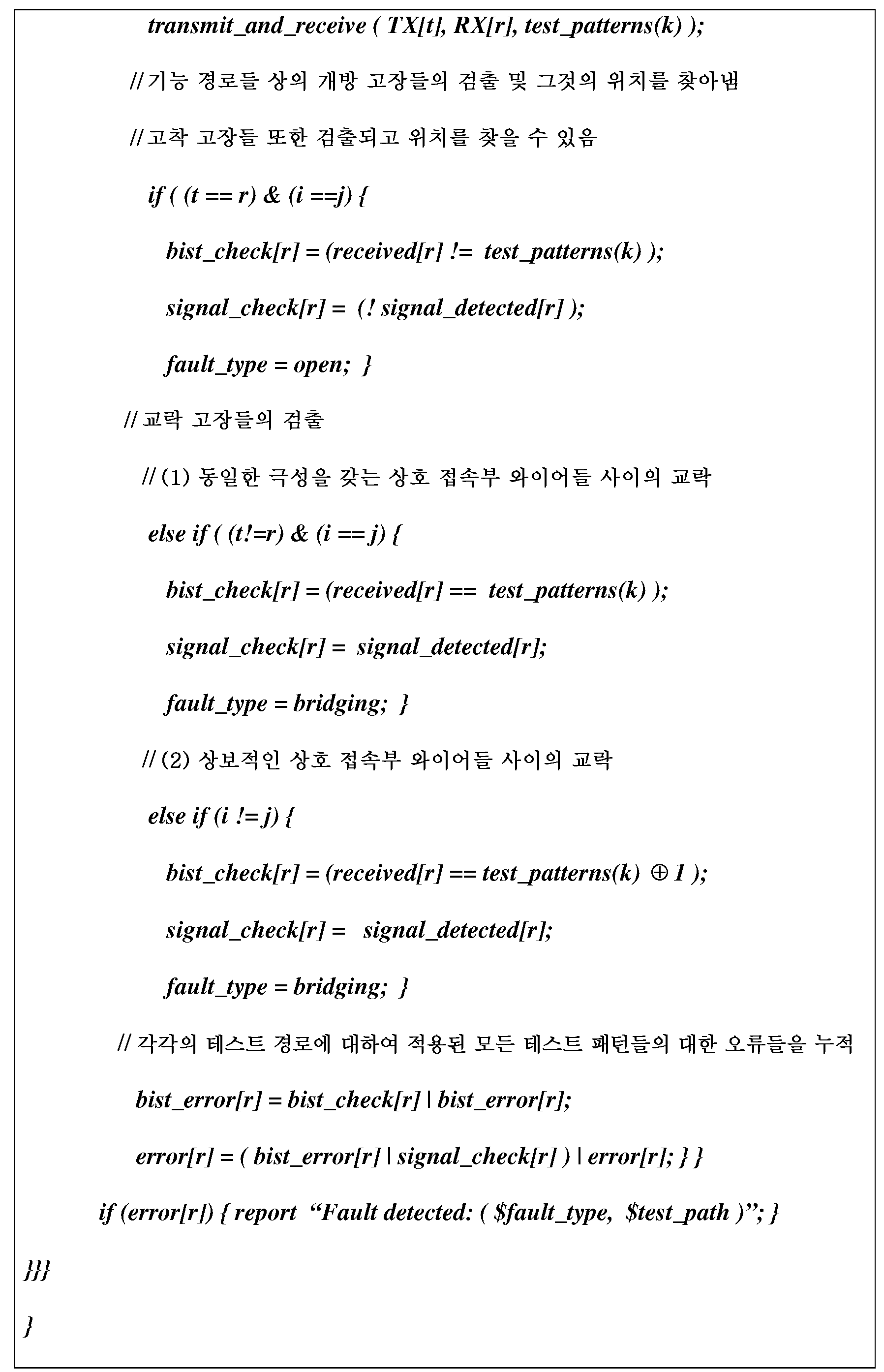
<개방 및 교락 테스트 프로시저><Opening and Interrogation Test Procedure>
개방 고장들은 (t=r)&(i=j)인 경우에 기능 경로 (tsw[t,i],rsw[r,j])를 통하여 테스트될 수 있다. 변수 fault_type은 검출된 고장의 유형을 계속 추적하기 위해 이용될 수 있다. 만일 개방 고장이 검출되면, 개방 고장은 fault_type에 할당된다. 테스트 결과는 대응하는 테스트 경로에서 검출된 고장 유형을 나타내는 (fault_type, test path) ∈ DET의 형태로 수집될 수 있다.Open faults can be tested through the functional path tsw [t, i], rsw [r, j] if (t = r) & (i = j) The variable fault_type can be used to keep track of the type of fault detected. If an open fault is detected, the open fault is assigned to fault_type. The test results may be collected in the form of (DET_TYPE, TEST path) ∈ DET indicating the type of fault detected in the corresponding test path.
교락 고장들을 검출하는 테스트 경로들의 세트는 유사하게 ![]()
![]()
가격 경쟁력을 포함하는 문제들에 대처하기 위하여, 시스템 보드 제조자들은 보다 작은 보드에 보다 많은 시스템 기능들을 통합하려는 노력을 증가시켰다. 그러나, 이러한 통합 목적을 달성하기 위해 의도된 보드 설계 노력은 불행하게도 감소된 상호 접속부 와이어 치수들 및 상호 접속부 와이어들에 대한 보다 타이트한 라우팅 제약으로 귀결되고, 이는 근처의 상호 접속부 와이어들 사이의 혼선을 악화시킬 수 있다. 혼선에 의해 야기된 신호 무결성 문제는 지터를 증가시킬 수 있고, 이는 수신기에서의 데이터 복구를 어렵게 만들 수 있다. 혼선의 검출 및 분석은 일반적으로 성가시기 때문에, 혼선의 소스들을 찾아낼 수 있는 테스트 방법들의 이용 가능성은 양 증가(volume ramp up) 및 시스템 보드들의 유효성 검사에 결정적일 수 있다.In order to cope with problems including price competitiveness, system board manufacturers have increased their efforts to integrate more system functions into smaller boards. However, the board design effort intended to achieve this integration objective unfortunately results in reduced interconnecting wire dimensions and tighter routing constraints on the interconnect wires, which can lead to cross talk between nearby interconnect wires It can aggravate. Signal integrity problems caused by crosstalk can increase jitter, which can make data recovery at the receiver difficult. Since detection and analysis of crosstalk is generally cumbersome, the availability of test methods that can detect sources of crosstalk can be crucial to volume ramp up and validation of system boards.
일부 실시예들에서, 위에 설명된 것과 같은 교락에 대한 테스트 방법이 HSIO 상호 접속부들 사이의 혼선을 찾아내기 위해 적용될 수 있다. 도 12는, 송신기(1210)로부터 수신기(1220)로의 회로(1200)와, 송신기(1260)로부터 수신기(1270)로의 회로(1250) 사이와 같은, 혼선의 검출을 위한 시스템의 실시예의 예시이다. 혼선은 도 12의 회로(1200)와 회로(1250) 사이에 도시된 예로서 결합 커패시터(1225)로 교락 고장을 대체하는 것에 의해 모델링될 수 있다. Cc로서 표시된 결합 커패시터(1225)는 혼선에 의해 야기된 결합 노이즈를 모델링하기 위해 제공된다. 결합 노이즈는 교락 고장의 일반적인 경우로 간주될 수 있는데, 이는 교락 고장의 효과가 Cc=∞에 의해 근사해질 수 있기 때문이다.In some embodiments, a test method for interlaced as described above can be applied to find the cross talk between HSIO interconnects. 12 is an illustration of an embodiment of a system for detection of crosstalk, such as between
일부 실시예들에서, 위에 설명된 테스트 프로시저는 혼선을 찾아내기 위해 이용될 수 있다. 만일 테스트 패턴이 TX[t+d]로부터 테스트 경로 (tsw[t+d,0],rsw[t,1])을 통하여 적용된다면, Cc가 충분히 큰 경우에 결과로서 혼선이 생길 수 있다. 테스트 경로가 확립될 때, 테스트 경로는, 직렬로, 커패시터들 Cc 및 C와 AC 결합될 수 있다. Cc<<C가 일반적으로 가정되므로, AC 결합된 테스트 경로의 총 커패시턴스는 Cc에 의해 지배될 수 있다. 만일 Cc가 충분히 크다면, 입력 테스트 패턴은 테스트 경로를 통하여 전송될 수 있고 신호 검출기 또는 오류 체크기에 의해 싱크에서 검출될 수 있다.In some embodiments, the test procedure described above can be used to detect crosstalk. If the test pattern is applied from the TX [t + d] through the test path tsw [t + d, 0], rsw [t, 1], the result may be crosstalk if C c is large enough. When the test path is established, the test path may be AC coupled with the capacitors C c and C in series. Since C c << C is generally assumed, the total capacitance of the AC coupled test path can be dominated by C c . If C c is large enough, the input test pattern can be transmitted through the test path and detected in the sink by a signal detector or error checker.
일부 실시예들에서, 결합 노이즈의 진폭은 테스트 파형의 주파수 및 진폭에 의존하기 때문에, 최대 주파수를 제공하는 테스트 파형 '1010...10'(또는 '0101...01')의 최대 진폭은 혼선 테스트를 위해 이용될 수 있다. 일부 실시예들에서, 테스트 파형의 진폭은 등화(equalization)에 의해 증폭될 수 있다. 등화는 모든 신호 천이에서 신호 진폭을 증대하는 시스템 함수이다. 대안적으로, 동일한 테스트 파형의 진폭은 원하는 증폭 계수에 의해 증가될 수 있다. 증폭 계수는 신호 검출기 임계치 및 혼선 임계치로부터 결정될 수 있다. 예를 들어, 만일 신호 검출기 임계치가 50mV이고 혼선 임계치가 40mV이면, 입력 테스트 파형은 신호 검출기에서 바람직하지 않은 결합 노이즈가 검출될 수 있는 지점까지 증폭될 수 있다.In some embodiments, since the amplitude of the coupling noise depends on the frequency and amplitude of the test waveform, the maximum amplitude of the test waveform '1010 ... 10' (or '0101 ... 01') providing the maximum frequency is Can be used for crosstalk testing. In some embodiments, the amplitude of the test waveform may be amplified by equalization. Equalization is a system function that increases the signal amplitude at all signal transitions. Alternatively, the amplitude of the same test waveform can be increased by the desired amplification factor. The amplification factor may be determined from the signal detector threshold and the crosstalk threshold. For example, if the signal detector threshold is 50 mV and the crosstalk threshold is 40 mV, then the input test waveform can be amplified to the point where undesirable coupling noise can be detected in the signal detector.
일부 실시예들에서, 동일한 테스트 프로시저가 혼선 및 교락 고장의 검출에 적용될 수 있기 때문에, 혼선은 교락 테스트 동안에 표적이 된다. 이것은 결합 고장을 자극하는 입력 테스트 파형의 진폭을 교정(calibrating)하는 것에 의해 수행될 수 있다. 혼선을 교락 고장으로부터 구별하기 위하여, 입력 파형에서 진폭 및/또는 천이의 수를 감소시키는 것에 의해 보다 상세한 분석이 수행될 수 있다. 전술한 바와 같이, 결합 노이즈는 입력 테스트 파형의 진폭 및 천이의 수(즉, 주파수)에 의존하고 이들 인자들이 감소될 때 점차 희미해질 수 있다(fade out). 따라서, 만일 천이의 수 및 진폭의 감소 후에 오류가 사라진다면, 결합 노이즈로 결론지어질 수 있다. 그러나, 이들 신호 수정들에도 불구하고 오류가 지속하면, 얼마간의 오류의 마진 내에서, 교락 고장으로 결론지어질 수 있다.In some embodiments, crosstalk is targeted during the interlacing test, since the same test procedure can be applied for detection of crosstalk and entanglements failure. This can be done by calibrating the amplitude of the input test waveform to stimulate the coupling fault. A more detailed analysis can be performed by reducing the number of amplitudes and / or transitions in the input waveform to distinguish the crosstalk from entangled faults. As described above, the coupling noise is dependent on the amplitude and the number of transitions (i. E., Frequency) of the input test waveform and may fade out as these factors are reduced. Thus, if the error disappears after the number of transitions and the decrease in amplitude, then a coupling noise can be concluded. However, if the error persists despite these signal modifications, within some margin of error, an interlaced failure can be concluded.
일부 실시예들에서, 고장 검출을 위해, 병렬로 모든 송신기들 및 수신기들에 의해 고장 테스트가 수행될 수 있다. 병렬 테스트 접근법은 감소된 테스트 시간 때문에 테스트 비용 절약을 제공할 수 있다. 개방 고장들 및 교락 고장들에 대한 병렬 테스트의 예가 표 4 및 5에 각각 제공되어 있다. 병렬 테스트는 전술한 바와 같이 고착 테스트 후에 수행되는 것으로 가정된다.In some embodiments, for fault detection, a fault test may be performed by all transmitters and receivers in parallel. The parallel test approach can provide test cost savings due to reduced test time. Examples of parallel tests for open faults and cross-link faults are provided in Tables 4 and 5, respectively. The parallel test is assumed to be performed after the adhesion test as described above.

<병렬 개방 테스트 프로시저><Parallel Open Test Procedure>
병렬 개방 테스트 프로시저에서, '101010...10'의 테스트 패턴이 가정된다. controls에서 제공된 스위치 제어 입력들에 의해 확립된 2개의 테스트 경로가 있을 수 있다. 동일한 제어 입력이 모든 r에 대하여 txc[r,1:0] 및 rxc[r,1:0]에 제공될 수 있다. 도 13은 개방 고장 검출의 실시예를 예시한다. 도 13은 송신기(1310)로부터 수신기(1320)로의 회로(1300) 및 송신기(1360)로부터 수신기(1370)로의 회로(1350)를 예시한다. 도 13에 예시된 예에서, controls[0][3:0] 또는 controls[0] = '0101'(또는 controls[1] = '1010')은 포지티브(또는 네거티브) 상호 접속부 와이어들 상의 개방 고장을 검출하기 위한 테스트 경로를 확립하기 위해 이용될 수 있다. 이 예시에서, 개방 고장(1315)은 회로(1300)의 포지티브 상호 접속부 상에 도시되어 있고, 개방 고장(1365)은 회로(1350)의 네거티브 상호 접속부 상에 도시되어 있다. 개방 테스트는 기능 경로 상에서 실행될 수 있기 때문에, 만일 전송된 테스트 패턴이 수신되지 않으면, 또는 만일 수신기에서 어떤 AC 신호도 검출되지 않으면 오류가 검출될 수 있다. 오류는 (fault_type,(r,controls[i]))의 형태일 수 있다. 테스트 경로 (tsw[r,i],rsw[r,j])는 (r,controls[i])와 동등한데, 이는 controls[i]는 TX[r]와 RX[r]을 접속하여 형성된 link[r] 내의 스위치들 tsw[r,i] 및 rsw[r,i]를 턴 온시키기 때문이다.In the parallel open test procedure, a test pattern of '101010 ... 10' is assumed. There may be two test paths established by the switch control inputs provided in the controls. The same control input may be provided for txc [r, 1: 0] and rxc [r, 1: 0] for all r. Figure 13 illustrates an embodiment of open fault detection. 13 illustrates a
기능 신호 경로들을 차단할 수 있는 개방 고장들과 대조하여, 교락 고장들은 추가적인 바람직하지 않은 비기능 신호 경로들을 도입할 수 있다. 일부 실시예들에서, 아래에 설명된 병렬 교락 테스트 프로시저는 교락 고장들에 의해 생성된 비기능 신호 경로들을 검출하기 위해 제공된다. 교락 고장들에 대한 스위치 제어 입력들은 비기능 경로들을 통하여 테스트 경로들을 확립하기 위해 이용될 수 있다. 교락 고장들은 상이한 링크들을 가로질러 임의의 상호 접속부 와이어들을 단락(short)시킬 수 있다. 교락 고장은 양쪽 모두 동일한 극성을 갖는 또는 상보적인 극성을 갖는 상호 접속부 와이어들 사이에 비기능 경로들을 도입할 수 있다.In contrast to open faults that can block functional signal paths, chirping faults can introduce additional undesired non-functional signal paths. In some embodiments, the parallel interlacing test procedure described below is provided for detecting non-functional signal paths generated by interlaced failures. The switch control inputs to the chatter faults can be used to establish test paths through the non-functional paths. The chirping faults can short-circuit any interconnect wires across different links. The interlocking fault can introduce non-functional paths between interconnection wires, both having the same polarity or having complementary polarity.
일부 실시예들에서, 교락 고장들은 모든 스위치들이 닫힌 상태로 각각의 채널 링크에 테스트 패턴을 적용하는 것에 의해 검출될 수 있다. 테스트 구조의 실시예에서, 이것은 각각의 TX로부터 상이한 패턴들이 생성될 수 있다면, 요구되는 제어 입력을 '1010' 및 '0101'로부터 '1101' 및 '1110'으로 변경하는 것에 의해 위에 설명된 개방 테스트 프로시저에 통합될 수 있다. 개방 테스트 프로시저 내의 controls는, 교락 테스트가 통합될 때, controls = ('1110','1101')일 수 있다. 모든 링크들에 대한 최초의 테스트 구성들, 즉, '1010' 및 '0101'은 개방 고장들의 진단을 위해 이용될 수 있다.In some embodiments, entanglements failures can be detected by applying a test pattern to each channel link with all switches closed. In an embodiment of the test structure, this may be achieved by changing the required control input from '1010' and '0101' to '1101' and '1110', if the different patterns can be generated from each TX, Can be integrated into the procedure. The controls within the open test procedure can be controls = ('1110', '1101') when the interlocking test is integrated. The initial test configurations for all links, i.e., '1010' and '0101', can be used for diagnosis of open faults.
만일 각각의 TX에서 모든 스위치들이 닫힌다면, 교락 고장들은, 특히 차동 상호 접속부 와이어들 중 하나만이 개방인 경우에, 테스트 패턴 파형들이 수신기에서 성공적으로 복구되지 않도록 그것들이 간섭되거나 왜곡되게 할 수 있다. 따라서, 결과로서 오류가 생길 수 있고 BIST 하드웨어에 의해 검출될 수 있다. 디스에이블된 RX 상호 접속부는 교락 고장들이 존재할 때 데이터 복구가 일어나지 않는 것을 보증하기 위해 이용될 수 있다. RX에서 이러한 구현이 없이, 예를 들면, 도 3에 도시된 바와 같이 하나의 링크의 상호 접속부 및 이웃 링크의 상보적인 상호 접속부와 같은, 링크들 사이의 상보적인 상호 접속부들에서 그러한 교락 고장들이 발생한다면 테스트 패턴 파형의 소거(calcellation)에 의해 교락 고장들이 마스킹되는 위험이 있을 수 있다.If all switches in each TX are closed, the chirping faults can cause them to interfere or distort, especially if only one of the differential interconnect wires is open so that the test pattern waveforms are not successfully recovered at the receiver. As a result, errors may result and be detected by the BIST hardware. The disabled RX interconnect can be used to ensure that no data recovery occurs when chirality faults are present. Without such an implementation in RX such bridging faults occur in complementary interconnections between links, such as, for example, the interconnections of one link and the complementary interconnections of neighboring links, as shown in Figure 3 There is a risk that the chatter faults are masked by the calcellation of the test pattern waveform.
일부 실시예들에서, 만일 테스트를 받는 모든 링크들에 대한 상이한 테스트 패턴이 테스트에 대하여 이용 가능하다면, 교락 고장 검출은 2개의 테스트 실행들에서 또는 2개의 테스트 구성들, 모든 r에 대하여 rsw[r,0]가 닫힌 제1 실행과 rsw[r,1]이 닫힌 제2 실행으로 달성될 수 있다. 따라서, 테스트의 복잡도는 ![]()
![]()
일부 실시예들에서, 고장 검출에서 사용되는 상이한 테스트 패턴들은 의사랜덤 테스트 패턴 생성기(pseudorandom test pattern generator)로부터 얻어질 수 있다. 의사랜덤 테스트 패턴은 기능 테스트에서 일반적으로 이용되고, 의사랜덤 바이너리 시퀀스(PRBS) 패턴 생성기를 이용하여 생성될 수 있다. PRBS 패턴 생성기는 일반적으로 특정한 생성 다항식에 기초한다. 최초 상태로부터 시작하여, 생성기는 시퀀스가 반복하기 전에 ![]()
![]()
도 14는 교락 고장 검출의 실시예의 예시이다. 이 예시는 고장들 b0, b1, b2, 및 b3로서 도시된, 다수의 교락 고장들을 포함할 수 있는 3개의 회로들(회로들(1400, 1425, 및 1450))의 예를 포함한다. 만일 도 14에 도시된 테스트 구성들이 개방 고장 테스트를 위해 이용된다면, 교락 테스트는 개방 테스트와 오버랩될 수 있다. 테스트 구성들 '1101' 및 '1110'에 의해 확립된 테스트 경로들 내의 열린 스위치들은 교락 고장 마스킹을 감소시키기 위해 이용될 수 있다. 고장 마스킹은 다수의 교락 고장들이 상보적인 상호 접속부 와이어들 중 하나 내의 테스트 패턴 파형을 사라지게 할 때 일어날 수 있고 그 테스트 패턴 파형은 남아 있는 상호 접속부 경로를 통해 복구될 수 있다. 대안적인 신호 전파 경로를 디스에이블하는 것에 의해, 교락 고장은 검출될 수 있다.14 is an example of an embodiment of interlaced fault detection. This example includes an example of three circuits (
일부 실시예들에서, 교락 고장들에 대한 상호 접속부 테스트는 controls = ('1001','0110')에 의해 확립된 이전에 논의된 상보적인 테스트 구성들과 함께 임의의 2개의 이용 가능한 테스트 패턴들을 이용해 수행될 수 있다. 바람직한 테스트 패턴들은 '1010...10' 및 그것의 비트 단위 보수인 '0101...01'이지만 대안으로 테스트 패턴들의 쌍, 바람직하게는 최대 수의 천이들을 포함하는 패턴들이 BIST 하드웨어에서 이용 가능한 테스트 패턴들로부터 선택될 수 있다. 아래에 논의되는 병렬 상호 접속부 테스트 접근법에 적용될 수 있는, 2개의 바람직한 상보적인 테스트 패턴들 및 상보적인 테스트 구성의 이들 간단한 요건들은 제조 보드 테스트를 위한 실행 가능한 명세를 제공하기 위해 이용될 수 있다. 만일 테스트 구조들 및 2개의 바람직한 상보적인 테스트 패턴들이 테스트를 받는 보드 상의 각각의 IC 디바이스에서 이용 가능하게 된다면, HSIO 상호 접속부 테스트는 병렬로 수행될 수 있다.In some embodiments, the interconnection test for interlaced faults is performed with any two available test patterns, with the previously discussed complementary test configurations established by controls = ('1001', '0110' ≪ / RTI > The preferred test patterns are '1010 ... 10' and its bitwise complement '0101 ... 01', but alternatively patterns comprising a pair of test patterns, preferably the maximum number of transitions, are available in the BIST hardware Can be selected from the test patterns. Two preferred complementary test patterns and these simple requirements of a complementary test configuration, which may be applied to the parallel interconnect test approach discussed below, can be used to provide a viable specification for manufacturing board testing. If test structures and two preferred complementary test patterns are made available to each IC device on the board under test, the HSIO interconnect test may be performed in parallel.
테스트 방법의 실시예에서, 상보적인 상호 접속부 와이어들 상의 교락 고장들이 먼저 표적이 될 수 있는데, 이는 이들 고장들이, 예를 들면, 도 7에서 도시된 제안된 테스트 구성으로부터 검출될 수 있기 때문이다. 그러나, 도 7에 도시된 테스트 구성으로부터 모든 교락 고장들이 다 검출되지 않을 수 있다. 예를 들면, 동일한 극성을 갖는 상호 접속부 와이어들 상의 교락 고장들은 도 7의 테스트 구성에서 검출되지 않을 것이다. 검출되지 않은 교락 고장들을 포함하는 동일한 극성을 갖는 상호 접속부 와이어들은 상보적인 상호 접속부 와이어들에 대한 교락 테스트 환경이 적용될 수 있도록 스위치 제어들 및 테스트 패턴들을 구성하는 것에 의해 상보적인 상호 접속부 와이어들로 변환될 수 있다. 그 변환들은 그 후 모든 교락 고장들이 검출될 때까지 연속적으로 적용될 수 있다.In an embodiment of the test method, entanglement faults on complementary interconnection wires can be targeted first because these faults can be detected, for example, from the proposed test configuration shown in Fig. However, not all bridging faults may be detected from the test configuration shown in Fig. For example, entanglement faults on interconnect wires having the same polarity will not be detected in the test configuration of FIG. The interconnection wires having the same polarity including undetected interlock failures are converted to complementary interconnection wires by configuring the switch controls and test patterns so that the interlace test environment for the complementary interconnection wires can be applied . The transforms can then be applied successively until all entanglement faults are detected.
일부 실시예들에서, 상보적인 와이어들 상의 교락 고장들을 테스트하는 병렬 접근법은, 스위치 제어 값들 및 오류 검출 기준들을 제외하고는, 위에 설명된 병렬 개방 테스트와 동일하거나 유사할 수 있다. 주어진 스위치 제어 값들 '1001' 및 '0110'은 도 7에 예시된 테스트 경로들을 확립할 수 있다. 일부 실시예들에서, 오류 검출 기준들 및 오류 보고는 상호 접속부 고장들의 검출을 위해 위에 설명된 테스트 프로시저에서 논의된 것들과 유사할 수 있다. 오류는 수신된 테스트 패턴이 전송된 테스트 패턴의 보수라는 사실에 적어도 부분적으로 기초하여 결정될 수 있다.In some embodiments, the parallel approach of testing for chirping faults on complementary wires may be the same or similar to the parallel open test described above, except for switch control values and error detection criteria. The given switch control values '1001' and '0110' may establish the test paths illustrated in FIG. In some embodiments, the error detection criteria and the error report may be similar to those discussed in the test procedure described above for detection of interconnect faults. The error may be determined based at least in part on the fact that the received test pattern is a complement of the transmitted test pattern.
도 15는 상보적인 교락 고장 검출의 실시예의 예시이다. 교락 고장들은 controls[0][3:0] = '0110'에 의해 구성된 테스트 경로들에서 검출될 수 있다. 이 구현에서, txc[r,1:0]^rxc[r,1:0] = controls[0][r,3:0]이고, 여기서 기호 ^는 연쇄를 표시한다. 만일 예시된 회로들(1510(송신기(1540) 및 수신기(1570)), 1520(송신기(1550) 및 수신기(1580)), 1530(송신기(1550) 및 수신기(1590)))에 대하여 도 15에 도시된 바와 같이 테스트 경로들이 확립된다면, 표적 교락 고장들은 수신기들에서 관찰될 수 있다. 예를 들면, 교락 고장 b0 및 b1은 수신기들 RX[r](1570) 및 RX[r+1](1580)에서 관찰될 수 있다. b2 및 b3 교락 고장들은 수신기 RX[r+2](1590)에서 관찰될 수 있다. 다수의 교락 고장들 b2 및 b3의 검출은, 만일 그것들이 동시에 일어난다면, TX[r](1540) 및 TX[r+1](1550)으로부터 RX[r+2](1590)으로의 테스트 패턴 파형 사이의 신호 간섭 때문에 더 복잡해질 수 있다. 그 신호 간섭은 TX[r](1540) 및 TX[r+1](1550)으로부터 유래된 테스트 패턴 파형들 사이의 지연에 따라서 보강(constructive) 또는 상쇄(destructive)일 수 있다. 만일 테스트 패턴 파형들이, 예를 들어, 위상이 같거나(in phase)(보강) 또는 위상이 다르다면(out of phase)(상쇄), 수신기 RX[r+2](1590)에서 관찰되는 결과 신호는 진폭이 증가될 수 있고, 또는 어떤 신호도 관찰되지 않을 수 있다. 따라서, 이 테스트 구성에서 다수의 고장들의 고장 검출은 다수의 교락 고장들로부터 생기는 전파된 파형들 사이의 위상 차이들에 의존할 수 있다. 만일 그 위상 차이들이 작다면, 고장들은 수신기에서 관찰될 수 있다.15 is an illustration of an embodiment of complementary bridging fault detection. The interlaced faults can be detected in test paths configured by controls [0] [3: 0] = '0110'. In this implementation, txc [r, 1: 0] ^ rxc [r, 1: 0] = controls [0] [r, 3: 0], where the symbol ^ denotes a chain. If the illustrated circuits 1510 (
일부 실시예들에서, 동일한 교락 고장들은 controls[1][3:0] = '1001'에 의해 확립된 상보적인 테스트 경로들에서 검출될 수 있다. 그러나, 다수의 교락 고장들 b2 및 b3는 R[r](1530) 및 R[r+1](1550)에 전파된 테스트 패턴 파형들의 진폭이 TX[r+2](1560)으로부터 제공된 최초 진폭의 절반이 되게 할 수 있다. 절반 진폭은, 구현에 따라서, 여전히 관찰될 수 있다. 그러나, 테스트 구조의 실시예가 없다면, 예를 들면, 다수의 교락 고장들 b2 및 b3가 수신기들 RX[r](1570) 및 RX[r+1](1580)에서 마스킹되는 위험이 더 커질 수 있다. 이는, 적당히 분리되어 있는 상보적인 경로가 없다면, TX[r](1540) 및 TX[r+1](1550)으로부터의 테스트 패턴들은 수신기들 RX[r](1570) 및 RX[r+1](1580)에서 각각 데이터 복구를 가능하게 만들 수 있기 때문이다.In some embodiments, the same entanglements can be detected in complementary test paths established by controls [1] [3: 0] = '1001'. However, the plurality of entangle bumps b2 and b3 cause the amplitudes of the test pattern waveforms propagated to R [r] 1530 and R [r + 1] 1550 to exceed the original amplitude Of the total. The half amplitude can still be observed, depending on the implementation. However, without an embodiment of the test structure, for example, the risk of multiple masking failures b2 and b3 being masked in receivers RX [r] 1570 and RX [r + 1] 1580 may be greater . This implies that the test patterns from TX [r] 1540 and TX [r + 1] 1550 are sent to receivers RX [r] 1570 and RX [r + (1580). ≪ / RTI >
일반적으로, 만일 상호 접속부 와이어당 다수의 교락 고장들의 수가 증가되어 결과 테스트 패턴 파형들의 진폭을 설계 명세가 허용할 것보다 아래로 떨어뜨린다면, 테스트 구성에 존재하는 다수의 교락 고장들을 마스킹하는 위험이 있을 수 있다. 그러나, 이 테스트 구성에서 검출되지 않은 다수의 교락 고장들은 아래에 설명되는 바와 같이 다른 테스트 구성들에서 검출될 수 있다.Generally, if the number of interlaced failures per interconnect wire is increased and the resulting test pattern waveforms drop below the amplitude allowed by the design specification, there is a risk of masking multiple interlaced failures present in the test configuration Can be. However, a number of entanglements failures not detected in this test configuration can be detected in other test configurations as described below.
일부 실시예들에서, 병렬 고장 검출 테스트는, 주어진 테스트 구성에서 간섭이 없는 인에이블된 테스트 패턴 소스들 및 싱크들 사이에, 주어진 테스트 구성에서, 교락 고장들이 신호 경로들을 생성하는 경우에 그 교락 고장들을 신뢰성 있게 검출하기 위해 이용될 수 있다. 테스트 패턴 소스들 및 싱크들은 그것들이 각각 하나의 싱크 및 하나의 소스에만 접속된다면 간섭이 없다고 말한다. 병렬 고장 검출은 주어진 테스트 구성 및 상보적인 테스트 구성 양쪽 모두에서 상호 접속부 고장들이 신뢰성 있게 검출된다면 그러한 고장들을 찾아낼 수 있다. 신뢰성 잇게 발견되는 다수의 교락 고장들의 예는 상호 접속부 와이어당 하나의 교락 고장을 포함할 수 있다. 만일 상호 접속부 와이어들 상의 다수의 고장들이 발견될 필요가 있다면, 위에 설명된 진단 방법이 적용될 수 있다.In some embodiments, the parallel fault detection test may be performed between the enabled test pattern sources and sinks without interference in a given test configuration, in a given test configuration, if the chirping faults generate signal paths, Can be reliably detected. Test pattern sources and sinks say that there is no interference if they are connected to only one sink and one source, respectively. Parallel fault detection can detect such faults if interconnection faults are reliably detected in both a given test configuration and a complementary test configuration. An example of multiple bridging failures found to be reliable can include one bridging fault per interconnect wire. If a number of faults on the interconnect wires need to be discovered, the diagnostic method described above can be applied.
일부 실시예들에서, 상보적인 상호 접속부 와이어들 상의 교락 고장들은 도 15에 예시된 테스트에 의해 효율적으로 검출될 수 있다. 그러나, 그러한 테스트 구성들에서 모든 교락 고장들이 다 검출되지 않을 수 있다. 예를 들면, 동일한 극성을 갖는 상호 접속부 와이어들 상에 존재하는 교락 고장들은 검출되지 않을 것이다. 검출되지 않은 교락 고장들을 다루기 위해, 그 문제를 상보적인 상호 접속부 와이어들의 테스트로 변환하는 테스트 구성들이 셋업될 수 있다.In some embodiments, entanglement faults on complementary interconnect wires can be efficiently detected by the test illustrated in FIG. However, not all bridging faults may be detected in such test configurations. For example, entanglement faults present on interconnect wires having the same polarity will not be detected. To deal with undetected bridging faults, test configurations can be set up that convert the problem into a test of complementary interconnect wires.
도 16 및 17은 동일 극성을 갖는 와이어들에 대한 교락 고장 검출의 실시예들을 예시한다. 네거티브 상호 접속부 와이어들 사이의 교락 고장 검출은 포지티브 상호 접속부 와이어들과 병렬로 동일하게 수행될 수 있기 때문에, 동일한 극성을 갖는 와이어들에 대한 교락 고장 검출은 링크들의 포지티브 상호 접속부로 예시된다. 도 16은 병렬 테스트 환경에서 동일 극성을 갖는 와이어들에 대한 교락 고장 검출의 실시예의 예시이다. 예시된 바와 같이, 교락 고장 검출은 표 5에서 제시된 테스트 알고리즘을 포함할 수 있다. 회로들(1600, 1625, 1650, 및 1675) 사이의 교락 고장들을 예시하는, 도 16에 포지티브 상호 접속부 와이어들 상의 교락 고장 검출이 도시되어 있다. 이 예시에서, 교락 고장들 b4 내지 b7과 같은 모든 교락 고장들이 도 15에 도시된 테스트 구성에서 다 검출되지 않을 수 있다. 일부 실시예들에서, 도 16에 도시된 교락 고장들 b4 및 b5는 홀수 번호의 포지티브 링크들이 네커티브 링크들로서 거동하도록 구성되는 경우, 또는 그 반대의 경우에 검출될 수 있다. 즉, 만일 link[r+1], 또는 k=0인 경우의 link[r+2k]의 포지티브(네거티브) 상호 접속부가 link[r]의 네거티브(포지티브) 상호 접속부를 에뮬레이트(emulate)하도록 구성될 수 있다면, 짝수 및 홀수 번호의 링크들 사이의 교락 고장들은 검출될 수 있다.Figures 16 and 17 illustrate embodiments of entanglement fault detection for wires having the same polarity. Since entanglement fault detection between negative interconnection wires can be performed in parallel with positive interconnection wires, entanglement fault detection for wires having the same polarity is illustrated as a positive interconnection of the links. Figure 16 is an illustration of an embodiment of bridging fault detection for wires having the same polarity in a parallel test environment. As illustrated, entanglement fault detection may include the test algorithms presented in Table 5. 16 shows an interlocking fault detection on the positive interconnection wires, illustrating interlocking faults between the
일부 실시예들에서, 변환은 도 16에 도시된 바와 같이, 상보적인 테스트 패턴 파형(또는 link[r]과 상이한 테스트 파형) 및 상보적인 스위치 제어 값들을 link[r+20]에 제공하는 것에 의해 달성될 수 있다. 이 구성에서, 교락 테스트는 도 15에 예시된 교락 테스트에서는 검출되지 않을 교락 고장들 b4 및 b5를 검출하기 위해 이용될 수 있다. 이 구현에서, 각각의 링크에 대한 스위치 제어 입력들은 동일하지 않다. link[r] 및 link[r+2]에 대한 스위치 제어들은 controls[0] = '0110'이고, 다른 링크들, link[r+1] 및 link[r+3]에 대하여, 스위치 제어들은 controls[1] = '1001'이다.In some embodiments, the conversion may be performed by providing complementary test pattern waveforms (or test waveforms different from link [r]) and complementary switch control values to link [r + 2 0 ] ≪ / RTI > In this configuration, the interlacing test can be used to detect interlaced failures b4 and b5 that will not be detected in the interlaced test illustrated in Fig. In this implementation, the switch control inputs for each link are not the same. The switch controls for link [r] and link [r + 2] are controls [0] = '0110' and for other links, link [r + 1] and link [r + 3] [1] = " 1001 ".
그러나, 도 16에 예시된 테스트 구성은 동일한 극성을 갖는 와이어들에서 모든 고장들을 검출하지 않을 수 있다. 예를 들어, 교락 고장들 b6 및 b7은 도 16에 제공된 이 테스트 구성에서 검출되지 않는다. 도 17은 병렬 테스트 환경에서 동일 극성을 갖는 와이어들에 대한 교락 고장 검출의 실시예의 예시이다. 예시된 바와 같이, 교락 고장 검출은 표 5에서 제시된 테스트 알고리즘을 이용할 수 있다. 교락 고장들 b6 및 b7을 검출하기 위하여, 동일한 변환은 link[r]의 네거티브(포지티브) 상호 접속부를 에뮬레이트하기 위해 link[r+21]의 포지티브(네거티브) 상호 접속부에 적용될 수 있고, 결국 회로들(1700, 1725, 1750, 및 1775) 사이의 교락 고장들을 예시하는, 도 17에 도시된 테스트 구성으로 귀결된다. 일부 실시예들에서, 동일한 변환은 검출되지 않은 교락 고장들을 포함하는 상호 접속부 와이어들의 쌍에 적용될 수 있다. b6 및 b7과 같은 검출되지 않은 교락 고장들을 검출할 수 있는 테스트 구성이 도 17에 도시되어 있다. 이 예시에서, 교락 고장들 b6 및 b7은 수신기들 RX[r+2] 및 RX[r+3]에서 검출될 수 있다.However, the test configuration illustrated in FIG. 16 may not detect all failures in wires having the same polarity. For example, entanglements b6 and b7 are not detected in this test configuration provided in Fig. Figure 17 is an illustration of an embodiment of interlaced fault detection for wires having the same polarity in a parallel test environment. As illustrated, entanglement fault detection can utilize the test algorithms presented in Table 5. The same transform can be applied to the positive (negative) interconnect of the link [r + 2 1 ] to emulate the negative (positive) interconnect of the link [r] to detect the interlaced failures b6 and b7, Results in the test configuration shown in Fig. 17, which illustrates interlaced failures between the
일반적으로, link[r+d]의 포지티브(네거티브) 상호 접속부는 link[r]의 네거티브(포지티브) 상호 접속부처럼 거동하도록 구성되거나 변환될 수 있고 또는 그 반대도 가능할 수 있고, 여기서 ![]()
![]()
![]()
![]()
![]()
![]()
![]()
![]()
![]()
![]()
![]()
![]()
![]()
![]()
도 18은 교락 고장을 검출하는 테스트 구성들을 예시한다. 이 예시에서, 예로서, 8개의 링크들의 상호 접속부 와이어들 상의 교락 고장들을 검출하기 위한 테스트 구성들이 제공된다. k=0 및 d = 20인 경우, 테스트는 도 16에 예시된 교락 고장들을 검출하기 위해, config[0][7:0] = '10101010'으로 표시된, 테스트 구성을 이용하여 수행될 수 있다. 테스트는 k=1 및 2, d=21 및 d=22에 대하여, 도 17에 예시된 대응하는 config[1] = '11001100' 및 config[2] = 11110000을 이용하여 계속될 수 있다. 도 15에 예시된 테스트 구성 config[3] = 00000000은 각 링크 내의 교락 고장들을 검출하기 위해 이용될 수 있다. 일부 실시예들에서, 교락 고장들과 결합된 개방 고장을 찾아내기 위해 테스트 구성들의 비트 단위 보수가 사용될 수 있다. k=0,1,2,3에 대한 config[k]의 비트 단위 보수는 각각 01010101, 00110011, 00001111 및 11111111일 수 있다. 일찍이 논의된 바와 같이, 개방 고장들의 위치, 즉 교락 고장의 왼쪽 또는 오른쪽을 식별하기 위해 개방 고장 검출로부터의 결과들과 상보적인 DET 내의 비대칭 교락 고장 검출이 이용될 수 있다. 일부 실시예들에서, 복잡한 다수의 교락 고장들은 진단 분해능이 증가될 수 있도록 각각의 테스트 구성에서 보다 단순한 교락 고장들에 투영될 수 있다.Figure 18 illustrates test configurations for detecting intrusion failure. In this example, as an example, test configurations are provided for detecting interlaced failures on interconnect wires of eight links. If k = 0 and d = 2 0 , the test can be performed using the test configuration, indicated by config [0] [7: 0] = '10101010', to detect the interlock faults illustrated in FIG. . The test can continue with k = 1 and 2, d = 2 1 and d = 2 2 using the corresponding config [1] = '11001100' and config [2] = 11110000 illustrated in FIG. The test configuration config [3] = 00000000, illustrated in FIG. 15, can be used to detect bridging faults in each link. In some embodiments, a bitwise complement of test configurations may be used to find open faults coupled with cross-link failures. The bitwise complement of config [k] for k = 0, 1, 2, 3 may be 01010101, 00110011, 00001111 and 11111111, respectively. As discussed earlier, asymmetric intermix fault detection in DET that is complementary to the results from open fault detection can be used to identify the location of open faults, i. E., Left or right of an interlock fault. In some embodiments, complex multiple entanglement failures can be projected to simpler entangle failures in each test configuration so that diagnostic resolution can be increased.
각각의 링크에 대한 스위치 제어 입력들은 controls[i]에서 인덱스 i의 값으로서 표시된다. 만일 임의의 링크들의 쌍이 i≠j에 대하여 contols[i] 및 controls[j]로 구성된다면, 하나의 링크에 적용된 테스트 패턴은 다른 것의 비트 단위 보수일 수 있다.The switch control inputs for each link are indicated as the value of index i in controls [i]. If a pair of arbitrary links consists of contols [i] and controls [j] for i? J, the test pattern applied to one link may be a bitwise complement of the others.
만일 도 16 및 17의 테스트 구성들이 이진수들의 칼럼들로서 해석된다면, 조합된 칼럼들은 0으로부터 22-1까지의 순서화된 수들의 이진수 표현을 제공한다. 즉, 00, 01, 10, 및 11은 각각 0, 1, 2, 및 3의 이진수 표현들이다. 반대로, 만일 링크마다의 기초 상보 능력(per-link basis complementation capability)을 갖는 BIST 하드웨어를 공유하는 4개의 링크가 테스트를 받는 보드 상에 있다면, 테스트 구성들은 이진수로 표현된 0으로부터 3까지의 순서화된 수들의 칼럼들로부터 획득될 수 있다.If the test configurations of FIGS. 16 and 17 are interpreted as columns of binary numbers, the combined columns provide a binary representation of the ordered numbers from 0 to 2 2 -1. That is, 00, 01, 10, and 11 are binary representations of 0, 1, 2, and 3, respectively. Conversely, if the four links sharing the BIST hardware with per-link basis complementation capability are on the board being tested, then the test configurations are ordered from 0 to 3 expressed in binary numbers Can be obtained from the columns of numbers.
일반적으로, N개의 링크들에서 동일한 극성을 갖는 상호 접속부 와이어들을 테스트하기 위한 테스트 구성들은 이진수로 표현된 0으로부터 N-1까지의 순서화된 수들의 칼럼들로부터 획득될 수 있다. 예를 들면, 8개의 링크의 테스트 구성들은 이진수, 즉, 000, 001, 010, 011, 100, 101, 110, 및 111로 순서화된 수들 0 내지 7로부터 획득될 수 있다. 요구되는 테스트 구성들은 도 18에 예시된 이진수들의 칼럼들로부터 획득될 수 있다. 동일한 극성을 갖는 상호 접속부 와이어들을 테스트하기 위한 ![]()
![]()
병렬 교락 테스트의 실시예가 표 5에 요약되어 있다.Examples of the parallel entanglements test are summarized in Table 5.


<병렬 교락 테스트 프로시저><Parallel Jam Test Procedure>
전술한 바와 같이, ![]()
![]()
![]()
![]()
![]()
![]()
일부 실시예들에서, 포지티브 상호 접속부 와이어들 사이의 및 네거티브 상호 접속부 와이어들 사이의 교락 고장들은 동일한 테스트 구성들을 이용하여 병렬로 표적이 될 수 있다. 따라서, 제안된 교락은 0부터 ![]()
![]()
![]()
![]()
전체 제안된 병렬 테스트의 테스트 복잡도도 ![]()
![]()
![]()
![]()
도 19는 상호 접속부 고장 검출의 실시예를 예시하는 순서도이다. 이 예시에서, 테스트될 회로들이 식별되고(1902) 하나 이상의 고장 상태들에 대하여 수행될 테스트들이 결정된다(1904). 예를 들면, 개방 고장, 교락 고장, 고착 고장, 또는 혼선 고장 테스트 중 하나 이상에 대하여 테스트들이 계획될 수 있다. 또한, 테스트는 그러한 고장들의 조합에 대한 것일 수 있고, 병렬로 다수의 회로들을 테스트할 수 있다. 만일 고장 검출을 위한 신호 경로들(또는 테스트 경로들)을 확립하는 스위치들을 포함하거나 지원하는 것과 같이, 고장 검출을 위하여 회로의 송신기 및 수신기 양쪽 모두가 인에이블된다면(1906), 상호 접속부의 송신기 및 수신기 측들의 스위치들에 대하여 제어 신호들이 확립된다(1908). 만일 송신기 및 수신기가 고장 검출을 위해 양쪽 모두 인에이블되지 않는다면(즉, 고장 검출을 위해 송신기 또는 수신기만이 인에이블된다면), 인에이블되는 송신기 또는 수신기의 스위치들에 대하여 제어 신호들이 확립된다(1910).19 is a flow chart illustrating an embodiment of interconnect fault detection. In this example, the circuits to be tested are identified 1902 and the tests to be performed on one or more fault conditions are determined 1904. For example, tests can be planned for one or more of open failure, entanglement failure, sticking failure, or cross talk failure test. The test may also be for a combination of such faults and may test multiple circuits in parallel. If both the transmitter and the receiver of the circuit are enabled (1906) for fault detection, such as including or supporting switches that establish signal paths (or test paths) for fault detection, Control signals are established for the switches on the receiver sides (1908). If both the transmitter and the receiver are not enabled for fault detection (i.e., only the transmitter or receiver is enabled for fault detection), control signals are established for the enabled transmitter or receiver switches 1910 ).
제어 신호들은 그 후 테스트 구조의 적절한 스위치들에 적용되고(1912), 고장 검출을 위한 테스트 구조에 따라서, 테스트를 받는 회로들의 송신기들에 테스트 패턴들이 적용된다(1914). 테스트 패턴 신호들은 그 후 테스트를 받는 회로들의 수신기들에서 수신될 수 있고(1916), 그러한 수신된 신호들은 고장들을 나타내는 하나 이상의 오류를 잠재적으로 포함한다. 다른 실시예들에서, 테스트 패턴 신호들은 요구되는 신호들을 제공하는 테스터를 이용하여 회로들의 수신기들에 직접 적용될 수 있다. 만일 기대되는 신호들이 수신기들에서 수신된다면(어떤 오류도 검출되지 않는다면)(1918), 검출된 고장이 없다고 결론지어질 수 있다(1920). 만일 기대되는 신호들이 수신되지 않는다면(하나 이상의 오류가 검출된다면), 하나 이상의 회로에서 하나 이상의 고장이 검출되었다고 결론지어질 수 있다(1922). 그 후 시스템은 검출된 고장들의 본질을 결정하고(1924), 그것은 다수의 테스트들의 결과들을 조합하는 것을 포함할 수 있다. 그 후 프로세스는, 테스트를 받는 회로들에 대하여 요구되는, 다른 고장 상태들의 테스트를 위해 프로세스를 반복하는 것으로 계속될 수 있다(1926).The control signals are then applied 1912 to appropriate switches of the test structure and test patterns are applied 1914 to the transmitters of the circuits under test according to the test structure for fault detection. The test pattern signals can then be received 1916 at the receivers of the circuits under test, and such received signals potentially contain one or more errors indicative of failures. In other embodiments, the test pattern signals may be applied directly to the receivers of the circuits using a tester that provides the required signals. If the expected signals are received at the receivers (no errors are detected) (1918), it can be concluded that there are no detected faults (1920). If the expected signals are not received (if more than one error is detected), it can be concluded that more than one failure has been detected in more than one circuit (1922). The system then determines the nature of the detected faults (1924), which may include combining the results of multiple tests. The process may then continue with repeating the process (1926) for testing of other fault conditions, which are required for the circuits under test.
도 20은 본 발명의 실시예에 포함될 수 있는 디바이스의 실시예의 예시이다. 이 예시에서, 본 설명에 관계가 없는 특정한 표준 및 잘 알려진 컴포넌트들은 도시되지 않는다. 일부 실시예들에서, 디바이스(2000)는 송신 디바이스, 수신 디바이스, 또는 양쪽 모두일 수 있다.Figure 20 is an illustration of an embodiment of a device that may be included in an embodiment of the present invention. In this example, certain standard and well-known components not relevant to the present description are not shown. In some embodiments, the
일부 실시예들에서, 디바이스(2000)는 고속 데이터 전송을 포함할 수 있는, 정보를 통신하기 위한 상호 접속부 또는 크로스바(2005) 또는 다른 통신 수단을 포함한다. 디바이스(2000)는 정보를 처리하기 위해 상호 접속부(2005)와 연결된 하나 이상의 프로세서들(2010)와 같은 처리 수단을 더 포함한다. 프로세서들(2010)은 하나 이상의 물리적 프로세서들 및 하나 이상의 논리적 프로세서들을 포함할 수 있다. 또한, 프로세서들(2010) 각각은 다수의 프로세서 코어들을 포함할 수 있다. 상호 접속부(2005)는 간소함을 위해 단일 상호 접속부로 예시되어 있지만, 다수의 상이한 상호 접속부들 또는 버스들을 나타낼 수 있고 그러한 상호 접속부들에의 컴포넌트 접속들은 변화할 수 있다. 도 20에 도시된 상호 접속부(2005)는 적절한 브리지들, 어댑터들, 또는 컨트롤러들에 의해 접속된 임의의 하나 이상의 개별 물리적 버스들, 점대점 접속들, 또는 양쪽 모두를 나타내는 추상화(abstraction)이다. 상호 접속부(2005)는, 예를 들면, 시스템 버스, PCI 또는 PCIe 버스, 하이퍼트랜스포트(HyperTransport) 또는 ISA(industry standard architecture) 버스, SCSI(small computer system interface) 버스, IIC(I2C) 버스, 또는 때때로 "파이어와이어(Firewire)로 불리는 IEEE(Institute of Electrical and Electronics Engineers) 표준 1394 버스를 포함할 수 있다. (1996년 8월 30일에 발표된, "Standard for a High Performance Serial Bus" 1394-1995, IEEE, 및 부록) 디바이스(2000)는 디바이스 A(2075) 및 디바이스 B(2080)와 같은 하나 이상의 USB 호환 디바이스들이 부착될 수 있는, USB 버스(2770)와 같은 시리얼 버스를 더 포함할 수 있다.In some embodiments, the
일부 실시예들에서, 프로세서들(2010)은 하나 이상의 가상 머신들을 지원하기 위해 이용될 수 있다. 일부 실시예들에서, 디바이스(2000)는 프로세서들(2010)에 의해 실행될 명령어들 및 정보를 저장하기 위한 메인 메모리(2020)로서 RAM(random access memory) 또는 다른 동적 저장 디바이스를 더 포함한다. 메인 메모리(2020)는 또한 프로세서들(2010)에 의한 명령어들의 실행 동안에 임시 변수들 또는 다른 중간 정보를 저장하기 위해 이용될 수 있다. RAM 메모리는 메모리 콘텐츠의 리프레싱을 요구하는 DRAM(dynamic random access memory), 및 콘텐츠의 리프레싱을 요구하지 않지만, 비용이 증가되는 SRAM(static random access memory)을 포함한다. DRAM 메모리는 신호들을 제어하는 클록 신호를 포함하는 SDRAM(synchronous dynamic random access memory), 및 EDO DRAM(extended data-out dynamic random access memory)을 포함할 수 있다. 일부 실시예들에서, 시스템의 메모리는 디바이스 내의 다수의 에이전트들에 의해 액세스 가능한, 공유 BIOS/OS 메모리와 같은, 공유 메모리를 포함할 수 있다. 디바이스(2000)는 또한 프로세서들(2010)을 위한 정적인 정보 및 명령어들을 저장하기 위한 ROM(read only memory)(2025) 또는 다른 정적인 저장 디바이스를 포함할 수 있다. 디바이스(2000)는 특정한 엘리먼트들의 저장을 위한 하나 이상의 비휘발성 메모리 디바이스들(2030)을 포함할 수 있다.In some embodiments, processors 2010 may be utilized to support one or more virtual machines. In some embodiments, the
정보 및 명령어들을 저장하기 위해 데이터 저장소(2035)가 또한 디바이스(2000)의 상호 접속부(2005)에 연결될 수 있다. 데이터 저장소(2035)는 자기 디스크, 광 디스크 및 그것의 대응하는 드라이브, 또는 다른 메모리 디바이스를 포함할 수 있다. 그러한 엘리먼트들은 함께 조합될 수 있고 또는 개별 컴포넌트들일 수 있고, 디바이스(2000)의 다른 엘리먼트들의 부분들을 이용할 수 있다. 특정한 실시예에서, 데이터 저장소(2035)는 하드 드라이브(2036)를 포함할 수 있다.Data store 2035 may also be coupled to interconnect 2005 of
디바이스(2000)는 또한 버스(2005)를 통해 최종 사용자에 정보를 표시하기 위한 액정 디스플레이(LCD), 플라스마 디스플레이, CRT(cathode ray tube) 디스플레이, 또는 임의의 다른 디스플레이 기술 등의 디스플레이(2040)에 연결될 수 있다. 일부 실시예들에서, 디스플레이(또는 프리젠테이션 디바이스)(2040)는 텔레비전 프로그래밍을 표시하기 위해 이용될 수 있다. 일부 환경들에서, 디스플레이(2040)는 입력 디바이스의 적어도 일부로서 또한 이용되는 터치스크린을 포함할 수 있다. 일부 환경들에서, 디스플레이(2040)는 텔레비전 프로그램의 오디오 부분을 포함하는 오디오 정보를 제공하기 위한 스피커와 같은 오디오 디바이스이거나 또는 그러한 오디오 디바이스를 포함할 수 있다. 정보 및/또는 명령 선택들을 프로세서들(2010)에 전달하기 위해 입력 디바이스(2045)가 상호 접속부(2005)에 연결될 수 있다. 다양한 구현들에서, 입력 디바이스(2045)는 키보드, 키패드, 터치스크린 및 스타일러스, 음성 작동 시스템, 또는 다른 입력 디바이스, 또는 그러한 디바이스들의 조합들일 수 있다. 포함될 수 있는 다른 유형의 사용자 입력 디바이스는 방향 정보 및 명령 선택들을 하나 이상의 프로세서들(2010)에 전달하고 디스플레이(2040) 상의 커서 움직임을 제어하기 위한 마우스, 트랙볼, 또는 커서 방향 키들과 같은 커서 제어 디바이스(2050)이다.
하나 이상의 통신 엘리먼트들(2055)이 또한 상호 접속부(2005)에 연결될 수 있다. 특정한 구현에 따라서, 통신 엘리먼트들(2055)은 트랜스시버, 무선 모뎀, 네트워크 인터페이스 카드, 마더보드 상의 LAN(Local Area Network), 또는 다른 인터페이스 디바이스를 포함할 수 있다. 통신 엘리먼트들(2055)은 이더넷 데이터와 같은 네트워크 데이터를 전송하기 위해 네트워크(2065)에의 접속부를 제공할 수 있다. 통신 디바이스(2055)의 사용들은 무선 디바이스들로부터의 신호들의 수신을 포함할 수 있다. 라디오 통신을 위해, 통신 디바이스(2055)는 요구되는, 임의의 다이폴(dipole) 또는 모노폴(monopole) 안테나들을 포함하는, 하나 이상의 안테나들(2058)을 포함할 수 있다. 일 실시예에서, 통신 엘리먼트들(2055)은 부적당한 액세스로부터 디바이스(2000)를 보호하는 방화벽(firewall)을 포함할 수 있다. 디바이스(2000)는 또한 파워 서플라이, 배터리, 태양 전지, 연료 전지, 또는 전력을 제공하거나 생성하기 위한 다른 시스템 또는 디바이스를 포함할 수 있는, 전력 디바이스 또는 시스템(2060)을 포함할 수 있다. 전력 디바이스 또는 시스템(2060)에 의해 제공된 전력은 요구에 따라 디바이스(2000)의 엘리먼트들에 분배될 수 있다.One or more communication elements 2055 may also be coupled to the interconnect 2005. Depending on the particular implementation, communication elements 2055 may include a transceiver, a wireless modem, a network interface card, a local area network (LAN) on the motherboard, or other interface device. Communication elements 2055 may provide a connection to
상기 설명에서는, 설명의 목적으로, 본 발명의 철저한 이해를 제공하기 위하여 다수의 특정한 세부사항들이 제시된다. 그러나, 본 발명은 이러한 특정한 세부사항들 중 일부가 없이도 실시될 수 있다는 것은 숙련된 당업자에게 명백할 것이다. 다른 사례들에서, 잘 알려진 구조들 및 디바이스들은 블록도 형태로 도시된다. 예시된 컴포넌트들 사이에 중간 구조가 있을 수 있다. 본 명세서에 설명된 또는 예시된 컴포넌트들은 예시되거나 또는 설명되지 않은 추가적인 입력들 또는 출력들을 가질 수 있다. 예시된 엘리먼트들 또는 컴포넌트들은 또한 임의의 필드들의 재정리(reordering) 또는 필드 사이즈들의 수정을 포함하여, 상이한 배열들 또는 순서들로 배열될 수 있다.In the foregoing description, for purposes of explanation, numerous specific details are set forth in order to provide a thorough understanding of the present invention. It will be apparent, however, to one skilled in the art, that the present invention may be practiced without some of these specific details. In other instances, well known structures and devices are shown in block diagram form. There may be an intermediate structure between the illustrated components. The components described or illustrated herein may have additional inputs or outputs that are not illustrated or described. The illustrated elements or components may also be arranged in different arrangements or orders, including reordering of any of the fields or modifying the field sizes.
본 발명은 다양한 프로세스들을 포함할 수 있다. 본 발명의 프로세스들은 하드웨어 컴포넌트들에 의해 수행될 수 있고 또는 컴퓨터 판독가능한 명령어들로 구현될 수 있고, 컴퓨터 판독가능한 명령어들은 그 명령어들로 프로그램된 범용 또는 특수 용도 프로세서 또는 논리 회로들로 하여금 프로세스들을 수행하게 하기 위해 이용될 수 있다. 대안적으로, 프로세스들은 하드웨어와 소프트웨어의 조합에 의해 수행될 수 있다.The present invention may include various processes. The processes of the present invention may be performed by hardware components or may be implemented as computer-readable instructions, which may cause general purpose or special purpose processors or logic programs programmed with those instructions to cause processes And to perform the same. Alternatively, the processes may be performed by a combination of hardware and software.
본 발명의 부분들은, 본 발명에 따른 프로세스를 수행하도록 컴퓨터(또는 다른 전자 디바이스들)를 프로그램하기 위해 이용될 수 있는, 컴퓨터 프로그램 명령들이 저장되어 있는 컴퓨터 판독가능한 매체를 포함할 수 있는, 컴퓨터 프로그램 제품으로서 제공될 수 있다. 컴퓨터 판독가능한 매체는, 플로피 디스켓, 광 디스크, CD-ROM(compact disk read-only memory), 및 광자기 디스크, ROM(read-only memory), RAM(random access memory), EPROM(erasable programmable read-only memory), EEPROM(electrically-erasable programmable read-only memory), 자기 또는 광 카드, 플래시 메모리, 또는 전자 명령어들을 저장하기에 적합한 다른 유형의 매체/컴퓨터 판독가능한 매체를 포함할 수 있지만, 이에 제한되지 않는다. 또한, 본 발명은 컴퓨터 프로그램 제품으로서 다운로드될 수도 있고, 프로그램은 원격 컴퓨터로부터 요청하는 컴퓨터로 전송될 수 있다.Aspects of the present invention may be embodied in a computer program product, which may include a computer readable medium having stored therein computer program instructions, which may be used to program a computer (or other electronic devices) Can be provided as a product. The computer-readable medium may be a floppy diskette, an optical disk, a compact disk read-only memory (CD-ROM), and a magneto-optical disk, read-only memory (ROM), random access memory (RAM), erasable programmable read- only memory, electrically-erasable programmable read-only memory (EEPROM), magnetic or optical card, flash memory, or any other type of media / computer readable medium suitable for storing electronic instructions Do not. Further, the present invention may be downloaded as a computer program product, and the program may be transmitted to a requesting computer from a remote computer.
본 방법들 중 다수는 그들의 가장 기본적인 형태로 설명되지만, 본 발명의 기본적인 범주에서 벗어나지 않고 본 방법들 중 임의의 방법에 프로세스들이 추가되거나 임의의 방법으로부터 프로세스들이 삭제될 수 있고 설명된 메시지들 중 임의의 메시지에 정보가 더해지거나 임의의 메시지로부터 정보가 감해질 수 있다. 다수의 추가적인 수정들 및 개조들이 이루어질 수 있다는 것은 숙련된 당업자들에게 명백할 것이다. 특정한 실시예들은 본 발명을 제한하기 위해서가 아니라 그것을 예시하기 위해 제공되었다.Although many of these methods are described in their most basic form, it is to be understood that processes may be added to or removed from any method of any of these methods without departing from the essential scope of the present invention, Information may be added to or removed from any message. It will be apparent to those skilled in the art that numerous additional modifications and adaptations can be made. The specific embodiments have been provided to illustrate rather than to limit the invention.
만일 엘리먼트 "A"가 엘리먼트 "B"에 또는 그것과 결합된다고 한다면, 엘리먼트 A는 엘리먼트 B에 직접 결합되거나 또는, 예를 들면, 엘리먼트 C를 통하여 간접적으로 결합될 수 있다. 본 명세서가 컴포넌트, 특징, 구조, 프로세스, 또는 특성 A가 컴포넌트, 특징, 구조, 프로세스, 또는 특성 B를 "초래한다(causes)"고 진술할 때, 그것은 "A"가 적어도 "B"의 부분적인 원인이지만 "B"를 초래하는 데 도움이 되는 적어도 하나의 다른 컴포넌트, 특징, 구조, 프로세스, 또는 특성이 있을 수도 있다는 것을 의미한다. 만일 본 명세서가 컴포넌트, 특징, 구조, 프로세스, 또는 특성이 포함될 수 있다("may", "might", or "could" be included)고 언급한다면, 그 특정한 컴포넌트, 특징, 구조, 프로세스, 또는 특성은 포함되는 것이 요구되지 않는다. 만일 본 명세서가 하나의("a" 또는 "an") 엘리먼트를 언급한다면, 이것은 설명된 엘리먼트가 하나만 있다는 것을 의미하지 않는다.If element "A" is said to be associated with or with element "B ", then element A may be directly coupled to element B or indirectly through, for example, When the specification states that a component, feature, structure, process, or characteristic A is "causing" a component, feature, structure, process, or characteristic B, it means that "A" Means that there may be at least one other component, feature, structure, process, or characteristic that is a cause but contributes to a "B ". If the specification concludes with a reference to a component, feature, structure, process, or characteristic ("may", "might", or " Is not required to be included. If the specification refers to an element ("a" or "an"), it does not mean that there is only one element described.
실시예는 본 발명의 구현 또는 예이다. 본 명세서에서 "실시예", "일 실시예", "일부 실시예들", 또는 "다른 실시예들"에 대한 언급은 그 실시예들과 관련하여 설명된 특정한 특징, 구조, 또는 특성이 적어도 일부 실시예들에 포함되지만, 반드시 모든 실시예들에 포함되는 것은 아님을 의미한다. "실시예", "일 실시예", 또는 "일부 실시예들"의 다양한 출현들은 반드시 모두가 동일한 실시예들을 언급하는 것은 아니다. 본 발명의 예시적인 실시예들에 대한 앞의 설명에서, 본 명세를 능률화하고 다양한 발명의 양태들 중 하나 이상의 양태의 이해를 돕기 위해 본 발명의 다양한 특징들은 때때로 단일 실시예, 도면, 또는 그에 대한 설명에서 함께 그룹화된다는 것을 알아야 한다.Embodiments are implementations or examples of the present invention. Reference herein to "an embodiment "," an embodiment, "" some embodiments, " or" other embodiments "means that a particular feature, structure, or characteristic described in connection with the embodiments Is included in some embodiments, but is not necessarily included in all embodiments. The various appearances of "an embodiment "," one embodiment ", or "some embodiments" In the foregoing description of exemplary embodiments of the present invention, various features of the invention are sometimes incorporated into a single embodiment, a diagram, or a combination thereof, to streamline the specification and to aid in understanding one or more aspects of various inventive aspects. It should be noted that the descriptions are grouped together.
Claims (39)
송신기와 수신기 사이의 상호 접속부(interconnection)에 대한 테스트 패턴을 제공하는 테스트 패턴 소스 - 상기 송신기는 차동 출력(differential output)을 갖고, 상기 수신기는 차동 입력(differential input)을 갖고, 상기 상호 접속부는 송신기 단 및 수신기 단을 갖고, 상기 상호 접속부는 상기 송신기의 상기 차동 출력의 제1 출력 노드를 상기 수신기의 상기 차동 입력의 제1 입력 노드에 연결하는 제1 와이어 및 상기 송신기의 상기 차동 출력의 제2 출력 노드를 상기 수신기의 상기 차동 입력의 제2 입력 노드에 연결하는 제2 와이어를 포함하고, 상기 송신기는 상기 제1 와이어 상에서 상기 테스트 패턴을 상기 수신기로 송신함 -;
상기 송신기의 상기 차동 출력의 상기 제1 출력 노드와 상기 제1 와이어 사이의 제1 접속부를 열고 닫는 제1 스위치;
상기 송신기의 상기 차동 출력의 상기 제2 출력 노드와 상기 제2 와이어 사이의 제2 접속부를 열고 닫는 제2 스위치;
상기 수신기의 상기 차동 입력의 상기 제1 입력 노드와 상기 제1 와이어 사이의 제3 접속부를 열고 닫는 제3 스위치; 및
상기 수신기의 상기 차동 입력의 상기 제2 입력 노드와 상기 제2 와이어 사이의 제4 접속부를 열고 닫는 제4 스위치;를 포함하고,
상기 고장 분석 장치는 상기 제1 스위치, 상기 제4 스위치를 닫고 상기 제2 스위치 및 상기 제3 스위치를 열어서 교락 고장(bridging fault)을 검출하도록 구성되는, 고장 분석 장치.A fault analysis apparatus comprising:
A test pattern source that provides a test pattern for an interconnection between a transmitter and a receiver, the transmitter having a differential output, the receiver having a differential input, The interconnection having a first wire connecting a first output node of the differential output of the transmitter to a first input node of the differential input of the receiver and a second wire of a second output of the differential output of the transmitter, A second wire connecting an output node to a second input node of the differential input of the receiver, the transmitter transmitting the test pattern on the first wire to the receiver;
A first switch to open and close a first connection between the first output node of the differential output of the transmitter and the first wire;
A second switch for opening and closing a second connection between the second output node of the differential output of the transmitter and the second wire;
A third switch for opening and closing a third connection between the first input node of the differential input of the receiver and the first wire; And
And a fourth switch for opening and closing a fourth connection between the second input node of the differential input of the receiver and the second wire,
Wherein the failure analysis device is configured to close the first switch, the fourth switch, and open the second switch and the third switch to detect a bridging fault.
상기 제1 스위치 및 상기 제2 스위치는 상기 송신기에 포함되는, 고장 분석 장치.The method according to claim 1,
Wherein the first switch and the second switch are included in the transmitter.
상기 상호 접속부는 HSIO(high speed input-output) 상호 접속부인, 고장 분석 장치.The method according to claim 1,
Wherein the interconnect is a high speed input-output (HSIO) interconnect.
상기 상호 접속부는 DC 결합되거나(DC-coupled) 또는 AC 결합되는(AC-coupled), 고장 분석 장치.The method according to claim 1,
The interconnects may be DC-coupled or AC-coupled.
상기 제1 와이어 및 전력 소스 사이에 결합된 제1 종단 저항기 및 상기 제2 와이어 및 상기 전력 소스 사이에 결합된 제2 종단 저항기를 더 포함하고, 상기 제1 스위치는 상기 제1 와이어에 전력을 온 또는 오프시키도록 동작 가능하고, 상기 제2 스위치는 상기 제2 와이어에 전력을 온 또는 오프시키도록 동작 가능하고, 상기 제1 스위치는 상기 제1 종단 저항기를 통하여 전력을 온 및 오프시키고 상기 제2 스위치는 상기 제2 종단 저항기를 통하여 전력을 온 및 오프시키는, 고장 분석 장치The method according to claim 1,
Further comprising: a first termination resistor coupled between the first wire and the power source; and a second termination resistor coupled between the second wire and the power source, wherein the first switch powers on the first wire And the second switch is operable to turn on or off power to the second wire, the first switch being operable to turn on and off the power through the first terminating resistor, The switch turns on and off the power through the second termination resistor,
상기 송신기는 상기 수신기에 신호들을 인가하는 테스터(tester)인, 고장 분석 장치.The method according to claim 1,
Wherein the transmitter is a tester that applies signals to the receiver.
상기 송신기의 차동 출력의 제2 출력 노드와 제2 와이어 사이의 제2 접속부를 열고 닫도록 구성된 제2 스위치로서, 상기 제2 스위치를 여는 단계;
수신기의 차동 입력의 제1 입력 노드와 상기 제1 와이어 사이의 제3 접속부를 열고 닫도록 구성된 제3 스위치로서, 상기 제3 스위치를 여는 단계;
상기 수신기의 차동 입력의 제2 입력 노드와 상기 제2 와이어 사이의 제4 접속부를 열고 닫도록 구성된 제4 스위치로서, 상기 제4 스위치를 닫는 단계;
상기 제1 와이어로 테스트 패턴을 인가하는 단계;
수신된 신호들에 대하여 상호 접속부를 모니터링하는 단계; 및
상기 상호 접속부의 모니터링에 기초하여 상기 상호 접속부에 고장이 존재하는지를 결정하는 단계;를 포함하는, 고장 분석 방법.CLAIMS What is claimed is: 1. A first switch configured to open and close a first connection between a first output node of a differential output of a transmitter and a first wire, the method comprising: closing the first switch;
Opening a second switch configured to open and close a second connection between a second output node of the differential output of the transmitter and the second wire;
A third switch configured to open and close a third connection between the first input node of the differential input of the receiver and the first wire;
A fourth switch configured to open and close a fourth connection between a second input node of the differential input of the receiver and the second wire, closing the fourth switch;
Applying a test pattern to the first wire;
Monitoring interconnects for received signals; And
And determining if a fault exists in the interconnect based on the monitoring of the interconnect.
상기 제1 와이어로 상기 테스트 패턴을 인가한 후에 상기 제2 와이어로 제2 테스트 패턴을 인가하는 단계를 더 포함하는, 고장 분석 방법.10. The method of claim 9,
Further comprising the step of applying a second test pattern to the second wire after applying the test pattern to the first wire.
고장이 상기 상호 접속부에 존재한다는 결정에 응답하여 상기 상호 접속부 내의 검출된 고장의 위치를 결정하는 단계를 더 포함하는, 고장 분석 방법.10. The method of claim 9,
Further comprising determining a location of a detected fault in the interconnect in response to determining that a fault is present in the interconnect.
상기 제3 스위치 및 상기 제4 스위치는 상기 수신기에 포함되는, 고장 분석 장치.3. The method of claim 2,
And the third switch and the fourth switch are included in the receiver.
Applications Claiming Priority (3)
| Application Number | Priority Date | Filing Date | Title |
|---|---|---|---|
| US12/359,025 US8026726B2 (en) | 2009-01-23 | 2009-01-23 | Fault testing for interconnections |
| US12/359,025 | 2009-01-23 | ||
| PCT/US2010/021859 WO2010085687A1 (en) | 2009-01-23 | 2010-01-22 | Fault testing for interconnections |
Publications (2)
| Publication Number | Publication Date |
|---|---|
| KR20110136795A KR20110136795A (en) | 2011-12-21 |
| KR101699840B1 true KR101699840B1 (en) | 2017-01-25 |
Family
ID=42078881
Family Applications (1)
| Application Number | Title | Priority Date | Filing Date |
|---|---|---|---|
| KR1020117019510A Expired - Fee Related KR101699840B1 (en) | 2009-01-23 | 2010-01-22 | Fault testing for interconnections |
Country Status (7)
| Country | Link |
|---|---|
| US (1) | US8026726B2 (en) |
| EP (1) | EP2389596B1 (en) |
| JP (1) | JP5576880B2 (en) |
| KR (1) | KR101699840B1 (en) |
| CN (1) | CN102292647B (en) |
| TW (1) | TWI476582B (en) |
| WO (1) | WO2010085687A1 (en) |
Families Citing this family (32)
| Publication number | Priority date | Publication date | Assignee | Title |
|---|---|---|---|---|
| TWI489358B (en) * | 2010-12-28 | 2015-06-21 | Chi Mei Comm Systems Inc | Wireless communication device having proximity sensor assembly |
| TWI437243B (en) | 2010-12-30 | 2014-05-11 | Test Research Inc | Electrical connection defect simulation test method and system of the same |
| CN102565603B (en) * | 2010-12-30 | 2015-08-12 | 德律科技股份有限公司 | Electrical Connection Defect Simulation Test Method and System |
| US20120189044A1 (en) * | 2011-01-24 | 2012-07-26 | David Soriano Fosas | Switching Transistor States to Communicate Faulty Wire in Cable |
| CN103164301B (en) * | 2011-12-15 | 2018-01-26 | 富泰华工业(深圳)有限公司 | Portable detection device and detection method thereof |
| JP2013247437A (en) * | 2012-05-24 | 2013-12-09 | Fujitsu Ltd | Test signal receiving device, electronic device, and signal receiving method |
| RU2504828C1 (en) * | 2012-07-23 | 2014-01-20 | Открытое акционерное общество "Головной центр сервисного обслуживания и ремонта Концерна ПВО "Алмаз-Антей" "Гранит" | System of automatic operability control and fault diagnostics of electronics |
| CN106681938B (en) * | 2012-10-22 | 2020-08-18 | 英特尔公司 | Apparatus and system for controlling messaging in a multi-slot link layer microchip |
| US9355058B2 (en) * | 2012-10-22 | 2016-05-31 | Intel Corporation | High performance interconnect physical layer |
| CN103811368A (en) * | 2012-11-08 | 2014-05-21 | 英华达(南京)科技有限公司 | Chip package test method and system thereof |
| TWI468704B (en) | 2012-11-19 | 2015-01-11 | Ind Tech Res Inst | Method for testing interposer |
| DE102012023448A1 (en) * | 2012-11-30 | 2014-06-05 | Rosenberger Hochfrequenztechnik Gmbh & Co. Kg | Method for locating defective locations in an RF signal transmission path |
| CN104678237A (en) * | 2013-11-28 | 2015-06-03 | 英业达科技有限公司 | Differential signal test system and method thereof |
| US10396840B2 (en) * | 2013-12-27 | 2019-08-27 | Intel Corporation | High speed short reach input/output (I/O) |
| US9722663B2 (en) * | 2014-03-28 | 2017-08-01 | Intel Corporation | Interference testing |
| US9298579B2 (en) * | 2014-05-15 | 2016-03-29 | International Business Machines Corporation | Link speed downshifting for error determination and performance enhancements |
| JP6496572B2 (en) * | 2015-03-04 | 2019-04-03 | ザインエレクトロニクス株式会社 | Reception device and transmission / reception system |
| US9898380B1 (en) * | 2015-05-27 | 2018-02-20 | Rockwell Collins, Inc. | Automatic vehicle wiring and configuration verification |
| US9996439B2 (en) | 2015-09-23 | 2018-06-12 | Qualcomm Incorporated | Self-error injection technique for point-to-point interconnect to increase test coverage |
| RU2700559C2 (en) * | 2016-09-20 | 2019-09-17 | Федеральное государственное казенное военное образовательное учреждение высшего образования "Пермский военный институт внутренних войск Министерства внутренних дел Российской Федерации" | Computer network diagnostic system |
| CN106571881A (en) * | 2016-11-10 | 2017-04-19 | 上海华为技术有限公司 | Fault management method of radio-frequency transmitting channel and radio frequency module |
| CN109901044B (en) * | 2017-12-07 | 2021-11-12 | 英业达科技有限公司 | Central processing unit differential test system of multiple circuit boards and method thereof |
| CN109901048B (en) * | 2017-12-09 | 2021-04-27 | 英业达科技有限公司 | System and method for testing differential line by different scan chains |
| TWI738937B (en) * | 2017-12-13 | 2021-09-11 | 英業達股份有限公司 | Testing system for differential clock signaling and method thereof |
| US10361732B1 (en) * | 2018-10-10 | 2019-07-23 | Nxp Usa, Inc. | Fault detection in a low voltage differential signaling (LVDS) system |
| CN109874008B (en) * | 2019-02-21 | 2020-10-09 | 晶晨半导体(上海)股份有限公司 | Method for distinguishing crash problem through fault test |
| US11742651B2 (en) * | 2019-05-10 | 2023-08-29 | Hamilton Sundstrand Corporation | Systems and methods for arc fault detection built-in-test |
| CN112285446B (en) * | 2019-07-12 | 2024-05-31 | 瑞昱半导体股份有限公司 | Test system, transmitting device and receiving device for executing various tests |
| KR102319160B1 (en) * | 2020-07-14 | 2021-11-01 | 주식회사 엑시콘 | Semiconductor device test system |
| DE102021108930B3 (en) * | 2021-04-09 | 2022-10-13 | Infineon Technologies Ag | signal check |
| TWI826012B (en) * | 2022-09-23 | 2023-12-11 | 英業達股份有限公司 | Differential signal detection system for multi-cpu and method thereof |
| US20250216456A1 (en) * | 2023-12-27 | 2025-07-03 | Advanced Micro Devices, Inc. | Chip Self-Repair for Interconnect Short Faults |
Citations (2)
| Publication number | Priority date | Publication date | Assignee | Title |
|---|---|---|---|---|
| US20060123304A1 (en) | 2000-12-29 | 2006-06-08 | Panis Michael C | Enhanced loopback testing of serial devices |
| US20080114562A1 (en) * | 2006-11-15 | 2008-05-15 | Chinsong Sul | Interface test circuitry and methods |
Family Cites Families (14)
| Publication number | Priority date | Publication date | Assignee | Title |
|---|---|---|---|---|
| JP2726300B2 (en) * | 1989-02-15 | 1998-03-11 | 古河電気工業株式会社 | Fault diagnosis device |
| JPH06249919A (en) | 1993-03-01 | 1994-09-09 | Fujitsu Ltd | Method for testing connection between terminals of semiconductor integrated circuit device |
| US5570029A (en) * | 1994-03-30 | 1996-10-29 | Fluke Corporation | Cable crosstalk measurement system |
| JPH0882648A (en) * | 1994-09-13 | 1996-03-26 | Taku Tanaka | Disconnection detecting device for connecting cable |
| JPH0927860A (en) * | 1995-07-13 | 1997-01-28 | Nippon Telegr & Teleph Corp <Ntt> | Ground fault detection method and mixed touch detection method |
| JPH09284320A (en) * | 1996-04-19 | 1997-10-31 | Zanavy Informatics:Kk | Communication controller |
| JPH1155289A (en) * | 1997-08-01 | 1999-02-26 | Chiyuudenkou:Kk | Method for testing characteristic of private branch information wiring system |
| JPH11168527A (en) * | 1997-12-04 | 1999-06-22 | Nec Eng Ltd | Transmission line fault detection system |
| KR100304254B1 (en) * | 1998-12-08 | 2002-03-21 | 윤종용 | Module Vision Inspection Equipment |
| JP3955196B2 (en) | 2001-09-05 | 2007-08-08 | 富士通株式会社 | Test circuit and semiconductor integrated circuit device |
| US20060139017A1 (en) * | 2004-12-28 | 2006-06-29 | Peiffer Ronald J | Interface circuit for electronic test system |
| CN101248363B (en) * | 2005-08-23 | 2012-01-18 | 日本电气株式会社 | Semiconductor device, semiconductor chip, inter-chip interconnection testing method, and inter-chip interconnection switching method |
| US7554332B2 (en) * | 2006-03-10 | 2009-06-30 | Advantest Corporation | Calibration apparatus, calibration method, testing apparatus, and testing method |
| JP4726679B2 (en) * | 2006-03-31 | 2011-07-20 | ルネサスエレクトロニクス株式会社 | Semiconductor test method and semiconductor device |
-
2009
- 2009-01-23 US US12/359,025 patent/US8026726B2/en active Active
-
2010
- 2010-01-22 WO PCT/US2010/021859 patent/WO2010085687A1/en not_active Ceased
- 2010-01-22 KR KR1020117019510A patent/KR101699840B1/en not_active Expired - Fee Related
- 2010-01-22 EP EP10702372.3A patent/EP2389596B1/en not_active Not-in-force
- 2010-01-22 TW TW099101757A patent/TWI476582B/en active
- 2010-01-22 CN CN201080005560.6A patent/CN102292647B/en active Active
- 2010-01-22 JP JP2011548152A patent/JP5576880B2/en not_active Expired - Fee Related
Patent Citations (2)
| Publication number | Priority date | Publication date | Assignee | Title |
|---|---|---|---|---|
| US20060123304A1 (en) | 2000-12-29 | 2006-06-08 | Panis Michael C | Enhanced loopback testing of serial devices |
| US20080114562A1 (en) * | 2006-11-15 | 2008-05-15 | Chinsong Sul | Interface test circuitry and methods |
Also Published As
| Publication number | Publication date |
|---|---|
| TW201028847A (en) | 2010-08-01 |
| WO2010085687A1 (en) | 2010-07-29 |
| JP5576880B2 (en) | 2014-08-20 |
| CN102292647B (en) | 2015-05-06 |
| EP2389596A1 (en) | 2011-11-30 |
| US8026726B2 (en) | 2011-09-27 |
| TWI476582B (en) | 2015-03-11 |
| KR20110136795A (en) | 2011-12-21 |
| US20100188097A1 (en) | 2010-07-29 |
| CN102292647A (en) | 2011-12-21 |
| EP2389596B1 (en) | 2013-09-18 |
| JP2012516118A (en) | 2012-07-12 |
Similar Documents
| Publication | Publication Date | Title |
|---|---|---|
| KR101699840B1 (en) | Fault testing for interconnections | |
| KR101762768B1 (en) | Testing high-speed input-output devices | |
| US20200259730A1 (en) | System and methods for dynamically reconfiguring automatic test equipment | |
| US8516316B2 (en) | Method and apparatus for diagnosing an integrated circuit | |
| US20060168483A1 (en) | On-chip circuitry for bus validation | |
| US20130268819A1 (en) | Data receiver device and test method thereof | |
| JP2010511145A (en) | Pattern-controlled, full-speed ATE comparison function for fixed and undefined IC data | |
| EP0550288A2 (en) | Net verification method and apparatus | |
| JP2013531329A (en) | Multisite inspection of computer memory devices and serial IO ports | |
| CN110308381A (en) | A built-in self-test method and system for FPGA input and output logic modules | |
| US20100026314A1 (en) | System and method for on-chip jitter injection | |
| JP7372505B2 (en) | System and method for built-in self-test of electronic circuits | |
| US20070018637A1 (en) | Apparatus and method for testing circuit characteristics by using eye mask | |
| US7447958B2 (en) | Parallel input/output self-test circuit and method | |
| EP2965100B1 (en) | Self-testing integrated circuits | |
| US10459029B2 (en) | On-chip clock control monitoring | |
| US20060075297A1 (en) | Systems and methods for controlling clock signals during scan testing integrated circuits | |
| Eklow et al. | IEEE 1149.6-a practical perspective | |
| Leong et al. | Built-in clock domain crossing (CDC) test and diagnosis in GALS systems | |
| TWI507702B (en) | Testing system, method for identifying faults in device under test, computer-readable storage medium, high-speed input-output apparatus and testing method thereof | |
| CN100401086C (en) | Electronic circuit with test unit | |
| CN108155979B (en) | Detection equipment | |
| Ungar et al. | Effective use of Reconfigurable Synthetic Instruments in Automatic Testing of Input/Output (I/O) Buses | |
| Ungar et al. | Creating Reusable Manufacturing Tests for High-Speed I/O with Synthetic Instruments | |
| JP2009186352A (en) | Measuring system |
Legal Events
| Date | Code | Title | Description |
|---|---|---|---|
| PA0105 | International application |
St.27 status event code: A-0-1-A10-A15-nap-PA0105 |
|
| R18-X000 | Changes to party contact information recorded |
St.27 status event code: A-3-3-R10-R18-oth-X000 |
|
| P11-X000 | Amendment of application requested |
St.27 status event code: A-2-2-P10-P11-nap-X000 |
|
| P13-X000 | Application amended |
St.27 status event code: A-2-2-P10-P13-nap-X000 |
|
| PG1501 | Laying open of application |
St.27 status event code: A-1-1-Q10-Q12-nap-PG1501 |
|
| R17-X000 | Change to representative recorded |
St.27 status event code: A-3-3-R10-R17-oth-X000 |
|
| A201 | Request for examination | ||
| E13-X000 | Pre-grant limitation requested |
St.27 status event code: A-2-3-E10-E13-lim-X000 |
|
| P11-X000 | Amendment of application requested |
St.27 status event code: A-2-2-P10-P11-nap-X000 |
|
| P13-X000 | Application amended |
St.27 status event code: A-2-2-P10-P13-nap-X000 |
|
| PA0201 | Request for examination |
St.27 status event code: A-1-2-D10-D11-exm-PA0201 |
|
| D13-X000 | Search requested |
St.27 status event code: A-1-2-D10-D13-srh-X000 |
|
| D14-X000 | Search report completed |
St.27 status event code: A-1-2-D10-D14-srh-X000 |
|
| E902 | Notification of reason for refusal | ||
| PE0902 | Notice of grounds for rejection |
St.27 status event code: A-1-2-D10-D21-exm-PE0902 |
|
| T11-X000 | Administrative time limit extension requested |
St.27 status event code: U-3-3-T10-T11-oth-X000 |
|
| T11-X000 | Administrative time limit extension requested |
St.27 status event code: U-3-3-T10-T11-oth-X000 |
|
| E13-X000 | Pre-grant limitation requested |
St.27 status event code: A-2-3-E10-E13-lim-X000 |
|
| P11-X000 | Amendment of application requested |
St.27 status event code: A-2-2-P10-P11-nap-X000 |
|
| P13-X000 | Application amended |
St.27 status event code: A-2-2-P10-P13-nap-X000 |
|
| N231 | Notification of change of applicant | ||
| PN2301 | Change of applicant |
St.27 status event code: A-3-3-R10-R11-asn-PN2301 |
|
| R19-X000 | Request for party data change rejected |
St.27 status event code: A-3-3-R10-R19-oth-X000 |
|
| P11-X000 | Amendment of application requested |
St.27 status event code: A-2-2-P10-P11-nap-X000 |
|
| P13-X000 | Application amended |
St.27 status event code: A-2-2-P10-P13-nap-X000 |
|
| E90F | Notification of reason for final refusal | ||
| PE0902 | Notice of grounds for rejection |
St.27 status event code: A-1-2-D10-D21-exm-PE0902 |
|
| E13-X000 | Pre-grant limitation requested |
St.27 status event code: A-2-3-E10-E13-lim-X000 |
|
| P11-X000 | Amendment of application requested |
St.27 status event code: A-2-2-P10-P11-nap-X000 |
|
| P13-X000 | Application amended |
St.27 status event code: A-2-2-P10-P13-nap-X000 |
|
| E701 | Decision to grant or registration of patent right | ||
| PE0701 | Decision of registration |
St.27 status event code: A-1-2-D10-D22-exm-PE0701 |
|
| GRNT | Written decision to grant | ||
| PR0701 | Registration of establishment |
St.27 status event code: A-2-4-F10-F11-exm-PR0701 |
|
| PR1002 | Payment of registration fee |
St.27 status event code: A-2-2-U10-U12-oth-PR1002 Fee payment year number: 1 |
|
| PG1601 | Publication of registration |
St.27 status event code: A-4-4-Q10-Q13-nap-PG1601 |
|
| PC1903 | Unpaid annual fee |
St.27 status event code: A-4-4-U10-U13-oth-PC1903 Not in force date: 20200120 Payment event data comment text: Termination Category : DEFAULT_OF_REGISTRATION_FEE |
|
| PC1903 | Unpaid annual fee |
St.27 status event code: N-4-6-H10-H13-oth-PC1903 Ip right cessation event data comment text: Termination Category : DEFAULT_OF_REGISTRATION_FEE Not in force date: 20200120 |
|
| R18-X000 | Changes to party contact information recorded |
St.27 status event code: A-5-5-R10-R18-oth-X000 |