KR101653293B1 - Refresh method for flash memory and related memory controller thereof - Google Patents
Refresh method for flash memory and related memory controller thereof Download PDFInfo
- Publication number
- KR101653293B1 KR101653293B1 KR1020140041013A KR20140041013A KR101653293B1 KR 101653293 B1 KR101653293 B1 KR 101653293B1 KR 1020140041013 A KR1020140041013 A KR 1020140041013A KR 20140041013 A KR20140041013 A KR 20140041013A KR 101653293 B1 KR101653293 B1 KR 101653293B1
- Authority
- KR
- South Korea
- Prior art keywords
- storage space
- flash memory
- input data
- threshold voltage
- reproducing
- Prior art date
- Legal status (The legal status is an assumption and is not a legal conclusion. Google has not performed a legal analysis and makes no representation as to the accuracy of the status listed.)
- Active
Links
Images


Landscapes
- Read Only Memory (AREA)
- Techniques For Improving Reliability Of Storages (AREA)
Abstract
플래시 메모리의 재생 방법은 적어도 이하의 단계: 플래시 메모리 내의 저장 공간에 입력 데이터를 저장하는 기록 동작을 수행하는 단계; 상기 입력 데이터가 저장되어 있는 상기 저장 공간의 신뢰도를 검사하는 단계; 및 상기 저장 공간의 신뢰도가 기설정된 기준을 충족하면, 상기 입력 데이터에 기초하여 상기 저장 공간에 대해 재생 동작을 수행하는 단계를 포함한다. 예를 들어, 상기 기록 동작은, 초기 프로그램 동작 및 상기 초기 프로그램 동작에 추종하는 적어도 하나의 리프로그램 동작을 통해 상기 저장 공간에 상기 입력 데이터를 저장하고, 상기 재생 동작은, 상기 저장 공간으로부터 복원된 상기 입력 데이터를 상기 저장 공간 내의 본래 저장 위치로 프로그래밍하기 위해 상기 저장 공간에 적용되는 부가적인 리프로그램 동작이다.A method of reproducing a flash memory includes at least the following steps: performing a write operation to store input data in a storage space in a flash memory; Checking reliability of the storage space in which the input data is stored; And performing a reproducing operation on the storage space based on the input data if the reliability of the storage space satisfies a predetermined criterion. For example, the recording operation may store the input data in the storage space through an initial program operation and at least one reprogram operation following the initial program operation, Is an additional reprogram operation that is applied to the storage space to program the input data to its original storage location in the storage space.
Description
본 발명에 개시된 실시예는 플래시 메모리에 저장된 데이터 관리에 관한 것으로서, 보다 상세하게는, 플래시 메모리의 재생 방법 및 이에 관한 메모리 컨트롤러에 관한 것이다.BACKGROUND OF THE
반도체 메모리 소자는 동작 특성에 따라 휘발성 메모리 소자와 비휘발성 메모리 소자로 분류될 수 있다. 휘발성 메모리 소자는 빠른 속도로 기록/판독 동작을 수행하지만, 전원 공급이 없을 경우 저장된 데이터를 잃는다. 반면, 비휘발성 메모리 소자는 전원 공급이 없을 경우에도 저장된 데이터를 유지할 수 있다. 소위 말하는 ‘플래시 메모리’는 높은 메모리 셀(memory cell) 집적도를 제공하는 비휘발성 메모리의 한 종류이다. 따라서, 플래시 메모리는 SSD(Solid-State Drive)와 같은 데이터 저장 매체로서 채용될 수 있다. The semiconductor memory device may be classified into a volatile memory device and a nonvolatile memory device according to operating characteristics. Volatile memory devices perform write / read operations at high speed, but lose stored data when there is no power supply. On the other hand, a non-volatile memory device can retain stored data even when there is no power supply. The so-called 'flash memory' is a kind of nonvolatile memory that provides a high memory cell density. Accordingly, the flash memory can be employed as a data storage medium such as a solid-state drive (SSD).
플래시 메모리의 발전으로, 하나의 메모리 셀은 하나 이상의 데이터 비트를 저장할 수 있다. 그러나, 이와 같이 각각이 복수의 데이터 비트를 저장할 수 있는 플래시 메모리 셀의 프로그래밍은, 서로 다르게 프로그래밍된 데이터 값에 각각 대응하는 문턱 전압 분배의 정교한 제어가 요구된다. 구체적으로, 플래시 메모리의 집적도가 증가된 만큼 플래시 메모리를 이루는 메모리 셀의 최소 피처 크기(minimum feature size)는 반드시 감소해야 한다. 동시에, 구성 메모리 셀(constituent memory cell)의 부동 게이트(floating gate) 간의 커플링(coupling) 효과가 증가할 수 있는데, 이는 플래시 메모리의 신뢰도를 손상시킬 수 있다.With the development of flash memory, one memory cell can store one or more data bits. However, programming of flash memory cells, each of which can thus store multiple data bits, requires precise control of the threshold voltage distribution corresponding to the differently programmed data values, respectively. Specifically, as the degree of integration of the flash memory increases, the minimum feature size of the memory cell constituting the flash memory must be reduced. At the same time, the coupling effect between the floating gates of the constituent memory cells may increase, which may compromise the reliability of the flash memory.
또한, 플래시 메모리의 증가된 집적도로 인해 부동 게이트의 크기가 작아지기 때문에, 데이터 유지 장애가 해결해야 할 중요한 과제이다. 종래의 한 설계에서는, 데이터가 블록에 저장된 후에 블록 내에서 데이터 유지 장애가 발생할 경우, 여러 번의 판독 동작을 통해 블록 내에 저장된 데이터를 복원하도록 복잡한 소프트 디코딩 알고리즘이 이용된다. 저장된 데이터가 성공적으로 복원된 후에는, 복원된 데이터를 저장하기 위해 플래시 메모리 내에 발견된 대체 블록 하나가 선택되어 프로그래밍되고, 종전의 블록은 삭제되어 빈 블록이 된다. 그러나, 종래의 데이터 유지 복원 방식은 프로그래밍/삭제(P/E) 순환 횟수를 증가시키기 때문에 플래시 메모리의 수명 단축이 불가피하다.Also, because of the increased integration of the flash memory, the size of the floating gate becomes smaller, so data maintenance failure is an important issue to solve. In one conventional design, a complex soft decoding algorithm is used to recover data stored in a block through multiple read operations if data retention failures occur within the block after the data has been stored in the block. After the stored data has been successfully restored, a replacement block found in the flash memory is selected and programmed to store the restored data, and the previous block is deleted and becomes an empty block. However, since the conventional data retention method increases the number of program / erase (P / E) cycles, the life of the flash memory is inevitably shortened.
본 발명의 실시예에 따라, 플래시 메모리의 재생 방법 및 이에 관한 메모리 컨트롤러를 제시한다.A method of reproducing a flash memory and a memory controller therefor according to an embodiment of the present invention are disclosed.
본 발명의 첫 번째 양태에 따르면, 플래시 메모리의 재생 방법의 예시가 소개된다. 플래시 메모리의 재생 방법의 예시는 적어도 이하의 단계: 플래시 메모리 내의 저장 공간에 입력 데이터를 저장하는 기록 동작을 수행하는 단계; 상기 입력 데이터가 저장되어 있는 상기 저장 공간의 신뢰도를 검사하는 단계; 및 상기 저장 공간의 신뢰도가 기설정된 기준을 충족하면, 상기 입력 데이터에 기초하여 상기 저장 공간에 대해 재생(refresh) 동작을 수행하는 단계를 포함한다.According to a first aspect of the present invention, an example of a method of reproducing a flash memory is introduced. An example of a method of reproducing a flash memory includes at least the following steps: performing a write operation to store input data in a storage space in a flash memory; Checking reliability of the storage space in which the input data is stored; And performing a refresh operation on the storage space based on the input data if the reliability of the storage space satisfies a predetermined criterion.
일 실시예에서, 상기 저장 공간의 신뢰도를 검사하는 단계는 상기 입력 데이터가 저장되어 있는 상기 저장 공간에 데이터 유지 장애(data-retention disturbance)가 있는지 여부를 감지하는 단계를 포함한다.In one embodiment, the step of checking the reliability of the storage space includes detecting whether there is a data-retention disturbance in the storage space in which the input data is stored.
일 실시예에서, 상기 저장 공간은 복수의 N-비트 멀티-레벨 셀로 구성되고, N은 2를 초과하는 양의 값이다.In one embodiment, the storage space is comprised of a plurality of N-bit multi-level cells, where N is a positive value greater than two.
일 실시예에서, 상기 기록 동작은, 초기 프로그램 동작 및 상기 초기 프로그램 동작에 추종하는 적어도 하나의 리프로그램(reprogram) 동작을 통해 상기 저장 공간에 상기 입력 데이터를 저장하고, 상기 재생 동작은, 상기 저장 공간으로부터 복원된 상기 입력 데이터를 상기 저장 공간 내의 본래 저장 위치로 프로그래밍하기 위해 상기 저장 공간에 적용되는 부가적인 리프로그램 동작이다.In one embodiment, the writing operation stores the input data in the storage space through an initial program operation and at least one reprogram operation following the initial program operation, Is an additional reprogram operation that is applied to the storage space to program the input data recovered from space to the original storage location in the storage space.
일 실시예에서, 상기 기록 동작에 의해 상기 저장 공간에 저장된 상기 입력 데이터가, 제1 초기 설정의 기준 문턱 전압값에 기초하여 판독되고, 상기 재생 동작에 의해 상기 저장 공간에 저장된 상기 입력 데이터가, 상기 제1 초기 설정의 기준 문턱 전압값과는 다른 제2 초기 설정의 기준 문턱 전압값에 기초하여 판독되며, 상기 제2 초기 설정의 기준 문턱 전압값에서 정해진 가장 높은 기준 문턱 전압값이, 상기 제1 초기 설정의 기준 문턱 전압값에서 정해진 가장 높은 기준 문턱 전압값보다 더 크다. 또한, 본 플래시 메모리의 재생 방법은, 상기 저장 공간에 대한 상기 재생 동작의 수행 이후에, 상기 제2 초기 설정의 기준 문턱 전압값을 지시하는 지시자(indicator)를 저장하는 단계를 더 포함한다.In one embodiment, the input data stored in the storage space by the recording operation is read based on a reference threshold voltage value of a first initial setting, and the input data, which is stored in the storage space by the reproducing operation, Wherein the reference voltage value is read out on the basis of a reference voltage value of a second initial setting different from a reference voltage value of the first initial setting and the highest reference voltage value determined based on the reference voltage value of the second initial setting, 1 is greater than the highest reference threshold voltage determined at the reference threshold voltage value of the initial setting. The reproducing method of the present flash memory further includes storing an indicator indicating a reference threshold voltage value of the second initial setting after performing the reproducing operation on the storage space.
한 예시적 설계에서, 상기 저장 공간은 상기 플래시 메모리의 블록의 일부분이다. 또한, 본 플래시 메모리의 재생 방법은, 상기 저장 공간의 상기 신뢰도가 상기 기설정된 기준을 충족하면, 상기 플래시 메모리의 상기 블록의 나머지 부분에 대하여 재생 동작을 수행하는 단계를 더 포함한다.In one exemplary design, the storage space is part of a block of the flash memory. The reproducing method of the present flash memory further includes performing a reproducing operation on the remaining portion of the block of the flash memory if the reliability of the storage space satisfies the predetermined criterion.
본 발명의 두 번째 양태에 따르면, 플래시 메모리의 메모리 컨트롤러의 예시가 소개된다. 메모리 컨트롤러의 예시는 기록 회로, 검사 회로 및 재생 회로를 포함한다. 기록 회로는 플래시 메모리에 결합(coupling)되고, 상기 플래시 메모리 내의 저장 공간에 입력 데이터를 저장하도록 구성된다. 검사회로는 상기 입력 데이터가 저장되어 있는 상기 저장 공간의 신뢰도를 검사하도록 구성된다. 재생 회로는 상기 검사 회로 및 상기 플래시 메모리에 결합되고, 상기 저장 공간의 상기 신뢰도가 기설정된 기준을 충족하면 상기 입력 데이터에 기초하여 상기 저장 공간을 재생하도록 구성된다. According to a second aspect of the present invention, an example of a memory controller of a flash memory is introduced. An example of a memory controller includes a recording circuit, a checking circuit and a reproducing circuit. The write circuit is coupled to the flash memory and is configured to store the input data in a storage space within the flash memory. The checking circuit is configured to check the reliability of the storage space in which the input data is stored. A reproducing circuit is coupled to the inspection circuit and the flash memory and is configured to reproduce the storage space based on the input data if the reliability of the storage space meets a predetermined criterion.
일 실시예에서, 상기 검사 회로는, 상기 입력 데이터가 저장되어 있는 상기 저장 공간에 데이터 유지 장애가 있는지 여부를 감지함으로써 상기 저장 공간의 상기 신뢰도를 검사한다.In one embodiment, the checking circuit checks the reliability of the storage space by sensing whether there is a data maintenance failure in the storage space in which the input data is stored.
일 실시예에서, 상기 메모리 컨트롤러에 의해 액세스된 상기 저장 공간은 복수의 N-비트 멀티-레벨 셀로 구성되고, N은 2를 초과하는 양의 값이다.In one embodiment, the storage space accessed by the memory controller is comprised of a plurality of N-bit multi-level cells, where N is a positive value greater than two.
일 실시예에서, 상기 기록 회로는, 초기 프로그램 동작 및 상기 초기 프로그램 동작에 추종하는 적어도 하나의 리프로그램 동작을 통해 상기 저장 공간에 상기 입력 데이터를 저장하고, 상기 재생 회로는, 상기 저장 공간으로부터 복원된 상기 입력 데이터를 상기 저장 공간 내의 본래 저장 위치로 프로그래밍하기 위해 상기 저장 공간에 대하여 부가적인 리프로그램 동작을 수행한다.In one embodiment, the recording circuit stores the input data in the storage space through an initial program operation and at least one reprogram operation following the initial program operation, and the playback circuit restores the input data from the storage space And performs an additional reprogram operation with respect to the storage space to program the input data to an original storage location in the storage space.
일 실시예에서, 상기 기록 회로에 의해 상기 저장 공간에 저장된 상기 입력 데이터가, 제1 초기 설정의 기준 문턱 전압값에 기초하여 판독되고, 상기 재생 회로에 의해, 상기 저장 공간에 저장된 상기 입력 데이터가, 상기 제1 초기 설정의 기준 문턱 전압값과는 다른 제2 초기 설정의 기준 문턱 전압값에 기초하여 판독되고, 상기 제2 초기 설정의 기준 문턱 전압값에서 정해진 가장 높은 기준 문턱 전압값이, 상기 제1 초기 설정의 기준 문턱 전압값에서 정해진 가장 높은 기준 문턱 전압값보다 더 크다. 또한, 상기 저장 공간을 재생한 후에는 상기 재생 회로가 제2 초기 설정의 기준 문턱 전압값을 지시하는 지시자를 저장한다.In one embodiment, the input data stored in the storage space by the recording circuit is read based on a reference threshold voltage value of a first initial setting, and the reproduction circuit stores the input data stored in the storage space And a second initial threshold voltage value that is different from a reference threshold voltage value of the first initial setting and is read based on the reference voltage value of the second initial setting, Is greater than the highest reference threshold voltage value determined at the reference threshold voltage value of the first initial setting. Also, after reproducing the storage space, the reproducing circuit stores an indicator indicating a reference threshold voltage value of a second initial setting.
일 실시예에서, 메모리 컨트롤러에 의해 액세스된 상기 저장 공간은 상기 플래시 메모리의 블록의 일부분이다. 또한, 상기 재생 회로는, 상기 저장 공간의 상기 신뢰도가 상기 기설정된 기준을 충족하면, 상기 플래시 메모리의 상기 블록의 나머지 부분을 재생하도록 더 구성된다.In one embodiment, the storage space accessed by the memory controller is part of a block of the flash memory. The reproducing circuit is further configured to reproduce the remaining portion of the block of the flash memory if the reliability of the storage space meets the predetermined criterion.
본 발명의 여러 목적은 다양한 도시 및 그림에서 설명되는 바람직한 실시예들의 상세한 설명을 읽은 후 당업자에게 분명하게 명확해질 것이다.Various objects of the present invention will become apparent to those skilled in the art after reading the detailed description of the preferred embodiments described in the various drawings and the drawings.
도 1은 본 발명의 일 실시예에 따른 플래시 메모리 소자를 도시한 다이어그램이다.
도 2는 제1 프로그램 동작(즉, 초기 프로그램 동작)의 수행 후의 메모리 셀의 문턱 전압 분배를 도시한 다이어그램이다.
도 3은 제2 프로그램 동작(즉, 제1 리프로그램 동작)의 수행 후의 메모리 셀의 문턱 전압 분배를 도시한 다이어그램이다.
도 4는 제3 프로그램 동작(즉, 제2 리프로그램 동작)의 수행 후의 메모리 셀의 문턱 전압 분배를 도시한 다이어그램이다.
도 5는 데이터 유지 장애가 발생할 경우의 메모리 셀의 문턱 전압 분배를 도시한 다이어그램이다.
도 6은 재생 동작이 수행된 후의 메모리 셀의 문턱 전압 분배를 도시한 다이어그램이다.
도 7은 검사 회로에 의해 기록된 제1 목록(L1) 및 제2 목록(L2)의 예시를 도시한 다이어그램이다.
도 8은 검사 회로에 의해 기록된, 업데이트된 제1 목록(L1) 및 업데이트된 제2 목록(L2)의 예시를 도시한 다이어그램이다.1 is a diagram illustrating a flash memory device according to an embodiment of the present invention.
2 is a diagram showing the threshold voltage distribution of a memory cell after the execution of the first program operation (i.e., the initial program operation).
Fig. 3 is a diagram showing the threshold voltage distribution of the memory cell after the execution of the second program operation (i.e., the first reprogramming operation).
4 is a diagram showing the threshold voltage distribution of the memory cell after the execution of the third program operation (i.e., the second reprogramming operation).
5 is a diagram showing threshold voltage distribution of a memory cell when a data maintenance failure occurs.
6 is a diagram showing the threshold voltage distribution of the memory cell after the reproducing operation is performed.
Fig. 7 is a diagram showing an example of the first list L1 and the second list L2 recorded by the inspection circuit.
Fig. 8 is a diagram showing an example of an updated first list L1 and an updated second list L2, which are recorded by an inspection circuit.
특정 구성요소를 나타내기 위해 상세한 설명과 그에 따르는 청구범위 전체에서는 특정 용어가 사용된다. 제조자는 다른 명칭으로 구성요소를 지칭할 수 있으며 당업자는 인식할 수 있을 것이다. 본 명세서는 명칭이 아닌 기능의 차이로 구성요소들을 구분하도록 쓰여졌다. 이하의 상세한 설명과 청구범위에서는, ‘포함하다’와 ‘구성하다’라는 용어가 비한정적 방식으로 사용되며, 따라서 ‘포함한다, 그러나 이에 한정되지 않는다’는 의미로 해석되어야 한다. 또한, ‘결합(couple)’이라는 용어는 간접적 또는 직접적으로 전기적인 연결을 의미하도록 쓰여졌다. 이에 따라, 하나의 장치가 다른 장치에 결합될 경우, 이는 직접적인 전기적 연결을 통한 연결이거나, 다른 장치 및 연결을 거친 간접적인 전기적 연결을 통한 연결일 수 있다.Certain terms are used throughout the description and the claims that follow to indicate a particular component. Manufacturers may refer to components by other designations and will be appreciated by those skilled in the art. This specification has been written to distinguish components by their functional differences rather than by designations. In the following detailed description and the claims, the terms 'comprise' and 'comprise' are used in a non-limiting fashion and should be interpreted to mean 'including, but not limited to'. In addition, the term 'couple' is used to mean an indirect or direct electrical connection. Thus, when one device is coupled to another device, it may be a direct electrical connection or a connection via another device and an indirect electrical connection through the connection.
본 발명의 은 플래시 메모리 내의 본래 저장 위치로 데이터를 다시 프로그래밍하는 재생 동작을 수행함으로써, 프로그래밍/삭제(P/E) 순환 횟수를 증가시키지 않고 데이터 유지 장애 문제를 해결하는 것이다. 나아가 제안하고자 하는 데이터 유지 복원 방식은 이하에 상세하게 설명된다.The present invention solves the problem of data maintenance failure without increasing the number of program / erase (P / E) cycles by performing a replay operation that reprograms the data to the original storage location in the flash memory. Further, the data retention method to be proposed is described in detail below.
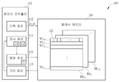
본 발명의 일 실시예에 따른 플래시 메모리 소자를 도시한 다이어그램인 도 1을 참조해 보겠다. 플래시 메모리 소자(flash memory device)(100)는 메모리 컨트롤러(memory controller)(102) 및 플래시 메모리(104)를 포함한다. 메모리 컨트롤러(102)는 플래시 메모리(104)에 결합되고, 플래시 메모리(104)의 컨트롤 액세스(control access)(즉, 기록 및 판독)에 배열된다. 메모리 컨트롤러(102)는 기록 회로(write circuit)(112), 검사 회로(check circuit)(114), 재생 회로(refresh circuit)(116), 및 기타 회로(other circuitry)(118)를 포함하고, 기타 회로(118)는 판독 회로(read circuit), 삭제 회로(erase circuit), ECC 회로(Error Checking and Correcting circuit) 등을 포함할 수 있다. 기록 회로(112)는 플래시 메모리(104)에 결합되고, 입력 데이터 D_IN을 플래시 메모리(104) 내의 저장 공간에 저장하도록 구성되며, 저장 공간은 단일 페이지의 메모리 셀 또는 워드라인(word line) 내에 위치한 메모리 셀 등과 같은 플래시 메모리(104)의 블록의 일부분이다. 검사 회로(114)는 입력 데이터 D_IN이 저장되어 있는 저장 공간의 신뢰도를 검사하도록 구성된다. 재생 회로(116)는 검사 회로(114) 및 플래시 메모리(104)에 결합되고, 저장 공간의 신뢰도가 기설정된 기준을 충족하면 입력 데이터 D_IN에 기초하여 저장 공간을 재생하도록 구성된다. 기록 회로(112), 검사 회로(114) 및 재생 회로(116)의 동작은 이후에 구체적으로 설명한다. 본 발명은 플래시 메모리(104)에 적용되는 재생 방식에 중점을 두고 있으므로, 기타 회로(118)에 포함된 회로 구성요소들에 의해 수행되는 삭제 동작, 판독 동작 및 ECC 디코딩 동작에 관한 상세한 내용은 설명을 간결하게 하기 위해 본 명세서에서는 생략된다. 또한, 기록 회로(112), 검사 회로(114), 재생 회로(116), 및 기타 회로(118)는 특정 소프트웨어 또는 펌웨어 코드를 실행하는 회로로 설계될 수 있으며, 상기 회로 중 적어도 두 개의 회로는 해당 소프트웨어 또는 펌웨어의 제어 하에 서로 다른 동작을 수행하는 동일한 하드웨어를 공유할 수 있다.1, which is a diagram illustrating a flash memory device according to an embodiment of the present invention. A
플래시 메모리(104)에 관하여, 이는 복수개의 블록 BK0, BK1, …, BKM을 포함할 수 있으며, M은 실제 설계 요구사항에 따른 임의의 양의 값일 수 있다. 각각의 블록은 서로 다른 워드라인 WL0, WL1, WL2, …, WLL에 위치하는 복수개의 메모리셀(122)을 포함하며, L은 실제 설계 요구사항에 따른 임의의 양의 값일 수 있다. 예를 들어, L=86 이다. 각각의 워드라인에 위치하는 메모리셀(122)은 K 페이지에 속하며, K는 실제 설계 요구사항에 따른 임의의 양의 값일 수 있다. 예를 들어 K=3 이다.With respect to the
플래시 메모리(104)의 데이터 액세스에 관하여, 설계된 페이지에 포함된 메모리셀(122)로부터 저장된 데이터를 판독하기 위해 플래시 메모리(104)에 대하여 페이지 기반의 판독 동작이 수행될 수 있고, 설계된 페이지에 포함된 메모리셀(122)에 저장된 데이터를 프로그래밍하기 위해 플래시 메모리(104)에 대하여 페이지 기반의 기록 동작이 수행될 수 있으며, 설계된 블록에 포함된 모든 메모리셀(122)에 저장된 데이터를 삭제하기 위해 플래시 메모리(104)에 대하여 블록 기반의 삭제 동작이 수행될 수 있다. 본 실시예에서, 각각의 메모리셀(122)은 N-비트 멀티-레벨 셀일 수 있으며, N은 2를 초과하는 양의 값이다. 예를 들어, 각각의 메모리셀(122)은 3-비트 멀티-레벨 셀(TLC(Triple-Level Cell)로 알려져 있음)일 수 있다.With respect to the data access of the
인접하는 메모리셀의 부동 게이트 간 결합 효과는 문턱 전압 분배의 시프팅(shifting) 및/또는 확장을 야기할 수 있다. 이와 같은 문턱 전압 분배의 시프팅 및/또는 확장은 판독 마진을 악화시키며, 이에 따라 판독 데이터 에러가 발생한다. 인접하는 메모리셀의 부동 게이트 간 결합 효과로부터 발생한 문턱 전압 분배의 시프팅 및/또는 확장을 완화하기 위해서, 기록 회로(112)는 초기 프로그램 동작 및 상기 초기 프로그램 동작에 추종하는 적어도 하나의 리프로그램(reprogram) 동작을 통해 기록 동작을 수행하도록 구성된다.The coupling effect between the floating gates of adjacent memory cells may cause shifting and / or expansion of the threshold voltage distribution. Such shifting and / or expansion of the threshold voltage distribution worsens the read margin, and thus a read data error occurs. In order to mitigate the shifting and / or expansion of the threshold voltage distribution resulting from the coupling effect between the floating gates of adjacent memory cells, the
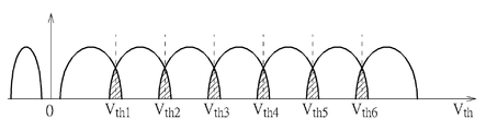
플래시 메모리(104)가 TLC 플래시 메모리일 경우, 각각의 메모리셀(122)은 3비트의 데이터를 저장하기 위한 여덟 가지 상태 중 하나를 가지도록 프로그래밍될 것이다. 기록 회로(112)가 입력 데이터 D_IN을 플래시 메모리(104)의 저장 공간(예를 들어, 블록 BK0의 워드라인 WL0에 있는 메모리셀(122))에 기록하면, 설계된 저장 공간 내에 포함된 각각의 메모리셀(122)을 프로그래밍하기 위해 리프로그램 기반의 방법이 사용된다. 도 2는 제1 프로그램 동작(즉, 초기 프로그램 동작)의 수행 후의 메모리 셀의 문턱 전압 분배를 도시한 다이어그램이다. 각각의 메모리셀(122)에 대하여, 초기 프로그램 동작은 메모리셀(122)을 저장될 3비트 데이터를 기반의 타겟 상태로 프로그래밍되도록 한다. 도 2에 도시된 바와 같이, 서로 다른 상태 상호간을 구별하기 위해 기준 문턱 전압 0 및 VTH1-VTH6이 사용된다. 초기 프로그램 동작이 수행되었더라도, 인접한 메모리 셀의 부동 게이트 간 결합 효과에 의해 교란된 문턱 전압 분배로 인해 서로 다른 상태 상호간을 명확하게 구별하기는 어렵다. 보다 구체적으로, 애매한 데이터값 영역이 존재한다(사선으로 표시됨). 이에 따라 제1 리프로그램 동작이 수행된다. 도 3은 제2 프로그램 동작(즉, 제1 리프로그램 동작)의 수행 후의 메모리 셀의 문턱 전압 분배를 도시한 다이어그램이다. 제1 리프로그램 동작은 초기 프로그램 동작으로부터 발생한 문턱 전압 분배를 개선하기 위해 사용된다. 도 3으로부터 알 수 있듯이, 제2 프로그램 동작(즉, 제1 리프로그램 동작)은 서로 다른 상태에 대한 문턱 전압 분배를 보다 더 분명하게 하기 때문에, 애매한 데이터 영역의 크기가 감소된다. 그러나 애매한 데이터값 영역의 문턱 전압을 갖는 프로그래밍된 메모리셀을 잘못 판독할 가능성은 여전히 존재한다. 따라서, 제2 리프로그램 동작이 수행된다. 도 4는 제3 프로그램 동작(즉, 제2 리프로그램 동작)의 수행 후의 메모리 셀의 문턱 전압 분배를 도시한 다이어그램이다. 도 4으로부터 알 수 있듯이, 제2 리프로그램 동작이 수행되면, 서로 다른 상태에 대한 각각의 문턱 전압 분배는 모두 확실하게 구별될 수 있다.If the
기록 회로(112)에 의해 응용되는 리프로그램 기반의 방법이 문턱 전압 분배를 보다 좁게 만들고 프로그래밍된 메모리셀에 의해 유지된 서로 다른 상태 상호간을 정확하게 구별하도록 추종하는 판독 동작을 가능하게 하기 위해 바람직한 범위 내로 더욱 분명하게 할 수는 있지만, 프로그래밍된 메모리셀(122)의 데이터 유지 장애는 여전히 발생할 수 있다. 데이터 유지 장애가 발생하면, 서로 다른 상태에 대한 문턱 전압 분배가 종(bell) 모양으로 확대되면서 시프트 다운(shift down)될 수 있다. 도 5는 데이터 유지 장애가 발생할 경우의 메모리 셀의 문턱 전압 분배를 도시한 다이어그램이다. 데이터 유지 장애로 인해 문턱 전압 분배가 변경됨에 따라, 초기 기준 문턱 전압을 이용하여 데이터 에러를 판독한 것일 수 있다. 즉, 입력 데이터 D_IN이 저장되어 있는 저장 공간(예를 들어, 블록 BK0의 워드라인 WL0에 있는 메모리셀(122))의 신뢰도가 저하되면, 메모리 컨트롤러(102)는 플래시 메모리(104)의 저장 공간으로부터 저장된 데이터를 정확하게 판독하기 어려울 수 있다. 본 실시예에서, 검사 회로(114)는 입력 데이터가 저장되어 있는 저장 공간의 신뢰도를 검사하고, 재생 회로(116)는 저장 공간의 신뢰도가 기설정된 기준을 충족하면 입력 데이터 D_IN에 기초하여 저장 공간에 대해 재생 동작을 수행한다. 예를 들어, 검사 회로(114)는, 입력 데이터 D_IN이 저장되어 있는 저장 공간에 데이터 유지 장애가 있는지 여부를 감지하고, 데이터 유지 장애의 발생이 감지되면 저장 공간의 신뢰도가 기설정된 기준을 충족했다는 판정을 한다. 한 설계의 실시예에서, 검사 회로(114)는 데이터 유지 장애가 발생하는지 여부를 판정하는 기타 회로(118) 내에 포함된 ECC 회로에 의해 제공된 정보를 지시할 수 있다. 예를 들어, ECC회로가, 디코딩에 실패하거나, 플래시 메모리(104) 내의 저장 공간으로부터 판독된 저장 데이터에 대해 디코딩 동작(예를 들어 하드 디코딩 동작 또는 소프트 디코딩)을 적용할 경우 문턱을 초과하는 다수의 에러 비트를 결정하면, 검사 회로(114)는 저장 공간의 메모리셀(122)에 데이터 유지 장애가 있는 것으로 판정한다. 재생 기반의 데이터 유지 복원은 저장 공간 내에 저장된 데이터를 복원을 가능하게 할 수 있다(예를 들어, 블록 BK0의 워드라인 WL0). 예를 들어, 복수의 판독 동작을 통해 저장된 데이터가 복원되도록 ECC 회로에 의해 복잡한 디코딩 알고리즘(예를 들어, 소프트 디코딩 알고리즘)이 실행된다. The reprogram based method applied by the
일반적으로, TLC 블록은 TLC 블록의 복원된 데이터를 버퍼링하기 위해 세 개의 SLC 블록을 요구할 수 있다. 한 설계의 실시예에서, 메모리 컨트롤러(102)는 TLC 블록 하나의 복원된 데이터를 플래시 메모리 내에 할당된 세 개의 SLC 블록들에 저장할 수 있다. 다른 설계의 실시예에서는, TLC 블록 하나의 복원된 데이터가 메모리 컨트롤러(102)의 내부 버퍼에 저장될 수 있다.In general, a TLC block may require three SLC blocks to buffer the recovered data of a TLC block. In one embodiment of the design, the
저장된 데이터(즉, 입력 데이터 D_IN)가 데이터 유지 장애가 있는 저장 공간으로부터 성공적으로 복원된 후에, 재생 회로(116)는 저장 공간(예를 들어, 블록 BK0의 워드라인 WL0에 있는 메모리셀(122))에 대해 재생 동작을 수행하도록 검사 회로(114)로부터 명령을 받는다. 본 실시예에서, 입력 데이터 D_IN을 플래시 메모리(104)의 저장 공간에 기록하기 위해 기록 회로(112)가 리프로그램 기반의 방법을 이용하므로, 재생 회로(116)에 의해 수행되는 재생 동작은, 저장 공간으로부터 복원된 입력 데이터 D_IN을 저장 공간 내의 본래 저장 위치에 기록하기 위해 저장 공간에 적용되는 부가적인 리프로그램 동작이다. 따라서, 도 54에 도시된 문턱 전압 분배는 재생 회로(116)에 의해 수행되는 부가적인 리프로그램 동작에 의해 개선된다. 도 6은 재생 동작이 수행된 후의 메모리 셀의 문턱 전압 분배를 도시한 다이어그램이다. 바람직한 실시예에서, 재생 회로(116)는, 저장 공간 내의 본래 저장 위치에 위치한 메모리셀(122)을 더 높은 문턱값에 기록하기 위해 저장 공간으로부터 복원된 입력 데이터 D_IN을 지시하도록 구성되고, 이에 따라 노이즈 마진(noise margin)이 좋아지면서 문턱 전압 분배는 정교해진다. 다시 말해, 기록 회로(112)에 의해 저장 공간에 저장된 입력 데이터 D_IN이 제1 초기 설정의 기준 문턱 전압값(즉, 도 4에 도시된 0 및 VTH1-VTH6)에 기초하여 판독되고, 재생 회로(116)에 의해 저장 공간에 저장된 입력 데이터가 제1 초기 설정의 기준 문턱 전압값과는 다른 제2 초기 설정의 기준 문턱 전압값(즉, 도 6에 도시된 0 및 VTH1’-VTH6’)에 기초하여 판독된다. 또한, 제2 초기 설정의 기준 문턱 전압값에서 정해진 가장 높은 기준 문턱 전압값(즉, VTH6’)은, 제1 초기 설정의 기준 문턱 전압값에서 정해진 가장 높은 기준 문턱 전압값(즉, VTH6)보다 크다. Stored data (that is, the input data D_IN) is after the successfully restored from the storage space in the data holding impaired, the
전술한 바와 같이, 제2 초기 설정의 기준 문턱 전압값(즉, 0 및 VTH1’-VTH6’)은 재생 동작이 완료된 후의 제1 초기 설정의 기준 문턱 전압값(즉, 0 및 VTH1-VTH6)과 상이하다. 따라서, 추종하는 판독 동작을 촉진시키기 위해, 재생 회로(116)는 제2 초기 설정의 기준 문턱 전압값을 지시하는 지시자(indicator) IT를 더 저장하도록 구성된다. 이렇게 함으로써, 기타 회로(118)에 포함된 판독 회로는, 재생 회로(116)에 의해 재생된 저장 공간에 대하여 판독 동작을 수행하기 위해 정확한 기준 문턱 전압값 0, VTH1’-VTH6’을 사용하도록 지시자 IT를 지시할 수 있다. 제2 초기 설정의 기준 문턱 전압값을 지시하는 지시자 IT는 메모리 컨트롤러(102)에 있는 대응 테이블에 저장될 수 있다.As described above, the reference threshold voltage values (i.e., 0 and V TH1 '-V TH6 ') of the second initial setting are the reference threshold voltage values of the first initial setting after the completion of the reproducing operation (i.e., 0 and V TH1 - V TH6 ). Thus, to facilitate subsequent read operations, the
동일한 블록의 데이터가 순차적으로 저장될 수 있기 때문에(예를 들어, 짧은 시간 간격 동안의 저장), 본 명세서에 제안된 재생 동작은 블록 기반의 동작일 수 있다. 예를 들어, 블록 내 워드라인 중 하나에 저장된 데이터가 데이터 유지 장애의 영향을 받은 것이 발견되면, 모든 블록은 재생 회로(116)에 의해 재생될 수 있다. 예를 들어, 검사 회로(114)가, 블록 BK0의 워드라인 WL0에 있는 메모리셀(122)에 데이터 유지 장애가 있음을 발견하면, 재생 회로(116)는 동일한 블록 BK0의 모든 워드라인 WL0-WLL을 재생할 수 있다. 바람직하게는, 보다 나은 문턱 전압 분배의 개선을 위해, 블록의 워드라인 재생 순서가 블록의 워드라인에의 데이터 기록 순서를 따른다. 예를 들어, 기록 회로(112)가 리프로그램 방법을 이용하여 블록 BK0의 워드라인 WL0-WLL에 데이터를 순차적으로 기록한 경우, 재생 회로(116)는 블록 BK0의 워드라인 WL0-WLL에 순차적으로 재생 동작을 적용한다.Since the data of the same block can be stored sequentially (e.g., storage during short time intervals), the playback operation proposed herein may be a block-based operation. For example, if the data stored in one of the word lines in the block is found to have been affected by a data retention failure, then all of the blocks may be recovered by the
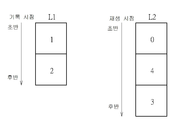
바람직한 실시예에서, 재생 기반의 데이터 유지 복원은 플래시 메모리(104)의 일반적인 데이터 액세서 환경에서 간섭 없이 수행된다. 예를 들어, 검사 회로(114)는, 플래시 메모리 소자(100)가 가동될 때마다 블록들 BK0-BKM 중 적어도 하나에서의 데이터 유지 장애 발생을 감지하도록, 기타 회로(118)에 포함된 판독 회로 및 ECC 회로에 명령을 한다. 검사 회로(114)는 제1 목록(L1) 및 제2 목록(L2)를 유지할 수 있으며, 제1 목록(L1)은, 기록 회로(112)에 의해 기록되었으나 기록 시의 오름차순 또는 기록 시의 내림차순으로 재생 회로(116)에 의해 재생되지는 않은 지표값(index value)를 기록하고, 제2 목록(L2)는, 재생 시의 오름차순 또는 재생 시의 내림차순으로 재생 회로(116)에 의해 재생된 지표값을 기록한다. 도 7은 검사 회로(114)에 의해 기록된 제1 목록(L1) 및 제2 목록(L2)의 예시를 도시한 다이어그램이다. 예시의 제1 목록(L1)은 지표값 ‘3’, ‘1’ 및 ‘2’를 순서대로 기록하며, 이는 기록 회로(112)가 블록 BK1에 데이터를 기록하기 전에 블록 BK3에 데이터를 기록하고, 기록 회로(112)가 블록 BK2에 데이터를 기록하기 전에 블록 BK1에 데이터를 기록함을 의미한다. 예시의 제2 목록(L2)은 지표값 ‘0’ 및 ‘4’를 순서대로 기록하며, 이는 재생 회로(116)가 블록 BK4를 재생하기 전에 블록 BK0을 재생함 의미한다. 제1 목록(L1)의 도움으로, 검사 회로(114)는, 블록 BK3이 가장 이른 기록 시점에 데이터를 저장하였으며 이에 따라 블록 BK1, BK2, BK3 중에서 데이터 유지 장애가 발생할 확률이 가장 높다는 것을 인식한다. 마찬가지로, 제2 목록(L2)의 도움으로, 검사 회로(114)는, 블록 BK0이 가장 이른 재생 시점에 데이터를 저장하였으며 이에 따라 블록 BK0과 BK4 중에서 데이터 유지 장애가 발생할 확률이 가장 높다는 것을 인식한다. 플래시 소자(100)가 가동되면, 검사 회로(114)는, 저장된 데이터(예를 들어, 하나의 워드라인의 데이터)를 블록 BK3으로부터 판독하고 블록 BK3으로부터 판독된 데이터에 대하여 하드 디코딩 동작을 수행하도록, 기타 회로(118)에 포함된 판독 회로 및 ECC 회로에 명령을 한다. 또한, 플래시 소자(100)가 가동되면(또는 다른 어떤 기설정된 시점, 또는 메모리 컨트롤러(102)가 가동되지 않는(idle) 시점), 검사 회로(114)는, 저장된 데이터(예를 들어, 하나의 워드라인의 데이터)를 블록 BK0으로부터 판독하고 블록 BK0으로부터 판독된 데이터에 대하여 하드 디코딩 동작을 수행하도록, 기타 회로(118)에 포함된 판독 회로 및 ECC 회로에 더 명령한다. BK3으로부터 판독된 데이터의 하드 디코딩에 디코딩 오류가 있을 경우, BK3에 대하여 상술한 재생 동작을 수행하도록 BK3가 액티베이팅된다. BK0으부터 판독된 데이터의 하드 디코딩에 디코딩 오류가 있을 경우에는, BK0에 대하여 더 이상 데이터 유지 복원이 적용되지 않는다. 상술한 재생 동작이 BK3에 대하여 수행되면, 이에 상응하여 검사 회로(114)에 의해 제1 목록(L1) 및 제2 목록(L2)이 업데이트된다. 도 8은 검사 회로(114)에 의해 기록된, 업데이트된 제1 목록(L1) 및 업데이트된 제2 목록(L2)의 예시를 도시한 다이어그램이다. 도 8에 도시된 바와 같이, 업데이트된 제1 목록(L1)은 이제 지표값 ‘1’ 및 ‘2’를 순서대로 기록하고, 업데이트된 제2 목록(L2)은 이제 지표값 ‘0’, ‘4’ 및 ‘3’을 순서대로 기록한다. 이에 따라, 플래시 소자(100)가 이후에 가동되면, (블록 BK1 및 BK2 중에서 데이터 유지 장애가 발생할 확률이 가장 높은 것으로 제1 목록(L1)에 의해 지시된) 블록 BK1 및 (블록 BK0, BK4 및 BK3 중에서 데이터 유지 장애가 발생할 확률이 가장 높은 것으로 제2 목록(L2)에 의해 지시된) 블록 BK0에 저장된 데이터가 검사될 것이다.In a preferred embodiment, playback-based data retention is performed without interference in the general data access environment of
(모든 재생된 블록들 중에서 데이터 유지 장애가 발생할 확률이 가장 높은 것으로 제2 목록(L2)에 의해 지시된) 블록 BK0으로부터 판독된 데이터의 하드 디코딩에 디코딩 오류가 있을 경우를 가정해보자. 한 설계의 예시에서, 블록 BK0에 대하여 다시 재생 동작을 수행하도록 재생 회로(116)가 액티베이팅될 수 있다. 다른 설계의 예시에서는, 블록 BK0으로부터 복원된 데이터를 대체 블록에 프로그래밍하고 블록 BK0을 삭제하는 종래의 데이터 유지 복원 방식이 액티베이팅될 수 있다.Assume that there is a decoding error in the hard decoding of the data read from the block BK 0 (indicated by the second list L2) that has the highest probability of occurrence of data retention failure among all the reproduced blocks. In one example of a design, the
데이터 유지 장애가 있는 블록을 삭제하는 종래의 데이터 유지 복원 방식과 비교할 때, 제안된 본 발명의 데이터 유지 복원 방식은 블록을 삭제하는 대신 블록을 재생한다. 이렇게 함으로써, 플래시 메모리(104)의 P/E 순환 횟수가 증가하지 않는다. 또한, 데이터 유지 장애가 있는 블록의 데이터를 다른 블록으로 옮기는 종래의 데이터 유지 복원 방식과 비교할 때, 제안된 본 발명의 데이터 유지 복원 방식은 어떠한 데이터도 옮기지 않고 블록을 재생한다. 따라서, 논리적 어드레스를 물리적 어드레스로 맵핑하는 테이블(logical-to-physical address mapping table)을 업데이트할 필요가 없으며, 논리적 어드레스를 물리적 어드레스로 맵핑하는 테이블은 페이지 모드 또는 블록 모드에서 사용될 수 있다. 보다 구체적으로, 논리적 어드레스를 물리적 어드레스로 맵핑하는 테이블이 페이지 모드에서 사용될 경우, 논리적 어드레스를 물리적 어드레스로 맵핑하는 테이블은 논리적 페이지를 물리적 페이지로 변환하기 위해 인용된다. 논리적 어드레스를 물리적 어드레스로 맵핑하는 테이블이 블록 모드에서 사용될 경우, 논리적 어드레스를 물리적 어드레스로 맵핑하는 테이블은 논리적 블록을 물리적 블록으로 변환하기 위해 인용된다.Compared with the conventional data retention method for erasing a block having a data retention failure, the proposed data retention method of the present invention reproduces a block instead of deleting the block. By doing this, the number of P / E cycles in the
당업자는 본 발명의 요지를 유지하면서 장치 및 방법에 다양한 변경 및 개조가 가해질 수 있음을 쉽게 알 수 있을 것이다. 따라서 상술한 내용은 첨부된 청구범위의 한계 및 경계에 한하여서만 해석되어야 한다. It will be readily apparent to those skilled in the art that various changes and modifications can be made to the apparatus and method while maintaining the gist of the present invention. Accordingly, the foregoing should be interpreted only as being limited to the limits and boundaries of the appended claims.
Claims (20)
상기 플래시 메모리의 블록에 기록되었으나 기록 시의 오름차순 또는 기록 시의 내림차순으로 재생되지 않은 블록의 지표값(index value)을 기록한 제1 목록 및 재생 시의 오름차순 또는 재생 시의 내림차순으로 재생된 블록의 지표값을 기록한 제2 목록을 이용하여, 입력 데이터가 저장되어 있는 상기 저장 공간에 데이터 유지 장애(data-retention disturbance)가 있는지 여부를 감지함으로써, 상기 입력 데이터가 저장되어 있는 상기 저장 공간의 신뢰도를 검사하는 단계; 및
상기 저장 공간의 신뢰도가 기설정된 기준을 충족하면, 상기 입력 데이터에 기초하여 상기 저장 공간에 대해 재생(refresh) 동작을 수행하는 단계
를 포함하는 플래시 메모리의 재생 방법.Performing a write operation to store input data in a storage space in the flash memory;
A first list recorded in a block of the flash memory in which an index value of a block that has not been reproduced in an ascending order of recording or in a descending order of recording is recorded and an index of a block reproduced in descending order of reproduction By checking whether there is a data-retention disturbance in the storage space in which the input data is stored by using the second list in which the input data is stored, thereby checking the reliability of the storage space in which the input data is stored ; And
Performing a refresh operation on the storage space based on the input data if the reliability of the storage space satisfies a predetermined criterion
And reproducing the flash memory.
상기 저장 공간은 복수의 N-비트 멀티-레벨 셀로 구성되고, N은 2를 초과하는 양의 값인,
플래시 메모리의 재생 방법.The method according to claim 1,
Wherein the storage space is comprised of a plurality of N-bit multi-level cells, and wherein N is a positive value greater than two,
A method of reproducing a flash memory.
상기 기록 동작은, 초기 프로그램 동작 및 상기 초기 프로그램 동작에 추종하는 적어도 하나의 리프로그램(reprogram) 동작을 통해 상기 저장 공간에 상기 입력 데이터를 저장하는,
플래시 메모리의 재생 방법.The method according to claim 1,
Wherein the recording operation stores the input data in the storage space through an initial program operation and at least one reprogram operation following the initial program operation,
A method of reproducing a flash memory.
상기 재생 동작은, 상기 저장 공간으로부터 복원된 상기 입력 데이터를 상기 저장 공간 내의 본래 저장 위치로 프로그래밍하기 위해 상기 저장 공간에 적용되는 부가적인 리프로그램 동작인,
플래시 메모리의 재생 방법.5. The method of claim 4,
Wherein the reproducing operation is an additional reprogramming operation applied to the storage space to program the input data recovered from the storage space to an original storage location in the storage space,
A method of reproducing a flash memory.
상기 기록 동작에 의해 상기 저장 공간에 저장된 상기 입력 데이터가, 제1 초기 설정의 기준 문턱 전압값에 기초하여 판독되고,
상기 재생 동작에 의해 상기 저장 공간에 저장된 상기 입력 데이터가, 상기 제1 초기 설정의 기준 문턱 전압값과는 다른 제2 초기 설정의 기준 문턱 전압값에 기초하여 판독되는,
플래시 메모리의 재생 방법.The method according to claim 1,
The input data stored in the storage space by the recording operation is read based on a reference threshold voltage value of a first initial setting,
Wherein the input data stored in the storage space is read out based on a reference threshold voltage value of a second initial setting different from the reference threshold voltage value of the first initial setting by the reproducing operation,
A method of reproducing a flash memory.
상기 제2 초기 설정의 기준 문턱 전압값에서 정해진 가장 높은 기준 문턱 전압값이, 상기 제1 초기 설정의 기준 문턱 전압값에서 정해진 가장 높은 기준 문턱 전압값보다 더 큰,
플래시 메모리의 재생 방법.The method according to claim 6,
Wherein the highest reference threshold voltage value determined at the reference threshold voltage value of the second initial setting is greater than the highest reference threshold voltage value set at the reference threshold voltage value of the first initial setting,
A method of reproducing a flash memory.
상기 저장 공간에 대한 상기 재생 동작의 수행 이후에, 상기 제2 초기 설정의 기준 문턱 전압값을 지시하는 지시자(indicator)를 저장하는 단계를 더 포함하는
플래시 메모리의 재생 방법.The method according to claim 6,
Further comprising the step of storing an indicator indicating a reference threshold voltage value of the second initial setting after performing the reproducing operation on the storage space
A method of reproducing a flash memory.
상기 저장 공간은 상기 플래시 메모리의 블록의 일부분인,
플래시 메모리의 재생 방법.The method according to claim 1,
Wherein the storage space is part of a block of the flash memory,
A method of reproducing a flash memory.
상기 저장 공간의 상기 신뢰도가 상기 기설정된 기준을 충족하면, 상기 플래시 메모리의 상기 블록의 나머지 부분에 대하여 재생 동작을 수행하는 단계를 더 포함하는
플래시 메모리의 재생 방법.10. The method of claim 9,
And if the reliability of the storage space meets the predetermined criterion, performing a reproducing operation on the remaining portion of the block of the flash memory
A method of reproducing a flash memory.
상기 플래시 메모리의 블록에 기록되었으나 기록 시의 오름차순 또는 기록 시의 내림차순으로 재생되지 않은 블록의 지표값(index value)을 기록한 제1 목록 및 재생 시의 오름차순 또는 재생 시의 내림차순으로 재생된 블록의 지표값을 기록한 제2 목록을 이용하여, 입력 데이터가 저장되어 있는 상기 저장 공간에 데이터 유지 장애가 있는지 여부를 감지함으로써, 상기 입력 데이터가 저장되어 있는 상기 저장 공간의 신뢰도를 검사하도록 구성된 검사 회로; 및
상기 검사 회로 및 상기 플래시 메모리에 결합되고, 상기 저장 공간의 상기 신뢰도가 기설정된 기준을 충족하면 상기 입력 데이터에 기초하여 상기 저장 공간을 재생하도록 구성된 재생 회로
를 포함하는 플래시 메모리의 메모리 컨트롤러.A write circuit coupled to the flash memory and configured to store input data in a storage space in the flash memory;
A first list recorded in a block of the flash memory in which an index value of a block that has not been reproduced in an ascending order of recording or in a descending order of recording is recorded and an index of a block reproduced in descending order of reproduction An inspection circuit configured to detect a reliability of the storage space in which the input data is stored by detecting whether or not there is a data maintenance failure in the storage space in which the input data is stored using the second list in which the value is recorded; And
A playback circuit coupled to the test circuit and the flash memory and configured to play back the storage space based on the input data if the reliability of the storage space meets a predetermined criterion,
Wherein the flash memory is a flash memory.
상기 메모리 컨트롤러에 의해 액세스된 상기 저장 공간은 복수의 N-비트 멀티-레벨 셀로 구성되고, N은 2를 초과하는 양의 값인,
플래시 메모리의 메모리 컨트롤러.12. The method of claim 11,
Wherein the storage space accessed by the memory controller is comprised of a plurality of N-bit multi-level cells, and wherein N is a positive value greater than two,
Memory controller in flash memory.
상기 기록 회로가, 초기 프로그램 동작 및 상기 초기 프로그램 동작에 추종하는 적어도 하나의 리프로그램(reprogram) 동작을 통해 상기 저장 공간에 상기 입력 데이터를 저장하는,
플래시 메모리의 메모리 컨트롤러.12. The method of claim 11,
Wherein the recording circuit stores the input data in the storage space through at least one reprogram operation following the initial program operation and the initial program operation,
Memory controller in flash memory.
상기 재생 회로가, 상기 저장 공간으로부터 복원된 상기 입력 데이터를 상기 저장 공간 내의 본래 저장 위치로 프로그래밍하기 위해 상기 저장 공간에 대하여 부가적인 리프로그램 동작을 수행하는,
플래시 메모리의 메모리 컨트롤러.15. The method of claim 14,
Wherein the playback circuit performs an additional reprogramming operation on the storage space to program the input data recovered from the storage space to an original storage location in the storage space.
Memory controller in flash memory.
상기 기록 회로에 의해 상기 저장 공간에 저장된 상기 입력 데이터가, 제1 초기 설정의 기준 문턱 전압값에 기초하여 판독되고,
상기 재생 회로에 의해, 상기 저장 공간에 저장된 상기 입력 데이터가, 상기 제1 초기 설정의 기준 문턱 전압값과는 다른 제2 초기 설정의 기준 문턱 전압값에 기초하여 판독되는,
플래시 메모리의 메모리 컨트롤러.12. The method of claim 11,
The input data stored in the storage space by the recording circuit is read based on a reference threshold voltage value of a first initial setting,
Wherein the reproducing circuit reads the input data stored in the storage space based on a reference voltage value of a second initial setting different from the reference voltage value of the first initial setting,
Memory controller in flash memory.
상기 제2 초기 설정의 기준 문턱 전압값에서 정해진 가장 높은 기준 문턱 전압값이, 상기 제1 초기 설정의 기준 문턱 전압값에서 정해진 가장 높은 기준 문턱 전압값보다 더 큰,
플래시 메모리의 메모리 컨트롤러.17. The method of claim 16,
Wherein the highest reference threshold voltage value determined at the reference threshold voltage value of the second initial setting is greater than the highest reference threshold voltage value set at the reference threshold voltage value of the first initial setting,
Memory controller in flash memory.
상기 저장 공간을 재생한 후에 상기 재생 회로가 제2 초기 설정의 기준 문턱 전압값을 지시하는 지시자(indicator)를 저장하는,
플래시 메모리의 메모리 컨트롤러.17. The method of claim 16,
Wherein the reproducing circuit stores an indicator indicating a reference threshold voltage value of a second initial setting after reproducing the storage space,
Memory controller in flash memory.
상기 메모리 컨트롤러에 의해 액세스된 상기 저장 공간은 상기 플래시 메모리의 블록의 일부분인,
플래시 메모리의 메모리 컨트롤러.12. The method of claim 11,
Wherein the storage space accessed by the memory controller is part of a block of the flash memory,
Memory controller in flash memory.
상기 재생 회로는, 상기 저장 공간의 상기 신뢰도가 상기 기설정된 기준을 충족하면, 상기 플래시 메모리의 상기 블록의 나머지 부분을 재생하도록 더 구성되는,
플래시 메모리의 메모리 컨트롤러.20. The method of claim 19,
Wherein the playback circuit is further configured to play the remaining portion of the block of the flash memory if the reliability of the storage space meets the predetermined criteria,
Memory controller in flash memory.
Applications Claiming Priority (2)
| Application Number | Priority Date | Filing Date | Title |
|---|---|---|---|
| US13/967,371 | 2013-08-15 | ||
| US13/967,371 US9627085B2 (en) | 2012-11-29 | 2013-08-15 | Refresh method for flash memory and related memory controller thereof |
Publications (2)
| Publication Number | Publication Date |
|---|---|
| KR20150020023A KR20150020023A (en) | 2015-02-25 |
| KR101653293B1 true KR101653293B1 (en) | 2016-09-01 |
Family
ID=52579581
Family Applications (1)
| Application Number | Title | Priority Date | Filing Date |
|---|---|---|---|
| KR1020140041013A Active KR101653293B1 (en) | 2013-08-15 | 2014-04-07 | Refresh method for flash memory and related memory controller thereof |
Country Status (1)
| Country | Link |
|---|---|
| KR (1) | KR101653293B1 (en) |
Citations (4)
| Publication number | Priority date | Publication date | Assignee | Title |
|---|---|---|---|---|
| JP2007035242A (en) | 2005-06-24 | 2007-02-08 | Micronics Internatl Co Ltd | Flash memory refresh method |
| US20090161466A1 (en) | 2007-12-20 | 2009-06-25 | Spansion Llc | Extending flash memory data retension via rewrite refresh |
| KR101136273B1 (en) | 2007-07-19 | 2012-04-19 | 마이크론 테크놀로지, 인크. | Refresh of non-volatile memory cells based on fatigue conditions |
| US20120203951A1 (en) | 2010-01-27 | 2012-08-09 | Fusion-Io, Inc. | Apparatus, system, and method for determining a configuration parameter for solid-state storage media |
-
2014
- 2014-04-07 KR KR1020140041013A patent/KR101653293B1/en active Active
Patent Citations (4)
| Publication number | Priority date | Publication date | Assignee | Title |
|---|---|---|---|---|
| JP2007035242A (en) | 2005-06-24 | 2007-02-08 | Micronics Internatl Co Ltd | Flash memory refresh method |
| KR101136273B1 (en) | 2007-07-19 | 2012-04-19 | 마이크론 테크놀로지, 인크. | Refresh of non-volatile memory cells based on fatigue conditions |
| US20090161466A1 (en) | 2007-12-20 | 2009-06-25 | Spansion Llc | Extending flash memory data retension via rewrite refresh |
| US20120203951A1 (en) | 2010-01-27 | 2012-08-09 | Fusion-Io, Inc. | Apparatus, system, and method for determining a configuration parameter for solid-state storage media |
Also Published As
| Publication number | Publication date |
|---|---|
| KR20150020023A (en) | 2015-02-25 |
Similar Documents
| Publication | Publication Date | Title |
|---|---|---|
| US9627085B2 (en) | Refresh method for flash memory and related memory controller thereof | |
| US9229644B2 (en) | Targeted copy of data relocation | |
| JP5130646B2 (en) | Storage device | |
| KR101392701B1 (en) | Embedded mapping information for memory devices | |
| KR101405741B1 (en) | Stripe-based non-volatile multilevel memory operation | |
| US8910002B2 (en) | NAND flash-based storage device with built-in test-ahead for failure anticipation | |
| US10613943B2 (en) | Method and system for improving open block data reliability | |
| US9189313B2 (en) | Memory system having NAND-type flash memory and memory controller with shift read controller and threshold voltage comparison module | |
| US10592134B1 (en) | Open block stability scanning | |
| JP2019168937A (en) | Memory system, control method and controller | |
| KR20140020364A (en) | Embedded mapping information for memory devices | |
| KR101468432B1 (en) | Flash memory refresh techniques triggered by controlled scrub data reads | |
| US20110047322A1 (en) | Methods, systems and devices for increasing data retention on solid-state mass storage devices | |
| JP2013522776A (en) | Multi-level cell self-RAID flash data protection | |
| KR20080066959A (en) | Modified data storage and handling methods | |
| US10867633B1 (en) | Reduced adjacent track erasure from write retry | |
| JP2012517068A (en) | Memory device, memory management device, and memory management method | |
| US10628247B2 (en) | Flash memory testing according to error type pattern | |
| US11550710B2 (en) | Data processing method and memory controller utilizing the same | |
| US10528348B2 (en) | Data management method for storage media | |
| JP2014194817A (en) | Storage device | |
| KR101653293B1 (en) | Refresh method for flash memory and related memory controller thereof | |
| US8885406B2 (en) | Memory device, memory control device, and memory control method | |
| KR101604949B1 (en) | Method and apparatus for controlling memory | |
| JP5264459B2 (en) | Semiconductor memory device |
Legal Events
| Date | Code | Title | Description |
|---|---|---|---|
| A201 | Request for examination | ||
| PA0109 | Patent application |
St.27 status event code: A-0-1-A10-A12-nap-PA0109 |
|
| PA0201 | Request for examination |
St.27 status event code: A-1-2-D10-D11-exm-PA0201 |
|
| D13-X000 | Search requested |
St.27 status event code: A-1-2-D10-D13-srh-X000 |
|
| D14-X000 | Search report completed |
St.27 status event code: A-1-2-D10-D14-srh-X000 |
|
| PG1501 | Laying open of application |
St.27 status event code: A-1-1-Q10-Q12-nap-PG1501 |
|
| E902 | Notification of reason for refusal | ||
| PE0902 | Notice of grounds for rejection |
St.27 status event code: A-1-2-D10-D21-exm-PE0902 |
|
| E902 | Notification of reason for refusal | ||
| PE0902 | Notice of grounds for rejection |
St.27 status event code: A-1-2-D10-D21-exm-PE0902 |
|
| E13-X000 | Pre-grant limitation requested |
St.27 status event code: A-2-3-E10-E13-lim-X000 |
|
| P11-X000 | Amendment of application requested |
St.27 status event code: A-2-2-P10-P11-nap-X000 |
|
| P13-X000 | Application amended |
St.27 status event code: A-2-2-P10-P13-nap-X000 |
|
| E701 | Decision to grant or registration of patent right | ||
| PE0701 | Decision of registration |
St.27 status event code: A-1-2-D10-D22-exm-PE0701 |
|
| GRNT | Written decision to grant | ||
| PR0701 | Registration of establishment |
St.27 status event code: A-2-4-F10-F11-exm-PR0701 |
|
| PR1002 | Payment of registration fee |
St.27 status event code: A-2-2-U10-U11-oth-PR1002 Fee payment year number: 1 |
|
| PG1601 | Publication of registration |
St.27 status event code: A-4-4-Q10-Q13-nap-PG1601 |
|
| FPAY | Annual fee payment |
Payment date: 20190620 Year of fee payment: 4 |
|
| PR1001 | Payment of annual fee |
St.27 status event code: A-4-4-U10-U11-oth-PR1001 Fee payment year number: 4 |
|
| PR1001 | Payment of annual fee |
St.27 status event code: A-4-4-U10-U11-oth-PR1001 Fee payment year number: 5 |
|
| PR1001 | Payment of annual fee |
St.27 status event code: A-4-4-U10-U11-oth-PR1001 Fee payment year number: 6 |
|
| PR1001 | Payment of annual fee |
St.27 status event code: A-4-4-U10-U11-oth-PR1001 Fee payment year number: 7 |
|
| PR1001 | Payment of annual fee |
St.27 status event code: A-4-4-U10-U11-oth-PR1001 Fee payment year number: 8 |
|
| PR1001 | Payment of annual fee |
St.27 status event code: A-4-4-U10-U11-oth-PR1001 Fee payment year number: 9 |
|
| PR1001 | Payment of annual fee |
St.27 status event code: A-4-4-U10-U11-oth-PR1001 Fee payment year number: 10 |
|
| U11 | Full renewal or maintenance fee paid |
Free format text: ST27 STATUS EVENT CODE: A-4-4-U10-U11-OTH-PR1001 (AS PROVIDED BY THE NATIONAL OFFICE) Year of fee payment: 10 |