KR101616787B1 - Magnetic shielding sheet and method for manufacturing the same - Google Patents
Magnetic shielding sheet and method for manufacturing the same Download PDFInfo
- Publication number
- KR101616787B1 KR101616787B1 KR1020150095251A KR20150095251A KR101616787B1 KR 101616787 B1 KR101616787 B1 KR 101616787B1 KR 1020150095251 A KR1020150095251 A KR 1020150095251A KR 20150095251 A KR20150095251 A KR 20150095251A KR 101616787 B1 KR101616787 B1 KR 101616787B1
- Authority
- KR
- South Korea
- Prior art keywords
- electromagnetic wave
- sheet
- wave absorbing
- permeability
- magnetic
- Prior art date
- Legal status (The legal status is an assumption and is not a legal conclusion. Google has not performed a legal analysis and makes no representation as to the accuracy of the status listed.)
- Expired - Fee Related
Links
Images




Classifications
-
- H—ELECTRICITY
- H05—ELECTRIC TECHNIQUES NOT OTHERWISE PROVIDED FOR
- H05K—PRINTED CIRCUITS; CASINGS OR CONSTRUCTIONAL DETAILS OF ELECTRIC APPARATUS; MANUFACTURE OF ASSEMBLAGES OF ELECTRICAL COMPONENTS
- H05K9/00—Screening of apparatus or components against electric or magnetic fields
- H05K9/0073—Shielding materials
- H05K9/0075—Magnetic shielding materials
-
- B—PERFORMING OPERATIONS; TRANSPORTING
- B32—LAYERED PRODUCTS
- B32B—LAYERED PRODUCTS, i.e. PRODUCTS BUILT-UP OF STRATA OF FLAT OR NON-FLAT, e.g. CELLULAR OR HONEYCOMB, FORM
- B32B7/00—Layered products characterised by the relation between layers; Layered products characterised by the relative orientation of features between layers, or by the relative values of a measurable parameter between layers, i.e. products comprising layers having different physical, chemical or physicochemical properties; Layered products characterised by the interconnection of layers
- B32B7/04—Interconnection of layers
- B32B7/12—Interconnection of layers using interposed adhesives or interposed materials with bonding properties
-
- H—ELECTRICITY
- H05—ELECTRIC TECHNIQUES NOT OTHERWISE PROVIDED FOR
- H05K—PRINTED CIRCUITS; CASINGS OR CONSTRUCTIONAL DETAILS OF ELECTRIC APPARATUS; MANUFACTURE OF ASSEMBLAGES OF ELECTRICAL COMPONENTS
- H05K9/00—Screening of apparatus or components against electric or magnetic fields
- H05K9/0073—Shielding materials
- H05K9/0081—Electromagnetic shielding materials, e.g. EMI, RFI shielding
- H05K9/0088—Electromagnetic shielding materials, e.g. EMI, RFI shielding comprising a plurality of shielding layers; combining different shielding material structure
Landscapes
- Engineering & Computer Science (AREA)
- Microelectronics & Electronic Packaging (AREA)
- Physics & Mathematics (AREA)
- Electromagnetism (AREA)
- Shielding Devices Or Components To Electric Or Magnetic Fields (AREA)
Abstract
본 발명의 일 실시예는 자기장 차폐 시트 및 그의 제조방법에 관한 것으로, 해결하고자 하는 기술적 과제는 100 kHz 내지 300kHz의 전자파 노이즈 주파수 대역에서 전자파 흡수율이 우수하게 하는데 있다.
이를 위해 본 발명의 일 실시예는 브레이킹처리된 다수 개의 비정질 조각 편이 구비되는 전자파 흡수 시트; 상기 전자파 흡수 시트의 일면 상에 접착된 보호 필름; 및 상기 일면의 반대면인 전자파 흡수 시트의 타면 상에 접착된 접착 필름을 포함하고, 주파수가 100 kHz 내지 300kHz인 상태에서 Q(quality factor)값이 80이상인 자기장 차폐 시트를 개시한다.An embodiment of the present invention relates to a magnetic shield sheet and a method of manufacturing the same, and a technical problem to be solved is to make the electromagnetic wave absorption rate excellent in an electromagnetic noise frequency band of 100 kHz to 300 kHz.
To this end, an embodiment of the present invention is an electromagnetic wave absorbing sheet comprising a plurality of braked amorphous piece pieces; A protective film adhered on one surface of the electromagnetic wave absorbing sheet; And an adhesive film adhered on the other surface of the electromagnetic wave absorbing sheet which is the opposite surface of the one surface, and has a quality factor value Q of 80 or more with a frequency of 100 kHz to 300 kHz.
Description
본 발명의 일 실시예는 전자파 흡수 효과가 큰 자기장 차폐 시트 및 그의 제조방법에 관한 것이다.
An embodiment of the present invention relates to a magnetic shield sheet having a large electromagnetic wave absorbing effect and a method of manufacturing the same.
핸드폰에 근거리 통신, 근거리 카드 결제기능을 탑재하기 위한 것이다. 이러한 기능을 가지는 3장의 필름을 합쳐서 핸드폰 케이스에 내장시킨 결과, 원하는 특성이 나오지 않았다.It is intended to equip mobile phones with local communication and local card payment functions. As a result of incorporating the three films having these functions into the cellular phone case, the desired characteristics were not obtained.
그런데, 아몰퍼스 시트를 넣었더니 원하는 특성이 나온다.However, when the amorphous sheet is inserted, the desired characteristics are obtained.
투자율을 높이기 위하여 아몰퍼스 시트를 롤러로 가압하여 잘게 부수는 작업을 한다. 롤러로 가압하기 전에 양면 테이프의 양쪽에 아몰퍼스 시트를 각각 부착시키고, 아몰퍼스 외면에 보호필름을 부착시킨 후 롤러로 가압하여서 브레이킹하여, 결과적으로 300kHz에서 50 이상의 허수부 투자율을 얻을 수 있었다.In order to increase the permeability, the amorphous sheet is pressed by a roller to be crushed. The amorphous sheets were respectively attached to both sides of the double-sided tape before being pressed by the rollers, and a protective film was attached to the outer surface of the amorphous body, followed by pressurizing with a roller to braking and consequently obtaining an imaginary part permeability of 50 or more at 300 kHz.
최근 디지털 전자기기와 관련하여 전자 장치의 회로 신호처리 속도의 고속화, 고기능화, 소형화 그리고 제품 형태의 박형화에 대한 요구가 더욱 가속화되고 있다. 인쇄회로기판(PCB)에 실장되는 각종 반도체 소자들의 데이터 처리속도가 고속화되고 있어서, 인쇄회로기판(PCB)에 실장되는 능동소자와 수동소자의 부품 장착밀도도 높아져 가고 있다.In recent years, there has been a growing demand for higher speed, higher performance, miniaturization and thinning of product form of circuit signal processing speed of electronic devices in relation to digital electronic devices. The data processing speed of various semiconductor devices mounted on a printed circuit board (PCB) is increased, and the mounting density of the active device and the passive device mounted on the printed circuit board (PCB) is also increasing.
이와 같은 소자들은 고속신호에 의해 전압, 전류의 급격한 변화를 동반하기 때문에 유도성 노이즈를 발생시켜 고주파 노이즈의 발생원이 되고 있다. 이들 능동소자 및 수동소자 같은 부품들은 인쇄 배선들 인쇄 회로 상에서 매우 가깝게 위치하고 있어서 소형 디지털 전자기기 내부 소자들 간 또는 소자와 배선간의 전자 결합에 의한 누화(cross talk) 문제를 일으키거나, 기기 밖으로 전자파를 방사시켜 다른 기기에 영향을 주는 EMI(Electro Magnetic Interference: 전자파 장해 또는 전자파 간섭) 문제를 일으킬 수 있다.Such devices are accompanied by rapid changes in voltage and current due to high-speed signals, and thus induce inductive noise, which is a source of high frequency noise. Components such as active and passive components are located very close to the print wiring circuitry, causing cross talk problems between internal components of small digital electronic devices or between components and wiring, EMI (Electro Magnetic Interference) that affects other devices may be caused.
또한, 전자기기에서 발생되는 전자파가 인체에 장기 노출될 경우 녹내장, 생식능력의 저하 등의 인체에 영향을 미치게 된다.In addition, when electromagnetic waves generated from electronic devices are exposed to the human body for a long period of time, they affect the human body such as glaucoma and deterioration of reproductive ability.
상기 EMI에 대한 대책으로 제안되는 전자파 차폐(Electro Magnetic Shielding)는 전자 기기 내부에서 발생하는 전자파 노이즈를 케이스 밖으로 방사시키지 않고 또한 외부에서 침입하는 전자파 노이즈를 흡수하거나 차단하는 것을 말한다.Electro Magnetic Shielding (EMI), which is proposed as a countermeasure against the above-mentioned EMI, refers to absorbing or interrupting the electromagnetic noise generated from the outside without radiating the electromagnetic noise generated inside the electronic device out of the case.
기기 내부에 공간적 여유가 있는 디지털 전자기기의 경우에는 유도성 노이즈를 발생시키는 회로에 필터를 접속하여 노이즈를 제거하거나 회로간의 거리를 멀리 떨어뜨리거나, 전자파 차폐재로 실드(shield)하여 그라운딩(grounding)을 하는 등의 EMI 대책이 취해지고 있다.In the case of a digital electronic device having a space inside the device, a filter may be connected to a circuit for generating inductive noise to remove noise or to reduce the distance between the circuits, shielding with an electromagnetic shielding material, And EMI measures are taken.
그러나, 소형 디지털 전자기기들의 경우 인쇄회로기판(PCB) 위에 전자부품이 고밀도로 장착되어 있어서 앞에서 언급한 필터 등에 의한 노이즈 대책 방법으로는 실장 공간이 필요할 뿐만 아니라 소형화, 박형화를 위해 설계단계에서부터의 고려가 필요하기 때문에, 제품수명이 짧은 제품에 대한 시급한 노이즈 대책으로는 적합하지 않다.However, in the case of small-sized digital electronic devices, electronic components are mounted on a printed circuit board (PCB) at a high density. As a countermeasure against noise caused by the above-mentioned filter and the like, not only a mounting space is required but also consideration from the design stage It is not suitable as an urgent noise countermeasure for a product having a short product life.
이러한 이유로 인해 최근에는 소형 디지털 전자기기의 회로기판에서 주요 노이즈원이 되는 능동 부품들에 의해 발생하는 유도성 전자파 노이즈를 억제하기 위해 입/출력단에 약 0.2mm 이상의 비교적 두꺼운 연자성 복합 자성체 시트(sheet)가 사용되고 있다.For this reason, in recent years, in order to suppress inductive electromagnetic noise generated by active components, which are major noise sources in a circuit board of a small digital electronic device, a relatively thick soft magnetic compound sheet ) Are used.
이 같은 복합 자성체 시트 재료의 투자율은 실수부 투자율과 허수부 투자율 성분으로 구성되며, 노이즈의 억제 효율은 억제하고자 하는 전자파 노이즈 주파수 대역에서 허수부 투자율이 클수록, 또한 복합자성체의 두께가 두꺼울수록 억제 효과가 크다.The magnetic permeability of the composite magnetic sheet material is composed of the real magnetic permeability and the imaginary magnetic permeability. The suppression efficiency of the noise is suppressed as the imaginary magnetic permeability is increased in the electromagnetic noise frequency band to be suppressed, .
한편, 디지털 전자기기의 크기가 더욱 소형화되는 추세이기 때문에 이 같은 복합 자성체의 두께가 더욱 얇으면서도 전자파의 억제 효과가 우수한 제품이 요망되고 있다. 또한, 전자기기의 소형화 추세에 따라 전술한 준 마이크로파 대역에 사용하는 노이즈 대책용 복합 자성체 시트의 박형화가 요구되고 있다.On the other hand, since the size of a digital electronic device is becoming smaller, a product having such a thin composite magnetic body and excellent electromagnetic wave suppression effect is desired. In addition, with the trend toward miniaturization of electronic devices, it is required to reduce the thickness of composite magnetic sheet for noise countermeasures used in the above-mentioned sub-microwave band.
복합 자성체 시트의 경우 자성 손실에 의한 노이즈 감소효과를 이용하는 것으로 박형화하기 위하여는 허수부 투자율이 더 커져야 한다. 현재의 자성 재료는 약 10 ~ 100 MHz 보다 낮은 주파수 대역 또는 그 보다 높은 주파수 대역에서, 얇은 두께와 전도 노이즈 억제효과를 동시에 만족시키지 못한다는 문제점이 있다.
In the composite magnetic sheet, the imaginary part permeability must be larger in order to reduce the noise by the magnetic loss. The present magnetic material has a problem that it can not simultaneously satisfy the thin thickness and the conduction noise suppressing effect in a frequency band lower than about 10 to 100 MHz or higher.
본 발명의 일 실시예는 100 kHz 내지 300kHz의 전자파 노이즈 주파수 대역에서 전자파 흡수율이 우수한 자기장 차폐 시트 및 그의 제조방법을 제공한다.
An embodiment of the present invention provides a magnetic shield sheet having an excellent electromagnetic wave absorption rate in an electromagnetic noise frequency band of 100 kHz to 300 kHz and a method of manufacturing the same.
본 발명의 일 실시예에 의한 자기장 차폐 시트는 브레이킹처리된 다수 개의 비정질 조각 편이 구비되는 전자파 흡수 시트; 상기 전자파 흡수 시트의 일면 상에 접착된 보호 필름; 및 상기 일면의 반대면인 전자파 흡수 시트의 타면 상에 접착된 접착 필름을 포함하고, 주파수가 100 kHz 내지 300kHz인 상태에서 Q(quality factor)값이 80이상일 수 있다.The electromagnetic shielding sheet according to an embodiment of the present invention includes: an electromagnetic wave absorbing sheet having a plurality of braked amorphous pieces; A protective film adhered on one surface of the electromagnetic wave absorbing sheet; And an adhesive film adhered on the other surface of the electromagnetic wave absorbing sheet which is the opposite surface of the one surface, and the quality factor value may be 80 or more at a frequency of 100 kHz to 300 kHz.
상기 Q값은 수학식 1에 의하여 산출될 수 있다..The Q value can be calculated by Equation (1).
[수학식 1][Equation 1]

여기서, k는 상수이며, u′는 제1 투자율이고, u″는 제2 투자율임.Here, k is a constant, u 'is a first permeability, and u " is a second permeability.
상기 제1 투자율은 상기 전자파 흡수 시트의 실수 투자율이다.The first magnetic permeability is a real permeability of the electromagnetic wave absorbing sheet.
상기 제2 투자율은 상기 전자파 흡수 시트의 허수 투자율이다.And the second magnetic permeability is an imaginary magnetic permeability of the electromagnetic wave absorbing sheet.
상기 브레이킹 처리되지 않은 상태에서의 Q값은 10 내지 50일 수 있다.The Q value in the unbraked state may be 10 to 50. [
상기 비정질 조각 편은 다수의 비정질 리본을 포함하되, 상기 비정질 리본은 Fe계 비정질 합금, Co계 비정질 합금 또는 나노 결정립 합금으로 이루어질 수 있다.The amorphous piece may include a plurality of amorphous ribbons, and the amorphous ribbon may be composed of an Fe-based amorphous alloy, a Co-based amorphous alloy, or a nanocrystalline alloy.
상기 적어도 하나 이상으로 구비된 전자파 흡수 시트 사이에는 접착층이 구비될 수 있다.An adhesive layer may be provided between the electromagnetic wave absorbing sheets provided at least one.
또한, 본 발명의 다른 실시예에 따른 전자파 흡수 시트의 제조 방법은 적어도 하나 이상의 전자파 흡수 시트를 공급하는 제1 단계; 상기 전자파 흡수 시트를 300℃ 내지 600℃에서 30분 내지 4시간동안 열처리하는 제2 단계; 상기 전자파 흡수 시트 사이에 접착 필름을 부착하는 제3 단계; 상기 접착 필름이 부착된 면에 대하여 반대인 전자파 흡수 시트의 일면에 보호 필름을 부착하여 자기장 차폐 시트를 형성하는 제4 단계; 상기 자기장 차폐 시트를 브레이킹 처리하는 제5 단계; 및 상기 브레이킹 처리된 자기장 차폐 시트를 라미네이팅하는 제6 단계;를 포함하고, 상기 라미네이팅된 자기장 차폐 시트는 주파수가 100 kHz 내지 300kHz인 상태에서 Q(quality factor)값이 80이상일 수 있다.According to another aspect of the present invention, there is provided a method of manufacturing an electromagnetic wave absorbing sheet, including: a first step of supplying at least one electromagnetic wave absorbing sheet; A second step of heat-treating the electromagnetic wave-absorbing sheet at 300 ° C to 600 ° C for 30 minutes to 4 hours; A third step of attaching an adhesive film between the electromagnetic wave absorbing sheets; A fourth step of attaching a protective film to one surface of the electromagnetic wave absorbing sheet opposite to the surface to which the adhesive film is attached to form a magnetic shielding sheet; A fifth step of braking the magnetic shielding sheet; And laminating the braked magnetic shielding sheet. The laminating magnetic shielding sheet may have a quality factor (Q) of 80 or more at a frequency of 100 kHz to 300 kHz.
상기 라미네이팅된 자기장 차폐 시트를 소정의 크기로 커팅하는 제7 단계를 더 포함할 수 있다.
And a seventh step of cutting the laminated magnetic shielding sheet to a predetermined size.
본 발명의 일 실시예에 따른 자기장 차폐 시트 및 그의 제조방법은 비정질 리본을 브레이킹 처리하여 100 kHz 내지 300kHz의 전자파 노이즈 주파수 대역에서 품질계수가 높도록 하고 있기 때문에, 전자파 흡수율이 우수한 자기장 차폐 시트를 제공할 수 있다.The magnetic shield sheet according to an embodiment of the present invention and the method of manufacturing the same provide a magnetic shield sheet having an excellent electromagnetic wave absorption rate because the amorphous ribbon is subjected to a braking treatment to increase the quality factor in the electromagnetic noise frequency band of 100 kHz to 300 kHz can do.
또한, 본 발명의 일 실시예는 박막이고 제조공정이 간단하기 때문에, 생산성 향상과 제조비용 감소효과를 구현할 수 있다.
In addition, since the embodiment of the present invention is a thin film and the manufacturing process is simple, it is possible to realize an improvement in productivity and a reduction in manufacturing cost.
도 1은 본 발명의 일 실시예에 따른 자기장 차폐 시트를 나타내는 단면도이다.
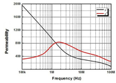
도 2는 본 발명의 일 실시예에 따른 자기장 차폐 시트에서 주파수에 따른 제1 투자율 및 제2 투자율의 변화를 나타내는 그래프이다.
도 3a 및 3b는 본 발명의 일 실시예에 따른 자기장 차폐 시트에서 브레이킹 처리의 유무의 상태에서 주파수에 따른 제1 투자율 및 제2 투자율의 변화를 나타내는 그래프이다.
도 4는 본 발명의 다른 실시예에 따른 자기장 차폐 시트의 제조 방법을 나타내는 순서도이다.1 is a cross-sectional view illustrating a magnetic shield sheet according to an embodiment of the present invention.
FIG. 2 is a graph showing changes in the first magnetic permeability and the second magnetic permeability according to frequency in the magnetic shield sheet according to an embodiment of the present invention. FIG.
3A and 3B are graphs showing changes in the first magnetic permeability and the second magnetic permeability according to the frequency in the presence or absence of the braking process in the magnetic shield sheet according to the embodiment of the present invention.
4 is a flowchart showing a method of manufacturing a magnetic shield sheet according to another embodiment of the present invention.
본 명세서에서 사용되는 용어에 대해 간략히 설명하고, 본 발명에 대해 구체적으로 설명하기로 한다.The terms used in this specification will be briefly described and the present invention will be described in detail.
본 발명에서 사용되는 용어는 본 발명에서의 기능을 고려하면서 가능한 현재 널리 사용되는 일반적인 용어들을 선택하였으나, 이는 당 분야에 종사하는 기술자의 의도 또는 판례, 새로운 기술의 출현 등에 따라 달라질 수 있다. 또한, 특정한 경우는 출원인이 임의로 선정한 용어도 있으며, 이 경우 해당되는 발명의 설명 부분에서 상세히 그 의미를 기재할 것이다. 따라서 본 발명에서 사용되는 용어는 단순한 용어의 명칭이 아닌, 그 용어가 가지는 의미와 본 발명의 전반에 걸친 내용을 토대로 정의되어야 한다.While the present invention has been described in connection with what is presently considered to be the most practical and preferred embodiment, it is to be understood that the invention is not limited to the disclosed embodiments. Also, in certain cases, there may be a term selected arbitrarily by the applicant, in which case the meaning thereof will be described in detail in the description of the corresponding invention. Therefore, the term used in the present invention should be defined based on the meaning of the term, not on the name of a simple term, but on the entire contents of the present invention.
명세서 전체에서 어떤 부분이 어떤 구성요소를 "포함"한다고 할 때, 이는 특별히 반대되는 기재가 없는 한 다른 구성요소를 제외하는 것이 아니라 다른 구성요소를 더 포함할 수 있음을 의미한다. When an element is referred to as "including" an element throughout the specification, it is to be understood that the element may include other elements as well, without departing from the spirit or scope of the present invention.
아래에서는 첨부한 도면을 참고하여 본 발명의 실시예에 대하여 본 발명이 속하는 기술 분야에서 통상의 지식을 가진 자가 용이하게 실시할 수 있도록 상세히 설명한다. 그러나 본 발명은 여러 가지 상이한 형태로 구현될 수 있으며 여기에서 설명하는 실시예에 한정되지 않는다. 그리고 도면에서 본 발명을 명확하게 설명하기 위해서 설명과 관계없는 부분은 생략하였으며, 명세서 전체를 통하여 유사한 부분에 대해서는 유사한 도면 부호를 붙였다.
Hereinafter, embodiments of the present invention will be described in detail with reference to the accompanying drawings so that those skilled in the art can easily carry out the present invention. The present invention may, however, be embodied in many different forms and should not be construed as limited to the embodiments set forth herein. In order to clearly illustrate the present invention, parts not related to the description are omitted, and similar parts are denoted by like reference characters throughout the specification.
도 1은 본 발명의 일 실시예에 따른 자기장 차폐 시트를 나타내는 단면도이고, 도 2는 본 발명의 일 실시예에 따른 자기장 차폐 시트에서 주파수에 따른 제1 투자율 및 제2 투자율의 변화를 나타내는 그래프이며, 도 3a 및 3b는 본 발명의 일 실시예에 따른 자기장 차폐 시트에서 브레이킹 처리의 유무 상태에서 주파수에 따른 제1 투자율 및 제2 투자율의 변화를 나타내는 그래프이다.FIG. 1 is a cross-sectional view illustrating a magnetic shield sheet according to an embodiment of the present invention. FIG. 2 is a graph illustrating changes in a first magnetic permeability and a second magnetic permeability according to frequency in a magnetic shield sheet according to an embodiment of the present invention 3A and 3B are graphs showing changes in the first magnetic permeability and the second magnetic permeability according to the frequency in the presence or absence of the braking process in the magnetic shield sheet according to the embodiment of the present invention.
도 1을 참고하면, 본 발명의 일 실시예에 따른 자기장 차폐 시트(100)는 전자파 흡수 시트(120), 보호 필름(110), 접착 필름(130) 및 릴리즈 필름(140)을 포함한다.Referring to FIG. 1, a
일반적으로, 자기장 차폐 시트는 대표적으로 스마트 폰의 무선충전, NFC(근거리 무선통신), MST(마그네틱 보안전송)등을 포함하여 광범위하게 전자기기의 적용하여 활용될 수 있다. 여기서, 무선충전은 세가지 방법으로 구분되는데 전자기 유도 방식, 자기 공명 방식, 전자기파 방식으로 구분된다. 현재 상용화된 무선충전 기술은 대부분 전자기 유도 방식을 사용하는데, 이 전자기 유도 방식은 전력 송신부인 1차 코일에서 자기장을 발생시키면 이 자기장이 수신부의 2차 코일에 유도되어 전류를 공급하는 전자기유도를 이용한 기술이다. 이러한 무선충전 기술로서의 전자기 유도 방식은 'QI 표준이라 불리는 WPC(Wireless Power Consortium)와 PMA(Power Matters Alliance)를 중심으로 표준제정이 이루어지고 있다. WPC는 100~205kHz의 전력 주파수 대역을 사용하고, PMA는277~357kHz 또는 118~153kHz 대역을 사용한다. 또한, 근거리 무선통신(Near Field Communication, NFC)은 RFID(radio frequency identification) 기술 중 하나로서, 13.56MHz의 주파수 대역을 사용하는 비접촉식 근거리 무선 통신 기술이고, 가까운 거리의 데이터를 전송하는 기술로 교통, 티켓, 지불 등 여러 서비스에서 사용되고 있다. 또한, 마그네틱 보안 전송(Magnetic Secure Transmission, MST)은 마그네틱 신용카드를 긁으면 자기장이 발생하면서 카드 정보가 단말기로 전달되는데 이 원리에서 힌트를 얻어 스마트폰을 카드 단말기에 대면 자기장이 나오도록 설계된 기술이다. 이와 같이, 자기장 차폐 시트가 활용될 수 있는 무선충전, NFC(근거리 무선통신), MST(마그네틱 보안전송) 등은 각 기능 별로 공진 주파수는 다르지만, 실제로 자기장 차폐시트는 일정 주파수에서 한정되지 않고 넓은 영역 주파수에서도 전자파 차폐 기능을 가질 수 있다. 다만, 본 발명에서는 대중화된 WPC에 PMA까지 적용될 수 있는 자기장 차폐 시트에 적용하기 위한 주력 주파수인 100~300kHz의 주파수 전용으로 높은 Q값의 성능을 가지는 자기장 차폐 시트를 제공할 수 있다.In general, the magnetic shielding sheet can be widely applied to electronic appliances including wireless charging of a smart phone, NFC (short-range wireless communication), MST (magnetic security transmission), and the like. Here, wireless charging can be classified into three methods: electromagnetic induction method, magnetic resonance method, and electromagnetic wave method. Most of the commercially available wireless charging technologies use electromagnetic induction. In this electromagnetic induction method, when a magnetic field is generated in a primary coil, which is a power transmitter, electromagnetic induction in which the magnetic field is induced in a secondary coil Technology. The electromagnetic induction method as the wireless charging technology has been standardized around the WPC (Wireless Power Consortium) and the PMA (Power Matters Alliance) called QI standard. WPC uses the power frequency band of 100 ~ 205kHz, and PMA uses 277 ~ 357kHz or 118 ~ 153kHz band. In addition, Near Field Communication (NFC) is one of radio frequency identification (RFID) technologies, and is a non-contact type short range wireless communication technology using a frequency band of 13.56 MHz. Tickets, and payments. In addition, Magnetic Secure Transmission (MST) is a technology designed to generate a magnetic field when a magnetic credit card is scratched, and card information is transmitted to a terminal. In this way, although the resonance frequencies are different for each function of wireless charging, NFC (short range wireless communication), MST (magnetic security transmission), etc. in which the magnetic shield sheet can be utilized, the magnetic shield sheet is not limited at a certain frequency, It can also have electromagnetic wave shielding function in frequency. However, according to the present invention, it is possible to provide a magnetic shield sheet having a high Q-value performance for a frequency of 100 to 300 kHz, which is a main frequency for application to a magnetic shielding sheet applicable to PMA in popularized WPC.
상기 전자파 흡수 시트(120)는 비정질 합금 또는 나노 결정립 합금으로 이루어진 박판의 리본으로서, 비정질 합금 또는 나노 결정립 합금의 리본을 열처리한 후 브레이킹 처리하여 분리된 다수의 비정질 조각 편으로 이루어져 있다. The electromagnetic wave-absorbing
상기 전자파 흡수 시트(120)는 비정질 합금 또는 나노결정립 합금의 리본을 열처리한 후 브레이킹 처리하여 다수의 비정질 조각편으로 분리된다. 이러한 전자파 흡수 시트(120)의 두께는 10 내지 25㎛로 설정되고, 사용 주파수 대역은 100 kHz 내지 300kHz이다. 이때, 상기 전자파 흡수 시트(120)의 두께가 25㎛를 초과하는 경우, 박막화 추세를 지향하는 휴대 단말기 등에는 적용이 불가능하다. 이러한 전자파 흡수 시트(120)의 두께는 적용되는 비정질 레이어가 증가함에 따라 변경될 수 있다.The electromagnetic wave-absorbing
또한, 상기 비정질 합금은 Fe계 또는 Co계 비정질 합금을 사용할 수 있다.The amorphous alloy may be an Fe-based or a Co-based amorphous alloy.
상기 Fe계 비정질 합금으로는 Fe-Si-B 합금, 필요에 따라 Fe-Si-B-Co 합금을 사용할 수 있고, Co계 비정질 합금으로는 Co-Fe-Ni-Si-B 또는 Co-Fe-Cr-Si-B 합금을 사용할 수 있다.The Fe-Si-B alloy or the Fe-Si-B-Co alloy may be used as the Fe-based amorphous alloy, and the Co-Fe-Ni-Si- Cr-Si-B alloy can be used.
상기 Fe-Si-B 합금은, Fe가 70-90 atomic%, Si 및 B의 합이 10-30 atomic%일 수 있다. Fe를 비롯한 금속의 함유량이 높을수록 포화 자속 밀도가 높아지지만 Fe 원소의 함유량이 과다할 경우 비정질을 형성하기 어려우므로, 본 발명에서는 Fe의 함량이 70-90atomic%인 것이 바람직하다. 또한, Si 및 B의 합이 10-30atomic%의 범위일 때 합금의 비정질 형성능이 가장 우수하다. 이러한 기본 조성에 부식을 방지시키기 위해 Cr, Co 등 내부식성 원소를 20 atomic% 이내로 첨가할 수도 있고, 다른 특성을 부여하도록 필요에 따라 다른 금속 원소를 소량 포함할 수 있다.The Fe-Si-B alloy may have 70-90 atomic% of Fe and 10-30 atomic% of the sum of Si and B in the Fe-Si-B alloy. The higher the content of Fe and other metals, the higher the saturation magnetic flux density. However, when the content of Fe element is excessive, it is difficult to form amorphous. Therefore, in the present invention, the content of Fe is preferably 70-90 atomic%. When the sum of Si and B is in the range of 10-30 atomic%, the amorphous formability of the alloy is the most excellent. In order to prevent corrosion in such a basic composition, corrosion resistance elements such as Cr and Co may be added in an amount of 20 atomic% or less, and a small amount of other metal elements may be added as needed to impart different properties.
상기 나노 결정립 합금은, Fe-Si-B-Cu-Nb 합금을 사용할 수 있으며, 이 경우, Fe가 73-80 at%, Si 및 B의 합이 15-26 at%, Cu와 Nb의 합이 1-5 at%인 것이 바람직하다. 이러한 조성 범위가 리본 형태로 제작된 비정질 합금이 후술하는 열처리에 의해 나노상의 결정립으로 쉽게 석출될 수 있다.The nanocrystalline alloy may be Fe-Si-B-Cu-Nb alloy. In this case, the total amount of Fe is 73-80 at%, the sum of Si and B is 15-26 at%, the sum of Cu and Nb is 1-5 at%. An amorphous alloy having such a composition range in the form of a ribbon can be easily precipitated into nano-phase grains by a heat treatment to be described later.
상기 보호 필름(110)은 전자파 흡수 시트(120)의 상부에 접착되는 필름으로서, 1 내지 75㎛ 두께의 폴리에틸렌 테레프탈레이트(PET) 필름, 폴리이미드 필름, 폴리에스테르 필름, 폴리에틸렌나프탈레이트, 폴리페닐린설페이드(PPS) 필름, 폴리프로필렌(PP) 필름, 폴리테레프탈레이트(PTFE)와 같은 불소 수지계 필름 등의 수지 필름을 사용할 수 있다. 도시되어 있지는 않지만, 상기 보호 필름(110)은 소정의 접착층을 통하여 전자파 흡수 시트(120)의 상부에 접착될 수 있다.The
상기 접착 필름(130)은 전자파 흡수 시트(120)의 하부에 접착되는 접착된 필름으로서, PET(Polyethylene Terephthalate) 필름이 이용될 수 있다. 이러한 접착 필름(130)은 기재의 양측면에 접착층이 형성된다. 상기 접착 필름(130)은 기재가 있는 타입과, 기재가 없이 접착층만으로 형성되는 무기재 타입도 적용이 가능하다. 상기 접착층은 아크릴계 접착제를 사용할 수 있으며, 다른 종류의 접착제를 사용하는 것도 물론 가능하다.The
상기 릴리즈 필름(140)은 접착 필름(130)의 하부에 부착되는 필름으로서, 접착 필름(130)의 제조시에 일체로 형성되며, 전자파 흡수 시트(120)를 전자기기에 부착할 때 박리되어 제거된다.The
상기와 같은 구조를 가지는 자기장 차폐 시트의 전자파 흡수시트(120)는 복수 개의 층으로 구성될 수 있고, 이때 1개의 층당 10 내지 25㎛의 두께를 가질 수 있다. 이때, 상기 전자파 흡수시트(120)의 열처리 후의 핸들링 공정을 고려하면 전자파 흡수시트(120)의 두께는 20 내지 25㎛로 설정될 수 있다. 리본의 두께가 얇을수록 열처리 후 핸들링시에 약간의 충격에도 리본의 깨짐 현상이 발생할 수 있다.The electromagnetic-wave-absorbing
또한, 상기 비정질 리본의 다수의 비정질 조각편은 수십㎛ ~ 3mm 이하의 크기를 가질 수 있다.In addition, a plurality of amorphous pieces of the amorphous ribbon may have a size of several tens of micrometers to 3 mm or less.
또한, 상기 보호 필름(110)은 1-75㎛ 범위일 수 있고, 접착 필름(130)은 10, 20, 30㎛의 두께를 가질 수 있다.Also, the
그러나, 본 발명은 다수의 비정질 조각편의 크기와, 보호 필름(110) 및 접착 필름(130)의 두께를 한정하는 것은 아니다.However, the present invention does not limit the size of the plurality of amorphous pieces and the thickness of the
상기와 같은 공정을 거쳐 제조된 본 자기장 차폐 시트(100)는 주파수가 100 kHz 내지 300kHz인 대역에서 품질 계수값인 Q값이 향상되어 전자파 흡수율이 우수한 특성을 가지게 된다. 여기서, 상기 품질 계수값인 Q값이 높을수록 전자파 흡수 효과가 크게 된다.The
한편, 상기 Q값(quality factor)은 아래 수학식 1에 의하여 산출된다.On the other hand, the quality factor is calculated by the following equation (1).
여기서, k는 상수이며, u′는 제1 투자율이고, u″는 제2 투자율이며, μ는 투자율이다. Here, k is a constant, u 'is a first permeability, u' is a second permeability, and μ is a permeability.
상기 투자율(permeability)은 어떤 물질에 대한 자속이 통과되는 지 여부를 정량화한 계수로서, 복소 투자율을 가지고, 그 복소 투자율은 실수 투자율과 허수 투자율로 구성된다.The permeability is a coefficient that quantifies whether a magnetic flux for a certain material is passed. The permeability has a complex permeability, and the complex permeability is composed of a real permeability and an imaginary permeability.
이때, 상기 제1 투자율은 라미네이팅된 전자파 흡수 시트(120)의 실수 투자율에 해당되고, 제2 투자율은 라미네이팅된 전자파 흡수 시트(120)의 허수 투자율에 해당된다.At this time, the first permeability corresponds to the real permeability of the laminated electromagnetic
상기 실수 투자율은 자기적 성질을 나타내는 성분이고, 허수 투자율은 손실을 나타내는 성분이다.The real permeability is a component representing a magnetic property, and the imaginary permeability is a component representing a loss.
따라서, 수학식 1에 따르면, u′이 높을수록 Q값은 상승하며, u″가 높을수록 Q값은 하락하게 된다.Therefore, according to Equation (1), the higher the value of u ', the higher the value of Q, and the higher the value of u', the lower the value of Q.
이를 기초로, 본 발명에 따른 자기장 차폐 시트(100)는 도 2에 도시된 바와 같이 주파수가 100 kHz 내지 300kHz인 상태에서 Q(quality factor)값이 80이상인 것으로 나타나 매우 우수한 전자파 특성을 가지는 것을 알 수 있다.2, the
또한, 본 발명에 따른 자기장 차폐 시트(100)는, 표 1에 나타난 바와 같이, 브레이킹 공정의 유무에 따른 Q값에 있어 현저한 차이를 보임을 알 수 있다.As shown in Table 1, the
특히, 본 발명에 따른 자기장 차폐 시트(100)는 전자파 흡수 시트(120)가 적어도 1장 이상 적층된 경우를 의미한다. 이와 같이, 본 발명에 따른 자기장 차폐 시트(100)는 1장 이상 적층되고, 1장 이상 적층되는 경우에, Q값이 현저하게 높게 나타남을 알 수 있다.In particular, the
즉, 도 3a에 도시된 바와 같이 브레이킹 처리되지 않은 전자파 흡수 시트(120)는 주파수가 100 kHz 내지 300kHz인 상태에서 Q값이 10 내지 50임을 나타내고 있으나, 도 3b에 도시된 바와 같이 브레이킹 처리된 전자파 흡수 시트(120)는 Q값이 80이상임을 나타내는 것을 알 수 있다.That is, as shown in FIG. 3A, the electromagnetic wave-
한편, 상기 자기장 차폐 시트(100)는 전자파 흡수 시트가 1 장일 경우 전자파 흡수 시트 하부에 접착 필름이 부착되어 총 15 내지 30um의 두께를 가지고, 전자파 흡수 시트가 2 장일 경우 각 전자파 흡수 시트 사이에 접착 필름이 부착되어 총 25 내지 55um의 두께를 가지면, 전자파 흡수 시트가 3 장일 경우 상부 전자파 흡수 시트와 중간 전자파 흡수 시트간, 그리고 중간 전자파 흡수 시트와 하부 전자파 흡수 시트 간에 각각 접착 필름이 부착되어 총 40 내지 85um의 두께를 가지게 된다. 이와 동일한 원리로, 전자파 흡수 시트가 7 장일 경우 자기장 차폐 시트는 총 100 내지 205um의 두께를 가지게 된다.On the other hand, in the case of one electromagnetic wave absorbing sheet, the
이에 따라, 본 발명의 일 실시예에 따른 자기장 차폐시트(100)는 전자파 흡수 시트의 개수에 따라 그 두께가 변경될 수 있으나, Q값과의 관계를 기초하면 15 내지 400um의 두께를 가지는 것이 바람직하다.Accordingly, the thickness of the
결과적으로, 본 발명의 일 실시예에 따른 자기장 차폐 시트(100)는 비정질 리본을 브레이킹 처리하여 100 kHz 내지 300kHz의 전자파 노이즈 주파수 대역에서 품질계수가 높도록 하고 있기 때문에, 전자파 흡수율이 우수한 자기장 차폐 시트(100)를 제공할 수 있다.
As a result, since the
도 4는 본 발명의 다른 실시예에 따른 자기장 차폐 시트의 제조 방법을 나타내는 순서도이다. 4 is a flowchart showing a method of manufacturing a magnetic shield sheet according to another embodiment of the present invention.
도 4를 참조하여 본 발명의 다른 실시예에 따른 자기장 차폐 시트의 제조 방법은, 적어도 하나 이상의 전자파 흡수 시트(120)를 공급하는 제1 단계(S10), 전자파 흡수 시트(120)를 300℃ 내지 600℃에서 30분 내지 4시간동안 열처리하는 제2 단계(S20), 전자파 흡수 시트(120) 사이에 접착 필름(130)을 부착하는 제3 단계(S30), 접착 필름(130)이 부착된 면에 대하여 반대인 전자파 흡수 시트(120)의 일면에 보호 필름(110)을 부착하는 제4 단계(S40), 접착 필름(130)과 보호 필름(110)이 부착된 전자파 흡수 시트(120)를 브레이킹 처리하는 제5 단계(S50), 브레이킹 처리된 전자파 흡수 시트(120)를 라미네이팅하는 제6 단계(S60) 및 라미네이팅된 전자파 흡수 시트(120)를 소정의 크기로 커팅하는 제7 단계(S70)를 포함한다.Referring to FIG. 4, a method of manufacturing a magnetic shield sheet according to another embodiment of the present invention includes a first step (S10) of supplying at least one electromagnetic
보다 구체적으로 설명하자면, 우선 상기 제1 단계(S10)는 비정질 합금 또는 나노결정립 합금으로 이루어진 비정질 리본을 멜트 스피닝에 의한 급냉응고법(RSP)으로 제조한 전자파 흡수 시트(120)를 공급한다.More specifically, in the first step (S10), an amorphous ribbon made of an amorphous alloy or a nano-crystal alloy is supplied to the electromagnetic
상기 제2 단계(S20)는 전자파 흡수 시트(120)가 원하는 투자율을 얻을 수 있도록 300℃ 내지 600℃에서 30분 내지 4시간동안 열처리한다. 이때, 열처리 분위기는 비정질 리본 또는 나노결정립 합금에 포함된 Fe 함량에 따라 분위기 로나 대기 중 혹은 산화 분위기 또는 질소 분위기에서 열처리가 이루어질 수 있다. 또한, 열처리 온도가 300℃ 미만인 경우 자성시트 제조 시 발생한 내부 응력의 풀림(stress relief)이 완벽하게 이루어지지 않아 투자율 등의 자기특성의 불균일이 해소되지 않기 때문에 열처리 시간을 길게 해야 하는 문제가 있고, 600℃를 초과하는 경우 과열처리에 의해 자성시트 내부에 결정화가 급격하게 이루어지고 이에 따라 투자율이 현저하게 낮아져서 원하는 투자율을 나타내지 못하는 문제가 있다. 일반적으로 열처리 온도가 낮으면 처리시간이 길게 소요되고 반대로 열처리 온도가 높으면 처리시간은 단축되는 경향을 나타낸다. 이와 같이, 상기 전자파 흡수 시트(120)에 열처리가 이루어지면 취성이 강하게 되어 후속 공정에서 브레이킹 처리를 실시할 때 쉽게 브레이킹이 이루어질 수 있게 된다.In the second step S20, the electromagnetic wave-absorbing
상기 제3 단계(S30) 및 제4 단계(S40)는, 열처리가 이루어진 전자파 흡수시트를 1장 또는 2 내지 4층의 다층으로 사용하여, 일측에 전자파 흡수 시트(120) 사이에 접착 필름(130)을 부착하고, 접착 필름(130)이 부착된 면에 대하여 반대인 전자파 흡수 시트(120)의 일면에 보호 필름(110)을 부착하여 자기장 차폐 시트(100)를 형성한다. 이때, 접착 필름(130) 상에 릴리즈 필름(140)이 부착될 수 있다.In the third step S30 and the fourth step S40, the heat-treated electromagnetic wave absorbing sheet is used as one or two to four layers of multilayer, and an
그런 다음, 상기 제5 단계(S50)는 자기장 차폐 시트(100)를 브레이킹 처리한다.Then, in the fifth step S50, the
상기 브레이킹 처리는 예를 들어, 보호 필름(110), 전자파 흡수시트, 접착 필름(130) 및 릴리즈 필름(140)이 순차적으로 적층된 자기장 차폐 시트(100)를 금속 롤러와 고무 롤러로 이루어지는 브레이킹 장치(미도시)를 통과시켜서 비정질 리본을 다수의 조각편으로 분리시킨다. 이때, 분리된 다수의 조각편은 양측면에 접착된 접착층에 의해 분리된 상태를 유지하게 된다. 또한, 상기 브레이킹 처리에 의하여 분리된 다수의 조각편은 대략 수십㎛ ~ 3mm 범위의 크기를 갖도록 형성되므로 반자장을 증가시켜서 히스테리시스 로스를 제거함에 따라 시트에 대한 투자율의 균일성을 높일 수 있게 된다.The braking process is performed by, for example, disposing a
상기 제6 단계(S60)는 브레이킹 처리된 자기장 차폐 시트(100)는 조각편 사이의 틈새에 접착제를 채움과 동시에 평탄화, 슬림화 및 안정화를 위한 라미네이트 공정을 실시한다. 이때, 상기 라미네이트 공정을 위한 라미네이트 장치(미도시)는 두 개의 가압롤러 또는 가압부재로 이루어진 롤 프레스 타입 또는 유압 프레스 타입이 사용될 수 있다. 이때, 상기 접착제는 상온에서 가압하면 변형이 가능한 접착제가 사용되거나, 열을 가하면 변형되는 열가소성 접착제가 사용될 수 있다.In the sixth step S60, the
본 발명에서의 브레이킹 장치와 라미네이트 장치는 브레이킹 처리나 라미네이팅 처리가 이루어질 수 있는 장비라면 어떤 장치라도 적용될 수 있다.The braking device and the laminating device according to the present invention can be applied to any device that can perform the braking process or the laminating process.
끝으로, 상기 제7 단계(S70)는 라미네이팅된 자기장 차폐 시트(100)를 제조자가 원하는 길이로 일정하게 컷팅하게 된다. 이에 따라, 본 발명은 라미네이팅된 자기장 차폐 시트(100)를 공정 후반부에 컷팅하고 있기 때문에, 대면적 및 대용량의 자기장 차폐 시트를 제조할 수 있고, 나아가 공정 효율을 향상시킬 수 있다.
Finally, in the seventh step S70, the laminated
상기와 같이 구성된 본 발명의 일 실시예에 따른 자기장 차폐 시트 및 그의 제조방법은 비정질 리본을 브레이킹 처리하여 100 kHz 내지 300kHz의 전자파 노이즈 주파수 대역에서 품질계수가 높도록 하고 있기 때문에, 전자파 흡수율이 우수한 자기장 차폐 시트를 제공할 수 있다. 또한, 본 발명의 일 실시예는 박막이고 제조공정이 간단하기 때문에, 생산성 향상과 제조비용 감소효과를 구현할 수 있다.
Since the magnetic shield sheet and the method of manufacturing the same according to the embodiment of the present invention have a high quality factor in an electromagnetic noise frequency band of 100 kHz to 300 kHz by braking the amorphous ribbon, A shielding sheet can be provided. In addition, since the embodiment of the present invention is a thin film and the manufacturing process is simple, it is possible to realize an improvement in productivity and a reduction in manufacturing cost.
이상에서 설명한 것은 본 발명에 의한 자기장 차폐 시트 및 그의 제조방법을 실시하기 위한 하나의 실시예에 불과한 것으로서, 본 발명은 상기 실시예에 한정되지 않고, 이하의 특허청구범위에서 청구하는 바와 같이 본 발명의 요지를 벗어남이 없이 당해 발명이 속하는 분야에서 통상의 지식을 가진 자라면 누구든지 다양한 변경 실시가 가능한 범위까지 본 발명의 기술적 정신이 있다고 할 것이다.
As described above, the present invention is not limited to the above-described embodiments, and it is to be understood that the present invention is not limited to the above- It will be understood by those of ordinary skill in the art that various changes in form and details may be made therein without departing from the spirit and scope of the present invention.
100: 자기장 차폐 시트 110: 보호 필름
120: 전자파 흡수 시트 130: 접착 필름
140: 릴리즈 필름100: magnetic field shielding sheet 110: protective film
120: electromagnetic wave absorbing sheet 130: adhesive film
140: release film
Claims (13)
상기 전자파 흡수 시트의 일면 상에 접착된 보호 필름; 및
상기 일면의 반대면인 전자파 흡수 시트의 타면 상에 접착된 접착 필름을 포함하는 자기장 차폐 시트에 있어서,
상기 비정질 리본은 Fe-Si-B 합금으로서, Fe가 70 내지 90 at%, Si 및 B의 합이 10 내지 30 at%이며,
상기 자기장 차폐 시트의 두께는 25 내지 55㎛이며,
상기 자기장 차폐 시트는 주파수가 100 kHz인 상태에서 하기 수학식 1에 의하여 산출되는 Q(quality factor)값이 80 이상이고,
상기 브레이킹처리전 Q 값은 10 내지 50인 것을 특징으로 하는 자기장 차폐 시트.
[수학식 1]

여기서, k는 상수이며, μ'는 상기 전자파 흡수 시트의 실수 투자율인 제1 투자율이고, μ"는 상기 전자파 흡수 시트의 허수 투자율인 제2 투자율임.
Two electromagnetic wave absorbing sheets provided with a plurality of braked amorphous ribbons; And
A protective film adhered on one surface of the electromagnetic wave absorbing sheet; And
Shielding sheet comprising an adhesive film adhered on the other surface of the electromagnetic wave absorbing sheet which is the opposite surface of the one surface,
Wherein the amorphous ribbon is an Fe-Si-B alloy having 70 to 90 at% of Fe, 10 to 30 at% of Si and B,
The thickness of the magnetic shielding sheet is 25 to 55 탆,
Wherein the magnetic shield sheet has a quality factor (Q) calculated by the following formula (1) at a frequency of 100 kHz of 80 or more,
Wherein the Q value before the braking treatment is in the range of 10 to 50.
[Equation 1]
Here, k is a constant, μ 'is a first permeability, which is the real permeability of the electromagnetic wave absorbing sheet, and μ "is a second permeability, which is an imaginary permeability of the electromagnetic wave absorbing sheet.
상기 전자파 흡수 시트를 300℃ 내지 600℃에서 30분 내지 4시간동안 열처리하는 제2 단계;
상기 전자파 흡수 시트 사이에 접착 필름을 부착하는 제3 단계;
상기 접착 필름이 부착된 면에 대하여 반대인 전자파 흡수 시트의 일면에 보호 필름을 부착하여 자기장 차폐 시트를 형성하는 제4 단계;
상기 자기장 차폐 시트를 브레이킹 처리하는 제5 단계; 및
상기 브레이킹 처리된 자기장 차폐 시트를 라미네이팅하는 제6 단계;를 포함하고,
상기 비정질 리본은 Fe-Si-B 합금으로서, Fe가 70 내지 90 at%, Si 및 B의 합이 10 내지 30 at%이며,
상기 자기장 차폐 시트의 두께는 25 내지 55㎛이며,
상기 라미네이팅된 자기장 차폐 시트는 주파수가 100 kHz 내지 300kHz인 상태에서 Q(quality factor)값이 80 이상이고,
상기 브레이킹처리전 Q 값은 10 내지 50인 것을 특징으로 하는 자기장 차폐 시트의 제조 방법.
[수학식 1]

여기서, k는 상수이며, μ'는 상기 전자파 흡수 시트의 실수 투자율인 제1 투자율이고, μ"는 상기 전자파 흡수 시트의 허수 투자율인 제2 투자율임.
A first step of supplying two electromagnetic wave absorbing sheets having a plurality of braking processed amorphous ribbons;
A second step of heat-treating the electromagnetic wave-absorbing sheet at 300 ° C to 600 ° C for 30 minutes to 4 hours;
A third step of attaching an adhesive film between the electromagnetic wave absorbing sheets;
A fourth step of attaching a protective film to one surface of the electromagnetic wave absorbing sheet opposite to the surface to which the adhesive film is attached to form a magnetic shielding sheet;
A fifth step of braking the magnetic shielding sheet; And
And a sixth step of laminating the braked magnetic shielding sheet,
Wherein the amorphous ribbon is an Fe-Si-B alloy having 70 to 90 at% of Fe, 10 to 30 at% of Si and B,
The thickness of the magnetic shielding sheet is 25 to 55 탆,
The laminated magnetic shield sheet has a quality factor value of 80 or more at a frequency of 100 kHz to 300 kHz,
Wherein the Q value before the braking treatment is in the range of 10 to 50.
[Equation 1]
Here, k is a constant, μ 'is a first permeability, which is the real permeability of the electromagnetic wave absorbing sheet, and μ "is a second permeability, which is an imaginary permeability of the electromagnetic wave absorbing sheet.
상기 라미네이팅된 자기장 차폐 시트를 소정의 크기로 커팅하는 제7 단계를 더 포함하는 것을 특징으로 하는 자기장 차폐 시트의 제조 방법.
The method of claim 8,
Further comprising a seventh step of cutting the laminated magnetic shielding sheet to a predetermined size.
Priority Applications (1)
| Application Number | Priority Date | Filing Date | Title |
|---|---|---|---|
| KR1020150095251A KR101616787B1 (en) | 2015-07-03 | 2015-07-03 | Magnetic shielding sheet and method for manufacturing the same |
Applications Claiming Priority (1)
| Application Number | Priority Date | Filing Date | Title |
|---|---|---|---|
| KR1020150095251A KR101616787B1 (en) | 2015-07-03 | 2015-07-03 | Magnetic shielding sheet and method for manufacturing the same |
Publications (1)
| Publication Number | Publication Date |
|---|---|
| KR101616787B1 true KR101616787B1 (en) | 2016-04-29 |
Family
ID=55915966
Family Applications (1)
| Application Number | Title | Priority Date | Filing Date |
|---|---|---|---|
| KR1020150095251A Expired - Fee Related KR101616787B1 (en) | 2015-07-03 | 2015-07-03 | Magnetic shielding sheet and method for manufacturing the same |
Country Status (1)
| Country | Link |
|---|---|
| KR (1) | KR101616787B1 (en) |
Cited By (1)
| Publication number | Priority date | Publication date | Assignee | Title |
|---|---|---|---|---|
| WO2019124936A1 (en) * | 2017-12-21 | 2019-06-27 | 주식회사 두산 | Electromagnetic wave absorption film and electromagnetic wave absorption type composite substrate comprising same |
Citations (6)
| Publication number | Priority date | Publication date | Assignee | Title |
|---|---|---|---|---|
| JPH06140783A (en) * | 1992-10-22 | 1994-05-20 | Fujita Corp | Amorphous magnetic shield plate and magnetic shield technique |
| KR20030022890A (en) | 2001-06-21 | 2003-03-17 | 데이진 가부시키가이샤 | Near infrared ray shielding film |
| JP2011171612A (en) * | 2010-02-22 | 2011-09-01 | Alps Electric Co Ltd | Fe-BASED SOFT MAGNETIC ALLOY POWDER AND METHOD OF PRODUCING THE SAME, AND MAGNETIC SHEET FOR VHF BAND AND MOLDED ARTICLE USING THE Fe-BASED SOFT MAGNETIC ALLOY POWDER, AND MAGNETIC CORE FOR VHF BAND |
| KR20120102082A (en) | 2009-12-18 | 2012-09-17 | 도판 인사츠 가부시키가이샤 | Antireflection film |
| KR20130000743A (en) * | 2011-06-24 | 2013-01-03 | 이은정 | Method for making microwave shielding sheet using amorphous metal and microwave shielding sheet using the same |
| KR101399021B1 (en) * | 2012-02-03 | 2014-05-27 | 주식회사 아모센스 | Magnetic Shielding Sheet for Digitizer, Manufacturing Method thereof, and Portable Terminal Equipment Using the Same |
-
2015
- 2015-07-03 KR KR1020150095251A patent/KR101616787B1/en not_active Expired - Fee Related
Patent Citations (6)
| Publication number | Priority date | Publication date | Assignee | Title |
|---|---|---|---|---|
| JPH06140783A (en) * | 1992-10-22 | 1994-05-20 | Fujita Corp | Amorphous magnetic shield plate and magnetic shield technique |
| KR20030022890A (en) | 2001-06-21 | 2003-03-17 | 데이진 가부시키가이샤 | Near infrared ray shielding film |
| KR20120102082A (en) | 2009-12-18 | 2012-09-17 | 도판 인사츠 가부시키가이샤 | Antireflection film |
| JP2011171612A (en) * | 2010-02-22 | 2011-09-01 | Alps Electric Co Ltd | Fe-BASED SOFT MAGNETIC ALLOY POWDER AND METHOD OF PRODUCING THE SAME, AND MAGNETIC SHEET FOR VHF BAND AND MOLDED ARTICLE USING THE Fe-BASED SOFT MAGNETIC ALLOY POWDER, AND MAGNETIC CORE FOR VHF BAND |
| KR20130000743A (en) * | 2011-06-24 | 2013-01-03 | 이은정 | Method for making microwave shielding sheet using amorphous metal and microwave shielding sheet using the same |
| KR101399021B1 (en) * | 2012-02-03 | 2014-05-27 | 주식회사 아모센스 | Magnetic Shielding Sheet for Digitizer, Manufacturing Method thereof, and Portable Terminal Equipment Using the Same |
Cited By (1)
| Publication number | Priority date | Publication date | Assignee | Title |
|---|---|---|---|---|
| WO2019124936A1 (en) * | 2017-12-21 | 2019-06-27 | 주식회사 두산 | Electromagnetic wave absorption film and electromagnetic wave absorption type composite substrate comprising same |
Similar Documents
| Publication | Publication Date | Title |
|---|---|---|
| CN104885587B (en) | Electromagnetic wave absorbing plate, manufacturing method thereof, and electronic device including same | |
| KR101707883B1 (en) | Hybrid Type Magnetic Field Shield Sheet and Antenna Module Using the Same | |
| US10658870B2 (en) | Combo antenna unit and wireless power receiving module comprising same | |
| US8357257B2 (en) | Magnetic sheet and production method thereof | |
| EP3012911B1 (en) | Receiving antenna and wireless power receiving apparatus comprising same | |
| US11594356B2 (en) | Magnetic field shielding sheet, method for manufacturing magnetic field shielding sheet, and antenna module using same | |
| KR101939663B1 (en) | Shielding sheet for wireless charging and wireless charging receive module having the same | |
| CN108370085B (en) | Magnetic isolator, manufacturing method thereof and device comprising magnetic isolator | |
| CN108292804B (en) | Multifunctional composite module and portable equipment comprising same | |
| JP2006310861A (en) | Magnetic sheet for wireless identification antenna, method for manufacturing the same, and wireless identification antenna using the same | |
| KR20140003636A (en) | Magnetic sheet, and non-contact power receiving device, electronic instrument, and non-contact charging device employing same | |
| WO2014137151A1 (en) | Composite sheet for shielding magnetic field and electromagnetic wave, and antenna module comprising same | |
| US20160056536A1 (en) | Electromagnetic Wave Absorbing Sheet and Antenna Module Having Same | |
| US10587049B2 (en) | Magnetic isolator, method of making the same, and device containing the same | |
| KR101616787B1 (en) | Magnetic shielding sheet and method for manufacturing the same | |
| KR101603562B1 (en) | Magnetic shielding sheet | |
| EP3029690B1 (en) | Soft magnetic alloy, wireless power transmitting apparatus, and wireless power receiving apparatus including the same | |
| JP2014239185A (en) | Method for forming sintered magnetic laminate and electromagnetic wave shield sheet for mounting on non-contact communication equipment | |
| KR101145413B1 (en) | A metal sheet for Electromagnetic Interference shielding | |
| EP3021336B1 (en) | Soft magnetic alloy and shielding sheet for antenna comprising the same | |
| JP2009224749A (en) | Magnetic sheet, and manufacturing method of magnetic sheet | |
| KR20180052430A (en) | Magnetic shieding material and magnetic shieding sheet for nfc antenna |
Legal Events
| Date | Code | Title | Description |
|---|---|---|---|
| PA0109 | Patent application |
St.27 status event code: A-0-1-A10-A12-nap-PA0109 |
|
| PA0201 | Request for examination |
St.27 status event code: A-1-2-D10-D11-exm-PA0201 |
|
| PA0302 | Request for accelerated examination |
St.27 status event code: A-1-2-D10-D17-exm-PA0302 St.27 status event code: A-1-2-D10-D16-exm-PA0302 |
|
| D13-X000 | Search requested |
St.27 status event code: A-1-2-D10-D13-srh-X000 |
|
| D14-X000 | Search report completed |
St.27 status event code: A-1-2-D10-D14-srh-X000 |
|
| PE0902 | Notice of grounds for rejection |
St.27 status event code: A-1-2-D10-D21-exm-PE0902 |
|
| R17-X000 | Change to representative recorded |
St.27 status event code: A-3-3-R10-R17-oth-X000 |
|
| E13-X000 | Pre-grant limitation requested |
St.27 status event code: A-2-3-E10-E13-lim-X000 |
|
| P11-X000 | Amendment of application requested |
St.27 status event code: A-2-2-P10-P11-nap-X000 |
|
| P13-X000 | Application amended |
St.27 status event code: A-2-2-P10-P13-nap-X000 |
|
| R17-X000 | Change to representative recorded |
St.27 status event code: A-3-3-R10-R17-oth-X000 |
|
| PE0902 | Notice of grounds for rejection |
St.27 status event code: A-1-2-D10-D21-exm-PE0902 |
|
| R17-X000 | Change to representative recorded |
St.27 status event code: A-3-3-R10-R17-oth-X000 |
|
| P11-X000 | Amendment of application requested |
St.27 status event code: A-2-2-P10-P11-nap-X000 |
|
| P13-X000 | Application amended |
St.27 status event code: A-2-2-P10-P13-nap-X000 |
|
| PE0902 | Notice of grounds for rejection |
St.27 status event code: A-1-2-D10-D21-exm-PE0902 |
|
| E13-X000 | Pre-grant limitation requested |
St.27 status event code: A-2-3-E10-E13-lim-X000 |
|
| P11-X000 | Amendment of application requested |
St.27 status event code: A-2-2-P10-P11-nap-X000 |
|
| P13-X000 | Application amended |
St.27 status event code: A-2-2-P10-P13-nap-X000 |
|
| E701 | Decision to grant or registration of patent right | ||
| PE0701 | Decision of registration |
St.27 status event code: A-1-2-D10-D22-exm-PE0701 |
|
| GRNT | Written decision to grant | ||
| PR0701 | Registration of establishment |
St.27 status event code: A-2-4-F10-F11-exm-PR0701 |
|
| PR1002 | Payment of registration fee |
St.27 status event code: A-2-2-U10-U11-oth-PR1002 Fee payment year number: 1 |
|
| PG1601 | Publication of registration |
St.27 status event code: A-4-4-Q10-Q13-nap-PG1601 |
|
| P22-X000 | Classification modified |
St.27 status event code: A-4-4-P10-P22-nap-X000 |
|
| FPAY | Annual fee payment |
Payment date: 20190425 Year of fee payment: 4 |
|
| PR1001 | Payment of annual fee |
St.27 status event code: A-4-4-U10-U11-oth-PR1001 Fee payment year number: 4 |
|
| PC1903 | Unpaid annual fee |
St.27 status event code: A-4-4-U10-U13-oth-PC1903 Not in force date: 20200426 Payment event data comment text: Termination Category : DEFAULT_OF_REGISTRATION_FEE |
|
| PC1903 | Unpaid annual fee |
St.27 status event code: N-4-6-H10-H13-oth-PC1903 Ip right cessation event data comment text: Termination Category : DEFAULT_OF_REGISTRATION_FEE Not in force date: 20200426 |