KR101507196B1 - Ring-of-clusters network topologies - Google Patents
Ring-of-clusters network topologies Download PDFInfo
- Publication number
- KR101507196B1 KR101507196B1 KR1020107016557A KR20107016557A KR101507196B1 KR 101507196 B1 KR101507196 B1 KR 101507196B1 KR 1020107016557 A KR1020107016557 A KR 1020107016557A KR 20107016557 A KR20107016557 A KR 20107016557A KR 101507196 B1 KR101507196 B1 KR 101507196B1
- Authority
- KR
- South Korea
- Prior art keywords
- cluster
- slave
- ring
- memory module
- memory modules
- Prior art date
- Legal status (The legal status is an assumption and is not a legal conclusion. Google has not performed a legal analysis and makes no representation as to the accuracy of the status listed.)
- Expired - Fee Related
Links
Images







Classifications
-
- H—ELECTRICITY
- H04—ELECTRIC COMMUNICATION TECHNIQUE
- H04L—TRANSMISSION OF DIGITAL INFORMATION, e.g. TELEGRAPHIC COMMUNICATION
- H04L12/00—Data switching networks
- H04L12/28—Data switching networks characterised by path configuration, e.g. LAN [Local Area Networks] or WAN [Wide Area Networks]
- H04L12/46—Interconnection of networks
- H04L12/4637—Interconnected ring systems
-
- G—PHYSICS
- G06—COMPUTING OR CALCULATING; COUNTING
- G06F—ELECTRIC DIGITAL DATA PROCESSING
- G06F13/00—Interconnection of, or transfer of information or other signals between, memories, input/output devices or central processing units
- G06F13/38—Information transfer, e.g. on bus
- G06F13/42—Bus transfer protocol, e.g. handshake; Synchronisation
- G06F13/4204—Bus transfer protocol, e.g. handshake; Synchronisation on a parallel bus
- G06F13/4234—Bus transfer protocol, e.g. handshake; Synchronisation on a parallel bus being a memory bus
- G06F13/4243—Bus transfer protocol, e.g. handshake; Synchronisation on a parallel bus being a memory bus with synchronous protocol
-
- H—ELECTRICITY
- H04—ELECTRIC COMMUNICATION TECHNIQUE
- H04L—TRANSMISSION OF DIGITAL INFORMATION, e.g. TELEGRAPHIC COMMUNICATION
- H04L12/00—Data switching networks
- H04L12/28—Data switching networks characterised by path configuration, e.g. LAN [Local Area Networks] or WAN [Wide Area Networks]
- H04L12/42—Loop networks
-
- H—ELECTRICITY
- H10—SEMICONDUCTOR DEVICES; ELECTRIC SOLID-STATE DEVICES NOT OTHERWISE PROVIDED FOR
- H10W—GENERIC PACKAGES, INTERCONNECTIONS, CONNECTORS OR OTHER CONSTRUCTIONAL DETAILS OF DEVICES COVERED BY CLASS H10
- H10W72/00—Interconnections or connectors in packages
- H10W72/851—Dispositions of multiple connectors or interconnections
- H10W72/874—On different surfaces
- H10W72/884—Die-attach connectors and bond wires
-
- H—ELECTRICITY
- H10—SEMICONDUCTOR DEVICES; ELECTRIC SOLID-STATE DEVICES NOT OTHERWISE PROVIDED FOR
- H10W—GENERIC PACKAGES, INTERCONNECTIONS, CONNECTORS OR OTHER CONSTRUCTIONAL DETAILS OF DEVICES COVERED BY CLASS H10
- H10W90/00—Package configurations
- H10W90/701—Package configurations characterised by the relative positions of pads or connectors relative to package parts
- H10W90/731—Package configurations characterised by the relative positions of pads or connectors relative to package parts of die-attach connectors
- H10W90/732—Package configurations characterised by the relative positions of pads or connectors relative to package parts of die-attach connectors between stacked chips
-
- H—ELECTRICITY
- H10—SEMICONDUCTOR DEVICES; ELECTRIC SOLID-STATE DEVICES NOT OTHERWISE PROVIDED FOR
- H10W—GENERIC PACKAGES, INTERCONNECTIONS, CONNECTORS OR OTHER CONSTRUCTIONAL DETAILS OF DEVICES COVERED BY CLASS H10
- H10W90/00—Package configurations
- H10W90/701—Package configurations characterised by the relative positions of pads or connectors relative to package parts
- H10W90/751—Package configurations characterised by the relative positions of pads or connectors relative to package parts of bond wires
- H10W90/752—Package configurations characterised by the relative positions of pads or connectors relative to package parts of bond wires between stacked chips
-
- H—ELECTRICITY
- H10—SEMICONDUCTOR DEVICES; ELECTRIC SOLID-STATE DEVICES NOT OTHERWISE PROVIDED FOR
- H10W—GENERIC PACKAGES, INTERCONNECTIONS, CONNECTORS OR OTHER CONSTRUCTIONAL DETAILS OF DEVICES COVERED BY CLASS H10
- H10W90/00—Package configurations
- H10W90/701—Package configurations characterised by the relative positions of pads or connectors relative to package parts
- H10W90/751—Package configurations characterised by the relative positions of pads or connectors relative to package parts of bond wires
- H10W90/754—Package configurations characterised by the relative positions of pads or connectors relative to package parts of bond wires between a chip and a stacked insulating package substrate, interposer or RDL
-
- Y—GENERAL TAGGING OF NEW TECHNOLOGICAL DEVELOPMENTS; GENERAL TAGGING OF CROSS-SECTIONAL TECHNOLOGIES SPANNING OVER SEVERAL SECTIONS OF THE IPC; TECHNICAL SUBJECTS COVERED BY FORMER USPC CROSS-REFERENCE ART COLLECTIONS [XRACs] AND DIGESTS
- Y02—TECHNOLOGIES OR APPLICATIONS FOR MITIGATION OR ADAPTATION AGAINST CLIMATE CHANGE
- Y02D—CLIMATE CHANGE MITIGATION TECHNOLOGIES IN INFORMATION AND COMMUNICATION TECHNOLOGIES [ICT], I.E. INFORMATION AND COMMUNICATION TECHNOLOGIES AIMING AT THE REDUCTION OF THEIR OWN ENERGY USE
- Y02D10/00—Energy efficient computing, e.g. low power processors, power management or thermal management
Landscapes
- Engineering & Computer Science (AREA)
- Computer Networks & Wireless Communication (AREA)
- Signal Processing (AREA)
- Theoretical Computer Science (AREA)
- Physics & Mathematics (AREA)
- General Engineering & Computer Science (AREA)
- General Physics & Mathematics (AREA)
- Small-Scale Networks (AREA)
- Multi Processors (AREA)
- Computer And Data Communications (AREA)
Abstract
링 오브 클러스터 네트워크 토폴로지에서, 슬레이브 디바이스들의 그룹들이 병렬로 액세스됨으로써, 링 주위의 레이턴시가 클러스터들의 개수에 비례하고 집적 회로들의 개수에는 비례하지 않는다. 클러스터의 디바이스들은, 입력 및 출력 링 세그먼트들을 공유함으로써, 입력 세그먼트에 도착한 패킷들이 클러스터내의 모든 디바이스들에 의해 수신되고 해석된다. 다른 실시예들에 있어서, 클러스터마다 무(無), 일부 또는 하나를 제외한 전부의 슬레이브들이 수면에 들어가거나 그게 아니면 디스에이블됨으로써, 그것들이 착신 패킷들을 입력 및 해석하지 않는다. 전체 실시예들에서, 관계없이, 클러스터의 슬레이브들은, 제어기들의 지도하에서 잠재적으로, 그것들 중 많아야 하나가 임의의 주어진 시간에서 출력 세그먼트를 활성적으로 드라이브하는 것을 보장하도록, 협력한다. 디바이스들은, 디바이스 ID, 클러스터 ID, 또는 그것들의 조합을 통해 어드레스될 수 있다. 본 발명의 실시예들은, 수직 회로 스태킹의 다수-칩 모듈 구현 및 형태를 개발하는데 적합하다.In a ring of cluster network topology, groups of slave devices are accessed in parallel so that the latency around the ring is proportional to the number of clusters and not to the number of integrated circuits. The devices in the cluster share input and output ring segments so that packets arriving at the input segment are received and interpreted by all devices in the cluster. In other embodiments, none of the clusters, some or all but one of the slaves enter the sleep surface or are otherwise disabled, so that they do not enter and interpret the incoming packets. In all embodiments, regardless of whether the slaves in the cluster cooperate, under the guidance of the controllers, potentially, at least one of them will actively drive the output segment at any given time. The devices may be addressed through a device ID, a cluster ID, or a combination thereof. Embodiments of the present invention are suitable for developing multi-chip module implementations and forms of vertical circuit stacking.

Description
본 출원은, 그 내용들이 참조로 이 명세서에 통합되어 있는, 미국 특허 출원 제12/013,148호(2008년 1월 11일 출원)의 우선권을 청구한다.This application claims priority from U.S. Patent Application No. 12 / 013,148, filed January 11, 2008, the contents of which are incorporated herein by reference.
본 개시는 일반적으로 링-타입 네트워크 토폴로지(ring-type network topologies)에 관한 것이고, 특히, 슬레이브 디바이스들(slave devices)의 그룹들이 병렬로 액세스됨으로써 레이턴시(latency)를 감소시키고 내고장성(fault-tolerance) 및 다른 특성들을 향상시키는, 링 오브 클러스터 토폴로지(ring of clusters topology)로 불리는, 변형된 링 토폴로지에 관한 것이다.This disclosure relates generally to ring-type network topologies, and in particular, groups of slave devices are accessed in parallel to reduce latency and fault tolerance. Quot; ring topology "), which improves the performance and other characteristics of the ring topology.
링 토폴로지 상호 연결 네트워크에 있어서, 서브시스템내의 모든 디바이스들은 링 또는 루프(loop) 구성으로 배열되고, 일반적으로 모든 통신이 링 주위로 단방향성(unidirectional)이다. 그 결과로, 링내의 각 디바이스는 바로 “전”에 정확히 하나의 다른 디바이스를 갖고 바로 그 “후”에 있는 정확히 하나의 디바이스를 갖는다. In a ring topology interconnect network, all devices in a subsystem are arranged in a ring or loop configuration, and typically all communications are unidirectional around the ring. As a result, each device in the ring has exactly one device at exactly "after" and exactly one other device at "just before".
많은 링-토폴로지 네트워크들에 있어서, 링은 물리적으로, 그리고 전기적으로, 그것 내의 각 디바이스에 의해 브레이크(brake)된다. 이들 네트워크들에 있어서, 링 그 자신은, 디바이스들을 링으로 연결하는, 다수의 링 세그먼트들(ring segments)로 이루어진다. 세그먼트들의 개수는 링내의 디바이스들의 개수와 동등하다. 각 세그먼트의 통신은 단방향성이고, 각각이, 정확히 하나의 디바이스가 정보를 세그먼트상으로 드라이브하는 드라이버 단(driver end) 및 정확히 하나의 디바이스가 정보를 드라이브 디바이스로부터 수신하는 하나의 수신기 단을 갖는다. 링의 디바이스의 견지에서, 정보를 수신하는 링의 세그먼트는 그것의 입력 세그먼트로 불리고, 정보를 드라이브하는 세그먼트는 그것의 출력 세그먼트로 불린다.In many ring-topology networks, the ring is physically and electrically braked by each device in it. In these networks, the ring itself consists of a number of ring segments connecting the devices in a ring. The number of segments is equal to the number of devices in the ring. The communication of each segment is unidirectional and each has a driver end, exactly one device drives information onto the segment, and one receiver end, from which exactly one device receives information from the drive device. From the perspective of the device of the ring, the segment of the ring that receives the information is called its input segment, and the segment that drives the information is called its output segment.
링내의 하나의 디바이스가 그것이 마스터 디바이스(master device)인 점에서 특별하게 되는 것이 일반적이다. 그것은 종종 그리고 유의적으로 제어기로 불린다. 예를 들어, 그러한 링-토폴로지 상호 연결로부터 구성된 메모리 서브시스템들에 있어서, 마스터 또는 제어기는 일반적으로 그 자신의 제어하에서 링의 메모리들에 판독 및 기입과 다른 커맨드들의 양쪽을 발행하는 것에 대한, 그리고 링 주위로 데이터 통신을 조직화하는 것에 대한 책임이 있다. 링의 다른 디바이스들은 슬레이브들(slaves)이고 일반적으로 하지만 독점적이지 않게 메모리들이다. 이들 슬레이브들은 링을 통해 송신된 제어기로부터의 커맨드들에 응답하고, 판독 및 다른 커맨드들의 경우에, 또한 링을 통해서 제어기에 데이터를 회신한다. 일반적으로, 링의 통신의 타이밍은 제어기에 의해 결정되고 슬레이브들에 의해 자유롭게 시작되지 않는다.It is common for one device in the ring to be special in that it is the master device. It is often and significantly referred to as a controller. For example, in memory subsystems configured from such a ring-topology interconnect, the master or controller is typically responsible for issuing both read and write and other commands to the memories of the ring under its own control, and It is responsible for organizing data communications around the ring. Other devices in the ring are slaves and are typically but not exclusively memories. These slaves respond to commands sent from the controller via the ring, and in the case of read and other commands, also return data to the controller via the ring. In general, the timing of communication of the ring is determined by the controller and is not freely initiated by the slaves.
링 토폴로지들은, 그것들이 개념상으로 단순하고, 대체로 연장 가능하며 디바이스당 소수의 핀들만을 요구할 수 있기 때문에, 인기가 있다. 또한, 포인트 투 포인트(point-to-point) 통신만이 사용되기 때문에, 신호 강도 및 세그먼트 길이의 이슈들이, 많은 다른 상호 연결 토폴로지들보다 더욱 더 다루기 쉽다. 하지만, 링-토폴로지 상호 연결의 이러한 클래스의 명백한 3가지 중대한 단점들은, 레이턴시, 고장내성(failure tolerance) 및 전력 소모에 관한다.Ring topologies are popular because they are conceptually simple, largely extendable, and may require only a few pins per device. Also, because only point-to-point communication is used, signal strength and segment length issues are much more manageable than many other interconnect topologies. However, three significant disadvantages of this class of ring-topology interconnects are latency, failure tolerance, and power consumption.
레이턴시에 관하여, 이러한 클래스에서의 전체 네트워크들에 있어서, 제어기로부터 액세스된 디바이스로의 그리고 제어기로 돌아가는 유일한 경로는 링내의 모든 다른 디바이스들을 통해서이다. 그와 같이, 제어기가 슬레이브를 액세스하고 제어기에 데이터를 회신하는 것에 의해 응답하도록 그것에 명령하는 경우에, 동작의 레이턴시는 2 주요 성분들을 갖는다: 슬레이브내에서의 동작의 본질적인 레이턴시, 및 링 주위로의 통신 레이턴시. 링이 디바이스들의 각각을 통해 가기 때문에, 이들 디바이스들의 각각은 링 주위로 흐르는 커맨드들 및 데이터에 약간의 작은 레이턴시를 부여할 것이다. 추가적으로 링 세그먼트들 그 자신들은 적지 않은 양을 통신 레이턴시에 더할 수 있다.With regard to latency, in the entire networks in this class, the only path back to the controller from the controller to the device accessed is through all the other devices in the ring. As such, when the controller instructs it to respond by accessing the slave and returning data to the controller, the latency of the operation has two major components: the intrinsic latency of operation in the slave, Communication latency. As the ring goes through each of the devices, each of these devices will give some small latency to the commands and data flowing around the ring. In addition, the ring segments themselves can add a small amount to the communication latency.
그 때의 링-토폴로지 상호 연결의 이러한 클래스의 인히런트(inherent) 특성은, 링 주위의 총 레이턴시가 디바이스를 통하는 전체 레이턴시에 그 디바이스들을 연결하는 링 세그먼트들의 레이턴시를 더한 합계라는 것이다. 제어기로부터 디바이스로의 그리고 돌아가는 총 슬레이브 판독 액세스 시간이 총 링 레이턴시와 슬레이브 디바이스의 내부 판독 액세스 레이턴시의 합계이기 때문에, 링 주위의 총 레이턴시는 중요하다. 총 링 레이턴시를 감소시키는 것은, 총 액세스 레이턴시가 시스템-레벨 성능에 기여하는 중대한 요소인 상황에 대해서, 중요한 특전이다. 따라서, 일부의 알려진 예들에 있어서, 링 토폴로지 네트워크가 레이턴시만에 기초하여 많은 수의 디바이스들을 지원할 수 있을지라도, 그것은 소수의 디바이스들보다 더 많이 포함하는 모든 어플리케이션들에 대해서 비현실적일 수 있다.The inherent nature of this class of ring-topology interconnections at that time is that the total latency around the ring is the sum of the latencies of the ring segments connecting the devices to the overall latency across the device. The total latency around the ring is important because the total slave read access time from the controller to the device and back is the sum of the total ring latency and the internal read access latency of the slave device. Reducing the total ring latency is an important benefit for situations where total access latency is a critical factor contributing to system-level performance. Thus, in some known examples, although the ring topology network may support a large number of devices based on latency only, it may be impractical for all applications that contain more than a few devices.
링-토폴로지 네트워크와 관련된 다른 중대한 문제는 그것들이 고장-비내구적(fault-intolerant)이라는 것이다. 링의 임의의 디바이스들 또는 세그먼트들이 고장나면, 다른 디바이스들이 여전히 완전하게 기능적일지라도, 링 주위의 통신이 불가능한다. 이러한 링-토폴로지 네트워크들의 특성은 일부의 시스템 환경에서는 중대하고 다른 것들에서는 그렇지 않다. 하지만, 특히 메모리 시스템들에 있어서는, 메모리 서브시스템이 단일의 나쁜 디바이스의 존재에서도 흠 없이 동작될 수 있다는 요구 사항을 강요하는 많은 시스템 어플리케이션들이 있다.Another significant problem with ring-topology networks is that they are fault-tolerant. If any of the devices or segments of the ring fail, communication around the ring is impossible, although other devices are still fully functional. The nature of these ring-topology networks is significant in some system environments and not in others. However, there are many system applications, particularly in memory systems, that force the requirement that the memory subsystem be able to operate flawlessly even in the presence of a single bad device.
링-토폴로지 네트워크와 관련된 제3의 중대한 문제는, 링내의 모든 디바이스가 네트워크 주위로 각 패킷을 통신하는데 전력을 소비한다는 것이다. 시그널링 기술에 따라서, 링내의 모든 슬레이브는 (수신기에 관계없이) 모든 커맨드 패킷에 대해 그리고 (소스에 관계없이) 모든 판독 데이터 패킷에 대해 전력을 소비한다. 대조적으로, 일부의 다른 네트워크 토폴로지들에 있어서, 슬레이브 디바이스들은 판독 데이터를 제어기에 회신하는 데에만 전력을 소비한다. 그래서, 송신되는 비트당 슬레이브에 의해 소비되는 전력이, 더 적은 주어진 포인트 투 포인트 통신일 수 있을지라도, 링-토폴로지 네트워크의 총 전력 효율은 일부의 비-링 대안들보다 현저히 더 나쁠 수 있다.A third significant problem associated with ring-topology networks is that all devices in the ring consume power to communicate each packet around the network. According to the signaling technique, all slaves in the ring consume power for all command packets (regardless of the receiver) and for all read data packets (regardless of source). In contrast, in some other network topologies, slave devices consume power only to return read data to the controller. Thus, although the power consumed by the slaves per bit transmitted may be a lesser given point-to-point communication, the total power efficiency of the ring-topology network may be significantly worse than some non-ring alternatives.
링-토폴로지 네트워크들의 부정적인 특성들의 일부를 완화 또는 회피하기 위한 이전의 시도들이 있었다. 이 노력들은 4 카테고리에 속한다. 제1 카테고리에 있어서, 총 레이턴시는 가능한 작은 디바이스당 레이턴시를 유지하는 것에 의해 최소화된다. 이것은, 미국 특허 제5,778,419호에 그리고 RamLink 메모리 인터페이스(IEEE Standard for High-bandwidth Memory Interface Based on Scalable Coherent Interface(SCI) Signaling (RamLink), IEEE Standard 1596.4-1996)에 개시된 접근법이다. 다른 접근법은 링내의 디바이스들의 개수를 인위적으로 제한하는 것에 의해 링 주위의 총 레이턴시를 제한하는 것이다. 이것은, 링내의 디바이스들의 개수가 5(하나의 마스터와 4개의 슬레이브들)로 제한되는, 미국 특허 제5,778,419호에서 입증된다.Previous attempts have been made to mitigate or avoid some of the negative characteristics of ring-topology networks. These efforts fall into four categories. In the first category, the total latency is minimized by keeping the latency per device as small as possible. This is an approach disclosed in U.S. Patent No. 5,778,419 and in the RamLink memory interface (IEEE Standard for High-bandwidth Memory Interface Based Scalable Coherent Interface (SCI) Signaling (RamLink), IEEE Standard 1596.4-1996). Another approach is to limit the total latency around the ring by artificially limiting the number of devices in the ring. This is demonstrated in U.S. Patent No. 5,778,419, where the number of devices in the ring is limited to five (one master and four slaves).
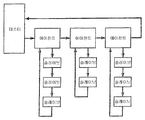
제3 기술은, 주요 링(즉, 전체 마스터를 제어하는 링)의 디바이스들의 각각이 슬레이브들의 서브-링에 대한 마스터로서 동작하는 에이전트(agent)인, 링들의 계층을 생성하는 것이다(도 1 참조). 특정 슬레이브들에 표적화된 커맨드들은 적절한 에이전트에 의해 인터셉트되고 표적화된 슬레이브를 포함하는 단일의 특정 서브-링에서 커맨드들로 해석된다. 흠결을 처리하는 제4 방법은, 차례로 비-링 기반 디바이스들을 제어하는, 에이전트들의 링을 갖는 것이다. 도 2의 예에 있어서, 각각의 에이전트는 전통적인 병렬 메모리 서브시스템을 제어한다.The third technique is to create a hierarchy of rings, each of which is an agent that acts as a master for the sub-rings of the slaves, each of the devices of the primary ring (i.e., the ring controlling the entire master) ). Commands targeted to particular slaves are intercepted by the appropriate agent and interpreted as commands in a single specific sub-ring including the targeted slave. A fourth way to deal with defects is to have a ring of agents, which in turn controls non-ring based devices. In the example of FIG. 2, each agent controls a conventional parallel memory subsystem.
이전의 그 해결책들은, 링 토폴로지의 인히어런트 장점들의 장점을 완전하게 취하는데 실패하거나 상기한 링 토폴로지 네트워크들의 문제점들을 적절히 다루는데 실패한다. 예를 들어, 링 오브 링스 토폴로지는, n 슬레이브들을 가진 시스템에 대해 통신 레이턴시를 감소시키기 위해 2 x sqrt(n) 더하기 에이전트내의 임의의 추가적인 스케쥴링 지연으로 계산되었다. 슬레이브당 지연을 감소시키는 것은 비례 상수를 감소시키지만, 총 통신 레이턴시는 여전히 링내의 디바이스들의 개수에 비례적인채로 남는다. 링내의 디바이스들의 개수를 소수로 제한하는 것은 총 통신 레이턴시를 제한하지만, 더 큰 시스템내의 상호 연결의 효용을 또한 제한한다.The prior solutions fail to take full advantage of the ring topology's inherent advantages or fail to properly address the problems of the ring topology networks described above. For example, a ring-of-ring topology has been computed with 2 x sqrt (n) plus any additional scheduling delays in the agent to reduce communication latency for systems with n slaves. Reducing the delay per slave reduces the proportional constant, but the total communication latency still remains proportional to the number of devices in the ring. Limiting the number of devices in the ring to a decimal number limits the total communication latency, but also limits the utility of the interconnect within a larger system.
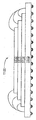
링 네트워크 성능을 향상시키기 위한 일부의 접근법들은 다수-칩 모듈의 사용을 포함한다. 다수-칩 모듈은, 하나 이상의 집적회로가 신호 핀들의 공통 세트와 함께 다수-칩 모듈이 장착되는 기판 또는 캐리어(carrier)에 수용되는, 패키징(packaging) 구조체이다. 더욱 정확한 설명이 상세한 설명 섹션에 제공된다. 다수-칩 모듈내의 집적회로들의 링-토폴로지 상호연결에의 간단한 적용은, 다수-칩 모듈내의 모든 디바이스들을 링내로 직렬 연결하는 것이다. 이러한 구성의 토폴로지 및 레이턴시는, 흡사 각각의 직접 회로가 그 자신의 패키지내에 있고 패키지들이 링내로 직렬 연결된 듯하다. 그 결과는, 접합 배선들에서의 최하위 디바이스내로 들어오고, 최하위 디바이스를 떠나고 그 위의 디바이스에 들어가며, 그리하여 스택 위로, 최상위 디바이스를 패키지와 연결하는 접합 배선들로 정점에 이르러 아웃바운드 링 세그먼트(outbound ring segment)를 형성하는, 링크를 볼 수 있는, 도 3에 도시된 것에 필적하는 패키지 단면도일 것이다.Some approaches to improving ring network performance include the use of multi-chip modules. The multiple-chip module is a packaging structure in which one or more integrated circuits are housed in a substrate or carrier on which the multi-chip module is mounted, with a common set of signal pins. A more precise description is provided in the Detailed Description section. A simple application to the ring-topology interconnections of integrated circuits in a multi-chip module is to serially connect all the devices in the multi-chip module into the ring. The topology and latency of such a configuration is such that each integrated circuit is in its own package and the packages are connected in series into the ring. The result is that the device enters the lowest device in the junction wirings, leaves the lowest device and enters the device above it, so that it reaches the top of the stack with the junction wires connecting the top device to the package and the outbound ring segment sectional view comparable to that shown in Fig. 3 in which the link can be seen, forming a ring segment.
도 3의 구성은 몇몇의 이유들로 덜 이상적이다. 먼저, 이 디바이스들이 단일 패키지로 보일지라도, 그것들은, 5개의 디바이스들만큼의 레이턴시를 나타내는, 논리적으로 5개의 디바이스들로서 존재한다. 2 번째, 디바이스들의 좌우 측부들의 착신 및 발신 세그먼트들의 이러한 특정 배열은, 편리하지 않을 수 있다. 일반적으로, n개의 디바이스들의 다수-칩 모듈은 물리적으로 하나의 디바이스를 나타내지만, 논리적으로 n개의 디바이스들을 나타낸다. 이러한 구성은, 다수-칩 모듈 접근법이 취해지지 않은, 큰 링들의 제한들의 일부를 다루도록 다수-칩 패키지내의 집적 회로들의 근접의 장점을 적절히 취하는데 실패한다.The configuration of Figure 3 is less ideal for several reasons. First, although these devices appear as a single package, they exist as five logical devices, representing a latency of five devices. Second, this particular arrangement of the incoming and outgoing segments of the left and right sides of the devices may not be convenient. Generally, a multiple-chip module of n devices physically represents one device, but logically represents n devices. This configuration fails to properly take advantage of the proximity of the integrated circuits in the multi-chip package to handle some of the limitations of large rings, where the multi-chip module approach is not taken.
본 발명의 실시예들은, (클러스터들로 불리는) 슬레이브 디바이스들의 그룹들이 병렬로 액세스되는, 클러스터 토폴로지의 링으로 불리는, 변형된 링 토폴로지에 존재한다. 몇몇 개소의 클러스터들은 링내의 단일 노드로서 작용한다. 이러한 구성의 덕택으로, 링 주위의 레이턴시는 클러스터들의 개수에 비례적이며 집적 회로들의 개수에는 비례적이지 않다. 데이터 통신과 관련된 전력 소모는 필적하는 링 네트워크에서보다 더 적고, 실시예들은 높은 정도의 내고장성을 제공한다. 토폴로지 상호 연결은 다수-칩 모듈 및/또는 개별적으로 패키지화된 집적 회로들의 사용에 잘 적합된다.Embodiments of the present invention exist in a modified ring topology, referred to as ring of cluster topologies, in which groups of slave devices (referred to as clusters) are accessed in parallel. Some clusters act as a single node in the ring. Thanks to this configuration, the latency around the ring is proportional to the number of clusters and not proportional to the number of integrated circuits. Power consumption associated with data communication is less than in comparable ring networks, and embodiments provide a high degree of fault tolerance. The topology interconnect is well suited for use with multi-chip modules and / or individually packaged integrated circuits.
본 발명의 실시예들에 따르면, 디바이스들의 그룹들은 병렬로 연결되고, 입력 및 출력 링 세그먼트들을 공유한다. 클러스터들은 하나 이상의 디바이스들을 포함하고, 실제로 클러스터당 디바이스들의 개수가 상대적으로 더 적을 것이다. 개시된 실시예들의 개수에 있어서, 입력 세그먼트에 도착하는 패킷들은 클러스터의 모든 디바이스들에 의해 수신되고 해석된다. 다른 실시예들에 있어서, 클러스터마다 무(無), 일부 또는 하나를 제외한 전부의 슬레이브들이 수면에 들어가거나 그게 아니면 디스에이블(disable)됨으로써, 그것들이 착신 패킷들을 입력 및 해석하지 않는다. 전체 실시예들에서, 관계없이, 클러스터의 슬레이브들은, 제어기들의 지도하에서 잠재적으로, 그것들 중 많아야 하나가 임의의 주어진 시간에서 출력 세그먼트를 활성적으로 드라이브하는 것을 보장하도록, 협력한다.According to embodiments of the present invention, groups of devices are connected in parallel and share input and output ring segments. Clusters include one or more devices, and the number of devices per cluster will actually be relatively small. In the number of disclosed embodiments, packets arriving at the input segment are received and interpreted by all devices in the cluster. In other embodiments, none of the clusters, some or all but one of the slaves enter the sleep surface or are otherwise disabled, so that they do not enter and interpret the incoming packets. In all embodiments, regardless of whether the slaves in the cluster cooperate, under the guidance of the controllers, potentially, at least one of them will actively drive the output segment at any given time.
본 발명의 실시예들에 따른 링 오브 클러스터 네트워크 토폴로지는, 입력 및 출력 세그먼트들에 링 구성으로 상호 연결된 복수의 슬레이브 디바이스들과 패킷화된 통신을 하는 제어기 디바이스를 포함하며, 슬레이브 디바이스들 중 적어도 일부가 병렬로 연결되어, 동일한 입력 및 출력 세그먼트들을 공유하는 클러스터를 형성한다. 적어도 하나의 실시예에 있어서, 클러스터 ID와 디바이스 ID의 조합에 의해 어드레스되는 디바이스들은, 그에 의해서, 요구되는 비트의 수와 관련 레이턴시를 극적으로 감소시킨다.A ring-of-cluster network topology according to embodiments of the present invention includes a controller device that performs packetized communications with a plurality of slave devices interconnected in a ring configuration to input and output segments, wherein at least some of the slave devices Are connected in parallel to form a cluster sharing the same input and output segments. In at least one embodiment, the devices addressed by the combination of cluster ID and device ID thereby dramatically reduce the number of bits required and the associated latency.
적어도 하나의 클러스터에 있어서, 클러스터 마스터로 설계된 디바이스는 클러스터의 슬레이브들을 조정하도록 작동함으로써, 클러스터내의 많아야 하나의 슬레이브가 출력 세그먼트를 드라이브한다. 클러스터의 슬레이브들은 단일 배선을 통해, 특정 슬레이브가 입력으로부터 출력 세그먼트로의 데이터 전송에 대해 준비되어 있다는 것을, 클러스터 마스터에 통신할 수 있다. 예를 들어, 클러스터의 슬레이브들은 단일의 다수-소스 단일-목적지 컨덕터를 통해 클러스터 마스터와 통신할 수 있다. 대안적으로, 클러스터 마스터는, 클러스터 마스터로 하여금 슬레이브들로부터 직접적으로 정보를 수신하지 않고 어느 슬레이브가 준비되었는가를 판정할 수 있게 하는, 클러스터내의 전체 슬레이브들에 표적화된 모든 커맨드들을 해석한다. 어떠한 경우에서든, 클러스터 마스터는, - 만약 있다면 - 어느 슬레이브들이 준비되었는가에 관계없이, 입력 세그먼트로부터 출력 세그먼트로 커맨드 패킷들을 전하도록 작동한다.In at least one cluster, a device designed as a cluster master operates to coordinate the slaves of the cluster so that at most one slave in the cluster drives the output segment. Slaves in the cluster can communicate to the cluster master through a single wire that a particular slave is ready for data transfer from the input to the output segment. For example, slaves in a cluster can communicate with a cluster master through a single, multiple-source single-destination conductor. Alternatively, the cluster master interprets all commands targeted to all slaves in the cluster, which allows the cluster master to determine which slave is ready without receiving information directly from the slaves. In any case, the cluster master acts to convey command packets from the input segment to the output segment, regardless of which slaves are ready, if any.
임의의 적절한 형태 또는 통합이 사용되더라도, 본 발명의 몇몇 실시예들은, 개별적인 클러스터들이 스택에서의 상이한 레벨들로 할당될 수 있다는 점에서, 다수-칩 모듈 구현들 및 수직 스태킹의 다른 형태들을 개발하는데 적합하다. 이것은 입력 세그먼트로 하여금 스택의 일측상에 모든 디바이스들에 도착할 수 있게 하고 출력 세그먼트로 하여금 스택의 다른 측으로부터 출발할 수 있게 한다. 대안적으로, 접합 배선들이 하나의 디바이스의 입력 세그먼트 접합 패드들(bonding pads)을 수직으로 인접한 디바이스의 접합 패드들에, 스택의 출력 세그먼트 측의 비교될 수 있는 세트의 연결들과 연결할 수 있다. 본 발명 네트워크의 다양한 디바이스들은, 본 발명이 이에 관하여 한정되지 않을지라도, 메모리 디바이스들일 수 있다.Although any suitable form or integration is used, some embodiments of the present invention may be used to develop multi-chip module implementations and other forms of vertical stacking in that individual clusters may be assigned different levels in the stack Suitable. This allows the input segment to arrive at all devices on one side of the stack and allows the output segment to depart from the other side of the stack. Alternatively, the junction wirings may connect the input segment bonding pads of one device to the junction pads of vertically adjacent devices, with a comparable set of connections on the output segment side of the stack. The various devices of the inventive network may be memory devices, although the invention is not limited in this respect.
이제 첨부 도면들에 대해, 예시로서, 언급이 이루어질 것이다. 유사 또는 동일한 참조 부호들이 유사한 구성 요소들을 나타내기 위해 상이한 도면들에서 사용되었을 수 있다.
도 1은 종래 기술의 토폴로지에 따른 링들의 링의 도면을 도시한다.
도 2는 종래 기술의 네트워크 토폴로지에 따른 서브시스템들의 링의 도면을 도시한다.
도 3은, 종래 기술에 따른 각각의 디바이스를 통과하는 링 토폴로지 네트워크를 가진 다수-칩 모듈의 도면을, 단면에서, 도시한다.
도 4는 디바이스들 중 하나가 제어기 또는 마스터인, 링 토포롤지 상호 연결 네트워크의 일 예의 도면을 도시한다.
도 5는 링 토폴로지 네트워크의 추가적인 도면을 도시하며, 본 도면은 입력 및 출력 세그먼트들과 관련되는 신호들을 도시한다.
도 6은 도 5의 링 네트워크의 슬레이브 디바이스내로 흐른 다음 그 밖으로 흐르는 커맨드 패킷 및 데이터 패킷의 타이밍도를 도시한다.
도 7은 커맨드 패킷의 내부 구조의 도면을 도시한다.
도 8은 일예의 실시예의 네트워크 토폴로지에 따른 클러스터들의 링의 제1 예의 도면을 도시한다.
도 9는 도 8의 그것과는 상이한 인트라-클러스터 통신 신호 배열을 갖는 클러스터들의 링의 제2 예의 도면을 도시한다.
도 10은 인트라-클러스터 링이 어떻게 디바이스 ID들을 통신하는 사용되는 임시 클러스터 마스터 상태를 조정하는데 사용되는가를 도시한다.
도 11A는, 디바이스들이 수직으로 스택되고 스택내의 모든 디바이스들이 클러스터 네트워크의 링내의 단일 클러스터를 형성하는 다수-칩 모듈의 도면을, 단면에서, 도시한다.
도 11B는, 디바이스들이 수직으로 스택되고 스택내의 모든 디바이스들이 클러스터 네트워크의 링내의 단일 클러스터를 형성하는 대안적인 다수-칩 모듈의 도면을, 단면에서, 도시한다.
도 12는 적어도 하나의 예에 따른 클러스터 토폴로지 상호 연결 네트워크의 링내에서의 클러스터의 도면을 도시한다.
도 13은 이전에 예시된 링 네트워크에 대한 단일 슬레이브의 도면을 도시한다.
도 14는 제1 또는 제2 예와는 상이한 인트라-클러스터 통신 신호들을 갖는 클러스터들의 링의 제3 예를 예시한다.Reference will now be made, by way of example, to the accompanying drawings. Similar or identical reference numerals may be used in different drawings to represent like elements.
Figure 1 shows a view of a ring of rings according to the prior art topology.
Figure 2 shows a diagram of a ring of subsystems according to the prior art network topology.
3 shows, in cross section, a diagram of a multi-chip module with a ring topology network passing through each device according to the prior art.
Figure 4 shows an example view of a ring topology interconnect network in which one of the devices is a controller or master.
5 shows a further illustration of a ring topology network, which shows signals associated with input and output segments.
Figure 6 shows a timing diagram of command packets and data packets flowing into and out of slave devices of the ring network of Figure 5;
7 shows a diagram of an internal structure of a command packet.
Figure 8 shows a diagram of a first example of a ring of clusters according to the network topology of an example embodiment.
Figure 9 shows a second example of a ring of clusters with an intra-cluster communication signal arrangement that is different from that of Figure 8;
Figure 10 shows how intra-clustering is used to adjust the temporary cluster master state used to communicate device IDs.
11A shows, in cross section, a diagram of a multi-chip module in which devices are stacked vertically and all devices in the stack form a single cluster in the ring of the cluster network.
11B shows, in cross section, a diagram of an alternative multi-chip module in which devices are stacked vertically and all devices in the stack form a single cluster in the ring of the cluster network.
12 shows a diagram of a cluster in a ring of a cluster topology interconnect network according to at least one example.
13 shows a diagram of a single slave for the ring network previously illustrated.
14 illustrates a third example of a ring of clusters having intra-cluster communication signals different from the first or second example.
본 발명의 실시예들은, 많은 디바이스들이, 상호 연결의 유용성 또는 유효성을 제한할 수 있는 링내에 포함될 때, 링 토폴로지 상호 연결들이 긴 레이턴시를 가질 수 있다고 하는 문제를 처리한다. 본 발명의 실시예들은 또한 기존의 링 네트워크 토폴로지들과 관련된 높은 전력 소모와 불충분한 내고장성과 관련된 문제들을 해결한다.Embodiments of the present invention address the problem that ring topology interconnects can have a long latency when many devices are included in a ring that can limit the usefulness or effectiveness of the interconnect. Embodiments of the present invention also solve problems associated with high power consumption and insufficient fault tolerance associated with existing ring network topologies.
본 발명의 실시예들은, 링내의 하나의 디바이스가 제어기인 링-토폴로지 전자 상호 연결들에 관련되지만, 본 발명에 이에 관하여 한정되지 않고 다른 배리에이션들의 링-토폴로지 네트워크들과 다른 시스템 및 서브시스템 타입들에 동등하게 적용될 것이다. 본 상세한 설명에 있어서, “마스터” 및 “제어기”라는 용어는 유의적으로 사용된다. 유사하게, 슬레이브들과 메모리들은, 본 발명의 실시예들을 주로 메모리 디바이스들인 슬레이브 디바이스들로 한정하지 않고 유의적으로 사용된다. 본 발명이, 전부 또는 일부의 비-메모리 슬레이브들을 포함하는 링들에도 동등하게 적용된다는 것이 이해된다. 추가적으로, 본 상세한 설명에 있어서, “상호 연결”, “네트워크” 및 “상호 연결 네트워크”는, 전자 또는 필적하는 디바이스들의 수집을 직접적으로 또는 간접적으로 연결하는 (하나 이상의 버스들내로 전체적으로 또는 부분적으로 수집되는) 배선들의 임의의 수집을 의미하도록 유의적으로 사용된다.Although embodiments of the present invention relate to ring-topology electronic interconnects in which one device in the ring is a controller, the present invention is not limited in this respect and may be applied to other systems and subsystem types of ring- . In this description, the terms " master " and " controller " are used interchangeably. Similarly, slaves and memories are used significantly without limiting the embodiments of the present invention to slave devices, which are mainly memory devices. It is understood that the present invention applies equally to rings comprising all or a portion of non-memory slaves. Additionally, in this detailed description, the terms " interconnect ", " network ", and " interconnect network " refer to a collection of electronic or matched devices that directly or indirectly connects (collectively or partially Lt; RTI ID = 0.0 > wirings < / RTI >
본 발명의 실시예들은 또한 전자 시스템들내의 다수-칩 모듈들을 사용하는 것에 관련된다. 많은 경우에 있어서, 실리콘의 다수의 부분품들은 단일 기판 또는 패키지로 함께 패키지화된다. 이것은 일반적으로, 실리콘의 부분품들이 스택에서 서로의 상부에 놓이는 수직으로, 또는 실리콘의 부분품들이 단일 패키지 또는 모듈내에서 서로 옆으로 놓이는 수평으로 양쪽으로 이루어진다. 실리콘의 다수의 부분품들(또는 더욱 일반적으로, 적어도 하나의 표면상에 제조된 전자 부품들을 가진 반도체 재료의 얇은 부분품)이 개별적으로 패키지화되고 그 다음에 패키지들이 스택에서 수직으로 장착되는 변형이 있다. 개시된 실시예가 함께 패키지화된 실리콘의 부분품들의 스택의 관점에서 기술되었을지라도, 적어도 예시의 실시예들이 이들 모든 경우에 적용된다.Embodiments of the present invention also relate to the use of multi-chip modules in electronic systems. In many cases, multiple pieces of silicon are packaged together into a single substrate or package. This is generally done either vertically with the parts of the silicon lying on top of each other in the stack, or horizontally with the parts of the silicon lying beside each other in a single package or module. There is a variation in which multiple pieces of silicon (or more generally, thin pieces of semiconductor material with electronic components fabricated on at least one surface) are individually packaged and then the packages are mounted vertically in the stack. Although the disclosed embodiments are described in terms of a stack of parts of silicon packaged together, at least illustrative embodiments apply in all of these cases.
본 개시에 있어서, “다수-칩 모듈”이라는 표현은 그러한 모든 패키징 또는 장착 기술들에 대한 일반적인 용어로 정의되며, 그러한 구조의 임의의 하나의 스타일 또는 타입에 한정되지 않는다. 또한, 본 개시에 있어서, 집적 회로는, 재료의 하나 이상의 표면내로 또는 그 표면상에 제조되는, 배선들, 트랜지스터들, 다이오드들, 및 센서들 - 이에 한정되지 않고 - 과 같은 전자 부품들을 가진 다른 반도체 재료 또는 실리콘의 부분품으로 정의된다. 디바이스 및 집적 회로라는 용어들은 여기서 유의적으로 사용된다.In this disclosure, the expression " multi-chip module " is defined in general terms for all such packaging or mounting techniques, and is not limited to any one style or type of such structure. Further, in this disclosure, an integrated circuit may include other electronic components, such as, but not limited to, wirings, transistors, diodes, and sensors, which are manufactured into or onto one or more surfaces of a material Semiconductor material or parts of silicon. The terms device and integrated circuit are used herein in significant ways.
“모듈”이라는 용어는, 집적 회로들이 그 위로 또는 그 내부로 장착되고, 모듈 그 자체가 궁극적으로 장착되는 매체 상의 컨덕터들에 대한 그 집적 회로들의 연결을 촉진하는 패키지 또는 기판 또는 유사한 구조체로 정의된다. 모듈 그 자체는 상호 연결 이외의 다른 구조체들을 포함하거나 포함하지 않을 수 있고, 집적 회로 이외의 그것내로 또는 상으로 장착되는 다른 부품들을 갖거나 갖지 않을 수 있다. 일부의 다수-칩 모듈들에 있어서, 접합 배선들은 집적 회로들을 각각의 다른 및/또는 모듈 그 자체에 연결한다. 다른 것들에 있어서, 집적 회로들은 모듈의 부분인 컨덕터들에 대한 직접 연결을 만든다. 예를 들어, 다수-칩 모듈의 하나의 공통적인 형태는, 몇몇의 집적 회로들이 수직 스택내로 서로의 정상위에 장착되고 접합 배선들이 집적 회로들을 모듈내의 컨덕터들에게 그리고 서로에게 연결하는 패키지이다.The term " module " is defined as a package or substrate or similar structure that facilitates the connection of integrated circuits to conductors on a medium on which the integrated circuits are mounted, or to which the module itself is ultimately mounted . The module itself may or may not include structures other than interconnects and may or may not have other components mounted into or onto it other than an integrated circuit. In some multi-chip modules, the junction interconnects connect the integrated circuits to each other and / or to the module itself. In others, the integrated circuits make a direct connection to the conductors that are part of the module. For example, one common form of multi-chip module is a package in which some integrated circuits are mounted at the top of each other in a vertical stack and the junction wires connect the integrated circuits to the conductors in the module and to each other.
이제, 예시의 링 토폴로지 상호 연결 네트워크(400)의 도면을 도시하는 도 4에 대해 언급된다. 네트워크(400)에 있어서, 디바이스로부터 디바이스로 흐르는 단방향성 링 주위로 정보가 흐른다. 이러한 경우에 있어서, 도면은, 디바이스들 중 하나가 메모리들 또는 다른 메모리 또는 비-메모리 슬레이브 디바이스들(411~415)을 액세스하는 제어기 또는 마스터 디바이스(410)인 링을 도시한다. 어드레스, 데이터 및 제어 정보는 모두, 동일 방향으로, 일반적으로 동일한 타이밍으로, 그리고 일반적으로 동일 컨덕터들상에 부분적으로, 링 주위를 흐른다. 도 5는 하나의 그러한 링 토폴로지 네트워크(500)의 신호들을 도시한다. 예시된 예에 있어서, 디바이스들(510~513)을 링내로 연결하는 링의 세그먼트들은 4개의 컨덕터들의 데이터 경로, 및 2개의 스트로브(strobe) 신호들을 포함한다. 정보는 패킷들내에서 링 주위로 흐른다. 도 4는 또한, 링내의 각각의 슬레이브가 고유한 어드레스를 갖는다는 것을 나타낸다. 예시된 경우에 있어서, 슬레이브 어드레스들은 제1 슬레이브가 제어기로부터 패킷들을 수신하는 0으로 시작하고, 거기서부터 최종 슬레이브까지 연속적으로 증가한다.Reference is now made to FIG. 4 which shows a drawing of an exemplary ring
예시된 네트워크의 적어도 일부의 경우에 있어서, 패킷들은, 슬레이브 디바이스에서 시작하여 제어기로 되 흘러가는 데이터 또는 제어기에서 시작하여 하나 이상의 슬레이브 디바이스들에 흘러가는 커맨드 패킷들을 포함한다. 이들 2 타입의 패킷들은 판독 데이터 패킷 및 커맨드 패킷으로 각각 불린다. 커맨드 패킷들은 디바이스 어드레스 및 하나 이상의 슬레이브들이 실행하는 커맨드를 포함한다. 커맨드 패킷의 디바이스 어드레스 부분은 패킷의 첫번째 바이트이고, 그것은 어느 디바이스 또는 디바이스들이 커맨드를 실행하는가를 특정한다. 커맨드의 의미에 따라, 커맨드 패킷의 나머지는, 표적 디바이스(들)내의 약간의 데이터 저장소의 어드레스 및 어쩌면 약간의 데이터도 포함할 수 있다.In the case of at least some of the illustrated networks, the packets include command packets starting at the controller or flowing to one or more slave devices, starting from the slave device back to the controller. These two types of packets are referred to as a read data packet and a command packet, respectively. The command packets include a device address and a command executed by one or more slaves. The device address portion of the command packet is the first byte of the packet, which specifies which device or devices execute the command. Depending on the meaning of the command, the remainder of the command packet may contain the address of some data store in the target device (s) and possibly even some data.
예시된 네트워크의 적어도 일부의 경우에 있어서, 데이터는 공통 클럭의 각각의 에지에 송신된다. 4개의 데이터 배선이 있음에 따라, 바이트는 각각의 클럭 주기로 송신된다. 도 6은 단일 슬레이브의 내로 그리고 밖으로 흐르는 커맨드 또는 데이터 패킷들과 2개의 스트로브들 사이의 관계를 도시한다. 커맨드 패킷이 슬레이브에 의해 수신될 때, Command Strobe In(CSI) 신호는 패킷의 시작 및 끝의 범위를 정한다. 데이터 패킷이 수신될 때, 착신 패킷은 Data Strobe In(DSI) 신호에 의해 범위가 정해진다.In at least some cases of the illustrated network, data is transmitted on each edge of the common clock. With four data wires, the bytes are transmitted in each clock period. Figure 6 shows the relationship between commands and data packets flowing into and out of a single slave and two strobes. When a command packet is received by the slave, the Command Strobe In (CSI) signal sets the beginning and end of the packet. When a data packet is received, the incoming packet is scoped by a Data Strobe In (DSI) signal.
데이터 및 커맨드 패킷의 양쪽에 대해서, 각각의 디바이스를 통하는 레이턴시는 소수의 클럭 사이클이고, 링상의 상이한 디바이스들이 상이한 플로우 쓰루 레이턴시들(flow through latencies)을 가질지라도, 그것은 아마도 - 반드시는 아니지만 - 디바이스의 설계의 부분으로서 고정된다. 도 6의 예에 은연중 예시된 슬레이브는, 커맨드 및 데이터 패킷의 양쪽이, 그것들이 입력 세그먼트에서 래치된 하나의 완전한 사이클 후에 출력 세그먼트 데이터 라인들(QO..3)상에 나타남에 따라, 하나의 사이클의 플로우-쓰루 레이턴시를 나타낸다. 출력 세그먼트상에서, 슬레이브는 커맨드 스트로브 아웃(Command Strobe Out) 및 데이터 스트로브 아웃(Data Strobe Out)을 상응하게 드라이브하는 것에 의해 출력 데이터 라인들상에 패킷들의 범위를 정한다.For both data and command packets, the latency through each device is a small number of clock cycles, and although different devices on the ring may have different flow through latencies, it is possible - but not necessarily - It is fixed as part of the design. The slave illustrated in the example of FIG. 6 implies that as both the command and data packets appear on the output segment data lines (QO. 3) after one complete cycle in which they are latched in the input segment, Represents the flow-through latency of the cycle. On the output segment, the slave schedules the packets on the output data lines by correspondingly driving a Command Strobe Out and a Data Strobe Out.
슬레이브 디바이스들은 커맨드 패킷들내의 커맨드들을 송신한다. 도 7은 도 6에 도시된 커맨드 패킷에 대응할 수 있는 커맨드 패킷들의 구조를 도시한다. 제1 바이트는, 커맨드를 실행하는 슬레이브의 디바이스 어드레스를 포함한다. 제2 바이트는 1 바이트 커맨드이다. 다음 바이트들의 수 및 의미들은 특정된 실제 커맨드에 좌우된다. 제어기가 결정하기 때문에, 다음의 바이트들은 제2 바이트내에 특정된 특정 커맨드에 좌우된다. 특히, 제어기가 슬레이브의 저장소에 데이터를 기입하기를 원할 때, 다음의 바이트들은 저장소의 슬레이브-로컬 어드레스 및 기입 데이터를 포함할 것이다. 도 7에 예시된 커맨드 패킷은 최상위 니블(nibble)을 먼저 송신한다. 제1 상승 에지에서, 비트들 4, 5, 6 및 7인 최상위 니블은 데이터 라인 DO, Dl, D2, 및 D3상에 송신된다. 제1 클럭 사이클의 2번째 절반 동안에, 비트들 0, 1, 2, 및 3인 제1 바이트의 최하위 니블은 대응 데이터 라인들상에 송신된다. 동일한 패턴이 커맨드의 모든 후속 바이트들에 대해 뒤 잇는다. 도 7의 3개의 커맨드 특정 바이트들에 예시된 바와 같이, 8 비트보다 더 많이 가진 어드레스의 경우에 있어서, 니블 및 바이트들의 시퀀스(sequence)는 최하위 바이트에 먼저 그리고 최상위 니블에 먼저 대응한다.The slave devices transmit commands in the command packets. FIG. 7 shows the structure of command packets that can correspond to the command packet shown in FIG. The first byte contains the device address of the slave executing the command. The second byte is a 1 byte command. The number and semantics of the following bytes depend on the actual command specified. As the controller determines, the following bytes depend on the particular command specified in the second byte. In particular, when the controller wishes to write data to the slave's repository, the following bytes will contain the slave-local address and write data of the repository. The command packet illustrated in FIG. 7 first transmits a top-level nibble. At the first rising edge, the most significant nibble of bits 4, 5, 6 and 7 is transmitted on the data lines DO, Dl, D2, and D3. During the second half of the first clock cycle, the least significant nibble of the first byte,
데이터 패킷들은 모든 종류의 데이터를 슬레이브로부터 제어기로 되돌려 통신하는데 사용될 수 있다. 제어기는, 슬레이브가 데이터를 제어기에 회신하기를원할 때, 데이터 패킷의 도착에 대해 슬레이브를 준비시키는 판독 데이터 전송 커맨드를 송신한다. 판독 데이터 전송 커맨드는, 제어기가, 슬레이브로 하여금 어떤 데이터를 제어기에게 회신하기를 원하는가를 나타낸다. 제어기가 요청된 데이터를 수신하도록 준비되어 있을 때, 그것은 데이터 패킷을 그것 내의 임의의 데이터와 더불어 링 아래로 송신한다. 데이터 패킷의 시작과 끝은 데이터 스트로브(Data Strobe) 신호들(대응적으로 CSO 및 CSI)의 상승 및 하강 에지에 의해 나타내어진다. 준비된 슬레이브가 판독 데이터 패킷의 도착을 검출할 때, 준비된 슬레이브는 패킷내의 착신 데이터를 무시하고, 그것을 출력 세그먼트상으로 복제하는 대신에, 상기 대신된 데이터에 의해 이전에 요청된 데이터를 드라이브한다. 적어도 일부의 예에 있어서, 전송될 데이터의 양은 판독 데이터 전송 커맨드에서 특정되지 않고, 대신 데이터 스트로브 인/아웃(Data Strobe In/Out)의 상승 및 하강 에지 사이의 클럭 사이클의 수에 의해 특정된다.Data packets can be used to communicate all sorts of data back to the controller from the slave. The controller sends a read data transfer command that prepares the slave for the arrival of the data packet when the slave wants to return the data to the controller. The read data transfer command indicates which controller the slave desires to return to the controller what data. When the controller is ready to receive the requested data, it transmits the data packet along with any data in it down the ring. The beginning and end of the data packet are indicated by the rising and falling edges of the Data Strobe signals (correspondingly CSO and CSI). When the prepared slave detects the arrival of the read data packet, the prepared slave ignores the incoming data in the packet and instead replicates it on the output segment, it drives the previously requested data by the substituted data. In at least some examples, the amount of data to be transferred is not specified in the read data transfer command, but instead is specified by the number of clock cycles between the rising and falling edges of the data strobe in / out.
본 발명의 실시예에 따른 링 오브 클러스터(클러스터 링) 토폴로지 네트워크에 있어서, 디바이스들은 입력 및 출력 링 세그먼트들을 공유하면서, 병렬로 연결된다. 클러스터들은 하나 이상의 디바이스들을 포함하고, 실제로 클러스터당 디바이스들의 수는 상대적으로 적을 것이다. 다수의 실시예들에 있어서, 입력 세그먼트에 도착하는 패킷들은 클러스터내의 모든 디바이스들에 의해 수신되고 해석된다. 다른 실시예들에 있어서, 클러스터마다 무(無), 일부 또는 하나를 제외한 전부의 슬레이브들이 수면에 들어가거나 그게 아니면 디스에이블됨으로써, 그것들이 착신 패킷들을 입력 및 해석하지 않는다. 일반적으로, 클러스터의 슬레이브들은, 제어기들의 지도하에서 잠재적으로, 그것들 중 많아야 하나가 임의의 주어진 시간에서 출력 세그먼트를 활성적으로 드라이브하는 것을 보장하도록, 협력한다. 이 명세서에 기술된 본 발명의 실시예들의 상이한 예들은, 주로 클러스터의 디바이스들이 이를 달성하기 위해 어떻게 협력하는가에 따라 변화한다.In a ring-clustering topology network according to an embodiment of the present invention, devices are connected in parallel, sharing input and output ring segments. Clusters include one or more devices, and the number of devices per cluster will actually be relatively small. In many embodiments, packets arriving at the input segment are received and interpreted by all devices in the cluster. In other embodiments, none of the clusters, some or all but one of the slaves enter the sleep surface or are otherwise disabled, so that they do not enter and interpret the incoming packets. In general, slaves in a cluster cooperate, potentially under the guidance of controllers, to ensure that at least one of them actively drives the output segment at any given time. The different examples of embodiments of the invention described herein vary mainly depending on how the devices in the cluster cooperate to achieve this.
도 8은 하나의 제어기(810) 및 4개의 클러스터들(811~814)의 링을 도시하는 클러스터 네트워크(800)의 예시적인 링의 도면이다. 클러스터들은 그 내부에 4개의 슬레이브들(820~823), 3개의 슬레이브들(830~832), 하나의 슬레이브(840), 및 2개의 슬레이브들(850~851)을 - 본 발명이 클러스터당 슬레이브들 또는 클러스터들의 임의의 특정 범위에 한정되지 않을지라도 - 각각 갖는다. 적어도 하나의 실시예에 있어서, 클러스터들은 고유의 클러스터 ID들이 주어진다. 도 8의 예에 있어서, 제1 클러스터는 클러스터 ID 0을 갖고 다음의 클러스터들은 1, 2, 및 3의 클러스터 ID들을 갖는다. 각각의 클러스터내에서, 디바이스들도 고유의 디바이스 ID들이 주어진다. 다시, 본 예에 있어서, 클러스터내의 제1 슬레이브는 0의 디바이스 ID가 주어지고, 다음의 슬레이브들(만약 있다면)은 1, 2, 3 등의 디바이스 ID들이 주어진다. 본 발명의 모든 실시예들에 있어서 “디바이스”라는 단어는 “별개(discrete)”라는 의미를 취하지 않아야 한다는 것에 주목한다. 다양한 실시예들이 별개의 디바이스들로 구현될 수 있지만, “디바이스들”은 동일 집적 회로상으로 집적될 수도 있다.Figure 8 is a drawing of an exemplary ring of
링내의 각 디바이스는 그로서, 그 클러스터 ID 및 그 디바이스 ID의 결합에 의해 고유하게 식별된다. 예를 들어, 클러스터당 16 슬레이브들까지의 16 클러스터들까지를 지원하는 네트워크는 4-비트 클러스터 ID 필드 및 4-비트 디바이스 ID 필드로 구성되는 1 바이트 디바이스 어드레스 필드를 가질 수 있다. 이러한 예에 있어서, 링내의 각 디바이스가 하나의 사이클의 플로우 쓰루 레이턴시를 가지면, 완전 장착 네트워크(fully populated network)는 16 사이클의 통신 레이턴시를 가질 것이다. 대조적으로, 동일한 수의 디바이스들을 가진, 또한 하나의 플로우 쓰루 레이턴시를 가진 도 4의 링 토폴로지 네트워크는, 256 사이클의 통신 레이턴시를 가질 것이다. 이러한 식으로, 링 오브 클러스터 토폴로지는, 매우 많은 디바이스들을 가진 시스템들을, 그것들의 레이턴시들을 선형적으로 합성하지 않고, 가능케 한다.Each device in the ring is uniquely identified by its combination of its cluster ID and its device ID. For example, a network supporting up to 16 clusters up to 16 slaves per cluster may have a one-byte device address field consisting of a 4-bit cluster ID field and a 4-bit device ID field. In this example, if each device in the ring has a flow through-run latency of one cycle, the fully populated network will have a communication latency of 16 cycles. In contrast, the ring topology network of FIG. 4 with the same number of devices and also with one flow through-run will have a communication latency of 256 cycles. In this way, the ring-of-clusters topology enables systems with very many devices, without linearly synthesizing their latencies.
도 8의 실시예에 있어서, 디바이스 ID 0을 가진 각각의 클러스터내의 디바이스는 클러스터 마스터로 불린다(그것은, 일부의 다른 디바이스 ID가 클러스터 마스터를 식별하는데 사용될 수 있다는 것이 이해될 것이다). 클러스터 마스터의 역할은, 클러스터내의 많아야 하나의 슬레이브가 발신 세그먼트를 드라이브하도록, 클러스터의 슬레이브들을 조정하는 것이다. 이러한 목적을 달성하기 위해, 클러스터내의 각각의 비-클러스터 마스터 슬레이브로부터 클러스터의 클러스터 마스터에 특별한 배선이 있을 수 있다. 이러한 배선은 특정 슬레이브가 준비되었다는 것을 클러스터 마스터에게 통신하는데 사용된다. 클러스터 마스터는, 데이터 패킷이 수신되고 클러스터내의 다른 슬레이브가 준비되었을 때를 제외하고 출력 세그먼트(스트로브들과 더불어 출력 데이터 버스)를 드라이브할 책임이 있다. 이러한 상황에 있어서, 클러스터 마스터는 데이터 스트로브 아웃(Data Strobe Out) 신호를 드라이브하고 데이터 아웃(Data Out) 신호들을 릴리즈(release)하여(즉, 그 출력 드라이버들이 높은 임피던스 상태로 들어감), 준비된 슬레이브가 그 자신의 판독 데이터를 데이터 패킷내로 삽입할 수 있다.In the embodiment of FIG. 8, a device in each cluster with a device ID of 0 is called a cluster master (it will be understood that some other device ID may be used to identify the cluster master). The role of the cluster master is to coordinate the slaves of the cluster so that at most one slave in the cluster drives the outgoing segment. To achieve this goal, there may be special wiring to the cluster master of the cluster from each non-cluster master slave in the cluster. This wiring is used to communicate to the cluster master that a particular slave is ready. The cluster master is responsible for driving the output segment (the output data bus along with the strobe), except when a data packet is received and another slave in the cluster is ready. In this situation, the cluster master drives the Data Strobe Out signal and releases the Data Out signals (i.e., the output drivers go into a high impedance state) Its own read data can be inserted into the data packet.
다른 실시예에 있어서, 단일 컨덕터는 클러스터내의 모든 슬레이브들을 연결한다. 그러한 실시예에 있어서, 하기의 조건이 유지될 것이다: 한 번에 전체 링내의 많아야 하나의 슬레이브가 준비될 수 있음으로써, 클러스터당 많아야 하나의 준비된 슬레이브가 있을 수 있다. 따라서, 단일의 다수-소스 단일-목적지 컨덕터(n:1 통신으로도 칭해짐)가 슬레이브가 준비되었다는 것을 마스터에게 표시하는데 사용될 수 있다.In another embodiment, a single conductor connects all the slaves in the cluster. In such an embodiment, the following conditions will be maintained: there can be at most one prepared slave per cluster, as at most one slave in the entire ring can be prepared at a time. Thus, a single, multiple-source single-destination conductor (also referred to as n: 1 communication) can be used to indicate to the master that the slave is ready.
또 다른 실시예에 있어서, 클러스터 마스터는 그 자신의 클러스터내의 모든 슬레이브들에 표적화된 커맨드들의 전부를 해석함으로써, 그 자신의 클러스터내의 임의의 다른 슬레이브들이 준비되는 때를 알며, 그래서 클러스터내의 다른 슬레이브들로부터 그것들이 개별적으로 준비되어 있는지 아닌지의 표시를 수신할 필요가 없다. 이러한 실시예는, 클러스터 마스터 디바이스가 클러스터내의 모든 다른 슬레이브들의 커맨드 세트를 선험적으로 아는 상황에서 가치가 있을 수 있다. 이것은 분명히 동질의 클러스터들내의 사례일 것이고, 클러스터내로 함께 결합되는 디바이스들이 완전하게 상이한 타입들의 것들 또는 동일한 타입의 상이한 버전들의 것들인, 이질의 클러스터들내에서는 덜 있음직한 사례일 것이다.In another embodiment, the cluster master interprets all of the targeted commands to all the slaves in its own cluster so that it knows when any other slaves in its cluster are ready, so that the other slaves in the cluster It is not necessary to receive an indication of whether they are individually prepared or not. This embodiment may be valuable in situations where the cluster master device a priori knows the command set of all the other slaves in the cluster. This will obviously be the case in homogeneous clusters and would be a less likely example in heterogeneous clusters where devices joined together into a cluster are of completely different types or of different versions of the same type.
모든 상기한 실시예들에 있어서, 준비된 슬레이브는 또한, 그것이 준비되고 데이터 패킷(Data Packet)이 도착하면, 데이터 스트로브 아웃(Data Strobe Out) 신호와 더불어 데이터 아웃(Data Out) 신호를 드라이브할 책임이 있을 수 있다. 하지만, 클러스터 마스터에는, 임의의 슬레이브들이 준비되었는가에 관계없이, 클러스터의 입력 세그먼트로부터 그 자신의 출력 세그먼트에 커맨드 패킷들을 전할 책임이 남아 있을 수 있다.In all of the above embodiments, the prepared slave is also responsible for driving a Data Out signal along with a Data Strobe Out signal when it is ready and a Data Packet arrives Can be. However, the cluster master may remain responsible for delivering command packets to its own output segment from the input segment of the cluster, regardless of whether any slaves are ready.
실시예들의 다른 비교될 수 있는 그룹에 있어서, 준비된 디바이스는 임시 마스터가 될 수 있고, 그것이 현재 판독 데이터를 데이터 패킷내로 삽입하는지의 여부에 관계없이, 커맨드 패킷들과 더불어 데이터 패킷들을 입력 세그먼트로부터 출력 세그먼트로 전할 책임을 가지게 될 수 있다. 클러스터 마스터는, 준비된 디바이스가 더 이상 준비되지 않게 될 때, 클러스터의 디바이스 0으로 또한 복귀할 수 있다. 네트워크 프로토콜의 특성에 따라, 이것은, 데이터 패킷의 끝에서, 준비된 슬레이브 디바이스가 판독 데이터 또는 약간 다른 조건을 삽입한 데이터 패킷의 끝 후에 새로운 커맨드 패킷의 시작에서 일 수 있다. 준비되지 않은 상태로의 이러한 복귀는, 이전에 기술된 방법들 중 임의의 방법에 의해 클러스터 마스터에 통신되거나 클러스터 마스터에 의해 은연중에 이해될 수 있다.In another comparable group of embodiments, the prepared device may be a temporary master and may output data packets along with command packets from an input segment, regardless of whether it inserts current read data into the data packet You may be responsible for transferring in segments. The cluster master may also return to device zero of the cluster when the prepared device is no longer ready. Depending on the nature of the network protocol, this may be at the beginning of a new command packet, after the end of the data packet, after the end of the data packet in which the prepared slave device inserted read data or slightly different conditions. This return to the unprepared state may be communicated to the cluster master by any of the previously described methods, or may be implicitly understood by the cluster master.
다른 대안에 있어서, 임시 마스터 상태는, 그것이 준비되지 않는 후에라도 준비된 디바이스와 남아 있으며, 클러스터내의 일부 다른 슬레이브가 준비되는 그러한 시간까지 그러하다. 그 시점에, 임시 마스터 상태는 새롭게 준비된 디바이스로 이동하고, 클러스터내의 일부 다른 디바이스가 준비될 때까지 그 디바이스와 남아 있는다. 이러한 실시예들의 세트에 있어서, 준비된 상태의 통신은 단일 컨덕터들의 링에 의해, 또는 공유된 배선에 의해 통신될 수 있다. 전자의 경우에, 새롭게 준비된 디바이스는, 인트라-클러스터 단일-컨덕터 링 아래로 상승 에지를 송신한다(도 9 참조). 링크내의 각 디바이스는 상승 에지를 인트라-클러스터 링내의 다음 슬레이브에 전한다. 그 상승 에지가 현재의 임시 마스터에 도달할 때, 그것은 임시 클러스터 마스터 상태를 포기하고 상승 에지를 클러스터내의 다음 슬레이브에 전한다. 상승 에지가 새롭게 준비된 슬레이브에 돌아갈 때, 그것이 이제 임시 클러스터 마스터 상태를 가지며 그것이 이제 커맨드 및 데이터 패킷들을 클러스터의 출력 세그먼트에 전할 책임을 갖는다는 것이 보증된다. 준비된 상태와 임시 클러스터 마스터 상태를 통신하고 중재하기 위한 다른 시그널링 규약과 상호 연결 토폴로지는 일반적인 기술 중 하나에 명백할 것이다.In another alternative, the provisional master state remains until the time that it remains with the prepared device even after it is not ready, and some other slave in the cluster is ready. At that point, the temporary master state moves to the newly prepared device and remains with that device until some other device in the cluster is ready. In this set of embodiments, the communication in the ready state can be communicated by a ring of single conductors, or by a shared wiring. In the former case, the newly prepared device sends a rising edge below the intra-cluster single-conductor ring (see FIG. 9). Each device in the link conveys the rising edge to the next slave in the intra-cluster ring. When the rising edge reaches the current temporary master, it abandons the temporary cluster master state and conveys the rising edge to the next slave in the cluster. When the rising edge returns to the newly prepared slave, it is now guaranteed that it has a temporary cluster master state and that it is now responsible for transferring command and data packets to the cluster's output segment. Other signaling protocols and interconnection topologies for communicating and arbitrating prepared state and temporary cluster master state will be apparent to one of ordinary skill.
적어도 하나의 실시예에 있어서, 하나의 패킷의 시작은 적어도 2분 1 사이클만큼 이전의 패킷의 끝을 뒤 따른다. 이러한 갭(gap)은, 클러스터들이, 전송되는 데이터가 없는 동안, 클러스터의 출력 세그먼트의 일부의 요소들의 전부를 드라이브하기 위한 책임을 전가할 기회가 있음을 보장한다.In at least one embodiment, the beginning of one packet follows the end of the previous packet by at least a quarter of a cycle. This gap ensures that the clusters have an opportunity to pass on responsibility for driving all of the elements of a part of the cluster's output segment while there is no data to be transmitted.
대안적으로, 발신 세그먼트에 사용되는 시그널링 기술은 와이어드(wired)-곱(AND) 타입이다. 이러한 타입의 시그널링 기술로, 하나 이상의 디바이스들이 신호를 드라이브하면, 수신된 값은 2개의 드라이브된 값들의 논리 곱(AND)이다. 예를 들어, 외부 풀-업(pull-up) 저항기를 가진 개방-컬렉터(open-collector) 드라이버는, 와이어드-곱(AND) 시그널링 기술의 일 예이다: 2개의 드라이빙 디바이스들 중 어느 한쪽이 출력 신호를 로우(low)로 풀(pull)하면, 수신되는 값은 로우이다. 다른 와이어드-곱(AND) 및 그것들의 상대인 와이어드-합(OR) 시그널링 기술들은 당업자에게 잘 알려져 있다.Alternatively, the signaling technique used for the outgoing segment is a wired-multiply (AND) type. With this type of signaling technique, when one or more devices drive the signal, the received value is the logical product of two driven values (AND). For example, an open-collector driver with an external pull-up resistor is an example of a wired-product (AND) signaling technique: either one of the two driving devices outputs When the signal is pulled low, the received value is low. Other wired-products (AND) and their relative wired-sum (OR) signaling techniques are well known to those skilled in the art.
이 실시예들에 있어서, 클러스터 마스터는, 바로 도 8의 네트워크에서와 같이, 착신 커맨드 및 데이터 패킷들을 출력 세그먼트에 복사하면서, 계속해서 출력 세그먼트를 드라이브한다. 비-클러스터 마스터 슬레이브들은 오로지, 제어기에 의해 그곳에 위치되는 데이터를 오버라이트(overwrite)하면서, 판독 데이터를 발신 세그먼트 데이터 출력 라인들상으로 드라이브한다. 제어기가 모든 발신 데이터 패킷들을 1들로 채움으로서, 데이터 패킷내의 데이터가 준비된 슬레이브로부터의 판독 데이터와 논리 곱(AND)될 때, 제어기에 도달하는 결과적인 데이터는 정확히 준비된 디바이스로부터의 판독 데이터이다. 슬레이브들이 그것들의 클러스터-상대와 통신할 필요는 없다. 그것들은, 그것들이 클러스터 마스터인지 아닌지의 여부만을 알아챌 필요가 있다. 다른 와이어드-타입의 시그널링 기술들을 이용하는 비교될 수 있는 실시예들에 있어서, 제어기로부터 발신 데이터 패킷들내로 삽입되는 초기 값은 시그널링 기술에 의해 구현되는 논리 기능에 대한 식별 값으로 채워진다.In these embodiments, the cluster master continues to drive the output segment, copying the incoming command and data packets to the output segment, just as in the network of FIG. The non-cluster master slaves only drive the read data onto the outgoing segment data output lines, overwriting the data located there by the controller. As the controller fills in all outgoing data packets with ones, the resultant data arriving at the controller is the read data from the device being correctly prepared when the data in the data packet is ANDed with the read data from the prepared slave. Slaves do not need to communicate with their cluster-counterparts. They need to know only whether they are cluster masters or not. For comparable embodiments using other wired-type signaling techniques, the initial value inserted into the outgoing data packets from the controller is filled with the identification value for the logic function implemented by the signaling technique.
모든 실시예들에 있어서, 링내의 각 디바이스는 어드레스로 고유하게 식별된다. 적어도 하나의 실시예에 있어서, 앞서 기술된 바와 같이, 슬레이브들은 각각의 클러스터내에서 고유한 디바이스 ID를 갖는다. 적어도 하나의 실시예에 있어서, 각각의 슬레이브는, (클러스터 ID 및 디바이스 ID의 결합에서의 비트들의 수와 수적으로 동등한) 전용의 ID 입력 라인들상의 전압을 검출하는 것에 의해 그 자신의 클러스터 ID 및 디바이스 ID를 판정한다.In all embodiments, each device in the ring is uniquely identified by an address. In at least one embodiment, as described above, the slaves have device IDs unique within each cluster. In at least one embodiment, each slave is configured to detect its own cluster ID by detecting the voltage on dedicated ID input lines (which is numerically equivalent to the number of bits in the combination of cluster ID and device ID) The device ID is determined.
디바이스 ID들이, 클러스터내의 디바이스들의 각각을 통해 데이지 체인되어 있는(daisy chained) 리셋 신호의 장점을 취하는 것에 의해 리셋 후에 설정될 수 있다는 것에 주목한다. 모든 슬레이브는 리셋 인(Reset In) 신호 및 리셋 아웃(Reset Out) 신호의 양쪽을 갖는다. 클러스터 마스터 슬레이브의 리셋 인(Reset In)은 글로벌 시스템 리셋(global system reset)에 연결될 수 있다. 각각의 클러스터 마스터의 리셋 아웃(Reset Out) 신호는, 결국 1 등등의 디바이스 ID가 될 그들 개개의 클러스터내의 슬레이브들의 리셋 인(Reset In) 신호에 연결될 수 있다. 링 서브시스템은 리셋의 단순한 하이에서 로우의 천이로 리셋 상태를 벗어난다. 각 클러스터내의 제1 디바이스는, 그것이 대응 클러스터 마스터이고 그 자신의 디바이스 ID가 0이라는 표시로서 리셋 인(Reset In)상에서의 그 단순한 단일의 천이를 인식한다. 각각의 클러스터 마스터는 그 다음으로, 일련의 3 천이들 - 하이에서 로우, 로우에서 하이 그 다음에 하이에서 다시 로우 -로 리셋 아웃(Reset Out)을 어서트 정지(de-assert)시킨다. 다음 디바이스는, 그것이 클러스터내의 제2 디바이스이고 따라서 그 자신의 디바이스 ID가 1 이라고 하는 표시로서 리셋 상의 일련의 3 천이들을 인식한다.Note that device IDs can be set after reset by taking advantage of a daisy chained reset signal through each of the devices in the cluster. All slaves have both a Reset In signal and a Reset Out signal. The Reset In of the cluster master slave can be connected to a global system reset. The Reset Out signal of each cluster master may be connected to a Reset In signal of slaves in their respective clusters which will eventually become a Device ID of one or the like. The ring subsystem goes out of reset state with a transition of low from a simple high of reset. The first device in each cluster recognizes its simple single transition on the Reset In as an indication that it is the corresponding cluster master and its own device ID is zero. Each cluster master then de-asserts a Reset Out from high to low, then high to low again in a series of three-way highs. The next device recognizes a series of three trials on the reset as an indication that it is the second device in the cluster and therefore its device ID is one.
각각의 디바이스가 그 자신의 디바이스 ID를 판정하기 위해 리셋 인(Reset In)의 천이들의 수를 계수하고, 그 다음으로, 다음 디바이스가 1 더 큰 디바이스 ID를 할당받는 것을 보장하기 위해 2 만큼 천이들의 수를 증가시키면서, 이러한 패턴이 계속된다. 디바이스 ID들이 모두 설정된 후에, 클러스터 ID 값들은, 디바이스 ID들이 설정될 수 있는 동일한 방식으로 설정될 수 있다: 링이 리셋된 후에, 제어기는 모두 영들을 가진 특별한 패킷을 링 아래로 송신한다. 전체 네트워크내의 모든 슬레이브는 그 자신의 클러스터 ID로서의 값을 취한다. 각 클러스터의 클러스터 마스터는, 다음 클러스터에 송신하기 전, 특별한 패킷내의 값을 증가시킨다. 대안적으로, 제어기는 일부 다른 값으로 특별한 패킷을 채울 수 있고, 클러스터 마스터들은 다음 클러스터의 클러스터 ID를 생성하기 위해 특별한 패킷내의 값에 증가, 감소 또는 그 외의 작용을 할 수 있다. 당업자라면 리셋 신호의 의미가 발명상의 중대성의 것이 아니라는 것을 인식할 것이다.Each device counts the number of transitions in Reset In to determine its own device ID and then counts the number of transitions This pattern continues, increasing the number. After all the device IDs are set, the cluster ID values can be set in the same way that the device IDs can be set: after the ring is reset, the controller sends a special packet with all zeros down the ring. All slaves in the entire network take a value as their own cluster ID. The cluster master in each cluster increases the value in the special packet before sending it to the next cluster. Alternatively, the controller may populate the special packet with some other value, and the cluster masters may increment, decrement, or otherwise act on the value in the special packet to generate the cluster ID of the next cluster. Those skilled in the art will appreciate that the meaning of the reset signal is not critical to the invention.
도 10은 다른 예시적인 실시예에 따른 다른 링 오브 클러스터 네트워크(1000)의 도면을 도시한다. 네트워크(1000)는 제어기(1010) 및 3개의 클러스터들(1011~1013)을 포함한다. 클러스터들은 그 내부에 4개의 슬레이브들(1020~1023), 3개의 슬레이브들(1030-1032), 및 2개의 슬레이브들(1040~1041)을 - 본 발명이 클러스터당 슬레이브들 또는 클러스터들의 임의의 특정 범위에 한정되지 않는 다는 것이 다시 주목되더라도 - 각각 갖는다. 도 10의 구성에 있어서, 임시 클러스터 마스터 상태를 중재하는데 사용되는 인트라-클러스터 링은 디바이스 ID들을 통신하는데 사용된다. 전체 슬레이브들은 리셋 인(Reset In) 입력을 갖는다. 클러스터 마스터가 아닌 모든 슬레이브들은 그라운드된 그 입력들을 갖는다. 클러스터 마스터들은 글로벌 링 리셋에 연결되는 그들의 리셋 인(Reset In) 입력들을 갖는다. 리셋 인(Reset In)의 하이에서 로우의 천이의 인식시에, 클러스터 마스터들은 그들의 상태를 클러스터 마스터로서 인식하고, 그들의 디바이스 ID들을 영으로 설정하며, 인트라-클러스터 링 아래로 비교될 수 있는 성장 펄스 스트림을 송신하여 클러스터내의 모든 다른 디바이스들의 클러스터 ID들을 순차적으로 초기화시킨다.FIG. 10 shows a diagram of another ring of
다른 실시예에 있어서, 클러스터 마스터에서의 각 클러스터내의 그 디바이스의 표시는 전용 신호의 사용에 의해 하드 와이어드된다(hard wired). 클러스터 ID들이, 클러스터 ID들을 설정하기 위한 앞서 기술된 절차를 이용하여, 먼저 설정되고, 다시금 디바이스의 ID들을 설정하기 위한 앞서 기술된 절차에 의해서, 디바이스 ID들의 설정이 뒤 따른다. 다른 실시예에 있어서, 리셋 신호들로부터 분리된, 전용의 신호들의 세트 및 임시 클러스터 마스터 중재 신호들이, 당업자에게 명백한 기술들에 따라서 디바이스 ID들을 초기화시키는데 사용된다.In another embodiment, the indication of the device in each cluster at the cluster master is hard wired by use of a dedicated signal. The cluster IDs are set first using the procedure described above for setting the cluster IDs, followed by the setting of the device IDs by the procedure described above for setting the device IDs again. In another embodiment, a set of dedicated signals and temporary cluster master arbitration signals separate from the reset signals are used to initialize the device IDs according to techniques that are obvious to those skilled in the art.
이제 도 11A를 참조하여 보면, 스택의 모든 디바이스들(1110~1113)이 단일 클러스터를 구성하는, 수직 스택의 다수-칩 모듈(1100)이 도시된다. 입력 세그먼트가 일측에서 모든 디바이스들에 도착하고 출력 세그먼트가 모듈의 타측에서 출발한다. 도 11B는, 접합 배선들이 하나의 디바이스상의 입력 세그먼트 접합 패드들을 수직으로 인접한 디바이스상의 접합 패드들에 연결하고, 스택의 출력 세그먼트 측상에 필적하는 연결들의 세트를 가진다는 점에서 모듈(1100)과는 상이한 대안적인 모듈(1150)내의 동일한 스택의 디바이스들(1110~1113)을 도시한다. 그러한 구현에 있어서, 스택은, 하나의 클러스터, 하나 이상의 클러스터들 및 제어기 등등 보다 더 많이 포함할 수 있다.Referring now to FIG. 11A, a
적어도 하나의 알려진 링 네트워크에 있어서, 임의의 디바이스가 고장이면, 제어기와 모든 디바이스들 사이의 라운드-트립(round-trip) 통신이 중지된다. 본 발명의 실시예들에 따르면, 하지만, 비-클러스터 마스터가 완전히 고장이면, 통신은 계속 방해받지 않을 것이다. 고장난 디바이스는 결코, 그것이 준비되었다는, 그 자신의 표시자를 어서트(assert)하지 않을 것이다. 고장난 디바이스가, 그것이 준비되었다고 계속해서 어서트하도록 고장이 나면, 그 클러스터의 디바이스들과 통신할 능력이 억제될 수 있다. 하지만, 다른 클러스터들과의 통신은 영향 받지 않을 것이다. 클러스터 마스터가 고장이면, 라운드-트립 통신이 중단될 것이다.In at least one known ring network, if any device fails, the round-trip communication between the controller and all the devices is stopped. According to embodiments of the present invention, however, if the non-cluster master is completely failed, communication will not continue to be disturbed. A failed device will never assert its own indicator that it is ready. If a failed device fails to continue asserting it is ready, the ability to communicate with the devices in that cluster may be suppressed. However, communication with other clusters will not be affected. If the cluster master fails, round-trip communication will be interrupted.
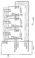
도 12는 링당 임의의 하나의 디바이스의 고장을 무릅쓰고 기능할 수 있는 대안적인 실시예를 나타낸다. 그것에 있어서, 각각의 슬레이브는 (넥스트 아웃(Next Out) 및 스킵 아웃(Skip Out)으로 불리는) 2개의 인트라 클러스터 출력들과, 넥스트 인(Next In) 및 스킵 인(Skip In)으로 불리는 2개의 인트라 클러스터 입력들을 갖는다. 각 디바이스의 넥스트 아웃(Next Out)은, 클러스터내에서 논리적으로 이웃한 디바이스의 넥스트 인(Next In)에 연결되며, 최종 디바이스의 넥스트 아웃(Next Out)은 제1 디바이스 - 그 디바이스는 일반적으로 클러스터 마스터임 - 의 넥스트 인(Next In)에 연결된다. 다음 신호들은 그로서 단순한 인트라 클러스터 링을 형성한다.Figure 12 shows an alternative embodiment that can function in the event of failure of any one device per ring. In this regard, each slave has two intracluster outputs (called Next Out and Skip Out) and two intra-cluster outputs called Next In and Skip In. Have cluster inputs. The Next Out of each device is connected to the Next In of the logically neighboring devices in the cluster and the Next Out of the last device is the first device- It is connected to the Next In of the master. The following signals then form a simple intracluster ring.
각 디바이스의 스킵 아웃(Skip Out)은, 클러스터내의 하나 걸러 이웃하는 디바이스의 스킵 인(Skip In)에 연결된다. 최종 슬레이브에 이웃한 디바이스의 스킵 아웃(Skip Out)은 클러스터내의 제1 슬레이브의 스킵 인(Skip In)에 연결되고, 클러스터내의 최종 슬레이브의 스킵 아웃(Skip Out)은 클러스터내의 제2 슬레이브의 스킵 인(Skip In)에 연결된다. 이러한 내고장 실시예에 있어서, 각각의 내고장 클러스터는 그 내부에 적어도 2개의 슬레이브를 가지며, 따라서 스킵(Skip) 신호들을 통해 그것에 연결되는 하나 걸러 이웃하는 슬레이브가 어느 것인지가 항상 명백하다. 클러스터내의 1번째의 2개의 슬레이브들의 리셋 인(Reset In) 신호들은, 제1 리셋(Primary Reset) 및 백업 리셋(Backup Reset)으로 불리는, 2개의 링-글로벌 신호들에 연결된다.The Skip Out of each device is connected to the Skip In of every neighboring device in the cluster. The Skip Out of the device neighboring the last slave is connected to the Skip In of the first slave in the cluster and the skip out of the last slave in the cluster is the skip of the second slave in the cluster (Skip In). In this fault tolerant embodiment, it is always clear that each fault cluster has at least two slaves within it, and thus every other neighboring slave connected to it via the Skip signals. The Reset In signals of the first two slaves in the cluster are connected to two ring-global signals, referred to as a Primary Reset and a Backup Reset.
디바이스 ID들의 초기화 및 할당은 다음과 같이 진행한다. 제어기는 제1 리셋(Primary Reset)을 상승시키고, 그것이 각 클러스터의 제1 슬레이브에 의해 인식될 수 있는 충분한 시간 동안 그것을 하이(high)로 유지한다. 이러한 제1 슬레이브는 그 다음에 그 자신을 클러스터 마스터로 할당하고 그 자신의 디바이스 ID를 0으로 설정한다. 그것은 그 다음에 넥스트 아웃(Next Out) 및 스킵(Skip Out)을 상승시키고, 클러스터내의 모든 다른 슬레이브들은 스킵 인(Skip In) 또는 넥스트 인(Next In)의 하이 레벨을 스킵 아웃(Skip Out) 및 넥스트 아웃(Next Out)으로 전파하고 그 자신들을 리셋 상태로 둔다.Initialization and allocation of device IDs proceeds as follows. The controller raises a primary reset and keeps it high for a sufficient time to be recognized by the first slave of each cluster. This first slave then assigns itself to the cluster master and sets its own device ID to zero. It then raises the Next Out and Skip Out and all other slaves in the cluster skip High in the Skip In or Next In levels, Propagate to Next Out, and put themselves in a reset state.
제1 리셋(Primary Reset)이 하강할 때, 클러스터 마스터는 하강 에지를 인식하고, 3 천이들의 펄스 트레인(pulse train)을 넥스트 아웃(Next Out)상에서 제2 디바이스에 송신하고(하이에서 로우, 로우에서 하이, 그 다음에 다시 하이에서 로우), 5 천이들의 펄스 트레인을 스킵 아웃(Skip Out)상에서 송신한다. 클러스터내의 모든 다른 슬레이브는 하기의 규칙들을 따른다: 넥스트 인(Next In) 또는 스킵 아웃(Skip Out)이 연장된 기간동안 하이일 때, 리셋 상태로 들어가고 슬레이브의 디바이스 ID 및 클러스터 ID를 소거한다; 리셋 상태에 있을 때 넥스트 인(Next In) 및 스킵 인(Skip In)의 양쪽의 천이 트레인(transition train)을 감시한다. 천이 트레인이 어느 한쪽의 신호에 도착하면, 천이들의 수를 계수하고, 1을 빼고 2로 나누며, 디바이스 ID를 그 결과로 설정한다. 어느 한쪽 입력상의 후속 천이 트레인들을 무시한다. 디바이스 ID가 설정되면, 넥스트 아웃(Next Out)상에서 길이 2 × 디바이스 ID + 3의 넥스트 아웃(Next Out)상의 천이 트레인을 송신하고 스킵 아웃(Skip Out)상에서 길이 2 × 디바이스 ID + 5 천이들의 천이 트레인을 송신한다. 그 후, 일반적인 동작 모드에 들어가고 앞서 기술된 바와 같이 클러스터 ID를 설정하기 위해 특별한 패킷에 대해 착신 세그먼트를 감시한다. 클러스터 마스터는, 그 자신의 클러스터내의 디바이스들의 수를 알기 위해서, 그 자신의 넥스트 인(Next In) 및 스킵 인(Skip In)상에서 트레인 천이들을 감시할 수 있다.When the Primary Reset falls, the cluster master recognizes the falling edge and sends a pulse train of three orders of magnitude to the second device on the Next Out (high to low, low And then back to high in the high), a pulse train of five orders of magnitude is sent on Skip Out. All other slaves in the cluster follow the following rules: When Next In or Skip Out is high for an extended period of time, enter the reset state and clear the device ID and cluster ID of the slave; Monitors the transition trains of both Next In and Skip In when in the reset state. When a transition train arrives at either signal, counts the number of transitions, subtracts 1, divides by 2, and sets the device ID as the result. Ignores subsequent transition trains on either input. When the device ID is set, a transition train on a Next Out with a length of 2 x Device ID + 3 is sent on Next Out, and a transition of length 2 x Device ID + 5 shifts on Skip Out Train. It then enters a normal mode of operation and monitors the incoming segment for a particular packet to set the cluster ID as described above. The cluster master may monitor the train transitions on its own Next In and Skip In to know the number of devices in its own cluster.
이후, 제어기가 패킷이 링 주위를 끝까지 가는지를 확인할 수 없으면, 제1 클러스터 마스터들 중 하나가, 그것이 정상적인 동작을 막는 방식으로 고장났다는 점에서, 죽어 있을 가능성이 있다. 그 경우에 있어서, 그것은 백업 세트(Backup Set)를 이용하여 재 초기화되어야 한다. 이것은 각 클러스터내의 제2 슬레이브를 디바이스 ID 0을 가진 클러스터 마스터로 설정할 것이다.Thereafter, if the controller can not verify that the packet goes all the way around the ring, it is likely that one of the first cluster masters is dead in that it has failed in a way that prevents normal operation. In that case, it must be reinitialized using a Backup Set. This will set the second slave in each cluster as the cluster master with
이러한 실시예는 링당 하나의 죽은 슬레이브가 있는 동작을 촉진한다. 클러스터당 하나의 슬레이브 고장까지도 무릅쓰고 기능하는 관련 실시예는, 제어기가 클러스터 바이(by) 클러스터 기초로 제1 리셋 또는 백업 리셋을 사용할 능력을 갖는다는 점을 제외하고 동일하다. 그와 같이, 제1 클러스터상의 제1 슬레이브와 제2 클러스터상의 제2 디바이스가 모두 나쁜 상태이면, 제어기는 그럼에도 2개의 클러스터들내의 클러스터 마스터들을 그에 맞게 분리 할당할 수 있다. 이러한 개념의 확장을 활용하는 추가적인 실시예들은 클러스터당 다수의 디바이스 고장이 있는 동작을 촉진할 가능성이 있다.This embodiment facilitates operation with one dead slave per ring. A related embodiment that works well beyond one slave failure per cluster is the same, except that the controller has the ability to use a first reset or a backup reset on a cluster by cluster basis. As such, if both the first slave on the first cluster and the second device on the second cluster are in a bad state, the controller can nevertheless separately allocate the cluster masters in the two clusters accordingly. Additional embodiments utilizing this extension of the concept are likely to facilitate operation with multiple device failures per cluster.
도 12의 내고장 클러스터가 이전에 기술된 동일한 프로토콜에 의해 링내의 이전의 클러스터(또는 제어기) 및 다음의 클러스터(또는 제어기)와 통신한다 - 단일 링은 내고장 클러스터들과 비-내고장 클러스터들의 혼합을 포함할 수 있다.The fault cluster of FIG. 12 communicates with the previous cluster (or controller) and the next cluster (or controller) in the ring by the same protocol as previously described-a single ring includes a mix of fault clusters and non-fault clusters can do.
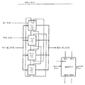
도 13은, 예시적인 실시예들에 따라 네트워크들내에서 사용될 수 있는, “Non-volatile Memory System”이라는 제목의 미국 특허 가출원 제60/902,003호에 추가적으로 상세히 개시되어 있는 디바이스(1300)의 도면이다. 디바이스(1300)는, 본 경우에서, 입력 데이터 버스로 이루어지는 입력 포트, 및 정보가 입력 데이터 버스상에서 흐를 때를 표시하는데 사용되는 2개의 입력 스트로브 신호들을 갖는다. 데이터 버스 세그먼트들이 4 비트 폭으로 도시되었지만, 본 발명이 데이터 버스 폭에 관계없이 동작될 수 있음에 따라, 데이터 폭은 1 비트 이상의 임의의 폭일 수 있다. 디바이스는 출력 데이터 버스로 이루어지는 출력 포트 및 데이터가 출력 데이터 버스 상으로 슬레이브에 의해 드라이브되기 시작될 때를 표시하도록 하는 2개의 출력 스트로브 신호들을 갖는다. 다시, 이러한 모든 다른 도면들내의 4 비트의 출력 데이터 버스 폭은 순전히 예시이며 본 발명의 권리 범위를 나타내지 않는다. 입력 포트, 출력 포트에 추가로, 이러한 특정 디바이스는 소수의 추가적인 비-파워(non-power) 신호들을 갖는다. 디바이스는 또한, 클럭 입력(본 경우에서는, 싱글 엔디드(single ended)이지만, 또한 잠재적으로 차동의), 디바이스를 알려진 초기 상태로 초기화하도록 하는 리셋 입력, 및 입력과 출력 포트들을 턴온시키는데 사용되고 그에 의해 링 주위로의 통신을 가능케 하는 칩 인에이블(Chip Enable) 입력을 갖는다.Figure 13 is a drawing of a
도 14는 다른 예시적인 실시예에 따라 다른 링 오브 클러스터 네트워크(1400)의 도면을 도시한다. 네트워크(1400)는 제어기(1410) 및 4개의 클러스터들(1411~1414)을 포함한다. 클러스터들은 - 본 발명이 클러스터당 슬레이브들 또는 클러스터들의 임의의 특정 범위에 한정되지 않는 것이 다시 주목되더라도 - 그 내부에 4개의 슬레이브들(1420~1423), 3개의 슬레이브들(1430~1432), 하나의 슬레이브(1440), 및 2개의 슬레이브들(1450~1451)을 각각 갖는다. 도 14에 따른 예들은, 슬레이브 어드레싱이 선형이고 클러스터 수와 인트라-클러스터 디바이스 ID로 이루어져 있지 않은 것을 특징으로 한다. 이러한 대안은, 디바이스 어드레스용으로 사용 가능한 비트 수가 작아서, 2개의 개별 부분들로 그것을 분할하는 것이, 클러스터의 최대 수 또는 클러스터당 디바이스의 최대 수를 불합리하게 구속할 경우에, 바람직할 것이다. 이러한 경우에, 디바이스 어드레스는, - 다른 그러한 메커니즘들이 과도한 실험 없이 당업자에게 자명할지라도 - 링내의 모든 디바이스들을 통해 데이지 체인되어 있는 단일-비트 직렬 스캔 체인에 의해 리셋 후에 설정된다. 본 실시예에 있어서, 하이로 풀(pull)된 전용의 신호는, 각 클러스터내의 어느 디바이스가 초기 또는 영구적인 클러스터 마스터에 대한 것인지를 표시한다. 제어기는 스캔 체인을 사용하여 디바이스 어드레스들을 초기화하고 그 다음에 그들이 클러스터 마스터인지 아닌지의 여부에 대해 모든 디바이스들에 질문하며, 그에 의해 정확한 네트워크 토폴로지를 판정할 것이다. 선택적으로, 일단 토폴로지가 결정되면, 제어기가 클러스터 마스터들에게, 클러스터 마스터들이 그것들이 응답하는데 필요한 디바이스 어드레스들을 알도록, 그들의 클러스터들내의 디바이스들의 디바이스 어드레스들을 알릴 수 있다. 다른 대안에 있어서, 클러스터 마스터들은, 그들 각각의 클러스터내에 어느 디바이스들이 있는가를 판정하기 위해 그들의 클러스터들내의 비-마스터 슬레이브들에게 질문할 수 있다. 다른 대안에 있어서, 클러스터 마스터들은 그들 각각의 클러스터들내의 디바이스들의 디바이스 어드레스들을 알 필요가 없고, 그 슬레이브들로부터의 그것들이 다음 데이터 패킷상의 데이터 출력을 위해 준비되었는지의 표시들에 기반하는 그들의 행위만을 변화시킨다.FIG. 14 illustrates a diagram of another ring of
기술된 실시예들의 일정한 개작 및 변형들이 만들어질 수 있다. 따라서, 앞서 논의된 실시예들은 예시로 간주되며 한정으로는 간주되지 않는다.
Certain modifications and variations of the described embodiments can be made. Thus, the embodiments discussed above are considered illustrative and are not to be considered limiting.
Claims (29)
입력 및 출력 링 세그먼트들에 상호 연결된 복수의 메모리 모듈들과 패킷화된 통신을 하는 메모리 제어기; 및
링 구성으로 상호 연결되는 상기 입력 및 출력 링 세그먼트들; 을 포함하고,
상기 메모리 모듈들 중 적어도 일부가 병렬로 연결되어, 동일한 입력 링 세그먼트와 동일한 출력 링 세그먼트를 공유하는 메모리 모듈들의 클러스터를 형성하며,
각 클러스터는 마스터 메모리 모듈(master memory module)로서 지정되는 적어도 하나의 메모리 모듈을 가지고,
상기 마스터 메모리 모듈은, 상기 동일한 입력 링 세그먼트로부터의 패킷이 슬레이브 메모리 모듈들 중 적어도 일부에 의해 수신되도록, 상기 클러스터내의 각 메모리 모듈에 대한 입력을 제어하도록 구성되는, 메모리 시스템.1. A memory system comprising a plurality of memory modules coupled in a ring-of-clusters configuration,
A memory controller for performing packetized communications with a plurality of memory modules interconnected to the input and output ring segments; And
The input and output ring segments being interconnected in a ring configuration; / RTI >
At least some of the memory modules being connected in parallel to form a cluster of memory modules sharing the same input ring segment and the same output ring segment,
Each cluster having at least one memory module designated as a master memory module,
Wherein the master memory module is configured to control an input to each memory module in the cluster such that packets from the same input ring segment are received by at least some of the slave memory modules.
상기 클러스터는 클러스터 마스터(cluster master)로서 지정되는 메모리 모듈을 포함하고,
상기 클러스터 마스터는, 상기 클러스터의 슬레이브들을 조정(coordinate)하게끔 동작하여, 상기 클러스터내의 하나의 슬레이브가 그것들이 연결되는 출력 링 세그먼트를 드라이브하는, 메모리 시스템.The method according to claim 1,
The cluster comprising a memory module designated as a cluster master,
Wherein the cluster master is operative to coordinate the slaves of the cluster such that one slave in the cluster drives the output ring segment to which they are connected.
상기 클러스터의 슬레이브들은 단일 배선을 통해, 특정 슬레이브가 상기 출력 링 세그먼트를 드라이브하도록 인에이블(enable)되었다는 것을, 상기 클러스터 마스터에 통신하는, 메모리 시스템. The method of claim 2,
Wherein the slaves of the cluster communicate to the cluster master that, via a single wire, a particular slave is enabled to drive the output ring segment.
상기 클러스터의 슬레이브들은 단일의 다수-소스 단일-목적지 컨덕터(single multi-source single-destination conductor)를 통해 상기 클러스터 마스터와 통신하는, 메모리 시스템. The method of claim 2,
Wherein slaves in the cluster communicate with the cluster master via a single multi-source single-destination conductor.
상기 클러스터 마스터는, 상기 클러스터 마스터로 하여금 상기 슬레이브들로부터 직접적으로 상태 정보를 수신하지 않고 어느 슬레이브가 준비되었는가를 판정할 수 있게 하는, 상기 클러스터내의 전체 슬레이브들로 겨냥된 모든 커맨드들을 해석하는, 메모리 시스템. The method of claim 2,
The cluster master interprets all commands directed at all slaves in the cluster, allowing the cluster master to determine which slave is ready without receiving status information directly from the slaves. system.
상기 클러스터 마스터는, 어느 슬레이브들이 인에이블되었는가에 관계없이, 커맨드 패킷들을 상기 입력 링 세그먼트로부터 상기 출력 링 세그먼트로 전하도록 동작되는, 메모리 시스템.The method of claim 2,
Wherein the cluster master is operative to transfer command packets from the input ring segment to the output ring segment regardless of which slaves are enabled.
상기 클러스터 마스터는, 어느 슬레이브들이 인에이블되었는가에 관계없이, 커맨드 패킷들을 상기 입력 링 세그먼트로부터 상기 출력 링 세그먼트로 전하도록 동작되는, 메모리 시스템.The method of claim 2,
Wherein the cluster master is operative to transfer command packets from the input ring segment to the output ring segment regardless of which slaves are enabled.
인에이블된 메모리 모듈이 임시 클러스터 마스터가 되고 커맨드 패킷들과 데이터 패킷들을 상기 입력 링 세그먼트로부터 상기 출력 링 세그먼트로 전하는 책임을 갖게 되는, 메모리 시스템.The method of claim 2,
Wherein the enabled memory module becomes a temporary cluster master and is responsible for transferring command packets and data packets from the input ring segment to the output ring segment.
상기 임시 마스터 상태는 인에이블된 메모리 모듈과 함께 - 인에이블된 메모리 모듈이 더 이상 인에이블되지 않은 후에라도 - 상기 클러스터내의 다른 일부의 슬레이브들이 인에이블되는 시간까지, 유지되는, 메모리 시스템. The method of claim 8,
Wherein the temporary master state is maintained with an enabled memory module until after a time when another slave in the cluster is enabled, even after the enabled memory module is no longer enabled.
클러스터들로 하여금 데이터가 전송되지 않는 동안 상기 클러스터들의 출력 링 세그먼트의 일부 요소들의 전체를 드라이브하기 위한 책임을 전가하는 것을 가능케 하도록, 하나의 패킷의 시작은 이전 패킷의 끝을 적어도 2분의 1 사이클만큼 뒤 따르는, 메모리 시스템. The method according to claim 1,
The beginning of one packet is the beginning of the previous packet so that it allows the clusters to transfer responsibility for driving all of the elements of the output ring segment of the clusters while data is not being transmitted, ≪ / RTI >
클러스터내의 상기 메모리 모듈들은 와이어드(wired)-곱(AND) 구성으로 상기 출력 링 세그먼트에 연결되는, 메모리 시스템. The method according to claim 1,
Wherein the memory modules in the cluster are connected to the output ring segment in a wired-AND (AND) configuration.
상기 클러스터내의 상기 메모리 모듈들은, 내고장(fault-tolerant) 인트라-클러스터 링을 형성하는 2개의 인트라-클러스터 출력들과 2개의 인트라-클러스터 입력들을 갖는, 메모리 시스템. The method according to claim 1,
Wherein the memory modules in the cluster have two intra-cluster outputs and two intra-cluster inputs forming a fault-tolerant intra-cluster ring.
상기 슬레이브 메모리 모듈들 중 하나 이상은 다수-칩 모듈(MCM) 내에 위치하는, 메모리 시스템.The method according to claim 1,
Wherein at least one of the slave memory modules is located within a multi-chip module (MCM).
상기 다수-칩 모듈(MCM)은 제어기 메모리 모듈을 더 포함하는, 메모리 시스템. 14. The method of claim 13,
Wherein the multi-chip module (MCM) further comprises a controller memory module.
상기 다수-칩 모듈(MCM)은 다수 레벨의 수직 집적 스택(vertically integrated stack)으로서 구현되고, 각각의 클러스터의 메모리 모듈들은 상이한 레벨들에 배치되는, 메모리 시스템. 14. The method of claim 13,
The multi-chip module (MCM) is implemented as a plurality of levels of vertically integrated stacks, and the memory modules of each cluster are located at different levels.
상기 다수-칩 모듈(MCM)은 다수 레벨의 수직 집적 스택으로서 구현되고, 상기 스택내의 모든 메모리 모듈은 단일 클러스터를 구성하는, 메모리 시스템. 14. The method of claim 13,
Wherein the multi-chip module (MCM) is implemented as a multi-level vertical integrated stack, wherein all memory modules within the stack constitute a single cluster.
상기 복수의 슬레이브 메모리 모듈들은 링의 일부를 집합적으로(collectively) 형성하는 적어도 제1 및 제2 클러스터들을 포함하고,
상기 제2 또는 제1 클러스터는 상기 제1 또는 제2 클러스터에 대하여 각각 다음 클러스터가 되며,
상기 제2 클러스터는 상기 링 내부의 적어도 제1 및 제2 슬레이브 메모리 모듈들을 포함하고,
상기 제2 클러스터의 상기 제1 슬레이브 메모리 모듈은 상기 제2 클러스터의 상기 제2 슬레이브 메모리 모듈에 병렬로 연결되며,
상기 제1 및 제2 슬레이브 메모리 모듈들은 동일한 입력 및 출력 세그먼트들을 공유하고, 상기 제1 및 제2 슬레이브 메모리 모듈들 모두는 상기 동일한 입력 세그먼트를 통해 패킷들을 수신하며,
각 클러스터는 마스터 메모리 모듈(master memory module)로서 지정되는 적어도 하나의 메모리 모듈을 가지고,
상기 마스터 메모리 모듈은, 상기 동일한 입력 링 세그먼트로부터의 패킷이 슬레이브 메모리 모듈들 중 적어도 일부에 의하여 수신되도록, 상기 클러스터내의 각 메모리 모듈에 대한 입력을 제어하도록 구성되는, 시스템.A plurality of slave memory modules; And a controller memory module within the ring for packetized communication with a plurality of slave memory modules,
The plurality of slave memory modules including at least first and second clusters collectively forming a portion of a ring,
Wherein the second or first cluster is the next cluster for the first or second cluster,
Wherein the second cluster includes at least first and second slave memory modules within the ring,
Wherein the first slave memory module of the second cluster is connected in parallel to the second slave memory module of the second cluster,
Wherein the first and second slave memory modules share the same input and output segments and both the first and second slave memory modules receive packets on the same input segment,
Each cluster having at least one memory module designated as a master memory module,
Wherein the master memory module is configured to control an input to each memory module in the cluster such that packets from the same input ring segment are received by at least some of the slave memory modules.
상기 슬레이브 메모리 모듈들은 메모리 모듈 ID를 이용하여 상기 제어기 메모리 모듈에 의해 어드레스(addressed)되고, 메모리 모듈 ID들은 전력이 상기 슬레이브 메모리 모듈들에 공급되는 동안에 리셋 또는 재할당될 수 있는, 시스템. 18. The method of claim 17,
Wherein the slave memory modules are addressed by the controller memory module using a memory module ID and the memory module IDs can be reset or reassigned while power is being supplied to the slave memory modules.
상기 슬레이브 메모리 모듈들은, 클러스터 ID 및 메모리 모듈 ID의 조합을 이용하여 상기 제어기 메모리 모듈에 의해 어드레스되는, 시스템. 18. The method of claim 17,
Wherein the slave memory modules are addressed by the controller memory module using a combination of a cluster ID and a memory module ID.
메모리 모듈 ID들 또는 클러스터 ID들 또는 양쪽 모두가, 동작 동안에 리셋 또는 재할당될 수 있는, 시스템. The method of claim 19,
Wherein memory module IDs or cluster IDs, or both, can be reset or reallocated during operation.
상기 슬레이브 메모리 모듈들 중 적어도 일부는 메모리 모듈들인, 시스템.18. The method of claim 17,
Wherein at least some of the slave memory modules are memory modules.
- 상기 다수의 슬레이브 메모리 모듈들은 시스템의 링 내부에 있는 각각의 슬레이브 메모리 모듈들로 슬레이브 메모리 모듈들의 클러스터를 형성하기 위하여 공통 입력 세그먼트와 공통 출력 세그먼트를 공유함 -
- 각 클러스터는 마스터 메모리 모듈(master memory module)로서 지정되는 적어도 하나의 메모리 모듈을 가지고, 상기 마스터 메모리 모듈은, 상기 클러스터내의 각 메모리 모듈에 대한 입력을 제어하도록 구성됨 -
커맨드 또는 데이터 패킷들을 링 주위(around)로 중계하도록, 메모리 모듈 ID들, 클러스터 ID들, 또는 그것들의 조합을 이용하여 상기 슬레이브 메모리 모듈들을 어드레스하는 단계를 포함하는, 네트워크 통신 방법. Providing a plurality of slave memory modules connected in parallel; And
The plurality of slave memory modules sharing a common output segment with a common input segment to form a cluster of slave memory modules with respective slave memory modules within a ring of the system,
Each cluster having at least one memory module designated as a master memory module, the master memory module being configured to control input to each memory module in the cluster,
Addressing the slave memory modules using memory module IDs, cluster IDs, or a combination thereof, to relay commands or data packets around the ring.
전력이 상기 슬레이브 메모리 모듈들에 공급되는 동안에, 클러스터 ID, 메모리 모듈 ID들, 또는 그 양쪽을 재설정 또는 재할당하는 단계를 포함하는, 네트워크 통신 방법. 23. The method of claim 22,
And resetting or reallocating the cluster ID, memory module IDs, or both, while power is being supplied to the slave memory modules.
클러스터내의 메모리 모듈을, 상기 클러스터내의 하나의 슬레이브가 그 클러스터에 의해 공유되는 상기 출력 세그먼트를 드라이브하게끔 인에이블되도록, 그 클러스터의 슬레이브들을 조정하게끔 동작되는 클러스터 마스터로서 지정하는 단계를 포함하는, 네트워크 통신 방법. 23. The method of claim 22,
Designating a memory module in a cluster as a cluster master that is operated to coordinate slaves of the cluster such that one slave in the cluster is enabled to drive the output segment shared by the cluster, Way.
상기 클러스터 마스터는, 어느 슬레이브들이 인에이블되었는가에 관계없이, 커맨드 패킷들을 상기 입력 세그먼트로부터 상기 출력 세그먼트로 전하도록 동작되는, 네트워크 통신 방법. 27. The method of claim 24,
Wherein the cluster master is operative to transfer command packets from the input segment to the output segment regardless of which slaves are enabled.
클러스터내의 하나의 슬레이브가 상기 공유된 출력 세그먼트를 드라이브하는 것을 보장하는 단계를 포함하는, 네트워크 통신 방법. 23. The method of claim 22,
And ensuring that one slave in the cluster drives the shared output segment.
동일한 입력 링 세그먼트로부터의 패킷이 슬레이브 메모리 모듈들 중 적어도 일부에 의해 수신되도록, 상기 슬레이브 메모리 모듈들 중 적어도 일부를 병렬로 연결하여, 동일한 입력 및 출력 세그먼트들을 공유하는 클러스터를 형성하는 단계;
메모리 모듈 ID들, 클러스터 ID들, 또는 그것들의 조합을 이용해서, 상기 슬레이브 메모리 모듈들을 어드레스하기 위해, 상기 제어기 메모리 모듈을 이용하는 단계; 및
각 클러스터내의 적어도 하나의 메모리 모듈을, 상기 클러스터내의 각 메모리 모듈에 대한 입력을 제어하도록 마스터 메모리 모듈로서 구성하는 단계를 포함하는, 방법.In a network topology of the type in which the controller memory module is in packetized communication with a plurality of slave memory modules interconnected to the input and output ring segments in a ring configuration,
Connecting at least some of the slave memory modules in parallel to form a cluster sharing the same input and output segments such that packets from the same input ring segment are received by at least some of the slave memory modules;
Using the controller memory module to address the slave memory modules, using memory module IDs, cluster IDs, or a combination thereof; And
Configuring at least one memory module in each cluster as a master memory module to control input to each memory module in the cluster.
입력 및 출력 링 세그먼트들에 상호 연결된 복수의 메모리 모듈들과 패킷화된 통신을 하는 메모리 제어기;
링 구성으로 상호 연결되는 상기 입력 및 출력 링 세그먼트들; 을 포함하고,
동일한 입력 링 세그먼트와 동일한 출력 링 세그먼트를 공유하는 메모리 모듈들의 클러스터를 형성하며,
각 클러스터는 마스터 메모리 모듈(master memory module)로서 지정되는 적어도 하나의 메모리 모듈을 가지고,
상기 마스터 메모리 모듈은, 상기 동일한 입력 링 세그먼트로부터의 패킷이 슬레이브 메모리 모듈들 중 적어도 일부에 의해 수신되도록, 상기 클러스터내의 각 메모리 모듈에 대한 입력을 제어하도록 구성되는, 메모리 시스템.1. A memory system comprising a plurality of memory modules coupled in a ring-of-clusters configuration,
A memory controller for performing packetized communications with a plurality of memory modules interconnected to the input and output ring segments;
The input and output ring segments being interconnected in a ring configuration; / RTI >
Forming a cluster of memory modules sharing the same input ring segment and the same output ring segment,
Each cluster having at least one memory module designated as a master memory module,
Wherein the master memory module is configured to control an input to each memory module in the cluster such that packets from the same input ring segment are received by at least some of the slave memory modules.
상기 복수의 슬레이브 메모리 모듈들은 링의 일부를 집합적으로(collectively) 형성하는 적어도 제1 및 제2 클러스터들을 포함하고,
상기 제2 또는 제1 클러스터는 상기 제1 또는 제2 클러스터에 대하여 각각 다음 클러스터가 되며,
상기 제2 클러스터는 상기 링 내부의 적어도 제1 및 제2 슬레이브 메모리 모듈들을 포함하고,
상기 제2 클러스터의 상기 제1 슬레이브 메모리 모듈은 상기 제2 클러스터의 상기 제2 슬레이브 메모리 모듈에 연결되며,
상기 제1 및 제2 슬레이브 메모리 모듈들은 동일한 입력 및 출력 세그먼트들을 공유하고, 상기 제1 및 제2 슬레이브 메모리 모듈들 모두는 상기 동일한 입력 세그먼트를 통해 패킷들을 수신하며,
각 클러스터는 마스터 메모리 모듈(master memory module)로서 지정되는 적어도 하나의 메모리 모듈을 가지고,
상기 마스터 메모리 모듈은, 상기 동일한 입력 링 세그먼트로부터의 패킷이 슬레이브 메모리 모듈들 중 적어도 일부에 의하여 수신되도록, 상기 클러스터내의 각 메모리 모듈에 대한 입력을 제어하도록 구성되는, 시스템.A plurality of slave memory modules; And a controller memory module within the ring for packetized communication with a plurality of slave memory modules,
The plurality of slave memory modules including at least first and second clusters collectively forming a portion of a ring,
Wherein the second or first cluster is the next cluster for the first or second cluster,
Wherein the second cluster includes at least first and second slave memory modules within the ring,
Wherein the first slave memory module of the second cluster is coupled to the second slave memory module of the second cluster,
Wherein the first and second slave memory modules share the same input and output segments and both the first and second slave memory modules receive packets on the same input segment,
Each cluster having at least one memory module designated as a master memory module,
Wherein the master memory module is configured to control an input to each memory module in the cluster such that packets from the same input ring segment are received by at least some of the slave memory modules.
Applications Claiming Priority (3)
| Application Number | Priority Date | Filing Date | Title |
|---|---|---|---|
| US12/013,148 | 2008-01-11 | ||
| US12/013,148 US8594110B2 (en) | 2008-01-11 | 2008-01-11 | Ring-of-clusters network topologies |
| PCT/US2008/084869 WO2009088574A1 (en) | 2008-01-11 | 2008-11-26 | Ring-of-clusters network topologies |
Publications (2)
| Publication Number | Publication Date |
|---|---|
| KR20100126665A KR20100126665A (en) | 2010-12-02 |
| KR101507196B1 true KR101507196B1 (en) | 2015-03-31 |
Family
ID=40364475
Family Applications (1)
| Application Number | Title | Priority Date | Filing Date |
|---|---|---|---|
| KR1020107016557A Expired - Fee Related KR101507196B1 (en) | 2008-01-11 | 2008-11-26 | Ring-of-clusters network topologies |
Country Status (7)
| Country | Link |
|---|---|
| US (2) | US8594110B2 (en) |
| EP (1) | EP2243257A1 (en) |
| JP (2) | JP2011509634A (en) |
| KR (1) | KR101507196B1 (en) |
| CN (1) | CN101971574B (en) |
| TW (1) | TWI457765B (en) |
| WO (1) | WO2009088574A1 (en) |
Families Citing this family (23)
| Publication number | Priority date | Publication date | Assignee | Title |
|---|---|---|---|---|
| US7688652B2 (en) * | 2007-07-18 | 2010-03-30 | Mosaid Technologies Incorporated | Storage of data in memory via packet strobing |
| US8312088B2 (en) * | 2009-07-27 | 2012-11-13 | Sandisk Il Ltd. | Device identifier selection |
| US8392614B2 (en) | 2009-07-27 | 2013-03-05 | Sandisk Il Ltd. | Device identifier selection |
| CN102640075B (en) * | 2009-12-17 | 2015-03-11 | 株式会社东芝 | Semiconductor system, semiconductor device, and electronic device initialization method |
| DE102010041427A1 (en) * | 2010-09-27 | 2012-03-29 | Robert Bosch Gmbh | Method for transmitting data |
| CN102346726A (en) * | 2011-09-20 | 2012-02-08 | 四川卫士通信息安全平台技术有限公司 | High-speed annular interconnection method of plurality of chips on board |
| US8825967B2 (en) | 2011-12-08 | 2014-09-02 | Conversant Intellectual Property Management Inc. | Independent write and read control in serially-connected devices |
| JP2014048979A (en) * | 2012-08-31 | 2014-03-17 | Fujitsu Ltd | Information processing system, identification information determination device, identification information determination method, and program |
| US9740178B2 (en) * | 2013-03-14 | 2017-08-22 | GM Global Technology Operations LLC | Primary controller designation in fault tolerant systems |
| KR101816944B1 (en) * | 2013-10-02 | 2018-01-09 | 엘에스산전 주식회사 | Method for automatically setting ID in UART Ring communication |
| US9672182B2 (en) * | 2014-08-21 | 2017-06-06 | Infineon Technologies Ag | High-speed serial ring |
| KR102023534B1 (en) * | 2015-04-17 | 2019-09-23 | 엘에스산전 주식회사 | Slave device and mehtod controlling thereof |
| US10567195B2 (en) | 2015-09-30 | 2020-02-18 | Hewlett Packard Enterprise Development Lp | Network nodes in a ring network |
| CN108291697B (en) * | 2015-10-16 | 2021-03-16 | 豪倍公司 | Modular high bay luminaire |
| JP7080175B2 (en) | 2016-02-26 | 2022-06-03 | マイクロ モーション インコーポレイテッド | Communication with two or more slaves |
| JP6594813B2 (en) * | 2016-03-24 | 2019-10-23 | 株式会社神戸製鋼所 | Communication control system and communication control method |
| DE102017208836A1 (en) * | 2017-05-24 | 2018-11-29 | Wago Verwaltungsgesellschaft Mbh | Status signal output |
| US10488892B1 (en) * | 2017-10-20 | 2019-11-26 | Smart Modular Technologies, Inc. | Portable module system |
| US10585689B1 (en) * | 2017-12-20 | 2020-03-10 | Cisco Technology, Inc. | Shared memory interface for application processes |
| US10872291B2 (en) * | 2017-12-22 | 2020-12-22 | Alibaba Group Holding Limited | On-chip communication system for neural network processors |
| DE102021105919A1 (en) * | 2021-03-11 | 2022-09-15 | Ebm-Papst Mulfingen Gmbh & Co. Kg | Addressable master-slave system and method for addressing slave units |
| US12105666B2 (en) * | 2021-04-19 | 2024-10-01 | Advanced Micro Devices, Inc. | Master-slave communication with subdomains |
| US20260050319A1 (en) * | 2024-08-16 | 2026-02-19 | Qualcomm Incorporated | Dynamic power management for data plane applications in user space |
Citations (1)
| Publication number | Priority date | Publication date | Assignee | Title |
|---|---|---|---|---|
| KR20060079117A (en) * | 2004-12-30 | 2006-07-05 | 노키아 인크 | Virtual Multicast Routing for Clusters with State Synchronization |
Family Cites Families (72)
| Publication number | Priority date | Publication date | Assignee | Title |
|---|---|---|---|---|
| US4014A (en) * | 1845-04-26 | Improvement in machines for skimming liquids | ||
| US4663706A (en) * | 1982-10-28 | 1987-05-05 | Tandem Computers Incorporated | Multiprocessor multisystem communications network |
| US4617566A (en) * | 1983-12-15 | 1986-10-14 | Teleplex Corporation | Addressable-port, daisy chain telemetry system with self-test capability |
| US5243703A (en) | 1990-04-18 | 1993-09-07 | Rambus, Inc. | Apparatus for synchronously generating clock signals in a data processing system |
| US5204669A (en) * | 1990-08-30 | 1993-04-20 | Datacard Corporation | Automatic station identification where function modules automatically initialize |
| US5319598A (en) * | 1990-12-10 | 1994-06-07 | Hughes Aircraft Company | Nonvolatile serially programmable devices |
| US5132635A (en) * | 1991-03-05 | 1992-07-21 | Ast Research, Inc. | Serial testing of removable circuit boards on a backplane bus |
| US5430859A (en) * | 1991-07-26 | 1995-07-04 | Sundisk Corporation | Solid state memory system including plural memory chips and a serialized bus |
| US6230233B1 (en) | 1991-09-13 | 2001-05-08 | Sandisk Corporation | Wear leveling techniques for flash EEPROM systems |
| US5422435A (en) | 1992-05-22 | 1995-06-06 | National Semiconductor Corporation | Stacked multi-chip modules and method of manufacturing |
| US5379291A (en) | 1992-12-29 | 1995-01-03 | International Business Machines Corporation | Apparatus for fiber distributed data interface dynamic station bypass via skipping and hopping |
| US5502817A (en) * | 1993-04-02 | 1996-03-26 | University Research Foundation, Inc. | Ultra high speed data collection, processing and distribution ring with parallel data paths between nodes |
| US5323060A (en) | 1993-06-02 | 1994-06-21 | Micron Semiconductor, Inc. | Multichip module having a stacked chip arrangement |
| US5602780A (en) * | 1993-10-20 | 1997-02-11 | Texas Instruments Incorporated | Serial to parallel and parallel to serial architecture for a RAM based FIFO memory |
| US5452259A (en) | 1993-11-15 | 1995-09-19 | Micron Technology Inc. | Multiport memory with pipelined serial input |
| US5475854A (en) * | 1994-01-28 | 1995-12-12 | Vlsi Technology, Inc. | Serial bus I/O system and method for serializing interrupt requests and DMA requests in a computer system |
| US5404460A (en) * | 1994-01-28 | 1995-04-04 | Vlsi Technology, Inc. | Method for configuring multiple identical serial I/O devices to unique addresses through a serial bus |
| DE4429433C1 (en) * | 1994-08-19 | 1995-10-26 | Siemens Ag | Address association method for modular stored program controller |
| KR0142367B1 (en) | 1995-02-04 | 1998-07-15 | 김광호 | Erase verifying circuit for nonvolatile semiconductor memory having dolumn redundancy |
| US5742840A (en) * | 1995-08-16 | 1998-04-21 | Microunity Systems Engineering, Inc. | General purpose, multiple precision parallel operation, programmable media processor |
| JPH0991197A (en) | 1995-09-22 | 1997-04-04 | Sharp Corp | Data transfer controller |
| US5777345A (en) | 1996-01-03 | 1998-07-07 | Intel Corporation | Multi-chip integrated circuit package |
| US5828899A (en) | 1996-01-04 | 1998-10-27 | Compaq Computer Corporation | System for peripheral devices recursively generating unique addresses based on the number of devices connected dependent upon the relative position to the port |
| US5941974A (en) * | 1996-11-29 | 1999-08-24 | Motorola, Inc. | Serial interface with register selection which uses clock counting, chip select pulsing, and no address bits |
| KR100243335B1 (en) * | 1996-12-31 | 2000-02-01 | 김영환 | Daisy-chain semiconductor device with independent refresh means |
| US6392991B1 (en) * | 1997-07-08 | 2002-05-21 | Canon Kabushiki Kaisha | Communication network, node apparatus used in the network, and their control method |
| US6148364A (en) | 1997-12-30 | 2000-11-14 | Netlogic Microsystems, Inc. | Method and apparatus for cascading content addressable memory devices |
| JPH11145996A (en) * | 1997-11-12 | 1999-05-28 | Canon Inc | Communication network and transmission control method used therein |
| US6002638A (en) | 1998-01-20 | 1999-12-14 | Microchip Technology Incorporated | Memory device having a switchable clock output and method therefor |
| US6144576A (en) * | 1998-08-19 | 2000-11-07 | Intel Corporation | Method and apparatus for implementing a serial memory architecture |
| US6304921B1 (en) | 1998-12-07 | 2001-10-16 | Motorola Inc. | System for serial peripheral interface with embedded addressing circuit for providing portion of an address for peripheral devices |
| US7130958B2 (en) | 2003-12-02 | 2006-10-31 | Super Talent Electronics, Inc. | Serial interface to flash-memory chip using PCI-express-like packets and packed data for partial-page writes |
| US6680904B1 (en) | 1999-12-27 | 2004-01-20 | Orckit Communications Ltd. | Bi-directional chaining of network access ports |
| US6816933B1 (en) | 2000-05-17 | 2004-11-09 | Silicon Laboratories, Inc. | Serial device daisy chaining method and apparatus |
| US6317350B1 (en) | 2000-06-16 | 2001-11-13 | Netlogic Microsystems, Inc. | Hierarchical depth cascading of content addressable memory devices |
| US6779072B1 (en) * | 2000-07-20 | 2004-08-17 | Silicon Graphics, Inc. | Method and apparatus for accessing MMR registers distributed across a large asic |
| US6317352B1 (en) | 2000-09-18 | 2001-11-13 | Intel Corporation | Apparatus for implementing a buffered daisy chain connection between a memory controller and memory modules |
| US6853557B1 (en) | 2000-09-20 | 2005-02-08 | Rambus, Inc. | Multi-channel memory architecture |
| US6658509B1 (en) | 2000-10-03 | 2003-12-02 | Intel Corporation | Multi-tier point-to-point ring memory interface |
| US6996644B2 (en) | 2001-06-06 | 2006-02-07 | Conexant Systems, Inc. | Apparatus and methods for initializing integrated circuit addresses |
| US7043727B2 (en) * | 2001-06-08 | 2006-05-09 | Micromuse Ltd. | Method and system for efficient distribution of network event data |
| US6900528B2 (en) | 2001-06-21 | 2005-05-31 | Micron Technology, Inc. | Stacked mass storage flash memory package |
| US7280549B2 (en) | 2001-07-09 | 2007-10-09 | Micron Technology, Inc. | High speed ring/bus |
| JP2003030993A (en) | 2001-07-17 | 2003-01-31 | Toshiba Corp | Semiconductor storage device |
| TW532011B (en) * | 2001-09-21 | 2003-05-11 | Jiun-Sheng Chen | Network topology structure on board of computer cluster |
| US6928501B2 (en) | 2001-10-15 | 2005-08-09 | Silicon Laboratories, Inc. | Serial device daisy chaining method and apparatus |
| US6763426B1 (en) | 2001-12-27 | 2004-07-13 | Cypress Semiconductor Corporation | Cascadable content addressable memory (CAM) device and architecture |
| US7062601B2 (en) | 2002-06-28 | 2006-06-13 | Mosaid Technologies Incorporated | Method and apparatus for interconnecting content addressable memory devices |
| CA2396632A1 (en) | 2002-07-31 | 2004-01-31 | Mosaid Technologies Incorporated | Cam diamond cascade architecture |
| KR100487539B1 (en) | 2002-09-02 | 2005-05-03 | 삼성전자주식회사 | Nonvolatile semiconductor memory device for connecting to serial advanced techonology attachement cable |
| US7032039B2 (en) | 2002-10-30 | 2006-04-18 | Atmel Corporation | Method for identification of SPI compatible serial memory devices |
| US7308524B2 (en) | 2003-01-13 | 2007-12-11 | Silicon Pipe, Inc | Memory chain |
| US6988173B2 (en) * | 2003-05-12 | 2006-01-17 | International Business Machines Corporation | Bus protocol for a switchless distributed shared memory computer system |
| KR101095025B1 (en) | 2003-05-13 | 2011-12-20 | 어드밴스드 마이크로 디바이시즈, 인코포레이티드 | A system comprising a host coupled to a plurality of memory modules through a serial memory interconnect |
| US7309923B2 (en) | 2003-06-16 | 2007-12-18 | Sandisk Corporation | Integrated circuit package having stacked integrated circuits and method therefor |
| KR100557068B1 (en) * | 2003-08-06 | 2006-03-03 | 삼성전자주식회사 | Unidirectional ring system based on IEEE 1394 for indoor backbone |
| US7031221B2 (en) | 2003-12-30 | 2006-04-18 | Intel Corporation | Fixed phase clock and strobe signals in daisy chained chips |
| TWI264956B (en) * | 2004-03-12 | 2006-10-21 | Univ Nat Chiao Tung | Method for performing access point handoff for mobile node |
| US7475174B2 (en) * | 2004-03-17 | 2009-01-06 | Super Talent Electronics, Inc. | Flash / phase-change memory in multi-ring topology using serial-link packet interface |
| US8375146B2 (en) | 2004-08-09 | 2013-02-12 | SanDisk Technologies, Inc. | Ring bus structure and its use in flash memory systems |
| US7664994B2 (en) * | 2004-09-08 | 2010-02-16 | Hewlett-Packard Development Company, L.P. | High-availability cluster node removal and communication |
| US6950325B1 (en) | 2004-10-07 | 2005-09-27 | Winbond Electronics Corporation | Cascade-connected ROM |
| US7738871B2 (en) * | 2004-11-05 | 2010-06-15 | Interdigital Technology Corporation | Wireless communication method and system for implementing media independent handover between technologically diversified access networks |
| US20060104270A1 (en) * | 2004-11-16 | 2006-05-18 | Inching Chen | Method and apparatus for communicating within a segmented network |
| US7340618B2 (en) * | 2005-03-16 | 2008-03-04 | International Business Machines Corporation | System and method for regulating system power by controlling memory usage based on an overall system power measurement |
| TWI283978B (en) * | 2005-09-27 | 2007-07-11 | Alpha Networks Inc | A dynamic wireless meshing networks supporting load balance and flow control |
| US7652922B2 (en) | 2005-09-30 | 2010-01-26 | Mosaid Technologies Incorporated | Multiple independent serial link memory |
| US20070076502A1 (en) | 2005-09-30 | 2007-04-05 | Pyeon Hong B | Daisy chain cascading devices |
| US8364861B2 (en) | 2006-03-28 | 2013-01-29 | Mosaid Technologies Incorporated | Asynchronous ID generation |
| US8069328B2 (en) | 2006-03-28 | 2011-11-29 | Mosaid Technologies Incorporated | Daisy chain cascade configuration recognition technique |
| US7498991B2 (en) | 2007-07-02 | 2009-03-03 | Cirocomm Technology Corp. | Miniature combo built-in antenna structure |
| US8397011B2 (en) * | 2007-10-05 | 2013-03-12 | Joseph Ashwood | Scalable mass data storage device |
-
2008
- 2008-01-11 US US12/013,148 patent/US8594110B2/en not_active Expired - Fee Related
- 2008-11-26 KR KR1020107016557A patent/KR101507196B1/en not_active Expired - Fee Related
- 2008-11-26 EP EP08869521A patent/EP2243257A1/en not_active Withdrawn
- 2008-11-26 JP JP2010542225A patent/JP2011509634A/en active Pending
- 2008-11-26 WO PCT/US2008/084869 patent/WO2009088574A1/en not_active Ceased
- 2008-11-26 CN CN200880124561.5A patent/CN101971574B/en not_active Expired - Fee Related
-
2009
- 2009-01-09 TW TW098100742A patent/TWI457765B/en not_active IP Right Cessation
-
2013
- 2013-09-10 JP JP2013187109A patent/JP5678310B2/en not_active Expired - Fee Related
- 2013-10-18 US US14/057,102 patent/US8902910B2/en not_active Expired - Fee Related
Patent Citations (1)
| Publication number | Priority date | Publication date | Assignee | Title |
|---|---|---|---|---|
| KR20060079117A (en) * | 2004-12-30 | 2006-07-05 | 노키아 인크 | Virtual Multicast Routing for Clusters with State Synchronization |
Also Published As
| Publication number | Publication date |
|---|---|
| EP2243257A1 (en) | 2010-10-27 |
| CN101971574B (en) | 2015-01-21 |
| WO2009088574A9 (en) | 2009-10-08 |
| US20090180483A1 (en) | 2009-07-16 |
| WO2009088574A1 (en) | 2009-07-16 |
| CN101971574A (en) | 2011-02-09 |
| JP2014014160A (en) | 2014-01-23 |
| TW200939036A (en) | 2009-09-16 |
| US8594110B2 (en) | 2013-11-26 |
| US8902910B2 (en) | 2014-12-02 |
| JP5678310B2 (en) | 2015-03-04 |
| KR20100126665A (en) | 2010-12-02 |
| TWI457765B (en) | 2014-10-21 |
| US20140115190A1 (en) | 2014-04-24 |
| JP2011509634A (en) | 2011-03-24 |
Similar Documents
| Publication | Publication Date | Title |
|---|---|---|
| KR101507196B1 (en) | Ring-of-clusters network topologies | |
| EP1629392B1 (en) | Memory module architecture daisy chain topology detects and reports presence of outer memory module to inner module | |
| US8726064B2 (en) | Interconnection system | |
| US9159380B2 (en) | Bridge device architecture for connecting discrete memory devices to a system | |
| CN100498724C (en) | Early CRC delivery for partial frame | |
| US7640386B2 (en) | Systems and methods for providing memory modules with multiple hub devices | |
| US7593288B2 (en) | System for providing read clock sharing between memory devices | |
| EP1629393B1 (en) | Memory interface protocol for distinguishing status information from read data | |
| US20070276976A1 (en) | Systems and methods for providing distributed technology independent memory controllers | |
| US20080040562A1 (en) | Systems and methods for providing distributed autonomous power management in a memory system | |
| TW200525553A (en) | Data accumulation between data path and memory device | |
| EP1629394A2 (en) | Memory channel with unidrectional links | |
| US20130042119A1 (en) | Interconnection system | |
| TW201411482A (en) | Ring topology status indication | |
| US7917728B2 (en) | Integrated circuit and method for transaction retraction | |
| Taube et al. | Comparison of CAN gateway modules for automotive and industrial control applications | |
| TW202318183A (en) | Devices using chiplet based storage architectures | |
| CN116501668A (en) | Devices Using Chiplet-Based Memory Architectures | |
| Jiang et al. | An integrated embedded system for car control |
Legal Events
| Date | Code | Title | Description |
|---|---|---|---|
| PA0105 | International application |
St.27 status event code: A-0-1-A10-A15-nap-PA0105 |
|
| T11-X000 | Administrative time limit extension requested |
St.27 status event code: U-3-3-T10-T11-oth-X000 |
|
| P11-X000 | Amendment of application requested |
St.27 status event code: A-2-2-P10-P11-nap-X000 |
|
| P13-X000 | Application amended |
St.27 status event code: A-2-2-P10-P13-nap-X000 |
|
| PG1501 | Laying open of application |
St.27 status event code: A-1-1-Q10-Q12-nap-PG1501 |
|
| A201 | Request for examination | ||
| PA0201 | Request for examination |
St.27 status event code: A-1-2-D10-D11-exm-PA0201 |
|
| PN2301 | Change of applicant |
St.27 status event code: A-3-3-R10-R13-asn-PN2301 St.27 status event code: A-3-3-R10-R11-asn-PN2301 |
|
| E902 | Notification of reason for refusal | ||
| PE0902 | Notice of grounds for rejection |
St.27 status event code: A-1-2-D10-D21-exm-PE0902 |
|
| R18-X000 | Changes to party contact information recorded |
St.27 status event code: A-3-3-R10-R18-oth-X000 |
|
| P11-X000 | Amendment of application requested |
St.27 status event code: A-2-2-P10-P11-nap-X000 |
|
| P13-X000 | Application amended |
St.27 status event code: A-2-2-P10-P13-nap-X000 |
|
| E701 | Decision to grant or registration of patent right | ||
| PE0701 | Decision of registration |
St.27 status event code: A-1-2-D10-D22-exm-PE0701 |
|
| N231 | Notification of change of applicant | ||
| PN2301 | Change of applicant |
St.27 status event code: A-3-3-R10-R13-asn-PN2301 St.27 status event code: A-3-3-R10-R11-asn-PN2301 |
|
| GRNT | Written decision to grant | ||
| PR0701 | Registration of establishment |
St.27 status event code: A-2-4-F10-F11-exm-PR0701 |
|
| PR1002 | Payment of registration fee |
St.27 status event code: A-2-2-U10-U12-oth-PR1002 Fee payment year number: 1 |
|
| PG1601 | Publication of registration |
St.27 status event code: A-4-4-Q10-Q13-nap-PG1601 |
|
| FPAY | Annual fee payment |
Payment date: 20180306 Year of fee payment: 4 |
|
| PR1001 | Payment of annual fee |
St.27 status event code: A-4-4-U10-U11-oth-PR1001 Fee payment year number: 4 |
|
| FPAY | Annual fee payment |
Payment date: 20190226 Year of fee payment: 5 |
|
| PR1001 | Payment of annual fee |
St.27 status event code: A-4-4-U10-U11-oth-PR1001 Fee payment year number: 5 |
|
| FPAY | Annual fee payment |
Payment date: 20200424 Year of fee payment: 6 |
|
| PR1001 | Payment of annual fee |
St.27 status event code: A-4-4-U10-U11-oth-PR1001 Fee payment year number: 6 |
|
| LAPS | Lapse due to unpaid annual fee | ||
| PC1903 | Unpaid annual fee |
St.27 status event code: A-4-4-U10-U13-oth-PC1903 Not in force date: 20210325 Payment event data comment text: Termination Category : DEFAULT_OF_REGISTRATION_FEE |
|
| PC1903 | Unpaid annual fee |
St.27 status event code: N-4-6-H10-H13-oth-PC1903 Ip right cessation event data comment text: Termination Category : DEFAULT_OF_REGISTRATION_FEE Not in force date: 20210325 |