KR101495347B1 - Liquid crystal display - Google Patents
Liquid crystal display Download PDFInfo
- Publication number
- KR101495347B1 KR101495347B1 KR20080042033A KR20080042033A KR101495347B1 KR 101495347 B1 KR101495347 B1 KR 101495347B1 KR 20080042033 A KR20080042033 A KR 20080042033A KR 20080042033 A KR20080042033 A KR 20080042033A KR 101495347 B1 KR101495347 B1 KR 101495347B1
- Authority
- KR
- South Korea
- Prior art keywords
- period
- data
- liquid crystal
- touch
- crystal display
- Prior art date
- Legal status (The legal status is an assumption and is not a legal conclusion. Google has not performed a legal analysis and makes no representation as to the accuracy of the status listed.)
- Expired - Fee Related
Links
Images


Classifications
-
- G—PHYSICS
- G09—EDUCATION; CRYPTOGRAPHY; DISPLAY; ADVERTISING; SEALS
- G09G—ARRANGEMENTS OR CIRCUITS FOR CONTROL OF INDICATING DEVICES USING STATIC MEANS TO PRESENT VARIABLE INFORMATION
- G09G3/00—Control arrangements or circuits, of interest only in connection with visual indicators other than cathode-ray tubes
- G09G3/20—Control arrangements or circuits, of interest only in connection with visual indicators other than cathode-ray tubes for presentation of an assembly of a number of characters, e.g. a page, by composing the assembly by combination of individual elements arranged in a matrix no fixed position being assigned to or needed to be assigned to the individual characters or partial characters
- G09G3/34—Control arrangements or circuits, of interest only in connection with visual indicators other than cathode-ray tubes for presentation of an assembly of a number of characters, e.g. a page, by composing the assembly by combination of individual elements arranged in a matrix no fixed position being assigned to or needed to be assigned to the individual characters or partial characters by control of light from an independent source
- G09G3/36—Control arrangements or circuits, of interest only in connection with visual indicators other than cathode-ray tubes for presentation of an assembly of a number of characters, e.g. a page, by composing the assembly by combination of individual elements arranged in a matrix no fixed position being assigned to or needed to be assigned to the individual characters or partial characters by control of light from an independent source using liquid crystals
- G09G3/3611—Control of matrices with row and column drivers
- G09G3/3648—Control of matrices with row and column drivers using an active matrix
-
- G—PHYSICS
- G02—OPTICS
- G02F—OPTICAL DEVICES OR ARRANGEMENTS FOR THE CONTROL OF LIGHT BY MODIFICATION OF THE OPTICAL PROPERTIES OF THE MEDIA OF THE ELEMENTS INVOLVED THEREIN; NON-LINEAR OPTICS; FREQUENCY-CHANGING OF LIGHT; OPTICAL LOGIC ELEMENTS; OPTICAL ANALOGUE/DIGITAL CONVERTERS
- G02F1/00—Devices or arrangements for the control of the intensity, colour, phase, polarisation or direction of light arriving from an independent light source, e.g. switching, gating or modulating; Non-linear optics
- G02F1/01—Devices or arrangements for the control of the intensity, colour, phase, polarisation or direction of light arriving from an independent light source, e.g. switching, gating or modulating; Non-linear optics for the control of the intensity, phase, polarisation or colour
- G02F1/13—Devices or arrangements for the control of the intensity, colour, phase, polarisation or direction of light arriving from an independent light source, e.g. switching, gating or modulating; Non-linear optics for the control of the intensity, phase, polarisation or colour based on liquid crystals, e.g. single liquid crystal display cells
- G02F1/133—Constructional arrangements; Operation of liquid crystal cells; Circuit arrangements
- G02F1/1333—Constructional arrangements; Manufacturing methods
- G02F1/13338—Input devices, e.g. touch panels
-
- G—PHYSICS
- G06—COMPUTING OR CALCULATING; COUNTING
- G06F—ELECTRIC DIGITAL DATA PROCESSING
- G06F3/00—Input arrangements for transferring data to be processed into a form capable of being handled by the computer; Output arrangements for transferring data from processing unit to output unit, e.g. interface arrangements
- G06F3/01—Input arrangements or combined input and output arrangements for interaction between user and computer
- G06F3/03—Arrangements for converting the position or the displacement of a member into a coded form
- G06F3/041—Digitisers, e.g. for touch screens or touch pads, characterised by the transducing means
- G06F3/0412—Digitisers structurally integrated in a display
Landscapes
- Physics & Mathematics (AREA)
- Engineering & Computer Science (AREA)
- Theoretical Computer Science (AREA)
- General Physics & Mathematics (AREA)
- Crystallography & Structural Chemistry (AREA)
- Chemical & Material Sciences (AREA)
- Nonlinear Science (AREA)
- General Engineering & Computer Science (AREA)
- Computer Hardware Design (AREA)
- Mathematical Physics (AREA)
- Optics & Photonics (AREA)
- Human Computer Interaction (AREA)
- Liquid Crystal (AREA)
- Position Input By Displaying (AREA)
- Liquid Crystal Display Device Control (AREA)
Abstract
본 발명은 터치 인식의 알고리즘을 단순화함과 아울러 터치 인식의 신뢰성을 높이도록 한 액정표시장치에 관한 것이다.The present invention relates to a liquid crystal display device which simplifies an algorithm of touch recognition and improves the reliability of touch recognition.
이 액정표시장치는 게이트라인들과 데이터라인들의 교차 영역마다 화소 회로와 터치 여부에 따라 광전류를 다르게 발생하는 터치 센서 회로를 포함하는 다수의 화소들을 가지며, 제1 기간 동안 노멀 데이터(RGB)를 표시하고 상기 제1 기간에 이은 제2 기간 동안 블랙 데이터(BD)를 표시하는 액정표시패널; 상기 제1 기간 및 상기 제2 기간 동안 상기 액정표시패널의 배면에 광을 조사하기 위한 백라이트 유닛;상기 터치 센서 회로로부터의 광전류를 광감지 데이터로 변환하는 리드아웃 집적회로; 하나의 메모리를 포함하고, 상기 제1 기간 동안 상기 리드아웃 집적회로로부터 공급되는 광감지 데이터를 상기 메모리에 저장한 후, 상기 메모리에 저장된 광감지 데이터와 상기 제2 기간 동안 상기 리드아웃 집적회로로부터 공급되는 광감지 데이터 간의 차값을 추출하여 외부광의 영향이 배제된 터치 위치정보를 발생하는 터치 위치정보 검출회로; 및 상기 터치 위치정보를 터치 인식 알고리즘에 적용하여 터치 인식을 위한 프로세서 과정을 수행하는 시스템을 구비하고; 상기 메모리는 상기 제1 기간 동안 상기 리드아웃 집적회로로부터 공급되는 광감지 데이터만을 저장하고, 상기 제2 기간 동안 상기 리드아웃 집적회로로부터 공급되는 광감지 데이터는 저장하지 않는다.The liquid crystal display device has a plurality of pixels including a pixel circuit and a touch sensor circuit that generates a photocurrent differently depending on whether a pixel circuit is touched at intersecting regions of gate lines and data lines and displays normal data RGB A liquid crystal display panel displaying black data (BD) during a second period subsequent to the first period; A backlight unit for irradiating light to a back surface of the liquid crystal display panel during the first period and the second period, a lead-out integrated circuit for converting the photocurrent from the touch sensor circuit into light sensing data; Wherein the photo sense data stored in the memory is stored in the memory after storing the photo sense data supplied from the lead-out integrated circuit during the first period and from the lead-out integrated circuit during the second period, A touch position information detection circuit for extracting a difference value between supplied light sensing data and generating touch position information excluding the influence of external light; And a system for performing a processor process for touch recognition by applying the touch position information to a touch recognition algorithm; The memory stores only the photo sensed data supplied from the lead-out integrated circuit during the first period, and does not store the photo sensed data supplied from the lead-out integrated circuit during the second period.
터치 센서, BDI, 외부광, 알고리즘, 단순화, 백라이트, 점멸 Touch sensor, BDI, external light, algorithm, simplification, backlight, flashing
Description
본 발명은 터치 패널 인 셀(Touch Panel In Cell) 방식의 액정표시장치에 관한 것으로, 특히 터치 인식의 알고리즘을 단순화함과 아울러 터치 인식의 신뢰성을 높이도록 한 액정표시장치에 관한 것이다.BACKGROUND OF THE
액정표시장치는 비디오 신호에 대응하여 액정층에 인가되는 전계를 통해 액정층의 광투과율을 제어함으로써 화상을 표시한다. 이러한 액정표시장치는 소형 및 박형화와 저 소비전력의 장점을 가지는 평판 표시장치로서, 노트북 PC와 같은 휴대용 컴퓨터, 사무 자동화 기기, 오디오/비디오 기기 등으로 이용되고 있다. 특히, 액정셀마다 스위칭소자가 형성된 액티브 매트릭스(Active Matrix) 타입의 액정표시장치는 스위칭소자의 능동적인 제어가 가능하기 때문에 동영상 구현에 유리하다. The liquid crystal display displays an image by controlling the light transmittance of the liquid crystal layer through an electric field applied to the liquid crystal layer in accordance with a video signal. Such a liquid crystal display device is a flat panel display device having advantages of small size, thinness and low power consumption, and is used as a portable computer such as a notebook PC, office automation equipment, audio / video equipment and the like. Particularly, an active matrix type liquid crystal display device in which a switching element is formed for each liquid crystal cell is capable of actively controlling a switching element, which is advantageous for a moving image.
액티브 매트릭스 타입의 액정표시장치에 사용되는 스위칭소자로는 도 1과 같 이 주로 박막트랜지스터(Thin Film Transistor; 이하 "TFT"라 한다)가 이용되고 있다.A thin film transistor (hereinafter referred to as "TFT") is mainly used as a switching element used in an active matrix type liquid crystal display device as shown in Fig.
도 1을 참조하면, 액티브 매트릭스 타입의 액정표시장치는, 디지털 비디오 데이터를 감마기준전압을 기준으로 아날로그 데이터전압으로 변환하여 데이터라인(DL)에 공급함과 동시에 스캔펄스를 게이트라인(GL)에 공급하여, 데이터전압을 액정셀(Clc)에 충전시킨다. 이를 위해, TFT의 게이트전극은 게이트라인(GL)에 접속되고, 소스전극은 데이터라인(DL)에 접속되며, 그리고 TFT의 드레인전극은 액정셀(Clc)의 화소전극과 스토리지 캐패시터(Cst1)의 일측 전극에 접속된다. 액정셀(Clc)의 공통전극에는 공통전압(Vcom)이 공급된다. 스토리지 캐패시터(Cst1)는 TFT가 턴-온될 때 데이터라인(DL)으로부터 인가되는 데이터전압을 충전하여 액정셀(Clc)의 전압을 일정하게 유지하는 역할을 한다. 스캔펄스가 게이트라인(GL)에 인가되면 TFT는 턴-온(Turn-on)되어 소스전극과 드레인전극 사이의 채널을 형성하여 데이터라인(DL) 상의 전압을 액정셀(Clc)의 화소전극에 공급한다. 이때 액정셀(Clc)의 액정분자들은 화소전극과 공통전극 사이의 전계에 의하여 배열이 바뀌면서 입사광을 변조하게 된다. 1, an active matrix type liquid crystal display device converts digital video data into an analog data voltage on the basis of a gamma reference voltage and supplies the analog data voltage to a data line DL, and simultaneously supplies a scan pulse to a gate line GL And charges the liquid crystal cell Clc with the data voltage. To this end, the gate electrode of the TFT is connected to the gate line GL, the source electrode thereof is connected to the data line DL, and the drain electrode of the TFT is connected to the pixel electrode of the liquid crystal cell Clc and the storage capacitor Cst1 And is connected to one electrode. A common voltage Vcom is supplied to the common electrode of the liquid crystal cell Clc. The storage capacitor Cst1 functions to charge the data voltage applied from the data line DL when the TFT is turned on to maintain the voltage of the liquid crystal cell Clc constant. When a scan pulse is applied to the gate line GL, the TFT is turned on to form a channel between the source electrode and the drain electrode to apply a voltage on the data line DL to the pixel electrode of the liquid crystal cell Clc Supply. At this time, the liquid crystal molecules of the liquid crystal cell Clc are changed in arrangement by the electric field between the pixel electrode and the common electrode to modulate the incident light.
한편, 액정표시장치는 수동 발광 소자로서, 액정표시패널의 배면에 배치된 백라이트유닛으로부터 발생되는 백라이트를 이용하여 화면의 휘도를 조절한다.On the other hand, a liquid crystal display device is a passive light emitting device that adjusts brightness of a screen by using a backlight generated from a backlight unit disposed on the back surface of a liquid crystal display panel.
최근, 이러한 액정표시장치 상에 터치스크린 패널(Touch Screen Panel)을 부착하는 기술이 제안된 바 있다. 터치스크린 패널은 일반적으로 표시장치상에 부착되어 손가락 또는 펜과 같은 불투명 물체와 접촉되는 터치지점에서 전기적인 특성 이 변하여 그 터치지점을 감지하는 유저 인터페이스를 말한다. 터치 스크린 패널이 부착된 액정 표시 장치는 사용자의 손가락 또는 터치 펜(touch pen) 등이 화면에 접촉될 때, 그 접촉 위치 정보를 검출하고 검출된 정보에 기반하여 다양한 어플리 케이션(Application)을 구현할 수 있다.Recently, a technique of attaching a touch screen panel on such a liquid crystal display device has been proposed. A touch screen panel generally refers to a user interface that is attached to a display device and detects the touch point at a touch point that is in contact with an opaque object such as a finger or a pen. When a user's finger, touch pen, or the like touches the screen, the liquid crystal display with the touch screen panel detects the contact position information and can implement various applications based on the detected information have.
그런데, 이러한 액정 표시 장치는 터치 스크린 패널로 인한 원가 상승, 터치 스크린 패널을 액정표시패널 위에 접착시키는 공정 추가로 인한 수율 감소, 액정표시패널의 휘도 저하 및 두께 증가라는 여러가지 문제점을 야기한다.However, such a liquid crystal display device causes various problems such as a rise in cost due to a touch screen panel, a reduction in yield due to a process of adhering a touch screen panel on a liquid crystal display panel, a decrease in luminance of a liquid crystal display panel, and an increase in thickness.
상술한 문제점을 해결하기 위하여 최근, 터치 스크린 패널 대신에, 도 2와 같은 센서 TFT를 포함하는 터치 센서 회로를 액정표시장치의 액정셀(Clc) 내부에 형성하는 터치 패널 인 셀 방식이 제안되고 있다. 터치 센서 회로는 외부로부터 입사되는 광량 변화에 따라 광전류(i)를 다르게 발생하는 센서 TFT, 광전류(i)에 의한 전하들을 저장하는 센서 커패시터(Cst2), 및 센서 커패시터(Cst2)에 저장된 전하들의 출력을 스위칭하는 스위치 TFT를 포함한다. 센서 TFT의 게이트전극에는 자신의 문턱전압 이하의 전압으로 설정된 바이어스 전압(Vbias)이 공급된다. 터치 센서 회로는, 백라이트보다 어두운 조도 환경(실내 환경)에서는 터치된 부분에 대응되는 센서 TFT의 광전류가 터치되지 않은 부분에 대응되는 센서 TFT의 광전류에 비해 큰 반면, 백라이트보다 밝은 조도 환경(실외 환경)에서는 터치된 부분에 대응되는 센서 TFT의 광전류가 터치되지 않은 부분에 대응되는 센서 TFT의 광전류에 비해 작은 것을 이용하여, 터치 또는 미 터치 된 부분에서의 광감지신호를 서로 다르게 발생한다. 액정표시장치는 이 터치 센서 회로의 광감지신호에 기반하여 동작되 는 터치 인식 알고리즘을 이용하여 사용자의 손가락 등의 접촉 위치정보를 알아낼 수 있게 된다.In order to solve the above problems, a cell type which is a touch panel in which a touch sensor circuit including a sensor TFT as shown in Fig. 2 is formed in a liquid crystal cell Clc of a liquid crystal display device has been proposed instead of a touch screen panel . The touch sensor circuit includes a sensor TFT that generates a photocurrent i differently according to a change in the quantity of light incident from the outside, a sensor capacitor Cst2 that stores charges by the photocurrent i, And a switch TFT for switching the TFTs. A bias voltage Vbias set at a voltage equal to or lower than the threshold voltage of the sensor TFT is supplied to the gate electrode of the sensor TFT. In the touch sensor circuit, the photocurrent of the sensor TFT corresponding to the touched portion is larger than the photocurrent of the sensor TFT corresponding to the non-touched portion in a dark illumination environment (indoor environment) than the backlight, ), The photocurrent of the sensor TFT corresponding to the touched portion is different from the photocurrent of the sensor TFT corresponding to the non-touched portion, and the photodetection signals in the touched or untouched portions are generated differently. The liquid crystal display device can find the contact position information of the user's finger using the touch recognition algorithm operated based on the light sensing signal of the touch sensor circuit.
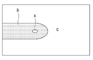
도 3은 종래 터치 패널 인 셀 방식의 액정표시장치에서 터치된 부분을 센싱한 일 결과를 보여준다. 도 3에서 "A" 는 손가락에 의한 터치 지점을, "B" 는 손가락에 의해 외부광이 차단되는 부분을, "C" 는 외부광에 노출되는 부분을 각각 나타낸다. 여기서, "A" 는 터치로 인한 백라이트 광의 반사에 의해 "B" 보다 밝은 데이터값을 갖는다.FIG. 3 shows a result of sensing a touched portion in a conventional liquid crystal display of a touch panel. In Fig. 3, "A" represents a touch point by a finger, "B" represents a portion where external light is blocked by a finger, and "C" Here, "A" has a data value brighter than "B " due to the reflection of the backlight due to the touch.
그런데, 이러한 터치 패널 인 셀 방식의 액정표시장치는 터치 된 부분을 추출하기 위해 "A" 외에 "C" 까지 모두 알고리즘에 적용하기 때문에 터치 인식 알고리즘의 복잡화를 초래한다. 또한, 이러한 터치 패널 인 셀 방식의 액정표시장치는 터치 된 부분을 추출하기 위해 "A" 외에 "C" 까지 모두 알고리즘에 적용하기 때문에 "A" 와 "C" 의 데이터값이 유사한 경우 즉, "A" 와 "C" 의 밝기가 유사한 경우 터치 인식의 신뢰성이 저하된다는 문제점이 있다. However, such a cell-type liquid crystal display device that is a touch panel is complicated in the touch recognition algorithm because it applies all of "A" to "C" to the algorithm in order to extract the touched portion. In order to extract the touched portion, the cell type liquid crystal display device such as this touch panel applies all of "A" to "C" to the algorithm. Therefore, when the data values of "A" and "C" A "and" C "are similar to each other, the reliability of the touch recognition deteriorates.
따라서, 본 발명의 목적은 터치 인식의 알고리즘을 단순화함과 아울러 터치 인식의 신뢰성을 높이도록 한 액정표시장치를 제공하는 데 있다.Accordingly, it is an object of the present invention to provide a liquid crystal display device which simplifies the algorithm of touch recognition and improves the reliability of touch recognition.
상기 목적을 달성하기 위하여, 본 발명의 일 실시예에 따른 액정표시장치는 게이트라인들과 데이터라인들의 교차 영역마다 화소 회로와 터치 여부에 따라 광전류를 다르게 발생하는 터치 센서 회로를 포함하는 다수의 화소들을 가지며, 제1 기간 동안 노멀 데이터(RGB)를 표시하고 상기 제1 기간에 이은 제2 기간 동안 블랙 데이터(BD)를 표시하는 액정표시패널; 상기 제1 기간 및 상기 제2 기간 동안 상기 액정표시패널의 배면에 광을 조사하기 위한 백라이트 유닛; 상기 터치 센서 회로로부터의 광전류를 광감지 데이터로 변환하는 리드아웃 집적회로; 하나의 메모리를 포함하고, 상기 제1 기간 동안 상기 리드아웃 집적회로로부터 공급되는 광감지 데이터를 상기 메모리에 저장한 후, 상기 메모리에 저장된 광감지 데이터와 상기 제2 기간 동안 상기 리드아웃 집적회로로부터 공급되는 광감지 데이터 간의 차값을 추출하여 외부광의 영향이 배제된 터치 위치정보를 발생하는 터치 위치정보 검출회로; 및 상기 터치 위치정보를 터치 인식 알고리즘에 적용하여 터치 인식을 위한 프로세서 과정을 수행하는 시스템을 구비하고; 상기 메모리는 상기 제1 기간 동안 상기 리드아웃 집적회로로부터 공급되는 광감지 데이터만을 저장하고, 상기 제2 기간 동안 상기 리드아웃 집적회로로부터 공급되는 광감지 데이터는 저장하지 않는다.According to an aspect of the present invention, there is provided a liquid crystal display device including a plurality of pixels including a pixel circuit and a touch sensor circuit for generating a photocurrent differently depending on whether a pixel circuit is touched at intersecting areas of gate lines and data lines, A liquid crystal display panel displaying normal data (RGB) during a first period and displaying black data (BD) during a second period subsequent to the first period; A backlight unit for irradiating light to the back surface of the liquid crystal display panel during the first period and the second period; A lead-out integrated circuit for converting the photocurrent from the touch sensor circuit into light sensing data; Wherein the photo sense data stored in the memory is stored in the memory after storing the photo sense data supplied from the lead-out integrated circuit during the first period and from the lead-out integrated circuit during the second period, A touch position information detection circuit for extracting a difference value between supplied light sensing data and generating touch position information excluding the influence of external light; And a system for performing a processor process for touch recognition by applying the touch position information to a touch recognition algorithm; The memory stores only the photo sensed data supplied from the lead-out integrated circuit during the first period, and does not store the photo sensed data supplied from the lead-out integrated circuit during the second period.
삭제delete
삭제delete
삭제delete
삭제delete
삭제delete
삭제delete
삭제delete
삭제delete
본 발명에 따른 액정표시장치 및 그 구동방법은 터치 인식의 알고리즘을 단순화할 수 있음과 아울러 터치 인식의 신뢰성을 크게 높일 수 있다.The liquid crystal display device and the driving method thereof according to the present invention can simplify the algorithm of touch recognition and greatly improve the reliability of the touch recognition.
이하, 본 발명의 바람직한 실시 예를 도 4 내지 도 12를 참조하여 상세하게 설명하기로 한다. Hereinafter, a preferred embodiment of the present invention will be described in detail with reference to FIGS. 4 to 12. FIG.
도 4는 본 발명의 일 실시예에 따른 액정표시장치를 나타내는 블럭도이다.4 is a block diagram illustrating a liquid crystal display device according to an embodiment of the present invention.
도 4를 참조하면, 본 발명의 일 실시예에 따른 액정표시장치는 다수의 게이트라인들(G0 내지 Gn)과 다수의 데이터라인들(D1 내지 Dm) 및 다수의 구동전압 공급라인들(VL1 내지 VLn)이 교차되고 그 교차부에 터치 센서 회로를 갖는 화소(P)들이 배치되며 블랙 데이터(BD) 삽입 방식에 의해 임펄스 구동되는 액정표시패널(10) 과, 데이터라인들(D1 내지 Dm)에 데이터전압을 공급하기 위한 데이터 구동회로(20)와, 게이트라인들(G1 내지 Gn)에 스캔펄스를 공급하기 위한 게이트 구동회로(30)와, 데이터 구동회로(20) 및 게이트 구동회로(30)의 구동 타이밍을 제어하기 위한 타이밍 콘트롤러(40)와, 터치 센서 회로의 구동에 필요한 구동전압을 구동전압 공급라인들(VL1 내지 VLn)에 공급하는 구동전압 공급회로(50)와, 액정표시패널(10)의 배면에 광을 조사하기 위한 백라이트 유닛(60)과, 터치 센서 회로로부터의 광전류를 광감지 데이터(LSdata)로 변환하는 리드아웃 집적회로(70)와, 임펄스 구동을 위해 타이밍 콘트롤러(40)로부터 발생되는 제1 및 제2 게이트 스타트 펄스(GSP1,GSP2)와 리드아웃 집적회로(70)로부터의 광감지 데이터(LSdata)를 이용하여 외부광의 영향이 배제된 터치 위치정보(XY)를 발생하는 터치 위치정보 검출회로 (80)와, 터치 위치정보(XY)를 터치 인식 알고리즘에 적용하여 터치 인식을 위한 프로세서 과정을 수행하는 시스템(90)을 구비한다.4, a liquid crystal display according to an exemplary embodiment of the present invention includes a plurality of gate lines G0 to Gn, a plurality of data lines D1 to Dm, and a plurality of driving voltage supply lines VL1 to VL1, A liquid
액정표시패널(10)은 컬러필터를 포함하는 상부기판과, 화소 회로 및 터치 센서 회로를 포함하는 화소(P)들이 형성되는 하부기판과, 상부기판과 하부기판 사이에 협지되는 액정층을 구비한다. The liquid
이 액정표시패널(10)의 하부기판 상에는 다수의 데이터라인들(D1 내지 Dm)과 다수의 게이트라인들(G0 내지 Gn)이 직교되고 또한, 게이트라인들(G0 내지 Gn)과 평행한 다수의 구동전압 공급라인들(VL1 내지 VLn), 게이트라인들(G0 내지 Gn)과 구동전압 공급라인들(VL1 내지 VLn)과 직교되는 다수의 리드아웃라인들(ROL1 내지 ROLm)이 형성된다. 데이터라인들(D1 내지 Dm)과 게이트라인들(G1 내지 Gn)의 교차 부에는 도 8과 같은 화소 TFT(TFT1), 액정셀들(Clc) 및 스토리지 커패시터(Cst1)를 포함하는 화소 회로(P1)가 형성되고, 구동전압 공급라인들(VL1 내지 VLn)과 리드아웃라인들(ROL1 내지 ROLm)의 교차부에는 도 8과 같은 센서 TFT(S-TFT), 센서 커패시터(Cst2) 및 스위치 TFT(TFT2)를 포함하는 터치 센서 회로(P2)가 형성된다. 구동전압 공급라인들(VL1 내지 VLn) 각각은 터치 센서 회로(P2)에 고전위 구동전압을 공급하기 위한 공급라인과, 터치 센서 회로(P2)에 바이어스 전압을 공급하기 위한 공급라인을 포함한다. 터치 센서 회로(P2)는 손가락 등과 같은 불투명 물체(이하 "손가락" 이라 함)의 터치 여부에 따라 광전류를 다르게 발생하고, 이 광전류를 리드아웃라인들(ROL1 내지 ROLm)을 통해 리드아웃 집적회로(70)로 공급한다. A plurality of data lines D1 to Dm and a plurality of gate lines G0 to Gn are orthogonal to one another and a plurality of gate lines G0 to Gn parallel to the gate lines G0 to Gn are formed on a lower substrate of the liquid
액정표시패널(10)의 상부기판 상에는 화소(P)들 간 경계부를 가려주기 위한 블랙 매트릭스가 형성된다. 액정층을 사이에 두고 화소전극과 대향하여 공통전압이 공급되는 공통전극은 TN(Twisted Nematc) 모드 및 VA(Vertical Alignment) 모드와 같은 수직 전계 모드에서는 상부기판에 형성되고, IPS(In Plane Switching) 모드와 FFS(Fringe Field Switching) 모드와 같은 수평 전계 모드에서는 하부기판 상에 형성된다. On the upper substrate of the liquid
데이터 구동회로(20)는 타이밍 콘트롤러(40)로부터의 데이터 제어신호(DDC)에 응답하여 노멀 데이터(RGB)와 블랙 데이터(BD)를 감마기준전압 발생부(미도시)로부터의 감마기준전압들(GMA)을 기반하여 아날로그 감마보상전압으로 변환하고, 그 아날로그 감마보상전압을 데이터전압으로써 액정표시패널(10)의 데이터라인들(D1 내지 Dm)에 공급한다. The
게이트 구동회로(30)는 타이밍 콘트롤러(40)로부터의 게이트 제어신호(GDC)에 응답하여 스캔펄스를 발생하고 그 스캔펄스를 게이트라인들(G1 내지 Gn)에 순차적으로 공급하여 데이터전압이 공급되는 액정표시패널(10)의 수평라인을 선택한다.The
타이밍 콘트롤러(40)는 임펄스 구동을 위한 블랙 데이터(BD)를 생성하고, 이 블랙 데이터(BD)와 시스템(90)으로부터의 노멀 데이터(RGB)를 액정표시패널(10)에 맞게 재정렬하여 데이터 구동회로(20)에 공급한다. 그리고, 타이밍 콘트롤러(40)는 시스템(90)으로부터의 타이밍 제어신호들(Vsync, Hsync, DCLK, DE)을 이용하여 데이터 구동회로(20)를 제어하기 위한 데이터 제어신호(DDC)와, 게이트 구동회로(30)를 제어하기 위한 게이트 제어신호(GDC)를 생성한다. The
데이터 제어신호(DDC)는 라이징(Rising) 또는 폴링(Falling) 에지에 기준하여 데이터 구동회로(20) 내에서 데이터의 래치동작을 지시하는 소스 샘플링 클럭(Source Sampling Clock : SSC), 데이터 구동회로(20)의 출력을 지시하는 소스 출력 인에이블신호(SOE), 및 액정표시패널(10)의 액정셀들(Clc)에 공급될 데이터전압의 극성을 지시하는 극성제어신호(POL) 등을 포함한다. The data control signal DDC includes a source sampling clock (SSC) for instructing a latch operation of data in the
게이트 제어신호(GDC)는 한 화면이 표시되는 1 프레임기간 중에서 스캔이 시작되는 시작 수평라인을 지시하는 게이트 스타트 펄스(Gate Start Pulse : GSP), 게이트 구동회로(30) 내의 쉬프트 레지스터에 입력되어 게이트 스타트 펄스(GSP)를 순차적으로 쉬프트시키기 위한 타이밍 제어신호로써 화소 TFT의 온(ON) 기간에 대응하는 펄스폭으로 발생되는 게이트 쉬프트 클럭신호(Gate Shift Clock : GSC), 및 게이트 구동회로(30)의 출력을 지시하는 게이트 출력 인에이블신호(Gate Output Enable : GOE) 등을 포함한다. 여기서, 게이트 스타트 펄스(GSP)는 도 5에 도시된 바와 같이, 1 프레임기간 중에서 노멀 데이터(RGB)의 스캔 시작 수평라인을 지시하는 제1 게이트 스타트 펄스(GSP1)와, 블랙 데이터(BD)의 스캔 시작 수평라인을 지시하는 제2 게이트 스타트 펄스(GSP2)를 포함한다.The gate control signal GDC is input to a shift register in the
구동전압 공급회로(50)는 터치 센서 회로(P2)의 구동에 필요한 고전위 구동전압과 바이어스 전압을 발생하여 구동전압 공급라인들(VL1 내지 VLn)에 공급한다.The driving
백라이트 유닛(60)은 액정표시패널(10)의 배면에서 액정표시패널(116)과 중첩되게 설치되는 다수의 램프들을 구비한다. 백라이트 유닛(60)에 사용되는 램프는 냉음극형광램프(Cold Cathode Fluorescent Lamp; CCFL), 외부전극형광램프(External Electrode Fluorescent Lamp; EEFL), 열음극형광램프(Heat Cathode Fluorescent Lamp; HCFL) 중 어느 하나일 수 있다. 램프들은 인버터(미도시)의 구동에 의해 액정표시패널(10)의 배면에 광을 조사한다. 한편, 백라이트 유닛(60)은 램프들 대신에 또는 램프들과 함께 다수의 발광다이오드들을 구비할 수도 있다.The
리드아웃 집적회로(70)는 액정표시패널(10)의 리드아웃라인들(ROL1 내지 RLOm)에 각각 접속되는 다수의 회로들을 포함하며, 리드아웃라인들(ROL1 내지 RLOm)로부터의 광전류를 디지털 신호인 광감지 데이터(LSdata)로 변환하여 터치 위치정보 검출회로(80)에 공급한다. The lead-out integrated
터치 위치정보 검출회로(80)는 임펄스 구동을 위해 타이밍 콘트롤러(40)로부터 발생되는 제1 및 제2 게이트 스타트 펄스(GSP1,GSP2)와 리드아웃 집적회로(70)로부터의 광감지 데이터(LSdata)를 이용하여 외부광의 영향이 배제된 터치 위치정 보(XY)를 발생한다. 이를 위해, 터치 위치정보 검출회로(80)는 도 6에 도시된 바와 같이, RGB 스캔 저장부(82), BD 스캔 저장부(84), 및 차값 추출부(86)를 구비한다.The touch position
RGB 스캔 저장부(82)는 도 5와 같은 제1 게이트 스타트 펄스(GSP1)에 동기되는 제1 기간(T1) 동안, 리드아웃 집적회로(70)로부터 공급되는 광감지 데이터(LSdata)를 저장한다. 이러한 RGB 스캔 저장부(82)에 저장된 정보는 도 7a와 같다. 도 7a에서, "A" 는 손가락에 의한 터치 지점에 대한 정보를, "B" 는 손가락에 의해 외부광이 차단되는 부분에 대한 정보를, "C" 는 외부광에 노출되는 부분에 대한 정보를 각각 나타낸다.The RGB
BD 스캔 저장부(84)는 도 5와 같은 제2 게이트 스타트 펄스(GSP2)에 동기되는 제2 기간(T2) 동안, 리드아웃 집적회로(70)로부터 공급되는 광감지 데이터(LSdata)를 저장한다. 이러한 BD 스캔 저장부(84)에 저장된 정보는 도 7b와 같다. 도 7b에서, "B" 는 손가락에 의해 외부광이 차단되는 부분에 대한 정보를, "C" 는 외부광에 노출되는 부분에 대한 정보를 각각 나타낸다.The BD
차값 추출부(86)는 RGB 스캔 저장부(82) 및 BD 스캔 저장부(84)로부터의 광감지 데이터들을 일대일로 비교하고, 그 결과 비교된 데이터들의 차값을 추출함으로써 외부광의 영향이 배제된 터치 위치정보(XY)를 발생한다. 이 추출된 차값 정보는 도 7c에 도시된 바와 같이 손가락에 의한 터치 지점에 대한 정보(A) 만을 포함한다.The difference
한편, 터치 위치정보 검출회로(80)에서는 메모리 수 절감에 대응하기 위해 두 개의 메모리(82,84)가 하나의 메모리에 통합될 수도 있다. 이 통합된 메모리를 이용하여, 터치 위치정보 검출회로(80)는 먼저 제1 기간(T1) 동안 리드아웃 집적회로(70)로부터 공급되는 광감지 데이터(LSdata)를 저장한 후, 이 저장된 광감지 데이터(LSdata)로부터 제2 기간(T2) 동안 리드아웃 집적회로(70)로부터 공급되는 광감지 데이터(LSdata)를 감산하고, 이 차값을 제1 기간(T1) 동안 저장된 광감지 데이터(LSdata)에 오버 라이트(Overwrite) 할 수 있다.On the other hand, in the touch position
시스템(90)은 인터페이스회로(미도시)를 통해 공급되는 외부로부터의 아날로그 영상 데이터를 디지털 노멀 데이터(RGB)로 변환하여 타이밍 콘트롤러(40)에 공급한다. 시스템(90)은 인터페이스회로로부터의 영상 데이터를 이용하여 복합 영상신호를 추출하고, 추출된 복합 영상신호를 이용하여 액정표시패널(10)의 해상도에 맞는 동기신호(H.V sync), 데이터 인에이블 신호(DE) 및 도트 클럭(DCLK)을 생성하여 타이밍 콘트롤러(40)에 공급한다. The
특히, 시스템(90)은 터치 알고리즘 처리부(92)를 포함하여 터치 위치정보 검출회로(80)로부터 공급되는 터치 위치정보(XY)를 터치 인식 알고리즘에 적용함으로써, 터치 인식을 위한 프로세서 과정을 수행하며 그 수행 결과를 다시 액정표시패널(10)에 반영한다. 상술했듯이, 터치 위치정보(XY)에는 손가락에 의한 터치 지점에 대한 정보만이 포함되어 있으므로, 터치 알고리즘 처리부(92)에 내장된 터치 인식 알고리즘이 종래에 비해 크게 간소화될 수 있다. 또한, 터치 위치정보(XY)에는 손가락에 의한 터치 지점에 대한 정보만이 포함되어 있으므로, 터치 인식의 신뢰성 크게 향상될 수 있다.In particular, the
도 8은 도 4에 도시된 화소(P)의 등가 회로도이다.8 is an equivalent circuit diagram of the pixel P shown in Fig.
도 8을 참조하면, 화소(P)는 j 번째 게이트라인(Gj)과 j 번째 데이터라인(Dj)의 교차부에 형성되는 화소 회로(P1)와, j 번째 제1 공급라인(VLja) 및 j 번째 제2 공급라인(VLjb)과 j 번째 리드아웃라인(ROLj)의 교차부에 형성되는 터치 센서 회로(P2)를 구비한다.8, a pixel P includes a pixel circuit P1 formed at an intersection of a j-th gate line Gj and a j-th data line Dj, a j-th first supply line VLja, and j And a touch sensor circuit P2 formed at the intersection of the second supply line VLjb and the j-th lead-out line ROLj.
화소 회로(P1)는 액정셀(Clc)과, 게이트라인(Gj)과 데이터라인(Dj)의 교차 영역에 형성되어 액정셀(Clc)을 구동하기 위한 화소 TFT(TFT1)와, 액정셀(Clc)의 충전전압을 한 프레임 동안 유지시키기 위한 스토리지 커패시터(Cst1)를 구비한다. The pixel circuit P1 includes a liquid crystal cell Clc and a pixel TFT TFT1 formed in a crossing region of the gate line Gj and the data line Dj for driving the liquid crystal cell Clc, And a storage capacitor Cst1 for maintaining the charging voltage of the storage capacitor Cst1 for one frame.
화소 TFT(TFT1)는 게이트라인(GLj)으로부터의 스캔펄스에 응답하여 데이터라인(DLj)을 통해 공급되는 데이터전압을 액정셀(Clc)의 화소전극에 공급한다. 이를 위하여 화소 TFT(TFT1)의 게이트전극은 게이트라인(GLj)에 접속되고, 소스전극은 데이터라인(DLj)에 접속되며, 드레인전극은 액정셀(Clc)의 화소전극에 접속된다. 액정셀(Clc)은 데이터전압과 공통전압(Vcom)의 전위차로 충전되며, 이 전위차로 형성되는 전계에 의해 액정분자들의 배열이 바뀌면서 투과되는 빛의 광량을 조절하거나 빛을 차단하게 된다. 스토리지 커패시터(Cst1)는 화소 TFT(TFT1)의 드레인전극과 제2 공급라인(VLjb) 사이에 접속된다.The pixel TFT TFT1 supplies a data voltage supplied through the data line DLj to the pixel electrode of the liquid crystal cell Clc in response to a scan pulse from the gate line GLj. To this end, the gate electrode of the pixel TFT (TFT1) is connected to the gate line GLj, the source electrode thereof is connected to the data line DLj, and the drain electrode thereof is connected to the pixel electrode of the liquid crystal cell Clc. The liquid crystal cell Clc is charged with the potential difference between the data voltage and the common voltage Vcom, and the arrangement of the liquid crystal molecules is changed by the electric field formed by this potential difference to adjust the light amount of the transmitted light or block the light. The storage capacitor Cst1 is connected between the drain electrode of the pixel TFT (TFT1) and the second supply line (VLjb).
터치 센서 회로(P2)는 구동전압이 공급되는 기간 동안 터치 지점에 대응되는지 여부에 따라 광전류(i)를 다르게 발생하는 센서 TFT(S-TFT)와, 광전류(i)에 의한 전하들을 저장하는 센서 커패시터(Cst2), 및 센서 커패시터(Cst2)에 저장되어 있는 전하들을 리드아웃라인(ROLj)으로 스위칭하는 스위치 TFT(TFT2)를 구비한다. The touch sensor circuit P2 includes a sensor TFT (S-TFT) that generates a photocurrent i differently depending on whether or not the touch point corresponds to a period during which the driving voltage is supplied, a sensor And a switch TFT (TFT2) for switching the charges stored in the capacitor Cst2 and the sensor capacitor Cst2 to the lead-out line ROLj.
센서 TFT(S-TFT)의 게이트전극은 제2 공급라인(VLjb)에 접속되고, 소스전극은 제1 공급라인(VLja)에 접속되며, 드레인전극은 제1 노드(N1)에 접속된다. 센서 TFT(S-TFT)의 게이트전극에는 자신의 문턱전압 이하의 전압으로 설정된 바이어스전압(Vbias)이 공급되고, 센서 TFT(S-TFT)의 소스전극에는 구동전압이 공급된다. 이러한 센서 TFT(S-TFT)는 화소 TFT(TFT1) 및 스위치 TFT(TFT2)와는 달리 상부기판의 블랙 매트릭스에 의해 가려지지 않기 때문에 외부로부터 입사되는 광에 반응하여 구동전압이 공급되는 기간 동안 광전류(i)를 발생하되, 터치 지점 여부에 따라 다른 크기의 광전류(i)를 발생한다. 다시 말해, 센서 TFT(S-TFT)는 백라이트보다 어두운 조도 환경(실내 환경)에서는 터치 지점에 대응되지 않을 때에 비해 터치 지점에 대응될 때에 큰 광전류(i)를 발생하는 반면, 백라이트보다 밝은 조도 환경(실외 환경)에서는 터치 지점에 대응되지 않을 때에 비해 터치 지점에 대응될 때에 작은 광전류(i)를 발생한다.The gate electrode of the sensor TFT (S-TFT) is connected to the second supply line (VLjb), the source electrode is connected to the first supply line (VLja), and the drain electrode is connected to the first node (N1). A bias voltage Vbias set at a voltage equal to or lower than the threshold voltage of the sensor TFT (S-TFT) is supplied to the gate electrode of the sensor TFT (S-TFT), and a driving voltage is supplied to the source electrode of the sensor TFT (S-TFT). Since the sensor TFT (S-TFT) is not covered by the black matrix of the upper substrate, unlike the pixel TFT (TFT1) and the switch TFT (TFT2), the photoelectric current i), but generates a photocurrent (i) of different magnitude depending on whether or not the touch point is present. In other words, the sensor TFT (S-TFT) generates a large photocurrent (i) when it corresponds to the touch point, compared with when it does not correspond to the touch point in a dark illumination environment (indoor environment) (I) is generated when the touch point is not corresponded to the touch point in the case of the touch point (outdoor environment).
광전류(i)에 의한 전하들은 제1 노드(N1)와 제2 공급라인(VLjb) 사이에 접속된 센서 커패시터(Cst2)에 저장된다. 제1 노드의 전압(VN1)은 센서 커패시터(Cst2)에 저장되는 전하들에 의해, 스위치 TFT(TFT2)가 턴 온 될 때까지 점점 증가하게 된다. 제1 노드의 전압(VN1)은 구동전압이 공급되는 기간 동안 터치 지점에 대응되는지 여부에 따라 다른 크기를 갖는다. 다시 말해, 제1 노드의 전압(VN1)은 백라이트보다 어두운 조도 환경(실내 환경)에서는 터치 지점에 대응되지 않을 때에 비해 터치 지점에 대응될 때가 더 큰 값을 갖고, 백라이트보다 밝은 조도 환경(실외 환경)에서는 터치 지점에 대응되지 않을 때에 비해 터치 지점에 대응 될 때가 더 작은 값을 갖는다. Charges by the photocurrent i are stored in the sensor capacitor Cst2 connected between the first node N1 and the second supply line VLjb. The voltage VN1 of the first node is gradually increased by the charges stored in the sensor capacitor Cst2 until the switch TFT TFT2 is turned on. The voltage VN1 at the first node has different magnitudes depending on whether or not the voltage corresponds to the touch point during the period in which the drive voltage is supplied. In other words, the voltage VN1 of the first node has a larger value when it corresponds to the touch point than when it does not correspond to the touch point in a dark illumination environment (indoor environment) than the backlight, ) Has a smaller value when corresponding to the touch point than when it is not corresponding to the touch point.
스위치 TFT(TFT2)의 게이트전극은 j-1 번째 게이트라인(Gj-1)에 접속되고, 소스전극은 제1 노드(N1)에 접속되며, 드레인전극은 리드아웃라인(ROLj)에 접속된다. 스위치 TFT(TFT2)는 j-1 번째 게이트라인(Gj-1)에 공급되는 스캔펄스(SPj-1)에 응답하여 턴 온 됨으로써 제1 노드전압(VN1)을 광감지신호로써 리드아웃라인(ROLj)으로 출력한다.The gate electrode of the switch TFT TFT2 is connected to the (j-1) th gate line Gj-1, the source electrode thereof is connected to the first node N1, and the drain electrode thereof is connected to the lead-out line ROLj. The switch TFT TFT2 is turned on in response to the scan pulse SPj-1 supplied to the (j-1) th gate line Gj-1 to output the first node voltage VNl as the photo- .
도 9는 본 발명의 다른 실시예에 따른 액정표시장치를 나타내는 블럭도이다.9 is a block diagram illustrating a liquid crystal display device according to another embodiment of the present invention.
도 9를 참조하면, 본 발명의 다른 실시예에 따른 액정표시장치는 다수의 게이트라인들(G0 내지 Gn)과 다수의 데이터라인들(D1 내지 Dm) 및 다수의 구동전압 공급라인들(VL1 내지 VLn)이 교차되고 그 교차부에 터치 센서 회로를 갖는 화소(P)들이 배치되는 액정표시패널(110)과, 데이터라인들(D1 내지 Dm)에 데이터전압을 공급하기 위한 데이터 구동회로(120)와, 게이트라인들(G1 내지 Gn)에 스캔펄스를 공급하기 위한 게이트 구동회로(130)와, 데이터 구동회로(120) 및 게이트 구동회로(130)의 구동 타이밍을 제어하기 위한 타이밍 콘트롤러(140)와, 터치 센서 회로의 구동에 필요한 구동전압을 구동전압 공급라인들(VL1 내지 VLn)에 공급하는 구동전압 공급회로(150)와, 액정표시패널(110)의 배면에 순차적으로 점멸하는 광을 조사하기 위한 백라이트 유닛(160)과, 터치 센서 회로로부터의 광전류를 광감지 데이터(LSdata)로 변환하는 리드아웃 집적회로(170)와, 임펄스 구동을 위해 타이밍 콘트롤러(140)로부터 백라이트 제어신호(SBL)와 리드아웃 집적회로(170)로부터의 광감지 데이터(LSdata)를 이용하여 외부광의 영향이 배제된 터치 위치정보(XY)를 발 생하는 터치 위치정보 검출회로(180)와, 터치 위치정보(XY)를 터치 인식 알고리즘에 적용하여 터치 인식을 위한 프로세서 과정을 수행하는 시스템(190)을 구비한다.9, a liquid crystal display according to another embodiment of the present invention includes a plurality of gate lines G0 to Gn, a plurality of data lines D1 to Dm, and a plurality of driving voltage supply lines VL1 to VL1, A data driving circuit 120 for supplying a data voltage to the data lines D1 to Dm; a liquid crystal display panel 110 in which pixels P having a touch sensor circuit are arranged at intersections of the pixels P, A gate driving circuit 130 for supplying a scan pulse to the gate lines G1 to Gn and a timing controller 140 for controlling the driving timing of the data driving circuit 120 and the gate driving circuit 130, A driving voltage supply circuit 150 for supplying a driving voltage required for driving the touch sensor circuit to the driving voltage supply lines VL1 to VLn and a driving circuit for applying light to the back surface of the liquid crystal display panel 110 A backlight unit 160 for driving the touch sensor circuit 160, Out integrated circuit 170 for converting the photocurrent from the lead-out integrated circuit 170 to the photodetection data LSdata from the timing controller 140 for impulse driving, A touch position information detection circuit 180 which generates touch position information XY in which the influence of external light is eliminated by using data LSdata and a touch position information detection circuit 180 which applies touch position information XY to the touch recognition algorithm, And a system 190 for performing a processor process.
액정표시패널(110) 및 구동전압 공급회로(150)는 도 4에 도시된 액정표시패널(10) 및 구동전압 공급회로(50)와 각각 실질적으로 동일하므로 이들에 대한 상세한 설명은 생략하기로 한다.The liquid
데이터 구동회로(120)는 타이밍 콘트롤러(140)로부터의 데이터 제어신호(DDC)에 응답하여 디지털 비디오 데이터(RGB)를 감마기준전압 발생부(미도시)로부터의 감마기준전압들(GMA)을 기반하여 아날로그 감마보상전압으로 변환하고, 그 아날로그 감마보상전압을 데이터전압으로써 액정표시패널(110)의 데이터라인들(D1 내지 Dm)에 공급한다. The
게이트 구동회로(130)는 타이밍 콘트롤러(140)로부터의 게이트 제어신호(GDC)에 응답하여 스캔펄스를 발생하고 그 스캔펄스를 게이트라인들(G1 내지 Gn)에 순차적으로 공급하여 데이터전압이 공급되는 액정표시패널(110)의 수평라인을 선택한다.The
타이밍 콘트롤러(140)는 시스템(190)으로부터 입력되는 디지털 비디오 데이터(RGB)를 액정표시패널(110)에 맞게 재정렬하여 데이터 구동회로(120)에 공급한다. 그리고, 타이밍 콘트롤러(140)는 시스템(190)으로부터의 타이밍 제어신호들(Vsync, Hsync, DCLK, DE)을 이용하여 데이터 구동회로(120)를 제어하기 위한 데이터 제어신호(DDC)와, 게이트 구동회로(130)를 제어하기 위한 게이트 제어신호(GDC)와, 백라이트를 제어하기 위한 백라이트 제어신호(SBL)를 생성한다. The
데이터 제어신호(DDC)는 라이징(Rising) 또는 폴링(Falling) 에지에 기준하여 데이터 구동회로(120) 내에서 데이터의 래치동작을 지시하는 소스 샘플링 클럭(Source Sampling Clock : SSC), 데이터 구동회로(120)의 출력을 지시하는 소스 출력 인에이블신호(SOE), 및 액정표시패널(110)의 액정셀들(Clc)에 공급될 데이터전압의 극성을 지시하는 극성제어신호(POL) 등을 포함한다. The data control signal DDC includes a source sampling clock (SSC) for instructing a latch operation of data in the
게이트 제어신호(GDC)는 한 화면이 표시되는 1 프레임기간 중에서 스캔이 시작되는 시작 수평라인을 지시하는 게이트 스타트 펄스(Gate Start Pulse : GSP), 게이트 구동회로(130) 내의 쉬프트 레지스터에 입력되어 게이트 스타트 펄스(GSP)를 순차적으로 쉬프트시키기 위한 타이밍 제어신호로써 화소 TFT의 온(ON) 기간에 대응하는 펄스폭으로 발생되는 게이트 쉬프트 클럭신호(Gate Shift Clock : GSC), 및 게이트 구동회로(130)의 출력을 지시하는 게이트 출력 인에이블신호(Gate Output Enable : GOE) 등을 포함한다. The gate control signal GDC is input to a shift register in the
백라이트 제어신호(SBL)는 도 10 및 도 11과 같이 다수의 램프들(L1 내지 Lk)에 대응되는 다수의 제어신호들(SBL1 내지 SBLk)을 포함한다. 제어신호들(SBL1 내지 SBLk) 각각은 램프가 점등되는 제1 기간(T1)에 대응하여 하이 논리 레벨로 발생되는 점등 제어신호(BLon)와, 램프가 소등되는 제2 기간(T2)에 대응하여 로우 논리 레벨로 발생되는 소등 제어신호(BLoff)를 포함한다. 이러한 제어신호들(SBL1 내지 SBLk)은 일정한 위상 쉬프트 값을 가지고 순차적으로 발생된 후 램프들(L1 내지 Lk)에 일대일로 접속된 다수의 인버터(I1 내지 Ik)에 공급됨으로써 임펄스 구동을 구현한다.The backlight control signal SBL includes a plurality of control signals SBL1 to SBLk corresponding to the plurality of lamps L1 to Lk as shown in Figs. Each of the control signals SBL1 to SBLk corresponds to a lighting control signal BLon generated at a high logic level corresponding to a first period T1 in which the lamp is lit and a second period T2 during which the lamp is turned off And a light-off control signal BLoff generated at a low logic level. These control signals SBL1 to SBLk are sequentially generated with a predetermined phase shift value and then supplied to a plurality of inverters I1 to Ik connected in a one-to-one manner to the ramps L1 to Lk to implement impulse driving.
백라이트 유닛(160)은 액정표시패널(110)의 배면에서 액정표시패널(116)과 중첩되게 설치되는 다수의 램프들을 구비한다. 백라이트 유닛(160)에 사용되는 램프는 냉음극형광램프(Cold Cathode Fluorescent; CCFL), 외부전극형광램프(External Electrode Flouscent; EEFL), 열음극형광램프(Heat Cathode Fluorescent; HCFL) 중 어느 하나일 수 있다. 램프들은 타이밍 콘트롤러(140)로부터의 백라이트 제어신호(SBL)에 응답하여 순차적으로 점멸되는 광을 액정표시패널(110)의 배면에 조사한다. 한편, 백라이트 유닛(160)은 램프들 대신에 또는 램프들과 함께 다수의 발광다이오드들을 구비할 수도 있다.The
리드아웃 집적회로(170)는 액정표시패널(110)의 리드아웃라인들(ROL1 내지 RLOm)에 각각 접속되는 다수의 회로들을 포함하며, 리드아웃라인들(ROL1 내지 RLOm)로부터의 광전류를 디지털 신호인 광감지 데이터(LSdata)로 변환하여 터치 위치정보 검출회로(180)에 공급한다. The lead-out
터치 위치정보 검출회로(180)는 임펄스 구동을 위해 타이밍 콘트롤러(140)로부터의 백라이트 제어신호(SBL)와 리드아웃 집적회로(170)로부터의 광감지 데이터(LSdata)를 이용하여 외부광의 영향이 배제된 터치 위치정보(XY)를 발생한다. 이를 위해, 터치 위치정보 검출회로(180)는 도 12에 도시된 바와 같이, 점등 스캔 저장부(182), 소등 스캔 저장부(184), 및 차값 추출부(186)를 구비한다.The touch position
점등 스캔 저장부(182)는 도 11과 같은 점등 제어신호(BLon)에 동기되는 제1 기간(T1) 동안, 리드아웃 집적회로(170)로부터 공급되는 광감지 데이터(LSdata)를 저장한다. 이러한 점등 스캔 저장부(182)에 저장된 정보는 도 7a와 같다. 도 7a에서, "A" 는 손가락에 의한 터치 지점에 대한 정보를, "B" 는 손가락에 의해 외부광이 차단되는 부분에 대한 정보를, "C" 는 외부광에 노출되는 부분에 대한 정보를 각각 나타낸다.The lighting
소등 스캔 저장부(184)는 도 11과 같은 소등 제어신호(BLoff)에 동기되는 제2 기간(T2) 동안, 리드아웃 집적회로(170)로부터 공급되는 광감지 데이터(LSdata)를 저장한다. 이러한 소등 스캔 저장부(184)에 저장된 정보는 도 7b와 같다. 도 7b에서, "B" 는 손가락에 의해 외부광이 차단되는 부분에 대한 정보를, "C" 는 외부광에 노출되는 부분에 대한 정보를 각각 나타낸다.The extinction
차값 추출부(186)는 점등 스캔 저장부(182) 및 소등 스캔 저장부(184)로부터의 광감지 데이터들을 일대일로 비교하고, 그 결과 비교된 데이터들의 차값을 추출함으로써 외부광의 영향이 배제된 터치 위치정보(XY)를 발생한다. 이 추출된 차값 정보는 도 7c에 도시된 바와 같이 손가락에 의한 터치 지점에 대한 정보(A) 만을 포함한다.The difference
한편, 터치 위치정보 검출회로(180)에서는 메모리 수 절감에 대응하기 위해 두 개의 메모리(182,184)가 하나의 메모리에 통합될 수도 있다. 이 통합된 메모리를 이용하여, 터치 위치정보 검출회로(180)는 먼저 제1 기간(T1) 동안 리드아웃 집적회로(170)로부터 공급되는 광감지 데이터(LSdata)를 저장한 후, 이 저장된 광감지 데이터(LSdata)로부터 제2 기간(T2) 동안 리드아웃 집적회로(170)로부터 공급되는 광감지 데이터(LSdata)를 감산하고, 이 차값을 제1 기간(T1) 동안 저장된 광감지 데이터(LSdata)에 오버 라이트(Overwrite) 할 수 있다.On the other hand, in the touch position
시스템(190)은 인터페이스회로(미도시)를 통해 공급되는 외부로부터의 아날로그 영상 데이터를 디지털 노멀 데이터(RGB)로 변환하여 타이밍 콘트롤러(140)에 공급한다. 시스템(190)은 인터페이스회로로부터의 영상 데이터를 이용하여 복합 영상신호를 추출하고, 추출된 복합 영상신호를 이용하여 액정표시패널(110)의 해상도에 맞는 동기신호(H.V sync), 데이터 인에이블 신호(DE) 및 도트 클럭(DCLK)을 생성하여 타이밍 콘트롤러(140)에 공급한다. The
특히, 시스템(190)은 터치 알고리즘 처리부(192)를 포함하여 터치 위치정보 검출회로(180)로부터 공급되는 터치 위치정보(XY)를 터치 인식 알고리즘에 적용함으로써, 터치 인식을 위한 프로세서 과정을 수행하며 그 수행 결과를 다시 액정표시패널(110)에 반영한다. 상술했듯이, 터치 위치정보(XY)에는 외부광의 영향이 배제된 손가락에 의한 터치 지점에 대한 정보만이 포함되어 있으므로, 터치 알고리즘 처리부(192)에 내장된 터치 인식 알고리즘이 종래에 비해 크게 간소화될 수 있다. 또한, 터치 위치정보(XY)에는 외부광의 영향이 배제된 손가락에 의한 터치 지점에 대한 정보만이 포함되어 있으므로, 터치 인식의 신뢰성이 크게 향상될 수 있다.In particular, the
상술한 바와 같이, 본 발명에 따른 액정표시장치는 터치 인식의 알고리즘을 단순화할 수 있음과 아울러 터치 인식의 신뢰성을 크게 높일 수 있다.As described above, the liquid crystal display device according to the present invention can simplify the algorithm of touch recognition and can greatly enhance the reliability of the touch recognition.
이상 설명한 내용을 통해 당업자라면 본 발명의 기술사상을 일탈하지 아니하는 범위에서 다양한 변경 및 수정이 가능함을 알 수 있을 것이다. 따라서, 본 발명의 기술적 범위는 명세서의 상세한 설명에 기재된 내용으로 한정되는 것이 아니 라 특허 청구의 범위에 의해 정하여져야만 할 것이다. It will be apparent to those skilled in the art that various modifications and variations can be made in the present invention without departing from the spirit or scope of the invention. Therefore, the technical scope of the present invention should not be limited to the contents described in the detailed description of the specification, but should be defined by the claims.
도 1은 액티브 매트릭스 타입의 액정표시장치의 등가회로도.1 is an equivalent circuit diagram of an active matrix type liquid crystal display device.
도 2는 터치 센서 회로의 동작 설명을 위한 도면.2 is a diagram for explaining an operation of a touch sensor circuit;
도 3은 종래 터치 패널 인 셀 방식의 액정표시장치에서 터치된 부분을 센싱한 일 결과를 보여주는 도면.FIG. 3 is a view showing a result of sensing a touched portion in a conventional liquid crystal display of a touch panel. FIG.
도 4는 본 발명의 일 실시예에 따른 액정표시장치를 나타내는 블럭도.4 is a block diagram illustrating a liquid crystal display device according to an embodiment of the present invention.
도 5는 블랙 데이터 삽입을 통해 임펄스 구동을 구현하기 위한 제1 및 제2 게이트 스타트 펄스의 타이밍도.5 is a timing diagram of first and second gate start pulses for implementing impulse driving through black data insertion.
도 6은 도 4에 도시된 터치 위치정보 검출회로의 세부 구성도.6 is a detailed configuration diagram of the touch position information detection circuit shown in Fig.
도 7a는 도 6의 RGB 스캔 저장부 또는 도 12의 점등 스캔 저장부에 저장된 정보를 보여주는 도면.FIG. 7A is a view showing information stored in the RGB scan storage unit of FIG. 6 or the lighting scan storage unit of FIG. 12;
도 7b는 도 6의 BD 스캔 저장부 또는 도 12의 소등 스캔 저장부에 저장된 정보를 보여주는 도면.FIG. 7B is a view showing information stored in the BD scan storage unit of FIG. 6 or the out-of-scan storage unit of FIG. 12;
도 7c는 도 6 또는 도 12의 차값 추출부에 저장된 정보를 보여주는 도면.FIG. 7C is a diagram showing information stored in the difference value extracting unit of FIG. 6 or FIG.
도 8은 도 4에 도시된 화소의 등가 회로도.8 is an equivalent circuit diagram of the pixel shown in Fig.
도 9는 본 발명의 다른 실시예에 따른 액정표시장치를 나타내는 블럭도.9 is a block diagram showing a liquid crystal display device according to another embodiment of the present invention.
도 10은 도 9의 백라이트 유닛의 세부 구성도.10 is a detailed configuration diagram of the backlight unit of FIG.
도 11은 백라이트 제어신호에 포함되는 다수의 제어신호들의 타이밍도.11 is a timing diagram of a plurality of control signals included in a backlight control signal;
도 12는 도 9에 도시된 터치 위치정보 검출회로의 세부 구성도.Fig. 12 is a detailed configuration diagram of the touch position information detection circuit shown in Fig. 9; Fig.
< 도면의 주요 부분에 대한 부호의 설명 >Description of the Related Art
10,110 : 액정표시패널 20,120 : 데이터 구동회로10, 110: liquid
30,130 : 게이트 구동회로 40,140 : 타이밍 콘트롤러30, 130:
50,150 : 구동전압 공급회로 60,160 : 백라이트 유닛50, 150: driving
70,170 : 리드아웃 집적회로 80,180 : 터치 위치정보 검출회로70, 170: lead-out
82 : RGB 스캔 저장부 84 : BD 스캔 저장부82: RGB scan storage unit 84: BD scan storage unit
86,186 : 차값 추출부 182 : 점등 스캔 저장부86, 186: Difference value extracting unit 182:
184 : 소등 스캔 저장부 90,190 : 시스템184: Extinguishing
92,192 : 터치 알고리즘 처리부92, 192: touch algorithm processing section
Claims (9)
Priority Applications (1)
| Application Number | Priority Date | Filing Date | Title |
|---|---|---|---|
| KR20080042033A KR101495347B1 (en) | 2008-05-06 | 2008-05-06 | Liquid crystal display |
Applications Claiming Priority (1)
| Application Number | Priority Date | Filing Date | Title |
|---|---|---|---|
| KR20080042033A KR101495347B1 (en) | 2008-05-06 | 2008-05-06 | Liquid crystal display |
Publications (2)
| Publication Number | Publication Date |
|---|---|
| KR20090116223A KR20090116223A (en) | 2009-11-11 |
| KR101495347B1 true KR101495347B1 (en) | 2015-02-24 |
Family
ID=41601016
Family Applications (1)
| Application Number | Title | Priority Date | Filing Date |
|---|---|---|---|
| KR20080042033A Expired - Fee Related KR101495347B1 (en) | 2008-05-06 | 2008-05-06 | Liquid crystal display |
Country Status (1)
| Country | Link |
|---|---|
| KR (1) | KR101495347B1 (en) |
Families Citing this family (5)
| Publication number | Priority date | Publication date | Assignee | Title |
|---|---|---|---|---|
| KR101681687B1 (en) * | 2010-08-10 | 2016-12-02 | 삼성디스플레이 주식회사 | Organic light emitting display and driving method thereof |
| KR102023437B1 (en) * | 2012-12-21 | 2019-09-20 | 엘지디스플레이 주식회사 | Liquid crystal display device and driving method thereof |
| CN104035249B (en) * | 2013-03-05 | 2017-01-25 | 钟钢 | Liquid crystal display device integrating touch function and touch position detecting method thereof |
| US10803833B1 (en) * | 2019-11-25 | 2020-10-13 | Himax Technologies Limited | Display systems and integrated source driver circuits |
| CN112214128B (en) | 2020-10-09 | 2022-03-08 | 深圳市华星光电半导体显示技术有限公司 | Touch panel |
Citations (4)
| Publication number | Priority date | Publication date | Assignee | Title |
|---|---|---|---|---|
| KR20050117464A (en) * | 2004-06-10 | 2005-12-14 | 삼성전자주식회사 | Display device and driving method thereof |
| KR20060017750A (en) * | 2003-03-31 | 2006-02-27 | 도시바 마쯔시따 디스플레이 테크놀로지 컴퍼니, 리미티드 | Display device and information terminal device |
| JP2006317682A (en) | 2005-05-12 | 2006-11-24 | Hitachi Displays Ltd | Touch panel integrated display device |
| JP2008033701A (en) | 2006-07-31 | 2008-02-14 | Mitsubishi Motors Corp | Touch panel device |
-
2008
- 2008-05-06 KR KR20080042033A patent/KR101495347B1/en not_active Expired - Fee Related
Patent Citations (4)
| Publication number | Priority date | Publication date | Assignee | Title |
|---|---|---|---|---|
| KR20060017750A (en) * | 2003-03-31 | 2006-02-27 | 도시바 마쯔시따 디스플레이 테크놀로지 컴퍼니, 리미티드 | Display device and information terminal device |
| KR20050117464A (en) * | 2004-06-10 | 2005-12-14 | 삼성전자주식회사 | Display device and driving method thereof |
| JP2006317682A (en) | 2005-05-12 | 2006-11-24 | Hitachi Displays Ltd | Touch panel integrated display device |
| JP2008033701A (en) | 2006-07-31 | 2008-02-14 | Mitsubishi Motors Corp | Touch panel device |
Also Published As
| Publication number | Publication date |
|---|---|
| KR20090116223A (en) | 2009-11-11 |
Similar Documents
| Publication | Publication Date | Title |
|---|---|---|
| KR101319340B1 (en) | Liquid Crystal Display Device | |
| KR101322015B1 (en) | Liquid Crystal Display Device | |
| US9058072B2 (en) | Touch sensing apparatus and driving method thereof | |
| US8466892B2 (en) | Display apparatus and method of driving the same | |
| KR20090113127A (en) | LCD and its driving method | |
| KR102350727B1 (en) | Touch screen display device including fingerprint sensor | |
| KR20090127696A (en) | LCD and its driving method | |
| US8619020B2 (en) | Display apparatus | |
| KR101552988B1 (en) | Driving circuit for liquid crystal display device and method for driving the same | |
| KR20120063772A (en) | Display device having touch screen panel and noise compensation method of thereof | |
| KR20160087467A (en) | Method for driving touch screen panel | |
| KR20100005855A (en) | Liquid crystal display and method for driving the same | |
| KR101495347B1 (en) | Liquid crystal display | |
| KR101481666B1 (en) | Liquid Crystal Display Device and Method for Driving the Same | |
| KR102391616B1 (en) | Gate driver and touch screen integrated display device including the same | |
| KR20120034502A (en) | Flat panel display with a built-in touch sensor and driving method thereof | |
| KR20120097762A (en) | Touch sensor integrated liquid cryctal display device | |
| KR101481660B1 (en) | Liquid crystal display and driving method thereof | |
| JP4788232B2 (en) | Display device and display method | |
| KR101789330B1 (en) | Liquid crystal display panel including photo sensor and display device using the same | |
| KR101548493B1 (en) | Liquid crystal display device | |
| KR20150073781A (en) | Liquid Crystal Display Device | |
| KR101666733B1 (en) | Touch screen integrated display device | |
| KR20150078765A (en) | Display device with integrated touch screen |
Legal Events
| Date | Code | Title | Description |
|---|---|---|---|
| PA0109 | Patent application |
St.27 status event code: A-0-1-A10-A12-nap-PA0109 |
|
| PG1501 | Laying open of application |
St.27 status event code: A-1-1-Q10-Q12-nap-PG1501 |
|
| R18-X000 | Changes to party contact information recorded |
St.27 status event code: A-3-3-R10-R18-oth-X000 |
|
| R18-X000 | Changes to party contact information recorded |
St.27 status event code: A-3-3-R10-R18-oth-X000 |
|
| R18-X000 | Changes to party contact information recorded |
St.27 status event code: A-3-3-R10-R18-oth-X000 |
|
| A201 | Request for examination | ||
| PA0201 | Request for examination |
St.27 status event code: A-1-2-D10-D11-exm-PA0201 |
|
| D13-X000 | Search requested |
St.27 status event code: A-1-2-D10-D13-srh-X000 |
|
| D14-X000 | Search report completed |
St.27 status event code: A-1-2-D10-D14-srh-X000 |
|
| E902 | Notification of reason for refusal | ||
| PE0902 | Notice of grounds for rejection |
St.27 status event code: A-1-2-D10-D21-exm-PE0902 |
|
| AMND | Amendment | ||
| E13-X000 | Pre-grant limitation requested |
St.27 status event code: A-2-3-E10-E13-lim-X000 |
|
| P11-X000 | Amendment of application requested |
St.27 status event code: A-2-2-P10-P11-nap-X000 |
|
| P13-X000 | Application amended |
St.27 status event code: A-2-2-P10-P13-nap-X000 |
|
| E601 | Decision to refuse application | ||
| PE0601 | Decision on rejection of patent |
St.27 status event code: N-2-6-B10-B15-exm-PE0601 |
|
| AMND | Amendment | ||
| E13-X000 | Pre-grant limitation requested |
St.27 status event code: A-2-3-E10-E13-lim-X000 |
|
| J201 | Request for trial against refusal decision | ||
| P11-X000 | Amendment of application requested |
St.27 status event code: A-2-2-P10-P11-nap-X000 |
|
| P13-X000 | Application amended |
St.27 status event code: A-2-2-P10-P13-nap-X000 |
|
| PJ0201 | Trial against decision of rejection |
St.27 status event code: A-3-3-V10-V11-apl-PJ0201 |
|
| PB0901 | Examination by re-examination before a trial |
St.27 status event code: A-6-3-E10-E12-rex-PB0901 |
|
| B701 | Decision to grant | ||
| PB0701 | Decision of registration after re-examination before a trial |
St.27 status event code: A-3-4-F10-F13-rex-PB0701 |
|
| GRNT | Written decision to grant | ||
| PR0701 | Registration of establishment |
St.27 status event code: A-2-4-F10-F11-exm-PR0701 |
|
| PR1002 | Payment of registration fee |
St.27 status event code: A-2-2-U10-U11-oth-PR1002 Fee payment year number: 1 |
|
| PG1601 | Publication of registration |
St.27 status event code: A-4-4-Q10-Q13-nap-PG1601 |
|
| P22-X000 | Classification modified |
St.27 status event code: A-4-4-P10-P22-nap-X000 |
|
| LAPS | Lapse due to unpaid annual fee | ||
| PC1903 | Unpaid annual fee |
St.27 status event code: A-4-4-U10-U13-oth-PC1903 Not in force date: 20180214 Payment event data comment text: Termination Category : DEFAULT_OF_REGISTRATION_FEE |
|
| PC1903 | Unpaid annual fee |
St.27 status event code: N-4-6-H10-H13-oth-PC1903 Ip right cessation event data comment text: Termination Category : DEFAULT_OF_REGISTRATION_FEE Not in force date: 20180214 |