KR101493555B1 - Stereoscopic image display - Google Patents
Stereoscopic image display Download PDFInfo
- Publication number
- KR101493555B1 KR101493555B1 KR20110090874A KR20110090874A KR101493555B1 KR 101493555 B1 KR101493555 B1 KR 101493555B1 KR 20110090874 A KR20110090874 A KR 20110090874A KR 20110090874 A KR20110090874 A KR 20110090874A KR 101493555 B1 KR101493555 B1 KR 101493555B1
- Authority
- KR
- South Korea
- Prior art keywords
- discharge control
- voltage
- gate
- control voltage
- mode
- Prior art date
- Legal status (The legal status is an assumption and is not a legal conclusion. Google has not performed a legal analysis and makes no representation as to the accuracy of the status listed.)
- Expired - Fee Related
Links
Images


Classifications
-
- H—ELECTRICITY
- H04—ELECTRIC COMMUNICATION TECHNIQUE
- H04N—PICTORIAL COMMUNICATION, e.g. TELEVISION
- H04N5/00—Details of television systems
- H04N5/66—Transforming electric information into light information
- H04N5/70—Circuit details for electroluminescent devices
-
- G—PHYSICS
- G09—EDUCATION; CRYPTOGRAPHY; DISPLAY; ADVERTISING; SEALS
- G09G—ARRANGEMENTS OR CIRCUITS FOR CONTROL OF INDICATING DEVICES USING STATIC MEANS TO PRESENT VARIABLE INFORMATION
- G09G3/00—Control arrangements or circuits, of interest only in connection with visual indicators other than cathode-ray tubes
- G09G3/20—Control arrangements or circuits, of interest only in connection with visual indicators other than cathode-ray tubes for presentation of an assembly of a number of characters, e.g. a page, by composing the assembly by combination of individual elements arranged in a matrix no fixed position being assigned to or needed to be assigned to the individual characters or partial characters
- G09G3/34—Control arrangements or circuits, of interest only in connection with visual indicators other than cathode-ray tubes for presentation of an assembly of a number of characters, e.g. a page, by composing the assembly by combination of individual elements arranged in a matrix no fixed position being assigned to or needed to be assigned to the individual characters or partial characters by control of light from an independent source
- G09G3/36—Control arrangements or circuits, of interest only in connection with visual indicators other than cathode-ray tubes for presentation of an assembly of a number of characters, e.g. a page, by composing the assembly by combination of individual elements arranged in a matrix no fixed position being assigned to or needed to be assigned to the individual characters or partial characters by control of light from an independent source using liquid crystals
-
- G—PHYSICS
- G02—OPTICS
- G02B—OPTICAL ELEMENTS, SYSTEMS OR APPARATUS
- G02B30/00—Optical systems or apparatus for producing three-dimensional [3D] effects, e.g. stereoscopic images
-
- G—PHYSICS
- G02—OPTICS
- G02F—OPTICAL DEVICES OR ARRANGEMENTS FOR THE CONTROL OF LIGHT BY MODIFICATION OF THE OPTICAL PROPERTIES OF THE MEDIA OF THE ELEMENTS INVOLVED THEREIN; NON-LINEAR OPTICS; FREQUENCY-CHANGING OF LIGHT; OPTICAL LOGIC ELEMENTS; OPTICAL ANALOGUE/DIGITAL CONVERTERS
- G02F1/00—Devices or arrangements for the control of the intensity, colour, phase, polarisation or direction of light arriving from an independent light source, e.g. switching, gating or modulating; Non-linear optics
- G02F1/01—Devices or arrangements for the control of the intensity, colour, phase, polarisation or direction of light arriving from an independent light source, e.g. switching, gating or modulating; Non-linear optics for the control of the intensity, phase, polarisation or colour
- G02F1/13—Devices or arrangements for the control of the intensity, colour, phase, polarisation or direction of light arriving from an independent light source, e.g. switching, gating or modulating; Non-linear optics for the control of the intensity, phase, polarisation or colour based on liquid crystals, e.g. single liquid crystal display cells
-
- G—PHYSICS
- G09—EDUCATION; CRYPTOGRAPHY; DISPLAY; ADVERTISING; SEALS
- G09G—ARRANGEMENTS OR CIRCUITS FOR CONTROL OF INDICATING DEVICES USING STATIC MEANS TO PRESENT VARIABLE INFORMATION
- G09G3/00—Control arrangements or circuits, of interest only in connection with visual indicators other than cathode-ray tubes
- G09G3/001—Control arrangements or circuits, of interest only in connection with visual indicators other than cathode-ray tubes using specific devices not provided for in groups G09G3/02 - G09G3/36, e.g. using an intermediate record carrier such as a film slide; Projection systems; Display of non-alphanumerical information, solely or in combination with alphanumerical information, e.g. digital display on projected diapositive as background
- G09G3/003—Control arrangements or circuits, of interest only in connection with visual indicators other than cathode-ray tubes using specific devices not provided for in groups G09G3/02 - G09G3/36, e.g. using an intermediate record carrier such as a film slide; Projection systems; Display of non-alphanumerical information, solely or in combination with alphanumerical information, e.g. digital display on projected diapositive as background to produce spatial visual effects
-
- H—ELECTRICITY
- H04—ELECTRIC COMMUNICATION TECHNIQUE
- H04N—PICTORIAL COMMUNICATION, e.g. TELEVISION
- H04N13/00—Stereoscopic video systems; Multi-view video systems; Details thereof
- H04N13/30—Image reproducers
- H04N13/332—Displays for viewing with the aid of special glasses or head-mounted displays [HMD]
- H04N13/337—Displays for viewing with the aid of special glasses or head-mounted displays [HMD] using polarisation multiplexing
-
- H—ELECTRICITY
- H04—ELECTRIC COMMUNICATION TECHNIQUE
- H04N—PICTORIAL COMMUNICATION, e.g. TELEVISION
- H04N13/00—Stereoscopic video systems; Multi-view video systems; Details thereof
- H04N13/30—Image reproducers
- H04N13/356—Image reproducers having separate monoscopic and stereoscopic modes
-
- H—ELECTRICITY
- H04—ELECTRIC COMMUNICATION TECHNIQUE
- H04N—PICTORIAL COMMUNICATION, e.g. TELEVISION
- H04N13/00—Stereoscopic video systems; Multi-view video systems; Details thereof
- H04N13/30—Image reproducers
- H04N13/398—Synchronisation thereof; Control thereof
Landscapes
- Engineering & Computer Science (AREA)
- Multimedia (AREA)
- Signal Processing (AREA)
- Physics & Mathematics (AREA)
- General Physics & Mathematics (AREA)
- Theoretical Computer Science (AREA)
- Computer Hardware Design (AREA)
- Chemical & Material Sciences (AREA)
- Crystallography & Structural Chemistry (AREA)
- Optics & Photonics (AREA)
- Nonlinear Science (AREA)
- Control Of Indicators Other Than Cathode Ray Tubes (AREA)
- Liquid Crystal Display Device Control (AREA)
- Testing, Inspecting, Measuring Of Stereoscopic Televisions And Televisions (AREA)
- Liquid Crystal (AREA)
Abstract
본 발명에 따른 입체 영상 표시장치는 데이터라인들, 상기 데이터라인들과 교차되는 게이트라인들, 및 각각이 메인 표시부와 보조 표시부로 이루어진 다수의 픽셀들을 포함하여 제1 화면 블록과 제2 화면 블록으로 분할되며, 상기 제1 화면 블록의 보조 표시부들에 연결된 제1 방전 제어라인과 상기 제2 화면 블록의 보조 표시부들에 연결된 제2 방전 제어라인을 포함하는 표시패널; 2D 모드에서 2D 영상의 데이터전압을 상기 데이터라인들에 공급하고 3D 모드에서 3D 영상의 데이터 전압을 상기 데이터라인들에 공급하는 데이터 구동회로; 상기 2D 모드와 상기 3D 모드에서 게이트 로우 전압과 게이트 하이 전압 사이에서 스윙하는 스캔펄스를 게이트라인들에 순차적으로 공급하는 게이트 구동회로; 상기 3D 모드에서 제1 방전 제어전압을 제1 교류 파형으로 발생하고, 제2 방전 제어전압을 상기 제1 교류 파형에 비해 1/2 프레임만큼 위상이 늦은 제2 교류 파형으로 발생하는 제어전압 발생부; 및 상기 제1 방전 제어전압을 지연시켜 상기 제1 방전 제어라인에 인가하고, 상기 제2 방전 제어전압을 지연시켜 상기 제2 방전 제어라인에 인가하는 제어전압 지연부를 구비한다.The stereoscopic image display apparatus according to the present invention includes a plurality of pixels including a main display unit and a sub display unit, and includes a first screen block and a second screen block including a plurality of pixels each including data lines, gate lines intersecting with the data lines, A display panel including a first discharge control line connected to the sub display units of the first screen block and a second discharge control line connected to the sub display units of the second screen block; A data driving circuit for supplying a data voltage of a 2D image to the data lines in a 2D mode and supplying a data voltage of the 3D image to the data lines in a 3D mode; A gate driving circuit sequentially supplying a scan pulse swinging between a gate low voltage and a gate high voltage to the gate lines in the 2D mode and the 3D mode; A control voltage generating unit generating a first discharge control voltage in a first AC waveform in the 3D mode and a second discharge control voltage in a second AC waveform having a phase delayed by 1/2 frame with respect to the first AC waveform, ; And a control voltage delay unit delaying the first discharge control voltage to apply the first discharge control voltage to the first discharge control line and applying the second discharge control voltage to the second discharge control line with a delay.
Description
본 발명은 2차원 평면 영상(이하, '2D 영상')과 3차원 입체 영상(이하, '3D 영상')을 선택적으로 구현할 수 있는 입체 영상 표시장치에 관한 것이다.
The present invention relates to a stereoscopic image display apparatus capable of selectively implementing a two-dimensional plane image (hereinafter referred to as a '2D image') and a three-dimensional stereoscopic image (hereinafter, referred to as a '3D image').
다양한 콘텐츠 개발 및 회로 기술 발전에 힘입어 2D 영상과 3D 영상을 선택적으로 구현할 수 있는 입체 영상 표시장치가 개발 및 시판되고 있다. 입체 영상 표시장치의 3D 영상 구현 방법은 크게 양안시차방식(stereoscopic technique)과 복합시차지각방식(autostereoscopic technique)으로 나뉘어진다.A stereoscopic image display device capable of selectively implementing a 2D image and a 3D image has been developed and commercialized due to development of various contents and circuit technology. The 3D image implementation method of the stereoscopic image display device is divided into a stereoscopic technique and an autostereoscopic technique.
양안시차방식은 입체 효과가 큰 좌우 눈의 시차 영상을 이용하며, 안경방식과 무안경방식이 있고 두 방식 모두 실용화되고 있다. 무안경 방식은 일반적으로 좌우 시차 영상의 광축을 분리하기 위한 패럴렉스 베리어 등의 광학판을 표시 화면의 앞에 또는 뒤에 설치하는 방식이다. 안경방식은 표시패널에 편광 방향이 서로 다른 좌우 시차 영상을 표시하고, 편광 안경 또는 액정셔터 안경을 사용하여 입체 영상을 구현한다. The binocular parallax method uses parallax images of right and left eyes with large stereoscopic effect, and both glasses and non-glasses are used, and both methods are practically used. In the non-eyeglass system, an optical plate such as a parallax barrier for separating the optical axis of left and right parallax images is installed in front of or behind the display screen. In the spectacle method, left and right parallax images having different polarization directions are displayed on a display panel, and stereoscopic images are implemented using polarized glasses or liquid crystal shutter glasses.
액정셔터 안경방식은 표시소자에 좌안 이미지와 우안 이미지를 프레임 단위로 교대로 표시하고 이 표시 타이밍에 동기하여 액정셔터 안경의 좌우안 셔터를 개폐함으로써 3D 영상을 구현한다. 이러한 액정셔터 안경방식은 액정셔터 안경의 데이터 온 타임이 짧아 3D 영상의 휘도가 낮으며, 표시소자와 액정셔터 안경의 동기, 및 온/오프 전환 응답 특성에 따라 3D 크로스토크의 발생이 심하다.In the liquid crystal shutter glasses system, a left-eye image and a right-eye image are alternately displayed on a display unit in frame units, and a left-eye and right-eye shutter of the liquid crystal shutter glasses is opened and closed in synchronization with the display timing. In such a liquid crystal shutter glasses system, the data on time of the liquid crystal shutter glasses is short, and the brightness of the 3D image is low, and the 3D crosstalk is very likely to occur depending on the synchronization of the display element and the liquid crystal shutter glasses and on / off switching response characteristics.
편광 안경방식에서는 표시패널에 패턴 리타더(Patterned retarder)와 같은 편광 분리 소자를 합착되어야 한다. 패턴 리타더는 표시패널에 표시되는 좌안 영상과 우안 영상의 편광을 분리한다. 시청자는 편광 안경 방식의 입체 영상 표시장치에서 입체 영상을 감상할 때 편광 안경을 착용하여 편광 안경의 좌안 필터를 통해 좌안 영상의 편광을 보게 되고, 편광 안경의 우안 필터를 통해 우안 영상의 편광을 보게 되므로 입체감을 느낄 수 있다.In the polarizing glasses system, a polarization separating element such as a pattern retarder must be attached to the display panel. The pattern retarder separates the polarized light of the left eye image and the right eye image displayed on the display panel. When a viewer views a stereoscopic image in a polarizing glasses type stereoscopic image display apparatus, polarized glasses are worn to observe the polarization of the left eye image through the left eye filter of the polarized glasses, and the polarization of the right eye image is viewed through the right eye filter of the polarized glasses So you can feel the three-dimensional feeling.
기존의 편광 안경 방식의 입체 영상 표시장치에서 표시패널은 액정표시패널로 적용될 수 있다. 액정표시패널의 상부 유리기판 두께와 상부 편광판의 두께로 인하여 액정표시패널의 픽셀 어레이와 패턴 리타더 간의 시차(parallax)에 의해 상하 시야각이 나쁘다. 시청자가 액정표시패널의 정면보다 높거나 낮은 상하 시야각에서 편광 안경 방식의 입체 영상 표시장치에 표시된 입체 영상을 감상하면 단안(좌안 또는 우안)으로 볼 때 좌안 및 우안 영상이 겹쳐 보이는 3D 크로스토크를 느낄 수 있다. In a conventional stereoscopic image display apparatus using polarizing glasses, the display panel can be applied as a liquid crystal display panel. Due to the parallax between the pixel array of the liquid crystal display panel and the pattern retarder due to the thickness of the upper glass substrate of the liquid crystal display panel and the thickness of the upper polarizer, the upper and lower viewing angles are poor. When a viewer views a stereoscopic image displayed on a stereoscopic image display device using a polarizing glasses method at an upper and lower viewing angle higher than or lower than the front face of a liquid crystal display panel, the user can feel the 3D cross talk in which the left and right images are overlapped .
편광 안경 방식의 입체 영상 표시장치에서 상하 시야각의 3D 크로스토크 문제를 해결하기 위하여, 일본 공개특허공보 제2002-185983호 등에서는 입체 영상 표시장치의 패턴드 리타더(또는 3D 필름)에 블랙 스트라이프를 형성하는 방법을 제안한 바 있다. 이와 다른 방법으로, 액정표시패널에 형성된 블랙 매트릭스의 폭을 증가시킬 수 있다. 그런데, 패턴드 리타더에 블랙 스트라이프를 형성하면 2D/3D 영상에서 휘도가 저하될 뿐만 아니라 블랙 매트릭스와 블랙 스트라이프의 상호 작용으로 인하여 모아레(Moire)를 유발할 수 있다. 블랙 매트릭스의 폭을 증가시키는 방법은 개구율을 떨어 뜨려 2D/3D 영상에서 휘도를 저하시킨다. In order to solve the 3D crosstalk problem of the upper and lower viewing angles in the polarizing glasses type stereoscopic image display device, Japanese Patent Application Laid-Open No. 2002-185983 discloses a technique of applying a black stripe to the patterned retarder (or 3D film) And the like. Alternatively, the width of the black matrix formed on the liquid crystal display panel can be increased. However, when a black stripe is formed on the patterned retarder, not only the luminance of the 2D / 3D image is lowered but also the moire can be caused due to the interaction between the black matrix and the black stripe. The method of increasing the width of the black matrix lowers the aperture ratio and lowers the luminance in the 2D / 3D image.
본원 출원인은 일본 공개특허공보 제2002-185983호에 개시된 입체 영상 표시장치의 문제점들을 해결하기 위하여, 표시패널의 픽셀들 각각을 2 개로 분할하고 그 중 어느 하나를 액티브 블랙 스트라이프(Active Black Stripe)로 제어하는 기술을 대한민국 특허출원 제10-2009-0033534호(2009. 04. 17), 미합중국 특허 출원 12/536,031(2009. 08. 05.) 등에서 제안한 바 있다. 본원 출원인에 의해 제안된 입체 영상 표시장치는 픽셀들 각각을 2 분할하고 2D 모드에서 분할된 픽셀들 각각에 2D 영상을 기입하여 2D 영상의 휘도 저하를 방지할 수 있고, 3D 영상에서 상하 시야각을 확대하여 2D 영상과 3D 영상 모두에서 시인성을 개선할 수 있는 등 기존의 입체 영상 표시장치에 비하여 탁월한 표시품질을 구현할 수 있다. 액티브 블랙 스트라이프는 박막트랜지스터(Thin Film Transistor, 이하 "TFT"라 함)와 액정셀을 포함할 수 있다. 다만, 본원 출원인에 의해 기 제안된 액티브 블랙 스트라이프 기술에서는 픽셀들 각각이 2 분할되는 것에 대응하여 게이트라인의 개수가 늘어나고 게이트 드라이버의 구성이 복잡해지는 등의 단점이 있다. In order to solve the problems of the stereoscopic image display device disclosed in Japanese Laid-Open Patent Application No. 2002-185983, the applicant of the present application divides each of the pixels of the display panel into two, and one of them is referred to as an active black stripe Technology has been proposed in Korean Patent Application No. 10-2009-0033534 (Apr. 4, 2009) and United States Patent Application No. 12 / 536,031 (Aug. 05, 2009). The stereoscopic image display device proposed by the present applicant can divide each of the pixels into two and write a 2D image into each of the divided pixels in the 2D mode to prevent the luminance of the 2D image from deteriorating and enlarge the upper and lower viewing angles in the 3D image So that it is possible to improve the visibility in both the 2D image and the 3D image, and it is possible to realize excellent display quality compared to the conventional stereoscopic image display device. The active black stripe may include a thin film transistor (hereinafter referred to as "TFT") and a liquid crystal cell. However, in the active black stripe technique proposed by the applicant of the present application, there is a disadvantage in that the number of gate lines is increased corresponding to each of the pixels being divided into two, and the configuration of the gate driver is complicated.
이에, 본원 출원인은 3D 모드에서 액티브 블랙 스트라이프의 액정셀 전압을 블랙 계조 전압까지 방전시키는 기술을 대한민국 특허출원 제10-2010-0023888호(2010.03.17)를 통해 제안한 바 있다. 이를 위하여, 이 기술은 액티브 블랙 스트라이프에 포함된 TFT의 게이트에 일정시간 동안 비교적 높은 방전 제어전압을 인가하여 그 TFT에 온 전류(On current)가 흐르게 한다. 이 경우, 액티브 블랙 스트라이프의 TFT는 게이트 바이어스 스트레스(Gate bias stress)로 인하여 문턱전압이 시프트(shift)되는 등 그의 구동 특성이 열화될 수 있다. 3D 모드에서 액티브 블랙 스트라이프 기술의 완성도를 높이기 위해서는 화면 전체에서 액티브 블랙 스트라이프들의 방전시간을 충분히 확보하여 화면 전체의 액티브 블랙 스트라이프들이 블랙 계조를 표현할 수 있어야 한다.
Accordingly, the present applicant has proposed a technique for discharging the liquid crystal cell voltage of the active black stripe to the black gradation voltage in the 3D mode through Korean Patent Application No. 10-2010-0023888 (Mar. 17, 2010). To this end, this technique applies a relatively high discharge control voltage to the gate of the TFT included in the active black stripe for a certain period of time, so that an on current flows to the TFT. In this case, the TFT of the active black stripe may deteriorate its driving characteristics such that the threshold voltage is shifted due to gate bias stress. In order to improve the completeness of the active black stripe technique in the 3D mode, the active black stripes of the entire screen must be capable of expressing the black gradations by sufficiently securing the discharge time of the active black stripes on the entire screen.
따라서, 본 발명의 목적은 액티브 블랙 스트라이프들에 포함된 TFT의 구동 특성 열화를 줄이고 화면 전체에서 액티브 블랙 스트라이프들이 블랙 계조 전압까지 방전할 수 있도록 한 입체 영상 표시장치를 제공하는 데 있다.SUMMARY OF THE INVENTION It is therefore an object of the present invention to provide a stereoscopic image display device capable of reducing deterioration in driving characteristics of TFTs included in active black stripes and discharging active black stripes to black gradation voltages throughout the screen.
본 발명의 다른 목적은 구동 특성의 열화를 줄이기 위해 액티브 블랙 스트라이프들에 포함된 TFT들을 영역 단위로 분할 구동시킬 때 라인 딤의 발생을 억제시킬 수 있도록 한 입체 영상 표시장치를 제공하는 데 있다.
Another object of the present invention is to provide a stereoscopic image display device capable of suppressing the occurrence of line dim when driving the TFTs included in active black stripes in units of regions in order to reduce deterioration of driving characteristics.
상기 목적을 달성하기 위하여, 본 발명의 일 실시예에 따른 입체 영상 표시장치는 데이터라인들, 상기 데이터라인들과 교차되는 게이트라인들, 및 각각이 메인 표시부와 보조 표시부로 이루어진 다수의 픽셀들을 포함하여 제1 화면 블록과 제2 화면 블록으로 분할되며, 상기 제1 화면 블록의 보조 표시부들에 연결된 제1 방전 제어라인과 상기 제2 화면 블록의 보조 표시부들에 연결된 제2 방전 제어라인을 포함하는 표시패널; 2D 모드에서 2D 영상의 데이터전압을 상기 데이터라인들에 공급하고 3D 모드에서 3D 영상의 데이터 전압을 상기 데이터라인들에 공급하는 데이터 구동회로; 상기 2D 모드와 상기 3D 모드에서 게이트 로우 전압과 게이트 하이 전압 사이에서 스윙하는 스캔펄스를 게이트라인들에 순차적으로 공급하는 게이트 구동회로; 상기 3D 모드에서 제1 방전 제어전압을 제1 교류 파형으로 발생하고, 제2 방전 제어전압을 상기 제1 교류 파형에 비해 1/2 프레임만큼 위상이 늦은 제2 교류 파형으로 발생하는 제어전압 발생부; 및 상기 제1 방전 제어전압을 지연시켜 상기 제1 방전 제어라인에 인가하고, 상기 제2 방전 제어전압을 지연시켜 상기 제2 방전 제어라인에 인가하는 제어전압 지연부를 구비한다.In order to accomplish the above object, a stereoscopic image display device according to an embodiment of the present invention includes data lines, gate lines intersecting with the data lines, and a plurality of pixels each including a main display part and an auxiliary display part And a second discharge control line which is divided into a first screen block and a second screen block and is connected to auxiliary display units of the first screen block and auxiliary display units of the second screen block, Display panel; A data driving circuit for supplying a data voltage of a 2D image to the data lines in a 2D mode and supplying a data voltage of the 3D image to the data lines in a 3D mode; A gate driving circuit sequentially supplying a scan pulse swinging between a gate low voltage and a gate high voltage to the gate lines in the 2D mode and the 3D mode; A control voltage generating unit generating a first discharge control voltage in a first AC waveform in the 3D mode and a second discharge control voltage in a second AC waveform having a phase delayed by 1/2 frame with respect to the first AC waveform, ; And a control voltage delay unit delaying the first discharge control voltage to apply the first discharge control voltage to the first discharge control line and applying the second discharge control voltage to the second discharge control line with a delay.
본 발명의 다른 실시예에 따른 입체 영상 표시장치는 데이터라인들, 상기 데이터라인들과 교차되는 게이트라인들, 및 각각이 메인 표시부와 보조 표시부로 이루어진 다수의 픽셀들을 포함하여 제1 화면 블록과 제2 화면 블록으로 분할되며, 상기 제1 화면 블록의 보조 표시부들에 연결된 제1 방전 제어라인과 상기 제2 화면 블록의 보조 표시부들에 연결된 제2 방전 제어라인을 포함하는 표시패널; 2D 모드에서 2D 영상의 데이터전압을 상기 데이터라인들에 공급하고 3D 모드에서 3D 영상의 데이터 전압을 상기 데이터라인들에 공급하는 데이터 구동회로; 상기 2D 모드와 상기 3D 모드에서 게이트 로우 전압과 게이트 하이 전압 사이에서 스윙하는 스캔펄스를 게이트라인들에 순차적으로 공급하는 게이트 구동회로; 및 상기 3D 모드에서 제1 방전 제어전압을 제1 교류 파형으로 발생하여 상기 제1 방전 제어라인에 인가하고, 제2 방전 제어전압을 상기 제1 교류 파형에 비해 1/2 프레임만큼 위상이 늦은 제2 교류 파형으로 발생하여 상기 제2 방전 제어라인에 인가하는 제어전압 발생부를 구비하고; 상기 제1 방전 제어라인과 상기 제2 방전 제어라인은 구불 구불한 형태로 형성된다.
The stereoscopic image display device according to another exemplary embodiment of the present invention includes data lines, gate lines intersecting with the data lines, and a plurality of pixels each including a main display unit and an auxiliary display unit, A display panel including a first discharge control line connected to the auxiliary display units of the first screen block and a second discharge control line connected to the auxiliary display units of the second screen block, the display panel being divided into two picture blocks; A data driving circuit for supplying a data voltage of a 2D image to the data lines in a 2D mode and supplying a data voltage of the 3D image to the data lines in a 3D mode; A gate driving circuit sequentially supplying a scan pulse swinging between a gate low voltage and a gate high voltage to the gate lines in the 2D mode and the 3D mode; And generating a first discharge control voltage in the 3D mode in a first AC waveform and applying the first discharge control voltage in the 3D discharge mode to the first discharge control line, And a control voltage generator for generating a second AC waveform and applying the AC voltage to the second discharge control line; The first discharge control line and the second discharge control line are formed in a serpentine shape.
본 발명에 따른 입체 영상 표시장치는 보조 표시부들(액티브 블랙 스트라이프들)의 방전 기간을 충분히 확보하고, 보조 표시부들에 구비된 방전제어 스위치들의 열화를 효과적으로 억제하기 위해 표시패널을 N(N은 2이상의 양의 정수) 분할 구동시킨다. 본 발명에 따른 입체 영상 표시장치는 분할 구동시 제어전압 지연부를 통해 방전 제어전압을 미리 지연시켜 표시패널에 인가하거나 또는, 방전 제어전압이 표시패널에 인가된 후 지연되도록 방전 제어라인을 형성함으로써, 분할 구동시 문제되는 라인 딤을 효과적으로 억제시킬 수 있다.
In order to sufficiently secure the discharge period of the auxiliary display units (active black stripes) and effectively suppress the deterioration of the discharge control switches provided in the auxiliary display units, the stereoscopic image display apparatus according to the present invention includes N Or more). The present invention provides a three-dimensional image display apparatus comprising: a discharge control voltage generating unit for generating a discharge control voltage by applying a discharge control voltage to a display panel through a control voltage delay unit in a divided driving mode or by delaying a discharge control voltage applied to a display panel, It is possible to effectively suppress the line dim which is a problem in the divided driving.
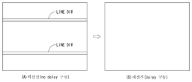
도 1 및 도 2는 본 발명의 실시예에 따른 편광 안경방식의 입체 영상 표시장치를 보여주는 도면.
도 3은 입체 영상 표시장치의 미 분할 구동 예를 보여 주는 도면.
도 4는 도 3에 도시된 픽셀의 접속 구성을 보여주는 등가 회로도.
도 5는 각 구동 모드에서 픽셀의 충전 및 방전 파형을 보여주는 도면.
도 6 및 도 7은 각각 2D 모드 및 3D 모드에서 보조 표시부의 동작을 보여주는 도면들.
도 8은 입체 영상 표시장치의 2 분할 구동 예를 보여 주는 도면.
도 9는 도 8과 같은 2 분할 구동을 위한 방전 제어전압의 파형을 보여주는 파형도.
도 10은 2 분할 구동시 도 9와 같은 방전 제어전압에 의해 초래되는 공통전압의 리플과 라인 딤을 보여주는 도면.
도 11은 도 10과 같은 라인 딤 억제를 위한 일 실시예로서, 제어전압 지연부가 추가된 방전제어전압 발생회로의 내부 구성을 보여주는 도면.
도 12는 도 11의 제어전압 지연부를 상세히 보여주는 등가 회로도.
도 13은 도 12의 제어전압 지연부를 통해 지연된 방전 제어전압의 파형과 그로 인해 공통전압의 리플이 최소화되는 것을 보여주는 도면.
도 14는 지연된 방전 제어전압이 인가되는 표시패널의 방전 제어라인들을 보여주는 도면.
도 15는 도 10과 같은 라인 딤 억제를 위한 다른 실시예로서, 방전 제어전압을 지연시키기 위해 표시패널에 구불구불하게 형성되는 방전 제어라인들을 보여주는 도면.
도 16은 방전 제어전압의 지연 여부에 따라 공통전압의 리플 크기가 달라지는 것을 보여주는 시뮬레이션 결과도면.
도 17은 방전 제어전압의 지연에 따라 라인 딤이 억제되는 것을 보여주는 도면.BRIEF DESCRIPTION OF THE DRAWINGS FIG. 1 is a perspective view of a stereoscopic image display apparatus according to an embodiment of the present invention; FIG.
3 is a diagram showing an example of non-divided driving of a stereoscopic image display apparatus.
4 is an equivalent circuit diagram showing a connection configuration of the pixel shown in Fig.
5 shows charge and discharge waveforms of pixels in each drive mode;
6 and 7 are diagrams showing the operation of the auxiliary display unit in the 2D mode and the 3D mode, respectively.
8 is a view showing an example of two-division driving of a stereoscopic image display apparatus.
Fig. 9 is a waveform diagram showing waveforms of discharge control voltages for two-division driving as shown in Fig. 8. Fig.
10 is a view showing ripples and line dimes of a common voltage caused by a discharge control voltage as shown in Fig.
FIG. 11 is a diagram showing an internal configuration of a discharge control voltage generating circuit to which a control voltage delay unit is added, as an embodiment for the line-dim suppression as shown in FIG. 10; FIG.
12 is an equivalent circuit diagram showing the control voltage delay unit of FIG. 11 in detail;
FIG. 13 is a diagram showing that the waveform of the discharge control voltage delayed through the control voltage delay unit of FIG. 12 and thereby the ripple of the common voltage is minimized; FIG.
14 is a view showing discharge control lines of a display panel to which a delayed discharge control voltage is applied;
Fig. 15 is a view showing discharge control lines formed in a wobbling shape on a display panel to delay a discharge control voltage, as another embodiment for the lint-dim suppression as shown in Fig. 10. Fig.
16 is a simulation result showing that the ripple magnitude of the common voltage is varied depending on whether or not the discharge control voltage is delayed.
17 is a view showing that the line dim is suppressed according to the delay of the discharge control voltage.
이하, 도 1 내지 도 17을 참조하여 본 발명의 바람직한 실시예에 대하여 상세히 설명하기로 한다.Hereinafter, preferred embodiments of the present invention will be described in detail with reference to FIGS. 1 to 17. FIG.
도 1 및 도 2는 본 발명의 실시예에 따른 편광 안경방식의 입체 영상 표시장치를 보여준다. 그리고, 도 3은 입체 영상 표시장치의 미 분할 구동 예를 보여준다.FIG. 1 and FIG. 2 show a polarizing glasses type stereoscopic image display apparatus according to an embodiment of the present invention. 3 shows an example of non-divided driving of the stereoscopic image display apparatus.
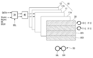
도 1 내지 도 3을 참조하면, 이 입체 영상 표시장치는 표시소자(10), 패턴드 리타더(20), 콘트롤러(30), 패널 구동회로(40) 및 편광 안경(50)을 구비한다.1 to 3, the stereoscopic image display device includes a
표시소자(10)는 액정표시소자(Liquid Crystal Display, LCD), 전계 방출 표시소자(Field Emission Display, FED), 플라즈마 디스플레이 패널(Plasma Display Panel, PDP), 및 무기 전계발광소자와 유기발광다이오드소자(Organic Light Emitting Diode, OLED)를 포함한 전계발광소자(Electroluminescence Device, EL), 전기영동 표시소자(Electrophoresis, EPD) 등의 평판 표시소자로 구현될 수 있다. 이하에서, 표시소자(10)를 액정표시소자를 중심으로 설명한다.The
표시소자(10)는 표시패널(11)과, 상부 편광필름(Polarizer)(11a)과, 하부 편광필름(11b)을 포함한다. The
표시패널(11)은 2D 모드에서 2D 영상을 표시하고, 3D 모드에서 3D 영상을 표시한다. 표시패널(11)은 두 장의 유리기판들과 이들 사이에 형성된 액정층을 포함한다. 표시패널(11)의 하부 유리기판에는 다수의 데이터라인들(DL), 이 데이터라인들(DL)과 각각 교차되는 다수의 게이트라인들(GL), 공통전압(Vcom)이 공급되는 공통라인(CL), 방전 제어전압(V3D)이 공급되는 방전 제어라인(CONL)이 형성된다. The
표시패널(11)의 상부 유리기판 상에는 블랙매트릭스, 컬러필터가 형성된다. 표시패널(11)의 상부 유리기판과 하부 유리기판 각각에는 상부 및 하부 편광필름(11a, 11b)이 부착되고 액정의 프리틸트각(pre-tilt angle)을 설정하기 위한 배향막이 형성된다. 공통전압(Vcom)이 공급되는 공통전극은 TN(Twisted Nematic) 모드와 VA(Vertical Alignment) 모드와 같은 수직전계 구동방식에서 상부 유리기판 상에 형성될 수 있으며, IPS(In Plane Switching) 모드와 FFS(Fringe Field Switching) 모드와 같은 수평전계 구동방식에서 화소전극과 함께 하부 유리기판 상에 형성될 수 있다. 유리기판들 사이에는 액정셀의 셀갭(Cell gap)을 유지하기 위한 컬럼 스페이서가 형성될 수 있다.On the upper glass substrate of the
이러한 본 발명의 표시소자(10)는 투과형 표시소자, 반투과형 표시소자, 반사형 표시소자 등 어떠한 형태로도 구현될 수 있다. 투과형 표시소자와 반투과형 표시소자에서는 백라이트 유닛(12)이 필요하다. 백라이트 유닛(12)은 직하형(direct type) 백라이트 유닛 또는, 에지형(edge type) 백라이트 유닛으로 구현될 수 있다. The
신호라인들(DL,GL)의 교차 구조에 의해 표시패널(11)에는 다수의 단위 픽셀들을 포함한 픽셀 어레이가 형성된다. 단위 픽셀은 각각 적색(R), 녹색(G) 및 청색(B) 구현을 위한 3개의 픽셀들(PIX)을 구비한다. 픽셀들(PIX) 각각은 도 4와 같이 메인 표시부(MP)와 액티브 블랙 스트라이프로 기능하는 보조 표시부(SP)를 포함한다. 보조 표시부들(SP)은 도 3과 같은 미 분할 구동에 대응하여 방전 제어라인(CONL)에 공통으로 연결될 수 있다. 방전 제어라인(CONL)은 보조 표시부들(SP)의 방전 동작을 제어하기 위한 방전 제어전압(V3D)을 보조 표시부들(SP)의 방전 제어 TFT(도 4의 DST)에 인가한다. A pixel array including a plurality of unit pixels is formed on the
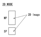
메인 픽셀부(MP)는 2D 모드에서 2D 영상의 비디오 데이터를 표시하고, 3D 모드에서 3D 영상의 비디오 데이터를 표시한다. 이에 비하여, 보조 표시부(SP)는 2D 모드에서 2D 영상의 비디오 데이터를 표시하는 역할을 하는 반면, 3D 모드에서 블랙 계조를 표시하여 블랙 스트라이프 역할을 한다. 보조 표시부(SP)는 2D 모드에서 2D 영상의 개구율과 휘도를 높이고 3D 모드에서 3D 영상의 상하 시야각을 확대한다. 1 픽셀(PIX) 내에서 메인 픽셀부(MP)와 서브 표시부(SP)의 크기와 형태는 패널 구동 특성, 표시 영상의 휘도, 3D 영상의 시야각, 응용 제품 특성 등을 고려하여 적절히 설계될 수 있다.The main pixel unit MP displays the video data of the 2D image in the 2D mode and the video data of the 3D image in the 3D mode. On the other hand, the auxiliary display unit SP serves to display video data of a 2D image in the 2D mode, while displaying black gradation in the 3D mode to serve as a black stripe. The auxiliary display unit (SP) increases the aperture ratio and brightness of the 2D image in the 2D mode and enlarges the upper and lower viewing angles of the 3D image in the 3D mode. The size and shape of the main pixel unit MP and the sub display unit SP within one pixel PIX can be appropriately designed in consideration of the panel driving characteristic, the brightness of the display image, the viewing angle of the 3D image, .
패턴드 리타더(20)는 표시패널(11)의 상부 편광필름(11a)에 부착된다. 패턴드 리타더(20)의 기수 라인들에는 제1 리타더(RT1)가 형성되고, 패턴드 리터더(20)의 우수 라인들에는 제2 리타더(RT2)가 형성된다. 제1 리타더(RT1)의 광흡수축과 제2 리타더(RT2)의 광흡수축은 서로 다르다. 패턴드 리타더(20)의 제1 리타더(RT1)는 픽셀 어레이의 기수번째 수평 픽셀라인과 대향하고, 제2 리타더(RT2)는 픽셀 어레이의 우수번째 수평 픽셀라인과 대향한다. 제1 리타더(RT1)는 상부 편광필름(11a)을 통해 입사되는 선편광의 위상을 1/4 파장 만큼 지연시켜 제1 편광(예컨대, 좌원편광)으로 통과시킨다. 제2 리타더(RT2)는 상부 편광필름(11a)을 통해 입사되는 선편광의 위상을 3/4 파장 만큼 지연시켜 제2 편광(예컨대, 우원편광)으로 통과시킨다. The patterned
콘트롤러(30)는 모드 선택신호(SEL)에 따라 2D 모드 또는 3D 모드로 패널 구동회로(40)의 동작을 제어한다. 콘트롤러(30)는 터치 스크린, 온 스크린 디스플레이(On screen display, OSD), 키보드, 마우스, 리모트 콘트롤러(Remote controller)와 같은 유저 인터페이스를 통해 모드 선택신호(SEL)를 입력받고, 그에 따라 2D 모드 동작과 3D 모드 동작을 전환할 수 있다. 한편, 콘트롤러(30)는 입력 영상의 데이터에 인코딩된 2D/3D 식별 코드 예를 들면, 디지털 방송 규격의 EPG(Electronic Program Guide) 또는 ESG(Electronic Service Guide)에 코딩될 수 있는 2D/3D 식별코드를 검출하여 2D 모드와 3D 모드를 구분할 수도 있다. The
콘트롤러(30)는 3D 모드 하에서 비디오 소스로부터 입력되는 3D 영상 데이터를 좌안 영상의 RGB 데이터와 우안 영상의 RGB 데이터로 분리한 후, 좌안 영상의 RGB 데이터와 우안 영상의 RGB 데이터를 데이터 드라이버(41)에 공급한다. 콘트롤러(30)는 2D 모드 하에서 비디오 소스로부터 입력되는 2D 영상의 RGB 데이터를 데이터 드라이버(41)에 공급한다.The
콘트롤러(30)는 수직 동기신호(Vsync), 수평 동기신호(Hsync), 데이터 인에이블 신호(Data Enable, DE), 도트 클럭(DCLK) 등의 타이밍신호들을 이용하여 패널 구동회로(40)의 동작 타이밍을 제어하기 위한 제어신호들을 발생한다. The
데이터 드라이버(41)의 동작 타이밍을 제어하기 위한 데이터 제어신호는 1 수평라인분의 데이터가 표시되는 1 수평기간 중에서 데이터의 시작점을 지시하는 소스 스타트 펄스(Source Start Pulse : SSP), 라이징(Rising) 또는 폴링(Falling) 에지에 기준하여 데이터의 래치동작을 제어하는 소스 샘플링 클럭(Source Sampling Clock : SSC), 데이터 드라이버(41)의 출력을 제어하는 소스 출력 인에이블신호(SOE), 및 표시패널(11)의 액정셀들에 공급될 데이터전압의 극성을 제어하는 극성제어신호(POL) 등을 포함한다.The data control signal for controlling the operation timing of the
게이트 드라이버(42)의 동작 타이밍을 제어하기 위한 게이트 제어신호는 한 화면이 표시되는 1 수직기간 중에서 스캔이 시작되는 시작 수평라인을 지시하는 게이트 스타트 펄스(Gate Start Pulse : GSP), 게이트 드라이버(42) 내의 쉬프트 레지스터에 입력되어 게이트 스타트 펄스(GSP)를 순차적으로 쉬프트시키기 위한 게이트 쉬프트 클럭신호(Gate Shift Clock : GSC), 및 게이트 드라이버(42)의 출력을 제어하는 게이트 출력 인에이블신호(Gate Output Enable : GOE) 등을 포함한다. The gate control signal for controlling the operation timing of the
콘트롤러(30)는 입력 프레임 주파수에 동기되는 타이밍신호들(Vsync,Hsync,DE,DCLK)을 체배하여 N×f(N은 2이상의 양의 정수, f는 입력 프레임 주파수)Hz의 프레임 주파수로 패널 구동회로(40)의 동작을 제어할 수 있다. 입력 프레임 주파수는 NTSC(National Television Standards Committee) 방식에서 60Hz이며, PAL(Phase-Alternating Line) 방식에서 50Hz이다. The
패널 구동회로(40)는 표시패널(11)의 데이터라인들(DL)을 구동시키기 위한 데이터 드라이버(41)와, 표시패널(11)의 게이트라인들(GL)을 구동시키기 위한 게이트 드라이버(42)와, 표시패널(11)의 방전 제어라인(CONL)을 구동시키기 위한 방전제어전압 발생회로(43)를 포함한다.The
데이터 드라이버(41)의 구동 IC들 각각은 쉬프트 레지스터(Shift register), 래치(Latch), 디지털-아날로그 변환기(Digital to Analog convertor, DAC), 출력 버퍼(Output buffer) 등을 포함한다. 데이터 드라이버(41)는 데이터 제어신호(SSP,SSC,SOE)에 따라 2D 또는 3D 영상의 RGB 데이터를 래치한다. 데이터 드라이버(41)는 극성제어신호(POL)에 응답하여 2D 또는 3D 영상의 RGB 데이터를 아날로그 정극성 감마보상전압과 부극성 감마보상전압으로 변환하여 데이터전압의 극성을 반전시킨다. 데이터 드라이버(41)는 게이트 드라이버(42)로부터 출력되는 스캔펄스(또는, 게이트펄스)에 동기되도록 데이터전압을 데이터라인들(DL)에 출력한다. 데이터 드라이버(41)의 구동 IC들은 TAB(Tape Automated Bonding) 공정에 의해 표시패널(11)의 하부 유리기판에 접합될 수 있다.Each of the driving ICs of the
게이트 드라이버(42)는 게이트 제어신호(GSP,GSC,GOE)에 따라 게이트 하이 전압과 게이트 로우 전압 사이에서 스윙되는 스캔펄스를 발생한다. 그리고, 게이트 제어신호(GSP,GSC,GOE)에 따라 스캔펄스를 게이트라인들(GL)에 라인 순차 방식으로 공급한다. 게이트 드라이버(42)는 게이트 쉬프트 레지스터 어레이(Gate shift register array)등을 포함한다. 게이트 드라이버(42)의 게이트 쉬프트 레지스터 어레이는 표시패널(11)에서 픽셀 어레이가 형성된 표시영역 바깥의 비 표시영역에 GIP(Gate In Panel) 방식으로 형성될 수 있다. GIP 방식에 의해, 게이트 쉬프트 레지스터들은 픽셀 어레이의 TFT(Thin Film Transistor) 공정에서 픽셀 어레이와 함께 형성될 수 있다. 게이트 드라이버(42)의 게이트 쉬프트 레지스터 어레이는 TAB 공정에 의해 표시패널(11)의 하부 유리기판에 접합되는 구동 IC들로 구현될 수도 있다.The
방전제어전압 발생회로(43)는 모드 선택신호(SEL)에 따라 방전 제어전압(V3D)을 서로 다르게 발생한다. 2D 모드에서 방전 제어전압(V3D)은 게이트 로우 전압과 실질적으로 동일한 레벨로 발생될 수 있다. 3D 모드에서 방전 제어전압(V3D)는 게이트 로우 전압보다 높고 게이트 하이 전압보다 낮은 슬라이트-온 레벨(slight on level)로 발생되되, 방전 제어 TFT(도 4의 DST)의 열화 억제를 위해 주기적으로 게이트 로우 전압으로 낮아질 수 있다.The discharge control
편광 안경(50)은 좌안 편광필터를 갖는 좌안(50L)과 우안 편광필터를 갖는 우안(50R)을 구비한다. 좌안 편광필터는 패턴드 리타더(20)의 제1 리타더(RT1)와 동일한 광흡수축을 가지며, 우안 편광필터는 패턴드 리타더(20)의 제2 리타더(RT2)와 동일한 광흡수축을 가진다. 예들 들면, 편광 안경(50)의 좌안 편광필터는 좌원편광 필터로 선택될 수 있고, 편광 안경(50)의 우안 편광필터는 우원편광 필터로 선택될 수 있다. 사용자는 편광 안경(50)을 통해 표시소자(10)에 공간분할 방식으로 표시된 3D 영상 데이터를 감상할 수 있다.The
도 4는 도 3에 도시된 픽셀의 접속 구성을 상세히 보여준다.Fig. 4 shows the connection configuration of the pixel shown in Fig. 3 in detail.
도 4를 참조하면, 메인 표시부(MP)는 제1 화소전극(Ep1), 이 제1 화소전극(Ep1)과 대향하여 제1 액정 커패시터(Clc1)를 구성하는 제1 공통전극(Ec1), 및 제1 스토리지 커패시터(Cst1)를 구비한다. 제1 화소전극(Ep1)은 제1 스위치(ST1)를 통해 데이터라인(DL)에 연결된다. 제1 스위치(ST1)는 스캔펄스(SCAN)에 응답하여 턴 온 됨으로써 데이터라인(DL) 상의 데이터전압(Vdata)을 제1 화소전극(Ep1)에 인가한다. 제1 스위치(ST1)의 게이트전극은 게이트라인(GL)에 접속되고, 소스전극은 데이터라인(DL)에 접속되며, 드레인전극은 제1 화소전극(Ep1)에 접속된다. 제1 공통전극(Ec1)은 공통전압(Vcom)으로 충전된 공통라인(CL)에 접속된다. 제1 스토리지 커패시터(Cst1)는 절연층을 사이에 두고 제1 화소전극(Ep1)과 공통라인(CL)의 중첩으로 형성된다. 4, the main display unit MP includes a first pixel electrode Ep1, a first common electrode Ec1 constituting a first liquid crystal capacitor Clc1 opposite to the first pixel electrode Ep1, And a first storage capacitor Cst1. The first pixel electrode Ep1 is connected to the data line DL through the first switch ST1. The first switch ST1 applies a data voltage Vdata on the data line DL to the first pixel electrode Ep1 by being turned on in response to the scan pulse SCAN. The gate electrode of the first switch ST1 is connected to the gate line GL, the source electrode thereof is connected to the data line DL, and the drain electrode thereof is connected to the first pixel electrode Ep1. The first common electrode Ec1 is connected to the common line CL charged with the common voltage Vcom. The first storage capacitor Cst1 is formed by overlapping the first pixel electrode Ep1 and the common line CL with an insulating layer interposed therebetween.
보조 표시부(SP)는 제2 화소전극(Ep2), 이 제2 화소전극(Ep2)과 대향하여 제2 액정 커패시터(Clc2)를 구성하는 제2 공통전극(Ec2), 및 제2 스토리지 커패시터(Cst2)를 구비한다. 제2 화소전극(Ep2)은 제2 스위치(ST2)를 통해 데이터라인(DL)에 연결된다. 제2 스위치(ST2)는 스캔펄스(SCAN)에 응답하여 턴 온 됨으로써 데이터라인(DL) 상의 데이터전압(Vdata)을 제2 화소전극(Ep2)에 인가한다. 제2 스위치(ST2)의 게이트전극은 게이트라인(GL)에 접속되고, 소스전극은 데이터라인(DL)에 접속되며, 드레인전극은 제2 화소전극(Ep2)에 접속된다. 제2 공통전극(Ec2)은 공통전압(Vcom)으로 충전된 공통라인(CL)에 접속된다. 제2 스토리지 커패시터(Cst2)는 절연층을 사이에 두고 제2 화소전극(Ep2)과 공통라인(CL)의 중첩으로 형성된다. The auxiliary display unit SP includes a second pixel electrode Ep2, a second common electrode Ec2 constituting a second liquid crystal capacitor Clc2 opposite to the second pixel electrode Ep2, and a second common electrode Ec2 constituting a second storage capacitor Cst2 . And the second pixel electrode Ep2 is connected to the data line DL through the second switch ST2. The second switch ST2 applies a data voltage Vdata on the data line DL to the second pixel electrode Ep2 by being turned on in response to the scan pulse SCAN. The gate electrode of the second switch ST2 is connected to the gate line GL, the source electrode thereof is connected to the data line DL, and the drain electrode thereof is connected to the second pixel electrode Ep2. And the second common electrode Ec2 is connected to the common line CL charged with the common voltage Vcom. The second storage capacitor Cst2 is formed by overlapping the second pixel electrode Ep2 and the common line CL with the insulating layer interposed therebetween.
제2 화소전극(Ep2)은 방전제어 스위치(DST)를 통해 공통라인(CL)에 연결된다. 방전제어 스위치(DST)는 방전 제어전압(V3D)에 응답하여 제2 화소전극(Ep2)과 공통라인(CL) 사이의 전류 패스를 스위칭한다. 방전제어 스위치(DST)의 게이트전극은 방전 제어라인(CONL)에 접속되고, 소스전극은 제2 화소전극(Ep2)에 접속되며, 드레인전극은 공통라인(CL)에 접속된다. 방전 제어전압(V3D)이 게이트 로우 전압(VGL)으로 인가될 때, 방전제어 스위치(DST)는 자신의 소스-드레인 간 채널을 완전히 폐쇄하여 제2 화소전극(Ep2)과 공통라인(CL) 사이의 전류 패스를 차단한다. 슬라이트-온 레벨(SOL)의 방전 제어전압(V3D)이 인가될 때, 방전제어 스위치(DST)는 자신의 소스-드레인 간 채널을 부분 개방하여 제2 화소전극(Ep2)과 공통라인(CL) 사이의 전류 패스를 부분적으로 허여한다. And the second pixel electrode Ep2 is connected to the common line CL through the discharge control switch DST. The discharge control switch DST switches the current path between the second pixel electrode Ep2 and the common line CL in response to the discharge control voltage V3D. The gate electrode of the discharge control switch DST is connected to the discharge control line CONL, the source electrode thereof is connected to the second pixel electrode Ep2, and the drain electrode thereof is connected to the common line CL. When the discharge control voltage V3D is applied to the gate-low voltage VGL, the discharge control switch DST completely closes the source-drain channel of the discharge control switch DST so that the second pixel electrode Ep2 and the common line CL Of the current path. When the discharge control voltage V3D of the slit-on level SOL is applied, the discharge control switch DST partially opens the source-drain channel of the discharge control switch DST to the second pixel electrode Ep2 and the common line CL Lt; RTI ID = 0.0 > partly < / RTI >
방전제어 스위치(DST)는 제1 및 제2 스위치(ST1,ST2)와 동일한 채널 용량을 갖도록 설계된다. 따라서, 방전제어 스위치(DST)는 게이트 하이 전압(VGH)에 비해 낮은 슬라이트-온 레벨(도 5의 SOL)의 방전 제어전압(V3D)이 인가됨에 따라, 풀 온 레벨(full on level) 보다 낮은 슬라이트 온 레벨(slight on level)로 도통된다. 제2 스위치(ST2)와 방전제어 스위치(DST)가 동시에 온 되더라도, 방전제어 스위치(DST)를 통해 흐르는 전류량은 제2 스위치(ST2)를 통해 흐르는 전류량에 비해 적다. 채널 저항은 게이트전극에 인가되는 전압에 반비례하기 때문에, 제2 스위치(ST2)와 방전제어 스위치(DST)가 동시에 온 되더라도, 방전제어 스위치(DST)의 채널 저항은 제2 스위치(ST2)의 채널 저항에 비해 크다.The discharge control switch DST is designed to have the same channel capacity as the first and second switches ST1 and ST2. Therefore, the discharge control switch DST is turned on at a higher level than the full on level as the discharge control voltage V3D of the lower slit-on level (SOL of FIG. 5) is applied as compared with the gate high voltage VGH. And is conducted at a low on-level. Even if the second switch ST2 and the discharge control switch DST are turned on at the same time, the amount of current flowing through the discharge control switch DST is smaller than the amount of current flowing through the second switch ST2. Since the channel resistance is inversely proportional to the voltage applied to the gate electrode, even if the second switch ST2 and the discharge control switch DST are turned on at the same time, the channel resistance of the discharge control switch DST becomes equal to the channel of the second switch ST2 It is larger than the resistance.
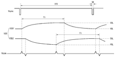
도 5는 각 구동 모드에서 픽셀(PIX)의 충전 및 방전 파형을 보여준다. 도 6은 및 도 7은 각각 2D 모드 및 3D 모드에서 보조 표시부의 동작을 보여준다. 도 5 내지 도 7을 참조하여 각 구동 모드에서 픽셀(PIX)의 동작과 함께 그의 작용 효과를 설명하면 다음과 같다.FIG. 5 shows charge and discharge waveforms of the pixel PIX in each drive mode. Fig. 6 and Fig. 7 show the operation of the auxiliary display unit in the 2D mode and the 3D mode, respectively. 5 to 7, the operation of the pixel PIX in each driving mode as well as its effect will be described below.
먼저, 2D 모드에서의 동작을 설명한다.First, the operation in the 2D mode will be described.
2D 모드에서, 방전 제어전압(V3D)은 스캔펄스(SCAN)의 게이트 로우 전압(VGL)과 동일 레벨로 발생될 수 있다. 표시패널(11)의 스위치들(도 4의 ST1,ST2)을 오프(off)시킬 수 있는 스캔펄스(SCAN)의 게이트 로우 전압(VGL)이 -5V로 선택되는 경우, 2D용 제어전압(V2D)은 -5V로 발생될 수 있다. 2D 모드에서, 방전제어 스위치(DST)는 게이트 로우 전압(VGL)의 방전 제어전압(V3D)에 응답하여 T1 및 T2 기간 동안 계속해서 턴 오프 상태를 유지한다. In the 2D mode, the discharge control voltage V3D may be generated at the same level as the gate-low voltage VGL of the scan pulse SCAN. When the gate low voltage VGL of the scan pulse SCAN capable of turning off the switches (ST1 and ST2 in Fig. 4) of the
T1 기간 동안, 게이트 하이 전압(VGH)의 스캔펄스(SCAN)에 응답하여 제1 및 제2 스위치(ST1,ST2)는 동시에 풀-온 레벨로 턴 온 된다.During the period T1, the first and second switches ST1 and ST2 are simultaneously turned on to the pull-on level in response to the scan pulse SCAN of the gate high voltage VGH.
제1 스위치(ST1)의 턴 온에 의해 메인 표시부(MP)의 제1 화소전극(Ep1)에는 2D 영상 구현을 위한 데이터전압(Vdata)이 제1 화소전압(Vp1)으로 충전되고, 제2 스위치(ST2)의 턴 온에 의해 보조 표시부(SP)의 제2 화소전극(Ep2)에도 마찬가지로 2D 영상 구현을 위한 동일한 데이터전압(Vdata)이 제2 화소전압(Vp2)으로 충전된다. 제1 및 제2 스위치(ST1,ST2)는 동일하게 설계되기 때문에, 제2 화소전압(Vp2)은 제1 화소전압(Vp1)과 실질적으로 동일하다.The data voltage Vdata for realizing the 2D image is charged to the first pixel voltage Vp1 in the first pixel electrode Ep1 of the main display unit MP by turning on the first switch ST1, The same data voltage Vdata for realizing a 2D image is similarly charged to the second pixel electrode Vp2 on the second pixel electrode Ep2 of the auxiliary display portion SP by turning on the second pixel voltage Vp2. Since the first and second switches ST1 and ST2 are designed in the same manner, the second pixel voltage Vp2 is substantially equal to the first pixel voltage Vp1.
T2 기간 동안, 게이트 로우 전압(VGL)의 스캔펄스(SCAN)에 응답하여 제1 및 제2 스위치(ST1,ST2)는 동시에 턴 오프 된다.During the period T2, the first and second switches ST1 and ST2 are simultaneously turned off in response to the scan pulse SCAN of the gate low voltage VGL.
제1 스위치(ST1)의 턴 오프에 의해, 메인 표시부(MP)의 제1 화소전극(Ep1)에 충전되어 있던 제1 화소전압(Vp1)은 킥백 전압의 영향으로 소정값만큼 쉬프트되고, 제1 스토리지 커패시터(Cst1)에 의해 이 쉬프트 된 값으로 유지된다. 제2 스위치(ST2)의 턴 오프에 의해, 보조 표시부(SP)의 제2 화소전극(Ep2)에 충전되어 있던 제2 화소전압(Vp2)은 킥백 전압의 영향으로 소정값만큼 쉬프트되고, 제2 스토리지 커패시터(Cst2)에 의해 이 쉬프트 된 값으로 유지된다. The first pixel voltage Vp1 charged in the first pixel electrode Ep1 of the main display unit MP is shifted by a predetermined value under the influence of the kickback voltage due to the turn-off of the first switch ST1, And is held at this shifted value by the storage capacitor Cst1. The second pixel voltage Vp2 charged in the second pixel electrode Ep2 of the auxiliary display unit SP is shifted by a predetermined value due to the effect of the kickback voltage due to the turn-off of the second switch ST2, And is held at this shifted value by the storage capacitor Cst2.
한편, T1 및 T2 기간에서 메인 표시부(MP)의 제1 공통전극(Ec1)과 보조 표시부(SP)의 제2 공통전극(Ec2)에는 공통라인(CL)을 통해 공통전압(Vcom)이 인가되고 있다. 제1 화소전압(Vp1)과 공통전압(Vcom) 간 전압차는 제2 화소전압(Vp2)과 공통전압(Vcom) 간 전압차와 동일하게 유지된다. 노멀리 블랙(normaly black)의 액정 모드에서 액정셀의 투과율은 화소전극과 공통전극 간 전위차에 비례한다. 그 결과, 메인 표시부(MP)와 보조 표시부(SP)는 도 6과 같이 동일 계조의 2D 영상을 구현하게 된다. 여기서, 보조 표시부(SP)에 표시되는 2D 이미지는 2D 영상의 휘도를 높이는 역할을 한다. On the other hand, in the periods T1 and T2, the common voltage Vcom is applied to the first common electrode Ec1 of the main display unit MP and the second common electrode Ec2 of the auxiliary display unit SP through the common line CL have. The voltage difference between the first pixel voltage Vp1 and the common voltage Vcom is maintained equal to the voltage difference between the second pixel voltage Vp2 and the common voltage Vcom. The transmittance of the liquid crystal cell in the liquid crystal mode of normaly black is proportional to the potential difference between the pixel electrode and the common electrode. As a result, the main display unit MP and the auxiliary display unit SP implement a 2D image of the same gradation as shown in FIG. Here, the 2D image displayed on the auxiliary display unit SP serves to increase the luminance of the 2D image.
다음으로, 3D 모드에서의 동작을 설명한다.Next, the operation in the 3D mode will be described.
3D 모드에서, 방전 제어전압(V3D)은 슬라이트-온 레벨(SOL)로 발생되되, 방전 제어 스위치(DST)의 포지티브 게이트-바이어스 스트레스(positive gate-bias stress)를 경감시키기 위해 일정 주기로 게이트 로우 전압(VGL)으로 낮아질 수 있다. 슬라이트-온 레벨(SOL)은 방전 과정에서 킥백(kick-back) 전압의 영향을 최소화하기 위해 공통전압(Vcom)보다 높고 스캔펄스(SCAN)의 게이트 하이 전압(VGH)보다 낮게 설정될 수 있다. 표시패널(11)의 스위치들(도 4의 ST1,ST2)을 풀-온(full-on) 시킬 수 있는 스캔펄스(SCAN)의 게이트 하이 전압(VGH)이 28V로 선택되고 공통전압(Vcom)이 7.5V로 선택되는 경우, 슬라이트-온 레벨(SOL)의 방전 제어전압(V3D)은 8V~12V로 발생될 수 있다. In the 3D mode, the discharge control voltage V3D is generated at the slit-on level (SOL) and is applied to the gates of the gate- Can be lowered to the voltage VGL. The slit-on level (SOL) may be set to be higher than the common voltage (Vcom) and lower than the gate high voltage (VGH) of the scan pulse (SCAN) in order to minimize the influence of the kick- . The gate high voltage VGH of the scan pulse SCAN capable of full-on switching of the switches (ST1 and ST2 in FIG. 4) of the
도 3과 같은 미 분할 구동에서, 슬라이트-온 레벨(SOL)의 방전 제어전압(V3D)이 발생되는 기간은 각 프레임에서 유효 비디오 데이터가 표시되는 표시구간에 대응될 수 있고, 게이트 로우 전압(VGL)의 방전 제어전압(V3D)이 발생되는 기간은 이웃한 표시구간들 사이의 비 표시구간 즉, 수직 블랭크 구간에 대응될 수 있다. 3, the period during which the discharge control voltage V3D of the slit-on level SOL is generated may correspond to the display period in which valid video data is displayed in each frame, and the gate-low voltage The period during which the discharge control voltage V3D of the sustain discharge control signal VGL is generated may correspond to the non-display period between the neighboring display periods, that is, the vertical blank period.
방전제어 스위치(DST)는 방전 제어전압(V3D)에 응답하여 소정 주기로 슬라이트-온 레벨의 온 상태와, 오프 상태를 반복한다. 예컨대, 방전제어 스위치(DST)는 표시기간 동안 슬라이트-온 레벨의 온 상태를 유지하고, 표시기간들 사이의 수직 블랭크기간 동안 오프 상태를 유지한다. 이하의 T1 기간 및 T2 기간은 표시기간에 속한다.The discharge control switch DST repeats the on-state and off-state of the slit-on level in a predetermined cycle in response to the discharge control voltage V3D. For example, the discharge control switch DST maintains the on-state of the slit-on level during the display period and maintains the off state during the vertical blank period between the display periods. The following T1 period and T2 period belong to the display period.
T1 기간 동안, 게이트 하이 전압(VGH)의 스캔펄스(SCAN)에 응답하여 제1 및 제2 스위치(ST1,ST2)는 동시에 풀-온 레벨로 턴 온 된다.During the period T1, the first and second switches ST1 and ST2 are simultaneously turned on to the pull-on level in response to the scan pulse SCAN of the gate high voltage VGH.
제1 스위치(ST1)의 턴 온에 의해 메인 표시부(MP)의 제1 화소전극(Ep1)에는 3D 영상 구현을 위한 데이터전압(Vdata)이 제1 화소전압(Vp1)으로 충전되고, 제2 스위치(ST2)의 턴 온에 의해 보조 표시부(SP)의 제2 화소전극(Ep2)에도 마찬가지로 3D 영상 구현을 위한 동일한 데이터전압(Vdata)이 제2 화소전압(Vp2)으로 충전된다. T1 기간에서, 풀-온 레벨의 온 상태를 갖는 제2 스위치(ST2)의 채널저항에 비해, 슬라이트-온 레벨의 온 상태를 갖는 방전제어 스위치(DST)의 채널저항은 훨씬 크다. 그 결과, 제2 화소전극(Ep2)으로부터 유출되는 방전 전류는 제2 화소전극(Ep2)으로 유입되는 충전 전류에 비해 훨씬 적게 된다. 따라서, T1 기간 동안 슬라이트-온 레벨의 온 상태를 갖는 방전제어 스위치(DST)는 제2 화소전압(Vp2)의 충전 특성에 거의 영향을 주지 않게 되고, 그 결과 제2 화소전압(Vp2)은 제1 화소전압(Vp1)에 유사한 레벨로 충전된다.The data voltage Vdata for realizing the 3D image is charged to the first pixel voltage Vp1 in the first pixel electrode Ep1 of the main display unit MP by turning on the first switch ST1, The same data voltage Vdata for realizing a 3D image is similarly charged to the second pixel electrode Vp2 on the second pixel electrode Ep2 of the auxiliary display unit SP by the turn-on of the second pixel electrode ST2. In the T1 period, the channel resistance of the discharge control switch DST having the ON state of the slit-on level is much larger than the channel resistance of the second switch ST2 having the ON state of the pull-on level. As a result, the discharge current flowing out from the second pixel electrode Ep2 becomes much smaller than the charge current flowing into the second pixel electrode Ep2. Therefore, the discharge control switch DST having the on-state of the slit-on level during the period T1 does not substantially affect the charging characteristic of the second pixel voltage Vp2, and as a result, the second pixel voltage Vp2 And is charged to a level similar to the first pixel voltage Vp1.
T2 기간 동안, 게이트 로우 전압(VGL)의 스캔펄스(SCAN)에 응답하여 제1 및 제2 스위치(ST1,ST2)는 동시에 턴 오프 된다.During the period T2, the first and second switches ST1 and ST2 are simultaneously turned off in response to the scan pulse SCAN of the gate low voltage VGL.
제1 스위치(ST1)의 턴 오프에 의해, 메인 표시부(MP)의 제1 화소전극(Ep1)에 충전되어 있던 제1 화소전압(Vp1)은 킥백 전압의 영향으로 소정값만큼 쉬프트되고, 제1 스토리지 커패시터(Cst1)에 의해 이 쉬프트 된 값으로 유지된다. 제2 스위치(ST2)의 턴 오프 되면, 보조 표시부(SP)의 제2 화소전극(Ep2)에 충전되어 있던 제2 화소전압(Vp2)은 방전제어 스위치(DST)를 경유하여 유출되는 방전 전류에 의해 소정 기간 내에 공통전압(Vcom) 레벨로 방전된다. 오프 상태를 갖는 제2 스위치(ST2)의 채널저항에 비해, 슬라이트-온 레벨의 온 상태를 갖는 방전제어 스위치(DST)의 채널저항은 훨씬 작다. 그 결과, 방전제어 스위치(DST)를 통해 제2 화소전극(Ep2)에 충전되어 있던 제2 화소전압(Vp2)은 서서히 방전되어 킥백 전압의 영향 없이 공통전압(Vcom) 레벨에 수렴된다.The first pixel voltage Vp1 charged in the first pixel electrode Ep1 of the main display unit MP is shifted by a predetermined value under the influence of the kickback voltage due to the turn-off of the first switch ST1, And is held at this shifted value by the storage capacitor Cst1. When the second switch ST2 is turned off, the second pixel voltage Vp2 charged in the second pixel electrode Ep2 of the auxiliary display unit SP is supplied to the discharging current flowing out via the discharging control switch DST To a common voltage (Vcom) level within a predetermined period. The channel resistance of the discharge control switch DST having the ON state of the slit-on level is much smaller than the channel resistance of the second switch ST2 having the OFF state. As a result, the second pixel voltage Vp2 charged in the second pixel electrode Ep2 through the discharge control switch DST is gradually discharged and converged to the common voltage Vcom level without being affected by the kickback voltage.
한편, T1 및 T2 기간에서 메인 표시부(MP)의 제1 공통전극(Ec1)과 보조 표시부(SP)의 제2 공통전극(Ec2)에는 공통전압(Vcom)이 인가되고 있다. 제2 화소전압(Vp2)의 방전이 완료된 시점에서, 제1 화소전압(Vp1)과 공통전압(Vcom) 간 전압차와 달리, 제2 화소전압(Vp2)과 공통전압(Vcom) 간 전압차는 "0"이 된다. 그 결과, 노멀리 블랙의 전위차-투과율 특성에 따라, 메인 표시부(MP)는 도 7과 같이 특정 계조의 3D 영상을 표시하게 되는 반면, 보조 표시부(SP)는 도 7과 같이 블랙 계조의 영상을 표시하여 블랙 스트라이프로 기능한다.The common voltage Vcom is applied to the first common electrode Ec1 of the main display unit MP and the second common electrode Ec2 of the auxiliary display unit SP during the periods T1 and T2. The voltage difference between the second pixel voltage Vp2 and the common voltage Vcom is different from the voltage difference between the first pixel voltage Vp1 and the common voltage Vcom when the discharge of the second pixel voltage Vp2 is completed, 0 ". As a result, according to the potential difference-transmittance characteristic of the normally black, the main display unit MP displays a 3D image of a specific grayscale as shown in Fig. 7, while the sub display unit SP displays a black grayscale image And functions as a black stripe.
보조 표시부(SP)에 표시되는 블랙 이미지는 수직으로 이웃한 3D 이미지들(즉, 좌안 이미지와 우안 이미지) 사이의 표시 간격을 넓히는 역할을 한다. 이에 따라, 별도의 블랙 스트라이프 패턴 없이도 크로스토크(Crosstalk)가 발생되지 않는 3D 상하 시야각이 상기 블랙 이미지를 통해 넓게 확보될 수 있게 된다. The black image displayed on the auxiliary display unit SP serves to widen the display interval between the vertically neighboring 3D images (i.e., the left-eye image and the right-eye image). Accordingly, a 3D vertical viewing angle in which crosstalk does not occur without a separate black stripe pattern can be ensured widely through the black image.
한편, 3D 모드에서 방전제어 스위치(DST)의 슬라이트 온 전류는 제1 및 제2 스위치(ST1,ST2)의 풀-온 전류보다 낮기 때문에 보조 표시부(SP)의 액정 커패시터(Clc2)가 블랙 계조 전압까지 방전되기까지는 소정의 시간(t0)이 필요하다. 따라서, 스캔 타이밍이 상대적으로 늦은 최하단 수평 픽셀라인의 보조 표시부들(SP)에서는 방전 기간 확보가 어려울 수 있다. 또한, 3D 모드에서 방전제어 스위치(DST)의 게이트 바이어스 스트레스를 보상하기 위하여 방전 제어전압(V3D)이 주기적으로 게이트 로우 전압(VGL)으로 떨어져야 하는 데, 방전제어 스위치(DST)의 게이트 바이어스 스트레스는 수직 블랭크 기간 정도로는 충분히 억제되기 어렵다. 방전 기간을 충분히 확보하고, 방전제어 스위치(DST)의 열화를 효과적으로 억제하기 위해 본 발명에 따른 입체 영상 표시장치는 N(N은 2이상의 양의 정수) 분할 구동될 수 있다. 이하의 설명에서는 2 분할 구동을 일 예로 설명하지만, 본 발명의 기술적 사상은 이에 한정되지 않는다.On the other hand, in the 3D mode, since the slit-on current of the discharge control switch DST is lower than the pull-on current of the first and second switches ST1 and ST2, the liquid crystal capacitor Clc2 of the sub display unit SP becomes black A predetermined time t0 is required until the voltage is discharged. Therefore, it may be difficult to secure the discharge period in the auxiliary display units SP of the lowermost horizontal pixel line in which the scan timing is relatively late. In order to compensate the gate bias stress of the discharge control switch DST in the 3D mode, the discharge control voltage V3D must periodically fall to the gate low voltage VGL, and the gate bias stress of the discharge control switch DST It is difficult to sufficiently suppress the vertical blank period. In order to sufficiently secure the discharge period and effectively suppress the deterioration of the discharge control switch DST, the stereoscopic image display apparatus according to the present invention can be driven by N (N is a positive integer of 2 or more) divided. In the following description, the two-division driving will be described as an example, but the technical idea of the present invention is not limited thereto.
도 8은 입체 영상 표시장치의 2 분할 구동 예를 보여준다. 도 9는 도 8과 같은 2 분할 구동을 위한 방전 제어전압의 파형을 보여준다. 그리고, 도 10은 2 분할 구동시 도 9와 같은 방전 제어전압에 의해 초래되는 공통전압의 리플과 라인 딤을 보여준다.FIG. 8 shows an example of two-division driving of the stereoscopic image display apparatus. FIG. 9 shows waveforms of discharge control voltages for two-division driving as shown in FIG. 10 shows ripple and line dimming of the common voltage caused by the discharge control voltage as shown in FIG. 9 in the case of two-division driving.
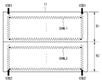
도 8 및 도 9를 참조하면, 표시패널(11)은 상하로 분할되어 제1 화면 블록(B1) 및 제2 화면 블록(B2)으로 나뉘어질 수 있다. 제1 화면 블록(B1)은 표시패널(11)에서 픽셀 어레이의 상반부에 존재하는 픽셀들을 포함하고, 제2 화면 블록(B2)은 표시패널(11)에서 픽셀 어레이의 하반부에 존재하는 픽셀들을 포함한다. 스캔펄스가 첫 번째 게이트라인으로부터 마지막 게이트라인까지 순차적으로 공급된다면, 픽셀 어레이의 하반부가 상반부보다 스캔 타이밍이 늦다. 도 8은 편의상 제1 및 제2 화면 블록들(B1, B2) 각각에 2 라인의 픽셀들을 도시하였지만, 제1 및 제2 화면 블록들(B1, B2) 각각은 2 라인 이상의 픽셀들을 포함할 수 있다는 것에 주의하여야 한다.Referring to FIGS. 8 and 9, the
방전 제어라인(CONL)은 제1 화면 블록(B1) 내의 보조 표시부들에 연결되는 제1 방전 제어라인(CONL1)과, 제2 화면 블록(B2) 내의 보조 표시부들에 연결되는 제2 방전 제어라인(CONL2)으로 분할된다. 방전 제어전압(V3D)은 제1 방전 제어전압(V3D1)과 제2 방전 제어전압(V3D2)으로 나뉘어진다.The discharge control line CONL includes a first discharge control line CONL1 connected to the sub display units in the first screen block B1 and a second discharge control line CONL1 connected to the sub display units in the second screen block B2. (CONL2). The discharge control voltage V3D is divided into a first discharge control voltage V3D1 and a second discharge control voltage V3D2.
제1 방전 제어라인(CONL1)에는 교류 형태의 제1 방전 제어전압(V3D1)이 공급된다. 제1 방전 제어전압(V3D1)은 3D 모드에서 프레임 기간의 스타트 타이밍으로부터 소정 시간(T1) 동안 슬라이트 온 레벨(SOL)로 유지된 후에 게이트 로우 전압(VGL)으로 떨어진다. 여기서, T1 시간은 1/2 프레임 기간보다 길고 1 프레임 기간(1FR)보다 짧은 시간이다. 제1 화면 블록(B1) 내에 존재하는 보조 표시부들의 방전제어 스위치들은 제1 방전 제어라인(CONL1)에 인가되는 제1 방전 제어전압(V3D1)에 의해 턴-온되어 T1 시간 동안 보조 표시부들의 전압을 충분히 블랙 계조 전압까지 방전시킨다. The first discharge control line (CONL1) is supplied with an AC first discharge control voltage (V3D1). The first discharge control voltage V3D1 falls to the gate line voltage VGL after being held at the SLLITE ON level SOL for a predetermined time T1 from the start timing of the frame period in the 3D mode. Here, T1 time is longer than 1/2 frame period and shorter than 1 frame period (1FR). The discharge control switches of the auxiliary display units existing in the first screen block B1 are turned on by the first discharge control voltage V3D1 applied to the first discharge control line CONL1 to turn on the voltages of the auxiliary display units And discharges to the black gradation voltage sufficiently.
제2 방전 제어라인(CONL2)에는 교류 형태의 제2 방전 제어전압(V3D2)이 공급된다. 제2 방전 제어전압(V3D2)은 제1 방전 제어전압(V3D1)에 비해 대략 1/2 프레임만큼 위상이 늦다. 제2 방전 제어전압(V3D2)은 3D 모드에서 대략 1/2 프레임 기간부터 슬라이트 온 레벨(SOL)로 상승하여 소정 시간(T1) 동안 이 슬라이트 온 레벨(SOL)로 유지된다. 제2 방전 제어전압(V3D2)은 스캔 타이밍이 늦은 픽셀들에 속한 보조 표시부들의 방전 시간을 충분히 확보하기 위하여 현재 프레임의 1/2 프레임 기간부터 슬라이트 온 레벨(SOL)로 상승하여 다음 프레임 기간의 스타트 타이밍으로부터 소정 시간(도 5의 t0) 이상 경과된 시점까지 이 슬라이트 온 레벨을 유지한 후에 게이트 로우 전압(VGL)으로 떨어진다. 제2 화면 블록(B2) 내에 존재하는 보조 표시부들의 방전제어 스위치들은 제2 방전 제어라인(CONL2)에 인가되는 제2 방전 제어전압(V3D2)에 의해 턴-온되어 T1 시간 동안 보조 표시부들의 전압을 충분히 블랙 계조 전압까지 방전시킨다. The second discharge control line (CONL2) is supplied with the second discharge control voltage (V3D2) in the form of an AC. The second discharge control voltage V3D2 is delayed by about 1/2 frame relative to the first discharge control voltage V3D1. The second discharge control voltage V3D2 rises from the approximately 1/2 frame period to the slit-on level SOL in the 3D mode and is maintained at the slit-on level SOL for a predetermined time T1. The second discharge control voltage V3D2 rises from the half frame period of the current frame to the slew-on level (SOL) in order to sufficiently ensure the discharge time of the auxiliary display units belonging to the pixels whose scan timing is late, And falls to the gate-low voltage (VGL) after maintaining the slit-on level from a start timing to a time point exceeding a predetermined time (t0 in Fig. 5). The discharge control switches of the auxiliary display units existing in the second screen block B2 are turned on by the second discharge control voltage V3D2 applied to the second discharge control line CONL2 so that the voltages of the auxiliary display units And discharges to the black gradation voltage sufficiently.
1 프레임 기간(1FR) 중 T1 시간을 제외한 나머지 시간 동안 제1 방전 제어전압(V3D1)이 게이트 로우 전압(VGL)으로 유지되기 때문에, 제1 화면 블록(B1) 내의 방전제어 스위치들은 게이트 바이어스 스트레스 회복에 할애되는 시간을 충분히 갖는다. 마찬가지로, 제2 방전 제어전압(V3D2)도 게이트 로우 전압(VGL)으로 유지되는 기간이 길기 때문에, 제2 화면 블록(B2) 내의 방전제어 스위치들은 게이트 바이어스 스트레스 회복에 할애되는 시간을 충분히 갖는다. Since the first discharge control voltage V3D1 is maintained at the gate low voltage VGL during the remaining time except for the T1 time in the one frame period 1FR, the discharge control switches in the first screen block B1 are subjected to gate bias stress recovery And has enough time to be devoted to. Likewise, since the period in which the second discharge control voltage V3D2 is also held at the gate low voltage VGL is long, the discharge control switches in the second screen block B2 have sufficient time to be allocated to gate bias stress recovery.
이와 같이 분할 구동의 목적은 충분한 방전 시간 확보와 함께 방전제어 스위치들의 신뢰성 제고에 있다. 그런데, 이러한 분할 구동을 위해서는 제1 방전 제어전압(V3D1)의 폴링 타이밍과 제2 방전 제어전압(V3D2)의 라이징 타이밍이 1 프레임 기간(1FR)의 시작 부분, 중간 부분 및 마지막 부분에 위치하여야 한다. 이러한 방전 제어전압들(V3D1,V3D2)의 급격한 레벨 변동은 결국 공통전압(Vcom)에 영향을 주어 공통전압(Vcom)을 순간적으로 변동시킨다. The purpose of the divided drive in this way is to increase the reliability of the discharge control switches with ensuring sufficient discharge time. However, for such divided driving, the polling timing of the first discharge control voltage V3D1 and the rising timing of the second discharge control voltage V3D2 should be located at the beginning, middle, and end of one frame period 1FR . The sudden level fluctuation of the discharge control voltages V3D1 and V3D2 eventually affects the common voltage Vcom to instantaneously vary the common voltage Vcom.
1 프레임 기간(1FR)의 시작 부분과 마지막 부분에서 발생되는 공통전압(Vcom) 리플은, 수직 블랭크 기간(VB)과 그에 근접된 기간에 대응되므로 실제로 표시 화상에 영향을 미치지 않는다. 그러나, 1 프레임 기간(1FR)의 중간 부분에서 발생되는 공통전압(Vcom) 리플은, 표시 구간에 대응되므로 표시 화상에 영향을 많이 미친다. 공통전압(Vcom)이 바뀌면 픽셀의 표시 계조는 왜곡된다. 따라서, 공통전압(Vcom)의 리플량이 커질수록 그 리플이 발생되는 영역의 표시 화상은 라인 딤 형태로 나타난다. 도 10에서, 제1 화면 블록(B1)의 라인 딤은 1 프레임 기간(1FR)의 중간 부분에서 발생되는 제1 방전 제어전압(V3D1)의 급격한 폴링에 기인하고, 제2 화면 블록(B2)의 라인 딤은 1 프레임 기간(1FR)의 중간 부분에서 발생되는 제2 방전 제어전압(V3D2)의 급격한 라이징에 기인한다.The common voltage (Vcom) ripple generated at the beginning and the end of the one frame period 1FR corresponds to the vertical blanking period VB and the period close to the vertical blanking period VB, and therefore does not actually affect the display image. However, the common voltage (Vcom) ripple generated in the middle portion of the one frame period 1FR corresponds to the display period, and therefore affects the display image much. When the common voltage Vcom is changed, the display gradation of the pixel is distorted. Therefore, as the ripple amount of the common voltage Vcom becomes larger, the display image of the region where the ripple is generated appears in a line dim shape. 10, the line dim of the first picture block B1 is caused by the abrupt polling of the first discharge control voltage V3D1 generated in the middle portion of the 1 frame period 1FR, The line dim is caused by the sudden rise of the second discharge control voltage V3D2 generated in the middle portion of the one frame period 1FR.
분할 구동시, 상기와 같은 라인 딤의 발생을 억제하기 위해서는 방전 제어전압들(V3D1,V3D2)의 레벨 변동을 완만히 해야 한다. 방전 제어전압들(V3D1,V3D2)의 레벨 변동을 완만히 하는 방법은 크게, 회로적으로 구현하는 방법과 공정적으로 구현하는 방법이 있다.In order to suppress the occurrence of the line dim during the division driving, the level of the discharge control voltages V3D1 and V3D2 must be gently varied. The method of moderating the level of the discharge control voltages V3D1 and V3D2 is largely a circuit implementation method and a process implementation method.
도 11 및 도 12는 도 10과 같은 라인 딤 억제를 위한 일 실시예로서, 제어전압 지연부가 추가된 방전제어전압 발생회로를 보여준다. 도 13은 도 12의 제어전압 지연부를 통해 지연된 방전 제어전압의 파형과 그로 인해 공통전압의 리플이 최소화되는 것을 보여준다. 그리고, 도 14는 지연된 방전 제어전압이 인가되는 표시패널의 방전 제어라인들을 보여준다.11 and 12 illustrate a discharge control voltage generating circuit to which a control voltage delay unit is added, as an embodiment for the line-dim suppression as shown in FIG. FIG. 13 shows that the waveform of the discharge control voltage delayed through the control voltage delay unit of FIG. 12 and thereby the ripple of the common voltage is minimized. 14 shows discharge control lines of a display panel to which a delayed discharge control voltage is applied.
도 11 및 도 12를 참조하면, 방전제어전압 발생회로(43)는 제어전압 발생부(431)와 제어전압 지연부(432)를 구비한다. 제어전압 발생부(431)와 제어전압 지연부(432)는 3D 보드(100)에 실장될 수 있다.11 and 12, the discharge control
제어전압 발생부(431)는 모드 선택신호(SEL)에 따라 방전 제어전압(V3D)을 서로 다르게 발생한다. 제어전압 발생부(431)는 파워 IC 및 레벨 쉬프터를 포함할 수 있다. 제어전압 발생부(431)는 2D 모드에서 파워 IC로부터 공급되는 입력 직류 전압을 레벨 쉬프팅하여 게이트 로우 전압(VGL)의 제1 및 제2 방전 제어전압(V3D1,V3D2)을 발생한다. 제어전압 발생부(431)는 3D 모드에서 콘트롤러(30)로부터 입력되는 극성제어신호(POL)와 소스 출력 인에이블신호(SOE) 등을 참조하여 하이 구간(도 9의 SOL 구간)과 로우 구간(도 9의 VGL 구간)을 포함하는 제1 및 제2 제어펄스를 발생하고, 파워 IC로부터 공급되는 입력 직류 전압을 이용하여 제1 및 제2 제어펄스를 각각 레벨 쉬프팅하여 도 9와 같이 슬라이트-온 레벨(SOL)과 게이트 로우 전압(VGL)을 교번하는 제1 및 제2 방전 제어전압(V3D1,V3D2)을 발생한다. The control
제어전압 지연부(432)는 제어전압 발생부(431)로부터 제1 및 제2 방전 제어전압(V3D1,V3D2)을 입력받고, 3D 모드에서 이 제1 및 제2 방전 제어전압(V3D1,V3D2)을 지연시켜 지연된 제1 방전 제어전압(V3D1')과 지연된 제2 방전 제어전압(V3D2')을 발생한다. 이를 위해, 제어전압 지연부(432)는 입력되는 제1 방전 제어전압(V3D1)을 지연시키기 위한 제1 지연부(432A)와 제2 방전 제어전압(V3D2)을 지연시키기 위한 제2 지연부(432B)를 포함한다.The control
제1 지연부(432A)는 제1 노드(N1)와 제2 노드(N2) 사이에 접속된 제1 저항(R1)과, 제2 노드(N2)와 그라운드 사이에 접속된 제1 커패시터(C1)를 구비한다. 제1 지연부(432A)는 제1 저항(R1)의 값과 제1 커패시터(C1)의 값의 곱으로 정의되는 시정수만큼 제1 방전 제어전압(V3D1)을 지연시킨다. 제1 지연부(432A)는 제1 노드(N1)와 제2 노드(N2) 사이에서 제1 저항(R1)과 병렬 접속되는 제1 가변저항(Rt1)을 더 구비하여 패널별 RC 편차의 조절을 용이하게 할 수 있다.The
제2 지연부(432B)는 제3 노드(N3)와 제4 노드(N4) 사이에 접속된 제2 저항(R2)과, 제4 노드(N4)와 그라운드 사이에 접속된 제2 커패시터(C2)를 구비한다. 제2 지연부(432B)는 제2 저항(R2)의 값과 제2 커패시터(C2)의 값의 곱으로 정의되는 시정수만큼 제2 방전 제어전압(V3D2)을 지연시킨다. 제2 지연부(432B)는 제3 노드(N3)와 제4 노드(N4) 사이에서 제2 저항(R2)과 병렬 접속되는 제2 가변저항(Rt2)을 더 구비하여 패널별 RC 편차의 조절을 용이하게 할 수 있다. The
제1 및 제2 저항(R1,R2)은 서로 동일한 값으로 설계되고, 제1 및 제2 커패시터(C1,C2)는 서로 동일한 값으로 설계되며, 제1 및 제2 가변저항(Rt1,Rt2)은 서로 동일한 값으로 설계된다.The first and second resistors R1 and R2 are designed to have the same value as each other. The first and second capacitors C1 and C2 are designed to have the same value. The first and second variable resistors Rt1 and Rt2, Are designed to have the same value.
제어전압 지연부(432)는 도 13과 같이, 지연된 제1 방전 제어전압(V3D1')을 제1 화면 블록(B1)의 제1 방전 제어라인(CONL1)에 공급하고, 지연된 제2 방전 제어전압(V3D2')을 제2 화면 블록(B2)의 제2 방전 제어라인(CONL2)에 공급한다. 이 경우, 제1 및 제2 방전 제어라인(CONL1,CONL2)은 직선 형태를 갖는다.The control
지연된 제1 방전 제어전압(V3D1')은 도 14와 같이 1 프레임 기간(1FR)의 T1 시간내에서 슬라이트 온 레벨(SOL)로 완만히 상승된 후, T1 시간을 제외한 1 프레임 기간(1FR)의 나머지 시간내에서 게이트 로우 전압(VGL)으로 완만히 하강한다. 지연된 제2 방전 제어전압(V3D2')은 현재 프레임의 1/2 프레임 기간부터 시작하여 다음 프레임 기간의 스타트 타이밍으로부터 소정 시간(도 5의 t0) 이상 경과된 시점까지 슬라이트 온 레벨(SOL)로 완만히 상승한 후, 상기 소정 시간(도 5의 t0) 이상 경과된 시점이후부터 게이트 로우 전압(VGL)으로 완만히 하강한다.14, the delayed first discharge control voltage V3D1 'is gradually raised to the slit-on level SOL within the T1 time of one frame period 1FR, And slowly falls to the gate low voltage (VGL) within the remaining time. The delayed second discharge control voltage V3D2 'starts from the half frame period of the current frame to the slit-on level SOL from the start timing of the next frame period to the time point exceeding the predetermined time (t0 in FIG. 5) After a gradual rise, the time point at which the predetermined time (t0 in Fig. 5) has elapsed is gradually lowered to the gate low voltage (VGL).
지연된 제1 및 제2 방전 제어전압(V3D1',V3D2')은 급격하게 폴링되거나 또는 급격하게 라이징되지 않으므로, 도 14와 같이 공통전압(Vcom)의 리플량은 크게 줄어들게 된다.Since the delayed first and second discharge control voltages V3D1 'and V3D2' are not rapidly polled or rapidly shrunk, the ripple amount of the common voltage Vcom is greatly reduced as shown in FIG.
도 15는 도 10과 같은 라인 딤 억제를 위한 다른 실시예를 보여준다.Fig. 15 shows another embodiment for the rhythm suppression as shown in Fig.
도 15를 참조하면, 도 9와 같이 급격하게 폴링되거나 라이징되는 제1 방전 제어전압(V3D1)을 지연시키기 위해, 본 발명은 제1 화면 블록(B1)에서 제1 방전 제어라인(CONL1)을 구불 구불한 곡선 형태로 형성함과 아울러 제1 방전 제어라인(CONL1)의 일측과 그라운드 사이에 제1 커패시터(C1)을 형성할 수 있다. 또한, 본 발명은 도 9와 같이 급격하게 폴링되거나 라이징되는 제2 방전 제어전압(V3D2)을 지연시키기 위해, 제2 화면 블록(B2)에서 제2 방전 제어라인(CONL2)을 구불 구불한 곡선 형태로 형성함과 아울러 제2 방전 제어라인(CONL2)의 일측과 그라운드 사이에 제2 커패시터(C2)를 형성할 수 있다. 이에 의해, 제1 방전 제어전압(V3D1)은 제1 화면 블록(B1)에서 도 14의 V3D1'과 같은 형태로 지연될 수 있으며, 제2 방전 제어전압(V3D2)은 제2 화면 블록(B2)에서 도 14의 V3D2'와 같은 형태로 지연될 수 있다. Referring to FIG. 15, in order to delay the first discharge control voltage V3D1 which is abruptly polled or grounded as shown in FIG. 9, the present invention is a method of delaying the first discharge control line CONL1 in the first screen block B1 A first capacitor C1 may be formed between one side of the first discharge control line CONL1 and the ground. In order to delay the second discharge control voltage V3D2, which is rapidly polled or grounded, as shown in FIG. 9, the second discharge control line CONL2 in the second screen block B2 may be curved And a second capacitor C2 may be formed between one side of the second discharge control line CONL2 and the ground. Thus, the first discharge control voltage V3D1 may be delayed in the first screen block B1 in the same manner as V3D1 'in FIG. 14, and the second discharge control voltage V3D2 may be delayed in the second screen block B2, In the same manner as V3D2 'in Fig.
도 16은 방전 제어전압의 지연 여부에 따라 공통전압의 리플 크기가 달라지는 것을 보여주는 시뮬레이션 결과이다. 그리고, 도 17은 방전 제어전압의 지연에 따라 라인 딤이 억제되는 것을 보여준다.16 is a simulation result showing that the ripple magnitude of the common voltage varies depending on whether the discharge control voltage is delayed or not. 17 shows that the line dim is suppressed according to the delay of the discharge control voltage.
도 16의 결과를 통해 쉽게 알 수 있듯이, 공통전압(Vcom)의 리플량은 지연된 제1 및 제2 방전 제어전압(V3D1',V3D2')에 의해 큰 폭으로 줄어들고 있다. 공통전압(Vcom)의 리플량이 줄어들면, 도 17과 같이 제1 및 제2 화면 블록(B1,B2)의 라인 딤은 억제될 수 있다.
As is clear from the results of FIG. 16, the amount of ripple of the common voltage Vcom is greatly reduced by the delayed first and second discharge control voltages V3D1 'and V3D2'. If the amount of the ripple of the common voltage Vcom is reduced, the line dim of the first and second picture blocks B1 and B2 can be suppressed as shown in Fig.
상술한 바와 같이, 본 발명에 따른 입체 영상 표시장치는 보조 표시부들(액티브 블랙 스트라이프들)의 방전 기간을 충분히 확보하고, 보조 표시부들에 구비된 방전제어 스위치들의 열화를 효과적으로 억제하기 위해 표시패널을 N(N은 2이상의 양의 정수) 분할 구동시킨다. 본 발명에 따른 입체 영상 표시장치는 분할 구동시 제어전압 지연부를 통해 방전 제어전압을 미리 지연시켜 표시패널에 인가하거나 또는, 방전 제어전압이 표시패널에 인가된 후 지연되도록 방전 제어라인을 형성함으로써, 분할 구동시 문제되는 라인 딤을 효과적으로 억제시킬 수 있다.As described above, in the stereoscopic image display apparatus according to the present invention, in order to sufficiently secure the discharge period of the auxiliary display units (active black stripes) and effectively suppress the deterioration of the discharge control switches provided in the auxiliary display units, N (N is a positive integer equal to or larger than 2). The present invention provides a three-dimensional image display apparatus comprising: a discharge control voltage generating unit for generating a discharge control voltage by applying a discharge control voltage to a display panel through a control voltage delay unit in a divided driving mode or by delaying a discharge control voltage applied to a display panel, It is possible to effectively suppress the line dim which is a problem in the divided driving.
이상 설명한 내용을 통해 당업자라면 본 발명의 기술사상을 일탈하지 아니하는 범위 내에서 다양한 변경 및 수정이 가능함을 알 수 있을 것이다. 따라서, 본 발명은 상세한 설명에 기재된 내용으로 한정되는 것이 아니라 특허 청구의 범위에 의해 정하여져야만 할 것이다. It will be apparent to those skilled in the art that various modifications and variations can be made in the present invention without departing from the spirit or scope of the invention. Therefore, the present invention should not be limited to the details described in the detailed description, but should be defined by the claims.
10 : 표시소자 11 : 표시패널
20 : 패턴드 리타더 30 : 콘트롤러
40 : 패널 구동회로 41 : 데이터 드라이버
42 : 게이트 드라이버 43 : 방전제어전압 발생회로
50 : 편광 안경 100 : 3D 보드
431 : 제어전압 발생부 432 : 제어전압 지연부10: display element 11: display panel
20: pattern-retarder 30: controller
40: panel driving circuit 41: data driver
42: Gate driver 43: Discharge control voltage generating circuit
50: polarizing glasses 100: 3D board
431: Control voltage generator 432: Control voltage delay unit
Claims (8)
광흡수축이 서로 다른 제1 리타더와 제2 리타더를 포함하되, 상기 제1 리타더는 상기 표시 패널의 기수 번째 수평 픽셀 라인 또는 우수 번째 수평 픽셀 라인 중 하나에 대향하고 상기 제2 리타더는 다른 하나에 대향하는, 패턴드 리타더;
2D 모드에서 2D 영상의 데이터전압을 상기 데이터라인들에 공급하고 3D 모드에서 3D 영상의 데이터 전압을 상기 데이터라인들에 공급하는 데이터 구동회로;
상기 2D 모드와 상기 3D 모드에서 게이트 로우 전압과 게이트 하이 전압 사이에서 스윙하는 스캔펄스를 게이트라인들에 순차적으로 공급하는 게이트 구동회로;
상기 2D 모드에서 상기 게이트 로우 전압과 동일 레벨로 제1 및 제2 방전 제어전압을 발생시키고, 상기 3D 모드에서 상기 제1 화면 블록의 보조 표시부의 방전을 제어하기 위한 제1 방전 제어전압을 제1 교류 파형으로 발생시키고 상기 제2 화면 블록의 보조 표시부의 방전을 제어하기 위한 제2 방전 제어전압을 상기 제1 교류 파형에 비해 1/2 프레임만큼 위상이 늦은 제2 교류 파형으로 발생시키는, 제어전압 발생부; 및
상기 제1 방전 제어전압을 서서히 상승시키고 서서히 하강시키는 방식으로 지연시켜 상기 제1 방전 제어라인에 인가하고, 상기 제2 방전 제어전압을 서서히 상승시키고 서서히 하강시키는 방식으로 지연시켜 상기 제2 방전 제어라인에 인가하는 제어전압 지연부를 구비하는 것을 특징으로 하는 입체 영상 표시장치.And an auxiliary display unit including a data line, gate lines intersecting with the data lines, and a main display unit and a second switch, each of which includes a first switch, through the first switch and the second switch, And a plurality of pixels connected to the lines and the scan lines and including a plurality of pixels in which the main display unit and the auxiliary display unit are vertically arranged, the display unit is divided into a first screen block and a second screen block, A display panel connected to the first discharge control line and the common line via a control switch and connected to the second discharge control line and the common line through a discharge control switch of the sub display of each pixel in the second screen block;
Wherein the first retarder is opposed to one of the odd-numbered horizontal pixel line or the odd-numbered horizontal pixel line of the display panel, and the second retarder having a light absorption axis different from the first retarder, The patterned retarder facing the other;
A data driving circuit for supplying a data voltage of a 2D image to the data lines in a 2D mode and supplying a data voltage of the 3D image to the data lines in a 3D mode;
A gate driving circuit sequentially supplying a scan pulse swinging between a gate low voltage and a gate high voltage to the gate lines in the 2D mode and the 3D mode;
The first discharge control voltage for generating the first and second discharge control voltages at the same level as the gate low voltage in the 2D mode and for controlling the discharge of the auxiliary display portion of the first screen block in the 3D mode, Generating a second discharge control voltage for generating the AC waveform and controlling the discharge of the auxiliary display portion of the second screen block to a second AC waveform that is phase-delayed by 1/2 frame as compared with the first AC waveform, Generating part; And
The first discharge control voltage is gradually increased and then gradually lowered to be applied to the first discharge control line and the second discharge control voltage is gradually increased and then gradually lowered to delay the first discharge control voltage, And a control voltage delay unit for applying a control voltage to the three-dimensional display unit.
상기 제어전압 발생부에서 발생되는 상기 제1 및 제2 방전 제어전압은 각각 상기 게이트 로우 전압보다 높고 게이트 하이 전압보다 낮은 슬라이트-온 레벨과 상기 게이트 로우 전압 레벨 사이에서 스윙되고;
상기 제1 및 제2 방전 제어전압 각각의 상기 슬라이트-온 레벨로 유지되는 기간은 상기 게이트 로우 전압 레벨로 유지되는 기간에 비해 길고;
상기 제1 방전 제어전압이 상기 슬라이트-온 레벨로 유지되는 기간은 상기 제2 방전 제어전압이 상기 슬라이트-온 레벨로 유지되는 기간과 일부분 중첩되는 것을 특징으로 하는 입체 영상 표시장치.The method according to claim 1,
The first and second discharge control voltages generated in the control voltage generator swing between a gate-low voltage level and a slit-on level that is higher than the gate-low voltage and lower than the gate-high voltage, respectively;
A period during which each of the first and second discharge control voltages is maintained at the slit-on level is longer than a period during which the voltage is maintained at the gate low voltage level;
Wherein a period during which the first discharge control voltage is maintained at the slit-on level is partially overlapped with a period during which the second discharge control voltage is maintained at the slit-on level.
상기 제어전압 지연부는,
제1 노드와 제2 노드 사이에 접속된 제1 저항과, 상기 제2 노드와 그라운드 사이에 접속된 제1 커패시터를 포함하여 상기 제1 방전 제어전압을 지연시키는 제1 지연부; 및
제3 노드와 제4 노드 사이에 접속된 제2 저항과, 상기 제4 노드와 그라운드 사이에 접속된 제2 커패시터를 포함하여 상기 제2 방전 제어전압을 지연시키는 제2 지연부를 포함하는 것을 특징으로 하는 입체 영상 표시장치.The method according to claim 1,
The control voltage delay unit includes:
A first delay unit including a first resistor connected between the first node and the second node and a first capacitor connected between the second node and the ground to delay the first discharge control voltage; And
And a second delay unit for delaying the second discharge control voltage by including a second resistor connected between the third node and the fourth node and a second capacitor connected between the fourth node and the ground, Dimensional image display device.
상기 제1 지연부는 상기 제1 노드와 상기 제2 노드 사이에서 상기 제1 저항과 병렬 접속되는 제1 가변저항을 더 포함하고;
상기 제2 지연부는 상기 제3 노드와 상기 제4 노드 사이에서 상기 제2 저항과 병렬 접속되는 제2 가변저항을 더 포함하는 것을 특징으로 하는 입체 영상 표시장치.The method of claim 3,
The first delay unit further comprises a first variable resistor connected in parallel with the first resistor between the first node and the second node;
Wherein the second delay unit further comprises a second variable resistor connected in parallel with the second resistor between the third node and the fourth node.
상기 제어전압 지연부를 통해 상기 제1 방전 제어전압은 상기 슬라이트-온 레벨로 서서히 상승한 후, 상기 게이트 로우 전압 레벨로 서서히 하강하고;
상기 제어전압 지연부를 통해 상기 제2 방전 제어전압은 상기 지연된 제1 방전 제어전압에 비해 1/2 프레임만큼의 위상차를 가지고 상기 슬라이트-온 레벨로 서서히 상승한 후, 상기 게이트 로우 전압 레벨로 서서히 하강하는 것을 특징으로 하는 입체 영상 표시장치.3. The method of claim 2,
The first discharge control voltage gradually rises to the slit-on level through the control voltage delay unit, and then gradually falls to the gate low voltage level;
The second discharge control voltage gradually increases to the slit-on level with a phase difference of 1/2 frame as compared with the delayed first discharge control voltage through the control voltage delay unit and then gradually falls to the gate low voltage level And the three-dimensional image display device.
광흡수축이 서로 다른 제1 리타더와 제2 리타더를 포함하되, 상기 제1 리타더는 상기 표시 패널의 기수 번째 수평 픽셀 라인 또는 우수 번째 수평 픽셀 라인 중 하나에 대향하고 상기 제2 리타더는 다른 하나에 대향하는, 패턴드 리타더;
2D 모드에서 2D 영상의 데이터전압을 상기 데이터라인들에 공급하고 3D 모드에서 3D 영상의 데이터 전압을 상기 데이터라인들에 공급하는 데이터 구동회로;
상기 2D 모드와 상기 3D 모드에서 게이트 로우 전압과 게이트 하이 전압 사이에서 스윙하는 스캔펄스를 게이트라인들에 순차적으로 공급하는 게이트 구동회로; 및
상기 2D 모드에서 상기 게이트 로우 전압과 동일 레벨로 제1 및 제2 방전 제어전압을 발생시켜 각각 상기 제1 및 제2 방전 제어라인에 인가하고, 상기 3D 모드에서 상기 제1 화면 블록의 보조 표시부의 방전을 제어하기 위한 제1 방전 제어전압을 제1 교류 파형으로 발생하여 상기 제1 방전 제어라인에 인가하고, 상기 제2 화면 블록의 보조 표시부의 방전을 제어하기 위한 제2 방전 제어전압을 상기 제1 교류 파형에 비해 1/2 프레임만큼 위상이 늦은 제2 교류 파형으로 발생하여 상기 제2 방전 제어라인에 인가하는, 제어전압 발생부를 구비하고;
상기 제1 방전 제어라인과 상기 제2 방전 제어라인은 구불 구불한 형태로 형성되는 것을 특징으로 하는 입체 영상 표시장치.And an auxiliary display unit including a data line, gate lines intersecting with the data lines, and a main display unit and a second switch, each of which includes a first switch, through the first switch and the second switch, And a plurality of pixels connected to the lines and the scan lines and including a plurality of pixels in which the main display unit and the auxiliary display unit are vertically arranged, the display unit is divided into a first screen block and a second screen block, A display panel connected to the first discharge control line and the common line via a control switch and connected to the second discharge control line and the common line through a discharge control switch of the sub display of each pixel in the second screen block;
Wherein the first retarder is opposed to one of the odd-numbered horizontal pixel line or the odd-numbered horizontal pixel line of the display panel, and the second retarder having a light absorption axis different from the first retarder, The patterned retarder facing the other;
A data driving circuit for supplying a data voltage of a 2D image to the data lines in a 2D mode and supplying a data voltage of the 3D image to the data lines in a 3D mode;
A gate driving circuit sequentially supplying a scan pulse swinging between a gate low voltage and a gate high voltage to the gate lines in the 2D mode and the 3D mode; And
A second discharge control voltage generating circuit for generating first and second discharge control voltages at the same level as the gate low voltage in the 2D mode and applying the first and second discharge control voltages to the first and second discharge control lines, A first discharge control voltage for controlling discharge is generated in a first AC waveform and applied to the first discharge control line and a second discharge control voltage for controlling discharge of the auxiliary display portion of the second screen block is supplied to the first discharge control line, And a control voltage generating unit for generating a second AC waveform having a phase delay of 1/2 frame with respect to one AC waveform and applying the second AC waveform to the second discharge control line;
Wherein the first discharge control line and the second discharge control line are formed in a serpentine shape.
상기 제1 화면 블록에서, 상기 제1 방전 제어라인의 일측과 그라운드 사이에 제1 커패시터가 형성되고;
상기 제2 화면 블록에서, 상기 제2 방전 제어라인의 일측과 그라운드 사이에 제2 커패시터가 형성되는 것을 특징으로 하는 입체 영상 표시장치.The method according to claim 6,
In the first screen block, a first capacitor is formed between one side of the first discharge control line and the ground;
Wherein a second capacitor is formed between one side of the second discharge control line and the ground in the second screen block.
상기 제어전압 발생부에서 발생되는 상기 제1 및 제2 방전 제어전압은 각각 상기 게이트 로우 전압보다 높고 게이트 하이 전압보다 낮은 슬라이트-온 레벨과 상기 게이트 로우 전압 레벨 사이에서 스윙되고;
상기 제1 및 제2 방전 제어전압 각각의 상기 슬라이트-온 레벨로 유지되는 기간은 상기 게이트 로우 전압 레벨로 유지되는 기간에 비해 길고;
상기 제1 방전 제어전압이 상기 슬라이트-온 레벨로 유지되는 기간은 상기 제2 방전 제어전압이 상기 슬라이트-온 레벨로 유지되는 기간과 일부분 중첩되는 것을 특징으로 하는 입체 영상 표시장치.6. The method of claim 5,
The first and second discharge control voltages generated in the control voltage generator swing between a gate-low voltage level and a slit-on level that is higher than the gate-low voltage and lower than the gate-high voltage, respectively;
A period during which each of the first and second discharge control voltages is maintained at the slit-on level is longer than a period during which the voltage is maintained at the gate low voltage level;
Wherein a period during which the first discharge control voltage is maintained at the slit-on level is partially overlapped with a period during which the second discharge control voltage is maintained at the slit-on level.
Priority Applications (5)
| Application Number | Priority Date | Filing Date | Title |
|---|---|---|---|
| KR20110090874A KR101493555B1 (en) | 2011-09-07 | 2011-09-07 | Stereoscopic image display |
| JP2012196461A JP5592920B2 (en) | 2011-09-07 | 2012-09-06 | 3D image display device |
| US13/605,730 US8866805B2 (en) | 2011-09-07 | 2012-09-06 | Stereoscopic image display |
| CN201210327848.6A CN103002301B (en) | 2011-09-07 | 2012-09-06 | Stereoscopic image display |
| EP12183357.8A EP2568710B1 (en) | 2011-09-07 | 2012-09-06 | Stereoscopic image display |
Applications Claiming Priority (1)
| Application Number | Priority Date | Filing Date | Title |
|---|---|---|---|
| KR20110090874A KR101493555B1 (en) | 2011-09-07 | 2011-09-07 | Stereoscopic image display |
Publications (2)
| Publication Number | Publication Date |
|---|---|
| KR20130027346A KR20130027346A (en) | 2013-03-15 |
| KR101493555B1 true KR101493555B1 (en) | 2015-02-16 |
Family
ID=47115260
Family Applications (1)
| Application Number | Title | Priority Date | Filing Date |
|---|---|---|---|
| KR20110090874A Expired - Fee Related KR101493555B1 (en) | 2011-09-07 | 2011-09-07 | Stereoscopic image display |
Country Status (5)
| Country | Link |
|---|---|
| US (1) | US8866805B2 (en) |
| EP (1) | EP2568710B1 (en) |
| JP (1) | JP5592920B2 (en) |
| KR (1) | KR101493555B1 (en) |
| CN (1) | CN103002301B (en) |
Families Citing this family (10)
| Publication number | Priority date | Publication date | Assignee | Title |
|---|---|---|---|---|
| US9171520B2 (en) * | 2011-11-21 | 2015-10-27 | Boe Technology Group Co., Ltd. | Array substrate, method for controlling the same and display panel including the array substrate |
| CN103472644B (en) * | 2013-09-25 | 2015-11-25 | 深圳市华星光电技术有限公司 | A kind of array base palte and display panels |
| CN103777422B (en) * | 2013-12-27 | 2018-04-10 | 深圳市华星光电技术有限公司 | Liquid crystal panel and its driving method, liquid crystal display |
| JP2017513045A (en) * | 2014-03-04 | 2017-05-25 | マスターイメージ 3ディー アジア リミテッド ライアビリティ カンパニー | Modulator for stereoscopic video apparatus and stereoscopic video apparatus using the same |
| KR102349494B1 (en) * | 2015-08-13 | 2022-01-12 | 삼성디스플레이 주식회사 | Organic light emitting display device |
| KR102338944B1 (en) * | 2017-07-31 | 2021-12-13 | 엘지디스플레이 주식회사 | Liquid crystal display device and method for driving the same |
| CN110806646B (en) * | 2018-07-20 | 2021-01-22 | 京东方科技集团股份有限公司 | Display panel, driving method thereof and display device |
| KR102687597B1 (en) * | 2018-12-28 | 2024-07-22 | 엘지디스플레이 주식회사 | Light emitting display apparatus |
| CN109559674B (en) * | 2019-01-29 | 2021-08-17 | 合肥京东方显示技术有限公司 | Shift register unit and driving method thereof, gate driving circuit and display device |
| KR102524024B1 (en) | 2021-05-18 | 2023-04-21 | 엠디티 주식회사 | Friction element welding apparatus and method thereof |
Citations (4)
| Publication number | Priority date | Publication date | Assignee | Title |
|---|---|---|---|---|
| KR20090004181A (en) * | 2007-07-06 | 2009-01-12 | 삼성전자주식회사 | Driving device of display device for 2D / 3D image compatibility and driving method thereof |
| KR20090058822A (en) * | 2007-12-05 | 2009-06-10 | 삼성전자주식회사 | Display device and display method for 3D image |
| KR20100115036A (en) * | 2009-04-17 | 2010-10-27 | 엘지디스플레이 주식회사 | Image display device |
| KR20110060272A (en) * | 2009-11-30 | 2011-06-08 | 엘지디스플레이 주식회사 | Stereoscopic Display and Driving Method |
Family Cites Families (8)
| Publication number | Priority date | Publication date | Assignee | Title |
|---|---|---|---|---|
| JP2002185983A (en) | 2000-12-13 | 2002-06-28 | Arisawa Mfg Co Ltd | Film for forming 3D image display body and 3D image display device |
| JP2005107063A (en) | 2003-09-30 | 2005-04-21 | Tohoku Pioneer Corp | Device and method for driving self-luminous display panel |
| GB0709796D0 (en) | 2007-05-22 | 2007-06-27 | Phase Focus Ltd | Three dimensional imaging |
| KR20090033534A (en) | 2007-10-01 | 2009-04-06 | 박희성 | Ventilation unit for the ventilation unit, in which the damper is formed to be adjusted wirelessly and the supply / exhaust amount is controlled |
| JP4770948B2 (en) * | 2009-03-03 | 2011-09-14 | ソニー株式会社 | Display device |
| KR101623595B1 (en) * | 2009-12-17 | 2016-05-23 | 엘지디스플레이 주식회사 | 3d image display device |
| US9013388B2 (en) * | 2010-09-22 | 2015-04-21 | Sharp Kabushiki Kaisha | Liquid crystal display device and display apparatus |
| KR101813517B1 (en) * | 2011-04-06 | 2018-01-02 | 삼성디스플레이 주식회사 | Method of driving display panel and display apparatus performing the method |
-
2011
- 2011-09-07 KR KR20110090874A patent/KR101493555B1/en not_active Expired - Fee Related
-
2012
- 2012-09-06 CN CN201210327848.6A patent/CN103002301B/en not_active Expired - Fee Related
- 2012-09-06 JP JP2012196461A patent/JP5592920B2/en not_active Expired - Fee Related
- 2012-09-06 US US13/605,730 patent/US8866805B2/en active Active
- 2012-09-06 EP EP12183357.8A patent/EP2568710B1/en not_active Not-in-force
Patent Citations (4)
| Publication number | Priority date | Publication date | Assignee | Title |
|---|---|---|---|---|
| KR20090004181A (en) * | 2007-07-06 | 2009-01-12 | 삼성전자주식회사 | Driving device of display device for 2D / 3D image compatibility and driving method thereof |
| KR20090058822A (en) * | 2007-12-05 | 2009-06-10 | 삼성전자주식회사 | Display device and display method for 3D image |
| KR20100115036A (en) * | 2009-04-17 | 2010-10-27 | 엘지디스플레이 주식회사 | Image display device |
| KR20110060272A (en) * | 2009-11-30 | 2011-06-08 | 엘지디스플레이 주식회사 | Stereoscopic Display and Driving Method |
Also Published As
| Publication number | Publication date |
|---|---|
| KR20130027346A (en) | 2013-03-15 |
| JP5592920B2 (en) | 2014-09-17 |
| US8866805B2 (en) | 2014-10-21 |
| JP2013059027A (en) | 2013-03-28 |
| CN103002301B (en) | 2015-03-11 |
| EP2568710A2 (en) | 2013-03-13 |
| EP2568710B1 (en) | 2017-05-31 |
| EP2568710A3 (en) | 2013-12-25 |
| CN103002301A (en) | 2013-03-27 |
| US20130057533A1 (en) | 2013-03-07 |
Similar Documents
| Publication | Publication Date | Title |
|---|---|---|
| KR101493555B1 (en) | Stereoscopic image display | |
| KR101446379B1 (en) | Image display device | |
| KR101446381B1 (en) | Image display device | |
| KR101868145B1 (en) | Stereoscopic image display | |
| KR101829455B1 (en) | Image display device and driving method thereof | |
| KR101885801B1 (en) | Stereoscopic image display | |
| KR101457746B1 (en) | Stereoscopic image display | |
| US9046695B2 (en) | Image display device including auxiliary display units in pixels for improving 2D/3D image display | |
| JP5583721B2 (en) | 3D image display device | |
| KR101924621B1 (en) | Image display device | |
| KR101818251B1 (en) | Stereoscopic image display | |
| KR101957971B1 (en) | Stereoscopic image display | |
| KR101780825B1 (en) | Stereoscopic image display |
Legal Events
| Date | Code | Title | Description |
|---|---|---|---|
| PA0109 | Patent application |
St.27 status event code: A-0-1-A10-A12-nap-PA0109 |
|
| R18-X000 | Changes to party contact information recorded |
St.27 status event code: A-3-3-R10-R18-oth-X000 |
|
| R18-X000 | Changes to party contact information recorded |
St.27 status event code: A-3-3-R10-R18-oth-X000 |
|
| PG1501 | Laying open of application |
St.27 status event code: A-1-1-Q10-Q12-nap-PG1501 |
|
| A201 | Request for examination | ||
| PA0201 | Request for examination |
St.27 status event code: A-1-2-D10-D11-exm-PA0201 |
|
| E902 | Notification of reason for refusal | ||
| PE0902 | Notice of grounds for rejection |
St.27 status event code: A-1-2-D10-D21-exm-PE0902 |
|
| T11-X000 | Administrative time limit extension requested |
St.27 status event code: U-3-3-T10-T11-oth-X000 |
|
| T11-X000 | Administrative time limit extension requested |
St.27 status event code: U-3-3-T10-T11-oth-X000 |
|
| P11-X000 | Amendment of application requested |
St.27 status event code: A-2-2-P10-P11-nap-X000 |
|
| P13-X000 | Application amended |
St.27 status event code: A-2-2-P10-P13-nap-X000 |
|
| E701 | Decision to grant or registration of patent right | ||
| PE0701 | Decision of registration |
St.27 status event code: A-1-2-D10-D22-exm-PE0701 |
|
| GRNT | Written decision to grant | ||
| PR0701 | Registration of establishment |
St.27 status event code: A-2-4-F10-F11-exm-PR0701 |
|
| PR1002 | Payment of registration fee |
St.27 status event code: A-2-2-U10-U11-oth-PR1002 Fee payment year number: 1 |
|
| PG1601 | Publication of registration |
St.27 status event code: A-4-4-Q10-Q13-nap-PG1601 |
|
| FPAY | Annual fee payment |
Payment date: 20180115 Year of fee payment: 4 |
|
| PR1001 | Payment of annual fee |
St.27 status event code: A-4-4-U10-U11-oth-PR1001 Fee payment year number: 4 |
|
| P22-X000 | Classification modified |
St.27 status event code: A-4-4-P10-P22-nap-X000 |
|
| FPAY | Annual fee payment |
Payment date: 20190114 Year of fee payment: 5 |
|
| PR1001 | Payment of annual fee |
St.27 status event code: A-4-4-U10-U11-oth-PR1001 Fee payment year number: 5 |
|
| P22-X000 | Classification modified |
St.27 status event code: A-4-4-P10-P22-nap-X000 |
|
| LAPS | Lapse due to unpaid annual fee | ||
| PC1903 | Unpaid annual fee |
St.27 status event code: A-4-4-U10-U13-oth-PC1903 Not in force date: 20200210 Payment event data comment text: Termination Category : DEFAULT_OF_REGISTRATION_FEE |
|
| PC1903 | Unpaid annual fee |
St.27 status event code: N-4-6-H10-H13-oth-PC1903 Ip right cessation event data comment text: Termination Category : DEFAULT_OF_REGISTRATION_FEE Not in force date: 20200210 |