KR101463936B1 - Graphene coating with excellent adhesion to the heat sink for semiconductor package and a method of manufacturing - Google Patents
Graphene coating with excellent adhesion to the heat sink for semiconductor package and a method of manufacturing Download PDFInfo
- Publication number
- KR101463936B1 KR101463936B1 KR1020130097779A KR20130097779A KR101463936B1 KR 101463936 B1 KR101463936 B1 KR 101463936B1 KR 1020130097779 A KR1020130097779 A KR 1020130097779A KR 20130097779 A KR20130097779 A KR 20130097779A KR 101463936 B1 KR101463936 B1 KR 101463936B1
- Authority
- KR
- South Korea
- Prior art keywords
- base metal
- heat sink
- chromium
- graphene
- semiconductor package
- Prior art date
- Legal status (The legal status is an assumption and is not a legal conclusion. Google has not performed a legal analysis and makes no representation as to the accuracy of the status listed.)
- Expired - Fee Related
Links
Images


Classifications
-
- H—ELECTRICITY
- H10—SEMICONDUCTOR DEVICES; ELECTRIC SOLID-STATE DEVICES NOT OTHERWISE PROVIDED FOR
- H10W—GENERIC PACKAGES, INTERCONNECTIONS, CONNECTORS OR OTHER CONSTRUCTIONAL DETAILS OF DEVICES COVERED BY CLASS H10
- H10W40/00—Arrangements for thermal protection or thermal control
-
- H—ELECTRICITY
- H10—SEMICONDUCTOR DEVICES; ELECTRIC SOLID-STATE DEVICES NOT OTHERWISE PROVIDED FOR
- H10W—GENERIC PACKAGES, INTERCONNECTIONS, CONNECTORS OR OTHER CONSTRUCTIONAL DETAILS OF DEVICES COVERED BY CLASS H10
- H10W72/00—Interconnections or connectors in packages
- H10W72/50—Bond wires
- H10W72/551—Materials of bond wires
- H10W72/552—Materials of bond wires comprising metals or metalloids, e.g. silver
- H10W72/5522—Materials of bond wires comprising metals or metalloids, e.g. silver comprising gold [Au]
-
- H—ELECTRICITY
- H10—SEMICONDUCTOR DEVICES; ELECTRIC SOLID-STATE DEVICES NOT OTHERWISE PROVIDED FOR
- H10W—GENERIC PACKAGES, INTERCONNECTIONS, CONNECTORS OR OTHER CONSTRUCTIONAL DETAILS OF DEVICES COVERED BY CLASS H10
- H10W72/00—Interconnections or connectors in packages
- H10W72/851—Dispositions of multiple connectors or interconnections
- H10W72/874—On different surfaces
- H10W72/884—Die-attach connectors and bond wires
-
- H—ELECTRICITY
- H10—SEMICONDUCTOR DEVICES; ELECTRIC SOLID-STATE DEVICES NOT OTHERWISE PROVIDED FOR
- H10W—GENERIC PACKAGES, INTERCONNECTIONS, CONNECTORS OR OTHER CONSTRUCTIONAL DETAILS OF DEVICES COVERED BY CLASS H10
- H10W74/00—Encapsulations, e.g. protective coatings
-
- H—ELECTRICITY
- H10—SEMICONDUCTOR DEVICES; ELECTRIC SOLID-STATE DEVICES NOT OTHERWISE PROVIDED FOR
- H10W—GENERIC PACKAGES, INTERCONNECTIONS, CONNECTORS OR OTHER CONSTRUCTIONAL DETAILS OF DEVICES COVERED BY CLASS H10
- H10W90/00—Package configurations
- H10W90/701—Package configurations characterised by the relative positions of pads or connectors relative to package parts
- H10W90/731—Package configurations characterised by the relative positions of pads or connectors relative to package parts of die-attach connectors
- H10W90/734—Package configurations characterised by the relative positions of pads or connectors relative to package parts of die-attach connectors between a chip and a stacked insulating package substrate, interposer or RDL
-
- H—ELECTRICITY
- H10—SEMICONDUCTOR DEVICES; ELECTRIC SOLID-STATE DEVICES NOT OTHERWISE PROVIDED FOR
- H10W—GENERIC PACKAGES, INTERCONNECTIONS, CONNECTORS OR OTHER CONSTRUCTIONAL DETAILS OF DEVICES COVERED BY CLASS H10
- H10W90/00—Package configurations
- H10W90/701—Package configurations characterised by the relative positions of pads or connectors relative to package parts
- H10W90/751—Package configurations characterised by the relative positions of pads or connectors relative to package parts of bond wires
- H10W90/754—Package configurations characterised by the relative positions of pads or connectors relative to package parts of bond wires between a chip and a stacked insulating package substrate, interposer or RDL
-
- H—ELECTRICITY
- H10—SEMICONDUCTOR DEVICES; ELECTRIC SOLID-STATE DEVICES NOT OTHERWISE PROVIDED FOR
- H10W—GENERIC PACKAGES, INTERCONNECTIONS, CONNECTORS OR OTHER CONSTRUCTIONAL DETAILS OF DEVICES COVERED BY CLASS H10
- H10W90/00—Package configurations
- H10W90/701—Package configurations characterised by the relative positions of pads or connectors relative to package parts
- H10W90/751—Package configurations characterised by the relative positions of pads or connectors relative to package parts of bond wires
- H10W90/756—Package configurations characterised by the relative positions of pads or connectors relative to package parts of bond wires between a chip and a stacked lead frame, conducting package substrate or heat sink
Landscapes
- Carbon And Carbon Compounds (AREA)
- Cooling Or The Like Of Semiconductors Or Solid State Devices (AREA)
Abstract
본 발명에 따른 그라핀코팅의 접착력이 우수한 반도체 패키지용 히트싱크 및 그 제조방법은 상기 베이스메탈(10)을 프레스금형에 안착하는 베이스준비단계(S10)와; 상기 베이스메탈(10)을 정해진 형상으로 프레스가공하는 프레스단계(S20)와; 상기 베이스메탈(10)을 1100℃이상에서 가열하여 상기 스테인레스의 내부에 구성된 탄소(C)와 크롬(Cr)을 분리하는 크롬분리가열단계(S30)와; 상기 가열된 베이스메탈(10)에 수소(H)와 질소(N)로 이루어진 분해가스(G)를 접촉시켜 상기 베이스메탈(10)의 표면으로 분리된 상기 크롬(Cr)을 산화크롬(Cr₂O₃)으로 형성시키는 크롬산화반응단계(S40)와; 상기 산화크롬(Cr₂O₃)으로 상기 베이스메탈(10)의 표면이 산화되며 석출되는 흑화처리피막단계(S50)와; 상기 흑화처리피막층(20)의 외표면에 탄소가 함유된 그라핀용액(Y)를 도포하여 상기 그라핀코팅층(30)을 형성하는 그라핀코팅단계(S60);으로 제작된 히트싱크의 표면에 흑화처리피막층을 형성한 후 그라핀코팅층을 형성하여 그라핀코팅층의 접착력을 향상시키는 효과가 있다.The heat sink for a semiconductor package and the method of manufacturing the same according to the present invention are excellent in adhesion of a graphene coating according to the present invention, comprising: a base preparation step (S10) of placing the base metal (10) on a press mold; A pressing step (S20) of pressing the base metal (10) to a predetermined shape; A chromium separation heating step (S30) of heating the base metal (10) at a temperature of 1100 DEG C or higher to separate the carbon (C) and chromium (Cr) formed in the stainless steel; And the decomposed gas G of hydrogen (H) and nitrogen (N) is brought into contact with the heated base metal 10 so that the chromium (Cr) separated on the surface of the base metal 10 is converted into chromium oxide A chromium oxidation reaction step S40; A blackening treatment step (S50) in which the surface of the base metal (10) is oxidized and precipitated with the chromium oxide (Cr2O3); A graphen coating step (S60) of applying the graphene solution (Y) containing carbon to the outer surface of the blackening treatment coat layer (20) to form the graphene coating layer (30) There is an effect that the adhesion of the graphene coating layer is improved by forming the graphene coating layer after forming the blackening treatment coat layer.
Description
본 발명은 그라핀코팅의 접착력이 우수한 반도체 패키지용 히트싱크 및 그 제조방법에 관한 것으로 보다 상세하게는 반도체 패키지에서 발생된 열을 방출하는 스테인레스재질의 히트싱크 표면에 산화크롬을 이용한 흑화처리피막층이 형성되고, 흑화처리피막층의 상부에 그라핀코팅층을 형성시키는 그라핀코팅의 접착력이 우수한 반도체 패키지용 히트싱크 및 그 제조방법에 관한 것이다.The present invention relates to a heat sink for a semiconductor package having excellent adhesion to a graphene coating and a method of manufacturing the same, and more particularly, to a heat sink for a semiconductor package which emits heat generated from a semiconductor package, And a graphene coating layer having a graphene coating layer formed on an upper part of the blackening treatment coat layer, and a method for producing the same.
근래에는 정보통신기술의 지속적인 발달과 함께 반도체 기술 또한 고도로 발달하고 있는 가운데 반도체 패키지를 소형화 및 집적화함에 있어서 반도체 패키지의 열적 문제와 전기적 그라운딩 문제가 가장 큰 해결과제로 대두되고 있었다.In recent years, along with the continuous development of information and communication technology, semiconductor technology has been highly developed. In the miniaturization and integration of the semiconductor package, the thermal problem of the semiconductor package and the electric grounding problem have been the biggest problems.
이러한 반도체 패키지의 소형화 및 집적화 경향에 따라 PBGA(Plastic Ball Grid Array) 및 FCBGA(Flip-Chip Ball Grid Array)등이 대표적으로 개발되고 있고, 상기 반도체 패키지는 칩에서 발생하는 열을 별도의 히트싱크(Heat sink)를 부착함으로써 상기한 열적 문제를 해결해 나가고 있었다.Plastic ball grid array (PBGA) and flip-chip ball grid array (FCBGA) have been typically developed in accordance with the tendency of miniaturization and integration of such a semiconductor package. The semiconductor package is a heat sink Heat sinks have been attached to solve the above-mentioned thermal problem.
또한, 종래 반도체 패키지의 고집적화를 위해서 많은 게이트(Gate)를 확보함과 동시에 전기적 안정성을 확보하기 위한 그라운딩 문제는 최근에 들어 상기한 히트싱크을 PCB기판이 그라운드영역과 전기적으로 접속시킴으로써 해결해 나가고 있는 실정이다.In addition, in order to secure a large number of gates for securing high integration of a conventional semiconductor package and to ensure electrical stability, a grounding problem has recently been solved by electrically connecting the above-described heat sink to a ground region of a PCB substrate .
여기서, 종래의 반도체 패키지에 구비되는 히트싱크의 기술문헌으로 국내등록특허공보 제10-0159985호가 개시되었다.Here, Korean Patent Registration No. 10-0159985 is disclosed as a technical document of a heat sink provided in a conventional semiconductor package.
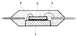
도 1은 종래의 반도체 패키지에 구비되는 히트싱크를 나타내 보인 구성도로서 도시된 바와 같이 종래의 히트싱크는 반도체 칩(C)의 회로동작시 발생하는 열을 외부로 방출하는 것을 목적으로 전기전도성과 열방출 효율이 우수한 구리(CU)재질의 일면에 니켈로 도금된 히트싱크(1)의 상부에 에폭시(4)가 도포된 후 그 상면에 반도체 칩(C)이 부착되고, 상기 반도체 칩(C)과 상기 히트싱크(1)에 연결되는 골드와이어(3)가 구비되며, 상기 반도체 칩(C)이 밀폐되도록 외부면이 몰딩되도록 구성되었다.FIG. 1 is a schematic view showing a heat sink included in a conventional semiconductor package. As shown in FIG. 1, the conventional heat sink has a structure in which a heat sink, An
그러나 종래의 반도체 패키지용 히트싱크(1)는 니켈로 도금된 히트싱크(1)의 외부면이 상기 에폭시(4)에 의하여 몰딩됨으로써, 상기 반도체 칩(C)의 하부에 부착되는 히트싱크(1)만으로 방열작용을 수행하는 것은 한계가 있었다.However, in the
또한, 종래의 반도체 패키지용 히트싱크(1)는 상기 반도체 칩(C)과 상호 견고하게 부착될 수 있도록 상기 히트싱크(1)의 표면에 다양한 재질(니켈, 팔라디움) 로 도금작업을 수행하는데 상기 히트싱크(1)의 외부에 형성된 몰딩부 또는 코팅부가 스크래치 및 절곡으로 손쉽게 박리 및 훼손되어 상품성이 떨어지는 문제점이 있었다.The conventional heat sink for
본 발명은 상기와 같은 종래 기술의 문제점을 해결하기 위해 창작된 것으로 본 발명의 목적은 반도체 패키지에서 발생된 열을 방출하는 히트싱크의 표면에 흑화처리피막층을 형성한 후 그라핀코팅층을 형성하여 히트싱크 표면의 접착력을 향상시키고, 히트싱크의 표면을 그라핀재질로 코팅하여 방열작용과 더불어 전자 및 전압의 이동성을 증가시킨 그라핀코팅의 접착력이 우수한 반도체 패키지용 히트싱크 및 그 제조방법을 제공함에 있다.SUMMARY OF THE INVENTION The present invention has been made in order to solve the above-mentioned problems of the prior art, and an object of the present invention is to provide a heat sink for heat dissipation, There is provided a heat sink for a semiconductor package having an improved adhesive force on a surface of a sink and coating the surface of the heat sink with a graphene material to provide an excellent adhesive force of a graphene coating with increased heat dissipation and increased electron and voltage mobility, have.
상기한 목적을 달성하기 위하여 본 발명에 의한 그라핀코팅의 접착력이 우수한 반도체 패키지용 히트싱크는 반도체 패키지에 실장된 칩에서 발생되는 열이 방출되도록 상기 칩의 상부를 덮어주는 히트싱크로서 상기 칩이 하측에 수용되도록 중심면이 상부로 절곡된 스테인레스재질의 베이스메탈과; 상기 베이스메탈의 외표면에 산화처리된 흑화처리피막층과; 상기 흑화처리피막층의 외표면에 상기 칩의 전자이동이 용이하도록 탄소가 함유된 그라핀코팅층;으로 이루어진 것을 특징으로 한다.According to an aspect of the present invention, there is provided a heat sink for a semiconductor package having an excellent adhesive force of a graphene coating according to the present invention, the heat sink for covering an upper portion of the chip to discharge heat generated from the chip mounted on the semiconductor package, A stainless steel base metal having a central surface bent upwardly to be received in a lower side; A blackening treatment coat layer oxidized on the outer surface of the base metal; And a carbon-containing graphene coating layer on the outer surface of the blackening treatment coat layer to facilitate electron movement of the chip.
상기 흑화처리피막층과 그라핀코팅층의 사이에는 접착력이 향상되도록 전도성을 갖는 프라이머코팅층이 포함된 것을 특징으로 한다.And a primer coating layer having conductivity so as to improve adhesion strength between the blackening treatment coat layer and the graphene coating layer.
상기한 목적을 달성하기 위한 본 발명에 의한 그라핀코팅의 접착력이 우수한 반도체 패키지용 히트싱크의 제조방법은 상기 베이스메탈을 프레스금형에 안착하는 베이스준비단계와; 상기 베이스메탈을 정해진 형상으로 프레스가공하는 프레스단계와; 상기 베이스메탈을 1100℃이상에서 가열하여 상기 스테인레스의 내부에 구성된 탄소와 크롬을 분리하는 크롬분리가열단계와; 상기 가열된 베이스메탈에 수소와 질소로 이루어진 분해가스를 접촉시켜 상기 베이스메탈의 표면으로 분리된 상기 크롬을 산화크롬으로 변화시키는 크롬산화반응단계와; 상기 산화크롬으로 상기 베이스메탈의 표면이 석출되는 흑화처리피막단계와; 상기 흑화처리피막층의 외표면에 탄소가 함유된 그라핀용액를 도포하여 상기 그라핀코팅층을 형성하는 그라핀코팅단계;으로 이루어진 것을 특징으로 한다According to another aspect of the present invention, there is provided a method of manufacturing a heat sink for a semiconductor package, the method including: a base preparing step of placing the base metal on a press mold; A pressing step of pressing the base metal to a predetermined shape; A chromium separation heating step of heating the base metal at a temperature of 1100 ° C or higher to separate carbon and chromium constituting the interior of the stainless steel; A chromium oxidation step of contacting the heated base metal with a decomposition gas of hydrogen and nitrogen to change the chromium separated into the surface of the base metal into chromium oxide; A blackening treatment step in which the surface of the base metal is precipitated with the chromium oxide; And a graphen coating step of applying the graphene solution containing carbon to the outer surface of the blackening treatment coat layer to form the graphene coating layer
상기 크롬산화반응단계의 분해가스는 상기 수소와 질소로 이루어진 암모니아가스가 사용된 것을 특징으로 한다.And the decomposition gas in the chromium oxidation reaction step is ammonia gas composed of hydrogen and nitrogen.
상기 암모니아가스는 대기중의 산소와 반응하여 75%의 수소와, 25%의 질소로 공급되는 것을 특징으로 한다.
The ammonia gas reacts with oxygen in the atmosphere and is supplied with 75% of hydrogen and 25% of nitrogen.
상기 흑화산화공정은 상기 베이스메탈의 표면을 세척하는 세척단계와; 상기 세척후 황산 또는 과산화수소가 함유된 에칭용액을 사용하여 상기 베이스메탈의 표면을 에칭하는 표면에칭단계와; 에칭된 베이스메탈을 상기 옥사이드용액에 침적하여 산화시키는 담금단계로 이루어진 것을 특징으로 한다.Wherein the blackening oxidation step includes a cleaning step of cleaning the surface of the base metal; A surface etching step of etching the surface of the base metal using an etching solution containing sulfuric acid or hydrogen peroxide after the cleaning; And immersing the etched base metal in the oxide solution to oxidize the base metal.
상기 옥사이드용액은 이산화염소로 형성된 것을 특징으로 한다.And the oxide solution is formed of chlorine dioxide.
상기 그라핀용액(Y)은 흑연분말에 에탄올이 용매로서 사용되되, 분산제로 다이페닐다이에톡시실란이 첨가되어 형성된 것을 특징으로 한다.The graphene solution (Y) is characterized in that ethanol is used as a solvent in graphite powder, and diphenyldiethoxysilane is added as a dispersant.
이와 같이 본 발명에 의한 그라핀코팅의 접착력이 우수한 반도체 패키지용 히트싱크 및 그 제조방법은 다음과 같은 효과가 있다.As described above, the heat sink for a semiconductor package and the method of manufacturing the same having the excellent adhesive force of the graphene coating according to the present invention have the following effects.
첫째, 반도체 패키지에서 발생된 열을 방출하는 히트싱크의 표면에 흑화처리피막층을 형성한 후 그라핀코팅층을 형성함으로써, 그라핀코팅층의 접착력을 향상시켜 히트싱크의 사용기간을 대폭 연장할 수 있고,First, a blackening treatment coat layer is formed on the surface of a heat sink that emits heat generated from a semiconductor package, and then a graphene coating layer is formed. Thus, the adhesive force of the graphene coating layer can be improved to greatly extend the service life of the heat sink,
둘째, 히트싱크의 표면을 그라핀코팅층을 형성함으로써, 방열작용과 더불어 전자 및 전압의 이동성을 증가시켜 반도체 패키지의 사용성을 향상시킬 수 있는 효과가 있다.Second, by forming a graphene coating layer on the surface of the heat sink, it is possible to improve the usability of the semiconductor package by increasing the electron and voltage mobility as well as the heat radiation.
도 1은 종래의 반도체 패키지용 히트싱크를 나타내 보인 구성도이고,
도 2는 본 발명에 따른 반도체 패키지용 히트싱크를 나타내 보인 구성도이며,
도 3은 도 2에 도시된 'A'를 나타내 보인 부분확대도이고,
도 4는 본 발명에 따른 반도체 패키지용 히트싱크의 제조방법을 나타내 보인 블록도이며,
도 5는 본 발명에 따른 스테인레스의 흑화처리방법을 나타내 보인 공정도이고,
도 6은 본 발명에 따른 접착강도시험의 일실시예 중 밴딩시험을 나타내 보인 시험사진표이며,
도 7은 본 발명에 따른 접착강도시험의 일실시예 중 테이핑시험을 나타내 보인 시험사진표이다.1 is a view showing a conventional heat sink for a semiconductor package,
FIG. 2 is a configuration diagram showing a heat sink for a semiconductor package according to the present invention,
3 is a partially enlarged view showing 'A' shown in FIG. 2,
4 is a block diagram showing a method of manufacturing a heat sink for a semiconductor package according to the present invention,
5 is a process diagram showing a blackening treatment method of stainless steel according to the present invention,
FIG. 6 is a photograph of a test image showing a bending test in an embodiment of the adhesive strength test according to the present invention,
Fig. 7 is a test photograph chart showing the taping test in one embodiment of the adhesive strength test according to the present invention. Fig.
이하, 첨부된 도면을 참조하여 본 발명의 일 실시예를 상세히 설명하면 다음과 같다.Hereinafter, an embodiment of the present invention will be described in detail with reference to the accompanying drawings.
본 발명에 의한 그라핀코팅의 접착력이 우수한 반도체 패키지용 히트싱크는 반도체 패키지(P)에 실장된 칩(C)에서 발생되는 열이 방출되도록 상기 칩(C)의 상부를 덮어주는 히트싱크(1)로서 도 2 내지 도 3에 도시된 바와 같이 상기 칩(C)이 하측에 수용되도록 중심면이 상부로 절곡된 스테인레스재질의 베이스메탈(10)과; 상기 베이스메탈(10)의 외표면에 산화처리된 흑화처리피막층(20)과; 상기 흑화처리피막층(20)의 외표면에 상기 칩(C)의 전자이동이 용이하도록 탄소가 함유된 그라핀코팅층(30);으로 이루어진다.The heat sink for semiconductor package having an excellent adhesive force of the graphene coating according to the present invention includes a
여기서, 상기 흑화처리피막층(20)은 스테인레스가 1100℃이상에서 가열된 후 발생된 탄소(C)와 분리된 크롬(Cr)이 물(H₂O)과 반응하여 산화크롬(Cr₂O₃)을 형성하고, 상기 산화크롬(Cr₂O₃)으로 인하여 상기 스테인레스의 표면에 다수의 요철부가 발생되는 것으로 그 화학식은 하기와 같이 확인할 수 있다.Here, the blackening
[화학식 1][Chemical Formula 1]
3H₂O + Cr = Cr₂O₃3H 2 O + Cr = Cr 2
이로 인하여 상기 산화크롬(Cr₂O₃)이 상기 스테인레스재질로 형성된 베이스메탈(10)의 표면을 석출( precipitation , 析出)함으로써 다수의 요철부가 형성된다.As a result, the surface of the
또한, 상기 그라핀코팅층(30)은 탄소원자가 2차원 평면상에서 벌집모양의 육각형으로 결합한 최초의 '2차원 결정'으로 층의 두께는 약 0.3㎚(나노미터)에 불과하며 기계적 강도가 다이아몬드의 2배에 달하고 구리보다 100배 이상 전류가 잘 흐르며 단결정 실리콘보다 100배 이상 전자를 빨리 이동시킬 수 있는 그라핀소재로 형성된다.The
여기서, 그라핀소재는 탄소원자가 5각형과 6각형으로 이루어진 축구공 모양으로 연결된 분자로 형성된 것을 말한다.Here, the graphene material is a molecule formed of a soccer ball-shaped molecule composed of a pentagon and a hexagon.
한편, 상기 흑화처리피막층(20)과 그라핀코팅층(30)의 사이에는 접착력이 향상되도록 전도성을 갖는 프라이머코팅층(40)이 포함되는 것도 바람직하다.
It is also preferable that a
상기와 같은 구성으로 이루어진 그라핀코팅의 접착력이 우수한 반도체 패키지용 히트싱크의 제조방법은 도 4 내지 도 5에 도시된 바와 같이 상기 베이스메탈(10)을 프레스금형에 안착하는 베이스준비단계(S10)와; 상기 베이스메탈(10)을 정해진 형상으로 프레스가공하는 프레스단계(S20)와; 상기 베이스메탈(10)을 1100℃이상에서 가열하여 상기 스테인레스의 내부에 구성된 탄소(C)와 크롬(Cr)을 분리하는 크롬분리가열단계(S30)와; 상기 가열된 베이스메탈(10)에 수소(H)와 질소(N)로 이루어진 분해가스(G)를 접촉시켜 상기 베이스메탈(10)의 표면으로 분리된 상기 크롬(Cr)을 산화크롬(Cr₂O₃)으로 형성시키는 크롬산화반응단계(S40)와; 상기 산화크롬(Cr₂O₃)으로 상기 베이스메탈(10)의 표면이 산화되며 석출되는 흑화처리피막단계(S50)와; 상기 흑화처리피막층(20)의 외표면에 탄소가 함유된 그라핀용액(Y)를 도포하여 상기 그라핀코팅층(30)을 형성하는 그라핀코팅단계(S60);으로 이루어진다.As shown in FIGS. 4 and 5, a method of manufacturing a heat sink for a semiconductor package having excellent adhesion to a graphene coating having the above-described structure includes a base preparation step S10 of placing the
여기서, 상기 크롬산화반응단계(S40)의 분해가스(G)는 상기 수소(H)와 질소(N)로 이루어진 암모니아가스(NH₃)가 사용된다.Here, as the decomposition gas G in the chromium oxidation reaction step S40, ammonia gas (NH3) comprising hydrogen (H) and nitrogen (N) is used.
이때, 상기 암모니아가스(NH₃)는 대기중의 산소(O₂)와 반응하여 75%의 수소(H)와, 25%의 질소(N)로 상기 베이스메탈(10)에 공급되며 이는 하기 [화학식2]와 같다. At this time, the ammonia gas (NH 3) reacts with oxygen (O 2) in the atmosphere and is supplied to the
[화학식 2](2)
2NH₃= 3H₂+ 1N₂2NH3 = 3H2 + 1N2
한편, 도 5에 도시된 바와 같이 상기 암모니아가스(NH₃)와 함께 질소가스(N₂)를 개별적으로 공급해주는 것도 바람직하다.Meanwhile, as shown in FIG. 5, it is also preferable to separately supply nitrogen gas (N.sub.2) together with the ammonia gas (NH.sub.3).
그리고, 상기 그라핀용액(Y)은 흑연분말(GP)에 에탄올이 용매로서 사용되되, 분산제로 다이페닐다이에톡시실란(diphenyldiethoxysilane)이 첨가되어 형성된다. The graphene solution (Y) is formed by adding ethanol as a solvent to graphite powder (GP), and diphenyldiethoxysilane as a dispersant.
한편, 상기 흑화산화공정(S30)이 수행된 베이스메탈(10)의 표면에 상기 그라핀용액(Y)을 코팅하는 방법으로 전기분무(electro spray coating)법이 사용되는 것이 바람직하다.The electrophoresis coating method is preferably used for coating the surface of the
여기서, 전기분무법이란 피코팅물에 전압을 인가한 후 정해진 시간동안 상기 그라핀용액(Y)을 상기 피코팅물에 분무하는 방법을 말한다.
Here, the electrospray method refers to a method of spraying the graphen solution (Y) onto the coating material for a predetermined time after applying voltage to the coating material.
상기와 같은 구성 및 방법으로 형성된 본 발명의 히트싱크에 대한 접착력시험을 통하여 본 발명의 작용효과를 설명하면 다음과 같다.Hereinafter, the operation and effect of the present invention will be described with reference to the adhesive force test for the heat sink of the present invention formed by the above-described structure and method.
1. 밴딩시험1. Bending test
가. 아래 [표 1]와 같이 비교예로서 스테인레스로 형성된 베이스메탈(1)의 표면에 그라핀코팅층(30)이 형성된 제1시험체와, 본 발명의 실시예로서 스테인레스로 형성된 베이스메탈(1)의 표면에 흑화처리피막층(20)과 그라핀코팅층(30)이 형성된 제2시험체를 각각 밴딩하여 상기 그라핀코팅층(30)의 박리여부를 평가하는 방법으로 자세한 시험방법으로 그라핀코팅된 히트싱크(1)를 가로(A), 세로(B), 대각선(C)으로 밴딩하여 상기 그라핀코팅층(30)이 베이스메탈(10)에서 박리여부를 육안으로 확인하는 방법으로 진행되었으며, 그 결과는 아래 [표 1]의 내용 및 도 6에 도시된 바와 같다. end. As a comparative example, as shown in Table 1 below, a first specimen having a
밴딩시험
Bending test
스테인레스 + 그라핀
(비교예)
Stainless + Graphene
(Comparative Example)
박리됨
Peeled
박리됨
Peeled
박리됨
Peeled
스테인레스 + 흑화산화 + 그라핀
(실시예)
Stainless steel + blackening oxidation + graphene
(Example)
박리되지않음
Not peeled
박리되지않음
Not peeled
박리되지않음
Not peeled
2. 테이핑시험2. Taping test
가. 아래 [표 2]와 같이 비교예로서 스테인레스로 형성된 베이스메탈(1)의 표면에 그라핀코팅층(30)이 형성된 제1시험체와, 본 발명의 실시예로서 스테인레스로 형성된 베이스메탈(1)의 표면에 흑화처리피막층(20)과 그라핀코팅층(30)이 형성된 제2시험체 각각의 표면에 다수의 칼집을 형성한 후 테이프를 부착하여 정해진 힘으로 뜯어내면서 상기 그라핀코팅층(30)이 테이프와 함께 박리되는 여부를 평가하는 방법으로 진행되었으며, 그 결과는 아래 [표 2]의 내용 및 도 7에 도시된 바와 같다. end. As a comparative example, as shown in the following Table 2, a first specimen in which a
테이핑
시험
Taping
exam
스테인레스 + 그라핀
(비교예)
Stainless + Graphene
(Comparative Example)
박리됨
Peeled
박리됨
Peeled
박리됨
Peeled
스테인레스 + 흑화산화 + 그라핀
(실시예)
Stainless steel + blackening oxidation + graphene
(Example)
박리되지않음
Not peeled
박리되지않음
Not peeled
박리되지않음
Not peeled
따라서, 본 발명으로 형성된 실시예는 종래에 형성되는 비교예와 비교하여 그라핀코팅층(30)의 접착력을 대폭 향상시키는 것과 더불어 기계적 강도가 탁월하고 전류와 전자의 흐름이 용이한 그라핀소재로 히트싱크를 코팅함으로써, 제품성을 향상시킬 수 있게 된다.Therefore, the embodiment formed by the present invention significantly improves the adhesive force of the
본 발명은 상술한 특정의 바람직한 실시예에 한정되지 아니하며, 청구범위에서 청구하는 본 발명의 요지를 벗어남이 없이 당해 고안이 속하는 기술분야에서 통상의 지식을 가진 자라면 누구든지 다양한 변형실시가 가능한 것은 물론이고, 그와 같은 변경은 청구범위 기재의 범위 내에 있게 된다.It will be understood by those skilled in the art that various changes in form and details may be made therein without departing from the spirit and scope of the present invention as defined by the appended claims and their equivalents. Of course, such modifications are within the scope of the claims.
<도면의 주요부분에 대한 부호의 설명>
1 : 히트싱크 10 : 베이스메탈
20 : 흑화처리피막층 30 : 그라핀코팅층
40 : 프라이머코팅층 C : 칩
P : 반도체 패키지 S10 : 베이스준비단계
S20 : 프레스단계 S30 : 크롬분리가열단계
S40 : 크롬산화반응단계 S50 : 흑화처리피막단계
S60 : 그라핀코팅단계 G : 분해가스
Y : 그라핀용액Description of the Related Art
1: Heatsink 10: Base metal
20: blackened coat layer 30: graphene coated layer
40: primer coating layer C: chip
P: semiconductor package S10: base preparation step
S20: Press step S30: Chromium separation heating step
S40: chromium oxidation reaction step S50: blackening treatment step
S60: graphene coating step G: decomposition gas
Y: Graphene solution
Claims (6)
상기 칩(C)이 하측에 수용되도록 중심면이 상부로 절곡된 스테인레스재질의 베이스메탈(10)과;
상기 베이스메탈(10)의 외표면에 흑화처리된 흑화처리피막층(20)과;
상기 흑화처리피막층(20)의 외표면에 상기 칩(C)의 전자이동이 용이하도록 탄소가 함유된 그라핀코팅층(30);으로 이루어진 것을 특징으로 하는 그라핀코팅의 접착력이 우수한 반도체 패키지용 히트싱크.A heat sink (1) for covering an upper portion of a chip (C) so that heat generated from a chip (C) mounted on a semiconductor package (P)
A stainless steel base metal 10 whose central surface is bent upward so that the chip C is received at a lower side;
A blackening treatment coat layer (20) blackened on the outer surface of the base metal (10);
And a graphene coating layer (30) containing carbon so that electrons of the chip (C) are easily transferred to the outer surface of the blackening treatment coat layer (20). Sink.
상기 흑화처리피막층(20)과 그라핀코팅층(30)의 사이에는 접착력이 향상되도록 전도성을 갖는 프라이머코팅층(40)이 포함된 것을 특징으로 하는 그라핀코팅의 접착력이 우수한 반도체 패키지용 히트싱크.The method according to claim 1,
Wherein a primer coating layer (40) having conductivity is provided between the blackening treatment coat layer (20) and the graphene coating layer (30) so as to improve the adhesive strength.
상기 베이스메탈(10)을 프레스금형에 안착하는 베이스준비단계(S10)와;
상기 베이스메탈(10)을 정해진 형상으로 프레스가공하는 프레스단계(S20)와;
상기 베이스메탈(10)을 1100℃이상에서 가열하여 상기 스테인레스의 내부에 구성된 탄소(C)와 크롬(Cr)을 분리하는 크롬분리가열단계(S30)와;
상기 가열된 베이스메탈(10)에 수소(H)와 질소(N)로 이루어진 분해가스(G)를 접촉시켜 상기 베이스메탈(10)의 표면으로 분리된 상기 크롬(Cr)을 산화크롬(Cr₂O₃)으로 변화시키는 크롬산화반응단계(S40)와;
상기 산화크롬(Cr₂O₃)으로 상기 베이스메탈(10)의 표면이 산화되며 석출되는 흑화처리피막단계(S50)와;
상기 흑화처리피막층(20)의 외표면에 탄소가 함유된 그라핀용액(Y)를 도포하여 상기 그라핀코팅층(30)을 형성하는 그라핀코팅단계(S60);으로 이루어진 것을 특징으로 하는 그라핀코팅의 접착력이 우수한 반도체 패키지용 히트싱크의 제조방법.A method of manufacturing a heat sink for a semiconductor package formed by any one of claims 1 to 2,
A base preparation step (S10) of placing the base metal (10) on a press mold;
A pressing step (S20) of pressing the base metal (10) to a predetermined shape;
A chromium separation heating step (S30) of heating the base metal (10) at a temperature of 1100 ° C or higher to separate carbon (C) and chromium (Cr) constituting the interior of the stainless steel;
And the decomposed gas G of hydrogen (H) and nitrogen (N) is brought into contact with the heated base metal 10 so that the chromium (Cr) separated on the surface of the base metal 10 is converted into chromium oxide (Step S40);
A blackening treatment step (S50) in which the surface of the base metal (10) is oxidized and precipitated with the chromium oxide (Cr2O3);
And a graphen coating step (S60) of coating the graphene solution (Y) containing carbon on the outer surface of the blackening treatment coat layer (20) to form the graphene coating layer (30). A method for manufacturing a heat sink for a semiconductor package having excellent adhesion to a coating.
상기 크롬산화반응단계(S40)의 분해가스(G)는 상기 수소(H)와 질소(N)로 이루어진 암모니아가스(NH₃)가 사용된 것을 특징으로 하는 그라핀코팅의 접착력이 우수한 반도체 패키지용 히트싱크의 제조방법.The method of claim 3,
Wherein ammonia gas (NH3) comprising hydrogen (H) and nitrogen (N) is used as the decomposition gas (G) in the chromium oxidation reaction step (S40) A method of manufacturing a sink.
상기 암모니아가스(NH₃)는 대기중의 산소(O₂)와 반응하여 75%의 수소(H)와, 25%의 질소(N)로 상기 베이스메탈(10)에 공급되는 것을 특징으로 하는 그라핀코팅의 접착력이 우수한 반도체 패키지용 히트싱크의 제조방법.5. The method of claim 4,
Wherein the ammonia gas (NH3) is supplied to the base metal (10) with 75% of hydrogen (H) and 25% of nitrogen (N) Wherein the adhesive layer is formed on the surface of the heat sink.
상기 그라핀용액(Y)은 흑연분말(GP)에 에탄올이 용매로서 사용되되, 분산제로 다이페닐다이에톡시실란(diphenyldiethoxysilane)이 첨가되어 형성된 것을 특징으로 하는 그라핀코팅의 접착력이 우수한 반도체 패키지용 히트싱크의 제조방법.The method of claim 3,
Wherein the graphene solution (Y) is formed by using graphite powder (GP) with ethanol as a solvent and diphenyldiethoxysilane as a dispersant. A method of manufacturing a heat sink.
Priority Applications (1)
| Application Number | Priority Date | Filing Date | Title |
|---|---|---|---|
| KR1020130097779A KR101463936B1 (en) | 2013-08-19 | 2013-08-19 | Graphene coating with excellent adhesion to the heat sink for semiconductor package and a method of manufacturing |
Applications Claiming Priority (1)
| Application Number | Priority Date | Filing Date | Title |
|---|---|---|---|
| KR1020130097779A KR101463936B1 (en) | 2013-08-19 | 2013-08-19 | Graphene coating with excellent adhesion to the heat sink for semiconductor package and a method of manufacturing |
Publications (1)
| Publication Number | Publication Date |
|---|---|
| KR101463936B1 true KR101463936B1 (en) | 2014-11-26 |
Family
ID=52291272
Family Applications (1)
| Application Number | Title | Priority Date | Filing Date |
|---|---|---|---|
| KR1020130097779A Expired - Fee Related KR101463936B1 (en) | 2013-08-19 | 2013-08-19 | Graphene coating with excellent adhesion to the heat sink for semiconductor package and a method of manufacturing |
Country Status (1)
| Country | Link |
|---|---|
| KR (1) | KR101463936B1 (en) |
Cited By (4)
| Publication number | Priority date | Publication date | Assignee | Title |
|---|---|---|---|---|
| CN105957978A (en) * | 2016-05-30 | 2016-09-21 | 京东方科技集团股份有限公司 | Packaging structure and manufacturing method therefor |
| WO2017111452A1 (en) * | 2015-12-21 | 2017-06-29 | 성균관대학교산학협력단 | Multilayer thin film of polymer-inorganic nanoparticle complex, and method for preparing same |
| CN114423541A (en) * | 2019-09-17 | 2022-04-29 | 石墨烯材料科技公司 | Composite powder having iron-based particles coated with graphene material |
| CN114801357A (en) * | 2022-04-28 | 2022-07-29 | 安徽碳华新材料科技有限公司 | Heat radiation structure for integrated chip based on film-like artificial graphite sheet |
Citations (1)
| Publication number | Priority date | Publication date | Assignee | Title |
|---|---|---|---|---|
| KR20050077866A (en) * | 2004-01-28 | 2005-08-04 | 삼성전자주식회사 | Semiconductor package with heat-dissipating structure and method for fabricating the same |
-
2013
- 2013-08-19 KR KR1020130097779A patent/KR101463936B1/en not_active Expired - Fee Related
Patent Citations (1)
| Publication number | Priority date | Publication date | Assignee | Title |
|---|---|---|---|---|
| KR20050077866A (en) * | 2004-01-28 | 2005-08-04 | 삼성전자주식회사 | Semiconductor package with heat-dissipating structure and method for fabricating the same |
Cited By (6)
| Publication number | Priority date | Publication date | Assignee | Title |
|---|---|---|---|---|
| WO2017111452A1 (en) * | 2015-12-21 | 2017-06-29 | 성균관대학교산학협력단 | Multilayer thin film of polymer-inorganic nanoparticle complex, and method for preparing same |
| CN105957978A (en) * | 2016-05-30 | 2016-09-21 | 京东方科技集团股份有限公司 | Packaging structure and manufacturing method therefor |
| US10439162B2 (en) | 2016-05-30 | 2019-10-08 | Boe Technology Group Co., Ltd. | Display panel, display apparatus having the same, and fabricating method thereof |
| CN114423541A (en) * | 2019-09-17 | 2022-04-29 | 石墨烯材料科技公司 | Composite powder having iron-based particles coated with graphene material |
| CN114801357A (en) * | 2022-04-28 | 2022-07-29 | 安徽碳华新材料科技有限公司 | Heat radiation structure for integrated chip based on film-like artificial graphite sheet |
| CN114801357B (en) * | 2022-04-28 | 2024-02-09 | 安徽碳华新材料科技有限公司 | Heat radiation structure for integrated chip based on film-shaped artificial graphite sheet |
Similar Documents
| Publication | Publication Date | Title |
|---|---|---|
| KR101463936B1 (en) | Graphene coating with excellent adhesion to the heat sink for semiconductor package and a method of manufacturing | |
| CN112435844A (en) | Integrated co-fired inductor and preparation method thereof | |
| US7504733B2 (en) | Semiconductor die package | |
| US20180190893A1 (en) | Thermoelectric Module | |
| CN1197292A (en) | Semiconductor device, lead frame, and lead bonding | |
| US20060032622A1 (en) | Thermal assembly and method for fabricating the same | |
| US20110284382A1 (en) | Printed circuit board and method of manufacturing the same | |
| CN109075245A (en) | Thermo-electric conversion module encapsulation | |
| TWI642160B (en) | Leadframe structure for quad flat no-lead package, quad flat no-lead package, and method of forming leadframe structure | |
| CN106847781A (en) | Power module package and its manufacture method | |
| CN108574036A (en) | Thermoelectric device and manufacturing method thereof | |
| CN116134563A (en) | Integrated Magnetics | |
| KR101482679B1 (en) | Graphene coating with excellent adhesion to the heat sink for semiconductor package and a method of manufacturing | |
| US20140191378A1 (en) | Integrated circuit package | |
| CN111312681A (en) | Semiconductor package having semiconductor die on plated conductive layer | |
| CN111540683A (en) | Manufacturing method of power device | |
| CN105612614B (en) | The manufacturing method of semiconductor device and semiconductor device | |
| CN1392602A (en) | Method for producing circuit device | |
| US20180090331A1 (en) | Method of manufacturing wafer level chip scale package | |
| CN205900519U (en) | Quiet electrical card of pottery dish device | |
| US7691679B2 (en) | Pre-plated leadframe having enhanced encapsulation adhesion | |
| JP7471374B2 (en) | Lead frames and lead frame packages | |
| US20070218284A1 (en) | Graphite product and its fabrication method | |
| Yang et al. | The study of Cu-Cu low temperature bonding using formic acid treatment with/without Pt catalyst | |
| US20150262925A1 (en) | Semiconductor device employing aluminum alloy lead-frame with anodized aluminum |
Legal Events
| Date | Code | Title | Description |
|---|---|---|---|
| PA0109 | Patent application |
St.27 status event code: A-0-1-A10-A12-nap-PA0109 |
|
| PA0201 | Request for examination |
St.27 status event code: A-1-2-D10-D11-exm-PA0201 |
|
| D13-X000 | Search requested |
St.27 status event code: A-1-2-D10-D13-srh-X000 |
|
| D14-X000 | Search report completed |
St.27 status event code: A-1-2-D10-D14-srh-X000 |
|
| E701 | Decision to grant or registration of patent right | ||
| PE0701 | Decision of registration |
St.27 status event code: A-1-2-D10-D22-exm-PE0701 |
|
| GRNT | Written decision to grant | ||
| PR0701 | Registration of establishment |
St.27 status event code: A-2-4-F10-F11-exm-PR0701 |
|
| PR1002 | Payment of registration fee |
St.27 status event code: A-2-2-U10-U11-oth-PR1002 Fee payment year number: 1 |
|
| PG1601 | Publication of registration |
St.27 status event code: A-4-4-Q10-Q13-nap-PG1601 |
|
| R18-X000 | Changes to party contact information recorded |
St.27 status event code: A-5-5-R10-R18-oth-X000 |
|
| PN2301 | Change of applicant |
St.27 status event code: A-5-5-R10-R11-asn-PN2301 |
|
| PN2301 | Change of applicant |
St.27 status event code: A-5-5-R10-R14-asn-PN2301 |
|
| FPAY | Annual fee payment |
Payment date: 20171110 Year of fee payment: 4 |
|
| PR1001 | Payment of annual fee |
St.27 status event code: A-4-4-U10-U11-oth-PR1001 Fee payment year number: 4 |
|
| FPAY | Annual fee payment |
Payment date: 20181114 Year of fee payment: 5 |
|
| PR1001 | Payment of annual fee |
St.27 status event code: A-4-4-U10-U11-oth-PR1001 Fee payment year number: 5 |
|
| PC1903 | Unpaid annual fee |
St.27 status event code: A-4-4-U10-U13-oth-PC1903 Not in force date: 20191115 Payment event data comment text: Termination Category : DEFAULT_OF_REGISTRATION_FEE |
|
| PC1903 | Unpaid annual fee |
St.27 status event code: N-4-6-H10-H13-oth-PC1903 Ip right cessation event data comment text: Termination Category : DEFAULT_OF_REGISTRATION_FEE Not in force date: 20191115 |
|
| PN2301 | Change of applicant |
St.27 status event code: A-5-5-R10-R13-asn-PN2301 St.27 status event code: A-5-5-R10-R11-asn-PN2301 |
|
| P22-X000 | Classification modified |
St.27 status event code: A-4-4-P10-P22-nap-X000 |