KR101429921B1 - Liquid crystal display device - Google Patents
Liquid crystal display device Download PDFInfo
- Publication number
- KR101429921B1 KR101429921B1 KR1020080037465A KR20080037465A KR101429921B1 KR 101429921 B1 KR101429921 B1 KR 101429921B1 KR 1020080037465 A KR1020080037465 A KR 1020080037465A KR 20080037465 A KR20080037465 A KR 20080037465A KR 101429921 B1 KR101429921 B1 KR 101429921B1
- Authority
- KR
- South Korea
- Prior art keywords
- liquid crystal
- line
- common
- electrode
- crystal cells
- Prior art date
- Legal status (The legal status is an assumption and is not a legal conclusion. Google has not performed a legal analysis and makes no representation as to the accuracy of the status listed.)
- Active
Links
Images


Classifications
-
- G—PHYSICS
- G02—OPTICS
- G02F—OPTICAL DEVICES OR ARRANGEMENTS FOR THE CONTROL OF LIGHT BY MODIFICATION OF THE OPTICAL PROPERTIES OF THE MEDIA OF THE ELEMENTS INVOLVED THEREIN; NON-LINEAR OPTICS; FREQUENCY-CHANGING OF LIGHT; OPTICAL LOGIC ELEMENTS; OPTICAL ANALOGUE/DIGITAL CONVERTERS
- G02F1/00—Devices or arrangements for the control of the intensity, colour, phase, polarisation or direction of light arriving from an independent light source, e.g. switching, gating or modulating; Non-linear optics
- G02F1/01—Devices or arrangements for the control of the intensity, colour, phase, polarisation or direction of light arriving from an independent light source, e.g. switching, gating or modulating; Non-linear optics for the control of the intensity, phase, polarisation or colour
- G02F1/13—Devices or arrangements for the control of the intensity, colour, phase, polarisation or direction of light arriving from an independent light source, e.g. switching, gating or modulating; Non-linear optics for the control of the intensity, phase, polarisation or colour based on liquid crystals, e.g. single liquid crystal display cells
- G02F1/133—Constructional arrangements; Operation of liquid crystal cells; Circuit arrangements
- G02F1/136—Liquid crystal cells structurally associated with a semi-conducting layer or substrate, e.g. cells forming part of an integrated circuit
- G02F1/1362—Active matrix addressed cells
- G02F1/136286—Wiring, e.g. gate line, drain line
-
- G—PHYSICS
- G02—OPTICS
- G02F—OPTICAL DEVICES OR ARRANGEMENTS FOR THE CONTROL OF LIGHT BY MODIFICATION OF THE OPTICAL PROPERTIES OF THE MEDIA OF THE ELEMENTS INVOLVED THEREIN; NON-LINEAR OPTICS; FREQUENCY-CHANGING OF LIGHT; OPTICAL LOGIC ELEMENTS; OPTICAL ANALOGUE/DIGITAL CONVERTERS
- G02F1/00—Devices or arrangements for the control of the intensity, colour, phase, polarisation or direction of light arriving from an independent light source, e.g. switching, gating or modulating; Non-linear optics
- G02F1/01—Devices or arrangements for the control of the intensity, colour, phase, polarisation or direction of light arriving from an independent light source, e.g. switching, gating or modulating; Non-linear optics for the control of the intensity, phase, polarisation or colour
- G02F1/13—Devices or arrangements for the control of the intensity, colour, phase, polarisation or direction of light arriving from an independent light source, e.g. switching, gating or modulating; Non-linear optics for the control of the intensity, phase, polarisation or colour based on liquid crystals, e.g. single liquid crystal display cells
- G02F1/133—Constructional arrangements; Operation of liquid crystal cells; Circuit arrangements
- G02F1/1333—Constructional arrangements; Manufacturing methods
- G02F1/1343—Electrodes
-
- H—ELECTRICITY
- H10—SEMICONDUCTOR DEVICES; ELECTRIC SOLID-STATE DEVICES NOT OTHERWISE PROVIDED FOR
- H10D—INORGANIC ELECTRIC SEMICONDUCTOR DEVICES
- H10D30/00—Field-effect transistors [FET]
- H10D30/60—Insulated-gate field-effect transistors [IGFET]
- H10D30/67—Thin-film transistors [TFT]
-
- G—PHYSICS
- G02—OPTICS
- G02F—OPTICAL DEVICES OR ARRANGEMENTS FOR THE CONTROL OF LIGHT BY MODIFICATION OF THE OPTICAL PROPERTIES OF THE MEDIA OF THE ELEMENTS INVOLVED THEREIN; NON-LINEAR OPTICS; FREQUENCY-CHANGING OF LIGHT; OPTICAL LOGIC ELEMENTS; OPTICAL ANALOGUE/DIGITAL CONVERTERS
- G02F2201/00—Constructional arrangements not provided for in groups G02F1/00 - G02F7/00
- G02F2201/40—Arrangements for improving the aperture ratio
Landscapes
- Physics & Mathematics (AREA)
- Nonlinear Science (AREA)
- Mathematical Physics (AREA)
- Chemical & Material Sciences (AREA)
- Crystallography & Structural Chemistry (AREA)
- General Physics & Mathematics (AREA)
- Optics & Photonics (AREA)
- Liquid Crystal (AREA)
- Engineering & Computer Science (AREA)
- Microelectronics & Electronic Packaging (AREA)
Abstract
본 발명은 액정표시장치에 관한 것으로, 게이트 라인과 교차하는 데이터 라인을 포함하며, 인접한 두 개의 상기 데이터 라인 사이에 상기 게이트 라인과 나란한 방향으로 두 개의 액정셀이 구비되어 상기 두 개의 액정셀은 서로 다른 상기 데이터 라인으로부터 데이터 신호가 공급되고, 상기 두 개의 액정셀 사이에 구비된 하나의 공통 라인을 포함하는 액정 패널에 있어서, 상기 액정셀은 공통 전극, 상기 공통 전극과 동일 층에 형성되어 상기 공통 전극과 수평 전계를 이루는 화소 전극, 및 상기 화소 전극과 접속되는 박막 트랜지스터를 포함하며, 상기 두 개의 데이터 라인 사이에 구비된 상기 두 개의 액정셀의 상기 공통 전극은 상기 하나의 공통 라인에서 연장된 구조이며, 상기 공통 라인은 투명 도전 물질로 형성되고, 상기 게이트 라인들 중 제 2i번째(i는 자연수) 게이트 라인과, 제 2i+1번째 게이트 라인은 서로 인접하도록 형성된다.The present invention relates to a liquid crystal display, which includes a data line intersecting a gate line, and two liquid crystal cells are provided between two adjacent data lines in a direction parallel to the gate line, And a common line provided between the two liquid crystal cells, wherein the liquid crystal cell is formed on the same layer as the common electrode, Wherein the common electrode of the two liquid crystal cells provided between the two data lines has a structure extending from the one common line to the pixel electrode, , The common line is formed of a transparent conductive material, and the second line of the gate lines Th gate line (i is a natural number) and the (2i + 1) th gate line are formed adjacent to each other.
인플레인 스위칭 모드, 개구율 Inflation switching mode, aperture ratio
Description
본 발명은 액정표시장치에 관한 것으로, 특히 액정표시장치의 개구율을 향상시킬수 있는 액정표시장치에 관한 것이다. BACKGROUND OF THE
일반적으로, 액정표시장치는 액정 분자의 배열에 따라서 다양한 모드가 존재한다. 예를 들면, 액정표시장치는 수직 전계에 의해 액정 방향자를 제어하는 TN 모드(Twisted Nematic Mode)와, 수평 전계에 의해 액정의 방향자를 제어하는 인플레인 스위칭 모드(In-Plane Switching Mode)로 구분된다.Generally, liquid crystal display devices have various modes depending on the arrangement of liquid crystal molecules. For example, the liquid crystal display device is divided into a TN mode (Twisted Nematic Mode) for controlling the liquid crystal director by the vertical electric field and an In-Plane Switching Mode for controlling the director of the liquid crystal by the horizontal electric field .
여기서, 인플레인 스위칭 모드 액정표시장치는 서로 대향 배치되어 그 사이에 액정층을 구비한 컬러필터 어레이 기판과 박막 어레이 기판으로 구성된다. 컬러필터 어레이 기판에는 빛샘을 방지하기 위한 블랙 매트릭스와, 블랙 매트릭스 상에 색상을 구현하기 위한 컬러필터층이 형성된다. 박막 트랜지스터 어레이 기판에는 단위 화소를 정의하는 게이트 라인 및 데이터 라인과, 게이트 라인 및 데이터 라인의 교차 지점에 형성된 박막 트랜지스터와, 서로 나란하게 형성되어 수평 전계를 발생시키는 공통 전극 및 화소 전극이 형성된다.Here, the infra-red switching mode liquid crystal display device is constituted by a color filter array substrate and a thin film array substrate which are opposed to each other with a liquid crystal layer therebetween. On the color filter array substrate, a black matrix for preventing light leakage and a color filter layer for coloring on a black matrix are formed. A thin film transistor array substrate is provided with gate lines and data lines defining unit pixels, thin film transistors formed at intersections of gate lines and data lines, and common electrodes and pixel electrodes formed in parallel to each other to generate a horizontal electric field.
이러한 인플레인 스위칭 모드 액정표시장치는 대면적으로 갈수록 다수의 데 이터 라인 및 게이트 라인이 필요하게 된다. 특히, 데이터 라인의 수가 증가하게 되면 데이터 라인에 화상 신호를 공급하는 데이터 드라이버 IC의 수 또한 증가하여 제조 단가가 증가하는 문제점이 있다. Such an in-plane switching mode liquid crystal display device requires a large number of data lines and gate lines in a large area. In particular, if the number of data lines increases, the number of data driver ICs that supply image signals to the data lines also increases, resulting in an increase in manufacturing cost.
또한, 공통 전극 및 화소 전극의 수평 전계에 의한 액정 구동 방법으로 시야각 특성이 우수하나, 개구율 및 휘도가 저하되는 문제점이 있어 효율적 측면을 고려하여 고개구율 액정표시장치가 요구되고 있다.Also, the liquid crystal driving method using the horizontal and vertical electric fields of the common electrode and the pixel electrode is excellent in the viewing angle characteristic, but the aperture ratio and the luminance are lowered. Therefore, a high aperture ratio liquid crystal display device is required in consideration of efficiency.
상기와 같은 문제점을 해결하기 위한 것으로, 본 발명은 액정표시장치에 있어서 개구율을 향상시킬 수 있는 액정표시장치를 제공하는데 그 목적이 있다. SUMMARY OF THE INVENTION It is an object of the present invention to provide a liquid crystal display device capable of improving the aperture ratio in a liquid crystal display device.
상기 기술적 과제를 달성하기 위하여, 본 발명의 특징에 따른 액정표시장치는 게이트 라인과 나란한 방향으로 배치된 적어도 두 개의 액정셀이 하나의 데이터 라인을 통해 데이터 신호가 공급되는 액정 패널에 있어서, 상기 데이터 라인 사이에 형성된 적어도 하나의 공통 라인과, 상기 공통 라인과 접속되어 형성된 복수의 공통 전극과, 상기 공통 전극과 수평 전계를 이루는 화소 전극과, 상기 화소 전극과 접속되어 형성된 박막 트랜지스터를 포함하며, 상기 게이트 라인들 중 제 2i번째(i는 자연수) 게이트 라인과, 제 2i+1번째 게이트 라인은 서로 인접하도록 형성되는 것을 특징으로 한다.According to an aspect of the present invention, there is provided a liquid crystal display device including a liquid crystal panel in which at least two liquid crystal cells arranged in a direction parallel to a gate line are supplied with a data signal through one data line, At least one common line formed between lines, a plurality of common electrodes connected to the common line, a pixel electrode having a horizontal electric field with the common electrode, and a thin film transistor connected to the pixel electrode, The second (i-th) gate line and the (2i + 1) -th gate line of the gate lines are formed adjacent to each other.
본 발명에 따른 액정표시장치는 다음과 같은 효과가 있다. The liquid crystal display device according to the present invention has the following effects.
첫째, 데이터 라인을 액정셀 적어도 2개당 하나씩 형성하여 데이터 라인 및 데이터 드라이버 IC의 수 또한 절감시킬 수 있으며, 이에 따라 개구율을 향상시킬 수 있다. First, by forming one data line per at least two liquid crystal cells, the number of data lines and data driver ICs can be reduced, thereby improving the aperture ratio.
둘째, 상하로 인접한 액정셀이 소스 전극을 공유하도록 형성함으로써 개구율을 향상시킬 수 있다. Second, the aperture ratio can be improved by forming the liquid crystal cells adjacent to the upper and lower sides to share the source electrode.
셋째, 기수번째 화소 영역과 우수번째 화소 영역에서의 데이터 라인과 화소 전극은 공통 라인을 기준으로 대칭되도록 형성함으로써, 데이터 라인과 화소 전극 간의 커플링 크기가 같게 되어 세로선 불량을 방지할 수 있다. Third, the data lines and the pixel electrodes in the odd-numbered pixel region and the odd-numbered pixel region are formed to be symmetrical with respect to the common line, so that the coupling size between the data lines and the pixel electrode is the same.
넷째, 데이터 라인(DL)들 사이에 인접한 액정셀이 공통 라인을 공유하도록 형성함으로써 개구율을 향상시킬 수 있다. Fourth, the aperture ratio can be improved by forming the liquid crystal cells adjacent to each other between the data lines DL to share a common line.
이하, 첨부된 도면을 참조하여 본 발명의 실시예에 따른 액정표시장치를 상세히 설명하면 다음과 같다. Hereinafter, a liquid crystal display according to an embodiment of the present invention will be described in detail with reference to the accompanying drawings.
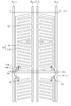
도 1은 본 발명의 실시예에 따른 인플레인 스위칭 모드 액정표시장치의 박막 트랜지스터 기판을 나타낸 평면도이며, 도 2는 도 1에 도시된 Ⅰ-Ⅰ’선에 따른 박막 트랜지스터 기판을 나타낸 단면도이다. FIG. 1 is a plan view of a thin film transistor substrate of an in-plane switching mode liquid crystal display according to an embodiment of the present invention, and FIG. 2 is a cross-sectional view of a thin film transistor substrate taken along a line I-I 'shown in FIG.
도 1 및 도 2에 도시된 인플레인 스위칭 모드 액정표시장치는 기판(100) 상에 형성된 복수의 게이트 라인(GL)과, 게이트 절연막(112)을 사이에 두고 게이트 라인(GL)과 교차하게 형성되어 화소 영역을 정의하는 복수의 데이터 라인(DL)과, 게이트 라인(GL) 및 데이터 라인(DL)이 교차하는 부분에 형성된 박막 트랜지스터(TFT)와, 박막 트랜지스터(TFT)와 접속되는 화소 전극(130)과, 각 화소 영역에서 화소 전극(130)과 수평 전계를 형성하는 공통 전극(140)과, 데이터 라인(DL) 사이에서 공통 전극(140)과 접속되어 형성되는 공통 라인(CL)을 포함한다. 여기서, 화소 전극(130)과 공통 전극(CL)은 가로 방향 러빙이 적용된 인플레인 스위칭 구조이다. The switching mode liquid crystal display of FIG. 1 and FIG. 2 includes a plurality of gate lines GL formed on a
게이트 라인(GL) 및 데이터 라인(DL)은 박막 트랜지스터 어레이 외곽부에서 구동 회로부와 접속된 패드 단자에 접속됨으로써 박막 트랜지스터(TFT)에 게이트 신호 및 데이터 신호를 공급한다. 제 2i(i는 자연수)번째 게이트 라인(GL2i)과 제 2i+1번째 게이트 라인(GL2i+1)은 서로 인접하도록 형성된다. The gate line GL and the data line DL are connected to a pad terminal connected to the driving circuit portion in the outer portion of the thin film transistor array to supply a gate signal and a data signal to the thin film transistor TFT. The second i-th gate line GL2i (i is a natural number) and the (2i + 1) -th gate line GL2i + 1 are formed adjacent to each other.
공통 라인(CL)은 데이터 라인(DL)들 사이에서 데이터 라인(DL)과 나란하게 형성되며, 기수번째 공통 라인(CL2k-1)(k는 자연수)과 우수번째 공통 라인(CL2k)이 서로 인접하도록 형성되어 액정을 구동하기 위한 기준 전압을 공통 전극(140)에 공급한다.The common line CL is formed in parallel with the data line DL between the data lines DL and the odd-numbered common line CL2k-1 (k is a natural number) and the even-numbered common line CL2k are adjacent to each other And supplies a reference voltage for driving the liquid crystal to the
공통 라인들(CL)을 사이에 두고 양측에 위치하는 액정셀들은 서로 다른 데이터 라인(DL)에 접속되고, 데이터 라인(DL)을 사이에 두고 양측에 위치하는 액정셀들은 데이터 라인(DL)을 공유한다. 여기서, 액정셀은 액정을 사이에 두고 마주보는 공통 전극(140) 및 화소 전극(130)을 의미한다. The liquid crystal cells located on both sides of the common lines CL are connected to different data lines DL and the liquid crystal cells located on both sides of the data line DL are connected to the data lines DL Share. Here, the liquid crystal cell means the
박막 트랜지스터(TFT)는 게이트 라인(GL)에서 분기된 게이트 전극(102)과, 게이트 전극(102)이 형성된 기판(100)의 전면에 형성된 게이트 절연막(112)과, 게이트 절연막(112) 상에 게이트 전극(102)과 중첩되게 형성된 오믹 콘택층(108a) 및 활성층(108b)으로 구성된 반도체층(108)과, 데이터 라인(DL)에서 분기되어 반도체층(108) 상에 형성되는 소스 전극(110a), 반도체층(108) 상에 소스 전극(110a)과 마주하게 형성된 드레인 전극(110b)으로 구성된다. The thin film transistor TFT includes a
화소 전극(130)은 데이터 라인(DL)과 평행하게 형성된 수직부(130a)와, 화소 전극(130)의 수직부(130a)에서 분기되어 게이트 라인(GL)과 나란하게 형성된 다수 의 핑거부(130b)를 포함한다. 화소 전극(130)의 핑거부(130b)들은 화소 영역의 중심부에서 서로 대칭되도록 경사되어 형성되며, 다수의 핑거부(130b) 중 최상단 및 최하단 핑거는 타 핑거부보다 상대적으로 두꺼운 폭으로 형성된다. 최하단 핑거는 보호막(120)을 관통하는 콘택홀(150)을 통해 드레인 전극(110b)과 접속된다. The
공통 전극(140)은 공통 라인(CL)에서 분기되어 화소 전극(130)의 핑거부(130b)와 교번되어 형성되어 수평 전계를 이룬다. 공통 전극(140)의 핑거부(140b)들은 화소 전극(130)의 핑거부(130b)와 같이 화소 영역의 중심부에서 서로 대칭되도록 경사되어 형성된다. The
화소 전극(130) 및 공통 전극(140)은 투명 도전층 또는 불투명 금속층으로 형성될 수 있다. 투명 도전층으로는 인듐주석산화물(Indium Tin Oxide : ITO), 주석산화물(Tin Oxide : TO), 인듐아연산화물(Indium Zinc Oxide : IZO) 또는 인듐주석아연산화물(Indium Tin Zinc Oxide : ITZO) 등이 이용된다. 불투명 금속층으로는 몰리브덴(Mo), 알루미늄(Al), 알루미늄-네오디미늄(Al-Nd), 구리(Cu), 크롬(Cr), 티타늄(Ti) 등의 금속과 이들의 합금이 단일층 또는 복수층 구조로 이용된다. The
기수번째 엑정셀과 우수번째 액정셀은 공통 라인(CL)을 기준으로 대칭되도록 형성 즉, 데이터 라인(DL), 화소 전극(130), 공통 라인(CL), 공통 라인(CL), 화소 전극(130), 데이터 라인(DL) 순서로 형성한다. 여기서, 데이터 라인(DL), 화소 전극(130), 공통 라인(CL), 화소 전극(130), 공통 라인(CL), 데이터 라인(DL) 순서로 형성하게 되면 기수번째 화소 영역의 화소 전극(130)과 데이터 라인(DL) 간의 커플 링 크기와 우수번째 화소 영역에서의 화소 전극(130)과 데이터 라인(DL)간의 커플링 크키가 다르게 되어 세로선 불량이 발생하게 되므로 이를 방지하기 위해서는 데이터 라인(DL)과 화소 전극(130) 간 일정 거리가 요구되므로 개구율이 감소되는 문제점이 있다. The odd-numbered liquid crystal cell and the odd-numbered liquid crystal cell are formed symmetrically with respect to the common line CL, ie, the data line DL, the
따라서, 기수번째 화소 영역과 우수번째 화소 영역에서의 데이터 라인(DL)과 화소 전극(130)은 공통 라인(CL)을 기준으로 대칭되도록 형성함으로써, 데이터 라인(DL)과 화소 전극(130) 간의 커플링 크기가 같게 되어 세로선 불량을 방지할 수 있다. 또한, 공통 라인(CL)을 공유함으로써 개구율을 향상시킬 수 있다. Therefore, the data lines DL and the
공통 라인(CL)은 도 3과 같이 기수번째 액정셀과 우수번째 액정셀이 서로 공유하도록 형성할 수도 있다. The common line CL may be formed such that the odd-numbered liquid crystal cell and the even-numbered liquid crystal cell share each other as shown in FIG.
도면에서는 생략하였으나, 박막 트랜지스터 기판(100)은 컬러필터 기판과 액정층을 사이에 두고 합착된다. 컬러필터 기판은 빛샘 방지 및 화소 영역을 구분하도록 형성된 블랙 매트릭스와, 컬러 색상을 표현하기 위한 컬러필터층을 포함한다. 여기서, 블랙 매트릭스는 박막 트랜지스터 기판(100)의 게이트 라인(GL) 및 데이터 라인(DL) 등과 같은 금속 패턴에 대응되도록 형성한다. Though not shown in the figure, the thin
상기와 같이, 데이터 라인들(DL) 사이에 공통 라인(CL)이 형성된 구조 즉, 도 1 및 도 3의 구조는 도 4a 내지 도 4d에 도시된 데이터 라인(DL)을 절감할 수 있는 구조에서도 적용 가능하다. As described above, the structure in which the common line CL is formed between the data lines DL, that is, the structure shown in FIGS. 1 and 3, can reduce the data line DL shown in FIGS. 4A to 4D Applicable.
도 4a 내지 도 4d는 데이터 라인(DL)을 절감할 수 있는 액정 패널의 제 1 및 제 4 실시예를 나타낸 회로도이다. 4A to 4D are circuit diagrams showing first and fourth embodiments of a liquid crystal panel capable of saving a data line DL.
도 4a는 박막 트랜지스터(TFT)가 S자로 배치되어 형성되며, 도 4b는 박막 트랜지스터(TFT)가 C자로 배치되어 형성되며, 도 4c는 박막 트랜지스터(TFT)가 역Z자로 배치되어 형성되며, 도 4d는 박막 트랜지스터(TFT)가 역S자로 배치되어 형성된다. 도 4a 내지 도 4d는 기수번째 데이터 라인(DLk-1)과 우수번째 데이터 라인(DL2k) 사이에 적어도 하나의 공통 라인(CL)이 형성되며, 우수번째 데이터 라인(DL2k)은 인접한 화소 영역과 공유하도록 형성된다. 즉, 데이터 라인(DL)을 액정셀 적어도 2개당 하나씩 형성하여 데이터 라인(DL) 및 데이터 드라이버 IC의 수 또한 절감시킬 수 있으며, 이에 따라 개구율을 향상시킬 수 있다. FIG. 4A is a cross-sectional view of a semiconductor device in which thin film transistors (TFTs) are arranged in an S-shape, FIG. 4B is a cross- And 4d are formed by disposing thin film transistors (TFTs) in an inverted S-shape. 4A to 4D show that at least one common line CL is formed between the odd-numbered data line DLk-1 and the even-numbered data line DL2k, and the even-numbered data line DL2k is shared with the adjacent pixel region. . That is, the number of the data lines DL and the number of the data driver ICs can be reduced by forming one data line DL per at least two liquid crystal cells, thereby improving the aperture ratio.
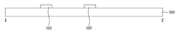
도 5은 본 발명의 다른 실시예에 따른 인플레인 스위칭 모드 액정표시장치의 박막 트랜지스터 기판(100)을 나타낸 평면도이며, 도 6는 도 5에 도시된 Ⅱ-Ⅱ’선에 따른 박막 트랜지스터 기판(100)을 나타낸 단면도이다. 5 is a plan view illustrating a thin
도 5 및 도 6에 도시된 인플레인 스위칭 모드 액정표시장치는 도 1 및 도 2와 대비하여 중복된 구성 요소들에 대한 설명은 생략하기로 한다. 5 and 6, the description of the redundant elements in the in-plane switching mode liquid crystal display device will be omitted in comparison with FIG. 1 and FIG.
도 5 및 도 6을 참조하면, 제 2i번째 게이트 라인(GL2i)에 접속된 박막 트랜지스터(TFT)와 제 2i+1번째 게이트 라인(GL2i+1)에 접속된 박막 트랜지스터(TFT)는 소스 전극(110a)을 공유하도록 형성된다. 소스 전극(110a)은 데이터 라인(DL)에서 분기되어 H자 형태로 형성된다. 5 and 6, the thin film transistor TFT connected to the second i-th gate line GL2i and the thin film transistor TFT connected to the (2i + 1) th gate line GL2i + 1 are connected to the
여기서, 박막 트랜지스터(TFT) 각각은 게이트 라인(GL)에서 분기된 게이트 전극(102)과, 게이트 전극(102)이 형성된 기판(100)의 전면에 형성된 게이트 절연막(112)과, 게이트 절연막(112) 상에 게이트 전극(102)과 중첩되게 형성된 오믹 콘 택층(108a) 및 활성층(108b)으로 구성된 반도체층(108)과, 데이터 라인(DL)에서 분기되어 반도체층(108) 상에 제 2i번째 게이트 라인(GL2i)과 제 2i+1번째 게이트 라인(GL2i+1)에 접속되어 형성되는 소스 전극(110a), 반도체층(108) 상에 소스 전극(110a)과 마주하게 형성된 드레인 전극(110b)으로 구성된다. Each of the thin film transistors TFT includes a
이와 같이, 상하로 인접한 액정셀이 소스 전극(110a)을 공유하도록 형성함으로써 개구율을 향상시킬 수 있다. 또한, 소스 전극(110a) 및 게이트 라인(GL)과의 중첩 면적이 종래에 비해 감소하게 되어 데이터 라인(DL)의 로딩 또한 작아지게 되어 데이터 라인(DL) 딜레이를 줄일 수 있다. In this manner, the aperture ratio can be improved by forming the liquid crystal cells vertically adjacent to each other to share the
상기와 같이, 상하로 인접한 액정셀이 소스 전극(110a)을 공유하는 구조는 도 4b 내지 도 4d의 데이터 라인(DL)을 절감할 수 있는 구조에서 마주보는 박막 트랜지스터(TFT)에서 적용가능 하다. As described above, the structure in which the upper and lower adjacent liquid crystal cells share the
도 7a 내지 도 7e는 도 5에 도시된 박막 트랜지스터 기판(100)의 제조방법을 나타낸 공정단면도들이다. 7A to 7E are process sectional views showing a method of manufacturing the thin
도 7a를 참조하면, 박막 트랜지스터 기판(100) 상에 게이트 라인(GL), 게이트 전극(102)을 포함하는 제 1 도전 패턴이 형성된다. Referring to FIG. 7A, a first conductive pattern including a gate line GL and a
구체적으로, 박막 트랜지스터 기판(100) 상에 게이트 금속층을 스퍼터링 등의 증착 방법으로 형성한다. 이어서, 마스크를 이용한 포토리쏘그래피 공정 및 식각 공정으로 택게이트 금속층이 패터닝하여 게이트 라인(GL) 및 게이트 전극(102)을 형성한다. Specifically, a gate metal layer is formed on the thin
게이트 금속층은 몰리브덴(Mo), 알루미늄(Al), 알루미늄-네오디미늄(Al-Nd), 구리(Cu), 크롬(Cr), 티타늄(Ti) 등의 금속과 이들의 합금이 단일층 또는 복수층 구조로 형성된다.The gate metal layer may be formed of a single layer or a plurality of layers of metals such as molybdenum (Mo), aluminum (Al), aluminum-neodymium (Al-Nd), copper (Cu), chromium (Cr), titanium Layer structure.
도 7b를 참조하면, 제 1 도전 패턴을 포함하는 기판(100) 상에 게이트 절연막(112), 반도체층(108)이 순차적으로 형성된다. Referring to FIG. 7B, a
구체적으로, 게이트 라인(GL), 게이트 전극(102) 및 공통 라인(145)을 포함하는 박막 트랜지스터 기판(100) 전면에 PECVD(Plasma Enhanced Chemical Vapor Deposition)등의 증착 방법으로 게이트 절연막(112), 비정질실리콘(a-Si)층 및 불순물(n+)이 도핑된 비정질실리콘층이 순차적으로 형성된다. 이어서, 마스크를 이용한 포토리쏘그래피 공정 및 식각 공정에 의해 패터닝되어 활성층(108b) 및 오믹 콘택층(108a)으로 구성된 반도체층(108)이 형성된다. Specifically, a
게이트 절연막(112)은 산화 실리콘(SiOx) 또는 질화 실리콘(SiNx) 등의 무기 절연물질이 이용된다. As the
도 7c를 참조하면, 반도체층(108) 상에 데이터 라인(DL), 소스 및 드레인 전극(110a, 110b)을 포함하는 소스/드레인 패턴이 형성된다. Referring to FIG. 7C, a source / drain pattern including a data line DL, source and
구체적으로, 반도체층(108)을 포함하는 기판(100) 상에 소스/드레인 금속층을 스퍼터링 등의 증착 방법으로 형성한 후, 데이터 라인(DL), 소스 및 드레인 전극(110a, 110b)을 포함하는 소스/드레인 패턴이 순차적으로 형성된다. 이때, 소스 및 드레인 전극(110a, 110b)과 오믹 콘택층(108a)의 전기적인 분리를 위해 회절 노광 또는 하프톤 마스크(half-tone mask)가 이용된다. 여기서, 소스 전극(110a)은 상하로 인접한 액정셀 즉, 도 5의 제 2i번째 게이트 라인(GL2i)에 접속된 박막 트 랜지스터(TFT)와 제 2i+1번째 게이트 라인(GL2i+1)에 접속된 박막 트랜지스터(TFT)가 서로 공유하도록 형성된다. Specifically, after a source / drain metal layer is formed on a
소스/드레인 금속층은 몰리브덴(Mo), 알루미늄(Al), 알루미늄-네오디미늄(Al-Nd), 구리(Cu), 크롬(Cr), 티타늄(Ti), 몰리티타늄 합금(MoTi), 몰리니오븀 합금(MoNb), 타이아늄니오븀 합금(TiNb) 등의 금속과 이들의 합금이 단일층 또는 복수층 구조로 형성된다. The source / drain metal layer may comprise at least one of Mo, Al, Al-Nd, Cu, Cr, Ti, MoTi, (MoNb), and a titanium-niobium alloy (TiNb), and alloys thereof are formed in a single-layer or multi-layer structure.
도 7d를 참조하면, 소스/드레인 패턴 상에 콘택홀(150)을 포함하는 보호막(120)이 형성된다. Referring to FIG. 7D, a
구체적으로, 데이터 라인(DL), 소스 및 드레인 전극(110a, 110b)을 포함하는 소스/드레인 패턴 상에 보호막(120)이 형성된다. 이어서, 보호막(120) 상에 마스크를 이용한 포토리쏘그래피 공정 및 식각 공정에 의해 패터닝되어 드레인 전극(110b)을 노출시키는 콘택홀(150)이 형성된다. Specifically, the
보호막(120)은 게이트 절연막(112)과 같은 무기 절연물질이 PECVD 등의 증착 방법으로 증착되어 형성되거나, 유전상수가 작은 아크릴(acryl)계 유기화합물, BCB(Benzocyclobuten), PFCB(Perfluorocyclobutane), 테프론(teflon), 사이토프(Cytop) 등과 같은 유기 절연물질이 스핀 또는 스핀리스 등의 코팅 방법으로 코팅되어 형성된다. The
도 7e를 참조하면, 보호막(120) 상에 공통 라인(CL), 화소 전극(130) 및 공통 전극(140)이 형성된다. Referring to FIG. 7E, a common line CL, a
구체적으로, 보호막(120) 상에 투명 도전 물질을 증착한 후 마스크를 이용한 포토리쏘그래피 공정 및 식각 공정에 의해 패터닝되어 공통 라인(CL)과, 콘택홀(150)을 통해 드레인 전극(110b)과 전기적으로 접속되는 화소 전극(130)과, 공통 라인(CL)과 전기적으로 접속되어 화소 전극(130)과 수평 전계를 이루는 공통 전극(140)이 형성된다. Specifically, a transparent conductive material is deposited on the
여기서, 공통 라인(CL), 화소 전극(130) 및 공통 전극(140)은 불투명 금속층으로 형성될 수 있다. 투명 도전층으로는 인듐주석산화물(Indium Tin Oxide : ITO), 주석산화물(Tin Oxide : TO), 인듐아연산화물(Indium Zinc Oxide : IZO) 또는 인듐주석아연산화물(Indium Tin Zinc Oxide : ITZO) 등이 이용된다. 불투명 금속층으로는 몰리브덴(Mo), 알루미늄(Al), 알루미늄-네오디미늄(Al-Nd), 구리(Cu), 크롬(Cr), 티타늄(Ti) 등의 금속과 이들의 합금이 단일층 또는 복수층 구조로 이용된다. Here, the common line CL, the
이와 같이, 상하로 인접한 액정셀과 서로 공유하도록 형성된 소스 전극(110a)이 형성된 구조는 도 8a 및 도 8b와 같이 공통 라인(CL)을 기수번째 액정셀과 우수번째 액정셀이 공유하도록 형성된 구조에서도 적용 가능하며, 인플레인 스위칭 모드의 액정표시장치에 한정되지 않는다. The structure in which the
상하로 인접한 액정셀과 서로 공유하도록 형성된 소스 전극(110a)이 형성된 구조는 도 9a 및 도 9b와 같이 소스 전극(110a)을 역E자 형태로 형성할 수도 있다. The
이때, 역E자의 소스 전극(110a)의 중앙 부분은 상하로 인접한 액정셀의 제 2i번째 게이트 라인(GL2i) 및 제 2i+1번째 게이트 라인(GL2i+1) 사이에서 위치하며, 제 2i번째 게이트 라인(GL2i) 및 제 2i+1번째 게이트 라인(GL2i+1)에 중첩되도 록 형성할 수도 있다. At this time, the central portion of the
이상에서 설명한 본 발명은 상술한 실시예 및 첨부된 도면에 한정되는 것이 아니고, 본 발명의 기술적 사상을 벗어나지 않는 범위 내에서 여러 가지 치환, 변형 및 변경 가능하다는 것이 본 발명이 속하는 기술분야에서 통상의 지식을 가진 자에게 있어 명백할 것이다. It will be apparent to those skilled in the art that various modifications and variations can be made in the present invention without departing from the spirit or scope of the invention. It will be clear to those who have knowledge.
도 1 본 발명의 실시예에 따른 인플레인 스위칭 모드 액정표시장치의 박막 트랜지스터 기판을 나타낸 평면도이다.1 is a plan view of a thin film transistor substrate of an in-plane switching mode liquid crystal display according to an embodiment of the present invention.
도 2는 도 1에 도시된 Ⅰ-Ⅰ’선에 따른 박막 트랜지스터 기판을 나타낸 단면도이다. 2 is a cross-sectional view of the thin film transistor substrate taken along the line I-I 'shown in FIG.
도 3은 본 발명의 다른 실시예에 따른 인플레인 스위칭 모드 액정표시장치의 박막 트랜지스터 기판을 나타낸 평면도이다.3 is a plan view of a thin film transistor substrate of an in-plane switching mode liquid crystal display according to another embodiment of the present invention.
도 4a 내지 도 4d는 데이터 라인을 절감할 수 있는 액정 패널의 제 1 및 제 4 실시예를 나타낸 회로도이다.4A to 4D are circuit diagrams showing first and fourth embodiments of a liquid crystal panel capable of saving data lines.
도 5은 본 발명의 또 다른 실시예에 따른 인플레인 스위칭 모드 액정표시장치의 박막 트랜지스터 기판을 나타낸 평면도이다.5 is a plan view of a thin film transistor substrate of an in-plane switching mode liquid crystal display according to another embodiment of the present invention.
도 6는 도 5에 도시된 Ⅱ-Ⅱ’선에 따른 박막 트랜지스터 기판을 나타낸 단면도이다. 6 is a cross-sectional view of the thin film transistor substrate taken along a line II-II 'shown in FIG.
도 7a 내지 도 7e는 도 5에 도시된 박막 트랜지스터 기판의 제조방법을 나타낸 공정단면도들이다.FIGS. 7A to 7E are process sectional views showing a method of manufacturing the thin film transistor substrate shown in FIG.
도 8a 및 도 8b는 기수번째 액정셀과 우수번째 액정셀이 공통 라인을 공유하도록 형성된 인플레인 스위칭 모드 액정표시장치의 박막 트랜지스터 기판을 나타낸 도면이다.8A and 8B are views showing a thin film transistor substrate of a switching mode liquid crystal display device in which an odd-numbered liquid crystal cell and an even-numbered liquid crystal cell are formed to share a common line.
도 9a 및 도 9b는 상하로 인접한 액정셀과 서로 공유하도록 형성된 소스 전극을 구비하는 박막 트랜지스터기판을 나타낸 도면이다. FIGS. 9A and 9B are diagrams showing a thin film transistor substrate having a source electrode formed so as to be in common with upper and lower adjacent liquid crystal cells. FIG.
< 도면의 주요 부분에 대한 부호의 설명 >Description of the Related Art
GL : 게이트 라인 DL : 데이터 라인GL: gate line DL: data line
CL : 공통 라인 100 : 박막 트랜지스터 기판CL: common line 100: thin film transistor substrate
102 : 게이트 전극 108 : 반도체층102: gate electrode 108: semiconductor layer
110a, 110b : 소스 및 드레인 전극 112 : 게이트 절연막110a, 110b: source and drain electrodes 112: gate insulating film
120 : 보호막 130 : 화소 전극120: protective film 130: pixel electrode
140 : 공통 전극 150 : 콘택홀140: common electrode 150: contact hole
Claims (7)
Priority Applications (1)
| Application Number | Priority Date | Filing Date | Title |
|---|---|---|---|
| KR1020080037465A KR101429921B1 (en) | 2008-04-22 | 2008-04-22 | Liquid crystal display device |
Applications Claiming Priority (1)
| Application Number | Priority Date | Filing Date | Title |
|---|---|---|---|
| KR1020080037465A KR101429921B1 (en) | 2008-04-22 | 2008-04-22 | Liquid crystal display device |
Publications (2)
| Publication Number | Publication Date |
|---|---|
| KR20090111730A KR20090111730A (en) | 2009-10-27 |
| KR101429921B1 true KR101429921B1 (en) | 2014-08-13 |
Family
ID=41539467
Family Applications (1)
| Application Number | Title | Priority Date | Filing Date |
|---|---|---|---|
| KR1020080037465A Active KR101429921B1 (en) | 2008-04-22 | 2008-04-22 | Liquid crystal display device |
Country Status (1)
| Country | Link |
|---|---|
| KR (1) | KR101429921B1 (en) |
Families Citing this family (2)
| Publication number | Priority date | Publication date | Assignee | Title |
|---|---|---|---|---|
| KR101830274B1 (en) | 2011-01-28 | 2018-02-21 | 삼성디스플레이 주식회사 | Liquid crystal display |
| KR101922088B1 (en) * | 2012-05-23 | 2018-11-27 | 삼성디스플레이 주식회사 | Liquid crystal display |
Citations (4)
| Publication number | Priority date | Publication date | Assignee | Title |
|---|---|---|---|---|
| KR20050045471A (en) * | 2003-11-11 | 2005-05-17 | 엘지.필립스 엘시디 주식회사 | In plane switching mode liquid crystal display device and method for fabricating thereof |
| KR20050111967A (en) * | 2004-05-24 | 2005-11-29 | 엘지.필립스 엘시디 주식회사 | An array substrate for in-plane switching mode lcd |
| KR20060011295A (en) * | 2004-07-30 | 2006-02-03 | 주식회사 뉴인텍 | Deposition film for metallized film capacitor and manufacturing method thereof |
| KR20070080143A (en) * | 2006-02-06 | 2007-08-09 | 엘지.필립스 엘시디 주식회사 | LCD Display |
-
2008
- 2008-04-22 KR KR1020080037465A patent/KR101429921B1/en active Active
Patent Citations (4)
| Publication number | Priority date | Publication date | Assignee | Title |
|---|---|---|---|---|
| KR20050045471A (en) * | 2003-11-11 | 2005-05-17 | 엘지.필립스 엘시디 주식회사 | In plane switching mode liquid crystal display device and method for fabricating thereof |
| KR20050111967A (en) * | 2004-05-24 | 2005-11-29 | 엘지.필립스 엘시디 주식회사 | An array substrate for in-plane switching mode lcd |
| KR20060011295A (en) * | 2004-07-30 | 2006-02-03 | 주식회사 뉴인텍 | Deposition film for metallized film capacitor and manufacturing method thereof |
| KR20070080143A (en) * | 2006-02-06 | 2007-08-09 | 엘지.필립스 엘시디 주식회사 | LCD Display |
Also Published As
| Publication number | Publication date |
|---|---|
| KR20090111730A (en) | 2009-10-27 |
Similar Documents
| Publication | Publication Date | Title |
|---|---|---|
| JP4881368B2 (en) | Manufacturing method of liquid crystal display device | |
| US8519396B2 (en) | Array substrate for in-plane switching mode liquid crystal display device and fabricating method thereof | |
| JP5329169B2 (en) | Thin film transistor substrate and liquid crystal display device including the same | |
| US7978294B2 (en) | Liquid crystal display device | |
| US20080180623A1 (en) | Liquid crystal display device | |
| US7061566B2 (en) | In-plane switching mode liquid crystal display device and method of fabricating the same | |
| US20070285591A1 (en) | Liquid crystal display panel and method of manufacturing the same | |
| US8451410B2 (en) | Array substrate for wide viewing angle liquid crystal display device and mehod of manufacturing the same | |
| KR20080100692A (en) | LCD and its manufacturing method | |
| US20080143907A1 (en) | Liquid crystal display device and method of manufacturing the same | |
| KR101429921B1 (en) | Liquid crystal display device | |
| US7863613B2 (en) | Thin film transistor array of horizontal electronic field applying type and method for fabricating the same | |
| US20160155753A1 (en) | Display device | |
| KR101970550B1 (en) | Thin film transistor substrate and method of fabricating the same | |
| KR100512623B1 (en) | array circuit board of LCD and fabrication method of thereof | |
| KR101107685B1 (en) | Transverse electric field liquid crystal display device and manufacturing method thereof | |
| KR101429919B1 (en) | A liquid crystal display device of an in-plane switching mode | |
| KR101668993B1 (en) | In Plane Switching mode Liquid Crystal Display Device | |
| KR101136207B1 (en) | Thin film transistor array substrate and fabricating method thereof | |
| KR20120035364A (en) | In-plane switching mode lcd and method of manufacturing the same | |
| KR101267532B1 (en) | The Liquid Crystal Display Device of a storage on common type and the method for fabricating thereof | |
| KR20090070174A (en) | LCD panel and manufacturing method | |
| KR20130103022A (en) | Thin film transistor substrate and method of fabricating the same | |
| KR20080040478A (en) | Liquid crystal display panel and manufacturing method thereof | |
| KR20080099597A (en) | In-plane switching mode liquid crystal display device and manufacturing method thereof |
Legal Events
| Date | Code | Title | Description |
|---|---|---|---|
| PA0109 | Patent application |
St.27 status event code: A-0-1-A10-A12-nap-PA0109 |
|
| PG1501 | Laying open of application |
St.27 status event code: A-1-1-Q10-Q12-nap-PG1501 |
|
| R18-X000 | Changes to party contact information recorded |
St.27 status event code: A-3-3-R10-R18-oth-X000 |
|
| R18-X000 | Changes to party contact information recorded |
St.27 status event code: A-3-3-R10-R18-oth-X000 |
|
| R18-X000 | Changes to party contact information recorded |
St.27 status event code: A-3-3-R10-R18-oth-X000 |
|
| A201 | Request for examination | ||
| PA0201 | Request for examination |
St.27 status event code: A-1-2-D10-D11-exm-PA0201 |
|
| D13-X000 | Search requested |
St.27 status event code: A-1-2-D10-D13-srh-X000 |
|
| D14-X000 | Search report completed |
St.27 status event code: A-1-2-D10-D14-srh-X000 |
|
| E902 | Notification of reason for refusal | ||
| PE0902 | Notice of grounds for rejection |
St.27 status event code: A-1-2-D10-D21-exm-PE0902 |
|
| E13-X000 | Pre-grant limitation requested |
St.27 status event code: A-2-3-E10-E13-lim-X000 |
|
| P11-X000 | Amendment of application requested |
St.27 status event code: A-2-2-P10-P11-nap-X000 |
|
| P13-X000 | Application amended |
St.27 status event code: A-2-2-P10-P13-nap-X000 |
|
| E701 | Decision to grant or registration of patent right | ||
| PE0701 | Decision of registration |
St.27 status event code: A-1-2-D10-D22-exm-PE0701 |
|
| GRNT | Written decision to grant | ||
| PR0701 | Registration of establishment |
St.27 status event code: A-2-4-F10-F11-exm-PR0701 |
|
| PR1002 | Payment of registration fee |
St.27 status event code: A-2-2-U10-U11-oth-PR1002 Fee payment year number: 1 |
|
| PG1601 | Publication of registration |
St.27 status event code: A-4-4-Q10-Q13-nap-PG1601 |
|
| P22-X000 | Classification modified |
St.27 status event code: A-4-4-P10-P22-nap-X000 |
|
| FPAY | Annual fee payment |
Payment date: 20170713 Year of fee payment: 4 |
|
| PR1001 | Payment of annual fee |
St.27 status event code: A-4-4-U10-U11-oth-PR1001 Fee payment year number: 4 |
|
| PR1001 | Payment of annual fee |
St.27 status event code: A-4-4-U10-U11-oth-PR1001 Fee payment year number: 5 |
|
| PR1001 | Payment of annual fee |
St.27 status event code: A-4-4-U10-U11-oth-PR1001 Fee payment year number: 6 |
|
| PR1001 | Payment of annual fee |
St.27 status event code: A-4-4-U10-U11-oth-PR1001 Fee payment year number: 7 |
|
| PR1001 | Payment of annual fee |
St.27 status event code: A-4-4-U10-U11-oth-PR1001 Fee payment year number: 8 |
|
| PR1001 | Payment of annual fee |
St.27 status event code: A-4-4-U10-U11-oth-PR1001 Fee payment year number: 9 |
|
| PR1001 | Payment of annual fee |
St.27 status event code: A-4-4-U10-U11-oth-PR1001 Fee payment year number: 10 |
|
| PR1001 | Payment of annual fee |
St.27 status event code: A-4-4-U10-U11-oth-PR1001 Fee payment year number: 11 |
|
| P22-X000 | Classification modified |
St.27 status event code: A-4-4-P10-P22-nap-X000 |
|
| PR1001 | Payment of annual fee |
St.27 status event code: A-4-4-U10-U11-oth-PR1001 Fee payment year number: 12 |
|
| U11 | Full renewal or maintenance fee paid |
Free format text: ST27 STATUS EVENT CODE: A-4-4-U10-U11-OTH-PR1001 (AS PROVIDED BY THE NATIONAL OFFICE) Year of fee payment: 12 |