KR101334844B1 - Single poly eeprom and method for fabricating the same - Google Patents
Single poly eeprom and method for fabricating the same Download PDFInfo
- Publication number
- KR101334844B1 KR101334844B1 KR1020110146422A KR20110146422A KR101334844B1 KR 101334844 B1 KR101334844 B1 KR 101334844B1 KR 1020110146422 A KR1020110146422 A KR 1020110146422A KR 20110146422 A KR20110146422 A KR 20110146422A KR 101334844 B1 KR101334844 B1 KR 101334844B1
- Authority
- KR
- South Korea
- Prior art keywords
- conductivity type
- floating gate
- type impurity
- region
- impurity region
- Prior art date
- Legal status (The legal status is an assumption and is not a legal conclusion. Google has not performed a legal analysis and makes no representation as to the accuracy of the status listed.)
- Expired - Fee Related
Links
Images


Classifications
-
- G—PHYSICS
- G11—INFORMATION STORAGE
- G11C—STATIC STORES
- G11C16/00—Erasable programmable read-only memories
- G11C16/02—Erasable programmable read-only memories electrically programmable
- G11C16/04—Erasable programmable read-only memories electrically programmable using variable threshold transistors, e.g. FAMOS
- G11C16/0408—Erasable programmable read-only memories electrically programmable using variable threshold transistors, e.g. FAMOS comprising cells containing floating gate transistors
- G11C16/0441—Erasable programmable read-only memories electrically programmable using variable threshold transistors, e.g. FAMOS comprising cells containing floating gate transistors comprising cells containing multiple floating gate devices, e.g. separate read-and-write FAMOS transistors with connected floating gates
-
- H—ELECTRICITY
- H10—SEMICONDUCTOR DEVICES; ELECTRIC SOLID-STATE DEVICES NOT OTHERWISE PROVIDED FOR
- H10B—ELECTRONIC MEMORY DEVICES
- H10B41/00—Electrically erasable-and-programmable ROM [EEPROM] devices comprising floating gates
- H10B41/60—Electrically erasable-and-programmable ROM [EEPROM] devices comprising floating gates the control gate being a doped region, e.g. single-poly memory cell
-
- H—ELECTRICITY
- H10—SEMICONDUCTOR DEVICES; ELECTRIC SOLID-STATE DEVICES NOT OTHERWISE PROVIDED FOR
- H10D—INORGANIC ELECTRIC SEMICONDUCTOR DEVICES
- H10D30/00—Field-effect transistors [FET]
- H10D30/60—Insulated-gate field-effect transistors [IGFET]
- H10D30/68—Floating-gate IGFETs
- H10D30/681—Floating-gate IGFETs having only two programming levels
- H10D30/684—Floating-gate IGFETs having only two programming levels programmed by hot carrier injection
-
- H—ELECTRICITY
- H10—SEMICONDUCTOR DEVICES; ELECTRIC SOLID-STATE DEVICES NOT OTHERWISE PROVIDED FOR
- H10D—INORGANIC ELECTRIC SEMICONDUCTOR DEVICES
- H10D64/00—Electrodes of devices having potential barriers
- H10D64/01—Manufacture or treatment
- H10D64/031—Manufacture or treatment of data-storage electrodes
- H10D64/035—Manufacture or treatment of data-storage electrodes comprising conductor-insulator-conductor-insulator-semiconductor structures
-
- H—ELECTRICITY
- H10—SEMICONDUCTOR DEVICES; ELECTRIC SOLID-STATE DEVICES NOT OTHERWISE PROVIDED FOR
- H10D—INORGANIC ELECTRIC SEMICONDUCTOR DEVICES
- H10D84/00—Integrated devices formed in or on semiconductor substrates that comprise only semiconducting layers, e.g. on Si wafers or on GaAs-on-Si wafers
- H10D84/01—Manufacture or treatment
- H10D84/0123—Integrating together multiple components covered by H10D12/00 or H10D30/00, e.g. integrating multiple IGBTs
- H10D84/0126—Integrating together multiple components covered by H10D12/00 or H10D30/00, e.g. integrating multiple IGBTs the components including insulated gates, e.g. IGFETs
- H10D84/0165—Integrating together multiple components covered by H10D12/00 or H10D30/00, e.g. integrating multiple IGBTs the components including insulated gates, e.g. IGFETs the components including complementary IGFETs, e.g. CMOS devices
- H10D84/0191—Manufacturing their doped wells
-
- G—PHYSICS
- G11—INFORMATION STORAGE
- G11C—STATIC STORES
- G11C2216/00—Indexing scheme relating to G11C16/00 and subgroups, for features not directly covered by these groups
- G11C2216/02—Structural aspects of erasable programmable read-only memories
- G11C2216/10—Floating gate memory cells with a single polysilicon layer
Landscapes
- Engineering & Computer Science (AREA)
- Microelectronics & Electronic Packaging (AREA)
- Non-Volatile Memory (AREA)
- Semiconductor Memories (AREA)
Abstract
본 발명은 셀 밀도를 증가시킬 수 있을 뿐만 아니라 동작 전압을 낮출 수 있는 싱글 폴리형 이이피롬과 그 제조 방법에 관한 것이다.
이를 위하여 본 발명의 실시 예에 따른 싱글 폴리형 이이피롬은 반도체 기판 상에 형성된 제 2 도전형 웰과, 제 2 도전형 웰의 내부에 형성된 제 1 도전형의 소스 및 드레인 영역과, 제 2 도전형 웰의 상부에 형성된 터널 산화막과, 터널 산화막 상부에 형성되며, 제 2 도전형 불순물 이온이 도핑된 플로팅 게이트와, 플로팅 게이트와 인접한 제 2 도전형 웰의 내부에 형성된 제 1 도전형의 불순물 영역을 포함하며, 플로팅 게이트는, 드레인 영역과 인접한 부분의 농도가 불순물 영역과 인접한 부분 보다 높은 것을 특징으로 한다.The present invention relates to a single poly-type ypyrom and a method for manufacturing the same that can increase the cell density as well as lower the operating voltage.
To this end, a single poly-type ypyrom according to an embodiment of the present invention includes a second conductive well formed on a semiconductor substrate, a source and drain region of a first conductive type formed in the second conductive well, and a second conductive type. A tunnel oxide film formed over the well, a floating gate formed over the tunnel oxide film and doped with the second conductivity type impurity ions, and an impurity region of the first conductivity type formed inside the second conductivity type well adjacent to the floating gate. And a floating gate, wherein the concentration of the portion adjacent to the drain region is higher than the portion adjacent to the impurity region.
Description
본 발명은 반도체 메모리 셀에 관한 것으로, 더욱 상세하게는 셀 밀도를 증가시킬 수 있을 뿐만 아니라 동작 전압을 낮출 수 있는 싱글 폴리형 이이피롬과 그 제조 방법에 관한 것이다.
BACKGROUND OF THE INVENTION 1. Field of the Invention The present invention relates to a semiconductor memory cell, and more particularly, to a single polytype ypyrom and a method of manufacturing the same, which can increase cell density and lower operating voltage.
EEPROM(Electrically Erasable Programmable Read Only Memory)은 전기적으로 소거와 쓰기가 가능하며 전원 전압이 오프 되어도 데이터가 보존된다. 터널링(Tunneling)을 이용하여 전기적으로 소거(Erase)와 프로그래밍(Programming)이 가능하기 때문에 사용자가 정보 변경이 가능하다. 그러나, 2개의 트랜지스터로써 1셀(cell)을 구성해야 하기 때문에 EPROM에 비하여 면적이 크고 고가이다.EEPROM (Electrically Erasable Programmable Read Only Memory) can be electrically erased and written, and data is preserved even when the power supply voltage is turned off. Tunneling can be used to electrically erase and program, allowing the user to change information. However, the area is larger and more expensive than EPROM because one cell must be composed of two transistors.
일반적으로 비휘발성(non volatile) 메모리는 전원이 중단되어도 저장된 데이터가 손실되지 않는 장점이 있어 PC 바이오스(BIOS)용, 셋탑박스(Set top Box), 프린터(printer) 및 네트워크 서버(network server) 등의 데이터 저장용으로 많이 사용되고 있으며 최근에는 디지털 카메라와 휴대폰 등에서도 많이 이용되고 있는 실정이다.In general, non-volatile memory has the advantage that the stored data is not lost even if the power is interrupted. For PC BIOS, set top box, printer and network server, etc. It is widely used for data storage, and recently, it is also widely used in digital cameras and mobile phones.
이하, 첨부된 도면을 참조하여 종래의 단일 폴리(single poly) EEPROM 소자에 대해 설명한다.Hereinafter, a conventional single poly EEPROM device will be described with reference to the accompanying drawings.
먼저, 도 1a는 "channel hot electron injection" 방식으로 프로그램(Program)하는 방식을 나타낸 것으로, N-웰(Well)에 인가된 프로그램 전압(program voltage)(+Vp)에 의해 플로팅 게이트(floating gate)에 특정 전압이 유기되며(플로팅 게이트에 유기되는 전압은 커플링 비율(coupling ratio)에 의해 정해짐), 플로팅 게이트에 유기된 특정 전압에 의해 NMOS의 채널 영역을 반전시키게 된다.First, FIG. 1A illustrates a method of programming in a "channel hot electron injection" method, and a floating gate by a program voltage (+ Vp) applied to an N-well. The specific voltage is induced at (the voltage induced at the floating gate is determined by the coupling ratio), and the specific voltage induced at the floating gate inverts the channel region of the NMOS.
그리고, NMOS의 드레인(drain) 영역에 특정 전압(VDS)를 인가하면, 드레인에서 소스(source)쪽으로 전류가 흐르게 되며, 드레인 접합 영역 부근에서 발생되는 "channel hot electron"이 플로팅 게이트로 주입됨으로써 NMOS 소자의 문턱전압이 높아지게 된다.When a specific voltage VDS is applied to the drain region of the NMOS, a current flows from the drain to the source, and “channel hot electrons” generated near the drain junction region are injected into the floating gate so that the NMOS is injected. The threshold voltage of the device becomes high.
도 1b는 종래의 F/N 터널링(tunneling) 방식으로 소거(erase)하는 방식을 나타낸 것으로, N-웰은 접지(ground)시키고 NMOS 영역의 소스/드레인에 소거 전압(erase voltage)(+VE)를 인가한다.FIG. 1B illustrates a conventional method of erasing by F / N tunneling, where the N-well is grounded and an erase voltage (+ VE) is applied to the source / drain of the NMOS region. Apply.
상기와 같이 N-웰에 인가된 접지전압에 의해 플로팅 게이트에는 거의 접지전압에 가까운 전위(potential)이 유기되고, NMOS 영역의 소스/드레인에 인가된 소거 전압(+VE)에 의해 전기장(electric field)가 NMOS 소스/드레인에서 플로팅 게이트쪽으로 강하게 걸리게 된다.As described above, a potential close to the ground voltage is induced in the floating gate by the ground voltage applied to the N-well, and an electric field is generated by the erase voltage (+ VE) applied to the source / drain of the NMOS region. ) Is strongly caught on the floating gate from the NMOS source / drain.
상기와 같이 인가된 전기장에 의해 플로팅 게이트에 존재하는 전자들이 F/N 터널링하여 소스/드레인 영역으로 빠져나감으로써 NMOS 소자의 문턱전압이 낮아지게 된다.The electrons present in the floating gate are exited to the source / drain region by F / N tunneling by the applied electric field, thereby lowering the threshold voltage of the NMOS device.
도면 1c는 종래 EEPROM의 읽기(reading) 방식을 나타낸 것으로, N-웰에는 읽기 전압(reading voltage)(+VR)을 인가하며 이로 인해 플로팅 게이트에는 특정 전압이 유기되며, NMOS 소자의 드레인에는 읽기를 위한 포지티브 드레인 전압(positive drain voltage)를 인가하고 소스는 접지시키게 된다.FIG. 1C illustrates a reading method of a conventional EEPROM. A reading voltage (+ VR) is applied to an N-well, which causes a specific voltage to be induced in the floating gate, and a read in the drain of the NMOS device. Positive drain voltage is applied and the source is grounded.
만약, 플로팅 게이트에 전자가 주입되어 있는 프로그래밍 상태로 NMOS 소자의 문턱전압이 매우 높은 상태이면, 플로팅 게이트에 유기된 특정 전압으로도 NMOS 소자를 턴-온(turn-on) 시킬 수 없어 전류가 흐르지 않게 되며, 플로팅 게이트에 전자가 없는 소거 상태라면, NMOS 소자의 문턱전압이 매우 낮은 상태로 플로팅 게이트에 유기된 특정 전압으로도 NMOS 소자를 턴-온 시킬 수 있어 전류가 흐르게 된다.If the threshold voltage of the NMOS device is very high due to a programming state in which electrons are injected into the floating gate, current cannot flow because the specific voltage induced in the floating gate cannot turn on the NMOS device. In the erased state in which there is no electron in the floating gate, the NMOS device can be turned on even with a specific voltage induced in the floating gate while the threshold voltage of the NMOS device is very low, so that current flows.
상기와 같은 EEPROM 소자에 있어서 플로팅 게이트과 N-웰 사이에는 터널 산화막이 형성되며, 이러한 터널 산화막을 이용하여 드레인 접합 영역 부근에서 발생되는 "channel hot electron"을 트랩하게 된다. In the above EEPROM device, a tunnel oxide film is formed between the floating gate and the N-well, and the tunnel oxide film is used to trap "channel hot electrons" generated near the drain junction region.
그러나, 이와 같이 터널 산화막을 이용하는 방법은 소스에서 드레인쪽으로 걸리는 전압보다 높은 전압을 플로팅 게이트에 인가해야 하기 때문에 다른 소자에 영향을 줄 수 있는 단점이 있다. 이런 이유로, 플로팅 게이트에 충분한 전압을 인가하지 못하게 되기 때문에 소자의 신뢰성을 떨어뜨리는 요인이 되고 있다.However, the method using the tunnel oxide film as described above has a disadvantage in that it may affect other devices because a voltage higher than the voltage applied from the source to the drain must be applied to the floating gate. For this reason, since it is impossible to apply a sufficient voltage to the floating gate, it becomes a factor that reduces the reliability of the device.
또한, 종래의 단일 폴리 EEPROM 셀 경우, 프로그램/소거/읽기 동작을 위해 플로팅 게이트에 특정 전위를 유기시키기 위해 N-웰을 형성시켜야 하기 때문에 단위 셀 면적이 매우 커서 고밀도(high density)를 갖는 EEPROM을 구현하기가 어렵다.
In addition, in the conventional single poly EEPROM cell, since the N-well has to be formed in order to induce a specific potential in the floating gate for program / erase / read operations, an EEPROM having a high density due to a large unit cell area is required. Difficult to implement
상기와 같은 문제점을 해결하기 위해 안출된 것으로서, 본 발명의 목적은 플로팅 게이트의 하부에 형성되는 터널 산화막을 서로 다른 두께로 형성함으로써, 셀 밀도를 증가시킬 수 있는 싱글 폴리형 이이피롬과 그 제조 방법을 제공하는데 있다.The present invention has been made to solve the above problems, and an object of the present invention is to form a single polytype ypyrom and a method for manufacturing the same, by forming tunnel oxide films formed under the floating gates at different thicknesses, thereby increasing cell density. To provide.
또한, 본 발명은 플로팅 게이트의 일부 영역에 식각된 패턴을 형성함으로써, 전계 밀집 현상을 유발시켜 동작 전압을 낮출 수 있는 싱글 폴리형 이이피롬과 그 제조 방법을 제공하는데 있다.In addition, the present invention is to provide a single poly-type ypyrom and a method of manufacturing the same by forming an etched pattern in a portion of the floating gate, which can cause an electric field density phenomenon to lower the operating voltage.
또한, 본 발명은 서로 다른 도전형 불순물 농도 분포를 갖는 플로팅 게이트를 제공함으로써, 플로팅 게이트의 일함수(workfunction) 차이를 이용하여 동작 전압 차이를 유발시킬 수 있는 싱글 폴리형 이이피롬과 그 제조 방법을 제공하는데 있다.In addition, the present invention provides a single poly-type ypyrom and a method of manufacturing the same, which can cause a difference in operating voltage by using a floating gate work function difference by providing a floating gate having a different conductivity type impurity concentration distribution. To provide.
본 발명의 목적은 이상에서 언급한 목적으로 제한되지 않으며, 언급되지 않은 또 다른 목적들은 아래의 기재로부터 본 발명이 속하는 통상의 지식을 가진 자에게 명확하게 이해될 수 있을 것이다.
The objects of the present invention are not limited to the above-mentioned objects, and other objects not mentioned can be clearly understood by those skilled in the art from the following description.
본 발명의 일 측면에 따르면, 본 발명의 실시 예에 따른 싱글 폴리형 이이피롬은 반도체 기판 상에 형성된 제 2 도전형 웰과, 상기 제 2 도전형 웰의 내부에 형성된 제 1 도전형의 소스 및 드레인 영역과, 상기 제 2 도전형 웰의 상부에 형성된 터널 산화막과, 상기 터널 산화막 상부에 형성되며, 제 2 도전형 불순물 이온이 도핑된 플로팅 게이트와, 상기 플로팅 게이트와 인접한 상기 제 2 도전형 웰의 내부에 형성된 제 1 도전형의 불순물 영역을 포함하며, 상기 플로팅 게이트는, 상기 드레인 영역과 인접한 부분의 농도가 상기 불순물 영역과 인접한 부분 보다 높은 것을 특징으로 한다.According to an aspect of the present invention, a single poly-type ypyrom according to an embodiment of the present invention is a second conductivity type well formed on a semiconductor substrate, a source of the first conductivity type formed inside the second conductivity type well and A drain region, a tunnel oxide film formed over the second conductivity type well, a floating gate formed over the tunnel oxide film and doped with a second conductivity type impurity ion, and the second conductivity type well adjacent to the floating gate. And an impurity region of a first conductivity type formed in the inside of the floating gate, wherein the floating gate has a higher concentration of a portion adjacent to the drain region than a portion adjacent to the impurity region.
본 발명의 실시 예에 따른 싱글 폴리형 이이피롬에서 상기 플로팅 게이트는, 상기 드레인 영역과 인접한 부분의 폭이 상기 불순물 영역과 인접한 부분 보다 큰 것을 특징으로 한다.In the single poly type Y pyrom according to an exemplary embodiment of the present invention, the floating gate has a width greater than that of the region adjacent to the drain region than that of the impurity region.
본 발명의 실시 예에 따른 싱글 폴리형 이이피롬에서 상기 플로팅 게이트는, 상기 드레인 영역과 인접한 일부가 식각된 패턴을 갖는 것을 특징으로 한다.In the single poly type Y pyrom according to an exemplary embodiment of the present invention, the floating gate has a pattern in which a portion adjacent to the drain region is etched.
본 발명의 실시 예에 따른 싱글 폴리형 이이피롬에서 상기 플로팅 게이트는, 상기 드레인 영역과 인접한 일부가 요철 모양으로 패터닝되어 있는 것을 특징으로 한다.In the single poly type Y pyrom according to an embodiment of the present invention, the floating gate is characterized in that a portion adjacent to the drain region is patterned in an uneven shape.
본 발명의 실시 예에 따른 싱글 폴리형 이이피롬에서 상기 싱글 폴리형 이이피롬은, 핫 전자 주입 방식으로 프로그래밍을 수행하는 것을 특징으로 한다.In the single polytype ypyrom according to an embodiment of the present invention, the single polytype ypyrom is characterized in that programming is performed by a hot electron injection method.
본 발명의 실시 예에 따른 싱글 폴리형 이이피롬에서 상기 터널 산화막은, 상기 드레인 영역과 인접한 부분의 두께가 상기 불순물 영역과 인접한 부분의 두께보다 더 두꺼운 것을 특징으로 한다.In the single poly type Y pyrom according to an embodiment of the present invention, the tunnel oxide film is characterized in that the thickness of the portion adjacent to the drain region is thicker than the thickness of the portion adjacent to the impurity region.
본 발명의 다른 측면에 따르면, 본 발명의 실시 예에 따른 싱글 폴리형 이이피롬의 제조 방법은 반도체 기판에 제 2 도전형의 웰을 형성하는 단계와, 상기 제 2 도전형의 웰이 형성된 반도체 기판 상부에 터널 산화막을 형성하는 단계와, 상기 터널 산화막의 상부에 플로팅 게이트를 형성하는 단계와, 상기 플로팅 게이트의 일부분에 대한 제 2 도전형 불순물 이온 주입 공정을 실시하여 상기 플로팅 게이트의 일부분에 제 2 도전형 불순물 영역을 형성하는 단계와, 상기 제 2 도전형 불순물 영역에 대한 열확산 공정을 실시하여 상기 플로팅 게이트의 일부분에 고농도 제 2 도전형 불순물 영역과 상기 플로팅 게이트의 다른 부분에 저농도 제 2 도전형 불순물 영역을 형성하는 단계와, 상기 플로팅 게이트의 양측에 의해 드러난 상기 제 2 도전형 웰 내부에 제 1 도전형 불순물 이온 주입 공정을 실시하여 소스 및 드레인 영역과 불순물 영역을 형성하는 단계를 포함한다.According to another aspect of the present invention, a method of manufacturing a single poly-type ypyrom according to an embodiment of the present invention comprises the steps of forming a well of the second conductivity type in the semiconductor substrate, the semiconductor substrate having the second conductivity type well Forming a tunnel oxide film on the upper portion, forming a floating gate on the tunnel oxide film, and performing a second conductivity type impurity ion implantation process on a portion of the floating gate to form a second portion of the floating gate. Forming a conductive impurity region, and performing a thermal diffusion process on the second conductive impurity region to form a high concentration second conductivity type impurity region in a portion of the floating gate and a low concentration second conductivity type in another portion of the floating gate. Forming an impurity region and having a first inside said second conductivity type well exposed by both sides of said floating gate; Performing a conductive impurity ion implantation process to form source and drain regions and an impurity region.
본 발명의 실시 예에 따른 싱글 폴리형 이이피롬의 제조 방법은 상기 고농도 제 2 도전형 불순물 영역 중 상기 드레인 영역과 인접한 일부를 패터닝하는 단계를 더 포함하는 것을 특징으로 한다.Method of manufacturing a single poly-type ypyrom according to an embodiment of the present invention is characterized in that it further comprises the step of patterning a portion adjacent to the drain region of the high concentration second conductivity type impurity region.
본 발명의 실시 예에 따른 싱글 폴리형 이이피롬의 제조 방법에서 상기 패터닝하는 단계는, 상기 드레인 영역과 인접한 일부를 요철 모양으로 패터닝하는 것을 특징으로 한다.In the method of manufacturing a single poly-type ypyrom according to an exemplary embodiment of the present invention, the patterning may include patterning a portion adjacent to the drain region to have an uneven shape.
본 발명의 실시 예에 따른 싱글 폴리형 이이피롬의 제조 방법에서 상기 저농도 제 2 도전형 불순물 영역을 형성하는 단계는, 상기 드레인 영역과 인접한 상기 플로팅 게이트의 일부분만 오프된 마스크 패턴을 형성하는 단계와, 상기 마스크 패턴을 이온 주입 마스크로 한 상기 제 2 도전형 불순물 이온 주입 공정을 실시하여 상기 플로팅 게이트의 일부분에 제 2 도전형 불순물 이온을 주입하는 단계와, 상기 마스크 패턴을 제거한 후 상기 제 2 도전형 불순물 이온 주입된 플로팅 게이트에 대한 열 확산 공정을 실시하여 상기 플로팅 게이트 내부에 상기 고농도 제 2 도전형 불순물 영역과 저농도 제 2 도전형 불순물 영역을 형성하는 단계를 포함한다.In the method of manufacturing a single poly-type ypyrom according to an embodiment of the present invention, forming the low concentration second conductivity type impurity region may include forming a mask pattern in which only a portion of the floating gate adjacent to the drain region is turned off; And implanting a second conductivity type impurity ion into the portion of the floating gate by performing the second conductivity type impurity ion implantation process using the mask pattern as an ion implantation mask, and removing the mask pattern and then performing the second conductivity. And performing a heat diffusion process on the floating gate in which the impurity ions are implanted to form the high concentration second conductivity type impurity region and the low concentration second conductivity type impurity region in the floating gate.
본 발명의 실시 예에 따른 싱글 폴리형 이이피롬의 제조 방법에서 상기 터널 산화막을 형성하는 단계는, 상기 고농도 제 2 도전형 불순물 영역에 대응되는 부분이 상기 저농도 제 2 도전형 불순물 영역에 대응되는 부분보다 두께가 더 두꺼운 상기 터널 산화막을 형성하는 것을 특징으로 한다.In the method of manufacturing a single polymorphic ypyrom according to an embodiment of the present invention, the forming of the tunnel oxide layer may include a portion corresponding to the second high concentration second conductivity type impurity region and a portion corresponding to the second low concentration second conductivity type impurity region. And the tunnel oxide film having a thicker thickness.
본 발명의 실시 예에 따른 싱글 폴리형 이이피롬과 그 제조 방법에서 상기 제 1 도전형은 p형 불순물이며, 상기 제 2 도전형은 n형 불순물인 것을 특징으로 한다. In the single poly-type ypyrom according to an embodiment of the present invention and the manufacturing method thereof, the first conductivity type is a p-type impurity, and the second conductivity type is n-type impurity.
본 발명은 플로팅 게이트의 하부에 형성되는 터널 산화막을 서로 다른 두께로 형성함으로써, 하나의 셀을 이용하여 두 가지 형태의 프로그래밍이 가능하기 때문에 셀 밀도를 증가시킬 수 있는 효과가 있다.According to the present invention, by forming tunnel oxides formed under the floating gates with different thicknesses, two types of programming can be performed using one cell, thereby increasing cell density.
또한, 본 발명은 플로팅 게이트의 일부 영역에 식각된 패턴을 형성함으로써, 전계 밀집 현상을 유발시켜 동작 전압을 낮출 수 있는 효과가 있다.In addition, the present invention forms an etched pattern in a portion of the floating gate, thereby causing an electric field density phenomenon to lower the operating voltage.
또한, 본 발명은 서로 다른 도전형 불순물 농도 분포를 갖는 플로팅 게이트를 제공함으로써, 플로팅 게이트의 일함수(workfunction) 차이를 이용하여 동작 전압 차이를 유발시킬 수 있다.
In addition, the present invention can provide a floating gate having a different conductivity type impurity concentration distribution, thereby causing a difference in operating voltage by using a workfunction difference of the floating gate.
도 1a는 종래의 EEPROM(Electrically Erasable Programmable Read-Only Memory)에서의 프로그래밍(program) 방식을 설명하는 도면,
도 1b는 종래의 EEPROM에서의 소거(erase) 방식을 설명하는 도면,
도 1c는 종래의 EEPROM에서의 읽기(read) 방식을 설명하는 도면,
도 2는 일반적인 셀 어레이 구조를 도시한 회로도,
도 3은 본 발명의 실시 예에 의한 싱글 폴리형 EEPROM의 단위 셀의 레이아웃(layout)을 나타내는 도면,
도 4는 본 발명의 일 실시 예에 따른 싱글 폴리형 이이피롬에서 플로팅 게이트 구조를 설명하기 위한 단면도,
도 5는 본 발명의 다른 실시 예에 따른 싱글 폴리형 이이피롬에서 플로팅 게이트 구조를 설명하기 위한 평면도,
도 6a는 본 발명의 실시 예에 따른 싱글 폴리형 이이피롬이 저전압에서 프로그래밍 동작을 수행하는 과정을 설명하기 위한 도면,
도 6b는 본 발명의 실시 예에 따른 싱글 폴리형 이이피롬이 고전압이 프로그래밍 동작을 수행하는 과정을 설명하기 위한 도면,
도 7a 내지 도 7e는 본 발명의 실시 예에 따른 싱글 폴리형 이이피롬의 플로팅 게이트를 형성하는 과정을 도시한 공정 단면도이다.1A is a diagram illustrating a programming method in a conventional electrically erasable programmable read-only memory (EEPROM);
1B is a view for explaining an erase method in a conventional EEPROM;
1C is a view for explaining a read method in a conventional EEPROM;
2 is a circuit diagram showing a general cell array structure;
3 is a diagram illustrating a layout of unit cells of a single poly type EEPROM according to an embodiment of the present invention;
4 is a cross-sectional view illustrating a floating gate structure in a single poly type Y pyrom according to an embodiment of the present invention;
5 is a plan view for explaining a floating gate structure in a single poly type Y pyrom according to another embodiment of the present invention;
FIG. 6A is a view for explaining a process of performing a programming operation at a low voltage of a single poly type Y pyrom according to an embodiment of the present invention; FIG.
FIG. 6B is a view for explaining a process of performing a high voltage programming operation in a single poly type Y pyrom according to an embodiment of the present invention; FIG.
7A to 7E are cross-sectional views illustrating a process of forming a floating gate of a single poly type ypyrom according to an embodiment of the present invention.
본 발명의 이점 및 특징, 그리고 그것들을 달성하는 방법은 첨부되는 도면과 함께 상세하게 후술되어 있는 실시 예들을 참조하면 명확해질 것이다. 그러나 본 발명은 이하에서 개시되는 실시 예들에 한정되는 것이 아니라 서로 다른 다양한 형태로 구현될 수 있으며, 단지 본 실시 예들은 본 발명의 개시가 완전하도록 하고, 본 발명이 속하는 기술 분야에서 통상의 지식을 가진 자에게 발명의 범주를 완전하게 알려주기 위해 제공되는 것이며, 본 발명은 청구항의 범주에 의해 정의될 뿐이다. 명세서 전체에 걸쳐 동일 참조 부호는 동일 구성 요소를 지칭한다.BRIEF DESCRIPTION OF THE DRAWINGS The advantages and features of the present invention and the manner of achieving them will become apparent with reference to the embodiments described in detail below with reference to the accompanying drawings. The present invention may, however, be embodied in many different forms and should not be construed as being limited to the embodiments set forth herein. Rather, these embodiments are provided so that this disclosure will be thorough and complete, and will fully convey the concept of the invention to those skilled in the art. Is provided to fully convey the scope of the invention to those skilled in the art, and the invention is only defined by the scope of the claims. Like reference numerals refer to like elements throughout.
이하, 첨부된 도면을 참조하여 본 발명의 실시 예에 따른 싱글 폴리형 이이피롬과 그 형성 방법에 대해 설명한다.Hereinafter, with reference to the accompanying drawings will be described a single poly-type ypyrom according to an embodiment of the present invention and a method of forming the same.
도 2에 도시된 셀 어레이는 복수 개의 단위 셀(uint cell)들이 반복되는 형태를 갖는다. 워드 라인(Word Line)은 비트 라인(Bit Line)과 서로 직교하는 형태를 취하고 있다. 제어 노드(Control Node)는 제어 전압(Vcn)과 연결되고, 소스 라인(Source Line)은 소스 전압(Vss)과 연결되고, 워드 라인은 셀렉트 전압(Vsg)과 연결되고, 비트 라인은 드레인 전압(Vdd)과 연결된다.The cell array shown in FIG. 2 has a form in which a plurality of unit cells are repeated. The word line has a form orthogonal to the bit line. The control node is connected to the control voltage Vcn, the source line is connected to the source voltage Vss, the word line is connected to the select voltage Vsg, and the bit line is connected to the drain voltage Vdd).
이하, 도 2에 도시된 셀 어레이는 단위 셀이 반복된 형태를 취하므로, 본 발명에 의한 싱글 폴리형 이이피롬의 단위 셀의 실시 예를 첨부한 도면들을 참조하여 다음과 같이 설명한다.Hereinafter, since the cell array shown in FIG. 2 takes a repeated form of unit cells, an embodiment of a unit cell of a single polytype ypyrom according to the present invention will be described with reference to the accompanying drawings.
도 3은 본 발명의 실시 예에 의한 싱글 폴리형 EEPROM의 단위 셀의 레이아웃(layout)을 나타내는 도면이다.3 is a diagram illustrating a layout of unit cells of a single poly type EEPROM according to an embodiment of the present invention.
도 3을 참조하면, 반도체 기판(미도시)은 활성 영역과 소자 분리 영역으로 정의되며, 반도체 기판에 웰(well)(5)이 형성될 수 있다. 통상적으로 얇은 트렌치 분리(STI:Shallow Trench Isolation)막에 의해 구현되는 소자 분리막(50)에 의해 활성 영역(20, 30 및 40)이 정의된다.Referring to FIG. 3, a semiconductor substrate (not shown) is defined as an active region and a device isolation region, and a
도 3에 도시된 활성 영역(20, 30 및 40)에서 워드 라인(WL) 방향으로 연장되어 길게 형성된 활성 영역(20)은 소스 라인에 해당하며, 비트 라인(BL)에 해당하는 활성 영역(40)과 서로 일체로 형성되어 있다. 비트 라인의 콘택(42)을 통해 드레인 전압(Vdd)이 연결된다. 또한, 활성 영역(30)은 제어 노드에 해당하며 제어 전압(Vcn)과 연결되는 콘택(32)이 형성되어 있다. 즉, 단위 셀(10)에서 워드 라인 방향으로 소스 라인이 형성되어 있으며, 제어 노드(30)와 비트 라인이 비트 라인 방향으로 양립하여 나란히 형성되어 있다.In the
이때, 워드 라인(60)에는 워드 라인 방향으로 길게 연장하여 셀렉트(select) 게이트(gate)가 형성되어 있다. 셀렉트 게이트는 소자 분리 영역(10)과 활성 영역(30 및 40)을 번갈아 가며 그(30 및 40)의 상부에 워드 라인(60) 방향으로 연장되어 길게 형성되어 있다.At this time, a select gate is formed in the
셀렉트 게이트와 비트 라인 방향으로 양립하면서 워드 라인(60) 방향으로 플로팅 게이트(80 및 82)가 형성되어있다. 제어 노드측 플로팅 게이트(82)는 소자 분리 영역(10)에 오버랩되지 않고 활성 영역(30)의 상부에만 오버랩되어 형성되어 있으며, 그 내부에는 제 2 도전형 불순물 이온이 서로 다른 농도 분포로 형성되어 있다.Floating
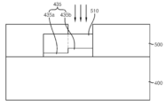
도 4는 본 발명의 실시 예에 따른 싱글 폴리형 이이피롬에서 플로팅 게이트의 구조를 설명하기 위한 단면도이다.4 is a cross-sectional view illustrating a structure of a floating gate in a single poly type ypyrom according to an embodiment of the present invention.
도 4에 도시된 바와 같이, 반도체 기판(미도시됨) 상에 제 2 도전형 웰(400), 예컨데 N 웰이 형성되어 있고, 제 2 도전형 웰(400) 내부에 소스 및 드레인 영역(410, 420)이 형성되어 있다. 또한, 터널 산화막(430, 435) 및 터널 산화막(130)의 상부에 셀렉트 게이트(440) 및 플로팅 게이트(450)이 형성되어 있다. As shown in FIG. 4, a second
한편, 셀렉트 게이트(440) 및 플로팅 게이트(450) 사이의 제 2 도전형 웰(100) 내부에는 고농도 불순물 영역(460)이 형성되어 있다.Meanwhile, a high
본 발명의 실시 예에서 소스 및 드레인 영역(410, 420)과 고농도 불순물 영역(460)은 제 1 도전형 불순물 이온, 예컨대 P 타입의 불순물 이온을 이용하여 형성될 수 있다.In an embodiment of the present invention, the source and drain
본 발명의 실시 예에서 플로팅 게이트(450) 내부에는 서로 다른 농도 분포를 갖는 제 2 도전형 불순물 이온이 도핑되어 있다. 즉, 플로팅 게이트(450)는 드레인 영역(420)에 인접한 제 1 영역(450a)의 농도가 고농도 불순물 영역(460)과 인접한 제 2 영역(450b) 보다 높을 수 있다.In the exemplary embodiment of the present invention, the second conductive type impurity ions having different concentration distributions are doped in the floating
또한, 이러한 플로팅 게이트(450)는 제 1 영역(450a)의 폭이 제 2 영역(450b) 보다 크게 형성될 수 있다. In addition, the floating
한편, 플로팅 게이트(450)는, 도 5에 도시된 바와 같이, 제 1 영역(450a)의 일부가 식각된 패턴을 갖도록 형성될 수 있는데, 예컨대 다수의 요철 모양의 식각 패턴을 갖도록 형성될 수 있다. 즉, 기 설정된 간격(d), 예컨대 0.5㎛~0.7㎛ 간격으로 요철 모양을 갖는 패턴을 제 1 영역(450a)에 형성함으로써, 제 1 영역(450a)에서 전계 밀집 현상을 유발시킬 수 있다.Meanwhile, as shown in FIG. 5, the floating
상술한 바와 같이, 제 1 영역(450a)의 일부가 요철 모양의 식각 패턴을 갖음으로써, 플로팅 게이트(450)의 하부 제 2 도전형 웰(400) 내부에 형성된 채널 영역(470)을 통해 전하가 이동할 때 제 1 영역(450a)에서 전계 밀집(electronic field crowding) 현상을 유발시킬 수 있기 때문에 동작 전압을 낮출 수 있다.As described above, since a part of the
본 발명의 실시 예에 따른 플로팅 게이트(450)의 하부에 형성된 터널 산화막(435)은 저전압용 터널 산화막(435a) 및 고전압용 터널 산화막(435b)으로 형성될 수 있다. 즉, 플로팅 게이트(450)의 제 2 영역(130) 하부에는 셀렉트 게이트(440)과 드레인 영역(420)에 저전압, 예컨대 -7V의 전압이 인가될 때 전하가 트랩되는 저전압용 터널 산화막(435a)가 형성되어 있다. The
한편, 셀렉트 게이트(440)과 드레인 영역(420)에 고전압, 예컨대 -20V의 전압이 인가될 때에는 채널 영역(470)을 통해 이동하는 전하가 저전압용 터널 산화막(430a)뿐만 아니라 고전압용 터널 산화막(435b)에도 전하가 트랩될 수 있다.On the other hand, when a high voltage, for example, -20V, is applied to the
또한, 저전압용 터널 산화막(435a)은 고전압용 터널 산화막(435b)보다 두께가 더 얇게 형성될 수 있다. Further, the low voltage
상술한 바와 같은 구조를 갖는 싱글 폴리형 이이피롬은 전자 주입 방식으로 프로그래밍되어 동작할 수 있다. 이에 대해 설명하면 아래와 같다.The single polytype ypyrom having the structure as described above may be programmed and operated by electron injection. This is described below.
도 6a에 도시된 바와 같이, 저전압의 프로그램 동작에서, 셀렉트 게이트(440)에 셀렉트 전압(Vsg) -7V를 인가하고, 드레인 영역(420)에 드레인 전압(Vdd) -7V를 인가한다. 이 경우, 트랜지스터는 턴 온되어 채널 영역(470)을 통해 전류가 흐른다. 이때, 발생된 열 전자(hot electron)중 일부는 게이트의 수직 방향으로 형성된 전계(electric field)에 의해 플로팅 게이트(450)의 하부에 형성된 터널 산화막(435) 중 저전압용 터널 산화막(435a)에만 전하가 트랩되게 된다. 이러한 저전압용 터널 산화막(435a)을 통해 플로팅 게이트(450)로 주입된다. 열 전자의 주입에 의해 셀 트랜지스터의 문턱 전압은 초기 전압으로부터 상승된다.As shown in FIG. 6A, in the low voltage program operation, the select voltage Vsg -7V is applied to the
한편, 저전압으로 프로그래밍된 싱글 폴리형 이이피롬을 동작(read-on)시키기 위해서는 셀렉트 게이트(440)에 셀렉트 전압(Vsg) -2.8V를 인가하고, 드레인 영역(420)에 드레인 전압(Vdd) -2.8V를 인가한다.On the other hand, in order to read-on a single poly type ypyrom programmed to a low voltage, a select voltage (Vsg) -2.8V is applied to the
또한, 도 6b에 도시된 바와 같이, 고전압의 프로그램 동작에서 셀렉트 게이트(440)에 셀렉트 전압(Vsg) -20V를 인가하고, 드레인 영역(420)에 드레인 전압(Vdd) -20V를 인가한다. 이 경우, 트랜지스터는 턴 온되어 채널 영역(470)을 통해 전류가 흐른다. 이때, 발생된 열 전자(hot electron)중 일부는 게이트의 수직 방향으로 형성된 전계(electric field)에 의해 플로팅 게이트(450)의 터널 산화막(435) 전체에 전하가 트랩되게 된다. 이러한 열전자는 터널 산화막(435)을 통해 플로팅 게이트(450)로 주입된다. 열 전자의 주입에 의해 셀 트랜지스터의 문턱 전압은 초기 전압으로부터 상승된다.In addition, as illustrated in FIG. 6B, the select voltage Vsg −20 V is applied to the
한편, 고전압으로 프로그래밍된 싱글 폴리형 이이피롬을 동작(read-on)시키기 위해서는 셀렉트 게이트(440)에 셀렉트 전압(Vsg) -2.8V를 인가하고, 드레인 영역(420)에 드레인 전압(Vdd) -1.3를 인가한다.On the other hand, in order to read-on a single poly type ypyrom programmed to a high voltage, a select voltage (Vsg) -2.8V is applied to the
상술한 바와 같이, 서로 다른 두께를 갖는 터널 산화막(435)을 플로팅 게이트(450)의 하부에 형성함으로써, 하나의 셀을 이용하여 두 가지 형태의 프로그래밍이 가능하기 때문에 셀 밀도를 증가시킬 수 있을 뿐만 아니라 셀의 단위 면적을 줄일 수 있다.As described above, by forming the
상기와 같은 구조를 갖는 싱글 폴리형 이이피롬에서 플로팅 게이트를 형성하는 과정에 대해 도 7a 내지 도 7을 참조하여 설명한다.A process of forming the floating gate in the single poly type ypyrom having the above structure will be described with reference to FIGS. 7A to 7.
도 7a에 도시된 바와 같이, 반도체 기판(미도시됨)에 제 2 도전형 웰(400)을 형성한 후 제 2 도전형 웰(400)의 상부에 저전압용 및 고전압용 터널 산화막(435a, 435b)을 형성한다. 즉, 제 2 도전형 웰(400)이 형성된 반도체 기판 상에 산화막을 증착한 후 서로 다른 식각 비율로 산화막을 식각함으로써, 저전압용 및 고전압용 터널 산화막(435a, 435b)을 형성한다. 여기에서, 고전압용 터널 산화막(435b)은 저전압용 터널 산화막(435a)의 두께보다 더 두껍게 형성된다.As shown in FIG. 7A, after forming the second conductivity type well 400 in a semiconductor substrate (not shown), the
그런 다음, 도 7b에 도시된 바와 같이, 저전압용 및 고전압용 터널 산화막(435a, 435b)이 형성된 결과물 상에 폴리실리콘을 증착한 후 폴리실리콘을 식각하여 저전압용 및 고전압용 터널 산화막(435a, 435b)의 상부에 플로팅 게이트(450)를 형성한다.Then, as shown in FIG. 7B, polysilicon is deposited on the resultant product on which the low voltage and high voltage
이후, 도 7c에 도시된 바와 같이, 플로팅 게이트(450)의 제 1 영역(450a)의 상부만 오픈된 포토레지스트 패턴(500)을 형성한 후 포토레지스트 패턴(500)을 이온 주입 마스크로 한 제 2 도전형 불순물 이온 주입 공정을 실시하여 제 1 영역(450a)에 제 2 도전형 불순물 이온 영역(510)을 형성한다.Subsequently, as shown in FIG. 7C, after forming the
그리고 나서, 도 7d에 도시된 바와 같이, 포토레지스트 패턴(500)을 스트립 공정을 통해 제거하고, 열확산 공정을 실시하여 플로팅 게이트(450)의 제 1 영역(450a)에 고농도 제 2 도전형 불순물 영역(510a)을 형성함과 더불어 제 1 영역(450a) 내 제 2 도전형 불순물 이온의 확산을 통해 제 2 영역(450b)에 저농도 제 2 도전형 불순물 영역(510b)을 형성함으로써, 고농도 및 저농도 제 2 도전형 불순물 영역(510a, 510b)으로 이루어진 플로팅 게이트(450)를 형성한다.Then, as illustrated in FIG. 7D, the
이후, 도 7e에 도시된 바와 같이, 고농도 제 1 도전형 불순물 이온 주입 공정을 실시하여 플로팅 게이트(450)에 의해 드러난 제 2 도전형 웰(400) 내부에 고농도 불순물 영역(460) 및 드레인 영역(420)을 형성한다.Thereafter, as illustrated in FIG. 7E, a high concentration first impurity ion implantation process is performed to form a high
한편, 본 발명의 실시 예에서는 생략되었지만, 플로팅 게이트(450)을 형성한 후 제 1 영역(450a)의 플로팅 게이트(450) 일부분을 식각하여 식각된 패턴을 형성하거나, 고농도 및 저농도 제 2 도전형 불순물 영역(510a, 510b)을 형성한 후 제 1 영역(450a)의 플로팅 게이트(450) 일부분을 식각하여 식각된 패턴을 형성할 수 있다.Meanwhile, although omitted in the embodiment of the present invention, after forming the floating
본 발명의 실시 예에 따르면, 플로팅 게이트(450)의 하부에 형성되는 터널 산화막(435)을 서로 다른 두께로 형성함으로써, 하나의 플로팅 게이트(450)를 이용하여 두 가지 형태의 프로그래밍이 가능할 수 있다.According to an embodiment of the present disclosure, by forming the
또한, 서로 다른 제 2 도전형 불순물 농도 분포를 갖는 플로팅 게이트(450)를 제공함으로써, 플로팅 게이트(450)의 일함수(workfunction) 차이를 이용하여 동작 전압 차이를 유발할 수 있다.In addition, by providing a floating
이상 첨부된 도면을 참조하여 본 발명의 실시예를 설명하였지만, 본 발명이 속하는 기술분야에서 통상의 지식을 가진 자는 본 발명이 그 기술적 사상이나 필수적인 특징을 변경하지 않고서 다른 구체적인 형태로 실시될 수 있다는 것을 이해할 수 있을 것이다.
While the present invention has been described in connection with what is presently considered to be practical exemplary embodiments, it is to be understood that the invention is not limited to the disclosed embodiments, but, on the contrary, You will understand.
400 : 제 1 도전형 웰
410, 420 : 소스 및 드레인 영역
430, 435 : 터널 산화막
435a : 저전압 터널 산화막
435b : 고전압 터널 산화막
450 : 플로팅 게이트
450a : 제 1 영역
450b : 제 2 영역
460 : 고농도 불순물 영역
470 : 채널 영역400: first conductivity type well
410 and 420: source and drain regions
430, 435 tunnel oxide film
435a: low voltage tunnel oxide
435b: high voltage tunnel oxide
450: floating gate
450a: first region
450b: second region
460: high concentration impurity region
470: channel area
Claims (13)
상기 제 2 도전형 웰의 내부에 형성된 제 1 도전형의 소스 및 드레인 영역과,
상기 제 2 도전형 웰의 상부에 형성된 터널 산화막과,
상기 터널 산화막 상부에 형성되며, 제 2 도전형 불순물 이온이 도핑되며, 상기 드레인 영역과 인접한 일부에 식각된 패턴을 갖는 플로팅 게이트와,
상기 플로팅 게이트와 인접한 상기 제 2 도전형 웰의 내부에 형성된 제 1 도전형의 불순물 영역을 포함하며,
상기 플로팅 게이트는, 상기 드레인 영역과 인접한 부분의 농도가 상기 불순물 영역과 인접한 부분 보다 높은 것을 특징으로 하는
싱글 폴리형 이이피롬.
A second conductivity type well formed on the semiconductor substrate,
A source and drain region of a first conductivity type formed in the second conductivity type well;
A tunnel oxide film formed over the second conductivity type well,
A floating gate formed on the tunnel oxide layer, doped with second conductivity type impurity ions, and having a pattern etched in a portion adjacent to the drain region;
An impurity region of a first conductivity type formed in the second conductivity type well adjacent to the floating gate;
The floating gate is characterized in that the concentration of the portion adjacent to the drain region is higher than the portion adjacent to the impurity region.
Single polypyropyrom.
상기 플로팅 게이트는, 상기 드레인 영역과 인접한 부분의 폭이 상기 불순물 영역과 인접한 부분 보다 큰 것을 특징으로 하는
싱글 폴리형 이이피롬.
The method of claim 1,
The floating gate is characterized in that the width of the portion adjacent to the drain region is larger than the portion adjacent to the impurity region.
Single polypyropyrom.
상기 플로팅 게이트는, 상기 드레인 영역과 인접한 일부가 요철 모양으로 패터닝되어 있는 것을 특징으로 하는
싱글 폴리형 이이피롬.
The method of claim 1,
The floating gate has a portion adjacent to the drain region patterned in a concave-convex shape.
Single polypyropyrom.
상기 싱글 폴리형 이이피롬은, 핫 전자 주입 방식으로 프로그래밍을 수행하는 것을 특징으로 하는
싱글 폴리형 이이피롬.
The method of claim 1,
The single poly type Y pyrom, characterized in that for performing the programming by hot electron injection method
Single polypyropyrom.
상기 터널 산화막은,
상기 드레인 영역과 인접한 부분의 두께가 상기 불순물 영역과 인접한 부분의 두께보다 더 두꺼운 것을 특징으로 하는
싱글 폴리형 이이피롬.
The method of claim 1,
The tunnel oxide film,
The thickness of the portion adjacent to the drain region is thicker than the thickness of the portion adjacent to the impurity region.
Single polypyropyrom.
상기 제 1 도전형은 p형 불순물이며, 상기 제 2 도전형은 n형 불순물인 것을 특징으로 하는
싱글 폴리형 이이피롬.
The method of claim 1,
Wherein the first conductivity type is a p-type impurity and the second conductivity type is an n-type impurity
Single polypyropyrom.
상기 제 2 도전형의 웰이 형성된 반도체 기판 상부에 터널 산화막을 형성하는 단계와,
상기 터널 산화막의 상부에 플로팅 게이트를 형성하는 단계와,
상기 플로팅 게이트의 일부분에 대한 제 2 도전형 불순물 이온 주입 공정을 실시하여 상기 플로팅 게이트의 일부분에 제 2 도전형 불순물 영역을 형성하는 단계와,
상기 제 2 도전형 불순물 영역에 대한 열확산 공정을 실시하여 상기 플로팅 게이트의 일부분에 고농도 제 2 도전형 불순물 영역과 상기 플로팅 게이트의 다른 부분에 저농도 제 2 도전형 불순물 영역을 형성하는 단계와,
상기 고농도 제 2 도전형 불순물 영역 중 드레인 영역과 인접한 일부를 패터닝하는 단계와,
상기 플로팅 게이트의 양측에 의해 드러난 상기 제 2 도전형 웰 내부에 제 1 도전형 불순물 이온 주입 공정을 실시하여 소스 및 드레인 영역과 불순물 영역을 형성하는 단계를 포함하는
싱글 폴리형 이이피롬 제조 방법.
Forming a well of a second conductivity type in the semiconductor substrate,
Forming a tunnel oxide film on the semiconductor substrate on which the wells of the second conductivity type are formed;
Forming a floating gate on the tunnel oxide layer;
Performing a second conductivity type impurity ion implantation process on a portion of the floating gate to form a second conductivity type impurity region in the portion of the floating gate;
Performing a thermal diffusion process on the second conductivity type impurity region to form a high concentration second conductivity type impurity region in a portion of the floating gate and a low concentration second conductivity type impurity region in another portion of the floating gate;
Patterning a portion of the high concentration second conductivity type impurity region adjacent to the drain region;
Forming a source and drain region and an impurity region by performing a first conductivity type impurity ion implantation process in the second conductivity type well exposed by both sides of the floating gate;
Method for producing a single polypyropyrom.
상기 패터닝하는 단계는,
상기 드레인 영역과 인접한 일부를 요철 모양으로 패터닝하는 것을 특징으로 하는
싱글 폴리형 이이피롬 제조 방법.
The method of claim 8,
The patterning step,
A portion adjacent to the drain region is patterned in a concave-convex shape.
Method for producing a single polypyropyrom.
상기 저농도 제 2 도전형 불순물 영역을 형성하는 단계는,
상기 드레인 영역과 인접한 상기 플로팅 게이트의 일부분만 오프된 마스크 패턴을 형성하는 단계와,
상기 마스크 패턴을 이온 주입 마스크로 한 상기 제 2 도전형 불순물 이온 주입 공정을 실시하여 상기 플로팅 게이트의 일부분에 제 2 도전형 불순물 이온을 주입하는 단계와,
상기 마스크 패턴을 제거한 후 상기 제 2 도전형 불순물 이온 주입된 플로팅 게이트에 대한 열 확산 공정을 실시하여 상기 플로팅 게이트 내부에 상기 고농도 제 2 도전형 불순물 영역과 저농도 제 2 도전형 불순물 영역을 형성하는 단계를 포함하는
싱글 폴리형 이이피롬 제조 방법.
The method of claim 8,
Forming the low concentration second conductivity type impurity region,
Forming a mask pattern in which only a part of the floating gate adjacent to the drain region is turned off;
Implanting a second conductivity type impurity ion into the portion of the floating gate by performing the second conductivity type impurity ion implantation process using the mask pattern as an ion implantation mask;
Removing the mask pattern and performing a thermal diffusion process on the floating gate implanted with the second conductivity type impurity ions to form the high concentration second conductivity type impurity region and the low concentration second conductivity type impurity region in the floating gate; Containing
Method for producing a single polypyropyrom.
상기 터널 산화막을 형성하는 단계는,
상기 고농도 제 2 도전형 불순물 영역에 대응되는 부분이 상기 저농도 제 2 도전형 불순물 영역에 대응되는 부분보다 두께가 더 두꺼운 상기 터널 산화막을 형성하는 것을 특징으로 하는
싱글 폴리형 이이피롬 제조 방법.
The method of claim 8,
Forming the tunnel oxide film,
Wherein the portion corresponding to the high concentration second conductivity type impurity region forms the tunnel oxide film that is thicker than the portion corresponding to the low concentration second conductivity type impurity region.
Method for producing a single polypyropyrom.
상기 제 1 도전형은 p형 불순물이며, 상기 제 2 도전형은 n형 불순물인 것을 특징으로 하는
싱글 폴리형 이이피롬 제조 방법. The method of claim 8,
Wherein the first conductivity type is a p-type impurity and the second conductivity type is an n-type impurity
Method for producing a single polypyropyrom.
Priority Applications (2)
| Application Number | Priority Date | Filing Date | Title |
|---|---|---|---|
| KR1020110146422A KR101334844B1 (en) | 2011-12-29 | 2011-12-29 | Single poly eeprom and method for fabricating the same |
| US13/463,268 US8648406B2 (en) | 2011-12-29 | 2012-05-03 | Single poly EEPROM having a tunnel oxide layer |
Applications Claiming Priority (1)
| Application Number | Priority Date | Filing Date | Title |
|---|---|---|---|
| KR1020110146422A KR101334844B1 (en) | 2011-12-29 | 2011-12-29 | Single poly eeprom and method for fabricating the same |
Publications (2)
| Publication Number | Publication Date |
|---|---|
| KR20130077616A KR20130077616A (en) | 2013-07-09 |
| KR101334844B1 true KR101334844B1 (en) | 2013-12-05 |
Family
ID=48694149
Family Applications (1)
| Application Number | Title | Priority Date | Filing Date |
|---|---|---|---|
| KR1020110146422A Expired - Fee Related KR101334844B1 (en) | 2011-12-29 | 2011-12-29 | Single poly eeprom and method for fabricating the same |
Country Status (2)
| Country | Link |
|---|---|
| US (1) | US8648406B2 (en) |
| KR (1) | KR101334844B1 (en) |
Families Citing this family (7)
| Publication number | Priority date | Publication date | Assignee | Title |
|---|---|---|---|---|
| US9312014B2 (en) * | 2013-04-01 | 2016-04-12 | SK Hynix Inc. | Single-layer gate EEPROM cell, cell array including the same, and method of operating the cell array |
| US9978848B2 (en) * | 2015-07-17 | 2018-05-22 | Avago Technologies General Ip (Singapore) Pte. Ltd. | UTBB FDSOI split gate devices |
| US9899485B2 (en) | 2016-06-07 | 2018-02-20 | International Business Machines Corporation | Spatially decoupled floating gate semiconductor device |
| CN114551452A (en) | 2016-10-21 | 2022-05-27 | 联华电子股份有限公司 | Single-layer polysilicon electronically erasable rewritable read-only memory |
| KR102460296B1 (en) * | 2018-01-30 | 2022-10-31 | 주식회사 키파운드리 | Single Poly Multi Time Program Cell and its operation method |
| US11641739B2 (en) * | 2020-06-01 | 2023-05-02 | Globalfoundries Singapore Pte. Ltd. | Semiconductor non-volatile memory devices |
| JP2023089475A (en) * | 2021-12-16 | 2023-06-28 | タワー パートナーズ セミコンダクター株式会社 | semiconductor equipment |
Citations (4)
| Publication number | Priority date | Publication date | Assignee | Title |
|---|---|---|---|---|
| KR100745030B1 (en) * | 2006-01-27 | 2007-08-01 | 충북대학교 산학협력단 | Flash memory device, manufacturing method thereof and driving method thereof |
| KR20090050389A (en) * | 2007-11-15 | 2009-05-20 | 삼성전자주식회사 | Gate Structure, Non-Volatile Memory Cell and Manufacturing Method Thereof |
| KR20100079176A (en) * | 2008-12-30 | 2010-07-08 | 주식회사 동부하이텍 | Eeprom device and its fabrication method |
| US8383475B2 (en) * | 2010-09-23 | 2013-02-26 | Globalfoundries Singapore Pte. Ltd. | EEPROM cell |
Family Cites Families (17)
| Publication number | Priority date | Publication date | Assignee | Title |
|---|---|---|---|---|
| US4958321A (en) * | 1988-09-22 | 1990-09-18 | Advanced Micro Devices, Inc. | One transistor flash EPROM cell |
| US5063423A (en) * | 1989-04-28 | 1991-11-05 | Nippondenso Co., Ltd. | Semiconductor memory device of a floating gate tunnel oxide type |
| US5780893A (en) * | 1995-12-28 | 1998-07-14 | Nippon Steel Corporation | Non-volatile semiconductor memory device including memory transistor with a composite gate structure |
| DE19614011C2 (en) * | 1996-04-09 | 2002-06-13 | Infineon Technologies Ag | Semiconductor component in which the tunnel gate electrode and the channel gate electrode are interrupted by an insulation structure at the interface with the tunnel dielectric or gate dielectric |
| IT1289524B1 (en) * | 1996-12-24 | 1998-10-15 | Sgs Thomson Microelectronics | MEMORY CELL FOR EEPROM TYPE DEVICES AND RELATED MANUFACTURING PROCESS |
| US6121666A (en) * | 1997-06-27 | 2000-09-19 | Sun Microsystems, Inc. | Split gate oxide asymmetric MOS devices |
| JP3446592B2 (en) * | 1998-03-23 | 2003-09-16 | トヨタ自動車株式会社 | Nonvolatile memory device and method of manufacturing the same |
| EP0969507B1 (en) * | 1998-06-30 | 2006-11-15 | STMicroelectronics S.r.l. | EEPROM memory cell manufacturing method |
| US6313498B1 (en) * | 1999-05-27 | 2001-11-06 | Actrans System Inc. | Flash memory cell with thin floating gate with rounded side wall, and fabrication process |
| KR100298586B1 (en) * | 1999-07-13 | 2001-11-01 | 윤종용 | Non-Volatile Memory device |
| TW437100B (en) * | 1999-08-19 | 2001-05-28 | Taiwan Semiconductor Mfg | Erasable programmable logic device structure and the forming method thereof |
| US6479351B1 (en) * | 2000-11-30 | 2002-11-12 | Atmel Corporation | Method of fabricating a self-aligned non-volatile memory cell |
| JP4809545B2 (en) * | 2001-05-31 | 2011-11-09 | 株式会社半導体エネルギー研究所 | Semiconductor non-volatile memory and electronic device |
| US6465307B1 (en) * | 2001-11-30 | 2002-10-15 | Texas Instruments Incorporated | Method for manufacturing an asymmetric I/O transistor |
| US7164177B2 (en) * | 2004-01-02 | 2007-01-16 | Powerchip Semiconductor Corp. | Multi-level memory cell |
| US8026545B2 (en) * | 2008-12-01 | 2011-09-27 | Rohm Co., Ltd. | Eeprom |
| KR101277147B1 (en) * | 2009-12-10 | 2013-06-20 | 한국전자통신연구원 | Electrically Erasable Programmable Read-Only Memory(EEPROM) apparatus and method of fabricating the same |
-
2011
- 2011-12-29 KR KR1020110146422A patent/KR101334844B1/en not_active Expired - Fee Related
-
2012
- 2012-05-03 US US13/463,268 patent/US8648406B2/en active Active
Patent Citations (4)
| Publication number | Priority date | Publication date | Assignee | Title |
|---|---|---|---|---|
| KR100745030B1 (en) * | 2006-01-27 | 2007-08-01 | 충북대학교 산학협력단 | Flash memory device, manufacturing method thereof and driving method thereof |
| KR20090050389A (en) * | 2007-11-15 | 2009-05-20 | 삼성전자주식회사 | Gate Structure, Non-Volatile Memory Cell and Manufacturing Method Thereof |
| KR20100079176A (en) * | 2008-12-30 | 2010-07-08 | 주식회사 동부하이텍 | Eeprom device and its fabrication method |
| US8383475B2 (en) * | 2010-09-23 | 2013-02-26 | Globalfoundries Singapore Pte. Ltd. | EEPROM cell |
Also Published As
| Publication number | Publication date |
|---|---|
| US8648406B2 (en) | 2014-02-11 |
| KR20130077616A (en) | 2013-07-09 |
| US20130168755A1 (en) | 2013-07-04 |
Similar Documents
| Publication | Publication Date | Title |
|---|---|---|
| KR100468745B1 (en) | Non-volatile memory cell having a silicon-oxide-nitride-oxide-silicon gate structure and fabrication method of such cell | |
| US8860459B2 (en) | Semiconductor integrated circuit, programmable logic device, method of manufacturing semiconductor integrated citcuit | |
| JP3733595B2 (en) | Manufacturing method of semiconductor device including MOS element | |
| CN103904082B (en) | Nonvolatile memory structure and method for fabricating nonvolatile memory structure | |
| KR101334844B1 (en) | Single poly eeprom and method for fabricating the same | |
| JPWO1998034275A1 (en) | Semiconductor device including MOS element and manufacturing method thereof | |
| JP2939537B2 (en) | Flash memory and manufacturing method thereof | |
| US7136306B2 (en) | Single bit nonvolatile memory cell and methods for programming and erasing thereof | |
| US6774428B1 (en) | Flash memory structure and operating method thereof | |
| US20020121657A1 (en) | Double-bit non-volatile memory structure and corresponding method of manufacture | |
| KR100273705B1 (en) | Method for fabricating of nonvolatile memory device and well structure thereof | |
| US8072803B2 (en) | Memory device and methods for fabricating and operating the same | |
| US7439133B2 (en) | Memory structure and method of manufacturing a memory array | |
| KR20150120816A (en) | Non-volatile memory cell having single-layer gate, method of operating the same, and memory cell array using the same | |
| US7008846B2 (en) | Non-volatile floating gate memory cell with floating gates formed as spacers, and an array thereof, and a method of manufacturing | |
| KR100752192B1 (en) | Flash memory device with single poly structure and manufacturing method thereof | |
| KR100757326B1 (en) | Nonvolatile Memory Device, Manufacturing Method and Operation Method thereof | |
| KR100685880B1 (en) | Flash Y pyrom cell and manufacturing method thereof | |
| KR101111917B1 (en) | Non-volatile memory cell using state of three kinds and method of manufacturing the same | |
| JP2793722B2 (en) | Nonvolatile semiconductor memory device and method of manufacturing the same | |
| JP3948535B2 (en) | Nonvolatile semiconductor memory device and manufacturing method thereof | |
| KR100688489B1 (en) | Nonvolatile Memory and Manufacturing Method Thereof | |
| KR100186507B1 (en) | Structure of flash memory device and its manufacturing method | |
| KR20090070269A (en) | Flash memory device and manufacturing method thereof | |
| KR20080079010A (en) | Multi-bit flash memory cell, driving method thereof and manufacturing method thereof |
Legal Events
| Date | Code | Title | Description |
|---|---|---|---|
| A201 | Request for examination | ||
| PA0109 | Patent application |
St.27 status event code: A-0-1-A10-A12-nap-PA0109 |
|
| PA0201 | Request for examination |
St.27 status event code: A-1-2-D10-D11-exm-PA0201 |
|
| D13-X000 | Search requested |
St.27 status event code: A-1-2-D10-D13-srh-X000 |
|
| D14-X000 | Search report completed |
St.27 status event code: A-1-2-D10-D14-srh-X000 |
|
| E902 | Notification of reason for refusal | ||
| PE0902 | Notice of grounds for rejection |
St.27 status event code: A-1-2-D10-D21-exm-PE0902 |
|
| PG1501 | Laying open of application |
St.27 status event code: A-1-1-Q10-Q12-nap-PG1501 |
|
| E13-X000 | Pre-grant limitation requested |
St.27 status event code: A-2-3-E10-E13-lim-X000 |
|
| P11-X000 | Amendment of application requested |
St.27 status event code: A-2-2-P10-P11-nap-X000 |
|
| P13-X000 | Application amended |
St.27 status event code: A-2-2-P10-P13-nap-X000 |
|
| E701 | Decision to grant or registration of patent right | ||
| PE0701 | Decision of registration |
St.27 status event code: A-1-2-D10-D22-exm-PE0701 |
|
| GRNT | Written decision to grant | ||
| PR0701 | Registration of establishment |
St.27 status event code: A-2-4-F10-F11-exm-PR0701 |
|
| PR1002 | Payment of registration fee |
St.27 status event code: A-2-2-U10-U11-oth-PR1002 Fee payment year number: 1 |
|
| PG1601 | Publication of registration |
St.27 status event code: A-4-4-Q10-Q13-nap-PG1601 |
|
| L13-X000 | Limitation or reissue of ip right requested |
St.27 status event code: A-2-3-L10-L13-lim-X000 |
|
| U15-X000 | Partial renewal or maintenance fee paid modifying the ip right scope |
St.27 status event code: A-4-4-U10-U15-oth-X000 |
|
| FPAY | Annual fee payment |
Payment date: 20161013 Year of fee payment: 4 |
|
| PR1001 | Payment of annual fee |
St.27 status event code: A-4-4-U10-U11-oth-PR1001 Fee payment year number: 4 |
|
| PR1001 | Payment of annual fee |
St.27 status event code: A-4-4-U10-U11-oth-PR1001 Fee payment year number: 5 |
|
| PN2301 | Change of applicant |
St.27 status event code: A-5-5-R10-R13-asn-PN2301 St.27 status event code: A-5-5-R10-R11-asn-PN2301 |
|
| PR1001 | Payment of annual fee |
St.27 status event code: A-4-4-U10-U11-oth-PR1001 Fee payment year number: 6 |
|
| PC1903 | Unpaid annual fee |
St.27 status event code: A-4-4-U10-U13-oth-PC1903 Not in force date: 20191126 Payment event data comment text: Termination Category : DEFAULT_OF_REGISTRATION_FEE |
|
| R18-X000 | Changes to party contact information recorded |
St.27 status event code: A-5-5-R10-R18-oth-X000 |
|
| PC1903 | Unpaid annual fee |
St.27 status event code: N-4-6-H10-H13-oth-PC1903 Ip right cessation event data comment text: Termination Category : DEFAULT_OF_REGISTRATION_FEE Not in force date: 20191126 |
|
| P22-X000 | Classification modified |
St.27 status event code: A-4-4-P10-P22-nap-X000 |
|
| P22-X000 | Classification modified |
St.27 status event code: A-4-4-P10-P22-nap-X000 |
|
| P22-X000 | Classification modified |
St.27 status event code: A-4-4-P10-P22-nap-X000 |