KR101261609B1 - Thin film transistor, thin film transistor array panel and method for manufacturing the same - Google Patents
Thin film transistor, thin film transistor array panel and method for manufacturing the same Download PDFInfo
- Publication number
- KR101261609B1 KR101261609B1 KR1020060063588A KR20060063588A KR101261609B1 KR 101261609 B1 KR101261609 B1 KR 101261609B1 KR 1020060063588 A KR1020060063588 A KR 1020060063588A KR 20060063588 A KR20060063588 A KR 20060063588A KR 101261609 B1 KR101261609 B1 KR 101261609B1
- Authority
- KR
- South Korea
- Prior art keywords
- film
- polycrystalline
- electrode
- semiconductor
- gate
- Prior art date
- Legal status (The legal status is an assumption and is not a legal conclusion. Google has not performed a legal analysis and makes no representation as to the accuracy of the status listed.)
- Expired - Fee Related
Links
Images


Classifications
-
- H—ELECTRICITY
- H10—SEMICONDUCTOR DEVICES; ELECTRIC SOLID-STATE DEVICES NOT OTHERWISE PROVIDED FOR
- H10D—INORGANIC ELECTRIC SEMICONDUCTOR DEVICES
- H10D30/00—Field-effect transistors [FET]
- H10D30/01—Manufacture or treatment
- H10D30/021—Manufacture or treatment of FETs having insulated gates [IGFET]
- H10D30/031—Manufacture or treatment of FETs having insulated gates [IGFET] of thin-film transistors [TFT]
- H10D30/0312—Manufacture or treatment of FETs having insulated gates [IGFET] of thin-film transistors [TFT] characterised by the gate electrodes
- H10D30/0316—Manufacture or treatment of FETs having insulated gates [IGFET] of thin-film transistors [TFT] characterised by the gate electrodes of lateral bottom-gate TFTs comprising only a single gate
-
- H—ELECTRICITY
- H10—SEMICONDUCTOR DEVICES; ELECTRIC SOLID-STATE DEVICES NOT OTHERWISE PROVIDED FOR
- H10D—INORGANIC ELECTRIC SEMICONDUCTOR DEVICES
- H10D30/00—Field-effect transistors [FET]
- H10D30/01—Manufacture or treatment
- H10D30/021—Manufacture or treatment of FETs having insulated gates [IGFET]
- H10D30/031—Manufacture or treatment of FETs having insulated gates [IGFET] of thin-film transistors [TFT]
- H10D30/0321—Manufacture or treatment of FETs having insulated gates [IGFET] of thin-film transistors [TFT] comprising silicon, e.g. amorphous silicon or polysilicon
-
- H—ELECTRICITY
- H10—SEMICONDUCTOR DEVICES; ELECTRIC SOLID-STATE DEVICES NOT OTHERWISE PROVIDED FOR
- H10D—INORGANIC ELECTRIC SEMICONDUCTOR DEVICES
- H10D30/00—Field-effect transistors [FET]
- H10D30/60—Insulated-gate field-effect transistors [IGFET]
- H10D30/67—Thin-film transistors [TFT]
- H10D30/6704—Thin-film transistors [TFT] having supplementary regions or layers in the thin films or in the insulated bulk substrates for controlling properties of the device
- H10D30/6708—Thin-film transistors [TFT] having supplementary regions or layers in the thin films or in the insulated bulk substrates for controlling properties of the device for preventing the kink effect or the snapback effect, e.g. discharging the minority carriers of the channel region for preventing bipolar effect
-
- H—ELECTRICITY
- H10—SEMICONDUCTOR DEVICES; ELECTRIC SOLID-STATE DEVICES NOT OTHERWISE PROVIDED FOR
- H10D—INORGANIC ELECTRIC SEMICONDUCTOR DEVICES
- H10D30/00—Field-effect transistors [FET]
- H10D30/60—Insulated-gate field-effect transistors [IGFET]
- H10D30/67—Thin-film transistors [TFT]
- H10D30/6729—Thin-film transistors [TFT] characterised by the electrodes
- H10D30/673—Thin-film transistors [TFT] characterised by the electrodes characterised by the shapes, relative sizes or dispositions of the gate electrodes
- H10D30/6732—Bottom-gate only TFTs
-
- H—ELECTRICITY
- H10—SEMICONDUCTOR DEVICES; ELECTRIC SOLID-STATE DEVICES NOT OTHERWISE PROVIDED FOR
- H10D—INORGANIC ELECTRIC SEMICONDUCTOR DEVICES
- H10D30/00—Field-effect transistors [FET]
- H10D30/60—Insulated-gate field-effect transistors [IGFET]
- H10D30/67—Thin-film transistors [TFT]
- H10D30/674—Thin-film transistors [TFT] characterised by the active materials
- H10D30/6741—Group IV materials, e.g. germanium or silicon carbide
- H10D30/6743—Silicon
- H10D30/6745—Polycrystalline or microcrystalline silicon
-
- H—ELECTRICITY
- H10—SEMICONDUCTOR DEVICES; ELECTRIC SOLID-STATE DEVICES NOT OTHERWISE PROVIDED FOR
- H10D—INORGANIC ELECTRIC SEMICONDUCTOR DEVICES
- H10D30/00—Field-effect transistors [FET]
- H10D30/60—Insulated-gate field-effect transistors [IGFET]
- H10D30/67—Thin-film transistors [TFT]
- H10D30/6757—Thin-film transistors [TFT] characterised by the structure of the channel, e.g. transverse or longitudinal shape or doping profile
-
- H—ELECTRICITY
- H10—SEMICONDUCTOR DEVICES; ELECTRIC SOLID-STATE DEVICES NOT OTHERWISE PROVIDED FOR
- H10D—INORGANIC ELECTRIC SEMICONDUCTOR DEVICES
- H10D86/00—Integrated devices formed in or on insulating or conducting substrates, e.g. formed in silicon-on-insulator [SOI] substrates or on stainless steel or glass substrates
- H10D86/01—Manufacture or treatment
- H10D86/021—Manufacture or treatment of multiple TFTs
- H10D86/0231—Manufacture or treatment of multiple TFTs using masks, e.g. half-tone masks
-
- H—ELECTRICITY
- H10—SEMICONDUCTOR DEVICES; ELECTRIC SOLID-STATE DEVICES NOT OTHERWISE PROVIDED FOR
- H10D—INORGANIC ELECTRIC SEMICONDUCTOR DEVICES
- H10D86/00—Integrated devices formed in or on insulating or conducting substrates, e.g. formed in silicon-on-insulator [SOI] substrates or on stainless steel or glass substrates
- H10D86/40—Integrated devices formed in or on insulating or conducting substrates, e.g. formed in silicon-on-insulator [SOI] substrates or on stainless steel or glass substrates characterised by multiple TFTs
- H10D86/60—Integrated devices formed in or on insulating or conducting substrates, e.g. formed in silicon-on-insulator [SOI] substrates or on stainless steel or glass substrates characterised by multiple TFTs wherein the TFTs are in active matrices
-
- H—ELECTRICITY
- H10—SEMICONDUCTOR DEVICES; ELECTRIC SOLID-STATE DEVICES NOT OTHERWISE PROVIDED FOR
- H10K—ORGANIC ELECTRIC SOLID-STATE DEVICES
- H10K59/00—Integrated devices, or assemblies of multiple devices, comprising at least one organic light-emitting element covered by group H10K50/00
- H10K59/10—OLED displays
- H10K59/12—Active-matrix OLED [AMOLED] displays
- H10K59/121—Active-matrix OLED [AMOLED] displays characterised by the geometry or disposition of pixel elements
- H10K59/1213—Active-matrix OLED [AMOLED] displays characterised by the geometry or disposition of pixel elements the pixel elements being TFTs
-
- H—ELECTRICITY
- H10—SEMICONDUCTOR DEVICES; ELECTRIC SOLID-STATE DEVICES NOT OTHERWISE PROVIDED FOR
- H10K—ORGANIC ELECTRIC SOLID-STATE DEVICES
- H10K71/00—Manufacture or treatment specially adapted for the organic devices covered by this subclass
-
- H—ELECTRICITY
- H10—SEMICONDUCTOR DEVICES; ELECTRIC SOLID-STATE DEVICES NOT OTHERWISE PROVIDED FOR
- H10K—ORGANIC ELECTRIC SOLID-STATE DEVICES
- H10K71/00—Manufacture or treatment specially adapted for the organic devices covered by this subclass
- H10K71/20—Changing the shape of the active layer in the devices, e.g. patterning
- H10K71/231—Changing the shape of the active layer in the devices, e.g. patterning by etching of existing layers
- H10K71/233—Changing the shape of the active layer in the devices, e.g. patterning by etching of existing layers by photolithographic etching
Landscapes
- Engineering & Computer Science (AREA)
- Manufacturing & Machinery (AREA)
- Physics & Mathematics (AREA)
- Geometry (AREA)
- Microelectronics & Electronic Packaging (AREA)
- Thin Film Transistor (AREA)
Abstract
본 발명에 따른 박막 트랜지스터는 기판, 기판 위에 형성되어 있는 게이트 전극, 게이트 전극 위에 형성되어 있는 게이트 절연막, 게이트 절연막 위에 형성되어 있으며 게이트 전극과 중첩하는 반도체, 반도체와 일부분이 중첩하는 소스 전극, 그리고 반도체와 일부분이 중첩하는 드레인 전극을 포함하고, 다결정 반도체는 도전성 불순물이 도핑된 복수의 제1 다결정 반도체와 도전형 불순물이 도핑되지 않은 복수의 제2 다결정 반도체를 포함하고 제1 다결정 반도체는 이웃하는 제2 다결정 반도체 사이에 위치하며 제2 다결정 반도체와 직렬로 연결되어 있다.The thin film transistor according to the present invention includes a substrate, a gate electrode formed on the substrate, a gate insulating film formed on the gate electrode, a semiconductor formed on the gate insulating film and overlapping the gate electrode, a source electrode partially overlapping the semiconductor, and a semiconductor. And a drain electrode partially overlapping with each other, wherein the polycrystalline semiconductor includes a plurality of first polycrystalline semiconductors doped with conductive impurities and a plurality of second polycrystalline semiconductors not doped with conductive impurities, and the first polycrystalline semiconductor is adjacent to each other. It is located between two polycrystalline semiconductors and is connected in series with a second polycrystalline semiconductor.
다결정 반도체, 고상 결정화, 바텀 게이트 Polycrystalline Semiconductor, Solid State Crystallization, Bottom Gate
Description
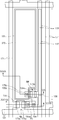
도 1은 본 발명의 한 실시예에 따른 액정 표시 장치의 배치도이다.1 is a layout diagram of a liquid crystal display according to an embodiment of the present invention.
도 2는 도 1의 액정 표시 장치용 박막 트랜지스터 표시판의 배치도이다. FIG. 2 is a layout view of a thin film transistor array panel for the liquid crystal display of FIG. 1.
도 3은 도 1의 액정 표시 장치용 공통 전극 표시판의 배치도이다.FIG. 3 is a layout view of a common electrode display panel for the liquid crystal display of FIG. 1.
도 4 및 도 5는 각각 도 1의 액정 표시 장치를 IV-IV 선 및 V-V 선을 따라 잘라 도시한 단면도이다.4 and 5 are cross-sectional views of the liquid crystal display of FIG. 1 taken along lines IV-IV and V-V, respectively.
도 6은 본 발명의 한 실시예에 다른 박막 트랜지스터 표시판의 제조 공정 중 중간 단계에서의 배치도이다.6 is a layout view at an intermediate stage of a manufacturing process of a thin film transistor array panel according to an exemplary embodiment of the present invention.
도 7 및 도 8은 도 6의 VII-VII선 및 VIII-VIII선을 따라 잘라 도시한 단면도이다.7 and 8 are cross-sectional views taken along the lines VII-VII and VIII-VIII of FIG. 6.
도 9는 도 6의 다음 단계에서의 배치도이다.FIG. 9 is a layout view at the next step of FIG. 6.
도 10 및 도 11은 도 9의 X-X선 및 XI-XI선을 따라 잘라 도시한 단면도이다. 10 and 11 are cross-sectional views taken along the X-X and XI-XI lines of FIG. 9.
도 12는 도 9의 다음 단계에서의 배치도이다.12 is a layout view at the next step of FIG.
도 13 및 도 14는 도 9의 XIII-XIII선 및 XIV-XIV선을 따라 잘라 도시한 단면도이다.13 and 14 are cross-sectional views taken along lines XIII-XIII and XIV-XIV of FIG. 9.
도 15 및 도 16은 도 13 및 도 14의 다음 단계에서의 단면도이고, 도 17은 도 15 및 도 16의 다음 단계에서의 배치도이다.15 and 16 are cross-sectional views at the next steps of FIGS. 13 and 14, and FIG. 17 is a layout view at the next steps of FIGS. 15 and 16.
도 18 및 도 19는 도 17의 XVIII-XVIII선 및 XIX-XIX선을 따라 잘라 도시한 단면도이다. 18 and 19 are cross-sectional views taken along lines XVIII-XVIII and XIX-XIX of FIG. 17.
도 20은 도 17의 다음 단계에서의 배치도이다.FIG. 20 is a layout view at the next step of FIG. 17.
도 21 및 도 22는 도 20의 XXI-XXI선 및 XXII-XXII선을 따라 잘라 도시한 단면도이다. 21 and 22 are cross-sectional views taken along the lines XXI-XXI and XXII-XXII of FIG. 20.
도 23은 도 20의 다음 단계에서의 배치도이다.FIG. 23 is a layout view at the next step of FIG. 20.
도 24 및 도 25는 도 23의 XXIV-XXIV선 및 XXV-XXV선을 따라 잘라 도시한 단면도이다. 24 and 25 are cross-sectional views taken along the lines XXIV-XXIV and XXV-XXV of FIG. 23.
도 26은 본 발명의 한 실시예에 따른 유기 발광 표시 장치의 등가 회로도이다.26 is an equivalent circuit diagram of an organic light emitting diode display according to an exemplary embodiment of the present invention.
도 27은 본 발명의 한 실시예에 따른 유기 발광 표시 장치의 배치도이다.27 is a layout view of an organic light emitting diode display according to an exemplary embodiment.
도 28 및 도 29는 각각 도 27의 유기 발광 표시 장치를 XXVIIX-XXVIII선 및 XXIX-XXIX선을 따라 잘라 도시한 단면도이다.28 and 29 are cross-sectional views of the OLED display of FIG. 27 taken along lines XXVIIX-XXVIII and XXIX-XXIX, respectively.
<도면 부호에 대한 설명><Description of Drawing>
110: 절연 기판 121: 게이트선110: Insulation substrate 121: Gate line
124: 게이트 전극 129: 게이트선의 끝 부분124: gate electrode 129: end of the gate line
131: 유지 전극선 133a, 133b: 유지 전극131: sustain
140: 게이트 절연막 150: 반도체층140: gate insulating film 150: semiconductor layer
151: 선형 반도체 154: 반도체의 돌출부151: linear semiconductor 154: protrusion of semiconductor
161: 선형 저항성 접촉 부재 165: 섬형 저항성 접촉 부재161: linear resistive contact member 165: island resistive contact member
171: 데이터선 173: 소스 전극171: data line 173: source electrode
175: 드레인 전극 179: 데이터선의 끝 부분175: drain electrode 179: end of data line
81, 82: 접촉 보조 부재 180: 보호막81, 82: contact auxiliary member 180: protective film
181, 182, 183a, 183b, 185: 접촉 구멍 181, 182, 183a, 183b, 185: contact hole
191: 화소 전극 220: 차광 부재191: pixel electrode 220: light blocking member
230: 색필터 250: 덮개막230: color filter 250: overcoat
270: 공통 전극 361: 격벽270: common electrode 361: partition wall
370: 유기 발광층370: organic light emitting layer
본 발명은 박막 트랜지스터 표시판 및 그 제조 방법에 관한 것이다.The present invention relates to a thin film transistor array panel and a method of manufacturing the same.
일반적으로 액정 표시 장치(liquid crystal display, LCD), 유기 발광 표시 장치(organic light emitting diode display, OLED display), 전기 영동 표시 장치(electrophoretic display) 등의 평판 표시 장치는 복수 쌍의 전기장 생성 전극과 그 사이에 들어 있는 전기 광학(electro-optical) 활성층을 포함한다. 2. Description of the Related Art In general, a flat panel display device such as a liquid crystal display (LCD), an organic light emitting diode (OLED) display, and an electrophoretic display includes a plurality of pairs of electric field generating electrodes, And an electro-optical active layer interposed therebetween.
한 쌍을 이루는 전기장 생성 전극 중 하나는 통상 스위칭 소자에 연결되어 전기 신호를 인가 받고, 전기 광학 활성층은 이 전기 신호를 광학 신호로 변환함으로써 영상을 표시한다.One of the pair of field generating electrodes is typically connected to a switching element to receive an electrical signal, and the electro-optical active layer converts the electrical signal into an optical signal to display an image.
액정 표시 장치의 경우 전기광학 활성층으로 액정층을 포함하고, 유기 발광 표시 장치의 경우 전기광학 활성층으로 유기 발광층을 포함한다.In the case of the liquid crystal display, the liquid crystal layer is included as the electro-optical active layer, and in the case of the organic light emitting display, the organic light emitting layer is included as the electro-optical active layer.
평판 표시 장치에서는 스위칭 소자로서 삼단자 소자인 박막 트랜지스터(thin film transistor, TFT)를 사용하며, 이 박막 트랜지스터를 제어하기 위한 주사 신호를 전달하는 게이트선(gate line)과 화소 전극에 인가될 신호를 전달하는 데이터선(data line)이 평판 표시 장치에 구비된다.In a flat panel display device, a thin film transistor (TFT), which is a three terminal device, is used as a switching device, and a gate line for transmitting a scan signal for controlling the thin film transistor and a signal to be applied to the pixel electrode A data line to be transmitted is provided in the flat panel display.
박막 트랜지스터는 비정질(amorphous) 반도체 또는 다결정(poly crystalline) 반도체로 이루어진 박막을 포함한다.The thin film transistor includes a thin film made of an amorphous semiconductor or a poly crystalline semiconductor.
비정질 반도체 박막은 낮은 온도에서 형성할 수 있어서 용융점이 낮은 유리 또는 플라스틱을 기판으로 사용하는 표시 장치에 많이 적용된다. 그러나 비정질 반도체 박막은 다결정 반도체 박막에 비하여 누설 전류(leakage current) 측면에서는 유리하나 전계 효과 이동도(field effect mobility)가 낮아서 박막 트랜지스터의 동작 속도를 높이는데 한계가 있다.The amorphous semiconductor thin film may be formed at a low temperature, and thus is widely applied to a display device using glass or plastic having a low melting point as a substrate. However, the amorphous semiconductor thin film is advantageous in terms of leakage current compared to the polycrystalline semiconductor thin film, but has a limitation in increasing the operation speed of the thin film transistor because of low field effect mobility.
이에 반해 다결정 반도체 박막은 높은 전계 효과 이동도를 가진다.In contrast, polycrystalline semiconductor thin films have a high field effect mobility.
그러나 다결정 반도체 박막은 기판 위에서 반도체를 결정화하는 단계가 필요하기 때문에 주로 탑 게이트(top gate) 구조를 채용한다. 이 경우 박막 트랜지스터의 구조 및 공정이 복잡해지고 제조 비용이 현저하게 증가한다.However, the polycrystalline semiconductor thin film mainly adopts a top gate structure because it requires a step of crystallizing the semiconductor on the substrate. In this case, the structure and the process of the thin film transistor are complicated and the manufacturing cost is significantly increased.
최근에는 다결정 실리콘 박막 트랜지스터에도 고상결정화(Solid Phase Crystallization) 방법을 이용하여 바텀 게이트(bottom gate) 구조를 적용하고자 하는 시도가 있다. 그러나, 그러한 구조의 경우 드레인 전극과 반도체가 중첩하는 부분에 강한 수직 전계가 형성됨에 따라 이러한 수직 전계에 의해 가속된 전자가 원자와 충돌하여 원자를 이온화시키며, 이로 인해 발생한 정공이 백채널을 통해 소스 전극 쪽으로 이동하고, 이렇게 이동한 정공이 소스 접합 영역의 전위 장벽(potential barrier)을 낮추게 되어 소스 전극으로부터 더 많은 전하가 주입되는 이른바 킹크 효과(kink effect)가 발생한다. 이러한 킹크 효과는 누설전류를 증가시켜 소비전류를 증가시킴은 물론 크로스토크(Crosstalk)을 유발하는 문제가 있다.Recently, there has been an attempt to apply a bottom gate structure to the polycrystalline silicon thin film transistor using a solid phase crystallization method. However, in such a structure, a strong vertical electric field is formed at the overlapping portion of the drain electrode and the semiconductor, and electrons accelerated by the vertical electric field collide with the atom to ionize the atom, and thus the generated holes are sourced through the back channel. Moving toward the electrode, this moved hole lowers the potential barrier of the source junction region, resulting in a so-called kink effect in which more charge is injected from the source electrode. The kink effect increases the leakage current and increases the current consumption, as well as causing crosstalk.
따라서 본 발명이 이루고자 하는 기술적 과제는 이러한 문제점을 해결하기 위한 것으로서 공정을 단순화하면서도 전계 효과 이동도는 높고 누설 전류는 감소시키는 것이다.Therefore, the technical problem to be achieved by the present invention is to solve such a problem, while simplifying the process, the field effect mobility is high and the leakage current is reduced.
상기한 기술적 과제를 이루기 위한 본 발명에 따른 박막 트랜지스터는 기판, 기판 위에 형성되어 있는 게이트 전극, 게이트 전극 위에 형성되어 있는 게이트 절연막, 게이트 절연막 위에 형성되어 있으며 게이트 전극과 중첩하는 반도체, 반도체와 일부분이 중첩하는 소스 전극, 그리고 반도체와 일부분이 중첩하는 드레인 전극을 포함하고, 다결정 반도체는 도전성 불순물이 도핑된 복수의 제1 다결정 반도체와 도전형 불순물이 도핑되지 않은 복수의 제2 다결정 반도체를 포함하고 제1 다결정 반도체는 이웃하는 제2 다결정 반도체 사이에 위치하며 제2 다결정 반도체와 직렬로 연결되어 있다.The thin film transistor according to the present invention for achieving the above technical problem is a substrate, a gate electrode formed on the substrate, a gate insulating film formed on the gate electrode, a semiconductor formed on the gate insulating film and overlapping the gate electrode, a portion of the semiconductor An overlapping source electrode and a drain electrode partially overlapping the semiconductor, wherein the polycrystalline semiconductor includes a plurality of first polycrystalline semiconductors doped with conductive impurities and a plurality of second polycrystalline semiconductors doped with conductive impurities; The first polycrystalline semiconductor is positioned between neighboring second polycrystalline semiconductors and connected in series with the second polycrystalline semiconductor.
소스 전극과 게이트 절연막 및 제2 다결정 반도체 사이, 그리고 드레인 전극 과 게이트 절연막 및 제2 다결정 반도체 사이에 형성되어 있는 저항성 접촉 부재를 더 포함할 수 있다.The semiconductor device may further include an ohmic contact formed between the source electrode, the gate insulating layer, and the second polycrystalline semiconductor, and between the drain electrode, the gate insulating layer, and the second polycrystalline semiconductor.
저항성 접촉 부재는 소스 전극과 드레인 전극과 실질적으로 동일한 평면 패턴일 수 있다.The ohmic contact member may be substantially the same planar pattern as the source electrode and the drain electrode.
저항성 접촉 부재와 제1 다결정 반도체는 동일한 물질로 이루어질 수 있다.The ohmic contact member and the first polycrystalline semiconductor may be made of the same material.
소스 전극 및 드레인 전극은 제2 다결정 반도체와 중첩할 수 있다.The source electrode and the drain electrode may overlap the second polycrystalline semiconductor.
상기한 다른 과제를 달성하기 위한 본 발명에 따른 표시판은 기 설명한 박막 트랜지스터를 포함하는 표시판으로서, 제1 기판, 제1 기판 위에 형성되어 있으며 박막 트랜지스터와 연결되어 있는 게이트선, 박막 트랜지스터와 연결되어 있으며 게이트선과 교차하는 데이터선, 그리고 박막 트랜지스터와 연결되어 있는 화소 전극을 포함한다.According to another aspect of the present invention, a display panel including a thin film transistor is described. The display panel includes a first substrate and a gate line formed on the first substrate and connected to a thin film transistor. A data line intersecting the gate line, and a pixel electrode connected to the thin film transistor.
상기한 다른 과제를 달성하기 위한 본 발명에 따른 표시판의 제조 방법은 기판 위에 소스 전극을 형성하는 단계, 소스 전극 위에 게이트 절연막 및 제1 비정질 규소막을 적층하는 단계, 제1 비정질 규소막을 패터닝하여 규소 패턴을 형성하는 단계, 규소 패턴 위에 불순물이 도핑된 제2 비정질 규소막을 형성하는 단계, 고상 결정화 방법으로 규소 패턴 및 제2 비정질 규소막을 결정화하여 제1 다결정 반도체 및 다결정 규소막을 형성하는 단계, 다결정 규소막 위에 금속막을 형성하는 단계, 금속막 위에 제1 감광막과 제1 감광막 보다 두꺼운 제2 감광막을 형성하는 단계, 제1 감광막 및 제2 감광막을 마스크로 금속막 및 다결정 규소막을 패터닝하여 드레인 전극, 금속 패턴, 제2 다결정 반도체 및 저항성 접촉 부재를 형성하는 단계, 제 1 감광막을 제거하는 단계, 제2 감광막을 마스크로 금속 패턴을 식각하여 제거하는 단계, 그리고 제2 감광막을 제거하는 단계를 포함한다.According to another aspect of the present invention, there is provided a method of manufacturing a display panel, including forming a source electrode on a substrate, laminating a gate insulating film and a first amorphous silicon film on the source electrode, and patterning the first amorphous silicon film to form a silicon pattern. Forming a second polysilicon film doped with an impurity on the silicon pattern, crystallizing the silicon pattern and the second amorphous silicon film by a solid crystallization method to form a first polycrystalline semiconductor and a polycrystalline silicon film, and a polycrystalline silicon film Forming a metal film thereon; forming a first photoresist film and a second photoresist film thicker than the first photoresist film; patterning the metal film and the polycrystalline silicon film using the first photoresist film and the second photoresist film as a mask to form a drain electrode and a metal pattern. Forming a second polycrystalline semiconductor and an ohmic contact, wherein the first photosensitive film is removed , The second photosensitive film and a step, and the step of removing the second photoresist layer to remove by etching the metal pattern as a mask.
또는 기판 위에 게이트선을 형성하는 단계, 게이트선 위에 게이트 절연막 및 제1 비정질 규소막을 적층하는 단계, 제1 비정질 규소막을 패터닝하여 규소 패턴을 형성하는 단계, 규소 패턴 위에 불순물이 도핑된 제2 비정질 규소막을 형성하는 단계, 고상 결정화 방법으로 규소 패턴 및 제2 비정질 규소막을 결정화하여 제1 다결정 반도체 및 다결정 규소막을 형성하는 단계, 다결정 규소막 위에 금속막을 형성하는 단계, 금속막 위에 제1 감광막과 제1 감광막 보다 두꺼운 제2 감광막을 형성하는 단계, 제1 감광막 및 제2 감광막을 마스크로 금속막 및 다결정 규소막을 패터닝하여 데이터선, 드레인 전극, 금속 패턴, 제2 다결정 반도체 및 저항성 접촉 부재를 형성하는 단계, 제1 감광막을 제거하는 단계, 제2 감광막을 마스크로 금속 패턴을 식각하여 제거하는 단계, 제2 감광막을 제거하는 단계, 데이터선, 드레인 전극, 제1 다결정 반도체 및 제2 다결정 반도체 위에 드레인 전극을 노출하는 접촉구를 포함하는 보호막을 형성하는 단계, 그리고 보호막 위에 접촉구를 통해 드레인 전극과 연결되는 화소 전극을 형성하는 단계를 포함한다.Or forming a gate line on the substrate, laminating a gate insulating film and a first amorphous silicon film on the gate line, patterning the first amorphous silicon film to form a silicon pattern, and second amorphous silicon doped with an impurity on the silicon pattern Forming a film, crystallizing the silicon pattern and the second amorphous silicon film by a solid phase crystallization method to form a first polycrystalline semiconductor and a polycrystalline silicon film, forming a metal film on the polycrystalline silicon film, a first photosensitive film and a first film on the metal film Forming a second photoresist film thicker than the photoresist film, and patterning a metal film and a polycrystalline silicon film using the first photoresist film and the second photoresist film as a mask to form a data line, a drain electrode, a metal pattern, a second polycrystalline semiconductor, and an ohmic contact member. Removing the first photoresist layer, and etching the metal pattern using the second photoresist layer as a mask. Removing a second photoresist film; forming a protective film including a contact hole for exposing the drain electrode on the data line, the drain electrode, the first polycrystalline semiconductor, and the second polycrystalline semiconductor; and draining the contact film over the protective film. Forming a pixel electrode connected to the electrode.
이하, 첨부한 도면을 참고로 하여 본 발명의 실시예에 대하여 본 발명이 속하는 기술 분야에서 통상의 지식을 가진 자가 용이하게 실시할 수 있도록 상세히 설명한다. 그러나 본 발명은 여러 가지 상이한 형태로 구현될 수 있으며 여기에서 설명하는 실시예에 한정되지 않는다.Hereinafter, exemplary embodiments of the present invention will be described in detail with reference to the accompanying drawings so that those skilled in the art may easily implement the present invention. The present invention may, however, be embodied in many different forms and should not be construed as limited to the embodiments set forth herein.
도면에서 여러 층 및 영역을 명확하게 표현하기 위하여 두께를 확대하여 나 타내었다. 명세서 전체를 통하여 유사한 부분에 대해서는 동일한 도면 부호를 붙였다. 층, 막, 영역, 판 등의 부분이 다른 부분 "위에" 있다고 할 때, 이는 다른 부분 "바로 위에" 있는 경우뿐 아니라 그 중간에 또 다른 부분이 있는 경우도 포함한다. 반대로 어떤 부분이 다른 부분 "바로 위에" 있다고 할 때에는 중간에 다른 부분이 없는 것을 뜻한다.In the drawings, the thickness of layers, films, panels, regions, etc., are exaggerated for clarity. Like parts are designated with like reference numerals throughout the specification. When a part of a layer, film, region, plate, etc. is said to be "on" another part, this includes not only the other part being "right over" but also another part in the middle. Conversely, when a part is "directly over" another part, it means that there is no other part in the middle.
도 1 내지 도 5를 참고로 하여 본 발명의 한 실시예에 따른 박막 트랜지스터 표시판에 대하여 상세하게 설명한다.A thin film transistor array panel according to an exemplary embodiment of the present invention will be described in detail with reference to FIGS. 1 to 5.
도 1은 본 발명의 한 실시예에 따른 액정 표시 장치의 배치도이고, 도 2는 도 1의 액정 표시 장치용 박막 트랜지스터 표시판의 배치도이고, 도 3은 도 1의 액정 표시 장치용 공통 전극 표시판의 배치도이고, 도 4 및 도 5는 각각 도 1의 액정 표시 장치를 IV-IV 선 및 V-V 선을 따라 잘라 도시한 단면도이다.1 is a layout view of a liquid crystal display according to an exemplary embodiment of the present invention, FIG. 2 is a layout view of a thin film transistor array panel for the liquid crystal display of FIG. 1, and FIG. 3 is a layout view of the common electrode display panel for the liquid crystal display of FIG. 1. 4 and 5 are cross-sectional views of the liquid crystal display of FIG. 1 taken along lines IV-IV and VV, respectively.
도 1 내지 도 5를 참고하면, 본 발명의 한 실시예에 따른 액정 표시 장치는 서로 마주하는 박막 트랜지스터 표시판(100)과 공통 전극 표시판(200) 및 이들 두 표시판(100, 200) 사이에 들어 있는 액정층(3)을 포함한다.1 to 5, a liquid crystal display according to an exemplary embodiment of the present invention includes a thin film
먼저, 도 1, 도 2, 도 4 및 도 5를 참고하여 박막 트랜지스터 표시판(100)에 대하여 설명한다.First, the thin film
투명한 유리 또는 플라스틱 따위로 만들어진 절연 기판(110) 위에 복수의 게이트선(gate line)(121) 및 복수의 유지 전극선(storage electrode line)(131)이 형성되어 있다.A plurality of
게이트선(121)은 게이트 신호를 전달하며 주로 가로 방향으로 뻗어 있다. 각 게이트선(121)은 아래로 돌출한 복수의 게이트 전극(gate electrode)(124)과 다른 층 또는 외부 구동 회로와의 접속을 위하여 면적이 넓은 끝 부분(129)을 포함한다. 게이트 신호를 생성하는 게이트 구동 회로(도시하지 않음)는 기판(110) 위에 부착되는 가요성 인쇄 회로막(flexible printed circuit film)(도시하지 않음) 위에 장착되거나, 기판(110) 위에 직접 장착되거나, 기판(110)에 집적될 수 있다. 게이트 구동 회로가 기판(110) 위에 집적되어 있는 경우 게이트선(121)이 연장되어 이와 직접 연결될 수 있다.The
유지 전극선(131)은 소정의 전압을 인가 받으며, 게이트선(121)과 거의 나란하게 뻗어 있으며, 유지 전극선(131)으로부터 갈라진 복수의 세로 유지 전극(133a, 133b)과 가로 유지 전극(133c)을 포함한다. 유지 전극선(131) 각각은 인접한 두 게이트선(121) 사이에 위치하며 두 게이트선(121) 중 아래쪽에 가깝다. 세로 유지 전극(133a, 133b)은 유지 전극선(131)과 연결되어 이웃하는 게이트선(121) 방향으로 뻗어 있으며, 유지 전극선(131)과 연결되지 않은 세로 유지 전극(133a, 133b)의 반대쪽은 가로 유지 전극(133c)으로 연결되어 있다. 가로 유지 전극(133c)은 굽은 부분을 가질 수 있다. 이러한 유지 전극선(131) 및 유지 전극(133a, 133b, 133b)의 모양 및 배치는 여러 가지로 변형될 수 있다.The
게이트선(121) 및 유지 전극선(131)은 알루미늄(Al)이나 알루미늄 합금 등 알루미늄 계열 금속, 은(Ag)이나 은 합금 등 은 계열 금속, 구리(Cu)나 구리 합금 등 구리 계열 금속, 몰리브덴(Mo)이나 몰리브덴 합금 등 몰리브덴 계열 금속, 크롬(Cr), 탄탈륨(Ta) 및 티타늄(Ti) 따위로 만들어질 수 있다. 그러나 이들은 물리 적 성질이 다른 두 개의 도전막(도시하지 않음)을 포함하는 다중막 구조를 가질 수도 있다. 이 중 한 도전막은 신호 지연이나 전압 강하를 줄일 수 있도록 비저항(resistivity)이 낮은 금속, 예를 들면 알루미늄 계열 금속, 은 계열 금속, 구리 계열 금속 등으로 만들어진다. 이와는 달리, 다른 도전막은 다른 물질, 특히 ITO(indium tin oxide) 및 IZO(indium zinc oxide)와의 물리적, 화학적, 전기적 접촉 특성이 우수한 물질, 이를테면 몰리브덴 계열 금속, 크롬, 탄탈륨, 티타늄 등으로 만들어진다. 이러한 조합의 좋은 예로는 크롬 하부막과 알루미늄 (합금) 상부막 및 알루미늄 (합금) 하부막과 몰리브덴 (합금) 상부막을 들 수 있다. 그러나 게이트선(121) 및 유지 전극선(131)은 이외에도 여러 가지 다양한 금속 또는 도전체로 만들어질 수 있다.The
게이트선(121) 및 유지 전극선(131)의 측면은 기판(110) 면에 대하여 경사져 있으며 그 경사각은 약 30 내지 약 80도인 것이 바람직하다.Side surfaces of the
게이트선(121) 및 유지 전극선(131) 위에는 질화규소(SiNx) 또는 산화규소(SiOx) 따위로 만들어진 게이트 절연막(gate insulating layer)(140)이 형성되어 있다.A
게이트 절연막(140) 위에는 다결정 규소(poly crystalline silicon)로 만들어진 복수의 섬형 반도체(154)가 형성되어 있다. 반도체(154)는 게이트 전극(124) 위에 위치한다.A plurality of island-
섬형 반도체(154)는 불순물이 도핑되지 않은 제1 다결정 반도체(154a)와 불순물이 도핑된 제2 다결정 반도체(154b)를 포함한다. 제2 다결정 반도체(154b)는 인(P)과 같은 n형 불순물이 고농도로 도핑되어 있는 다결정 규소로 이루어진다.The
섬형 반도체(154) 위에는 복수의 선형 및 섬형 저항성 접촉 부재(ohmic contact)(161, 165)가 형성되어 있다. 저항성 접촉 부재(161, 165)는 제2 다결정 반도체(154b)와 동일한 물질로 이루어진다. 선형 저항성 접촉 부재(161)는 주로 세로 방향으로 뻗으며, 게이트 전극(124)을 향하여 뻗어 나온 복수의 돌출부(projection)(163)을 포함한다. 그리고 돌출부(163)와 섬형 저항성 접촉 부재(165)는 쌍을 이루어 섬형 반도체(154) 위에 배치되어 있다.A plurality of linear and islands of
반도체(151)와 저항성 접촉 부재(161, 165)의 측면 역시 기판(110) 면에 대하여 경사져 있으며 경사각은 30 내지 80도 정도이다.Side surfaces of the semiconductor 151 and the
저항성 접촉 부재(161, 165) 위에는 복수의 데이터선(data line)(171)과 복수의 드레인 전극(drain electrode)(175)이 형성되어 있다.A plurality of
데이터선(171)은 데이터 신호를 전달하며 주로 세로 방향으로 뻗어 게이트선(121)과 교차한다. 각 데이터선(171) 또한 유지 전극선(131)과 교차하며 인접한 유지 전극(133a, 133b) 집합 사이를 달린다. 각 데이터선(171)은 게이트 전극(124)을 향하여 뻗은 복수의 소스 전극(source electrode)(173)과 다른 층 또는 외부 구동 회로와의 접속을 위하여 넓은 끝 부분(179)을 포함한다. 데이터 신호를 생성하는 데이터 구동 회로(도시하지 않음)는 기판(110) 위에 부착되는 가요성 인쇄 회로막(도시하지 않음) 위에 장착되거나, 기판(110) 위에 직접 장착되거나, 기판(110)에 집적될 수 있다. 데이터 구동 회로가 기판(110) 위에 집적되어 있는 경우, 데이터선(171)이 연장되어 이와 직접 연결될 수 있다.The
드레인 전극(175)은 데이터선(171)과 분리되어 있으며 게이트 전극(124)을 중심으로 소스 전극(173)과 마주한다. 하나의 게이트 전극(124), 하나의 소스 전극(173) 및 하나의 드레인 전극(175)은 반도체(154)와 함께 하나의 박막 트랜지스터(thin film transistor, TFT)를 이루며, 박막 트랜지스터의 채널(channel)은 소스 전극(173)과 드레인 전극(175) 사이의 돌출부(154)에 형성된다.The
본 발명의 실시예에서는 반도체(154)를 제1 다결정 반도체(154a)와 제2 다결정 반도체(154b)로 형성함으로써 드레인 전극(175)쪽의 정공(hole)이 제2 다결정 반도체(154b)에 의해 일부 차단(blocking)됨으로써 킹크 효과를 제어할 수 있다. 따라서 이로 인한 누설 전류(leakage current)가 줄어든다.In the embodiment of the present invention, the
데이터선(171) 및 드레인 전극(175)은 몰리브덴, 크롬, 탄탈륨 및 티타늄 등 내화성 금속(refractory metal) 또는 이들의 합금으로 만들어지는 것이 바람직하며, 내화성 금속막(도시하지 않음)과 저저항 도전막(도시하지 않음)을 포함하는 다중막 구조를 가질 수 있다. 다중막 구조의 예로는 크롬 또는 몰리브덴 (합금) 하부막과 알루미늄 (합금) 상부막의 이중막, 몰리브덴 (합금) 하부막과 알루미늄 (합금) 중간막과 몰리브덴 (합금) 상부막의 삼중막을 들 수 있다. 그러나 데이터선(171) 및 드레인 전극(175)은 이외에도 여러 가지 다양한 금속 또는 도전체로 만들어질 수 있다.The
데이터선(171) 및 드레인 전극(175) 또한 그 측면이 기판(110) 면에 대하여 30 내지 80도 정도의 경사각으로 기울어진 것이 바람직하다.It is preferable that the side surfaces of the
저항성 접촉 부재(161, 165)와 데이터선(171) 및 드레인 전극(175)은 실질적 으로 동일한 평면 패턴을 가진다.The
드레인 전극(175) 및 소스 전극(173)과 반도체(154) 사이에 위치하는 저항성 접촉 부재(163, 165)는 이들 사이의 접촉 저항을 낮추어 준다.The
데이터선(171), 드레인 전극(175), 노출된 반도체(154) 부분 위에는 보호막(passivation layer)(180)이 형성되어 있다. 보호막(180)은 무기 절연물 또는 유기 절연물 따위로 만들어지며 표면이 평탄할 수 있다. 무기 절연물의 예로는 질화규소(SiNx)와 산화규소(SiOx)를 들 수 있다. 유기 절연물은 감광성(photosensitivity)을 가질 수 있으며 그 유전 상수(dielectric constant)는 약 4.0 이하인 것이 바람직하다. 그러나, 보호막(180)은 유기막의 우수한 절연 특성을 살리면서도 노출된 돌출부(154) 부분에 해가 가지 않도록 하부 무기막과 상부 무기막의 이중막 구조를 가질 수 있다.A
보호막(180)에는 데이터선(171)의 끝 부분(179)과 드레인 전극(175)을 각각 드러내는 복수의 접촉 구멍(182, 185)이 형성되어 있으며, 보호막(180)과 게이트 절연막(140)에는 게이트선(121)의 끝 부분(129)을 드러내는 복수의 접촉 구멍(181)이 형성되어 있다.In the
보호막(180) 위에는 복수의 화소 전극(pixel electrode)(191) 및 복수의 접촉 보조 부재(contact assistant)(81, 82)가 형성되어 있다. 이들은 ITO 또는 IZO 등의 투명한 도전 물질이나 알루미늄, 은, 크롬 또는 그 합금 등의 반사성 금속으로 만들어질 수 있다.A plurality of
화소 전극(191)은 접촉 구멍(185)을 통하여 드레인 전극(175)과 물리적, 전 기적으로 연결되어 있으며, 드레인 전극(175)으로부터 데이터 전압을 인가 받는다. 데이터 전압이 인가된 화소 전극(191)은 공통 전압(common voltage)을 인가 받는 다른 표시판(도시하지 않음)의 공통 전극(common electrode)(도시하지 않음)과 함께 전기장을 생성함으로써 두 전극 사이의 액정 분자의 방향을 결정한다. 이와 같이 결정된 액정 분자의 방향에 따라 액정층을 통과하는 빛의 편광이 달라진다. 화소 전극(191)과 공통 전극(도시하지 않음)은 축전기(capacitor)(이하, '액정 축전기(liquid crystal capacitor)라 함)를 이루어 박막 트랜지스터가 턴 오프된 후에도 인가된 전압을 유지한다.The
화소 전극(191)은 유지 전극(133a, 133b, 133c)을 비롯한 유지 전극선(131)과 중첩하며, 화소 전극(191) 및 이와 전기적으로 연결된 드레인 전극(175)이 유지 전극(133c)과 중첩하여 이루는 축전기를 유지 축전기(storage capacitor)라 하며, 유지 축전기는 액정 축전기의 전압 유지 능력을 강화한다.The
접촉 보조 부재(81, 82)는 각각 접촉 구멍(181, 182)을 통하여 게이트선(121)의 끝 부분(129) 및 데이터선(171)의 끝 부분(179)과 연결된다. 접촉 보조 부재(81, 82)는 게이트선(121)의 끝 부분(129) 및 데이터선(171)의 끝 부분(179)과 외부 장치와의 접착성을 보완하고 이들을 보호한다.The contact
다음 도 1, 도 3 내지 도 5를 참조하여 공통 전극 표시판에 대해서 설명한다.Next, the common electrode display panel will be described with reference to FIGS. 1 and 3 to 5.
투명한 유리 또는 플라스틱 등으로 만들어진 절연 기판(210) 위에 차광 부재(light blocking member)(220)가 형성되어 있다. 차광 부재(220)는 블랙 매트릭 스(black matrix)라고도 하며 화소 전극(191) 사이의 빛샘을 막는다. 차광 부재(220)는 화소 전극(191)과 마주하며 화소 전극(191)과 거의 동일한 모양을 가지는 복수의 개구부(225)를 가지고 있다. 그러나 차광 부재(220)는 게이트선(121) 및 데이터선(171)에 대응하는 부분과 박막 트랜지스터에 대응하는 부분으로 이루어질 수 있다.A
기판(210) 위에는 또한 복수의 색필터(230)가 형성되어 있다. 색필터(230)는 차광 부재(230)로 둘러싸인 영역 내에 대부분 존재하며, 화소 전극(191) 열을 따라서 세로 방향으로 길게 뻗을 수 있다. 각 색필터(230)는 적색, 녹색 및 청색의 삼원색 등 기본색(primary color) 중 하나를 표시할 수 있다.A plurality of
색필터(230) 및 차광 부재(220) 위에는 덮개막(overcoat)(250)이 형성되어 있다. 덮개막(250)은 (유기) 절연물로 만들어질 수 있으며, 색필터(230)가 노출되는 것을 방지하고 평탄면을 제공한다. 덮개막(250)은 생략할 수 있다.An
덮개막(250) 위에는 공통 전극(270)이 형성되어 있다. 공통 전극(270)은 ITO, IZO 등의 투명한 도전체 따위로 만들어진다.A
표시판(100, 200)의 안쪽 면에는 배향막(alignment layer)(11, 21)이 도포되어 있다. 표시판(100, 200)의 바깥쪽 면에는 편광자(polarizer)(도시하지 않음)가 구비되어 있다. 반사형 액정 표시 장치의 경우에는 두 개의 편광자 중 하나가 생략될 수 있다.Alignment layers 11 and 21 are coated on inner surfaces of the
본 실시예에 따른 액정 표시 장치는 액정층(3)의 지연을 보상하기 위한 위상 지연막(retardation film)(도시하지 않음)을 더 포함할 수 있다. 액정 표시 장치 는 또한 편광자, 위상 지연막, 표시판(100, 200) 및 액정층(3)에 빛을 공급하는 조명부(backlight unit)(도시하지 않음)를 포함할 수 있다.The liquid crystal display according to the present exemplary embodiment may further include a phase retardation film (not shown) for compensating for the delay of the
그러면, 도 1 내지 도 5에 도시한 박막 트랜지스터 표시판을 제조하는 방법에 대하여 도 6 내지 도 25를 참조하여 상세하게 설명한다.Next, a method of manufacturing the thin film transistor array panel shown in FIGS. 1 to 5 will be described in detail with reference to FIGS. 6 to 25.
도 6은 본 발명의 한 실시예에 다른 박막 트랜지스터 표시판의 제조 공정 중 중간 단계에서의 배치도이고, 도 7 및 도 8은 도 6의 VII-VII선 및 VIII-VIII선을 따라 잘라 도시한 단면도이고, 도 9는 도 6의 다음 단계에서의 배치도이고, 도 10 및 도 11은 도 9의 X-X선 및 XI-XI선을 따라 잘라 도시한 단면도이고, 도 12는 도 9의 다음 단계에서의 배치도이고, 도 13 및 도 14는 도 9의 XIII-XIII선 및 XIV-XIV선을 따라 잘라 도시한 단면도이고, 도 15 및 도 16은 도 13 및 도 14의 다음 단계에서의 단면도이고, 도 17은 도 15 및 도 16의 다음 단계에서의 배치도이고, 도 18 및 도 19는 도 17의 XVIII-XVIII선 및 XIX-XIX선을 따라 잘라 도시한 단면도이고, 도 20은 도 17의 다음 단계에서의 배치도이고, 도 21 및 도 22는 도 20의 XXI-XXI선 및 XXII-XXII선을 따라 잘라 도시한 단면도이고, 도 23은 도 20의 다음 단계에서의 배치도이고, 도 24 및 도 25는 도 23의 XXIV-XXIV선 및 XXV-XXV선을 따라 잘라 도시한 단면도이다.FIG. 6 is a layout view at an intermediate stage of a manufacturing process of a thin film transistor array panel according to an exemplary embodiment of the present invention, and FIGS. 7 and 8 are cross-sectional views taken along lines VII-VII and VIII-VIII of FIG. 6. FIG. 9 is a layout view of the next step of FIG. 6, FIGS. 10 and 11 are cross-sectional views taken along the line XX and XI-XI of FIG. 9, and FIG. 12 is a layout view of the next step of FIG. 9. 13 and 14 are cross-sectional views taken along the lines XIII-XIII and XIV-XIV of FIG. 9, FIGS. 15 and 16 are cross-sectional views at the next steps of FIGS. 13 and 14, and FIG. 15 and 16 are layout views in the next step, and FIGS. 18 and 19 are cross-sectional views taken along lines XVIII-XVIII and XIX-XIX in FIG. 17, and FIG. 20 is a layout view in the next step in FIG. 17. 21 and 22 are cross-sectional views taken along lines XXI-XXI and XXII-XXII of FIG. 20, and FIG. 23 is a cross-sectional view of FIG. 20. Is a layout view of a step, Fig. 24 and Fig. 25 is a cross-sectional view cut along the line XXIV-XXIV and XXV-XXV line of FIG.
먼저, 도 6 내지 도 8에 도시한 바와 같이, 절연 기판(110) 위에 도전층을 적층한 후 사진 식각하여 게이트 전극(124) 및 끝 부분(129)을 포함하는 복수의 게이트선(121)과 유지 전극(133a, 133b, 133c)을 포함하는 복수의 유지 전극선(131)을 형성한다.First, as illustrated in FIGS. 6 to 8, a plurality of
다음, 도 9 내지 도 11에 도시한 바와 같이, 게이트선(121) 및 유지 전극선(131) 위에 질화규소로 만들어진 게이트 절연막(140) 및 비정질 규소로 만들어진 제1 비정질 규소막을 화학 기상 증착(plasma enhanced chemical vapor deposition, PECVD)으로 연속하여 형성한다. Next, as shown in FIGS. 9 to 11, a gate enhanced
다음 제1 비정질 규소막을 패터닝하여 규소 패턴(150)을 형성한다.Next, the first amorphous silicon film is patterned to form a silicon pattern 150.
다음 도 12 내지 도 14에 도시한 바와 같이, 반도체(150) 위에 불순물이 도핑된 비정질 규소를 증착하여 제2 비정질 규소막을 형성한다. Next, as shown in FIGS. 12 to 14, the amorphous silicon doped with impurities is deposited on the semiconductor 150 to form a second amorphous silicon film.
그리고 다음, 고상 결정화(solid phase crystallization, SPC) 방법으로 규소 패턴(150) 및 제2 비정질 규소막을 결정화하여 제1 다결정 반도체(154a)와 다결정 규소막(160)을 형성한다.Next, the silicon pattern 150 and the second amorphous silicon film are crystallized by solid phase crystallization (SPC) to form the first
다음 도 15 및 도 16에 도시한 바와 같이, 다결정 규소막(160) 위에 금속을 증착하여 데이터용 금속막(170)을 형성한다 데이터용 금속막(170) 위에 서로 다른 두께를 가지는 감광막(52, 54)을 형성한다. 감광막(52, 54)은 채널과 중첩하는 제1 부분(A)의 감광막(52)이 채널을 제외한 제2 부분(B)의 감광막(54)보다 얇도록 형성한다. 제2 부분(B)은 데이터선 및 드레인 전극이 형성되는 부분이고, 제1 부분(A)및 제2 부분(B) 이외의 부분(C)에는 감광막이 제거되어 있다. Next, as shown in FIGS. 15 and 16, a metal is deposited on the
이와 같이 두께가 다른 감광막 패턴을 형성하는 방법에는 여러 가지가 있을 수 있는데, 노광 마스크에 투명 영역(transparent area)과 차광 영역(light blocking area) 뿐 아니라 반투명 영역(semi-transparent area)을 두는 것이 그 예이다. 반투명 영역에는 슬릿(slit) 패턴, 격자 패턴(lattice pattern) 또는 투과 율이 중간이거나 두께가 중간인 박막이 구비된다. 슬릿 패턴을 사용할 때에는, 슬릿의 폭이나 슬릿 사이의 간격이 사진 공정에 사용하는 노광기의 분해능(resolution)이 보다 작은 것이 바람직하다. 다른 예로는 리플로우(reflow)가 가능한 감광막을 사용하는 것이다. 즉, 투명 영역과 차광 영역만을 지닌 통상의 마스크로 리플로우 가능한 감광막 패턴을 형성한 다음 리플로우시켜 감광막이 잔류하지 않은 영역으로 흘러내리도록 함으로써 얇은 부분을 형성한다.As described above, there may be various methods of forming photoresist patterns having different thicknesses, including having semi-transparent areas as well as transparent areas and light blocking areas in the exposure mask. Yes. The translucent region includes a slit pattern, a lattice pattern, or a thin film having a medium transmittance or a medium thickness. When using the slit pattern, it is preferable that the width of the slits and the interval between the slits are smaller than the resolution of the exposure machine used for the photographic process. Another example is to use a photoresist film capable of reflowing. That is, a reflowable photoresist pattern is formed using a conventional mask having only a transparent region and a light-shielding region, and then reflowed to flow into a region where the photoresist film remains, thereby forming a thin portion.
다음 도 17 내지 도 19에 도시한 바와 같이 감광막을 마스크로 데이터용 금속막을 패터닝하여 데이터선(171), 드레인 전극(175) 및 금속 패턴(7)을 형성하고, 연속으로 다결정 규소막을 패터닝하여 저항성 접촉층(161, 165) 및 제2 다결정 반도체(154b)를 형성한다.Next, as illustrated in FIGS. 17 to 19, the data metal film is patterned using the photoresist film as a mask to form the
다음 도 20 내지 도 22에 도시한 바와 같이, 제1 부분의 감광막을 제거한 후 제1 부분에 남겨진 금속 패턴을 제거한다. 제1 부분(A)의 감광막 제거시에 제2 부분(B)의 감광막(54)의 두께도 얇아진다.Next, as shown in FIGS. 20 to 22, after removing the photosensitive film of the first portion, the metal pattern left in the first portion is removed. The thickness of the
다음 도 23 내지 도 25에 도시한 바와 같이, 제2 부분(B)의 감광막 패턴을 제거한다.Next, as shown in FIGS. 23 to 25, the photosensitive film pattern of the second part B is removed.
이후 데이터선(171) 및 드레인 전극(175) 위에 보호막(180)을 적층 한 후 사진 식각하여 복수의 접촉 구멍(181, 182, 185)을 형성한다.Thereafter, the
마지막으로, 도 1 내지 도 5에 도시한 바와 같이, 보호막(180) 위에 ITO 또는 IZO 따위의 투명한 도전 물질을 적층한 후 사진 식각하여 화소 전극(191) 및 접촉 보조 부재(81, 82)를 형성한다.1 to 5, a transparent conductive material such as ITO or IZO is laminated on the
상술한 바와 같이, 본 실시예에 따른 박막 트랜지스터 표시판은 다결정 반도체를 포함하여 높은 전계 효과 이동도를 확보하는 한편, 바텀 게이트(bottom gate) 구조를 채용하여 마스크의 추가 및 이온 도핑 공정 없이 박막 트랜지스터를 형성할 수 있어서 공정 및 비용을 현저하게 줄일 수 있다.As described above, the thin film transistor array panel according to the present embodiment includes a polycrystalline semiconductor to ensure high field effect mobility, and employs a bottom gate structure to provide a thin film transistor without adding a mask and ion doping. Can be formed, which significantly reduces the process and cost.
저항성 접촉 부재(163, 165) 또한 다결정 구조를 가진다. 이와 같이 다결정 반도체(151, 154)와 소스 전극(173) 및 드레인 전극(175) 사이에 형성되어 있는 저항성 접촉 부재(163, 165) 또한 다결정 구조를 가짐으로써, 다결정 반도체의 이점을 최대한 활용하여 전계 효과 이동도를 더욱 높일 수 있다.The
또한, 반도체(154)를 불순물이 도핑되지 않은 제1 다결정 반도체(154a)와 불순물이 도핑된 제2 다결정 반도체(154b)로 구성함으로써 킹크 효과를 제어하여 누설 전류를 감소시킬 수 있다.In addition, by configuring the
다음은 본 발명의 다른 실시예에 따른 유기 발광 표시 장치에 대하여 도 25를 참고로 상세하게 설명한다.Next, an organic light emitting diode display according to another exemplary embodiment will be described in detail with reference to FIG. 25.
도 26은 본 발명의 한 실시예에 따른 유기 발광 표시 장치의 등가 회로도이다.26 is an equivalent circuit diagram of an organic light emitting diode display according to an exemplary embodiment of the present invention.
도 26을 참고하면, 본 실시예에 따른 유기 발광 표시 장치는 복수의 신호선(121, 171, 172)과 이들에 연결되어 있으며 대략 행렬(matrix)의 형태로 배열된 복수의 화소(pixel)(PX)를 포함한다.Referring to FIG. 26, the organic light emitting diode display according to the present exemplary embodiment includes a plurality of
신호선은 게이트 신호(또는 주사 신호)를 전달하는 복수의 게이트선(gate line)(121), 데이터 신호를 전달하는 복수의 데이터선(data line)(171) 및 구동 전 압을 전달하는 복수의 구동 전압선(driving voltage line)(172)을 포함한다. 게이트선(121)은 대략 행 방향으로 뻗어 있으며 서로가 거의 평행하고 데이터선(171)과 구동 전압선(172)은 대략 열 방향으로 뻗어 있으며 서로가 거의 평행하다.The signal line includes a plurality of
각 화소(PX)는 스위칭 트랜지스터(switching transistor)(Qs), 구동 트랜지스터(driving transistor)(Qd), 유지 축전기(storage capacitor)(Cst) 및 유기 발광 다이오드(organic light emitting diode, OLED)(LD)를 포함한다.Each pixel PX includes a switching transistor Qs, a driving transistor Qd, a storage capacitor Cst, and an organic light emitting diode OLED. It includes.
스위칭 트랜지스터(Qs)는 제어 단자(control terminal), 입력 단자(input terminal) 및 출력 단자(output terminal)를 가지는데, 제어 단자는 게이트선(121)에 연결되어 있고, 입력 단자는 데이터선(171)에 연결되어 있으며, 출력 단자는 구동 트랜지스터(Qd)에 연결되어 있다. 스위칭 트랜지스터(Qs)는 게이트선(121)에 인가되는 주사 신호에 응답하여 데이터선(171)에 인가되는 데이터 신호를 구동 트랜지스터(Qd)에 전달한다.The switching transistor Qs has a control terminal, an input terminal and an output terminal. The control terminal is connected to the
구동 트랜지스터(Qd) 또한 제어 단자, 입력 단자 및 출력 단자를 가지는데, 제어 단자는 스위칭 트랜지스터(Qs)에 연결되어 있고, 입력 단자는 구동 전압선(172)에 연결되어 있으며, 출력 단자는 유기 발광 다이오드(LD)에 연결되어 있다. 구동 트랜지스터(Qd)는 제어 단자와 출력 단자 사이에 걸리는 전압에 따라 그 크기가 달라지는 출력 전류(ILD)를 흘린다.The driving transistor Qd also has a control terminal, an input terminal and an output terminal, the control terminal being connected to the switching transistor Qs, the input terminal being connected to the driving
축전기(Cst)는 구동 트랜지스터(Qd)의 제어 단자와 입력 단자 사이에 연결되어 있다. 이 축전기(Cst)는 구동 트랜지스터(Qd)의 제어 단자에 인가되는 데이터 신호를 충전하고 스위칭 트랜지스터(Qs)가 턴 오프된 뒤에도 이를 유지한다.The capacitor Cst is connected between the control terminal and the input terminal of the driving transistor Qd. The capacitor Cst charges the data signal applied to the control terminal of the driving transistor Qd and maintains it even after the switching transistor Qs is turned off.
유기 발광 다이오드(LD)는 구동 트랜지스터(Qd)의 출력 단자에 연결되어 있는 애노드(anode)와 공통 전압(Vss)에 연결되어 있는 캐소드(cathode)를 가진다. 유기 발광 다이오드(LD)는 구동 트랜지스터(Qd)의 출력 전류(ILD)에 따라 세기를 달리하여 발광함으로써 영상을 표시한다.The organic light emitting diode LD has an anode connected to the output terminal of the driving transistor Qd and a cathode connected to the common voltage Vss. The organic light emitting diode LD displays an image by emitting light having a different intensity depending on the output current I LD of the driving transistor Qd.
스위칭 트랜지스터(Qs) 및 구동 트랜지스터(Qd)는 n-채널 전계 효과 트랜지스터(field effect transistor, FET)이다. 그러나 스위칭 트랜지스터(Qs)와 구동 트랜지스터(Qd) 중 적어도 하나는 p-채널 전계 효과 트랜지스터일 수 있다. 또한, 트랜지스터(Qs, Qd), 축전기(Cst) 및 유기 발광 다이오드(LD)의 연결 관계가 바뀔 수 있다.The switching transistor Qs and the driving transistor Qd are n-channel field effect transistors (FETs). However, at least one of the switching transistor Qs and the driving transistor Qd may be a p-channel field-effect transistor. In addition, the connection relationship between the transistors Qs and Qd, the capacitor Cst, and the organic light emitting diode LD may be changed.
그러면 도 26에 도시한 유기 발광 표시 장치의 상세 구조에 대하여 도 27 내지 도 29를 참고하여 상세하게 설명한다.Next, detailed structures of the organic light emitting diode display illustrated in FIG. 26 will be described with reference to FIGS. 27 to 29.
도 27은 본 발명의 한 실시예에 따른 유기 발광 표시 장치의 배치도이고, 도 28 및 도 29는 각각 도 27의 유기 발광 표시 장치를 XXVIIX-XXVIII선 및 XXIX-XXIX선을 따라 잘라 도시한 단면도이다.27 is a layout view of an organic light emitting diode display according to an exemplary embodiment, and FIGS. 28 and 29 are cross-sectional views of the organic light emitting diode display of FIG. 27 taken along lines XXVIIX-XXVIII and XXIX-XXIX, respectively. .
투명한 유리 또는 플라스틱 따위로 만들어진 절연 기판(110) 위에 제1 제어 전극(control electrode)(124a)을 포함하는 복수의 게이트선(121) 및 복수의 제2 제어 전극(124b)을 포함하는 복수의 게이트 도전체(gate conductor)가 형성되어 있다.A plurality of gates including a plurality of
게이트선(121)은 게이트 신호를 전달하며 주로 가로 방향으로 뻗어 있다. 각 게이트선(121)은 다른 층 또는 외부 구동 회로와의 접속을 위하여 면적이 넓은 끝 부분(도시하지 않음)을 포함하며, 제1 제어 전극(124a)은 게이트선(121)으로부터 위로 뻗어 있다. 게이트 신호를 생성하는 게이트 구동 회로(도시하지 않음)가 기판(110) 위에 집적되어 있는 경우 게이트선(121)이 연장되어 게이트 구동 회로와 직접 연결될 수 있다.The
제2 제어 전극(124b)은 게이트선(121)과 분리되어 있으며, 아래 방향으로 뻗다가 오른 쪽으로 잠시 방향을 바꾸었다가 위로 길게 뻗은 유지 전극(storage electrode)(137)을 포함한다.The
게이트 도전체(121, 124b)는 알루미늄(Al)이나 알루미늄 합금 등 알루미늄 계열 금속, 은(Ag)이나 은 합금 등 은 계열 금속, 구리(Cu)나 구리 합금 등 구리 계열 금속, 몰리브덴(Mo)이나 몰리브덴 합금 등 몰리브덴 계열 금속, 크롬(Cr), 탄탈륨(Ta) 및 티타늄(Ti) 따위로 만들어질 수 있다. 그러나 이들은 물리적 성질이 다른 두 개의 도전막(도시하지 않음)을 포함하는 다중막 구조를 가질 수도 있다. 이 중 한 도전막은 신호 지연이나 전압 강하를 줄일 수 있도록 비저항(resistivity)이 낮은 금속, 예를 들면 알루미늄 계열 금속, 은 계열 금속, 구리 계열 금속 등으로 만들어진다. 이와는 달리, 다른 도전막은 다른 물질, 특히 ITO(indium tin oxide) 및 IZO(indium zinc oxide)와의 물리적, 화학적, 전기적 접촉 특성이 우수한 물질, 이를테면 몰리브덴 계열 금속, 크롬, 티타늄, 탄탈륨 등으로 만들어진다. 이러한 조합의 좋은 예로는 크롬 하부막과 알루미늄 (합금) 상부 막 및 알루미늄 (합금) 하부막과 몰리브덴 (합금) 상부막을 들 수 있다. 그러나 게이트 도전체(121, 124b)는 이외에도 여러 가지 다양한 금속 또는 도전체로 만들어질 수 있다.The
게이트 도전체(121, 124b)의 측면은 기판(110) 면에 대하여 경사져 있으며 그 경사각은 약 30° 내지 약 80°인 것이 바람직하다.Side surfaces of the
게이트 도전체(121, 124b) 위에는 질화규소(SiNx) 또는 산화규소(SiOx) 따위로 만들어진 게이트 절연막(gate insulating layer)(140)이 형성되어 있다.A
게이트 절연막(140) 위에는 다결정 규소(polysilicon) 등으로 만들어진 복수의 제1 및 제2 섬형 반도체(155, 156)가 형성되어 있다. 제1 및 제2 섬형 반도체(155, 156)는 각각 불순물이 도핑되지 않은 제1 다결정 반도체(155a, 156a)와 불순물이 도핑된 제2 다결정 반도체(155b, 156b)를 포함한다. 제2 다결정 반도체(155b, 156b)는 인(P)과 같은 n형 불순물이 고농도로 도핑되어 있는 다결정 규소로 이루어진다.A plurality of first and second
제1 및 제2 반도체(155, 156)는 각각 제1 및 제2 제어 전극(124a, 124b) 위에 위치한다. The first and
제1 및 제2 반도체(155, 156) 위에는 복수의 선형 저항성 접촉 부재(161, 162) 및 섬형 저항성 접촉 부재(165a, 165b)가 형성되어 있다. 저항성 접촉 부재(161, 161, 165a, 165b)는 제2 다결정 반도체(155b, 156b)와 동일한 물질로 이루어진다. 선형 저항성 접촉 부재(161, 162)는 주로 세로 방향으로 뻗으며, 제1 제어 전극(124a) 및 제2 제어 전극(124b)을 향하여 뻗어 나온 복수의 돌출부(163a, 163b)을 포함한다. 그리고 돌출부(163a, 163b)와 섬형 저항성 접촉 부재(165a, 165b)는 각각 쌍을 이루어 제1 및 제2 반도체(155, 156) 위에 배치되어 있다.A plurality of linear
저항성 접촉 부재(161, 162, 165a, 165b) 위에는 복수의 데이터선(171)과 복수의 구동 전압선(172)과 복수의 제1 및 제2 출력 전극(output electrode)(175a, 175b)을 포함하는 복수의 데이터 도전체(data conductor)가 형성되어 있다.A plurality of
데이터선(171)은 데이터 신호를 전달하며 주로 세로 방향으로 뻗어 게이트선(121)과 교차한다. 각 데이터선(171)은 제1 제어 전극(124a)을 향하여 뻗은 복수의 제1 입력 전극(input electrode)(173a)과 다른 층 또는 외부 구동 회로와의 접속을 위하여 면적이 넓은 끝 부분(도시하지 않음)을 포함한다. 데이터 신호를 생성하는 데이터 구동 회로(도시하지 않음)가 기판(110) 위에 집적되어 있는 경우, 데이터선(171)이 연장되어 데이터 구동 회로와 직접 연결될 수 있다.The
구동 전압선(172)은 구동 전압을 전달하며 주로 세로 방향으로 뻗어 게이트선(121)과 교차한다. 각 구동 전압선(172)은 제2 제어 전극(124b)을 향하여 뻗은 복수의 제2 입력 전극(173b)을 포함한다. 구동 전압선(172)은 유지 전극(127)과 중첩하며, 서로 연결될 수 있다.The driving
제1 및 제2 출력 전극(175a, 175b)은 서로 분리되어 있고 데이터선(171) 및 구동 전압선(172)과도 분리되어 있다. 제1 입력 전극(173a)과 제1 출력 전극(175a)은 제1 제어 전극(124a)을 중심으로 서로 마주하고, 제2 입력 전극(173b)과 제2 출력 전극(175b)은 제2 제어 전극(124b)을 중심으로 서로 마주한다.The first and
데이터 도전체(171, 172, 175a, 175b)는 몰리브덴, 크롬, 탄탈륨 및 티타늄 등 내화성 금속 또는 이들의 합금으로 만들어지는 것이 바람직하며, 내화성 금속막(도시하지 않음)과 저저항 도전막(도시하지 않음)을 포함하는 다중막 구조를 가질 수 있다. 다중막 구조의 예로는 크롬 또는 몰리브덴 (합금) 하부막과 알루미늄 (합금) 상부막의 이중막, 몰리브덴 (합금) 하부막과 알루미늄 (합금) 중간막과 몰리브덴 (합금) 상부막의 삼중막을 들 수 있다. 그러나 데이터 도전체(171, 172, 175a, 175b)는 이외에도 여러 가지 다양한 금속 또는 도전체로 만들어질 수 있다.The
게이트 도전체(121, 124b)와 마찬가지로 데이터 도전체(171, 172, 175a, 175b) 또한 그 측면이 기판(110) 면에 대하여 30° 내지 80° 정도의 경사각으로 기울어진 것이 바람직하다.Like the
저항성 접촉 부재(161, 162, 165a, 165b)와 데이터 도전체(171, 172, 175a, 175b)는 실질적으로 동일한 평면 패턴을 가진다.The
제1 출력 전극(175a), 제2 출력 전극(175b), 제1 입력 전극(173a) 및 제2 입력 전극(173a, 173b)과 반도체(154) 사이에 위치하는 저항성 접촉 부재(163a, 163b, 165a, 165b)는 이들 사이의 접촉 저항을 낮추어 준다.
반도체(155, 156)에는 입력 전극(173a, 173b)과 출력 전극(175a, 175b) 사이를 비롯하여 데이터 도전체(171, 172, 175a, 175b)로 가리지 않고 노출된 부분이 있다.The
데이터 도전체(171, 172, 175a, 175b) 및 노출된 반도체(155, 156) 부분 위에는 보호막(passivation layer)(180)이 형성되어 있다. 보호막(180)은 질화규소나 산화규소 따위의 무기 절연물, 유기 절연물, 저유전율 절연물 따위로 만들어진 다. 유기 절연물과 저유전율 절연물의 유전 상수는 4.0 이하인 것이 바람직하며 저유전율 절연물의 예로는 플라스마 화학 기상 증착(plasma enhanced chemical vapor deposition, PECVD)으로 형성되는 a-Si:C:O, a-Si:O:F 등을 들 수 있다. 유기 절연물 중 감광성(photosensitivity)을 가지는 것으로 보호막(180)을 만들 수도 있으며, 보호막(180)의 표면은 평탄할 수 있다. 그러나 보호막(180)은 유기막의 우수한 절연 특성을 살리면서도 노출된 반도체(155, 156) 부분에 해가 가지 않도록 하부 무기막과 상부 유기막의 이중막 구조를 가질 수 있다.A
보호막(180)에는 제1 및 제2 출력 전극(175a, 175b)을 각각 드러내는 복수의 접촉 구멍(contact hole)(185a, 185b)이 형성되어 있으며, 보호막(180)과 게이트 절연막(140)에는 제어 전극(14b)을 드러내는 복수의 접촉 구멍(184)이 형성되어 있다.The
보호막(180) 위에는 복수의 화소 전극(pixel electrode)(191) 및 복수의 연결 부재(connecting member)(85)가 형성되어 있다. 이들은 ITO 또는 IZO 등의 투명한 도전 물질이나 알루미늄, 은 또는 그 합금 등의 반사성 금속으로 만들어질 수 있다.A plurality of
화소 전극(191)은 접촉 구멍(185b)을 통하여 제2 출력 전극(175b)과 물리적·전기적으로 연결되어 있으며, 연결 부재(85)는 접촉 구멍(184, 185a)을 통하여 제2 제어 전극(124b) 및 제1 출력 전극(175a)과 연결되어 있다.The
보호막(180) 위에는 격벽(partition)(361)이 형성되어 있다. 격벽(361)은 화소 전극(191) 가장자리 주변을 둑(bank)처럼 둘러싸서 개구부(opening)(365)를 정의하며 유기 절연물 또는 무기 절연물로 만들어진다. 격벽(361)은 또한 검정색 안료를 포함하는 감광제로 만들어질 수 있는데, 이 경우 격벽(361)은 차광 부재의 역할을 하며 그 형성 공정이 간단하다.A
격벽(361)이 정의하는 화소 전극(191) 위의 개구부(365) 내에는 유기 발광 부재(organic light emitting member)(370)가 형성되어 있다. 유기 발광 부재(370)는 적색, 녹색, 청색의 삼원색 등 기본색(primary color) 중 어느 하나의 빛을 고유하게 내는 유기 물질로 만들어진다. 유기 발광 표시 장치는 유기 발광 부재(370)들이 내는 기본색 색광의 공간적인 합으로 원하는 영상을 표시한다.An organic
유기 발광 부재(370)는 빛을 내는 발광층(emitting layer)(도시하지 않음) 외에 발광층의 발광 효율을 향상하기 위한 부대층(auxiliary layer)(도시하지 않음)을 포함하는 다층 구조를 가질 수 있다. 부대층에는 전자와 정공의 균형을 맞추기 위한 전자 수송층(electron transport layer)(도시하지 않음) 및 정공 수송층(hole transport layer)(도시하지 않음)과 전자와 정공의 주입을 강화하기 위한 전자 주입층(electron injecting layer)(도시하지 않음) 및 정공 주입층(hole injecting layer)(도시하지 않음) 등이 있다.The organic
유기 발광 부재(370) 위에는 공통 전극(common electrode)(270)이 형성되어 있다. 공통 전극(270)은 공통 전압(Vss)을 인가 받으며, 칼슘(Ca), 바륨(Ba), 마그네슘(Mg), 알루미늄, 은 등을 포함하는 반사성 금속 또는 ITO 또는 IZO 등의 투명한 도전 물질로 만들어진다.A
이러한 유기 발광 표시 장치에서, 게이트선(121)에 연결되어 있는 제1 제어 전극(124a), 데이터선(171)에 연결되어 있는 제1 입력 전극(173a) 및 제1 출력 전극(175a)은 제1 반도체(155)와 함께 스위칭 박막 트랜지스터(switching TFT)(Qs)를 이루며, 스위칭 박막 트랜지스터(Qs)의 채널(channel)은 제1 입력 전극(173a)과 제1 출력 전극(175a) 사이의 제1 반도체(155)에 형성된다. 제1 출력 전극(175a)에 연결되어 있는 제2 제어 전극(124b), 구동 전압선(172)에 연결되어 있는 제2 입력 전극(173b) 및 화소 전극(191)에 연결되어 있는 제2 출력 전극(175b)은 제2 반도체(156)와 함께 구동 박막 트랜지스터(driving TFT)(Qd)를 이루며, 구동 박막 트랜지스터(Qd)의 채널은 제2 입력 전극(173b)과 제2 출력 전극(175b) 사이의 제2 반도체(156)에 형성된다. 화소 전극(191), 유기 발광 부재(370) 및 공통 전극(270)은 유기 발광 다이오드(LD)를 이루며, 화소 전극(191)이 애노드(anode), 공통 전극(270)이 캐소드(cathode)가 되거나 반대로 화소 전극(191)이 캐소드, 공통 전극(270)이 애노드가 된다. 서로 중첩하는 유지 전극(137)과 구동 전압선(172)은 유지 축전기(storage capacitor)(Cst)를 이룬다.In the organic light emitting diode display, the first control electrode 124a connected to the
이러한 유기 발광 표시 장치는 기판(110)의 위쪽 또는 아래쪽으로 빛을 내보내어 영상을 표시한다. 불투명한 화소 전극(191)과 투명한 공통 전극(270)은 기판(110)의 위쪽 방향으로 영상을 표시하는 전면 발광(top emission) 방식의 유기 발광 표시 장치에 적용하며, 투명한 화소 전극(191)과 불투명한 공통 전극(270)은 기판(110)의 아래 방향으로 영상을 표시하는 배면 발광(bottom emission) 방식의 유기 발광 표시 장치에 적용한다.The organic light emitting diode display emits light toward the top or the bottom of the
다결정 반도체를 포함하여 높은 전계 효과 이동도를 확보하는 한편, 바텀 게이트 구조를 채용하여 마스크의 추가 및 이온 도핑 공정 없이 박막 트랜지스터를 형성할 수 있어서 공정 및 비용을 현저하게 줄일 수 있다.In addition to ensuring high field effect mobility, including polycrystalline semiconductors, a bottom gate structure can be employed to form a thin film transistor without the addition of a mask and an ion doping process, thereby significantly reducing the process and cost.
또한, 반도체를 불순물이 도핑된 반도체와 불순물이 도핑되지 않은 반도체를 함께 형성함으로써 킹크 효과를 제어하여 누설 전류를 감소시킬 수 있다.In addition, by forming the semiconductor together with a semiconductor doped with impurities and a semiconductor doped with impurities, the kink effect can be controlled to reduce the leakage current.
이상에서 본 발명의 바람직한 실시예들에 대하여 상세하게 설명하였지만 본 발명의 권리범위는 이에 한정되는 것은 아니고 다음의 청구범위에서 정의하고 있는 본 발명의 기본 개념을 이용한 당업자의 여러 변형 및 개량 형태 또한 본 발명의 권리범위에 속하는 것이다. While the present invention has been particularly shown and described with reference to exemplary embodiments thereof, it is to be understood that the invention is not limited to the disclosed exemplary embodiments, And falls within the scope of the invention.
Claims (8)
Priority Applications (2)
| Application Number | Priority Date | Filing Date | Title |
|---|---|---|---|
| KR1020060063588A KR101261609B1 (en) | 2006-07-06 | 2006-07-06 | Thin film transistor, thin film transistor array panel and method for manufacturing the same |
| US11/788,501 US20080006827A1 (en) | 2006-07-06 | 2007-04-20 | Making thin film transistors on display panels |
Applications Claiming Priority (1)
| Application Number | Priority Date | Filing Date | Title |
|---|---|---|---|
| KR1020060063588A KR101261609B1 (en) | 2006-07-06 | 2006-07-06 | Thin film transistor, thin film transistor array panel and method for manufacturing the same |
Publications (2)
| Publication Number | Publication Date |
|---|---|
| KR20080004810A KR20080004810A (en) | 2008-01-10 |
| KR101261609B1 true KR101261609B1 (en) | 2013-05-06 |
Family
ID=38918346
Family Applications (1)
| Application Number | Title | Priority Date | Filing Date |
|---|---|---|---|
| KR1020060063588A Expired - Fee Related KR101261609B1 (en) | 2006-07-06 | 2006-07-06 | Thin film transistor, thin film transistor array panel and method for manufacturing the same |
Country Status (2)
| Country | Link |
|---|---|
| US (1) | US20080006827A1 (en) |
| KR (1) | KR101261609B1 (en) |
Families Citing this family (11)
| Publication number | Priority date | Publication date | Assignee | Title |
|---|---|---|---|---|
| US7812348B2 (en) * | 2008-02-29 | 2010-10-12 | Semiconductor Energy Laboratory Co., Ltd. | Thin-film transistor and display device |
| US7968880B2 (en) | 2008-03-01 | 2011-06-28 | Semiconductor Energy Laboratory Co., Ltd. | Thin film transistor and display device |
| JP5411528B2 (en) * | 2008-03-18 | 2014-02-12 | 株式会社半導体エネルギー研究所 | Thin film transistor and display device |
| KR101534006B1 (en) * | 2008-07-29 | 2015-07-06 | 삼성디스플레이 주식회사 | Organic light emitting device |
| JP2010108957A (en) * | 2008-10-28 | 2010-05-13 | Hitachi Displays Ltd | Display device and method of manufacturing the same |
| WO2011027676A1 (en) | 2009-09-04 | 2011-03-10 | Semiconductor Energy Laboratory Co., Ltd. | Semiconductor device and manufacturing method thereof |
| US8476622B2 (en) * | 2011-01-05 | 2013-07-02 | Electronics And Telecommunications Research Institute | Active matrix organic light emitting diode |
| KR102123849B1 (en) * | 2013-10-21 | 2020-06-18 | 엘지디스플레이 주식회사 | Array substrate for X-ray Detector and Method of manufacturing the same |
| CN103811503A (en) | 2014-02-19 | 2014-05-21 | 合肥鑫晟光电科技有限公司 | Array substrate and preparation method and display panel |
| KR20190137458A (en) * | 2018-06-01 | 2019-12-11 | 삼성전자주식회사 | Method of display module using light emitting diode |
| CN113711295A (en) | 2019-05-10 | 2021-11-26 | 株式会社半导体能源研究所 | Display device and electronic apparatus |
Citations (3)
| Publication number | Priority date | Publication date | Assignee | Title |
|---|---|---|---|---|
| JPH1041233A (en) | 1996-07-17 | 1998-02-13 | Sony Corp | Method for manufacturing semiconductor device |
| JPH1070282A (en) | 1997-08-11 | 1998-03-10 | Seiko Epson Corp | Thin film transistor and method of manufacturing the same |
| JPH11150277A (en) | 1991-02-25 | 1999-06-02 | Matsushita Electron Corp | Thin-film transistor and manufacture thereof |
Family Cites Families (7)
| Publication number | Priority date | Publication date | Assignee | Title |
|---|---|---|---|---|
| JP3412277B2 (en) * | 1994-08-23 | 2003-06-03 | カシオ計算機株式会社 | Thin film transistor and method of manufacturing the same |
| TW324862B (en) * | 1996-07-03 | 1998-01-11 | Hitachi Ltd | Liquid display apparatus |
| US5953596A (en) * | 1996-12-19 | 1999-09-14 | Micron Technology, Inc. | Methods of forming thin film transistors |
| GB9806609D0 (en) * | 1998-03-28 | 1998-05-27 | Philips Electronics Nv | Electronic devices comprising thin-film transistors |
| JP4202502B2 (en) * | 1998-12-28 | 2008-12-24 | 株式会社半導体エネルギー研究所 | Semiconductor device |
| TWI256515B (en) * | 2004-04-06 | 2006-06-11 | Quanta Display Inc | Structure of LTPS-TFT and fabricating method thereof |
| KR100584715B1 (en) * | 2004-04-06 | 2006-05-29 | 엘지.필립스 엘시디 주식회사 | Manufacturing method of array substrate for liquid crystal display device with integrated drive circuit |
-
2006
- 2006-07-06 KR KR1020060063588A patent/KR101261609B1/en not_active Expired - Fee Related
-
2007
- 2007-04-20 US US11/788,501 patent/US20080006827A1/en not_active Abandoned
Patent Citations (3)
| Publication number | Priority date | Publication date | Assignee | Title |
|---|---|---|---|---|
| JPH11150277A (en) | 1991-02-25 | 1999-06-02 | Matsushita Electron Corp | Thin-film transistor and manufacture thereof |
| JPH1041233A (en) | 1996-07-17 | 1998-02-13 | Sony Corp | Method for manufacturing semiconductor device |
| JPH1070282A (en) | 1997-08-11 | 1998-03-10 | Seiko Epson Corp | Thin film transistor and method of manufacturing the same |
Also Published As
| Publication number | Publication date |
|---|---|
| KR20080004810A (en) | 2008-01-10 |
| US20080006827A1 (en) | 2008-01-10 |
Similar Documents
| Publication | Publication Date | Title |
|---|---|---|
| JP5190578B2 (en) | Method for manufacturing thin film transistor array panel | |
| US9087751B2 (en) | Array substrate for display device and method of fabricating the same | |
| US20080006827A1 (en) | Making thin film transistors on display panels | |
| KR20090096226A (en) | Thin film transistor array panel and manufacturing method thereof | |
| KR101376973B1 (en) | Method for manufacturing thin film transistor substrate | |
| KR20070045824A (en) | Thin film transistor, display panel and manufacturing method thereof | |
| KR20100022708A (en) | Thin film transistor panel and method of manufacturing for the same | |
| KR20100088017A (en) | Thin film transistor array panel and method for manufacturing the same | |
| KR20090110624A (en) | OLED display and manufacturing method thereof | |
| KR20060019099A (en) | OLED display and manufacturing method thereof | |
| KR20080076459A (en) | Method of manufacturing thin film transistor array panel and thin film transistor array panel | |
| KR101293565B1 (en) | Organic light emitting diode display and method for manufacturing the same | |
| KR20080077775A (en) | Thin film transistor, organic light emitting display device comprising same, and manufacturing method thereof | |
| KR101219041B1 (en) | Thin film transistor array panel and manufacturing method thereof | |
| JP2007086789A (en) | Method for manufacturing display panel for flexible display device | |
| KR101230305B1 (en) | Thin film transistor array panel and method for manufacturing the same | |
| KR20070052823A (en) | Thin film transistor array panel and manufacturing method thereof | |
| KR20080000788A (en) | Thin film transistor array panel and manufacturing method thereof | |
| KR20070093714A (en) | Thin film transistor array panel and manufacturing method thereof | |
| KR20070038331A (en) | Thin film transistor array panel and manufacturing method thereof | |
| KR101152121B1 (en) | Display device and thin film transistor array panel and manufacturing method thereof | |
| KR20050019278A (en) | Thin film transistor array panel and method for manufacturing the same | |
| KR20060112041A (en) | Manufacturing method of thin film transistor, display device and thin film transistor array panel | |
| KR20080062281A (en) | OLED display and manufacturing method thereof | |
| KR20070048412A (en) | Thin film transistor array panel and manufacturing method thereof |
Legal Events
| Date | Code | Title | Description |
|---|---|---|---|
| PA0109 | Patent application |
St.27 status event code: A-0-1-A10-A12-nap-PA0109 |
|
| R17-X000 | Change to representative recorded |
St.27 status event code: A-3-3-R10-R17-oth-X000 |
|
| PG1501 | Laying open of application |
St.27 status event code: A-1-1-Q10-Q12-nap-PG1501 |
|
| A201 | Request for examination | ||
| PA0201 | Request for examination |
St.27 status event code: A-1-2-D10-D11-exm-PA0201 |
|
| D13-X000 | Search requested |
St.27 status event code: A-1-2-D10-D13-srh-X000 |
|
| D14-X000 | Search report completed |
St.27 status event code: A-1-2-D10-D14-srh-X000 |
|
| R18-X000 | Changes to party contact information recorded |
St.27 status event code: A-3-3-R10-R18-oth-X000 |
|
| E902 | Notification of reason for refusal | ||
| PE0902 | Notice of grounds for rejection |
St.27 status event code: A-1-2-D10-D21-exm-PE0902 |
|
| N231 | Notification of change of applicant | ||
| PN2301 | Change of applicant |
St.27 status event code: A-3-3-R10-R13-asn-PN2301 St.27 status event code: A-3-3-R10-R11-asn-PN2301 |
|
| P11-X000 | Amendment of application requested |
St.27 status event code: A-2-2-P10-P11-nap-X000 |
|
| P13-X000 | Application amended |
St.27 status event code: A-2-2-P10-P13-nap-X000 |
|
| E701 | Decision to grant or registration of patent right | ||
| PE0701 | Decision of registration |
St.27 status event code: A-1-2-D10-D22-exm-PE0701 |
|
| GRNT | Written decision to grant | ||
| PR0701 | Registration of establishment |
St.27 status event code: A-2-4-F10-F11-exm-PR0701 |
|
| PR1002 | Payment of registration fee |
St.27 status event code: A-2-2-U10-U11-oth-PR1002 Fee payment year number: 1 |
|
| PG1601 | Publication of registration |
St.27 status event code: A-4-4-Q10-Q13-nap-PG1601 |
|
| R18-X000 | Changes to party contact information recorded |
St.27 status event code: A-5-5-R10-R18-oth-X000 |
|
| LAPS | Lapse due to unpaid annual fee | ||
| PC1903 | Unpaid annual fee |
St.27 status event code: A-4-4-U10-U13-oth-PC1903 Not in force date: 20160501 Payment event data comment text: Termination Category : DEFAULT_OF_REGISTRATION_FEE |
|
| PC1903 | Unpaid annual fee |
St.27 status event code: N-4-6-H10-H13-oth-PC1903 Ip right cessation event data comment text: Termination Category : DEFAULT_OF_REGISTRATION_FEE Not in force date: 20160501 |
|
| R18-X000 | Changes to party contact information recorded |
St.27 status event code: A-5-5-R10-R18-oth-X000 |
|
| P22-X000 | Classification modified |
St.27 status event code: A-4-4-P10-P22-nap-X000 |
|
| P22-X000 | Classification modified |
St.27 status event code: A-4-4-P10-P22-nap-X000 |