KR101237107B1 - 안테나 시트, 트랜스폰더 및 책자체 - Google Patents
안테나 시트, 트랜스폰더 및 책자체 Download PDFInfo
- Publication number
- KR101237107B1 KR101237107B1 KR1020127006038A KR20127006038A KR101237107B1 KR 101237107 B1 KR101237107 B1 KR 101237107B1 KR 1020127006038 A KR1020127006038 A KR 1020127006038A KR 20127006038 A KR20127006038 A KR 20127006038A KR 101237107 B1 KR101237107 B1 KR 101237107B1
- Authority
- KR
- South Korea
- Prior art keywords
- antenna
- sheet
- module
- substrate
- land
- Prior art date
- Legal status (The legal status is an assumption and is not a legal conclusion. Google has not performed a legal analysis and makes no representation as to the accuracy of the status listed.)
- Expired - Fee Related
Links
Images


Classifications
-
- G—PHYSICS
- G06—COMPUTING OR CALCULATING; COUNTING
- G06K—GRAPHICAL DATA READING; PRESENTATION OF DATA; RECORD CARRIERS; HANDLING RECORD CARRIERS
- G06K19/00—Record carriers for use with machines and with at least a part designed to carry digital markings
- G06K19/06—Record carriers for use with machines and with at least a part designed to carry digital markings characterised by the kind of the digital marking, e.g. shape, nature, code
- G06K19/067—Record carriers with conductive marks, printed circuits or semiconductor circuit elements, e.g. credit or identity cards also with resonating or responding marks without active components
- G06K19/07—Record carriers with conductive marks, printed circuits or semiconductor circuit elements, e.g. credit or identity cards also with resonating or responding marks without active components with integrated circuit chips
- G06K19/077—Constructional details, e.g. mounting of circuits in the carrier
- G06K19/07749—Constructional details, e.g. mounting of circuits in the carrier the record carrier being capable of non-contact communication, e.g. constructional details of the antenna of a non-contact smart card
-
- G—PHYSICS
- G06—COMPUTING OR CALCULATING; COUNTING
- G06K—GRAPHICAL DATA READING; PRESENTATION OF DATA; RECORD CARRIERS; HANDLING RECORD CARRIERS
- G06K19/00—Record carriers for use with machines and with at least a part designed to carry digital markings
- G06K19/06—Record carriers for use with machines and with at least a part designed to carry digital markings characterised by the kind of the digital marking, e.g. shape, nature, code
- G06K19/067—Record carriers with conductive marks, printed circuits or semiconductor circuit elements, e.g. credit or identity cards also with resonating or responding marks without active components
- G06K19/07—Record carriers with conductive marks, printed circuits or semiconductor circuit elements, e.g. credit or identity cards also with resonating or responding marks without active components with integrated circuit chips
- G06K19/077—Constructional details, e.g. mounting of circuits in the carrier
-
- H—ELECTRICITY
- H01—ELECTRIC ELEMENTS
- H01Q—ANTENNAS, i.e. RADIO AERIALS
- H01Q1/00—Details of, or arrangements associated with, antennas
- H01Q1/12—Supports; Mounting means
- H01Q1/22—Supports; Mounting means by structural association with other equipment or articles
- H01Q1/2208—Supports; Mounting means by structural association with other equipment or articles associated with components used in interrogation type services, i.e. in systems for information exchange between an interrogator/reader and a tag/transponder, e.g. in Radio Frequency Identification [RFID] systems
- H01Q1/2225—Supports; Mounting means by structural association with other equipment or articles associated with components used in interrogation type services, i.e. in systems for information exchange between an interrogator/reader and a tag/transponder, e.g. in Radio Frequency Identification [RFID] systems used in active tags, i.e. provided with its own power source or in passive tags, i.e. deriving power from RF signal
-
- H—ELECTRICITY
- H01—ELECTRIC ELEMENTS
- H01Q—ANTENNAS, i.e. RADIO AERIALS
- H01Q1/00—Details of, or arrangements associated with, antennas
- H01Q1/36—Structural form of radiating elements, e.g. cone, spiral, umbrella; Particular materials used therewith
- H01Q1/38—Structural form of radiating elements, e.g. cone, spiral, umbrella; Particular materials used therewith formed by a conductive layer on an insulating support
-
- H—ELECTRICITY
- H01—ELECTRIC ELEMENTS
- H01Q—ANTENNAS, i.e. RADIO AERIALS
- H01Q7/00—Loop antennas with a substantially uniform current distribution around the loop and having a directional radiation pattern in a plane perpendicular to the plane of the loop
-
- H—ELECTRICITY
- H10—SEMICONDUCTOR DEVICES; ELECTRIC SOLID-STATE DEVICES NOT OTHERWISE PROVIDED FOR
- H10W—GENERIC PACKAGES, INTERCONNECTIONS, CONNECTORS OR OTHER CONSTRUCTIONAL DETAILS OF DEVICES COVERED BY CLASS H10
- H10W72/00—Interconnections or connectors in packages
- H10W72/50—Bond wires
- H10W72/551—Materials of bond wires
- H10W72/552—Materials of bond wires comprising metals or metalloids, e.g. silver
- H10W72/5522—Materials of bond wires comprising metals or metalloids, e.g. silver comprising gold [Au]
-
- H—ELECTRICITY
- H10—SEMICONDUCTOR DEVICES; ELECTRIC SOLID-STATE DEVICES NOT OTHERWISE PROVIDED FOR
- H10W—GENERIC PACKAGES, INTERCONNECTIONS, CONNECTORS OR OTHER CONSTRUCTIONAL DETAILS OF DEVICES COVERED BY CLASS H10
- H10W72/00—Interconnections or connectors in packages
- H10W72/851—Dispositions of multiple connectors or interconnections
- H10W72/874—On different surfaces
- H10W72/884—Die-attach connectors and bond wires
-
- H—ELECTRICITY
- H10—SEMICONDUCTOR DEVICES; ELECTRIC SOLID-STATE DEVICES NOT OTHERWISE PROVIDED FOR
- H10W—GENERIC PACKAGES, INTERCONNECTIONS, CONNECTORS OR OTHER CONSTRUCTIONAL DETAILS OF DEVICES COVERED BY CLASS H10
- H10W74/00—Encapsulations, e.g. protective coatings
-
- H—ELECTRICITY
- H10—SEMICONDUCTOR DEVICES; ELECTRIC SOLID-STATE DEVICES NOT OTHERWISE PROVIDED FOR
- H10W—GENERIC PACKAGES, INTERCONNECTIONS, CONNECTORS OR OTHER CONSTRUCTIONAL DETAILS OF DEVICES COVERED BY CLASS H10
- H10W90/00—Package configurations
- H10W90/701—Package configurations characterised by the relative positions of pads or connectors relative to package parts
- H10W90/731—Package configurations characterised by the relative positions of pads or connectors relative to package parts of die-attach connectors
- H10W90/734—Package configurations characterised by the relative positions of pads or connectors relative to package parts of die-attach connectors between a chip and a stacked insulating package substrate, interposer or RDL
-
- H—ELECTRICITY
- H10—SEMICONDUCTOR DEVICES; ELECTRIC SOLID-STATE DEVICES NOT OTHERWISE PROVIDED FOR
- H10W—GENERIC PACKAGES, INTERCONNECTIONS, CONNECTORS OR OTHER CONSTRUCTIONAL DETAILS OF DEVICES COVERED BY CLASS H10
- H10W90/00—Package configurations
- H10W90/701—Package configurations characterised by the relative positions of pads or connectors relative to package parts
- H10W90/751—Package configurations characterised by the relative positions of pads or connectors relative to package parts of bond wires
- H10W90/754—Package configurations characterised by the relative positions of pads or connectors relative to package parts of bond wires between a chip and a stacked insulating package substrate, interposer or RDL
Landscapes
- Engineering & Computer Science (AREA)
- Computer Hardware Design (AREA)
- Microelectronics & Electronic Packaging (AREA)
- Physics & Mathematics (AREA)
- General Physics & Mathematics (AREA)
- Theoretical Computer Science (AREA)
- Credit Cards Or The Like (AREA)
- Details Of Aerials (AREA)
Abstract
Description
도 1b는 본 발명의 제1 실시 형태에 따른 안테나 시트의 저면도.
도 2a는 본 발명의 제1 실시 형태에 따른 안테나 시트의 안테나 회로와 점퍼 배선의 접속부를 도시하는 단면도.
도 2b는 본 발명의 제1 실시 형태에 따른 안테나 시트의 안테나 회로와 점퍼 배선의 접속부를 도시하는 단면도.
도 3a는 본 발명의 제1 실시 형태에 따른 IC 모듈의 평면도.
도 3b는 본 발명의 제1 실시 형태에 따른 IC 모듈의 평면도의 A-A'선을 따르는 단면도.
도 4a는 본 발명의 제1 실시 형태에 따른 인렛의 확대 평면도.
도 4b는 본 발명의 제1 실시 형태에 따른 인렛의 확대 평면도의 B-B'선을 따르는 단면도.
도 5a는 본 발명의 제1 실시 형태에 따른 인렛의 제조 방법을 설명하는 단면도.
도 5b는 본 발명의 제1 실시 형태에 따른 인렛의 제조 방법을 설명하는 단면도.
도 6은 본 발명의 제2 실시 형태에 따른 안테나 시트 및 인렛의 확대 평면도.
도 7a는 본 발명의 제3 실시 형태에 따른 안테나 시트 및 인렛의 평면도.
도 7b는 본 발명의 제3 실시 형태에 따른 안테나 시트 및 인렛의 평면도.
도 7c는 본 발명의 제3 실시 형태에 따른 안테나 시트 및 인렛의 평면도.
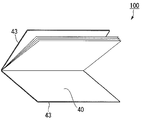
도 8a는 본 발명의 실시 형태에 따른 인레이의 평면도.
도 8b는 본 발명의 실시 형태에 따른 인레이의 정면도.
도 9a는 본 발명의 실시 형태에 따른 안테나 시트의 제조 방법을 설명하는 평면도.
도 9b는 본 발명의 실시 형태에 따른 IC 모듈의 제조 방법을 설명하는 평면도.
도 10은 본 발명의 실시 형태에 따른 인레이의 제조 방법을 설명하는 평면도.
도 11은 본 발명의 실시 형태에 따른 전자 패스포트의 개략 구성을 도시하는 사시도.
도 12는 본 발명의 실시 형태에 따른 안테나 시트의 변형예를 도시하는 평면도.
도 13은 본 발명의 제4 실시 형태의 비접촉형 정보 매체가 부착된 책자체를 도시하는 도면.
도 14는 동 비접촉형 정보 매체의 IC 인렛의 원형을 도시하는 도면.
도 15는 동 책자체(101)에 부착된 동 비접촉형 정보 매체의 단면도.
도 16은 동 비접촉형 정보 매체의 제조 시에서, 동 IC 인렛을 커트한 상태를 도시하는 도면.
도 17은 실시예에서의 동 비접촉형 정보 매체의 각 부의 치수를 도시하는 도면.
도 18a는 본 발명의 변형예의 비접촉형 정보 매체에서의 IC 인렛을 도시하는 도면.
도 18b는 본 발명의 변형예의 비접촉형 정보 매체에서의 IC 인렛을 도시하는 도면.
| 접착제 | 도포 두께 | 실험 1 | 실험 2 |
| EMAA계 열가소성 접착제 | 4㎛ | C | 1분 |
| EMAA계 열가소성 접착제 | 8㎛ | C | 2분 |
| EMAA계 열가소성 접착제 | 12㎛ | B | 4분 |
| EMAA계 열가소성 접착제+에폭시계 가교제 1% | 4㎛ | B | 3분 |
| EMAA계 열가소성 접착제+에폭시계 가교제 5% | 4㎛ | A | 10분 |
| 아크릴계 열가소성 접착제 | 4㎛ | B | 3분 |
| 아크릴계 열가소성 접착제 | 8㎛ | A | 8분 |
2 : 기판
4 : 안테나 코일
7 : 개구부
8, 9 : 안테나 접속 랜드(접속부)
12, 13 : 보강용 패턴(보강부)
18 : 슬릿 구멍
19B, 19C, 19D : 관통 구멍
20 : IC 모듈
22 : IC 칩
25 : 안테나 랜드(단자부)
30 : 인렛
40 : 인레이
41, 42 : 기재
100 : 전자 패스포트(커버를 갖는 인레이ㆍ비접촉형 IC를 갖는 데이터 캐리어)
101, 101A : 책자체
110, 110A : 비접촉형 정보 매체
112 : 시트
112A : 관통 구멍
113 : 안테나 코일
114 : IC 칩
115 : 다공질성 기재
116 : 접착제(내염화물 이온층)
W1, W2, W3, W4 : 폭
L, L3, L4 : 길이
Claims (7)
- 가요성을 갖는 기판과,
IC 칩을 구비한 외부의 IC 모듈의 단자부에 접속되며 상기 기판상에 형성되는 안테나 코일과,
상기 안테나 코일을 피복하도록 형성된 내염화물 이온층을 구비하고,
상기 기판에는 상기 IC 모듈의 적어도 일부를 수용하는 수용부가 형성되어 있는 것을 특징으로 하는, 안테나 시트. - 제1항에 있어서,
상기 내염화물 이온층은, EMAA(에틸렌메타크릴산 공중합체)계 열가소성 접착제에 에폭시계 가교제를 첨가한 물질로 된 것을 특징으로 하는, 안테나 시트 - 제2항에 있어서,
상기 EMAA계 열가소성 접착제에, 상기 에폭시계 가교제가 5% 이상 첨가된 것을 특징으로 하는, 안테나 시트. - 제1항에 있어서,
상기 내염화물 이온층이, 아크릴계 열가소성 접착제로 이루어지는 것을 특징으로 하는, 안테나 시트. - 제4항에 있어서,
상기 아크릴계 열가소성 접착제의 도포 두께가, 8㎛ 이상인 것을 특징으로 하는, 안테나 시트. - 가요성을 갖는 기판과, 상기 기판상에 형성되는 안테나 코일을 구비하고,
상기 기판에는 IC 모듈의 적어도 일부를 수용하는 수용부가 형성되어 있는 안테나 시트와,
상기 안테나 코일을 피복하도록 형성된 내염화물 이온층과,
IC 칩과 단자부를 구비하는 IC 모듈
을 갖고,
상기 IC 모듈은 상기 안테나 시트에 고정되고,
상기 안테나 시트는 상기 IC 모듈의 상기 단자부에 접속되는 것을 특징으로 하는, 트랜스폰더. - 가요성을 갖는 기판과, 상기 기판상에 형성되는 안테나 코일을 구비하고,
상기 기판에는 IC 모듈의 적어도 일부를 수용하는 수용부가 형성되어 있는 안테나 시트와,
상기 안테나 코일을 피복하도록 형성된 내염화물 이온층과,
IC 칩과 단자부를 구비하는 IC 모듈과,
상기 안테나 시트 및 상기 IC 모듈을 협지하는 한쌍의 기재를 갖고,
상기 IC 모듈은 상기 안테나 시트에 고정되고,
상기 안테나 시트는 상기 IC 모듈의 상기 단자부에 접속되는 것을 특징으로 하는, 책자체.
Applications Claiming Priority (5)
| Application Number | Priority Date | Filing Date | Title |
|---|---|---|---|
| JP2007239982 | 2007-09-14 | ||
| JPJP-P-2007-239982 | 2007-09-14 | ||
| JP2008187007 | 2008-07-18 | ||
| JPJP-P-2008-187007 | 2008-07-18 | ||
| PCT/JP2008/066570 WO2009035094A1 (ja) | 2007-09-14 | 2008-09-12 | アンテナシート、トランスポンダ及び冊子体 |
Related Parent Applications (1)
| Application Number | Title | Priority Date | Filing Date |
|---|---|---|---|
| KR1020107006003A Division KR101163300B1 (ko) | 2007-09-14 | 2008-09-12 | 안테나 시트, 트랜스폰더 및 책자체 |
Publications (2)
| Publication Number | Publication Date |
|---|---|
| KR20120029484A KR20120029484A (ko) | 2012-03-26 |
| KR101237107B1 true KR101237107B1 (ko) | 2013-02-25 |
Family
ID=40452100
Family Applications (2)
| Application Number | Title | Priority Date | Filing Date |
|---|---|---|---|
| KR1020127006038A Expired - Fee Related KR101237107B1 (ko) | 2007-09-14 | 2008-09-12 | 안테나 시트, 트랜스폰더 및 책자체 |
| KR1020107006003A Expired - Fee Related KR101163300B1 (ko) | 2007-09-14 | 2008-09-12 | 안테나 시트, 트랜스폰더 및 책자체 |
Family Applications After (1)
| Application Number | Title | Priority Date | Filing Date |
|---|---|---|---|
| KR1020107006003A Expired - Fee Related KR101163300B1 (ko) | 2007-09-14 | 2008-09-12 | 안테나 시트, 트랜스폰더 및 책자체 |
Country Status (15)
| Country | Link |
|---|---|
| US (1) | US8519905B2 (ko) |
| EP (2) | EP2192530B1 (ko) |
| JP (1) | JP5370154B2 (ko) |
| KR (2) | KR101237107B1 (ko) |
| CN (1) | CN101836225B (ko) |
| AU (1) | AU2008297839B2 (ko) |
| BR (1) | BRPI0817336A2 (ko) |
| CA (1) | CA2699552C (ko) |
| ES (2) | ES2563451T3 (ko) |
| MX (1) | MX2010002872A (ko) |
| MY (1) | MY159909A (ko) |
| PL (2) | PL2602747T3 (ko) |
| RU (1) | RU2471232C2 (ko) |
| TW (1) | TWI379241B (ko) |
| WO (1) | WO2009035094A1 (ko) |
Families Citing this family (38)
| Publication number | Priority date | Publication date | Assignee | Title |
|---|---|---|---|---|
| CA2712602C (en) * | 2008-02-22 | 2014-08-05 | Toppan Printing Co., Ltd. | Transponder and booklet |
| JP2010257416A (ja) * | 2009-04-28 | 2010-11-11 | Toppan Printing Co Ltd | 情報記録媒体、非接触型ic付データキャリア、および情報記録媒体の製造方法 |
| EP2889811B1 (en) * | 2009-04-28 | 2020-04-15 | Toppan Printing Co., Ltd. | Antenna sheet, data carrier with non-contact IC, and method for manufacturing antenna sheet |
| DE102009023715A1 (de) * | 2009-06-03 | 2010-12-09 | Leonhard Kurz Stiftung & Co. Kg | Sicherheitsdokument |
| KR101667084B1 (ko) * | 2009-08-26 | 2016-10-17 | 도판 인사츠 가부시키가이샤 | 비접촉 통신 매체 |
| JP5428761B2 (ja) * | 2009-10-30 | 2014-02-26 | 凸版印刷株式会社 | アンテナシート、トランスポンダ及び冊子体 |
| JP5397193B2 (ja) * | 2009-11-30 | 2014-01-22 | 凸版印刷株式会社 | 非接触型情報媒体と非接触型情報媒体付属冊子 |
| JP2011237969A (ja) * | 2010-05-10 | 2011-11-24 | Toppan Printing Co Ltd | 非接触型情報媒体及びこれを内蔵した冊子 |
| JP2012037957A (ja) * | 2010-08-04 | 2012-02-23 | Nippon Signal Co Ltd:The | リーダライタ及びドア開閉装置 |
| JP2012073725A (ja) * | 2010-09-28 | 2012-04-12 | Toppan Printing Co Ltd | 非接触通信媒体、冊子及びその製造方法 |
| EP2461275A1 (en) * | 2010-12-02 | 2012-06-06 | Gemalto SA | Security Document and method of manufacturing security document |
| JP2012160108A (ja) * | 2011-02-02 | 2012-08-23 | Toppan Printing Co Ltd | 非接触型情報記録媒体 |
| JP5834585B2 (ja) * | 2011-07-25 | 2015-12-24 | 凸版印刷株式会社 | 非接触通信媒体及びその製造方法 |
| TWI453677B (zh) * | 2011-12-01 | 2014-09-21 | Mutual Pak Technology Co Ltd | 射頻識別標籤與具有其之衣物 |
| US8763914B2 (en) * | 2012-01-17 | 2014-07-01 | On Track Innovations Ltd. | Decoupled contactless bi-directional systems and methods |
| WO2013161781A1 (ja) * | 2012-04-24 | 2013-10-31 | 凸版印刷株式会社 | 非接触型情報媒体及び非接触型情報媒体付属冊子 |
| US9093756B2 (en) * | 2012-09-18 | 2015-07-28 | Panasonic Intellectual Property Management Co., Ltd. | Antenna, transmitter device, receiver device, three-dimensional integrated circuit, and contactless communication system |
| FR3001070B1 (fr) * | 2013-01-17 | 2016-05-06 | Inside Secure | Systeme d'antenne pour microcircuit sans contact |
| US10909440B2 (en) * | 2013-08-22 | 2021-02-02 | Texas Instruments Incorporated | RFID tag with integrated antenna |
| FR3013152A1 (fr) * | 2013-11-14 | 2015-05-15 | Smart Packaging Solutions | Antenne double face pour carte a puce |
| WO2015085064A1 (en) * | 2013-12-05 | 2015-06-11 | Uniqarta, Inc. | Electronic device incorporated into a sheet |
| US11514288B2 (en) * | 2014-08-10 | 2022-11-29 | Amatech Group Limited | Contactless metal card constructions |
| US10977540B2 (en) | 2016-07-27 | 2021-04-13 | Composecure, Llc | RFID device |
| US11267172B2 (en) | 2016-07-27 | 2022-03-08 | Composecure, Llc | Overmolded electronic components for transaction cards and methods of making thereof |
| US11618191B2 (en) | 2016-07-27 | 2023-04-04 | Composecure, Llc | DI metal transaction devices and processes for the manufacture thereof |
| US10762412B2 (en) | 2018-01-30 | 2020-09-01 | Composecure, Llc | DI capacitive embedded metal card |
| CN106909962A (zh) * | 2017-02-08 | 2017-06-30 | 珠海恒冠宇科技有限公司 | 柔性接触式ic本证、读写机具及旧设备升级办法 |
| CN113346221B (zh) * | 2017-03-30 | 2024-03-19 | 住友电气工业株式会社 | 无线模块 |
| WO2019045638A1 (en) * | 2017-08-28 | 2019-03-07 | Smartflex Technology Pte Ltd | INTEGRATED CIRCUIT MODULES AND INTELLIGENT CARDS INCORPORATING THEM |
| SG11202002064SA (en) | 2017-09-07 | 2020-04-29 | Composecure Llc | Transaction card with embedded electronic components and process for manufacture |
| US11151437B2 (en) | 2017-09-07 | 2021-10-19 | Composecure, Llc | Metal, ceramic, or ceramic-coated transaction card with window or window pattern and optional backlighting |
| HUE060022T2 (hu) | 2017-10-18 | 2023-01-28 | Composecure Llc | Fém, kerámia vagy kerámiabevonatos tranzakciókártya ablakkal vagy ablakmintával és opcionális háttévilágítással |
| KR102129590B1 (ko) * | 2019-06-13 | 2020-07-02 | 신혜중 | 하이브리드형 무선충전용 수신안테나 장치 및 그 제조방법 |
| JP7426693B2 (ja) * | 2019-12-13 | 2024-02-02 | 日本パッケージ・システム株式会社 | Rfidインレイ |
| USD1032613S1 (en) * | 2020-02-02 | 2024-06-25 | Federal Card Services, LLC | Smart card |
| USD948613S1 (en) | 2020-04-27 | 2022-04-12 | Composecure, Llc | Layer of a transaction card |
| JP7095825B1 (ja) | 2022-03-30 | 2022-07-05 | 豊田合成株式会社 | 車両用外装部品 |
| CN115424832B (zh) * | 2022-09-05 | 2025-09-12 | 京东方科技集团股份有限公司 | 线圈结构及电子设备 |
Citations (3)
| Publication number | Priority date | Publication date | Assignee | Title |
|---|---|---|---|---|
| JP2004521429A (ja) | 2001-06-14 | 2004-07-15 | アエスカ エス.ア. | 繊維質材料製アンテナ支持体及びチップ支持体を有するコンタクトレス・スマートカード |
| JP2004280503A (ja) | 2003-03-17 | 2004-10-07 | Toppan Printing Co Ltd | コンビネーションicカード |
| JP2006155224A (ja) | 2004-11-29 | 2006-06-15 | Mitsubishi Polyester Film Copp | Rfidタグ用ポリエステルフィルム |
Family Cites Families (28)
| Publication number | Priority date | Publication date | Assignee | Title |
|---|---|---|---|---|
| KR100355209B1 (ko) * | 1994-09-22 | 2003-02-11 | 로무 가부시키가이샤 | 비접촉형ic카드및그제조방법 |
| JPH09109577A (ja) * | 1995-10-13 | 1997-04-28 | Toppan Printing Co Ltd | 非接触記憶媒体を有するカードおよびその製造方法 |
| CA2245775C (en) | 1996-02-12 | 2004-04-06 | David Finn | Method and device for bonding a wire conductor |
| TW297501U (en) | 1996-06-22 | 1997-02-01 | yun-rong Xue | Finned-pipe type evaporating device utilizing hot air to defrost |
| US5708419A (en) * | 1996-07-22 | 1998-01-13 | Checkpoint Systems, Inc. | Method of wire bonding an integrated circuit to an ultraflexible substrate |
| US6157344A (en) * | 1999-02-05 | 2000-12-05 | Xertex Technologies, Inc. | Flat panel antenna |
| US6353420B1 (en) * | 1999-04-28 | 2002-03-05 | Amerasia International Technology, Inc. | Wireless article including a plural-turn loop antenna |
| JP2002042068A (ja) | 2000-07-21 | 2002-02-08 | Dainippon Printing Co Ltd | 非接触型データキャリア及び非接触型データキャリアを有する冊子 |
| JP2002109502A (ja) * | 2000-07-28 | 2002-04-12 | Oji Paper Co Ltd | Ic実装体とその製造方法 |
| WO2002089338A2 (en) | 2001-04-30 | 2002-11-07 | Bnc Ip Switzerland Gmbh | Selective metal removal process for metallized retro-reflective and holographic films and radio frequency devices made therewith |
| KR20040037127A (ko) * | 2001-09-28 | 2004-05-04 | 미쓰비시 마테리알 가부시키가이샤 | 안테나 코일 및 그것을 이용한 rfid 용 태그,트랜스폰더용 안테나 |
| JP3881366B2 (ja) | 2002-12-06 | 2007-02-14 | 株式会社フジクラ | アンテナ |
| US7090606B2 (en) | 2003-07-03 | 2006-08-15 | The Gates Corporation | Adjustable tensioner |
| JP2005084757A (ja) * | 2003-09-04 | 2005-03-31 | Seiko Epson Corp | 無線通信icデバイス付き名刺 |
| JPWO2005045919A1 (ja) | 2003-11-11 | 2007-05-24 | 東レエンジニアリング株式会社 | 非接触idカード及びその製造方法 |
| US8136735B2 (en) * | 2004-01-23 | 2012-03-20 | Semiconductor Energy Laboratory Co., Ltd. | ID label, ID card, and ID tag |
| US7083083B2 (en) * | 2004-04-27 | 2006-08-01 | Nagraid S.A. | Portable information carrier with transponders |
| JP2008504988A (ja) * | 2004-06-29 | 2008-02-21 | カンザキ スペシャルテー ペーパーズ インコーポレテッド | 多機能の直接熱記録体 |
| WO2006077732A1 (ja) * | 2005-01-18 | 2006-07-27 | Konica Minolta Medical & Graphic, Inc. | 印刷版材料、製版方法、印刷方法、平版印刷版材料集合体用包装体、平版印刷版材料の集合体及び製版印刷方法 |
| FR2882174B1 (fr) * | 2005-02-11 | 2007-09-07 | Smart Packaging Solutions Sps | Procede de fabrication d'un dispositif microelectronique a fonctionnement sans contact notamment pour passeport electronique |
| RU2286600C1 (ru) * | 2005-05-18 | 2006-10-27 | Государственное образовательное учреждение высшего профессионального образования Московский государственный институт электронной техники (технический университет) | Электронный модуль бесконтактной индентификации |
| JP5352045B2 (ja) * | 2005-06-03 | 2013-11-27 | 株式会社半導体エネルギー研究所 | 集積回路装置の作製方法 |
| US7545276B2 (en) * | 2005-09-13 | 2009-06-09 | Semiconductor Energy Laboratory Co., Ltd. | Semiconductor device |
| TW200713074A (en) | 2005-09-26 | 2007-04-01 | Ind Tech Res Inst | Flexible RFID label and manufacturing method thereof |
| TWI297501B (en) | 2006-03-17 | 2008-06-01 | Elite Semiconductor Esmt | Method and apparatus for determining sensing timing of flash memory |
| TWM305942U (en) | 2006-05-25 | 2007-02-01 | Sunbest Technology Co Ltd | Radio frequency identification clothing tag |
| JP4855880B2 (ja) * | 2006-09-20 | 2012-01-18 | リンテック株式会社 | アンテナ回路、アンテナ回路の製造方法、icインレット、icタグ |
| US7581308B2 (en) * | 2007-01-01 | 2009-09-01 | Advanced Microelectronic And Automation Technology Ltd. | Methods of connecting an antenna to a transponder chip |
-
2008
- 2008-09-12 KR KR1020127006038A patent/KR101237107B1/ko not_active Expired - Fee Related
- 2008-09-12 AU AU2008297839A patent/AU2008297839B2/en not_active Ceased
- 2008-09-12 KR KR1020107006003A patent/KR101163300B1/ko not_active Expired - Fee Related
- 2008-09-12 PL PL13155292T patent/PL2602747T3/pl unknown
- 2008-09-12 MY MYPI2010001110A patent/MY159909A/en unknown
- 2008-09-12 CN CN2008801124273A patent/CN101836225B/zh not_active Expired - Fee Related
- 2008-09-12 EP EP08830775A patent/EP2192530B1/en active Active
- 2008-09-12 TW TW097134957A patent/TWI379241B/zh not_active IP Right Cessation
- 2008-09-12 CA CA2699552A patent/CA2699552C/en not_active Expired - Fee Related
- 2008-09-12 EP EP13155292.9A patent/EP2602747B1/en active Active
- 2008-09-12 BR BRPI0817336-2A patent/BRPI0817336A2/pt not_active Application Discontinuation
- 2008-09-12 MX MX2010002872A patent/MX2010002872A/es active IP Right Grant
- 2008-09-12 ES ES13155292.9T patent/ES2563451T3/es active Active
- 2008-09-12 PL PL08830775T patent/PL2192530T3/pl unknown
- 2008-09-12 ES ES08830775T patent/ES2415364T3/es active Active
- 2008-09-12 JP JP2009532247A patent/JP5370154B2/ja active Active
- 2008-09-12 RU RU2010109058/08A patent/RU2471232C2/ru not_active IP Right Cessation
- 2008-09-12 US US12/733,666 patent/US8519905B2/en active Active
- 2008-09-12 WO PCT/JP2008/066570 patent/WO2009035094A1/ja not_active Ceased
Patent Citations (3)
| Publication number | Priority date | Publication date | Assignee | Title |
|---|---|---|---|---|
| JP2004521429A (ja) | 2001-06-14 | 2004-07-15 | アエスカ エス.ア. | 繊維質材料製アンテナ支持体及びチップ支持体を有するコンタクトレス・スマートカード |
| JP2004280503A (ja) | 2003-03-17 | 2004-10-07 | Toppan Printing Co Ltd | コンビネーションicカード |
| JP2006155224A (ja) | 2004-11-29 | 2006-06-15 | Mitsubishi Polyester Film Copp | Rfidタグ用ポリエステルフィルム |
Also Published As
| Publication number | Publication date |
|---|---|
| CN101836225A (zh) | 2010-09-15 |
| CA2699552A1 (en) | 2009-03-19 |
| MY159909A (en) | 2017-02-15 |
| CN101836225B (zh) | 2013-10-09 |
| JP5370154B2 (ja) | 2013-12-18 |
| US20100277382A1 (en) | 2010-11-04 |
| AU2008297839B2 (en) | 2011-10-27 |
| PL2192530T3 (pl) | 2013-08-30 |
| JPWO2009035094A1 (ja) | 2010-12-24 |
| ES2563451T3 (es) | 2016-03-15 |
| ES2415364T3 (es) | 2013-07-25 |
| WO2009035094A1 (ja) | 2009-03-19 |
| EP2192530A4 (en) | 2010-10-27 |
| CA2699552C (en) | 2013-05-28 |
| EP2602747A2 (en) | 2013-06-12 |
| TW200937302A (en) | 2009-09-01 |
| EP2602747A3 (en) | 2014-07-30 |
| TWI379241B (en) | 2012-12-11 |
| KR20120029484A (ko) | 2012-03-26 |
| EP2192530A1 (en) | 2010-06-02 |
| EP2192530B1 (en) | 2013-03-27 |
| RU2010109058A (ru) | 2011-09-20 |
| US8519905B2 (en) | 2013-08-27 |
| BRPI0817336A2 (pt) | 2015-03-24 |
| EP2602747B1 (en) | 2016-01-13 |
| KR101163300B1 (ko) | 2012-07-05 |
| MX2010002872A (es) | 2010-04-09 |
| KR20100047320A (ko) | 2010-05-07 |
| AU2008297839A1 (en) | 2009-03-19 |
| PL2602747T3 (pl) | 2016-06-30 |
| RU2471232C2 (ru) | 2012-12-27 |
Similar Documents
| Publication | Publication Date | Title |
|---|---|---|
| KR101237107B1 (ko) | 안테나 시트, 트랜스폰더 및 책자체 | |
| KR101154170B1 (ko) | 트랜스폰더 및 책자체 | |
| JP5130887B2 (ja) | 非接触icインレット、カバー付き非接触icインレット、非接触icインレット付き冊子、及びこれらの製造方法 | |
| KR101027592B1 (ko) | Ic카드 및 그 제조 방법 | |
| EP1498843B1 (en) | Communication medium capable of carrying out contactless communication and method of producing the same | |
| JP2010257416A (ja) | 情報記録媒体、非接触型ic付データキャリア、および情報記録媒体の製造方法 | |
| JP2011237969A (ja) | 非接触型情報媒体及びこれを内蔵した冊子 | |
| JP2012137807A (ja) | Ic付冊子及びその製造方法 | |
| JP6281226B2 (ja) | 非接触型情報媒体および非接触型情報媒体付属冊子 | |
| JP5397193B2 (ja) | 非接触型情報媒体と非接触型情報媒体付属冊子 | |
| JP2010117833A (ja) | インレイ及びその製造方法並びに非接触型情報媒体 | |
| JP2012083820A (ja) | 非接触型情報媒体及び非接触型情報媒体付属冊子 |
Legal Events
| Date | Code | Title | Description |
|---|---|---|---|
| A107 | Divisional application of patent | ||
| PA0104 | Divisional application for international application |
St.27 status event code: A-0-1-A10-A18-div-PA0104 St.27 status event code: A-0-1-A10-A16-div-PA0104 |
|
| PG1501 | Laying open of application |
St.27 status event code: A-1-1-Q10-Q12-nap-PG1501 |
|
| A201 | Request for examination | ||
| PA0201 | Request for examination |
St.27 status event code: A-1-2-D10-D11-exm-PA0201 |
|
| E701 | Decision to grant or registration of patent right | ||
| PE0701 | Decision of registration |
St.27 status event code: A-1-2-D10-D22-exm-PE0701 |
|
| GRNT | Written decision to grant | ||
| PR0701 | Registration of establishment |
St.27 status event code: A-2-4-F10-F11-exm-PR0701 |
|
| PR1002 | Payment of registration fee |
St.27 status event code: A-2-2-U10-U12-oth-PR1002 Fee payment year number: 1 |
|
| PG1601 | Publication of registration |
St.27 status event code: A-4-4-Q10-Q13-nap-PG1601 |
|
| P14-X000 | Amendment of ip right document requested |
St.27 status event code: A-5-5-P10-P14-nap-X000 |
|
| P16-X000 | Ip right document amended |
St.27 status event code: A-5-5-P10-P16-nap-X000 |
|
| Q16-X000 | A copy of ip right certificate issued |
St.27 status event code: A-4-4-Q10-Q16-nap-X000 |
|
| FPAY | Annual fee payment |
Payment date: 20160126 Year of fee payment: 4 |
|
| PR1001 | Payment of annual fee |
St.27 status event code: A-4-4-U10-U11-oth-PR1001 Fee payment year number: 4 |
|
| FPAY | Annual fee payment |
Payment date: 20170119 Year of fee payment: 5 |
|
| PR1001 | Payment of annual fee |
St.27 status event code: A-4-4-U10-U11-oth-PR1001 Fee payment year number: 5 |
|
| FPAY | Annual fee payment |
Payment date: 20180118 Year of fee payment: 6 |
|
| PR1001 | Payment of annual fee |
St.27 status event code: A-4-4-U10-U11-oth-PR1001 Fee payment year number: 6 |
|
| FPAY | Annual fee payment |
Payment date: 20190116 Year of fee payment: 7 |
|
| PR1001 | Payment of annual fee |
St.27 status event code: A-4-4-U10-U11-oth-PR1001 Fee payment year number: 7 |
|
| FPAY | Annual fee payment |
Payment date: 20200205 Year of fee payment: 8 |
|
| PR1001 | Payment of annual fee |
St.27 status event code: A-4-4-U10-U11-oth-PR1001 Fee payment year number: 8 |
|
| PR1001 | Payment of annual fee |
St.27 status event code: A-4-4-U10-U11-oth-PR1001 Fee payment year number: 9 |
|
| PN2301 | Change of applicant |
St.27 status event code: A-5-5-R10-R13-asn-PN2301 St.27 status event code: A-5-5-R10-R11-asn-PN2301 |
|
| PR1001 | Payment of annual fee |
St.27 status event code: A-4-4-U10-U11-oth-PR1001 Fee payment year number: 10 |
|
| PR1001 | Payment of annual fee |
St.27 status event code: A-4-4-U10-U11-oth-PR1001 Fee payment year number: 11 |
|
| PR1001 | Payment of annual fee |
St.27 status event code: A-4-4-U10-U11-oth-PR1001 Fee payment year number: 12 |
|
| PN2301 | Change of applicant |
St.27 status event code: A-5-5-R10-R13-asn-PN2301 St.27 status event code: A-5-5-R10-R11-asn-PN2301 |
|
| PC1903 | Unpaid annual fee |
St.27 status event code: A-4-4-U10-U13-oth-PC1903 Not in force date: 20250220 Payment event data comment text: Termination Category : DEFAULT_OF_REGISTRATION_FEE |
|
| H13 | Ip right lapsed |
Free format text: ST27 STATUS EVENT CODE: N-4-6-H10-H13-OTH-PC1903 (AS PROVIDED BY THE NATIONAL OFFICE); TERMINATION CATEGORY : DEFAULT_OF_REGISTRATION_FEE Effective date: 20250220 |
|
| PC1903 | Unpaid annual fee |
St.27 status event code: N-4-6-H10-H13-oth-PC1903 Ip right cessation event data comment text: Termination Category : DEFAULT_OF_REGISTRATION_FEE Not in force date: 20250220 |