KR101228306B1 - Apparatus and method for removing electronic devices from substrate - Google Patents
Apparatus and method for removing electronic devices from substrate Download PDFInfo
- Publication number
- KR101228306B1 KR101228306B1 KR1020110112880A KR20110112880A KR101228306B1 KR 101228306 B1 KR101228306 B1 KR 101228306B1 KR 1020110112880 A KR1020110112880 A KR 1020110112880A KR 20110112880 A KR20110112880 A KR 20110112880A KR 101228306 B1 KR101228306 B1 KR 101228306B1
- Authority
- KR
- South Korea
- Prior art keywords
- circuit element
- vacuum
- circuit
- substrate
- light
- Prior art date
- Legal status (The legal status is an assumption and is not a legal conclusion. Google has not performed a legal analysis and makes no representation as to the accuracy of the status listed.)
- Expired - Fee Related
Links
Images


Classifications
-
- H—ELECTRICITY
- H05—ELECTRIC TECHNIQUES NOT OTHERWISE PROVIDED FOR
- H05K—PRINTED CIRCUITS; CASINGS OR CONSTRUCTIONAL DETAILS OF ELECTRIC APPARATUS; MANUFACTURE OF ASSEMBLAGES OF ELECTRICAL COMPONENTS
- H05K13/00—Apparatus or processes specially adapted for manufacturing or adjusting assemblages of electric components
- H05K13/04—Mounting of components, e.g. of leadless components
- H05K13/0486—Replacement and removal of components
-
- B—PERFORMING OPERATIONS; TRANSPORTING
- B23—MACHINE TOOLS; METAL-WORKING NOT OTHERWISE PROVIDED FOR
- B23K—SOLDERING OR UNSOLDERING; WELDING; CLADDING OR PLATING BY SOLDERING OR WELDING; CUTTING BY APPLYING HEAT LOCALLY, e.g. FLAME CUTTING; WORKING BY LASER BEAM
- B23K26/00—Working by laser beam, e.g. welding, cutting or boring
- B23K26/02—Positioning or observing the workpiece, e.g. with respect to the point of impact; Aligning, aiming or focusing the laser beam
- B23K26/06—Shaping the laser beam, e.g. by masks or multi-focusing
-
- H—ELECTRICITY
- H05—ELECTRIC TECHNIQUES NOT OTHERWISE PROVIDED FOR
- H05K—PRINTED CIRCUITS; CASINGS OR CONSTRUCTIONAL DETAILS OF ELECTRIC APPARATUS; MANUFACTURE OF ASSEMBLAGES OF ELECTRICAL COMPONENTS
- H05K13/00—Apparatus or processes specially adapted for manufacturing or adjusting assemblages of electric components
- H05K13/04—Mounting of components, e.g. of leadless components
- H05K13/0404—Pick-and-place heads or apparatus, e.g. with jaws
- H05K13/0408—Incorporating a pick-up tool
Landscapes
- Engineering & Computer Science (AREA)
- Physics & Mathematics (AREA)
- Optics & Photonics (AREA)
- Manufacturing & Machinery (AREA)
- Microelectronics & Electronic Packaging (AREA)
- Plasma & Fusion (AREA)
- Mechanical Engineering (AREA)
- Electric Connection Of Electric Components To Printed Circuits (AREA)
Abstract
개시된 회로소자 제거장치는, 기판에 장착된 회로소자를 제거하는 회로소자 제거장치로서, 기판이 탑재되는 스테이지와, 회로소자에 광을 조사하여 회로소자를 가열하는 광원장치와, 회로소자의 상부에 위치되어 분리된 회로소자를 흡입하는 진공 지그를 포함한다.The disclosed circuit device removing device is a circuit device removing device for removing a circuit device mounted on a substrate, comprising: a stage on which the substrate is mounted, a light source device for heating the circuit device by irradiating light to the circuit device, and an upper portion of the circuit device. And a vacuum jig for suctioning the separated circuit elements.

Description
본 발명은 회로소자 제거장치 및 방법에 관한 것으로서, 특히 광을 이용하여 회로소자를 가열하여 기판으로부터 제거하는 회로소자 제거장치 및 방법에 관한 것이다.BACKGROUND OF THE INVENTION 1. Field of the Invention The present invention relates to an apparatus and method for removing circuit elements, and more particularly to an apparatus and method for removing element from a substrate by heating the circuit element using light.
전자부품은 인쇄회로기판(PCB: Printed Circuit Board)에 다양한 회로소자를 탑재하는 공정을 통하여 제조된다. 예를 들어, 컴퓨터에 사용되는 메모리 카드는 다수의 메모리 소자를 인쇄회로기판에 실장하는 공정을 통하여 제조될 수 있다. 제조된 전자부품은 그 성능을 확인하기 위한 검수공정을 거치는데, 불량으로 판별된 전자부품은 가능한 한 재작업(rework) 공정을 통하여 양품으로 전환하는 것이 바람직하다. 이를 위하여는 불량으로 판명된 회로소자를 인쇄회로기판으로부터 제거할 필요가 있다.Electronic components are manufactured through a process of mounting various circuit elements on a printed circuit board (PCB). For example, a memory card used in a computer may be manufactured through a process of mounting a plurality of memory elements on a printed circuit board. The manufactured electronic component undergoes an inspection process for confirming its performance, and it is preferable that the electronic component determined to be defective is converted to a good product through a rework process as much as possible. For this purpose, it is necessary to remove a circuit element which is found to be defective from the printed circuit board.
종래에는 열풍을 회로소자에 공급하여 회로소자를 가열함으로써 기판과 회로소자 사이의 솔더 물질(30)을 녹여서 회로소자를 기판으로부터 분리하였다. 그러나, 열품을 이용하는 재작업 공정에서는 솔도 물질이 녹을 정도로 회로소자를 가열하는데 소요되는 시간이 길어서 재작업 공정의 생산성을 향상시키는 데에 한계가 있다. 또, 열풍은 제거된 회로소자만을 국부적으로 가열하기 어려워 주위의 다른 회로소자에까지 열 영향을 미칠 수 있다. 또, 재작업 공정의 자동화가 어려워 공정비용 및 부품단가를 증가시키는 일 요인이 될 수 있다.Conventionally, hot air is supplied to a circuit element to heat the circuit element, thereby melting the
본 발명은 회로소자를 기판으로부터 신속하고 신뢰성있게 제거할 수 있는 회로소자 제거장치 및 방법을 제공하는 것을 목적으로 한다. 또한, 본 발명은 회로소자를 기판으로부터 제거할 수 있는 자동화가 가능한 회로소자 제거장치 및 방법을 제공하는 것을 목적으로 한다. It is an object of the present invention to provide an apparatus and method for removing a circuit element which can quickly and reliably remove the circuit element from a substrate. It is also an object of the present invention to provide an apparatus and method for circuit automation removal capable of removing circuit elements from a substrate.
본 발명의 일 실시예에 따른 회로소자 제거장치는, 기판에 장착된 회로소자를 제거하는 회로소자 제거장치로서, 상기 기판이 탑재되는 스테이지; 상기 회로소자에 광을 조사하여 상기 회로소자를 가열하는 광원장치; 상기 회로소자의 상부에 위치되어 분리된 상기 회로소자를 흡착시키는 진공 지그;를 포함한다.A circuit device removing apparatus according to an embodiment of the present invention includes a circuit device removing device for removing a circuit device mounted on a substrate, comprising: a stage on which the substrate is mounted; A light source device for heating the circuit elements by irradiating light to the circuit elements; And a vacuum jig positioned on the circuit device to suck the separated circuit device.
상기 진공 지그는, 상기 회로소자에 대응되는 위치에 마련되는 관통부; 상기 관통부의 상방을 덮으며 상기 광이 상기 회로소자에 조사될 수 있도록 투광성 물질로 된 광창부재; 및 상기 관통부에 진공 흡입력을 제공하기 위한 진공 통로를 포함하는 진공 지그;를 포함할 수 있다.The vacuum jig may include a through part provided at a position corresponding to the circuit element; A light window member made of a light-transmissive material covering the upper portion of the penetrating portion so that the light can be irradiated to the circuit element; And a vacuum jig including a vacuum passage for providing a vacuum suction force to the penetrating portion.
상기 관통부의 단면은 상기 회로소자의 단면보다 작다.The cross section of the penetrating portion is smaller than the cross section of the circuit element.
분리되기 전에 상기 회로소자의 상면은 상기 진공 지그의 하면으로부터 이격되게 위치된다.The upper surface of the circuit element is positioned away from the lower surface of the vacuum jig before separation.
상기 장치는, 상기 진공 흡입력의 변화로부터 상기 회로소자가 상기 진공 지그에 흡착되었는지 여부를 검출하는 진공 검출기;를 더 구비할 수 있다. 상기 진공 검출기에 의하여 상기 회로소자가 상기 진공 지그에 흡착된 상태가 검출된 경우, 상기 광원장치는 광조사를 중지할 수 있다.The apparatus may further include a vacuum detector for detecting whether the circuit element is adsorbed to the vacuum jig from the change of the vacuum suction force. When the state in which the circuit element is adsorbed to the vacuum jig is detected by the vacuum detector, the light source device may stop light irradiation.
상기 광창부재에는 반사방지코팅층이 마련될 수 있다.An antireflection coating layer may be provided on the light window member.
상기 스테이지에는 상기 기판의 하면으로부터 상기 회로소자를 가열하는 히터가 마련될 수 있다.The stage may be provided with a heater for heating the circuit element from the lower surface of the substrate.
본 발명의 일 실시예에 따른 회로소자 제거방봅은, 회로소자가 장착된 기판을 스테이지에 탑재하는 단계; 진공 지그의 관통부를 상기 회로소자와 정렬시키고, 상기 관통부에 진공 흡입력을 제공하는 단계; 상기 관통부의 상부를 덮는 광창부재를 통하여 레이저 광을 상기 회로소자에 조사하여 상기 회로소자를 가열하여 솔더 물질(30)을 연화시키는 단계; 상기 진공 흡입력에 의하여 상기 회로소자를 상기 진공 지그에 흡착시키는 단계;를 포함한다.In accordance with another aspect of the present invention, there is provided a circuit device removal method comprising: mounting a substrate on which a circuit device is mounted on a stage; Aligning a penetrating portion of a vacuum jig with the circuit element, and providing a vacuum suction force to the penetrating portion; Irradiating laser light to the circuit device through a light window member covering an upper portion of the through part to heat the circuit device to soften the solder material (30); And adsorbing the circuit element to the vacuum jig by the vacuum suction force.
상기 관통부의 단면은 상기 회로소자의 단면보다 작다. 상기 진공 지그의 하면은 분리되기 전에 상기 회로소자의 상면으로부터 이격되게 배치된다.The cross section of the penetrating portion is smaller than the cross section of the circuit element. The lower surface of the vacuum jig is disposed apart from the upper surface of the circuit element before being separated.
상기 방법은, 진공 검출기를 이용하여 상기 진공 흡입력의 변화로부터 상기 회로소자가 상기 진공 지그에 흡착되었는지 여부를 검출하는 단계;를 더 구비할 수 있다. 상기 방법은, 상기 진공 검출기에 의하여 상기 회로소자가 상기 진공 지그에 흡착된 상태가 검출된 경우, 광조사를 중지하는 단계;를 더 구비할 수 있다. 상기 방법은, 상기 스테이지에 마련된 히터를 이용하여 상기 기판의 하면으로부터 상기 회로소자를 가열하는 단계;를 더 구비할 수 있다.The method may further include detecting whether the circuit element is adsorbed to the vacuum jig from the change of the vacuum suction force by using a vacuum detector. The method may further include stopping light irradiation when the state in which the circuit element is adsorbed to the vacuum jig by the vacuum detector is detected. The method may further include heating the circuit device from a lower surface of the substrate using a heater provided in the stage.
본 발명에 따른 회로소자 제거장치 및 방법에 따르면, 다음과 같은 효과를 얻을 수 있다. According to the circuit element removing apparatus and method according to the present invention, the following effects can be obtained.
첫째, 레이저 광을 조사하는 광원장치와 진공 지그를 채용함으로써, 회로소자를 신속하게 기판으로부터 분리할 수 있다. First, by employing a light source device and a vacuum jig for irradiating laser light, the circuit element can be quickly separated from the substrate.
둘째, 회로소자를 국부적으로 신속하게 가열할 수 있으므로, 기판 및 기판 상의 다른 회로소자에 미치는 열영향을 줄일 수 있다. Second, the circuit element can be heated locally quickly, reducing the thermal effects on the substrate and other circuit elements on the substrate.
셋째, 순간적인 가열에 의하여 회로소자를 분리하므로 분리 후에 기판 상에 잔류되는 솔더 물질(30)의 양을 줄일 수 있다. Third, since the circuit device is separated by instantaneous heating, the amount of
넷째, 적절한 가열온도에 도달되면 회로소자가 기판으로부터 분리되므로, 가열시간의 설정이나 가열온도의 모니터링이 필요없으며 과열의 위험을 줄일 수 있다. Fourth, since the circuit element is separated from the substrate when the appropriate heating temperature is reached, there is no need to set the heating time or monitor the heating temperature and reduce the risk of overheating.
다섯째, 분리된 회로소자가 자동으로 진공 지그에 흡입되므로 제거 공정의 자동화가 가능하여 공정 효율을 향상시킬 수 있다.Fifth, since the separated circuit elements are automatically sucked into the vacuum jig, automation of the removal process is possible, thereby improving process efficiency.
여섯째, 히터를 이용하여 기판의 하부로부터 열에너지를 공급함으로써 솔더 물질이 회로소자와 함께 제거되도록 할 수 있다. 따라서, 기판에 잔류되는 솔더 물질의 양을 더욱 줄일 수 있어, 재작업의 신뢰성 및 품질을 향상시킬 수 있다.Sixth, the solder material may be removed together with the circuit elements by supplying thermal energy from the lower portion of the substrate using a heater. Thus, the amount of solder material remaining on the substrate can be further reduced, thereby improving the reliability and quality of the rework.
도 1은 본 발명에 따른 회로소자 제거장치의 일 실시예의 개략적인 사시도.
도 2는 도 1에 도시된 회로소자 제거장치의 일 실시예의 단면도.
도 3은 회로소자에 광을 조사하는 광경로의 일 예를 도시한 평면도
도 4는 회로소자가 진공 지그에 흡입된 상태를 도시한 도면.1 is a schematic perspective view of one embodiment of a circuit device removing device according to the present invention;
FIG. 2 is a cross-sectional view of one embodiment of the device for removing a circuit device shown in FIG. 1. FIG.
3 is a plan view showing an example of an optical path for irradiating light to a circuit element
4 is a view showing a state in which a circuit element is sucked into a vacuum jig.
이하, 첨부된 도면들을 참조하여 본 발명에 따른 회로소자 제거장치 및 방법의 실시예들을 설명한다. Hereinafter, embodiments of an apparatus and method for removing a circuit device according to the present invention will be described with reference to the accompanying drawings.
도 1은 본 발명에 따른 회로소자 제거장치의 일 실시예의 개략적인 사시도이며, 도 2는 도 1에 도시된 회로소자 제거장치의 일 실시예의 단면도이다. 도 1을 보면, 스테이지(200)와, 진공 지그(300), 및 광원장치(100)가 개시되어 있다. 회로소자(20)가 실장된 기판(10)은 스테이지(200)에 탑재된다. 도면으로 도시되지는 않았지만, 스테이지(200)에는 회로소자(20)가 실장된 기판(10)을 고정시키기 위한 클램핑 장치가 마련될 수 있다. 기판(10)은 예를 들어 회로소자(20)로서 메모리 칩이 실장된 컴퓨터용 메모리 카드 가판일 수 있다. 다만, 본 발명의 범위가 이에 의하여 한정되는 것은 아니다. 1 is a schematic perspective view of an embodiment of a circuit device removing apparatus according to the present invention, and FIG. 2 is a cross-sectional view of an embodiment of the circuit device removing apparatus shown in FIG. 1, a
광원장치(100)는 회로소자(20)에 광(L)을 조사하여 회로소자(20)를 가열하기 위한 것이다. 회로소자(20)가 가열되면 회로소자(20)와 기판(10) 사이의 솔더 물질(30), 예를 들어 납, 구리 등의 온도가 상승하면서 연화된다. 이때, 회로소자(20)를 상방으로 들어올림으로써 회로소자(20)를 기판(10)으로부터 제거할 수 있다. 광원장치(100)는 예를 들어 높은 에너지 밀도를 가지는 레이저 광을 조사하는 레이저장치일 수 있다. 이 외에도 광(L)의 종류는 회로소자(20)를 가열할 수 있는 것이라면 특별히 제한되지 않는다.The
광원장치(100)와 회로소자(20) 사이에는 진공 지그(300)가 개재된다. 진공 지그(300)는 기판(10)으로부터 제거된 회로소자(20)를 잡을 수 있도록 구성된다. 도 1과 도 2를 참조하면, 진공 지그(300)에는 관통부(320)와 진공 통로(330)가 마련된다. 관통부(320)는 몸체(310)를 상하방향, 즉 광(L)의 진행방향으로 관통하여 형성된다. 진공 통로(330)는 진공펌프(410)와 연결된다. 이에 의하여 관통부(320) 내부에는 진공 흡입력이 제공된다. 진공 흡입력에 의하여 회로소자(20)를 흡입할 수 있도록 하기 위하여, 관통부(320)의 단면 크기는 회로소자(20)의 단면 크기보다 작다. The
광(L)은 진공 지그(300)를 통하여 회로소자(20)에 조사된다. 이를 위하여, 진공 지그(300)에는 광창부재(350)가 마련된다. 광창부재(350)는 광(L)이 투과될 수 있는 투광성 부재이다. 광창부재(350)에는 광(L)의 통과효율을 향상시키기 위하여 반사방지코팅층(360)이 마련될 수 있다. 광창부재(350)는 관통부(320)의 상측을 막는다. 이에 의하여, 관통부(320)는 회로소자(20)와 대면되는 하부만이 개방된 상태가 된다. The light L is irradiated to the
진공 검출기(420)는 관통부(320)에 제공되는 진공 흡입력의 변화를 검출한다. 진공 검출기(420)는 예를 들어 압력센서일 수 있다. 후술하는 바와 같이 진공 검출기(420)의 검출신호로부터 회로소자(20)가 기판(10)으로부터 분리되었는지 여부를 검지할 수 있다.The
스테이지(200)는 진공 지그(300)의 관통부(320)와 회로소자(20)를 정렬시키기 위하여 이동될 수 있다. 스테이지(200)는 예를 들어 평면 내에서 이동 가능한 XY스테이지일 수 있다. 또한 스테이지(200)는 일련의 순차적인 공정에 적용되기 위하여 도시되지 않은 운반수단, 예를 들어 컨베이어 벨트에 의하여 운반될 수도 있다. 도 2를 참조하면, 스테이지(200)에는 기판(10)을 가열하기 위한 히터(210)가 설치될 수 있다. 히터(210)는 예를 들어 전열기일 수 있다. 히터(210)를 이용하여 기판(10)을 하부로부터 가열하여 회로소자(20)와 기판(10)을 전기적으로 연결시키는 솔더 물질(30)의 온도를 높여 더 신속하게 회로소자(20)를 분리할 수 있다. The
진공 지그(300)는 기판(10)으로부터 분리된 회로소자(20)를 배출하기 위하여 이동될 수 있다. 또한, 진공 지그(300)는 관통부(320)와 회로소자(20)를 정렬시키기 위하여 이동될 수 있다. 진공 지그(300)는 예를 들어 회동되는 작동 아암(500)과 연결될 수 있다. 진공 지그(300)에 회로소자(20)가 분리되어 흡착된 후에 도 1에 점선으로 도시된 바와 같이 작동 아암(500)을 구동하여 진공 지그(300)를 이동시키고 진공 흡입력을 차단함으로써 회로소자(20)를 폐기부(600)에 폐기할 수 있다. 또한 진공 지그(300)는 도시되지 않은 XY이동수단에 의하여 이동될 수도 있다. 광원장치(100)는 관통부(320)와의 정렬을 위하여 진공 지그(300)와 함께 또는 독립적으로 이동될 수 있다. 또한 광원장치(100)는 회로소자(20)를 국부적으로 또는 전체적으로 가열하기 위하여 이동될 수 있다. 물론, 광원장치(100)는 고정된 위치에 위치되고, 스테이지(200) 또는 진공 지그(300)와 스테이지(200)가 함께 이동될 수도 있다.The
제어부(700)는 회로소자(20)를 제거 과정을 전체적으로 제어한다. 예를 들어 제어부(700)는 진공 검출기(420)의 검출신호에 기반하여 광원장치(100)의 온/오프 및 진공 펌프(410)의 온/오프를 제어할 수 있다. 진공 흡입력의 차단은 진공 펌프(410)를 오프시키거나 또는 밸브(430)를 구동함으로써 구현될 수 있다. 제어부(700)는 스테이지(200) 및/또는 진공 지그(300)의 이동 등을 제어할 수 있다. The controller 700 controls the removal process of the
이하에서, 상술한 바와 같은 구성에 의하여, 기판(10)으로부터 회로소자(20)를 제거하는 방법을 설명한다.Hereinafter, the method of removing the
도 2를 참조하면, 스테이지(200) 위에 회로소자(20)가 실장된 기판(10)이 탑재된다. 스테이지(200) 또는 진공 지그(300) 또는 이 둘이 이동되어 회로소자(20)와 관통부(320)를 정렬시킨다. 진공 지그(300)의 하면(311)은 회로소자(20)의 상면(21)으로부터 이격되게 위치된다. 진공 지그(300)의 하면(311)과 회로소자(20)의 상면(21) 사이의 간격(G)은 진공 흡입력을 감안하여 적절히 설정될 수 있다. 일 예로서, 간격(G)은 약 200㎛ 정도로 설정될 수 있다. 간격(G)은 기판(10)으로부터 분리된 회로소자(20)가 진공 흡입력에 의하여 흡입되어 진공 지그(300)의 하면(311)으로 흡착될 수 있도록 진공 흡입력의 크기와 회로소자(20)의 무게 등을 감안하여 적절히 설정될 수 있다. Referring to FIG. 2, the
진공펌프(410)는 진공 통로(330)를 통하여 관통부(320)에 진공 흡입력을 제공한다. 진공 지그(300)의 하면(311)이 회로소자(20)로부터 이격되어 있으므로 회로소자(20)가 기판(10)에 솔더링 된 상태에서는 회로소자(20)는 진공 지그(300) 쪽으로 흡입되지 않는다.The vacuum pump 410 provides a vacuum suction force to the through
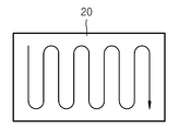
다음으로, 광원장치(100)는 광창부재(350)를 통하여 광(L)을 조사하여 회로소자(20)를 가열한다. 광원장치(100)는 회로소자(20)의 특정 부위, 예를 들어 기판(10)에 솔더링된 위치만을 국부적으로 가열할 수 있다. 광원장치(100)는 도 3에 도시된 바와 같이 지그재그 경로를 따라 회로소자(20)를 전체적으로 가열할 수도 있다. 이를 위하여, 광원장치(100) 또는 스테이지(200)가 소정의 가열경로를 따라 이동될 수 있다. 광(L)이 조사되면 회로소자(20)는 광에너지를 흡수하여 온도가 상승된다. 그러면, 기회로소자(20)와 기판(10) 사이의 솔더 물질(30)이 녹고, 회로소자(20)와 기판(10)과의 부착력이 약화된다. 회로소자(20)의 가열온도는 예를 들어 약 200℃ 내지 약 300℃ 정도일 수 있다. 광원장치(100)로서 고에너지의 레이저 광을 채용하면 매우 신속하게 회로소자(20)를 가열할 수 있다. 레이저 광을 채용하는 경우의 열풍을 사용하는 경우에 비하여 수 배 내지는 수십 배정도 빠르게 회로소자(20)를 가열할 수 있어, 공정 시간을 단축시킬 수 있다. 또한, 광(L)을 제거하고자 하는 회로소자(20)에만 조사할 수 있으므로, 기판(10) 또는 기판(10)에 실장된 다른 회로소자에 미치는 열영향을 저감시킬 수 있어, 재작업(rework)의 수율과 신뢰성을 향상시킬 수 있다. 스테이지(200)에 히터(210)를 채용하여 기판(10)을 하면으로부터 가열하는 경우에는 더 신속하게 회로소자(20)를 소망하는 가열온도에 도달시킬 수 있다.Next, the
솔더 물질(30)이 녹아서 연화되면서 회로소자(20)와 기판(10)과의 부착력이 진공 흡입력보다 약해지면, 진공 흡입력에 의하여 회로소자(20)가 기판(10)으로부터 분리되어 진공 지그(300)의 하면(311)에 흡착된다. 이와 같이 소망하는 가열온도에 도달되는 순간 회로소자(20)가 기판(10)으로부터 분리되므로, 회로소자(20)의 열에너지가 기판(10) 및 기판(10)에 실장된 다른 회로소자에 전달되는 시간을 단축시킬 수 있다. 종래의 열풍을 이용하여 회로소자(20)를 가열하는 경우에는 회로소자(20)가 소망하는 가열온도까지 가열되었는지 여부를 알기 어려워 지나치게 회로소자(20)를 가열하여 기판(10)이나 다른 회로소자의 열손상을 초래할 위험이 있었다. 그러나, 본 실시예의 제거장치 및 방법에 따르면, 회로소자(20)가 소망하는 가열온도까지 가열되는 순간 기판(10)으로부터 분리되므로 가열온도를 모니터링 할 필요없이 자동화된 공정에 의하여 회로소자(20)를 기판(10)으로부터 분리할 수 있다.When the
또한, 회로소자(20)가 매우 빠르게 가열된 후에 기판(10)으로부터 분리되므로 솔더 물질(30)의 기판(10)에의 잔류량이 매우 적다. 솔더 물질(30)이 기판(10)에 잔류하는 때에는 새로운 회로소자를 기판(10)에 실장하기 전에 잔류하는 솔더 물질(30)을 제거하는 공정이 추가되어야 하는 번거로움이 있다. 그러나, 본 발명에 따른 제거장치 및 방법에 의하면, 기판(10)에 솔더 물질(30)이 거의 잔류되지 않아 솔더 물질(30) 제거 공정에 거의 필요치 않다. 또한, 히터(210)를 이용하여 기판의 하부로부터 열에너지를 공급함으로써 솔더 물질(30)이 회로소자(20)와 함께 제거되도록 할 수 있다. 따라서, 기판(10)에 잔류되는 솔더 물질(30)의 양을 더욱 줄일 수 있어, 재작업의 신뢰성 및 품질을 향상시킬 수 있다.In addition, since the
회로소자(20)가 기판(10)으로부터 분리되었는지 여부는 진공 검출기(420)에 의하여 판별될 수 있다. 회로소자(20)가 기판(10)으로부터 분리되어 진공 지그(300)의 하면(311)에 부착되면 관통부(320)에 작용되는 진공 흡입력에 증가되므로, 진공 검출기(420)의 검출신호가 변하게 된다, 따라서, 진공 검출기(420)의 검출신호로부터 회로소자(20)가 기판(10)으로부터 분리되는 순간을 인지하고, 광원장치(100)로부터의 광 조사를 중지할 수 있으며, 이에 의하여 과열을 방지할 수 있다.Whether the
회로소자(20)가 진공 지그(300)에 흡입되면, 제어부(700)는 예를 들어 도 1에 점선으로 도시된 바와 같이 작동 아암(500)을 구동하여 진공 지그(300)를 폐기통(600)의 상부로 이동시키고, 예를 들어 밸브(430)를 작동시켜 진공 펌프(410)로부터 제공되는 진공 흡입력의 제공을 차단함으로써 제거된 회로소자(20)를 폐기통에 낙하시킬 수 있다.When the
상기한 바와 같이, 레이저 광을 조사하는 광원장치(100)와 진공 지그(300)를 채용함으로써, 회로소자(20)를 신속하게 기판(10)으로부터 분리할 수 있다. 또한, 회로소자(20)를 국부적으로 신속하게 가열할 수 있으므로, 기판(10) 및 기판(10) 상의 다른 회로소자에 미치는 열영향을 줄일 수 있다. 또한, 순간적인 가열에 의하여 회로소자(20)를 분리하므로 분리 후에 기판(10) 상에 잔류되는 솔더 물질(30)의 양을 줄일 수 있다. 또한, 적절한 가열온도에 도달되면 회로소자(20)가 기판(10)으로부터 분리되므로, 가열시간의 설정이나 가열온도의 모니터링이 필요없으며 과열의 위험을 줄일 수 있다. 또한, 분리된 회로소자(20)가 자동으로 진공 지그(300)에 흡입되므로 제거 공정의 자동화가 가능하여 공정 효율을 향상시킬 수 있다.As described above, the
상기한 실시예들은 예시적인 것에 불과한 것으로, 당해 기술분야의 통상을 지식을 가진 자라면 이로부터 다양한 변형 및 균등한 타 실시예가 가능하다. 따라서, 본 발명의 진정한 기술적 보호범위는 하기의 특허청구범위에 기재된 발명의 기술적 사상에 의해 정해져야만 할 것이다.The above embodiments are merely exemplary, and various modifications and equivalent other embodiments are possible to those skilled in the art. Accordingly, the true scope of protection of the present invention should be determined by the technical idea of the invention described in the following claims.
10...기판 20...회로소자
100...광원장치 200...스테이지
210...히터 300...진공 지그
310...몸체 320...관통부
330...진공 통로 350...광창부재
360...반사방지층 410...진공 펌프
420...진공 검출기 430...밸브
700...제어부10 ...
100
210 ...
310 ...
330
360 ... reflective layer 410 ... vacuum pump
420
700 ... control unit
Claims (14)
상기 기판이 탑재되는 스테이지;
상기 회로소자에 광을 조사하여 상기 회로소자를 가열하는 광원장치;
상기 회로소자의 상부에 위치되어 분리된 상기 회로소자를 흡착시키는 진공 지그;를 포함하며,
상기 진공 지그는,
상기 회로소자에 대응되는 위치에 마련되는 관통부;
상기 관통부의 상방을 덮으며 상기 광이 상기 회로소자에 조사될 수 있도록 투광성 물질로 된 광창부재; 및
상기 관통부에 진공 흡입력을 제공하기 위한 진공 통로;를 포함하는 회로소자 제거장치.A circuit element removing apparatus for removing circuit elements mounted on a substrate,
A stage on which the substrate is mounted;
A light source device for heating the circuit elements by irradiating light to the circuit elements;
And a vacuum jig positioned on an upper portion of the circuit element to adsorb the separated circuit element.
The vacuum jig,
A through part provided at a position corresponding to the circuit element;
A light window member made of a light-transmissive material covering the upper portion of the penetrating portion so that the light can be irradiated to the circuit element; And
And a vacuum passage for providing a vacuum suction force to the penetrating portion.
상기 관통부의 단면은 상기 회로소자의 단면보다 작은 것을 특징으로 하는 회로소자 제거장치.The method of claim 2,
And a cross section of the through part is smaller than a cross section of the circuit element.
분리되기 전에 상기 회로소자의 상면은 상기 진공 지그의 하면으로부터 이격된 것을 특징으로 하는 회로소자 제거장치.The method of claim 3,
And the upper surface of the circuit element is separated from the lower surface of the vacuum jig before separation.
상기 진공 흡입력의 변화로부터 상기 회로소자가 상기 진공 지그에 흡착되었는지 여부를 검출하는 진공 검출기;를 더 구비하는 회로소자 제거장치.5. The method according to any one of claims 2 to 4,
And a vacuum detector for detecting whether the circuit element is absorbed by the vacuum jig from the change of the vacuum suction force.
상기 진공 검출기에 의하여 상기 회로소자가 상기 진공 지그에 흡착된 상태가 검출된 경우, 상기 광원장치는 광조사를 중지하는 것을 특징으로 하는 회로소자 제거장치.The method of claim 5,
And the light source device stops light irradiation when it is detected by the vacuum detector that the circuit element is attracted to the vacuum jig.
상기 광창부재에는 반사방지코팅층이 마련된 것을 특징으로 하는 회로소자 제거장치.5. The method according to any one of claims 2 to 4,
The optical element removing device is characterized in that the anti-reflection coating layer is provided on the light window member.
상기 스테이지에는 상기 기판의 하면으로부터 상기 회로소자를 가열하는 가열수단이 마련된 것을 특징으로 하는 회로소자 제거장치.5. The method according to any one of claims 2 to 4,
And the heating means for heating the circuit element from the lower surface of the substrate.
진공 지그의 관통부를 상기 회로소자와 정렬시키고, 상기 관통부에 진공 흡입력을 제공하는 단계;
상기 관통부의 상부를 덮는 광창부재를 통하여 레이저 광을 상기 회로소자에 조사하여 상기 회로소자를 가열하여 솔더 물질을 연화시키는 단계;
상기 진공 흡입력에 의하여 상기 회로소자를 상기 진공 지그에 흡착시키는 단계;를 포함하는 회로소자 제거방법.Mounting a substrate on which a circuit element is mounted on a stage;
Aligning a penetrating portion of a vacuum jig with the circuit element, and providing a vacuum suction force to the penetrating portion;
Irradiating laser light to the circuit device through a light window member covering an upper portion of the through part to heat the circuit device to soften a solder material;
And adsorbing the circuit element to the vacuum jig by the vacuum suction force.
상기 관통부의 단면은 상기 회로소자의 단면보다 작은 것을 특징으로 하는 회로소자 제거방법.10. The method of claim 9,
And the cross section of the through part is smaller than the cross section of the circuit element.
상기 진공 지그의 하면은 분리되기 전에 상기 회로소자의 상면으로부터 이격되게 배치되는 것을 특징으로 하는 회로소자 제거방법.The method of claim 10,
And the bottom surface of the vacuum jig is spaced apart from the top surface of the circuit device before being separated.
진공 검출기를 이용하여 상기 진공 흡입력의 변화로부터 상기 회로소자가 상기 진공 지그에 흡착되었는지 여부를 검출하는 단계;를 더 구비하는 것을 특징으로 하는 회로소자 제거방법.The method of claim 11,
And detecting whether the circuit element is adsorbed to the vacuum jig from the change of the vacuum suction force by using a vacuum detector.
상기 진공 검출기에 의하여 상기 회로소자가 상기 진공 지그에 흡착된 상태가 검출된 경우, 광조사를 중지하는 단계;를 더 구비하는 것을 특징으로 하는 회로소자 제거방법.The method of claim 12,
And stopping light irradiation when the state in which the circuit element is adsorbed to the vacuum jig is detected by the vacuum detector.
상기 스테이지에 마련된 히터를 이용하여 상기 기판의 하면으로부터 상기 회로소자를 가열하는 단계;를 더 구비하는 것을 특징으로 하는 회로소자 제거방법.14. The method according to any one of claims 9 to 13,
And heating the circuit device from the bottom surface of the substrate using a heater provided in the stage.
Priority Applications (1)
| Application Number | Priority Date | Filing Date | Title |
|---|---|---|---|
| KR1020110112880A KR101228306B1 (en) | 2011-11-01 | 2011-11-01 | Apparatus and method for removing electronic devices from substrate |
Applications Claiming Priority (1)
| Application Number | Priority Date | Filing Date | Title |
|---|---|---|---|
| KR1020110112880A KR101228306B1 (en) | 2011-11-01 | 2011-11-01 | Apparatus and method for removing electronic devices from substrate |
Publications (1)
| Publication Number | Publication Date |
|---|---|
| KR101228306B1 true KR101228306B1 (en) | 2013-01-31 |
Family
ID=47842891
Family Applications (1)
| Application Number | Title | Priority Date | Filing Date |
|---|---|---|---|
| KR1020110112880A Expired - Fee Related KR101228306B1 (en) | 2011-11-01 | 2011-11-01 | Apparatus and method for removing electronic devices from substrate |
Country Status (1)
| Country | Link |
|---|---|
| KR (1) | KR101228306B1 (en) |
Cited By (7)
| Publication number | Priority date | Publication date | Assignee | Title |
|---|---|---|---|---|
| KR20180087896A (en) | 2017-01-25 | 2018-08-03 | 한국기계연구원 | Apparatus and method for repairing bad elements |
| CN109526197A (en) * | 2018-09-30 | 2019-03-26 | 武汉联特科技有限公司 | A kind of device for repairing for optics COB encapsulation |
| CN111556705A (en) * | 2019-02-11 | 2020-08-18 | 系统科技公司 | Defective light emitting diode removing device |
| CN111716006A (en) * | 2020-06-17 | 2020-09-29 | 昂纳信息技术(深圳)有限公司 | A method and system for dismantling optical components by laser |
| KR20220028883A (en) | 2020-08-31 | 2022-03-08 | 한국기계연구원 | Apparatus for repairing device |
| KR20220032415A (en) | 2020-09-07 | 2022-03-15 | 한국기계연구원 | Stamp for removing defective device and apparatus for removing defective device including the same |
| KR20220131053A (en) * | 2021-03-19 | 2022-09-27 | 참엔지니어링(주) | Repair apparatus and method |
Citations (4)
| Publication number | Priority date | Publication date | Assignee | Title |
|---|---|---|---|---|
| JPH05136557A (en) * | 1991-11-13 | 1993-06-01 | Sony Corp | Parts exchange device |
| JPH05235536A (en) * | 1992-02-20 | 1993-09-10 | Matsushita Electric Ind Co Ltd | Electronic parts correction equipment |
| JP2009164310A (en) * | 2007-12-28 | 2009-07-23 | Sharp Corp | Electronic component repair device and electronic component repair method |
| JP2010050344A (en) * | 2008-08-22 | 2010-03-04 | Fujinon Corp | Reworking device |
-
2011
- 2011-11-01 KR KR1020110112880A patent/KR101228306B1/en not_active Expired - Fee Related
Patent Citations (4)
| Publication number | Priority date | Publication date | Assignee | Title |
|---|---|---|---|---|
| JPH05136557A (en) * | 1991-11-13 | 1993-06-01 | Sony Corp | Parts exchange device |
| JPH05235536A (en) * | 1992-02-20 | 1993-09-10 | Matsushita Electric Ind Co Ltd | Electronic parts correction equipment |
| JP2009164310A (en) * | 2007-12-28 | 2009-07-23 | Sharp Corp | Electronic component repair device and electronic component repair method |
| JP2010050344A (en) * | 2008-08-22 | 2010-03-04 | Fujinon Corp | Reworking device |
Cited By (14)
| Publication number | Priority date | Publication date | Assignee | Title |
|---|---|---|---|---|
| KR20180087896A (en) | 2017-01-25 | 2018-08-03 | 한국기계연구원 | Apparatus and method for repairing bad elements |
| CN109526197A (en) * | 2018-09-30 | 2019-03-26 | 武汉联特科技有限公司 | A kind of device for repairing for optics COB encapsulation |
| CN109526197B (en) * | 2018-09-30 | 2024-06-04 | 武汉联特科技股份有限公司 | Repairing device for optical COB packaging |
| KR102167268B1 (en) * | 2019-02-11 | 2020-10-19 | (주)에스티아이 | Device for removing defective led |
| JP2020129658A (en) * | 2019-02-11 | 2020-08-27 | エスティーアイ カンパニー リミテッド | Bad LED remover |
| KR20200097929A (en) * | 2019-02-11 | 2020-08-20 | (주)에스티아이 | Device for removing defective led |
| CN111556705B (en) * | 2019-02-11 | 2021-06-29 | 系统科技公司 | Defective LED Removal Device |
| JP6995899B2 (en) | 2019-02-11 | 2022-01-17 | エスティーアイ カンパニー リミテッド | Defective LED removal device |
| CN111556705A (en) * | 2019-02-11 | 2020-08-18 | 系统科技公司 | Defective light emitting diode removing device |
| CN111716006A (en) * | 2020-06-17 | 2020-09-29 | 昂纳信息技术(深圳)有限公司 | A method and system for dismantling optical components by laser |
| KR20220028883A (en) | 2020-08-31 | 2022-03-08 | 한국기계연구원 | Apparatus for repairing device |
| KR20220032415A (en) | 2020-09-07 | 2022-03-15 | 한국기계연구원 | Stamp for removing defective device and apparatus for removing defective device including the same |
| KR20220131053A (en) * | 2021-03-19 | 2022-09-27 | 참엔지니어링(주) | Repair apparatus and method |
| KR102458870B1 (en) * | 2021-03-19 | 2022-10-26 | 참엔지니어링(주) | Repairing apparatus and method |
Similar Documents
| Publication | Publication Date | Title |
|---|---|---|
| KR101228306B1 (en) | Apparatus and method for removing electronic devices from substrate | |
| JP6977020B2 (en) | Transfer method for semiconductor devices | |
| CN114901413B (en) | Laser reflow soldering device and laser reflow soldering method | |
| KR102420160B1 (en) | Micro LED repair process | |
| TWI457976B (en) | Protective tape peeling method and device thereof | |
| KR101933549B1 (en) | apparatus for removing semiconductor chip using the laser and removal method of the same | |
| US5601229A (en) | Conductive metal ball attaching apparatus and method, and bump forming method | |
| JP7319724B2 (en) | Joining method and joining apparatus | |
| KR20140001118A (en) | Bonding device | |
| JP4372605B2 (en) | Electronic component mounting apparatus and electronic component mounting method | |
| KR101452353B1 (en) | Apparatus for Peeling Protection Film with Checking the Peeling of Protection Film | |
| KR20210000610A (en) | System and method for manufacturing a composite substrate | |
| KR102430967B1 (en) | Laser head module of laser debonding equipment | |
| KR20200032485A (en) | Hybrid reflow apparatus combining mass reflow and laser selective reflow | |
| TWI606499B (en) | Method for separating a semiconductor wafer from a foil | |
| JP2022121826A (en) | Chip component removing method and chip component removing device | |
| KR20140095301A (en) | Apparatus and method for bonding | |
| JP6412376B2 (en) | Chip-substrate bonding method, chip-substrate temporary bonding apparatus, chip mounting system | |
| KR101452963B1 (en) | Apparatus for reballing semiconductor | |
| JP4130140B2 (en) | Electronic component joining apparatus and method, and electronic component mounting apparatus | |
| KR101659311B1 (en) | Rework apparatus of bonding error die | |
| JP2009049237A (en) | ACF pasting apparatus, flat panel display manufacturing apparatus and flat panel display | |
| KR20210149980A (en) | laser debonding device | |
| TWI906583B (en) | Install system | |
| CN202180273U (en) | Automatic dismantling tool for electronic elements |
Legal Events
| Date | Code | Title | Description |
|---|---|---|---|
| A201 | Request for examination | ||
| PA0109 | Patent application |
St.27 status event code: A-0-1-A10-A12-nap-PA0109 |
|
| PA0201 | Request for examination |
St.27 status event code: A-1-2-D10-D11-exm-PA0201 |
|
| D13-X000 | Search requested |
St.27 status event code: A-1-2-D10-D13-srh-X000 |
|
| D14-X000 | Search report completed |
St.27 status event code: A-1-2-D10-D14-srh-X000 |
|
| E902 | Notification of reason for refusal | ||
| PE0902 | Notice of grounds for rejection |
St.27 status event code: A-1-2-D10-D21-exm-PE0902 |
|
| E13-X000 | Pre-grant limitation requested |
St.27 status event code: A-2-3-E10-E13-lim-X000 |
|
| P11-X000 | Amendment of application requested |
St.27 status event code: A-2-2-P10-P11-nap-X000 |
|
| P13-X000 | Application amended |
St.27 status event code: A-2-2-P10-P13-nap-X000 |
|
| E701 | Decision to grant or registration of patent right | ||
| PE0701 | Decision of registration |
St.27 status event code: A-1-2-D10-D22-exm-PE0701 |
|
| GRNT | Written decision to grant | ||
| PR0701 | Registration of establishment |
St.27 status event code: A-2-4-F10-F11-exm-PR0701 |
|
| PR1002 | Payment of registration fee |
St.27 status event code: A-2-2-U10-U11-oth-PR1002 Fee payment year number: 1 |
|
| PG1601 | Publication of registration |
St.27 status event code: A-4-4-Q10-Q13-nap-PG1601 |
|
| R18-X000 | Changes to party contact information recorded |
St.27 status event code: A-5-5-R10-R18-oth-X000 |
|
| FPAY | Annual fee payment |
Payment date: 20160114 Year of fee payment: 4 |
|
| PR1001 | Payment of annual fee |
St.27 status event code: A-4-4-U10-U11-oth-PR1001 Fee payment year number: 4 |
|
| FPAY | Annual fee payment |
Payment date: 20170109 Year of fee payment: 5 |
|
| PR1001 | Payment of annual fee |
St.27 status event code: A-4-4-U10-U11-oth-PR1001 Fee payment year number: 5 |
|
| FPAY | Annual fee payment |
Payment date: 20180108 Year of fee payment: 6 |
|
| PR1001 | Payment of annual fee |
St.27 status event code: A-4-4-U10-U11-oth-PR1001 Fee payment year number: 6 |
|
| P22-X000 | Classification modified |
St.27 status event code: A-4-4-P10-P22-nap-X000 |
|
| PR1001 | Payment of annual fee |
St.27 status event code: A-4-4-U10-U11-oth-PR1001 Fee payment year number: 7 |
|
| FPAY | Annual fee payment |
Payment date: 20200117 Year of fee payment: 8 |
|
| PR1001 | Payment of annual fee |
St.27 status event code: A-4-4-U10-U11-oth-PR1001 Fee payment year number: 8 |
|
| PC1903 | Unpaid annual fee |
St.27 status event code: A-4-4-U10-U13-oth-PC1903 Not in force date: 20210126 Payment event data comment text: Termination Category : DEFAULT_OF_REGISTRATION_FEE |
|
| PC1903 | Unpaid annual fee |
St.27 status event code: N-4-6-H10-H13-oth-PC1903 Ip right cessation event data comment text: Termination Category : DEFAULT_OF_REGISTRATION_FEE Not in force date: 20210126 |
|
| PN2301 | Change of applicant |
St.27 status event code: A-5-5-R10-R13-asn-PN2301 St.27 status event code: A-5-5-R10-R11-asn-PN2301 |
|
| R18-X000 | Changes to party contact information recorded |
St.27 status event code: A-5-5-R10-R18-oth-X000 |