KR101142314B1 - A device with at least partial packaging and method for forming - Google Patents
A device with at least partial packaging and method for forming Download PDFInfo
- Publication number
- KR101142314B1 KR101142314B1 KR1020117006445A KR20117006445A KR101142314B1 KR 101142314 B1 KR101142314 B1 KR 101142314B1 KR 1020117006445 A KR1020117006445 A KR 1020117006445A KR 20117006445 A KR20117006445 A KR 20117006445A KR 101142314 B1 KR101142314 B1 KR 101142314B1
- Authority
- KR
- South Korea
- Prior art keywords
- electrically conductive
- conductive layer
- circuit device
- layer
- reference voltage
- Prior art date
- Legal status (The legal status is an assumption and is not a legal conclusion. Google has not performed a legal analysis and makes no representation as to the accuracy of the status listed.)
- Expired - Lifetime
Links
Images


Classifications
-
- H—ELECTRICITY
- H10—SEMICONDUCTOR DEVICES; ELECTRIC SOLID-STATE DEVICES NOT OTHERWISE PROVIDED FOR
- H10W—GENERIC PACKAGES, INTERCONNECTIONS, CONNECTORS OR OTHER CONSTRUCTIONAL DETAILS OF DEVICES COVERED BY CLASS H10
- H10W74/00—Encapsulations, e.g. protective coatings
- H10W74/10—Encapsulations, e.g. protective coatings characterised by their shape or disposition
- H10W74/111—Encapsulations, e.g. protective coatings characterised by their shape or disposition the semiconductor body being completely enclosed
- H10W74/114—Encapsulations, e.g. protective coatings characterised by their shape or disposition the semiconductor body being completely enclosed by a substrate and the encapsulations
- H10W74/117—Encapsulations, e.g. protective coatings characterised by their shape or disposition the semiconductor body being completely enclosed by a substrate and the encapsulations the substrate having spherical bumps for external connection
-
- H—ELECTRICITY
- H10—SEMICONDUCTOR DEVICES; ELECTRIC SOLID-STATE DEVICES NOT OTHERWISE PROVIDED FOR
- H10W—GENERIC PACKAGES, INTERCONNECTIONS, CONNECTORS OR OTHER CONSTRUCTIONAL DETAILS OF DEVICES COVERED BY CLASS H10
- H10W70/00—Package substrates; Interposers; Redistribution layers [RDL]
- H10W70/01—Manufacture or treatment
- H10W70/05—Manufacture or treatment of insulating or insulated package substrates, or of interposers, or of redistribution layers
- H10W70/08—Manufacture or treatment of insulating or insulated package substrates, or of interposers, or of redistribution layers by depositing layers on the chip or wafer, e.g. "chip-first" RDLs
- H10W70/09—Manufacture or treatment of insulating or insulated package substrates, or of interposers, or of redistribution layers by depositing layers on the chip or wafer, e.g. "chip-first" RDLs extending onto an encapsulation that laterally surrounds the chip or wafer, e.g. fan-out wafer level package [FOWLP] RDLs
-
- H—ELECTRICITY
- H10—SEMICONDUCTOR DEVICES; ELECTRIC SOLID-STATE DEVICES NOT OTHERWISE PROVIDED FOR
- H10W—GENERIC PACKAGES, INTERCONNECTIONS, CONNECTORS OR OTHER CONSTRUCTIONAL DETAILS OF DEVICES COVERED BY CLASS H10
- H10W70/00—Package substrates; Interposers; Redistribution layers [RDL]
- H10W70/01—Manufacture or treatment
- H10W70/05—Manufacture or treatment of insulating or insulated package substrates, or of interposers, or of redistribution layers
- H10W70/093—Connecting or disconnecting other interconnections thereto or therefrom, e.g. connecting bond wires or bumps
-
- H—ELECTRICITY
- H10—SEMICONDUCTOR DEVICES; ELECTRIC SOLID-STATE DEVICES NOT OTHERWISE PROVIDED FOR
- H10W—GENERIC PACKAGES, INTERCONNECTIONS, CONNECTORS OR OTHER CONSTRUCTIONAL DETAILS OF DEVICES COVERED BY CLASS H10
- H10W70/00—Package substrates; Interposers; Redistribution layers [RDL]
- H10W70/60—Insulating or insulated package substrates; Interposers; Redistribution layers
- H10W70/611—Insulating or insulated package substrates; Interposers; Redistribution layers for connecting multiple chips together
- H10W70/614—Insulating or insulated package substrates; Interposers; Redistribution layers for connecting multiple chips together the multiple chips being integrally enclosed
-
- H—ELECTRICITY
- H10—SEMICONDUCTOR DEVICES; ELECTRIC SOLID-STATE DEVICES NOT OTHERWISE PROVIDED FOR
- H10W—GENERIC PACKAGES, INTERCONNECTIONS, CONNECTORS OR OTHER CONSTRUCTIONAL DETAILS OF DEVICES COVERED BY CLASS H10
- H10W72/00—Interconnections or connectors in packages
-
- H—ELECTRICITY
- H10—SEMICONDUCTOR DEVICES; ELECTRIC SOLID-STATE DEVICES NOT OTHERWISE PROVIDED FOR
- H10W—GENERIC PACKAGES, INTERCONNECTIONS, CONNECTORS OR OTHER CONSTRUCTIONAL DETAILS OF DEVICES COVERED BY CLASS H10
- H10W72/00—Interconnections or connectors in packages
- H10W72/01—Manufacture or treatment
- H10W72/0198—Manufacture or treatment batch processes
-
- H—ELECTRICITY
- H10—SEMICONDUCTOR DEVICES; ELECTRIC SOLID-STATE DEVICES NOT OTHERWISE PROVIDED FOR
- H10W—GENERIC PACKAGES, INTERCONNECTIONS, CONNECTORS OR OTHER CONSTRUCTIONAL DETAILS OF DEVICES COVERED BY CLASS H10
- H10W74/00—Encapsulations, e.g. protective coatings
- H10W74/01—Manufacture or treatment
- H10W74/014—Manufacture or treatment using batch processing
-
- H—ELECTRICITY
- H10—SEMICONDUCTOR DEVICES; ELECTRIC SOLID-STATE DEVICES NOT OTHERWISE PROVIDED FOR
- H10W—GENERIC PACKAGES, INTERCONNECTIONS, CONNECTORS OR OTHER CONSTRUCTIONAL DETAILS OF DEVICES COVERED BY CLASS H10
- H10W74/00—Encapsulations, e.g. protective coatings
- H10W74/01—Manufacture or treatment
- H10W74/016—Manufacture or treatment using moulds
-
- H—ELECTRICITY
- H10—SEMICONDUCTOR DEVICES; ELECTRIC SOLID-STATE DEVICES NOT OTHERWISE PROVIDED FOR
- H10W—GENERIC PACKAGES, INTERCONNECTIONS, CONNECTORS OR OTHER CONSTRUCTIONAL DETAILS OF DEVICES COVERED BY CLASS H10
- H10W74/00—Encapsulations, e.g. protective coatings
- H10W74/01—Manufacture or treatment
- H10W74/019—Manufacture or treatment using temporary auxiliary substrates
-
- H—ELECTRICITY
- H10—SEMICONDUCTOR DEVICES; ELECTRIC SOLID-STATE DEVICES NOT OTHERWISE PROVIDED FOR
- H10W—GENERIC PACKAGES, INTERCONNECTIONS, CONNECTORS OR OTHER CONSTRUCTIONAL DETAILS OF DEVICES COVERED BY CLASS H10
- H10W74/00—Encapsulations, e.g. protective coatings
- H10W74/10—Encapsulations, e.g. protective coatings characterised by their shape or disposition
- H10W74/111—Encapsulations, e.g. protective coatings characterised by their shape or disposition the semiconductor body being completely enclosed
-
- H—ELECTRICITY
- H10—SEMICONDUCTOR DEVICES; ELECTRIC SOLID-STATE DEVICES NOT OTHERWISE PROVIDED FOR
- H10W—GENERIC PACKAGES, INTERCONNECTIONS, CONNECTORS OR OTHER CONSTRUCTIONAL DETAILS OF DEVICES COVERED BY CLASS H10
- H10W90/00—Package configurations
-
- H—ELECTRICITY
- H10—SEMICONDUCTOR DEVICES; ELECTRIC SOLID-STATE DEVICES NOT OTHERWISE PROVIDED FOR
- H10W—GENERIC PACKAGES, INTERCONNECTIONS, CONNECTORS OR OTHER CONSTRUCTIONAL DETAILS OF DEVICES COVERED BY CLASS H10
- H10W70/00—Package substrates; Interposers; Redistribution layers [RDL]
- H10W70/60—Insulating or insulated package substrates; Interposers; Redistribution layers
-
- H—ELECTRICITY
- H10—SEMICONDUCTOR DEVICES; ELECTRIC SOLID-STATE DEVICES NOT OTHERWISE PROVIDED FOR
- H10W—GENERIC PACKAGES, INTERCONNECTIONS, CONNECTORS OR OTHER CONSTRUCTIONAL DETAILS OF DEVICES COVERED BY CLASS H10
- H10W72/00—Interconnections or connectors in packages
- H10W72/071—Connecting or disconnecting
- H10W72/073—Connecting or disconnecting of die-attach connectors
-
- H—ELECTRICITY
- H10—SEMICONDUCTOR DEVICES; ELECTRIC SOLID-STATE DEVICES NOT OTHERWISE PROVIDED FOR
- H10W—GENERIC PACKAGES, INTERCONNECTIONS, CONNECTORS OR OTHER CONSTRUCTIONAL DETAILS OF DEVICES COVERED BY CLASS H10
- H10W72/00—Interconnections or connectors in packages
- H10W72/20—Bump connectors, e.g. solder bumps or copper pillars; Dummy bumps; Thermal bumps
- H10W72/241—Dispositions, e.g. layouts
-
- H—ELECTRICITY
- H10—SEMICONDUCTOR DEVICES; ELECTRIC SOLID-STATE DEVICES NOT OTHERWISE PROVIDED FOR
- H10W—GENERIC PACKAGES, INTERCONNECTIONS, CONNECTORS OR OTHER CONSTRUCTIONAL DETAILS OF DEVICES COVERED BY CLASS H10
- H10W72/00—Interconnections or connectors in packages
- H10W72/90—Bond pads, in general
- H10W72/941—Dispositions of bond pads
- H10W72/9413—Dispositions of bond pads on encapsulations
-
- H—ELECTRICITY
- H10—SEMICONDUCTOR DEVICES; ELECTRIC SOLID-STATE DEVICES NOT OTHERWISE PROVIDED FOR
- H10W—GENERIC PACKAGES, INTERCONNECTIONS, CONNECTORS OR OTHER CONSTRUCTIONAL DETAILS OF DEVICES COVERED BY CLASS H10
- H10W74/00—Encapsulations, e.g. protective coatings
-
- H—ELECTRICITY
- H10—SEMICONDUCTOR DEVICES; ELECTRIC SOLID-STATE DEVICES NOT OTHERWISE PROVIDED FOR
- H10W—GENERIC PACKAGES, INTERCONNECTIONS, CONNECTORS OR OTHER CONSTRUCTIONAL DETAILS OF DEVICES COVERED BY CLASS H10
- H10W74/00—Encapsulations, e.g. protective coatings
- H10W74/10—Encapsulations, e.g. protective coatings characterised by their shape or disposition
- H10W74/131—Encapsulations, e.g. protective coatings characterised by their shape or disposition the semiconductor body being only partially enclosed
- H10W74/142—Encapsulations, e.g. protective coatings characterised by their shape or disposition the semiconductor body being only partially enclosed the encapsulations exposing the passive side of the semiconductor body
-
- H—ELECTRICITY
- H10—SEMICONDUCTOR DEVICES; ELECTRIC SOLID-STATE DEVICES NOT OTHERWISE PROVIDED FOR
- H10W—GENERIC PACKAGES, INTERCONNECTIONS, CONNECTORS OR OTHER CONSTRUCTIONAL DETAILS OF DEVICES COVERED BY CLASS H10
- H10W90/00—Package configurations
- H10W90/701—Package configurations characterised by the relative positions of pads or connectors relative to package parts
- H10W90/731—Package configurations characterised by the relative positions of pads or connectors relative to package parts of die-attach connectors
- H10W90/734—Package configurations characterised by the relative positions of pads or connectors relative to package parts of die-attach connectors between a chip and a stacked insulating package substrate, interposer or RDL
-
- H—ELECTRICITY
- H10—SEMICONDUCTOR DEVICES; ELECTRIC SOLID-STATE DEVICES NOT OTHERWISE PROVIDED FOR
- H10W—GENERIC PACKAGES, INTERCONNECTIONS, CONNECTORS OR OTHER CONSTRUCTIONAL DETAILS OF DEVICES COVERED BY CLASS H10
- H10W90/00—Package configurations
- H10W90/701—Package configurations characterised by the relative positions of pads or connectors relative to package parts
- H10W90/731—Package configurations characterised by the relative positions of pads or connectors relative to package parts of die-attach connectors
- H10W90/736—Package configurations characterised by the relative positions of pads or connectors relative to package parts of die-attach connectors between a chip and a stacked lead frame, conducting package substrate or heat sink
Landscapes
- Structures Or Materials For Encapsulating Or Coating Semiconductor Devices Or Solid State Devices (AREA)
- Shielding Devices Or Components To Electric Or Magnetic Fields (AREA)
Abstract
일 실시예에서, 회로 디바이스(15)는 도전층(10)의 개구내에 위치되고, 회로 디바이스(15)의 활성 표면이 도전층(10)과 동일 평면이도록 캡슐제(24)로 캡슐화된다. 일 실시예에서, 도전층(10)의 적어도 일 부분은 기준 전압면(예를 들어, 접지면)으로서 이용될 수 있다. 일 실시예에서, 회로 디바이스(115)의 활성 표면은 도전층(100)과 회로 디바이스(115)의 대향 표면 사이에 있도록 회로 디바이스(115)는 도전층(100)상에 위치한다. 이 실시예에서, 도전층(100)은 회로 디바이스(115)의 활성 표면을 노출시키기 위해 적어도 하나의 개구(128)를 갖는다. 캡슐제 층(24, 126, 326)은 일 실시예들에서 전기적으로 도전성일 수 있고 다른 실시예들에서 전기적으로 비-도전성일 수 있다.In one embodiment, the circuit device 15 is located in the opening of the conductive layer 10 and encapsulated in the capsule 24 such that the active surface of the circuit device 15 is coplanar with the conductive layer 10. In one embodiment, at least a portion of the conductive layer 10 may be used as a reference voltage plane (eg, ground plane). In one embodiment, the circuit device 115 is located on the conductive layer 100 such that the active surface of the circuit device 115 is between the conductive layer 100 and the opposing surface of the circuit device 115. In this embodiment, the conductive layer 100 has at least one opening 128 to expose the active surface of the circuit device 115. Capsule layer 24, 126, 326 may be electrically conductive in one embodiment and electrically non-conductive in other embodiments.
Description
본 발명은 일반적으로 회로 디바이스에 관한 것으로서, 특히 적어도 부분적인 패키징을 갖는 회로 디바이스 및 회로 디바이스를 형성하기 위한 방법에 관한 것이다.
TECHNICAL FIELD The present invention relates generally to circuit devices, and more particularly to circuit devices and methods for forming circuit devices having at least partial packaging.
전기, 광, 능동, 및 수동 (이에 제한되지 않음)을 포함하는 모든 타입의 회로 디바이스들은, 일반적으로 회로 디바이스를 보호하고, 원할 때 회로 디바이스를 외부와 커플링하도록 허용하고, 회로 디바이스의 기능적인 이용을 여전히 허용하는 반면 비용이 저렴한 형태로 패키징된다. 회로 디바이스들의 패키징 향상이 가능한 표준, 기존의 패키징 툴들 및 프로세스들을 이용하는 것은 회로 디바이스 패키징의 발달에 대한 저렴한 접근법이다.Circuit devices of all types, including but not limited to electrical, optical, active, and passive, generally protect the circuit device, allow to couple the circuit device to the outside when desired, and Packaged in low cost while still allowing for use. Using standards, existing packaging tools and processes that enable the packaging of circuit devices is an inexpensive approach to the development of circuit device packaging.
부분적으로만 패키징된 회로 디바이스들을 상업적으로 유통(transfer) 또는 판매하는 것이 보다 일반화되고 있다. 이러한 부분적으로 패키징된 회로 디바이스들은, 원하는 최종 회로를 생산하기 위해 다른 회로 디바이스들과 조합되고 최종 형태로 패키징될 수 있다.
Commercially transferring or selling only partially packaged circuit devices has become more common. These partially packaged circuit devices can be combined with other circuit devices and packaged in final form to produce the desired final circuit.
본 발명의 목적은 적어도 부분적인 패키징을 갖는 디바이스를 제공하는 것이다.
It is an object of the present invention to provide a device having at least partial packaging.
본 발명의 상기 적어도 부분적인 패키징을 갖는 디바이스는: 능동 회로를 포함하는 제 1 표면, 상기 제 1 표면과 대향하는 제 2 표면, 및 상기 제 1 및 제 2 표면들과 실질적으로 수직한 측벽 표면들을 갖는 회로 디바이스; 및 상기 회로 디바이스의 상기 측벽 표면들 및 상기 제 2 표면 위에 놓여지고, 상기 회로 디바이스의 상기 제 1 표면의 적어도 일 부분을 노출시키는 전기적 도전 캡슐제(encapsulant)를 포함하는 것을 특징으로 한다.
The device having the at least partial packaging of the present invention comprises: a first surface comprising an active circuit, a second surface opposite the first surface, and sidewall surfaces substantially perpendicular to the first and second surfaces. A circuit device having; And an electrically conductive encapsulant overlying the sidewall surfaces and the second surface of the circuit device and exposing at least a portion of the first surface of the circuit device.
본 발명으로 인하여, 적어도 부분적인 패키징을 갖는 디바이스가 제공된다.
Due to the present invention, a device having at least partial packaging is provided.
도 1 내지 4는 본 발명의 실시예에 따라 형성된 적어도 부분적인 패키징을 갖는 복수의 회로 디바이스들의 순차적인 단면도를 도시한 도면.
도 5는 본 발명의 실시예에 따라 형성된 도 4의 적어도 부분적인 패키징을 갖는 복수의 회로 디바이스들의 저면도를 도시한 도면.
도 6은 본 발명의 실시예에 따라 형성된 적어도 부분적인 패키징을 갖는 복수의 회로 디바이스들의 단면도를 도시한 도면.
도 7은 본 발명의 실시예에 따라 형성된 적어도 부분적인 패키징을 갖는 회로 디바이스의 평면도를 도시한 도면.
도 8은 본 발명의 실시예에 따라 형성된 도 7의 적어도 부분적인 패키징을 갖는 복수의 회로 디바이스의 단면도를 도시한 도면.1-4 show sequential cross-sectional views of a plurality of circuit devices having at least partial packaging formed in accordance with an embodiment of the invention.
FIG. 5 illustrates a bottom view of a plurality of circuit devices having at least partial packaging of FIG. 4 formed in accordance with an embodiment of the invention. FIG.
6 illustrates a cross-sectional view of a plurality of circuit devices having at least partial packaging formed in accordance with an embodiment of the invention.
7 shows a top view of a circuit device with at least partial packaging formed in accordance with an embodiment of the invention.
8 illustrates a cross-sectional view of a plurality of circuit devices with at least partial packaging of FIG. 7 formed in accordance with an embodiment of the invention.
본 발명은 예를 들어 설명되었고, 첨부된 도면들로 제한되지 않으며, 동일한 참조들은 유사한 요소들을 나타낸다.The present invention has been described by way of example and not by way of limitation in the figures of the accompanying drawings in which like references indicate similar elements.
당업자들은 도면들내 요소들이 간단함 및 명료함을 위해 도시되었으며 스케일링할 필요가 없음을 이해할 것이다. 예를 들어, 도면들 내 몇몇 요소들의 크기가 본 발명의 실시예들의 이해를 돕기 위해 다른 요소들과 상대적으로 과장될 수 있다.Those skilled in the art will understand that elements in the figures are shown for simplicity and clarity and do not need to be scaled. For example, the size of some of the elements in the figures may be exaggerated relative to other elements to facilitate understanding of embodiments of the present invention.
도 1은 접착층(12) 위에 위치된 전기적 도전층(10)의 단면도를 도시한다. 본 발명의 일부 실시예들에서, 지지 구조(9)는 접착층(12)을 지지하도록 이용된다. 전기적 도전층(10)과 접착층(12) 사이의 인터페이스는 평면(plane)(11)을 형성한다. 전기적 도전층(10)은 임의의 전기적 도전 물질로 형성될 수 있다. 본 발명의 일부 실시예들에서, 전기적 도전층(10)은 예를 들어, 리드 프레임(leadframe)과 같은 전기적 도전 프레임일 수 있다. 리드 프레임은 예를 들어, 구리 또는 합금(42) 같은 적절한 성질들의 임의의 전기적 도전 물질로 이루어질 수 있다. 본 발명의 대안적인 실시예들에서, 전기적 도전층(10)은 예를 들어, 복수의 상호 접속층들을 포함하는 다층 기판(multi-layer substrate)과 같은 전기적 도전층일 수 있다. 접착층(12)은 임의의 접착성 물질로 형성될 수 있다. 본 발명의 일 실시예에서, 접착층(12)은, 평면(11)을 따라 전기적 도전층(10)과 접촉하는 접착 표면을 갖는 테이프이다. 본 발명의 대안적인 실시예에서, 도 2까지 접착층(12)은 접착성을 갖지 않을 수 있다. 본 발명의 일 실시예에서, 전기적 도전층(10)은 개구들(405-407)을 갖는다. 본 발명의 대안적인 실시예는 전기적 도전층(10)에서 임의의 형상과 개수의 개구들을 가질 수 있다.1 shows a cross-sectional view of an electrically
도 2는, 복수의 회로 디바이스들(14)이 부가된 도 1의 순차적인 단면도를 도시한다. 복수의 회로 디바이스들(14)은 개구(405)에 위치한 회로 디바이스(15)와, 개구(406)에 위치한 회로 디바이스(16)와, 개구(407)에 위치한 회로 디바이스(17)를 포함한다. 개구들(405-407)은 그들의 대응하는 회로 디바이스(15-17)를 적어도 부분적으로 둘러싼다는 것을 주목한다. 본 발명의 일부 실시예들에서, 개구들(405-407)은 그들의 대응하는 회로 디바이스(15-17)를 완전히 둘러싼다. 본 발명의 대안적인 실시예들에서, 하나 이상의 회로 디바이스(예를 들어, 15-17)가 단일 개구(405-407)에 위치할 수 있음을 주목한다. 하나 이상의 복수의 회로 디바이스들(14)은 동일한 기능을 수행하는 동일한 회로 디바이스들일 수 있고, 또는 상이한 기능들을 수행하는 상이한 회로 디바이스들 일 수 있다. 본 발명의 일부 실시예들에서, 접착제가, 회로 디바이스들(14)이 그들의 개별적인 개구들(405-407)내에 위치하기 이전에 하나 이상의 회로 디바이스들(14)에 도포된다. 이후, 하나 이상의 회로 디바이스들(14)에 도포된 접착제는 접착층(12)과 접촉하고, 후속 캡슐화 단계 동안 회로 디바이스들이 제자리에 있게 고정하는 접착층(12)의 접착부를 형성한다.(도 3 참조)FIG. 2 shows a sequential cross-sectional view of FIG. 1 with a plurality of
회로 디바이스들(14)은, 전기적 도전층(10)의 표면과 (예를 들어, 도 2에 도시된 실시예의 평면(11)을 따라) 실질적으로 동일 평면이며, 활성인 적어도 하나의 표면을 갖는다. 설명된 실시예에서, 회로 디바이스들(15-17)의 활성 표면은 회로 디바이스들(15-17)의 하부(bottom)로 여겨지고, 이러한 하부 표면들은 접착층(12)과 접착적으로 접속된다. 도 2에 도시된 실시예에서, 회로 디바이스(15)의 활성 표면은 복수의 접점 패드들(18)을 포함하고, 회로 디바이스(16)의 활성 표면은 복수의 접점 패드들(19)을 포함하고, 회로 디바이스(17)의 활성 표면은 복수의 접점 패드들(20)을 포함한다. 본 발명의 대안적인 실시예들은 각각의 회로 디바이스들(14)상에 이보다 더 많거나 더 적은 수의 접점 패드들을 포함할 수 있다. 이러한 접점 패드들(18-20)은, 당 분야에 공지된 다양한 프로세스들 및 물질들을 이용하여 임의의 방식으로 회로 디바이스(14-17) 상에 형성된다. 본 발명의 일 실시예들에서, 적어도 하나의 개구(405-407)(도 1 참조)는 회로 디바이스들(15-17) 중 적어도 하나를 적어도 부분적으로 둘러싼다.The
도 3은 다이 세트(21)가 부가되어 캐비티(cavity)(22)를 형성하는 도 2의 순차적 단면도를 도시한다. 캡슐제(encapsulat)는 예를 들어, 주입 몰딩 또는 이송 몰딩과 같은 임의의 적절한 캡슐화 방법을 이용한 하나 이상의 개구들(414)의 방법으로 제공될 것이다. 예를 들어, 디스펜스 몰딩(dispense molding) 및 캐비티 주입 몰딩(cavity injection molding)과 같은 다른 대안적인 캡슐화 방법들이 이용될 수 있다.FIG. 3 shows a sequential cross-sectional view of FIG. 2 with the die
도 4는, 회로 디바이스들(14)과 전기적 도전층(10) 사이에 하나 이상의 캡들을 포함하여, 캐비티(22)가 캡슐제 층(24)으로 부분적 또는 전적으로 채워진 이후 다이 세트(21)가 제거된 도 3의 순차적인 단면도를 도시한다. 본 발명의 임의의 실시예들에서, 예를 들어, 접착층(12)이 접착 테이프인 경우 접착층(12)이 제거될 수 있다. 본 발명의 일부의 실시예들에서, 캡슐제 층(24)은 예를 들어, 열경과성 모드 화합물들과 같이 몰딩될 수 있거나 절연 물질들로서 역할하는 또는 필드 열가소성 수지들이 채워질 수 있는 임의의 타입의 전기적 비-도전 물질(non-electrically conductive material)일 수 있다. 본 발명의 대안적인 실시예들에서, 캡슐제 층(24)은 예를 들어, 금속성 필러(filler)를 갖는 열경화성 에폭시 또는 금속성 필러를 갖는 열가소성과 같이 몰딩될 수 있는 임의의 타입의 전기적 도전 물질일 수 있다. 금속성 필러는 예를 들어, 은, 구리, 전기적 도전성 코팅된 폴리머 구들(electrically conductive coated polymer spheres)로 코딩된 전기적 도전체, 및 도전 나노-입자들(conductive nano-particles)과 같은 임의의 적절한 전기적 도전 물질일 수 있다. 금속성 필터는 입자 형태일 수 있다. 본 발명의 일부 실시예들에서, 전기적 도전층(10), 또는 이것의 부분들은 예를 들어 접지면과 같은 기준 전압면 또는 보다 높은 기준 전압면으로서 역할하는 것을 주목한다. 이러한 기준 전압면의 한 가지 혜택은 예를 들어, 상호 접속층(328) 내에 제조될 도체(461)(도 8 참조)와 같은 하나 이상의 제어된 임피던스 회로들을 인에이블링하는 것이다.4 includes one or more caps between the
도 5는 본 발명의 일 실시예에 따라 형성된 도 4의 적어도 부분적인 패키징을 갖는 복수의 회로 디바이스들(15-17)에 근사한 저면도를 도시한다. 또한, 도 5에 도시된 구조는, 도 4에 도시되지 않은 복수의 부가적인 회로 디바이스들(28)을 포함한다. 본 발명의 대안적인 실시예들에서, 회로 디바이스들(15-17 및 28)은 몇 개의 회로 디바이스들을 포함할 수 있으며, 임의의 합리적인 사이즈의 일차원 또는 이차원 어레이로 배열될 수 있다. 어레이는 대칭이거나 아닐 수 있다.5 shows a bottom view approximating a plurality of circuit devices 15-17 having at least partial packaging of FIG. 4 formed in accordance with one embodiment of the present invention. In addition, the structure shown in FIG. 5 includes a plurality of
본 발명의 일 실시예에서, 전기적 도전층(10)은, 회로 디바이스들(15-17 및 28)을 수용하기 위해, 개구들을 갖는 기준 전압면들의 어레이로서 도시된다. 도 5에 도시된 본 발명의 실시예에서, 기준 전압면들은, 전기적 도전층(10)의 부분이고 간결함을 위해 도 1 내지 도 4에는 도시되지 않은 복수의 스파들(spars)(예를 들어, 스파들 416)에 의해 함께 유지됨을 주목한다. 본 발명의 대안적인 실시예들은 스파들(416)을 이용하지 않을 수 있다. 스파들(416)은 개구들(예를 들어, 405-406)을 갖는 복수의 기준 전압면들의 물리적으로 접속시키는 방법을 제공하여, 하나 이상의 회로 디바이스(예를 들어, 15 및 16)의 부분적 또는 전체 패키징은 동일한 전기적 도전층(10)을 이용하여 동시에 수행될 수 있다. 본 발명의 일부 실시예들에서, 스파들(416)은 외측 레일 또는 프레임(도시 없음)에 대해 보호될 수 있다. 이후, 스파들(416) 및 기준면들(405-407) 사이에 위치한 다른 물질들을 통해 절단함으로써 단일화(singulation)가 성취될 수 있다. 회로 디바이스들(15-17 및 28)은 각각의 개별 회로 디바이스(15-17, 28)를 둘러싸는 적절한 스파들(416)을 통해 절단함으로써 단일화된다.In one embodiment of the invention, the electrically
도 6은 본 발명의 일 실시예에 따라 형성된 적어도 부분적인 패키징을 갖는 복수의 회로 디바이스들(115-117)의 단면도를 도시한다. 접착층(112)은 전기적 도전층(100)과 회로 디바이스들(115-117) 사이에 삽입된다. 캡슐제 층(126)은 도 4의 동일한 방식과 캡슐제 층(24)과 동일한 재료들로 형성될 수 있다. 전기적 도전층(100)의 하나 이상의 개구들(128)은, 회로 디바이스(115)의 활성 표면 상의 하나 이상의 접점 패드들(118)과 전기적으로 접속시키는데 이용될 수 있다. 전기적 도전층(100)의 하나 이상의 개구들(129)은 회로 디바이스(116)의 활성 표면 상의 하나 이상의 접점 패드들(119)과 전기적으로 접속시키는데 이용될 수 있다. 전기적 도전층(100)의 하나 이상의 개구들(130)은 회로 디바이스(117)의 활성 표면상에 하나 이상의 접점 패드들(120)과 전기적으로 접속되도록 이용될 수 있다. 전기적 도전층(100)은, 개구들(128-130)을 통해 상호 접속들을 형성하는데 이용되는 프로세싱을 간소화하기 위해 회로 디바이스들 예를 들면 (115-117)이 위치되는 영역에서 얇아질 수 있음을 주목한다. 도 6에 도시된 실시예에서, 도전층(100)은, 회로 디바이스들(117-119) 사이의 층과, 순차적으로 부가된 임의의 상호 접속층(들)(예를 들어, 도 8의 328)을 분리(decoupling)하는 스트레스(stress)로서 역할할 수 있으며 이로써 잠재적인 신뢰성을 향상시킨다. 이 스트레스 버퍼링 기능은 기준면으로 역할하는 도전층(100)에 부가될 수 있다.6 illustrates a cross-sectional view of a plurality of circuit devices 115-117 with at least partial packaging formed in accordance with one embodiment of the present invention. The
도 6에 도시된 실시예에서, 회로 디바이스들(115-117)의 활성 표면은 전기적 도전층(100)의 한 표면과 실질적으로 동일 평면인 반면, (회로 디바이스들(116 및 117)에서와 같이) 능동 또는 비-능동 중 하나인 대향 표면은 캡슐제 층(126)에 의해 전부 캡슐화될 수 있거나, 대안으로는 (회로 디바이스들(115)에서와 같이) 캡슐제 층(126)의 대향 표면과 실질적으로 동일 평면일 수 있다. 디바이스(15)의 대향 표면(430)은 캡슐제 층(126)의 대향 표면(431)과 실질적으로 동일 평면인 경우, 회로 디바이스(115)로부터 열을 방출하기 위해 열 싱크(heat sink)를 회로 디바이스(115)의 표면(430)에 직접 접착하는 것이 가능하다. 회로 디바이스(115)가, 상당한 양의 전력을 이용하는 회로 디바이스인 경우 이것은 특히 중요할 수 있다. 캡슐제 층(126)의 표면(431)과 실질적으로 동일 평면에 있는 회로 디바이스(예를 들어, 회로 디바이스(15))의 대향 표면(430)을 갖는 것은 예를 들어, 도 4 및 도 8에서 설명하고 도시하는 실시예들을 포함하는 본 발명의 임의의 양호한 실시예에서 이용될 수 있다. 또한, 활성 표면을 갖는 각각의 회로 디바이스(115-117)의 하부는 회로 디바이스(115-117)의 상부와 전기적 도전층(100)의 상부 사이에 위치함을 주목한다.In the embodiment shown in FIG. 6, the active surface of the circuit devices 115-117 is substantially coplanar with one surface of the electrically
전기적 도전층(100)은 전기적 도전성인, 적절한 성질들을 갖는 임의의 재료로 형성될 수 있다. 본 발명의 일부 실시예들에서, 전기적 도전층(100)은 예를 들어, 리드 프레임(leadframe)과 같은 전기적 도전 프레임일 수 있다. 리드 프레임은 예를 들어, 구리 또는 합금(42)과 같은 임의의 전기적 도전 물질로 형성될 수 있다. 본 발명의 대안적인 실시예들에서, 전기적 도전층(100)은, 예를 들어, 복수의 상호 접속층들을 포함하는 다층 기판과 같은 전기적 도전 기판일 수 있다. 접착층(112)은 임의의 접착 물질로 형성될 수 있다. 본 발명의 일 실시예에서, 접착층(112)은 전기적 도전층(100)과 접속하는 접착 표면을 갖는 테이프이다. 본 발명의 대안적인 실시예에서, 접착층(112)은, 회로 디바이스들(115-117)이 전기적 도전층(100) 상에 위치할 때까지, 접착층(12)과 회로 디바이스들(115-117) 사이에 삽입된 접착을 이용하여 어떤 접착도 도포되지 않을 수 있다. 일부 실시예들에서, 접착층(12)은, 회로 디바이스들(115-117)의 배치 이전에 디핑(dipping), 디스펜싱(dispensing), 또는 스탬프 트랜스퍼(stamp transfer)를 통해 도포된 에폭시와 같은 용액 접착제 또는 테이프일 수 있다.The electrically
도 6은 또한, 전기적 도전층(100)이 캡슐제 층(126)의 동일한 대향 표면(431)과 실질적으로 동일 평면에 있는 하나 이상의 부분들을 가질 수 있는 예를 도시한다. 도 6은 전기 디바이스(102)가 예를 들어 솔더링(soldering) 또는 도전성 접착과 같은 당 분야에 공지된 다양한 방법들을 이용하여 접점 패드들/상호 접속(101) 방식에 의해 전기적 도전층(100)의 부분들에 접속되는 예를 도시한다. 전기 디바이스(102)는 임의의 타입의 능동 또는 수동 디바이스일 수 있고, 몇 개의 단자들을 가질 수 있다. 본 발명의 일부 실시예들에서, 전기 디바이스(102)가 캡슐제 층(126)에 매립(embedded)되지 않으므로, 테스팅 목적 및 대체 목적으로 쉽게 접근할 수 있음을 주목한다.6 also shows an example where the electrically
도 7은 본 발명의 일 실시예에 따라 형성된 적어도 부분적인 패키징을 갖는 회로 디바이스(200)의 평면도를 도시한다. 본 발명이 일 실시예에서, 회로 디바이스(200)는 집적 회로 다이(die)일 수 있다. 본 발명의 일부 실시예들에서, 회로 디바이스들(15-17, 28)(도 1-5 참조), 및 회로 디바이스들(115-117)(도 6 참조)은 집적 회로 다이일 수 있음을 주목한다. 도 8은 도 7의 적어도 부분적인 패키징을 갖는 회로 디바이스(200)의 단면도를 도시한다.7 shows a top view of a
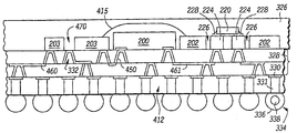
도 7은 입력/출력 전원(201)으로 불리는 기준 전압면으로부터 보다 높은 전압을 수신하도록 전기적으로 접속되고, 코어 전원(203)으로 불리는 기준 전압면으로부터 보다 높은 전압을 수신하기 위해 전기적으로 접속되고, 입력/출력 접지(204)로 불리는 기준 전압면으로부터 보다 낮거나 접지 전압을 수신하기 위해 전기적으로 접속되고, 코어 접지(202)로 불리는 기준 전압면으로부터 보다 낮거나 접지 전압을 수신하도록 전기적으로 접속된 회로 디바이스(200)를 도시한다. 본 발명의 일부 실시예들에서, 입력/출력 전원(201), 코어 전원(203), 입력/출력 접지(204), 및 코어 접지(202)는, 모두 상호 전기적으로 절연된, 전기적 도전층의 부분들이다. 본 발명의 일 실시예에서, 입력/출력 전원(201) 및 입력/출력 접지(204)는 커패시터들(212 및 213)을 분리하는 방식에 의해 전기적으로 분리된다. 유사하게, 코어 전원(203) 및 코어 접지(202)는 커패시터들(214 및 215)을 분리하는 방식에 의해 전기적으로 분리될 수 있다. 설명된 실시예에서, 접점 패드들(216)은 커패시터들(212-215)이 기준 전압면들(201-204)과 전기적으로 접속시키는데 이용됨을 주목한다. 커패시터들(212-215)을 분리하는 것은 예를 들어, 솔더링 또는 도전성 접착과 같은 당 분야에 공지된 다양한 방법들을 이용하여 접점 패드들(216)과 전기적으로 접속될 수 있다.7 is electrically connected to receive a higher voltage from a reference voltage plane called input /
도 7 및 8을 참조하면, 본 발명의 일부 실시예들에서, 회로 디바이스(200)는 상호 접속층(328)의 부분(450)에 의해 전기적 도전층(201-204, 224)의 코어 전원 부분(203)에 전기적으로 접속될 수 있음을 주목한다. 대안적인 실시예들에서, 회로 디바이스(200)는 전기적 도전층(201-204, 224)의 임의의 원하는 부분(예를 들어, 201-204)에 전기적으로 접속될 수 있다. 전기적 도전층(201-204, 224), 또는 이들의 전기적으로 절연된 부분들은 하나 이상의 기준 전압면들로서 기능할 수 있다.7 and 8, in some embodiments of the present invention, the
본 발명의 일부 실시예들에 대해, 캡슐제 층(326)(도 8 참조)은 전기적으로 도전될 수 있다. 캡슐제 층(326)이 전기적으로 도전되면, 하나 이상의 개구들(예를 들어, 개구(470))는 도전층(202, 203, 224)을 통하여 상호 접속층(328)까지 형성될 수 있다. 개구(470)는 도전층(203, 202, 224)의 부분(203)내 개구이다. 개구(470)는 비어(332)에 의해 캡슐제 층(326)과 상호 접속층(328)의 하나 이상의 부분들을 전기적으로 접속하는데 이용될 수 있다. 예를 들어, 캡슐제 층(326)은 개구(470), 비어(332), 및 상호 접속층(328)에 의해 적절한 전압(예를 들어, 전원 또는 접지)을 캡슐제 층(326)에 전기적으로 접속함으로써 기준 전압면으로서 이용될 수 있다. 이 실시예에서, 도전층(202, 203)의 영역 커버리지가 작을지라도, 예를 들어, 도체(460)(도 8 참조)와 같은 제어된 임피던스 회로들이 기준면으로 역할하는 캡슐제 층(326)과 함께 상호 접속층(328)내에 가능하다. 또한, 캡슐제 층(326)은 회로 디바이스(200)용 전기적 차폐 기능(electrically shielding function)을 수행할 수 있다. 캡슐제 층(326)이 전기적 도체이면, 전기적 디바이스(예를 들어, 220)는, 그 단자들이 전기적으로 단락되는 사실로 인해 도 8에 도시된 바와 같이 캡슐제 층(326)내에서 캡슐화되지 않을 것이다.For some embodiments of the invention, the capsule layer 326 (see FIG. 8) may be electrically conductive. Once the capsule layer 326 is electrically conductive, one or more openings (eg, opening 470) may be formed through the
본 발명의 대안적인 실시예들은 전기적 도체인 캡슐제를 이용하지 않을 수 있다. 도 8을 참조하여, 캡슐제 층(326)이 전기적 비도전성이면, 전기적 도전층(415)은 전기적 차폐 및 전압 기준을 제공하기 위해 회로 디바이스(200) 위에 위치하여 형성될 수 있다. 전기적 도전층(415)은 다중-단계 캡슐화 프로세스의 일부로서 형성될 수 있음을 주목한다. 전기적 비-도전 캡슐제 층(326)은 이후의 다중-단계 캡슐화 프로세스의 후속 일부로서 층(415) 위에 위치하여 형성될 수 있다. 본 발명의 대안적인 실시예들에서, 하나 이상의 회로 디바이스(예를 들어, 200)는 단일 전기적 도전층(415)내에 위치될 수 있다.Alternative embodiments of the invention may not use capsules, which are electrical conductors. Referring to FIG. 8, if the capsule layer 326 is electrically nonconductive, an electrically
상호 접속층(328)은 하나 이상의 레벨들의 상호 접속을 포함할 수 있고, 예를 들어, 고밀도 상호 접속 빌드-업(high density interconnect build-up), 적층물(lamination), 또는 박막 프로세싱과 같은 당 분야에서 공지된 다양한 회로화 프로세스들을 이용하여 형성될 수 있다. 본 발명의 일부 실시예들에서, 컴플리언트 폴리머 층(412)을 통과하는 비어(331)는 상호 접속층(328)의 접점 패드(330)를 전기적 도전 볼(334)과 접속시킨다. 본 발명의 대안적인 실시예들은 상호 접속층(328)과 전기적으로 접속하는 복수의 이러한 비어들과 복수의 볼들(예를 들어, 334)을 가질 수 있다. 전기적 도전 볼(334)은 예를 들어, 솔더, 또는 폴리머 코어(338)를 둘러싸는 솔더(336)와 같은 임의의 적절한 도전 물질로 형성될 수 있다. 본 발명의 일부 실시예들에서, 상호 접속층(328)(예를 들어, 412, 331, 330,334)의 아래의 구조는 상호 접속층(328)과, 전기적 도전 볼들(예를 들어, 334)에 그 후에 접착된 부가적인 구조(도시 없음) 사이에 스트레스 버퍼링을 제공하도록 기능할 수 있다.
본 발명의 일부 실시예들에서, 수동 또는 능동 중 하나인 전기 디바이스(220)는 전기적 도전층(224)의 상부 표면에 전기적으로 접속될 수 있으며, 이는 도전층(202)의 절연된 부분 그 자체이다. 전기 디바이스(220)의 좌측 단자에 전기적으로 접속된 좌측 부분(224)은, 전기 디바이스(220)의 우측 단자에 전기적으로 접속된 좌측 부분(224)으로부터 전기적으로 절연될 수 있음을 주목한다. 일 실시예에서, 전기 디바이스(220)는 224의 상부 표면 상에 제작된 하나 이상의 접점 패드들(228)에 의해 전기적 도전층(224)에 전기적으로 접속된다. 따라서, 전기 디바이스(220)는 도전층(224)에 의해 상호 접속층(328)에 전기적으로 접속된다. 본 발명의 일부 실시예들에서, 캡슐제 층(326)의 하나 이상의 부분들(예를 들어, 226)은 도전층(예를 들어, 224)의 하나 이상의 부분들을 절연시키는 역할을 할 수 있다. 디바이스(220)의 전기적 접속은 예를 들어, 솔더링 또는 도전성 접착과 같은 당 분야에 공지된 다양한 방법들을 이용하여 수행될 수 있다. 본 발명의 일부 실시예들에서, 도전층(224)은, 회로 디바이스(220)에 대한 보다 낮은 접착 높이와 패키지에 대한 보다 낮은 포텐셜 프로파일을 허용하는 도전층(202-203)의 잔여 부분들과 비교하여 높이가 감소될 수 있음을 주목한다.In some embodiments of the invention, the
전기적 도전층(202, 203, 224)은 임의의 적절한 전기적 도전 물질로 형성될 수 있다. 본 발명의 일부 실시예들에서, 전기적 도전층(202, 203, 224)은 예를 들어, 리드 프레임과 같은 전기적 도전 프레임일 수 있다. 리드 프레임은 예를 들어 구리 또는 합금(42)과 같은 임의의 전기적 도전 물질로 형성될 수 있다. 본 발명의 대안적인 실시예들에서, 전기적 도전층(202, 203, 224)은 복수의 상호 접속층들을 포함하는, 예를 들어 다중-층 기판과 같은 전기적 도전 기판일 수 있다.The electrically
상호 접속층(328)이 예를 들어, 액정 폴리머(Liquid crystal polymer)(LCP) 또는 폴리페닐렌 황화물(Polyphenylene sulfide))(PPS)과 같이 열가소성 같은, 캡슐제 층(326)과 동일한 카테고리의 물질을 이용하여 형성되면, 회로 디바이스(200) 및 상호 접속층(328)내의 이에 대응하는 상호 접속들은 심리스(seemless)내에 인케이싱(encased)될 수 있고, 도 8에 도시된 캡슐제 층(326)과 상호 접속층(328) 사이의 인터페이스들을 나타내는 수평선들과 물질의 모노리식 블록(monolithic block)은 더 이상 존재하지 않을 것임을 주목한다. 이러한 패키지 구성은, 박막으로 갈라진 비유사 물질들 사이의 인터페이스들의 수가 감소하고 보다 적은 수분 인그레스(less moisture ingress)로 인해 신뢰성이 개선됨을 증명한다. 본 발명의 일 실시예에서, 상호 접속층(328)의 제조를 위한 적층 기술은, 동일한 카테고리의 물질이 캡슐제 층(326)과 상호 접속층(328)을 위해 이용되는 경우에 이용될 수 있다. 또한 주입 몰딩은 이 경우의 캡슐제 층(326)을 도포하는데 이용될 수 있다.The
본 발명의 일부 실시예들에서, 캡슐제 층(126)이 전기적으로 도전되지 않을 때, 전기적 도전층(예를 들어, 도 6의 100; 도 7의 201-204 및 224; 도 8의 224)의 하나 이상의 부분들은 전기 접속들을 다른 디비이스들로 제공하기 위해 (예를 들어, 도 6의 102와 도 8의 220) 물리적으로 분리되거나 그렇지 않으면 전기적 도전층의 다른 부분들로부터 전기적으로 절연될 수 있음을 주목한다.In some embodiments of the invention, when the
앞의 명세서에서, 본 발명은 특정 실시예들을 참조하여 설명되었다. 그러나, 당업자는 아래의 청구 범위에 제시된 본 발명의 범위로부터 벗어남 없이 다양한 수정들과 변경들이 이루어질 수 있음을 이해한다. 따라서, 설명서 및 도면들은 제한적이기 보다는 설명적인 의미로 이해하여야하고, 이러한 모든 수정들이 본 발명의 범위내에 포함됨을 의도한다.In the foregoing specification, the invention has been described with reference to specific embodiments. However, one of ordinary skill in the art appreciates that various modifications and changes can be made without departing from the scope of the present invention as set forth in the claims below. The description and drawings are, accordingly, to be regarded in an illustrative rather than a restrictive sense, and all such modifications are intended to be included within the scope of present invention.
혜택들, 다른 유익함들, 및 문제들에 대한 해결들이 특정 실시예들에 관해 상술되었다. 그러나, 임의의 혜택, 유익함, 또는 발생하거나 더욱 표명되는 해결들을 유발할 수 있는 혜택들, 다른 유익함들, 문제들에 대한 해결들, 및 임의의 요소(들)는 임의의 또는 모든 청구 범위들의 결정적인, 요구된, 필수적 특징 또는 요소로 해석되어서는 않된다. 여기에 이용된 용어들, "포함하다"는 비-배타적인 포함까지 포함하도록 의도하여, 리스트된 요소들을 포함하는 프로세스, 방법, 물품, 또는 장치는 그 요소들만을 포함하는 것은 아니고, 명시적으로 리스트되지 않은 다른 요소들, 또는 이러한 프로세스, 방법, 물품, 또는 장치에 대한 본래의 요소를 포함할 수 있다.
Benefits, other benefits, and solutions to problems have been described above with regard to specific embodiments. However, any benefit, benefit, or benefit that may cause an occurrence or more pronounced solutions, other benefits, solutions to problems, and any element (s) may be attributed to any or all claims. It should not be construed as decisive, required, or essential features or elements. As used herein, the term "comprises" is intended to include non-exclusive inclusions, so that a process, method, article, or apparatus that includes the listed elements does not include only those elements, but explicitly Other elements not listed, or the original elements for such a process, method, article, or apparatus.
9 : 지지 구조 10 : 전기적 도전층
12 : 접착층 14 : 회로 디바이스들
19 : 접점 패드들 24 : 캡슐제 층9: supporting structure 10: electrically conductive layer
12: adhesive layer 14: circuit devices
19
Claims (7)
능동 회로를 포함하는 제 1 표면과 상기 제 1 표면에 대향하는 제 2 표면을 갖는 회로 디바이스;
제 1 표면, 상기 제 1 표면에 대향하는 제 2 표면, 및 적어도 하나의 개구를 갖는 전기적 도전층으로서,
상기 적어도 하나의 개구는 상기 회로 디바이스를 적어도 부분적으로 둘러싸고,
상기 회로 디바이스의 상기 제 1 표면은 상기 전기적 도전층의 상기 제 1 표면과 실질적으로 동일 평면이고,
상기 전기적 도전층은 제 1 기준 전압면을 포함하는, 상기 전기적 도전층;
상기 제 1 기준 전압면에 전기적으로 결합된 전기적 접점(electrical contact)으로서, 전기적 접촉이 상기 제 1 기준 전압면에 형성되도록 하는 상기 전기적 접점; 및
상기 회로 디바이스와 상기 전기적 도전층 사이의 상기 적어도 하나의 개구 내 갭을 적어도 부분적으로 채우는 캡슐제 층(encapsulant layer)으로서, 상기 전기적 도전층은 서로 전기적으로 절연된 적어도 두 부분들을 포함하는 상기 캡슐제 층을 포함하는, 적어도 부분적인 패키징을 갖는 디바이스.In a device with at least partial packaging:
A circuit device having a first surface comprising an active circuit and a second surface opposite the first surface;
An electrically conductive layer having a first surface, a second surface opposite the first surface, and at least one opening,
The at least one opening at least partially surrounds the circuit device,
The first surface of the circuit device is substantially coplanar with the first surface of the electrically conductive layer,
The electrically conductive layer comprises a first reference voltage plane;
An electrical contact electrically coupled to the first reference voltage plane, wherein the electrical contact causes an electrical contact to be formed on the first reference voltage plane; And
An encapsulant layer at least partially filling a gap in the at least one opening between the circuit device and the electrically conductive layer, the electrically conductive layer comprising at least two portions electrically insulated from each other A device having at least partial packaging, comprising a layer.
능동 회로를 포함하는 제 1 표면과 상기 제 1 표면에 대향하는 제 2 표면을 갖는 회로 디바이스;
제 1 표면, 상기 제 1 표면에 대향하는 제 2 표면, 및 적어도 하나의 개구를 갖는 전기적 도전 프레임으로서,
상기 회로 디바이스는 상기 적어도 하나의 개구 내에 있고,
상기 회로 디바이스의 상기 제 1 표면은 상기 전기적 도전 프레임의 상기 제 1 표면과 실질적으로 동일 평면이고,
상기 전기적 도전 프레임은 기준 전압면을 포함하는, 상기 전기적 도전 프레임;
상기 기준 전압면에 전기적으로 결합된 전기적 접점으로서, 전기적 접촉이 상기 기준 전압면에 형성되도록 하는 상기 전기적 접점; 및
상기 회로 디바이스의 상기 제 2 표면과 상기 전기적 도전 프레임의 상기 제 2 표면 위에 놓여진 캡슐제(encapsulant)로서, 전기적 도전 물질을 포함하는 상기 캡슐제를 포함하는, 적어도 부분적인 패키징을 갖는 디바이스.In a device with at least partial packaging:
A circuit device having a first surface comprising an active circuit and a second surface opposite the first surface;
An electrically conductive frame having a first surface, a second surface opposite the first surface, and at least one opening,
The circuit device is in the at least one opening,
The first surface of the circuit device is substantially coplanar with the first surface of the electrically conductive frame,
The electrically conductive frame comprises a reference voltage plane;
An electrical contact electrically coupled to the reference voltage plane, the electrical contact allowing electrical contact to be formed on the reference voltage plane; And
An encapsulant overlying the second surface of the circuit device and the second surface of the electrically conductive frame, the device comprising at least partially packaging comprising an electrically conductive material.
능동 회로를 포함하는 제 1 표면과 상기 제 1 표면에 대향하는 제 2 표면을 갖는 회로 디바이스;
제 1 표면, 상기 제 1 표면에 대향하는 제 2 표면, 및 적어도 하나의 개구를 갖는 전기적 도전층으로서,
상기 적어도 하나의 개구는 상기 회로 디바이스를 적어도 부분적으로 둘러싸고,
상기 회로 디바이스의 상기 제 1 표면은 상기 전기적 도전층의 상기 제 1 표면과 실질적으로 동일 평면이고,
상기 전기적 도전층은 제 1 기준 전압면을 포함하는, 상기 전기적 도전층;
상기 제 1 기준 전압면에 전기적으로 결합된 전기적 접점으로서, 전기적 접촉이 상기 제 1 기준 전압면에 형성되도록 하는 상기 전기적 접점; 및
상기 회로 디바이스와 상기 전기적 도전층 사이의 상기 적어도 하나의 개구 내 갭을 적어도 부분적으로 채우는 캡슐제 층으로서, 상기 전기적 도전층의 상기 제 2 표면의 적어도 제 1 부분 위에 놓여지는 상기 캡슐제 층을 포함하는, 적어도 부분적인 패키징을 갖는 디바이스.In a device with at least partial packaging:
A circuit device having a first surface comprising an active circuit and a second surface opposite the first surface;
An electrically conductive layer having a first surface, a second surface opposite the first surface, and at least one opening,
The at least one opening at least partially surrounds the circuit device,
The first surface of the circuit device is substantially coplanar with the first surface of the electrically conductive layer,
The electrically conductive layer comprises a first reference voltage plane;
An electrical contact electrically coupled to the first reference voltage plane, the electrical contact allowing electrical contact to be formed on the first reference voltage plane; And
A capsule layer at least partially filling the gap in the at least one opening between the circuit device and the electrically conductive layer, the capsule layer overlying at least a first portion of the second surface of the electrically conductive layer Device with at least partial packaging.
능동 회로를 포함하는 제 1 표면과 상기 제 1 표면에 대향하는 제 2 표면을 갖는 회로 디바이스;
제 1 표면, 상기 제 1 표면에 대향하는 제 2 표면, 및 적어도 하나의 개구를 갖는 전기적 도전층으로서,
상기 적어도 하나의 개구는 상기 회로 디바이스를 적어도 부분적으로 둘러싸고,
상기 회로 디바이스의 상기 제 1 표면은 상기 전기적 도전층의 상기 제 1 표면과 실질적으로 동일 평면이고,
상기 전기적 도전층은 제 1 기준 전압면을 포함하는, 상기 전기적 도전층;
상기 제 1 기준 전압면에 전기적으로 결합된 전기적 접점으로서, 전기적 접촉이 상기 제 1 기준 전압면에 형성되도록 하는 상기 전기적 접점; 및
상기 회로 디바이스와 상기 전기적 도전층 사이의 상기 적어도 하나의 개구 내 갭을 적어도 부분적으로 채우는 캡슐제 층으로서, 상기 회로 디바이스의 상기 제 2 표면의 적어도 일부분 위에 놓여지는 상기 캡슐제 층을 포함하는, 적어도 부분적인 패키징을 갖는 디바이스.In a device with at least partial packaging:
A circuit device having a first surface comprising an active circuit and a second surface opposite the first surface;
An electrically conductive layer having a first surface, a second surface opposite the first surface, and at least one opening,
The at least one opening at least partially surrounds the circuit device,
The first surface of the circuit device is substantially coplanar with the first surface of the electrically conductive layer,
The electrically conductive layer comprises a first reference voltage plane;
An electrical contact electrically coupled to the first reference voltage plane, the electrical contact to allow an electrical contact to be formed on the first reference voltage plane; And
A capsule layer at least partially filling the gap in the at least one opening between the circuit device and the electrically conductive layer, the capsule layer overlying at least a portion of the second surface of the circuit device, at least Devices with partial packaging.
능동 회로를 포함하는 제 1 표면과 상기 제 1 표면에 대향하는 제 2 표면을 갖는 회로 디바이스;
제 1 표면, 상기 제 1 표면에 대향하는 제 2 표면, 및 적어도 하나의 개구를 갖는 전기적 도전층으로서,
상기 적어도 하나의 개구는 상기 회로 디바이스를 적어도 부분적으로 둘러싸고,
상기 회로 디바이스의 상기 제 1 표면은 상기 전기적 도전층의 상기 제 1 표면과 실질적으로 동일 평면이고,
상기 전기적 도전층은 제 1 기준 전압면을 포함하는, 상기 전기적 도전층;
상기 제 1 기준 전압면에 전기적으로 결합된 전기적 접점으로서, 전기적 접촉이 상기 제 1 기준 전압면에 형성되도록 하는 상기 전기적 접점;
상기 회로 디바이스와 상기 전기적 도전층 사이의 상기 적어도 하나의 개구 내 갭을 적어도 부분적으로 채우는 캡슐제 층; 및
복수의 회로 디바이스들로서, 상기 회로 디바이스는 상기 복수의 회로 디바이스들 중 첫 번째 것이고, 상기 전기적 도전층은 복수의 개구들을 포함하고, 상기 복수의 개구들 각각은 상기 복수의 회로 디바이스들 중 하나를 적어도 부분적으로 둘러싸는, 상기 복수의 회로 디바이스들을 포함하는, 적어도 부분적인 패키징을 갖는 디바이스.In a device with at least partial packaging:
A circuit device having a first surface comprising an active circuit and a second surface opposite the first surface;
An electrically conductive layer having a first surface, a second surface opposite the first surface, and at least one opening,
The at least one opening at least partially surrounds the circuit device,
The first surface of the circuit device is substantially coplanar with the first surface of the electrically conductive layer,
The electrically conductive layer comprises a first reference voltage plane;
An electrical contact electrically coupled to the first reference voltage plane, the electrical contact allowing electrical contact to be formed on the first reference voltage plane;
A capsule layer at least partially filling a gap in the at least one opening between the circuit device and the electrically conductive layer; And
A plurality of circuit devices, the circuit device being the first of the plurality of circuit devices, the electrically conductive layer comprising a plurality of openings, each of the plurality of openings at least one of the plurality of circuit devices At least partially packaging, comprising a plurality of circuit devices, partially surrounding.
제 1 표면, 상기 제 1 표면에 대향하는 제 2 표면, 및 적어도 하나의 개구를 갖는 전기적 도전층을 제공하는 단계;
접착층을 상기 전기적 도전층에 접착하는 단계;
상기 적어도 하나의 개구 내의 상기 접착층 상에 회로 디바이스를 위치시키는 단계로서, 상기 회로 디바이스의 활성 표면은 상기 전기적 도전층의 상기 제 1 표면과 실질적으로 동일 평면이고, 상기 전기적 도전층은 기준 전압면을 포함하는, 상기 회로 디바이스를 위치시키는 단계;
상기 기준 전압면에 전기적으로 결합된 전기적 접점을 제공하는 단계;
상기 회로 디바이스와 상기 전기적 도전층 사이의 상기 적어도 하나의 개구 내 갭을 적어도 부분적으로 채우기 위해 캡슐제 층을 형성하는 단계; 및
상기 캡슐제 층을 형성한 후, 상기 접착층을 제거하는 단계를 포함하는, 디바이스 형성 방법.A method of forming a device having at least partial packaging:
Providing an electrically conductive layer having a first surface, a second surface opposite the first surface, and at least one opening;
Adhering an adhesive layer to the electrically conductive layer;
Positioning a circuit device on the adhesive layer in the at least one opening, the active surface of the circuit device being substantially coplanar with the first surface of the electrically conductive layer, the electrically conductive layer being a reference voltage plane. Positioning the circuit device;
Providing an electrical contact electrically coupled to the reference voltage plane;
Forming a capsule layer to at least partially fill a gap in the at least one opening between the circuit device and the electrically conductive layer; And
After forming the capsule layer, removing the adhesive layer.
제 1 표면, 상기 제 1 표면에 대향하는 제 2 표면, 및 적어도 하나의 개구를 갖는 전기적 도전층을 제공하는 단계;
접착층을 상기 전기적 도전층에 접착하는 단계;
상기 적어도 하나의 개구 내의 상기 접착층 상에 회로 디바이스를 위치시키는 단계로서, 상기 회로 디바이스의 활성 표면은 상기 전기적 도전층의 상기 제 1 표면과 실질적으로 동일 평면이고, 상기 전기적 도전층은 기준 전압면을 포함하는, 상기 회로 디바이스를 위치시키는 단계;
상기 기준 전압면에 전기적으로 결합된 전기적 접점을 제공하는 단계; 및
상기 회로 디바이스와 상기 전기적 도전층 사이의 상기 적어도 하나의 개구 내 갭을 적어도 부분적으로 채우기 위해 캡슐제 층을 형성하는 단계로서, 상기 회로 디바이스와 상기 전기적 도전층의 상기 제 2 표면 위에 놓여진 몰드 화합물(mold compound)을 형성하는 단계를 포함하는, 상기 캡슐제 층을 형성하는 단계를 포함하는, 디바이스 형성 방법.A method of forming a device having at least partial packaging:
Providing an electrically conductive layer having a first surface, a second surface opposite the first surface, and at least one opening;
Adhering an adhesive layer to the electrically conductive layer;
Positioning a circuit device on the adhesive layer in the at least one opening, the active surface of the circuit device being substantially coplanar with the first surface of the electrically conductive layer, the electrically conductive layer being a reference voltage plane. Positioning the circuit device;
Providing an electrical contact electrically coupled to the reference voltage plane; And
Forming a capsule layer to at least partially fill the gap in the at least one opening between the circuit device and the electrically conductive layer, wherein a mold compound overlying the second surface of the circuit device and the electrically conductive layer ( forming a capsule layer, the method comprising forming a mold compound.
Applications Claiming Priority (3)
| Application Number | Priority Date | Filing Date | Title |
|---|---|---|---|
| US10/418,790 | 2003-04-18 | ||
| US10/418,790 US6921975B2 (en) | 2003-04-18 | 2003-04-18 | Circuit device with at least partial packaging, exposed active surface and a voltage reference plane |
| PCT/US2004/011871 WO2004095514A2 (en) | 2003-04-18 | 2004-04-06 | Circuit device with at least partial packaging and method for forming |
Related Parent Applications (1)
| Application Number | Title | Priority Date | Filing Date |
|---|---|---|---|
| KR1020057019853A Division KR101165580B1 (en) | 2003-04-18 | 2004-04-06 | Circuit device with at least partial packaging and method for forming |
Publications (2)
| Publication Number | Publication Date |
|---|---|
| KR20110043787A KR20110043787A (en) | 2011-04-27 |
| KR101142314B1 true KR101142314B1 (en) | 2012-05-17 |
Family
ID=33159184
Family Applications (3)
| Application Number | Title | Priority Date | Filing Date |
|---|---|---|---|
| KR1020117006445A Expired - Lifetime KR101142314B1 (en) | 2003-04-18 | 2004-04-06 | A device with at least partial packaging and method for forming |
| KR1020057019853A Expired - Lifetime KR101165580B1 (en) | 2003-04-18 | 2004-04-06 | Circuit device with at least partial packaging and method for forming |
| KR1020117006446A Expired - Lifetime KR101215283B1 (en) | 2003-04-18 | 2004-04-06 | A device with at least partial packaging |
Family Applications After (2)
| Application Number | Title | Priority Date | Filing Date |
|---|---|---|---|
| KR1020057019853A Expired - Lifetime KR101165580B1 (en) | 2003-04-18 | 2004-04-06 | Circuit device with at least partial packaging and method for forming |
| KR1020117006446A Expired - Lifetime KR101215283B1 (en) | 2003-04-18 | 2004-04-06 | A device with at least partial packaging |
Country Status (6)
| Country | Link |
|---|---|
| US (3) | US6921975B2 (en) |
| EP (1) | EP1618606A4 (en) |
| JP (1) | JP5042623B2 (en) |
| KR (3) | KR101142314B1 (en) |
| CN (1) | CN100413065C (en) |
| WO (1) | WO2004095514A2 (en) |
Families Citing this family (144)
| Publication number | Priority date | Publication date | Assignee | Title |
|---|---|---|---|---|
| US6930256B1 (en) | 2002-05-01 | 2005-08-16 | Amkor Technology, Inc. | Integrated circuit substrate having laser-embedded conductive patterns and method therefor |
| US7548430B1 (en) | 2002-05-01 | 2009-06-16 | Amkor Technology, Inc. | Buildup dielectric and metallization process and semiconductor package |
| US7633765B1 (en) | 2004-03-23 | 2009-12-15 | Amkor Technology, Inc. | Semiconductor package including a top-surface metal layer for implementing circuit features |
| US9691635B1 (en) | 2002-05-01 | 2017-06-27 | Amkor Technology, Inc. | Buildup dielectric layer having metallization pattern semiconductor package fabrication method |
| US6964881B2 (en) * | 2002-08-27 | 2005-11-15 | Micron Technology, Inc. | Multi-chip wafer level system packages and methods of forming same |
| US7361533B1 (en) | 2002-11-08 | 2008-04-22 | Amkor Technology, Inc. | Stacked embedded leadframe |
| US6905914B1 (en) | 2002-11-08 | 2005-06-14 | Amkor Technology, Inc. | Wafer level package and fabrication method |
| US7723210B2 (en) | 2002-11-08 | 2010-05-25 | Amkor Technology, Inc. | Direct-write wafer level chip scale package |
| JP3940694B2 (en) * | 2003-04-18 | 2007-07-04 | 株式会社東芝 | Semiconductor device and manufacturing method thereof |
| US6921975B2 (en) * | 2003-04-18 | 2005-07-26 | Freescale Semiconductor, Inc. | Circuit device with at least partial packaging, exposed active surface and a voltage reference plane |
| US7112472B2 (en) * | 2003-06-25 | 2006-09-26 | Intel Corporation | Methods of fabricating a composite carbon nanotube thermal interface device |
| US8569142B2 (en) * | 2003-11-28 | 2013-10-29 | Blackberry Limited | Multi-level thin film capacitor on a ceramic substrate and method of manufacturing the same |
| US7005325B2 (en) * | 2004-02-05 | 2006-02-28 | St Assembly Test Services Ltd. | Semiconductor package with passive device integration |
| US11081370B2 (en) | 2004-03-23 | 2021-08-03 | Amkor Technology Singapore Holding Pte. Ltd. | Methods of manufacturing an encapsulated semiconductor device |
| US10811277B2 (en) | 2004-03-23 | 2020-10-20 | Amkor Technology, Inc. | Encapsulated semiconductor package |
| US7245009B2 (en) * | 2005-06-29 | 2007-07-17 | Motorola, Inc. | Hermetic cavity package |
| US20070000595A1 (en) * | 2005-06-29 | 2007-01-04 | Intel Corporation | Adhesive substrate and method for using |
| KR100722597B1 (en) * | 2005-07-04 | 2007-05-28 | 삼성전기주식회사 | Semiconductor package substrate with dummy region with copper pattern |
| DE102005045767B4 (en) * | 2005-09-23 | 2012-03-29 | Infineon Technologies Ag | Method for producing a semiconductor device with plastic housing composition |
| US7572681B1 (en) | 2005-12-08 | 2009-08-11 | Amkor Technology, Inc. | Embedded electronic component package |
| US20070212813A1 (en) * | 2006-03-10 | 2007-09-13 | Fay Owen R | Perforated embedded plane package and method |
| US8829661B2 (en) * | 2006-03-10 | 2014-09-09 | Freescale Semiconductor, Inc. | Warp compensated package and method |
| US7425464B2 (en) * | 2006-03-10 | 2008-09-16 | Freescale Semiconductor, Inc. | Semiconductor device packaging |
| DE102006012738A1 (en) | 2006-03-17 | 2007-09-20 | Infineon Technologies Ag | Benefits of a composite board with semiconductor chips and plastic housing composition as well as methods and molding for the production thereof |
| JP2007266150A (en) * | 2006-03-28 | 2007-10-11 | Fujitsu Ltd | Thermally conductive bonding material, semiconductor package, heat spreader, semiconductor chip, and bonding method for bonding semiconductor chip and heat spreader |
| US7573112B2 (en) * | 2006-04-14 | 2009-08-11 | Allegro Microsystems, Inc. | Methods and apparatus for sensor having capacitor on chip |
| US7687882B2 (en) * | 2006-04-14 | 2010-03-30 | Allegro Microsystems, Inc. | Methods and apparatus for integrated circuit having multiple dies with at least one on chip capacitor |
| US8072059B2 (en) * | 2006-04-19 | 2011-12-06 | Stats Chippac, Ltd. | Semiconductor device and method of forming UBM fixed relative to interconnect structure for alignment of semiconductor die |
| US7993972B2 (en) | 2008-03-04 | 2011-08-09 | Stats Chippac, Ltd. | Wafer level die integration and method therefor |
| JP4791244B2 (en) * | 2006-05-11 | 2011-10-12 | 新光電気工業株式会社 | Electronic component built-in substrate and manufacturing method thereof |
| US7902660B1 (en) | 2006-05-24 | 2011-03-08 | Amkor Technology, Inc. | Substrate for semiconductor device and manufacturing method thereof |
| US7405102B2 (en) * | 2006-06-09 | 2008-07-29 | Freescale Semiconductor, Inc. | Methods and apparatus for thermal management in a multi-layer embedded chip structure |
| US7892882B2 (en) * | 2006-06-09 | 2011-02-22 | Freescale Semiconductor, Inc. | Methods and apparatus for a semiconductor device package with improved thermal performance |
| US20080013298A1 (en) | 2006-07-14 | 2008-01-17 | Nirmal Sharma | Methods and apparatus for passive attachment of components for integrated circuits |
| TWI313943B (en) * | 2006-10-24 | 2009-08-21 | Chipmos Technologies Inc | Light emitting chip package and manufacturing thereof |
| US7550857B1 (en) | 2006-11-16 | 2009-06-23 | Amkor Technology, Inc. | Stacked redistribution layer (RDL) die assembly package |
| US7588951B2 (en) * | 2006-11-17 | 2009-09-15 | Freescale Semiconductor, Inc. | Method of packaging a semiconductor device and a prefabricated connector |
| US7476563B2 (en) | 2006-11-17 | 2009-01-13 | Freescale Semiconductor, Inc. | Method of packaging a device using a dielectric layer |
| US7807511B2 (en) | 2006-11-17 | 2010-10-05 | Freescale Semiconductor, Inc. | Method of packaging a device having a multi-contact elastomer connector contact area and device thereof |
| US7696016B2 (en) * | 2006-11-17 | 2010-04-13 | Freescale Semiconductor, Inc. | Method of packaging a device having a tangible element and device thereof |
| US7674656B2 (en) * | 2006-12-06 | 2010-03-09 | Freescale Semiconductor, Inc. | Die positioning for packaged integrated circuits |
| US20080246126A1 (en) * | 2007-04-04 | 2008-10-09 | Freescale Semiconductor, Inc. | Stacked and shielded die packages with interconnects |
| US8106496B2 (en) * | 2007-06-04 | 2012-01-31 | Stats Chippac, Inc. | Semiconductor packaging system with stacking and method of manufacturing thereof |
| US7648858B2 (en) * | 2007-06-19 | 2010-01-19 | Freescale Semiconductor, Inc. | Methods and apparatus for EMI shielding in multi-chip modules |
| US8217511B2 (en) * | 2007-07-31 | 2012-07-10 | Freescale Semiconductor, Inc. | Redistributed chip packaging with thermal contact to device backside |
| US7838420B2 (en) * | 2007-08-29 | 2010-11-23 | Freescale Semiconductor, Inc. | Method for forming a packaged semiconductor device |
| US7679177B2 (en) * | 2007-09-21 | 2010-03-16 | Stats Chippac Ltd. | Integrated circuit packaging system with passive components |
| TWI360207B (en) | 2007-10-22 | 2012-03-11 | Advanced Semiconductor Eng | Chip package structure and method of manufacturing |
| US10074553B2 (en) * | 2007-12-03 | 2018-09-11 | STATS ChipPAC Pte. Ltd. | Wafer level package integration and method |
| US9460951B2 (en) | 2007-12-03 | 2016-10-04 | STATS ChipPAC Pte. Ltd. | Semiconductor device and method of wafer level package integration |
| US7759212B2 (en) * | 2007-12-26 | 2010-07-20 | Stats Chippac, Ltd. | System-in-package having integrated passive devices and method therefor |
| US20090170241A1 (en) * | 2007-12-26 | 2009-07-02 | Stats Chippac, Ltd. | Semiconductor Device and Method of Forming the Device Using Sacrificial Carrier |
| US7741194B2 (en) * | 2008-01-04 | 2010-06-22 | Freescale Semiconductor, Inc. | Removable layer manufacturing method |
| US7950144B2 (en) * | 2008-04-30 | 2011-05-31 | Freescale Semiconductor, Inc. | Method for controlling warpage in redistributed chip packaging panels |
| US8032030B2 (en) * | 2008-05-30 | 2011-10-04 | Freescale Semiconductor, Inc. | Multiple core system |
| US8294483B2 (en) * | 2008-05-30 | 2012-10-23 | Freescale Semiconductor, Inc. | Testing of multiple integrated circuits |
| US8093704B2 (en) * | 2008-06-03 | 2012-01-10 | Intel Corporation | Package on package using a bump-less build up layer (BBUL) package |
| US8093670B2 (en) | 2008-07-24 | 2012-01-10 | Allegro Microsystems, Inc. | Methods and apparatus for integrated circuit having on chip capacitor with eddy current reductions |
| US8236609B2 (en) * | 2008-08-01 | 2012-08-07 | Freescale Semiconductor, Inc. | Packaging an integrated circuit die with backside metallization |
| US20100052424A1 (en) * | 2008-08-26 | 2010-03-04 | Taylor William P | Methods and apparatus for integrated circuit having integrated energy storage device |
| US7763976B2 (en) * | 2008-09-30 | 2010-07-27 | Freescale Semiconductor, Inc. | Integrated circuit module with integrated passive device |
| US7935571B2 (en) * | 2008-11-25 | 2011-05-03 | Freescale Semiconductor, Inc. | Through substrate vias for back-side interconnections on very thin semiconductor wafers |
| US8344503B2 (en) | 2008-11-25 | 2013-01-01 | Freescale Semiconductor, Inc. | 3-D circuits with integrated passive devices |
| US7960827B1 (en) | 2009-04-09 | 2011-06-14 | Amkor Technology, Inc. | Thermal via heat spreader package and method |
| US8623753B1 (en) | 2009-05-28 | 2014-01-07 | Amkor Technology, Inc. | Stackable protruding via package and method |
| US8222538B1 (en) | 2009-06-12 | 2012-07-17 | Amkor Technology, Inc. | Stackable via package and method |
| TWI456715B (en) * | 2009-06-19 | 2014-10-11 | 日月光半導體製造股份有限公司 | Chip package structure and method of manufacturing same |
| TWI466259B (en) * | 2009-07-21 | 2014-12-21 | 日月光半導體製造股份有限公司 | Semiconductor package, method of manufacturing the same, and method of manufacturing a re-wipe wafer encapsulant |
| TWI405306B (en) * | 2009-07-23 | 2013-08-11 | 日月光半導體製造股份有限公司 | Semiconductor package, method of manufacturing the same, and repeating wafer encapsulant |
| US8471154B1 (en) | 2009-08-06 | 2013-06-25 | Amkor Technology, Inc. | Stackable variable height via package and method |
| US8796561B1 (en) | 2009-10-05 | 2014-08-05 | Amkor Technology, Inc. | Fan out build up substrate stackable package and method |
| US20110084372A1 (en) | 2009-10-14 | 2011-04-14 | Advanced Semiconductor Engineering, Inc. | Package carrier, semiconductor package, and process for fabricating same |
| US8148206B2 (en) * | 2009-10-27 | 2012-04-03 | Freescale Semiconductor, Inc. | Package for high power integrated circuits and method for forming |
| US8378466B2 (en) | 2009-11-19 | 2013-02-19 | Advanced Semiconductor Engineering, Inc. | Wafer-level semiconductor device packages with electromagnetic interference shielding |
| TWI497679B (en) * | 2009-11-27 | 2015-08-21 | 日月光半導體製造股份有限公司 | Semiconductor package and method of manufacturing same |
| US8937381B1 (en) | 2009-12-03 | 2015-01-20 | Amkor Technology, Inc. | Thin stackable package and method |
| US20110133732A1 (en) * | 2009-12-03 | 2011-06-09 | Allegro Microsystems, Inc. | Methods and apparatus for enhanced frequency response of magnetic sensors |
| US9691734B1 (en) | 2009-12-07 | 2017-06-27 | Amkor Technology, Inc. | Method of forming a plurality of electronic component packages |
| US8569894B2 (en) | 2010-01-13 | 2013-10-29 | Advanced Semiconductor Engineering, Inc. | Semiconductor package with single sided substrate design and manufacturing methods thereof |
| US8372689B2 (en) * | 2010-01-21 | 2013-02-12 | Advanced Semiconductor Engineering, Inc. | Wafer-level semiconductor device packages with three-dimensional fan-out and manufacturing methods thereof |
| US8536462B1 (en) | 2010-01-22 | 2013-09-17 | Amkor Technology, Inc. | Flex circuit package and method |
| US8320134B2 (en) | 2010-02-05 | 2012-11-27 | Advanced Semiconductor Engineering, Inc. | Embedded component substrate and manufacturing methods thereof |
| TWI411075B (en) | 2010-03-22 | 2013-10-01 | 日月光半導體製造股份有限公司 | Semiconductor package and method of manufacturing same |
| US8624374B2 (en) | 2010-04-02 | 2014-01-07 | Advanced Semiconductor Engineering, Inc. | Semiconductor device packages with fan-out and with connecting elements for stacking and manufacturing methods thereof |
| US8278746B2 (en) | 2010-04-02 | 2012-10-02 | Advanced Semiconductor Engineering, Inc. | Semiconductor device packages including connecting elements |
| US8324511B1 (en) | 2010-04-06 | 2012-12-04 | Amkor Technology, Inc. | Through via nub reveal method and structure |
| US8866301B2 (en) * | 2010-05-18 | 2014-10-21 | Taiwan Semiconductor Manufacturing Company, Ltd. | Package systems having interposers with interconnection structures |
| US8300423B1 (en) | 2010-05-25 | 2012-10-30 | Amkor Technology, Inc. | Stackable treated via package and method |
| US8294276B1 (en) | 2010-05-27 | 2012-10-23 | Amkor Technology, Inc. | Semiconductor device and fabricating method thereof |
| US8216918B2 (en) | 2010-07-23 | 2012-07-10 | Freescale Semiconductor, Inc. | Method of forming a packaged semiconductor device |
| US8338229B1 (en) | 2010-07-30 | 2012-12-25 | Amkor Technology, Inc. | Stackable plasma cleaned via package and method |
| US8440554B1 (en) | 2010-08-02 | 2013-05-14 | Amkor Technology, Inc. | Through via connected backside embedded circuit features structure and method |
| US8717775B1 (en) | 2010-08-02 | 2014-05-06 | Amkor Technology, Inc. | Fingerprint sensor package and method |
| US8598709B2 (en) * | 2010-08-31 | 2013-12-03 | Infineon Technologies Ag | Method and system for routing electrical connections of semiconductor chips |
| US8461698B1 (en) * | 2010-09-28 | 2013-06-11 | Rockwell Collins, Inc. | PCB external ground plane via conductive coating |
| US8487445B1 (en) | 2010-10-05 | 2013-07-16 | Amkor Technology, Inc. | Semiconductor device having through electrodes protruding from dielectric layer |
| US8337657B1 (en) | 2010-10-27 | 2012-12-25 | Amkor Technology, Inc. | Mechanical tape separation package and method |
| US8482134B1 (en) | 2010-11-01 | 2013-07-09 | Amkor Technology, Inc. | Stackable package and method |
| TWI455265B (en) * | 2010-11-01 | 2014-10-01 | 矽品精密工業股份有限公司 | Package structure with MEMS components and its manufacturing method |
| US9748154B1 (en) | 2010-11-04 | 2017-08-29 | Amkor Technology, Inc. | Wafer level fan out semiconductor device and manufacturing method thereof |
| US8525318B1 (en) | 2010-11-10 | 2013-09-03 | Amkor Technology, Inc. | Semiconductor device and fabricating method thereof |
| US8941222B2 (en) | 2010-11-11 | 2015-01-27 | Advanced Semiconductor Engineering Inc. | Wafer level semiconductor package and manufacturing methods thereof |
| US8557629B1 (en) | 2010-12-03 | 2013-10-15 | Amkor Technology, Inc. | Semiconductor device having overlapped via apertures |
| US8791501B1 (en) | 2010-12-03 | 2014-07-29 | Amkor Technology, Inc. | Integrated passive device structure and method |
| US8535961B1 (en) | 2010-12-09 | 2013-09-17 | Amkor Technology, Inc. | Light emitting diode (LED) package and method |
| US9406658B2 (en) | 2010-12-17 | 2016-08-02 | Advanced Semiconductor Engineering, Inc. | Embedded component device and manufacturing methods thereof |
| US8390130B1 (en) | 2011-01-06 | 2013-03-05 | Amkor Technology, Inc. | Through via recessed reveal structure and method |
| US9721872B1 (en) | 2011-02-18 | 2017-08-01 | Amkor Technology, Inc. | Methods and structures for increasing the allowable die size in TMV packages |
| US9013011B1 (en) | 2011-03-11 | 2015-04-21 | Amkor Technology, Inc. | Stacked and staggered die MEMS package and method |
| KR101140113B1 (en) | 2011-04-26 | 2012-04-30 | 앰코 테크놀로지 코리아 주식회사 | Semiconductor device |
| US8653674B1 (en) | 2011-09-15 | 2014-02-18 | Amkor Technology, Inc. | Electronic component package fabrication method and structure |
| US8633598B1 (en) | 2011-09-20 | 2014-01-21 | Amkor Technology, Inc. | Underfill contacting stacking balls package fabrication method and structure |
| US9029962B1 (en) | 2011-10-12 | 2015-05-12 | Amkor Technology, Inc. | Molded cavity substrate MEMS package fabrication method and structure |
| US8552548B1 (en) | 2011-11-29 | 2013-10-08 | Amkor Technology, Inc. | Conductive pad on protruding through electrode semiconductor device |
| US20130154091A1 (en) * | 2011-12-14 | 2013-06-20 | Jason R. Wright | Semiconductor device packaging using encapsulated conductive balls for package-on-package back side coupling |
| US8629539B2 (en) | 2012-01-16 | 2014-01-14 | Allegro Microsystems, Llc | Methods and apparatus for magnetic sensor having non-conductive die paddle |
| TWI446501B (en) * | 2012-01-20 | 2014-07-21 | 矽品精密工業股份有限公司 | Carrier board, semiconductor package and method of manufacturing same |
| US9812588B2 (en) | 2012-03-20 | 2017-11-07 | Allegro Microsystems, Llc | Magnetic field sensor integrated circuit with integral ferromagnetic material |
| US9494660B2 (en) | 2012-03-20 | 2016-11-15 | Allegro Microsystems, Llc | Integrated circuit package having a split lead frame |
| US10234513B2 (en) | 2012-03-20 | 2019-03-19 | Allegro Microsystems, Llc | Magnetic field sensor integrated circuit with integral ferromagnetic material |
| US9666788B2 (en) | 2012-03-20 | 2017-05-30 | Allegro Microsystems, Llc | Integrated circuit package having a split lead frame |
| US9048298B1 (en) | 2012-03-29 | 2015-06-02 | Amkor Technology, Inc. | Backside warpage control structure and fabrication method |
| US8916419B2 (en) | 2012-03-29 | 2014-12-23 | Taiwan Semiconductor Manufacturing Company, Ltd. | Lid attach process and apparatus for fabrication of semiconductor packages |
| US9129943B1 (en) | 2012-03-29 | 2015-09-08 | Amkor Technology, Inc. | Embedded component package and fabrication method |
| US9040355B2 (en) | 2012-07-11 | 2015-05-26 | Freescale Semiconductor, Inc. | Sensor package and method of forming same |
| KR101429344B1 (en) | 2012-08-08 | 2014-08-12 | 앰코 테크놀로지 코리아 주식회사 | Semiconductor Package and Manufacturing Methode thereof |
| US8709868B2 (en) | 2012-08-23 | 2014-04-29 | Freescale Semiconductor, Inc. | Sensor packages and method of packaging dies of differing sizes |
| US8659167B1 (en) | 2012-08-29 | 2014-02-25 | Freescale Semiconductor, Inc. | Sensor packaging method and sensor packages |
| KR20140038116A (en) | 2012-09-20 | 2014-03-28 | 제이앤제이 패밀리 주식회사 | Led lamp |
| KR101366461B1 (en) | 2012-11-20 | 2014-02-26 | 앰코 테크놀로지 코리아 주식회사 | Semiconductor device and manufacturing method thereof |
| US9799592B2 (en) | 2013-11-19 | 2017-10-24 | Amkor Technology, Inc. | Semicondutor device with through-silicon via-less deep wells |
| US9704780B2 (en) | 2012-12-11 | 2017-07-11 | STATS ChipPAC, Pte. Ltd. | Semiconductor device and method of forming low profile fan-out package with vertical interconnection units |
| US9258878B2 (en) * | 2013-02-13 | 2016-02-09 | Gerald Ho Kim | Isolation of thermal ground for multiple heat-generating devices on a substrate |
| US8963318B2 (en) * | 2013-02-28 | 2015-02-24 | Freescale Semiconductor, Inc. | Packaged semiconductor device |
| KR101488590B1 (en) | 2013-03-29 | 2015-01-30 | 앰코 테크놀로지 코리아 주식회사 | Semiconductor device and manufacturing method thereof |
| US9411025B2 (en) | 2013-04-26 | 2016-08-09 | Allegro Microsystems, Llc | Integrated circuit package having a split lead frame and a magnet |
| US10418298B2 (en) | 2013-09-24 | 2019-09-17 | STATS ChipPAC Pte. Ltd. | Semiconductor device and method of forming dual fan-out semiconductor package |
| KR101607981B1 (en) | 2013-11-04 | 2016-03-31 | 앰코 테크놀로지 코리아 주식회사 | Interposer and method for manufacturing the same, and semiconductor package using the same |
| KR20170104496A (en) | 2015-01-28 | 2017-09-15 | 콘티넨탈 테베스 아게 운트 코. 오하게 | Sensors with symmetrically buried sensor elements |
| CN107209034B (en) | 2015-01-28 | 2020-03-24 | 大陆-特韦斯股份有限公司 | Adapter with embedded filter part for sensor |
| US10411498B2 (en) | 2015-10-21 | 2019-09-10 | Allegro Microsystems, Llc | Apparatus and methods for extending sensor integrated circuit operation through a power disturbance |
| US9960328B2 (en) | 2016-09-06 | 2018-05-01 | Amkor Technology, Inc. | Semiconductor device and manufacturing method thereof |
| US10978897B2 (en) | 2018-04-02 | 2021-04-13 | Allegro Microsystems, Llc | Systems and methods for suppressing undesirable voltage supply artifacts |
| US10991644B2 (en) | 2019-08-22 | 2021-04-27 | Allegro Microsystems, Llc | Integrated circuit package having a low profile |
Citations (4)
| Publication number | Priority date | Publication date | Assignee | Title |
|---|---|---|---|---|
| KR19990029348A (en) * | 1997-09-08 | 1999-04-26 | 모기 쥰이찌 | Semiconductor devices |
| JPH11312756A (en) * | 1998-04-28 | 1999-11-09 | Nec Corp | Semiconductor device |
| JP2001189411A (en) * | 2000-01-05 | 2001-07-10 | Matsushita Electronics Industry Corp | Method for manufacturing resin-encapsulated semiconductor device |
| WO2002021595A2 (en) * | 2000-09-08 | 2002-03-14 | Intel Corporation | Integrated core microelectronic package |
Family Cites Families (52)
| Publication number | Priority date | Publication date | Assignee | Title |
|---|---|---|---|---|
| US4246595A (en) | 1977-03-08 | 1981-01-20 | Matsushita Electric Industrial Co., Ltd. | Electronics circuit device and method of making the same |
| US4630096A (en) | 1984-05-30 | 1986-12-16 | Motorola, Inc. | High density IC module assembly |
| US4722914A (en) | 1984-05-30 | 1988-02-02 | Motorola Inc. | Method of making a high density IC module assembly |
| US4783695A (en) | 1986-09-26 | 1988-11-08 | General Electric Company | Multichip integrated circuit packaging configuration and method |
| US4835704A (en) * | 1986-12-29 | 1989-05-30 | General Electric Company | Adaptive lithography system to provide high density interconnect |
| US4890156A (en) | 1987-03-13 | 1989-12-26 | Motorola Inc. | Multichip IC module having coplanar dice and substrate |
| US4792533A (en) | 1987-03-13 | 1988-12-20 | Motorola Inc. | Coplanar die to substrate bond method |
| US4882200A (en) * | 1987-05-21 | 1989-11-21 | General Electric Company | Method for photopatterning metallization via UV-laser ablation of the activator |
| US5643472A (en) * | 1988-07-08 | 1997-07-01 | Cauldron Limited Partnership | Selective removal of material by irradiation |
| US5057903A (en) * | 1989-07-17 | 1991-10-15 | Microelectronics And Computer Technology Corporation | Thermal heat sink encapsulated integrated circuit |
| JPH03125443A (en) * | 1989-10-09 | 1991-05-28 | Sharp Corp | Electrode of mounting board and liquid crystal display having the electrode of this mounting board |
| US5169678A (en) * | 1989-12-26 | 1992-12-08 | General Electric Company | Laser ablatable polymer dielectrics and methods |
| US5161093A (en) | 1990-07-02 | 1992-11-03 | General Electric Company | Multiple lamination high density interconnect process and structure employing a variable crosslinking adhesive |
| EP0547807A3 (en) | 1991-12-16 | 1993-09-22 | General Electric Company | Packaged electronic system |
| US5331205A (en) * | 1992-02-21 | 1994-07-19 | Motorola, Inc. | Molded plastic package with wire protection |
| US5310702A (en) * | 1992-03-20 | 1994-05-10 | Kulicke And Soffa Industries, Inc. | Method of preventing short-circuiting of bonding wires |
| US5592025A (en) | 1992-08-06 | 1997-01-07 | Motorola, Inc. | Pad array semiconductor device |
| US5353498A (en) | 1993-02-08 | 1994-10-11 | General Electric Company | Method for fabricating an integrated circuit module |
| US5578869A (en) * | 1994-03-29 | 1996-11-26 | Olin Corporation | Components for housing an integrated circuit device |
| US5604376A (en) * | 1994-06-30 | 1997-02-18 | Digital Equipment Corporation | Paddleless molded plastic semiconductor chip package |
| JPH0873832A (en) * | 1994-09-05 | 1996-03-19 | Hitachi Chem Co Ltd | Resin paste and semiconductor device |
| US5525834A (en) * | 1994-10-17 | 1996-06-11 | W. L. Gore & Associates, Inc. | Integrated circuit package |
| US5616958A (en) * | 1995-01-25 | 1997-04-01 | International Business Machines Corporation | Electronic package |
| JPH11507834A (en) | 1995-06-23 | 1999-07-13 | マイクロメット ゲゼルシャフト ヒュール ビオメディツィニッシェ フォルシュンク エムベーハー | Immortalized epithelial tumor cells |
| US5866952A (en) | 1995-11-30 | 1999-02-02 | Lockheed Martin Corporation | High density interconnected circuit module with a compliant layer as part of a stress-reducing molded substrate |
| US5841193A (en) | 1996-05-20 | 1998-11-24 | Epic Technologies, Inc. | Single chip modules, repairable multichip modules, and methods of fabrication thereof |
| JP3500016B2 (en) * | 1996-09-27 | 2004-02-23 | 三洋電機株式会社 | Semiconductor device and manufacturing method thereof |
| US5989935A (en) | 1996-11-19 | 1999-11-23 | Texas Instruments Incorporated | Column grid array for semiconductor packaging and method |
| US5990545A (en) * | 1996-12-02 | 1999-11-23 | 3M Innovative Properties Company | Chip scale ball grid array for integrated circuit package |
| US6249046B1 (en) * | 1997-02-13 | 2001-06-19 | Seiko Epson Corporation | Semiconductor device and method for manufacturing and mounting thereof, and circuit board mounted with the semiconductor device |
| US6114763A (en) * | 1997-05-30 | 2000-09-05 | Tessera, Inc. | Semiconductor package with translator for connection to an external substrate |
| US5835355A (en) * | 1997-09-22 | 1998-11-10 | Lsi Logic Corporation | Tape ball grid array package with perforated metal stiffener |
| JP3563577B2 (en) * | 1997-10-31 | 2004-09-08 | 京セラ株式会社 | Electronic component surface mounting substrate |
| TW417220B (en) | 1999-07-23 | 2001-01-01 | Advanced Semiconductor Eng | Packaging structure and method of semiconductor chip |
| US6573123B2 (en) * | 1999-09-07 | 2003-06-03 | Sai Man Li | Semiconductor chip package and manufacturing method thereof |
| JP2001177005A (en) * | 1999-12-17 | 2001-06-29 | Fujitsu Ltd | Semiconductor device and manufacturing method thereof |
| US6396148B1 (en) * | 2000-02-10 | 2002-05-28 | Epic Technologies, Inc. | Electroless metal connection structures and methods |
| JP3798220B2 (en) * | 2000-04-07 | 2006-07-19 | シャープ株式会社 | Semiconductor device and liquid crystal module using the same |
| EP1160861B1 (en) * | 2000-06-01 | 2008-01-16 | Matsushita Electric Industrial Co., Ltd. | Method of manufacturing a thermally conductive substrate with leadframe and heat radiation plate |
| US6576494B1 (en) * | 2000-06-28 | 2003-06-10 | Micron Technology, Inc. | Recessed encapsulated microelectronic devices and methods for formation |
| US20020064931A1 (en) | 2000-07-03 | 2002-05-30 | E. C. Ong | Method and apparatus for applying a protective over-coating to a ball-grid-array (BGA) structure |
| US6734534B1 (en) | 2000-08-16 | 2004-05-11 | Intel Corporation | Microelectronic substrate with integrated devices |
| JP2002076040A (en) * | 2000-08-30 | 2002-03-15 | Hitachi Ltd | Semiconductor device and manufacturing method thereof |
| TW473962B (en) | 2001-01-20 | 2002-01-21 | Siliconware Precision Industries Co Ltd | Cavity down ball grid array package and its manufacturing process |
| JP2002280491A (en) * | 2001-03-22 | 2002-09-27 | Matsushita Electric Ind Co Ltd | Electronic component and manufacturing method thereof |
| JP2002314029A (en) * | 2001-04-09 | 2002-10-25 | Taiyo Yuden Co Ltd | Module electronic components |
| JP3983120B2 (en) * | 2001-07-30 | 2007-09-26 | 富士通日立プラズマディスプレイ株式会社 | IC chip mounting structure and display device |
| JP2003068932A (en) * | 2001-08-27 | 2003-03-07 | Kyocera Corp | Wiring board |
| JP2003249604A (en) * | 2002-02-25 | 2003-09-05 | Kato Denki Seisakusho:Kk | Resin-sealed semiconductor device and manufacturing method thereof, lead frame used for resin-sealed semiconductor device, and semiconductor module device |
| JP3801121B2 (en) * | 2002-08-30 | 2006-07-26 | 松下電器産業株式会社 | Resin-sealed semiconductor device and manufacturing method thereof |
| US6921975B2 (en) * | 2003-04-18 | 2005-07-26 | Freescale Semiconductor, Inc. | Circuit device with at least partial packaging, exposed active surface and a voltage reference plane |
| US6838776B2 (en) * | 2003-04-18 | 2005-01-04 | Freescale Semiconductor, Inc. | Circuit device with at least partial packaging and method for forming |
-
2003
- 2003-04-18 US US10/418,790 patent/US6921975B2/en not_active Expired - Lifetime
-
2004
- 2004-04-06 EP EP04759949A patent/EP1618606A4/en not_active Withdrawn
- 2004-04-06 KR KR1020117006445A patent/KR101142314B1/en not_active Expired - Lifetime
- 2004-04-06 CN CNB200480010401XA patent/CN100413065C/en not_active Expired - Lifetime
- 2004-04-06 WO PCT/US2004/011871 patent/WO2004095514A2/en not_active Ceased
- 2004-04-06 KR KR1020057019853A patent/KR101165580B1/en not_active Expired - Lifetime
- 2004-04-06 KR KR1020117006446A patent/KR101215283B1/en not_active Expired - Lifetime
- 2004-04-06 JP JP2006513085A patent/JP5042623B2/en not_active Expired - Lifetime
-
2005
- 2005-07-19 US US11/148,691 patent/US7361987B2/en not_active Expired - Lifetime
-
2008
- 2008-02-28 US US12/039,434 patent/US8072062B2/en not_active Expired - Fee Related
Patent Citations (4)
| Publication number | Priority date | Publication date | Assignee | Title |
|---|---|---|---|---|
| KR19990029348A (en) * | 1997-09-08 | 1999-04-26 | 모기 쥰이찌 | Semiconductor devices |
| JPH11312756A (en) * | 1998-04-28 | 1999-11-09 | Nec Corp | Semiconductor device |
| JP2001189411A (en) * | 2000-01-05 | 2001-07-10 | Matsushita Electronics Industry Corp | Method for manufacturing resin-encapsulated semiconductor device |
| WO2002021595A2 (en) * | 2000-09-08 | 2002-03-14 | Intel Corporation | Integrated core microelectronic package |
Also Published As
| Publication number | Publication date |
|---|---|
| CN100413065C (en) | 2008-08-20 |
| EP1618606A2 (en) | 2006-01-25 |
| CN1774802A (en) | 2006-05-17 |
| JP2006523964A (en) | 2006-10-19 |
| EP1618606A4 (en) | 2011-07-27 |
| KR20050123169A (en) | 2005-12-29 |
| WO2004095514A2 (en) | 2004-11-04 |
| US20080142960A1 (en) | 2008-06-19 |
| US20060012036A1 (en) | 2006-01-19 |
| US6921975B2 (en) | 2005-07-26 |
| WO2004095514A3 (en) | 2005-08-18 |
| US8072062B2 (en) | 2011-12-06 |
| US7361987B2 (en) | 2008-04-22 |
| KR20110043788A (en) | 2011-04-27 |
| US20040207077A1 (en) | 2004-10-21 |
| JP5042623B2 (en) | 2012-10-03 |
| KR20110043787A (en) | 2011-04-27 |
| KR101215283B1 (en) | 2012-12-26 |
| KR101165580B1 (en) | 2012-07-23 |
Similar Documents
| Publication | Publication Date | Title |
|---|---|---|
| KR101142314B1 (en) | A device with at least partial packaging and method for forming | |
| US6838776B2 (en) | Circuit device with at least partial packaging and method for forming | |
| US10276553B2 (en) | Chip package structure and manufacturing method thereof | |
| US6153928A (en) | Substrate for semiconductor package, fabrication method thereof, and stacked-type semiconductor package using the substrate | |
| KR101749284B1 (en) | Integrated circuit packaging system with package stacking and method of manufacture thereof | |
| US6916682B2 (en) | Semiconductor package device for use with multiple integrated circuits in a stacked configuration and method of formation and testing | |
| US20030230801A1 (en) | Semiconductor device assemblies and packages including multiple semiconductor devices and methods | |
| KR101377176B1 (en) | Panel based lead frame packaging method and device | |
| TWI520240B (en) | Ball grid array package for leads on power type wafers | |
| CN102842557B (en) | A packaging structure and manufacturing method thereof | |
| US8963318B2 (en) | Packaged semiconductor device | |
| JPH11251355A (en) | Wire bonded package method and apparatus for integrated circuits | |
| WO2010105157A2 (en) | Microelectronic assembly with impedance controlled wirebond and conductive reference element | |
| CN103579188A (en) | Embedded integrated circuit package and method for manufacturing an embedded integrated circuit package | |
| US20070066139A1 (en) | Electronic plug unit | |
| TW201639426A (en) | Single layered galvanic isolator assembly | |
| US6903441B2 (en) | Semiconductor package with enhanced chip groundability and method of fabricating the same | |
| TWI400773B (en) | Circuit device having at least partially packaged and method of forming same | |
| KR20050074251A (en) | Multi-chip package and semiconductor chip for the same | |
| CN120914118A (en) | Substrate interconnection packaging method and substrate interconnection packaging structure | |
| HK1218182A1 (en) | Heat isolation structures for high bandwidth interconnects |
Legal Events
| Date | Code | Title | Description |
|---|---|---|---|
| A107 | Divisional application of patent | ||
| PA0104 | Divisional application for international application |
St.27 status event code: A-0-1-A10-A18-div-PA0104 St.27 status event code: A-0-1-A10-A16-div-PA0104 |
|
| A201 | Request for examination | ||
| PA0201 | Request for examination |
St.27 status event code: A-1-2-D10-D11-exm-PA0201 |
|
| PG1501 | Laying open of application |
St.27 status event code: A-1-1-Q10-Q12-nap-PG1501 |
|
| E902 | Notification of reason for refusal | ||
| PE0902 | Notice of grounds for rejection |
St.27 status event code: A-1-2-D10-D21-exm-PE0902 |
|
| P11-X000 | Amendment of application requested |
St.27 status event code: A-2-2-P10-P11-nap-X000 |
|
| P13-X000 | Application amended |
St.27 status event code: A-2-2-P10-P13-nap-X000 |
|
| E701 | Decision to grant or registration of patent right | ||
| PE0701 | Decision of registration |
St.27 status event code: A-1-2-D10-D22-exm-PE0701 |
|
| GRNT | Written decision to grant | ||
| PR0701 | Registration of establishment |
St.27 status event code: A-2-4-F10-F11-exm-PR0701 |
|
| PR1002 | Payment of registration fee |
St.27 status event code: A-2-2-U10-U12-oth-PR1002 Fee payment year number: 1 |
|
| R18-X000 | Changes to party contact information recorded |
St.27 status event code: A-5-5-R10-R18-oth-X000 |
|
| PG1601 | Publication of registration |
St.27 status event code: A-4-4-Q10-Q13-nap-PG1601 |
|
| PR1001 | Payment of annual fee |
St.27 status event code: A-4-4-U10-U11-oth-PR1001 Fee payment year number: 4 |
|
| FPAY | Annual fee payment |
Payment date: 20160411 Year of fee payment: 5 |
|
| PR1001 | Payment of annual fee |
St.27 status event code: A-4-4-U10-U11-oth-PR1001 Fee payment year number: 5 |
|
| PR1001 | Payment of annual fee |
St.27 status event code: A-4-4-U10-U11-oth-PR1001 Fee payment year number: 6 |
|
| PN2301 | Change of applicant |
St.27 status event code: A-5-5-R10-R13-asn-PN2301 St.27 status event code: A-5-5-R10-R11-asn-PN2301 |
|
| PR1001 | Payment of annual fee |
St.27 status event code: A-4-4-U10-U11-oth-PR1001 Fee payment year number: 7 |
|
| FPAY | Annual fee payment |
Payment date: 20190401 Year of fee payment: 8 |
|
| PR1001 | Payment of annual fee |
St.27 status event code: A-4-4-U10-U11-oth-PR1001 Fee payment year number: 8 |
|
| PR1001 | Payment of annual fee |
St.27 status event code: A-4-4-U10-U11-oth-PR1001 Fee payment year number: 9 |
|
| PR1001 | Payment of annual fee |
St.27 status event code: A-4-4-U10-U11-oth-PR1001 Fee payment year number: 10 |
|
| PR1001 | Payment of annual fee |
St.27 status event code: A-4-4-U10-U11-oth-PR1001 Fee payment year number: 11 |
|
| PR1001 | Payment of annual fee |
St.27 status event code: A-4-4-U10-U11-oth-PR1001 Fee payment year number: 12 |
|
| PC1801 | Expiration of term |
St.27 status event code: N-4-6-H10-H14-oth-PC1801 Not in force date: 20240407 Ip right cessation event data comment text: Termination Category : EXPIRATION_OF_DURATION |
|
| P22-X000 | Classification modified |
St.27 status event code: A-4-4-P10-P22-nap-X000 |