KR101119348B1 - Semiconductor module and manufactureing method thereof - Google Patents
Semiconductor module and manufactureing method thereof Download PDFInfo
- Publication number
- KR101119348B1 KR101119348B1 KR1020100071506A KR20100071506A KR101119348B1 KR 101119348 B1 KR101119348 B1 KR 101119348B1 KR 1020100071506 A KR1020100071506 A KR 1020100071506A KR 20100071506 A KR20100071506 A KR 20100071506A KR 101119348 B1 KR101119348 B1 KR 101119348B1
- Authority
- KR
- South Korea
- Prior art keywords
- molding layer
- resin
- molding
- semiconductor module
- mounting
- Prior art date
- Legal status (The legal status is an assumption and is not a legal conclusion. Google has not performed a legal analysis and makes no representation as to the accuracy of the status listed.)
- Expired - Fee Related
Links
Images


Classifications
-
- H—ELECTRICITY
- H10—SEMICONDUCTOR DEVICES; ELECTRIC SOLID-STATE DEVICES NOT OTHERWISE PROVIDED FOR
- H10W—GENERIC PACKAGES, INTERCONNECTIONS, CONNECTORS OR OTHER CONSTRUCTIONAL DETAILS OF DEVICES COVERED BY CLASS H10
- H10W42/00—Arrangements for protection of devices
- H10W42/20—Arrangements for protection of devices protecting against electromagnetic or particle radiation, e.g. light, X-rays, gamma-rays or electrons
- H10W42/261—Arrangements for protection of devices protecting against electromagnetic or particle radiation, e.g. light, X-rays, gamma-rays or electrons characterised by their shapes or dispositions
- H10W42/276—Arrangements for protection of devices protecting against electromagnetic or particle radiation, e.g. light, X-rays, gamma-rays or electrons characterised by their shapes or dispositions the arrangements being on an external surface of the package, e.g. on the outer surface of an encapsulation
-
- H—ELECTRICITY
- H10—SEMICONDUCTOR DEVICES; ELECTRIC SOLID-STATE DEVICES NOT OTHERWISE PROVIDED FOR
- H10W—GENERIC PACKAGES, INTERCONNECTIONS, CONNECTORS OR OTHER CONSTRUCTIONAL DETAILS OF DEVICES COVERED BY CLASS H10
- H10W74/00—Encapsulations, e.g. protective coatings
- H10W74/01—Manufacture or treatment
- H10W74/014—Manufacture or treatment using batch processing
-
- H—ELECTRICITY
- H10—SEMICONDUCTOR DEVICES; ELECTRIC SOLID-STATE DEVICES NOT OTHERWISE PROVIDED FOR
- H10W—GENERIC PACKAGES, INTERCONNECTIONS, CONNECTORS OR OTHER CONSTRUCTIONAL DETAILS OF DEVICES COVERED BY CLASS H10
- H10W74/00—Encapsulations, e.g. protective coatings
- H10W74/10—Encapsulations, e.g. protective coatings characterised by their shape or disposition
- H10W74/111—Encapsulations, e.g. protective coatings characterised by their shape or disposition the semiconductor body being completely enclosed
- H10W74/121—Encapsulations, e.g. protective coatings characterised by their shape or disposition the semiconductor body being completely enclosed by multiple encapsulations, e.g. by a thin protective coating and a thick encapsulation
-
- H—ELECTRICITY
- H10—SEMICONDUCTOR DEVICES; ELECTRIC SOLID-STATE DEVICES NOT OTHERWISE PROVIDED FOR
- H10W—GENERIC PACKAGES, INTERCONNECTIONS, CONNECTORS OR OTHER CONSTRUCTIONAL DETAILS OF DEVICES COVERED BY CLASS H10
- H10W90/00—Package configurations
-
- H—ELECTRICITY
- H10—SEMICONDUCTOR DEVICES; ELECTRIC SOLID-STATE DEVICES NOT OTHERWISE PROVIDED FOR
- H10W—GENERIC PACKAGES, INTERCONNECTIONS, CONNECTORS OR OTHER CONSTRUCTIONAL DETAILS OF DEVICES COVERED BY CLASS H10
- H10W72/00—Interconnections or connectors in packages
- H10W72/01—Manufacture or treatment
- H10W72/0198—Manufacture or treatment batch processes
-
- H—ELECTRICITY
- H10—SEMICONDUCTOR DEVICES; ELECTRIC SOLID-STATE DEVICES NOT OTHERWISE PROVIDED FOR
- H10W—GENERIC PACKAGES, INTERCONNECTIONS, CONNECTORS OR OTHER CONSTRUCTIONAL DETAILS OF DEVICES COVERED BY CLASS H10
- H10W74/00—Encapsulations, e.g. protective coatings
-
- H—ELECTRICITY
- H10—SEMICONDUCTOR DEVICES; ELECTRIC SOLID-STATE DEVICES NOT OTHERWISE PROVIDED FOR
- H10W—GENERIC PACKAGES, INTERCONNECTIONS, CONNECTORS OR OTHER CONSTRUCTIONAL DETAILS OF DEVICES COVERED BY CLASS H10
- H10W74/00—Encapsulations, e.g. protective coatings
- H10W74/10—Encapsulations, e.g. protective coatings characterised by their shape or disposition
- H10W74/111—Encapsulations, e.g. protective coatings characterised by their shape or disposition the semiconductor body being completely enclosed
- H10W74/114—Encapsulations, e.g. protective coatings characterised by their shape or disposition the semiconductor body being completely enclosed by a substrate and the encapsulations
- H10W74/117—Encapsulations, e.g. protective coatings characterised by their shape or disposition the semiconductor body being completely enclosed by a substrate and the encapsulations the substrate having spherical bumps for external connection
-
- H—ELECTRICITY
- H10—SEMICONDUCTOR DEVICES; ELECTRIC SOLID-STATE DEVICES NOT OTHERWISE PROVIDED FOR
- H10W—GENERIC PACKAGES, INTERCONNECTIONS, CONNECTORS OR OTHER CONSTRUCTIONAL DETAILS OF DEVICES COVERED BY CLASS H10
- H10W90/00—Package configurations
- H10W90/701—Package configurations characterised by the relative positions of pads or connectors relative to package parts
- H10W90/721—Package configurations characterised by the relative positions of pads or connectors relative to package parts of bump connectors
- H10W90/724—Package configurations characterised by the relative positions of pads or connectors relative to package parts of bump connectors between a chip and a stacked insulating package substrate, interposer or RDL
-
- H—ELECTRICITY
- H10—SEMICONDUCTOR DEVICES; ELECTRIC SOLID-STATE DEVICES NOT OTHERWISE PROVIDED FOR
- H10W—GENERIC PACKAGES, INTERCONNECTIONS, CONNECTORS OR OTHER CONSTRUCTIONAL DETAILS OF DEVICES COVERED BY CLASS H10
- H10W90/00—Package configurations
- H10W90/701—Package configurations characterised by the relative positions of pads or connectors relative to package parts
- H10W90/751—Package configurations characterised by the relative positions of pads or connectors relative to package parts of bond wires
- H10W90/754—Package configurations characterised by the relative positions of pads or connectors relative to package parts of bond wires between a chip and a stacked insulating package substrate, interposer or RDL
Landscapes
- Structures Or Materials For Encapsulating Or Coating Semiconductor Devices Or Solid State Devices (AREA)
Abstract
본 발명은 반도체 모듈 및 그 제조방법에 관한 것으로, 양측 표면에 배선패턴이 형성되어 있는 기저기판; 상기 기저기판위에 실장되어 있는 제1 실장 소자; 몰딩 물질로 상기 실장 소자를 에워싸도록 형성되어 있으며 내부에 비아홀을 구비하여 상기 기저 기판의 일측 표면에 형성되어 있는 배선패턴과 인터커넥션을 제공하는 제1 몰딩층; 및 상기 제1 몰딩층에 실장되어 있으며,상기 제1 몰딩층에 형성된 비아홀을 통하여 상기 기저 기판의 일측 표면에 형성되어 있는 배선패턴과 전기적으로 접속되는 제2 실장 소자를 포함하는 반도체 모듈과 그 제조방법이 제공된다.The present invention relates to a semiconductor module and a method for manufacturing the same; a base substrate having wiring patterns formed on both surfaces thereof; A first mounting element mounted on the base substrate; A first molding layer formed to surround the mounting element with a molding material and having a via hole therein to provide interconnection with interconnection patterns formed on one surface of the base substrate; And a second mounting element mounted on the first molding layer and electrically connected to a wiring pattern formed on one surface of the base substrate through a via hole formed in the first molding layer. A method is provided.
Description
본 발명은 반도체 모듈 및 그 제조방법에 관한 것이다.
The present invention relates to a semiconductor module and a method of manufacturing the same.
전자 산업이 발전함에 따라 반도체 집적회로(IC)의 집적도가 급격히 증가하게 되었다. 이동통신 분야의 휴대용 단말기는 초기에 음성통화, 단문 메시지 전송등의 서비스에 한정되었으나, 최근 게임, 데이터 전송, 디지털 카메라, 음악/동영상 파일 재생 등 기본적인 통신기능으로부터 멀티미디어 서비스 영역으로 점차 확대되고 있다.As the electronics industry has developed, the degree of integration of semiconductor integrated circuits (ICs) has increased dramatically. Portable terminals in the mobile communication field were initially limited to services such as voice calls and short message transmission, but have recently been gradually expanded to the multimedia service area from basic communication functions such as game, data transmission, digital camera, music / video file playback.
한편, 이동통신의 기능을 수행하는 휴대용 단말기의 휴대성을 고려하여 단말기의 소형, 경량화는 필수적으로 요구되고 있다.On the other hand, in consideration of the portability of the portable terminal performing the function of the mobile communication, the miniaturization and weight reduction of the terminal is required.
회로 장치들의 집적도 향상을 위해 볼그리드 어레이(BGA:ball grid array) 방식의 패키징 기술과 랜드 그리드 어레이(LGA:land grid array) 방식의 패키징 기술이 있다. In order to improve the integration of circuit devices, there is a ball grid array (BGA) packaging technology and a land grid array (LGA) packaging technology.
BGA 방식의 패키징 기술은 솔더볼(solder ball)을 융착시켜 반도체 집적회로가 몰딩된 칩을 기판에 결합시키는 기술로서, 융착된 솔더볼은 반도체 집적회로의 입출력 단자로 이용된다. 이 때, 솔더볼을 융착하지 않고 기판상에 제공되는 솔더 패드로 반도체 집적회로의 입출력 단자를 구성하는 기술이 LGA 방식의 패키징 기술이다.BGA-type packaging technology is a technology in which solder balls are fused to bond chips molded with a semiconductor integrated circuit to a substrate, and the fused solder balls are used as input / output terminals of the semiconductor integrated circuit. At this time, the packaging technology of the LGA method is a technique of constituting the input and output terminals of the semiconductor integrated circuit with a solder pad provided on the substrate without welding the solder ball.
도 1 과 도 2 는 종래기술에 의한 차폐구조 및 패키징 방식을 나타낸다.1 and 2 show a shielding structure and a packaging method according to the prior art.
도1은 기판상에 집적회로 및 수동소자(12)를 실장하고 금속캡(metal cap)(14)을 이용하여 기판(11)상의 표면 실장 소자를 쉴딩하고, 볼 그리드 어레이 패키징 방식으로 제조한 고주파 모듈의 단면도이다.FIG. 1 shows a high frequency fabrication method in which an integrated circuit and a
금속캡(14)을 얇게 하면, 금속캡(13)의 강도를 유지할 수 없고 쉽게 휘어져서 고주파 반도체 소자와 접촉할 우려가 있다. 금속캡(14)과 고주파 반도체 소자와의 접촉에 의한 쇼트를 방지하기 위해, 금속캡(14)의 아래쪽에는 금속캡(14)의 휘어짐을 고려한 일정한 공간을 필요로 한다. 이러한 물리적인 부피 때문에 고주파 모듈의 소형화에 한계가 있다.If the
도 2는 기판상에 수지 몰딩하고, 볼 그리드 어레이 방식으로 패키징한 구조의 단면도이다.2 is a cross-sectional view of a structure molded by resin molding on a substrate and packaged in a ball grid array method.
여기서는 기판(11)상에 집적회로 및 수동소자(12)를 실장하고, 상기 수동소자를 덮는 몰딩부(15)를 형성하였다. 상기 몰딩부(15)는 외부환경이나 영향으로부터 실장소자(12)를 보호하는 기능을 하고, 또한, 실장소자(12)를 기판(11)상에 견고하게 고정시킬 수 있다.In this case, the integrated circuit and the
이러한 경우, 상기 금속캡을 사용할 경우에 비해 물리적인 부피는 감소되지만, 기판의 일면에 집적회로 및 수동 소자가 동시에 실장되므로 부피 감소에 한계가 있다.
In this case, the physical volume is reduced compared to the case of using the metal cap, but there is a limit in volume reduction since the integrated circuit and the passive element are simultaneously mounted on one surface of the substrate.
본 발명은 상기와 같은 문제점을 해결하기 위하여 안출된 것으로, 몰딩층에 인터커넥션을 제공하여 소형화?박형화할 수 있도록 한 반도체 모듈 및 그 제조방법을 제공하는 것을 목적으로 한다.SUMMARY OF THE INVENTION The present invention has been made to solve the above problems, and an object of the present invention is to provide a semiconductor module and a method of manufacturing the same, by providing an interconnection to a molding layer so as to be miniaturized and thinned.
또한, 본 발명은 몰딩층에 인터커넥션을 제공하여 신호 전달 길이가 짧아짐에 따라 성능이 향상된 반도체 모듈 및 그 제조방법을 제공하는 것을 목적으로 한다.
In addition, an object of the present invention is to provide an interconnection to the molding layer to provide a semiconductor module and a method of manufacturing the improved performance as the signal transmission length is shortened.
상기와 같은 목적을 달성하기 위한 본 발명은, 양측 표면에 배선패턴이 형성되어 있는 기저기판; 상기 기저기판위에 실장되어 있는 제1 실장 소자; 몰딩 물질로 상기 실장 소자를 에워싸도록 형성되어 있으며 내부에 비아홀을 구비하여 상기 기저 기판의 일측 표면에 형성되어 있는 배선패턴과 인터커넥션을 제공하는 제1 몰딩층; 및 상기 제1 몰딩층에 실장되어 있으며,상기 제1 몰딩층에 형성된 비아홀을 통하여 상기 기저 기판의 일측 표면에 형성되어 있는 배선패턴과 전기적으로 접속되는 제2 실장 소자를 포함하는 것을 특징으로 한다.The present invention for achieving the above object, the base substrate is formed with wiring patterns on both surfaces; A first mounting element mounted on the base substrate; A first molding layer formed to surround the mounting element with a molding material and having a via hole therein to provide interconnection with interconnection patterns formed on one surface of the base substrate; And a second mounting element mounted on the first molding layer and electrically connected to a wiring pattern formed on one surface of the base substrate through a via hole formed in the first molding layer.
또한, 본 발명의 상기 제1 몰딩층의 몰딩 물질은 에폭시 수지, 멜라민 유도체, 액정 폴리머, PPE수지, 폴리이미드 수지, 불소 수지, 페놀 수지, 폴리아미드 비스말레이미드 중 어느 하나로 구성된 것을 특징으로 한다.In addition, the molding material of the first molding layer of the present invention is characterized in that it is composed of any one of an epoxy resin, melamine derivatives, liquid crystal polymer, PPE resin, polyimide resin, fluorine resin, phenol resin, polyamide bismaleimide.
또한, 본 발명은 몰딩 물질로 상기 제2 실장 소자를 에워싸도록 형성된 제2 몰딩층을 더 포함하는 것을 특징으로 한다.The present invention may further include a second molding layer formed to surround the second mounting device with a molding material.
또한, 본 발명은 몰딩 물질로 상기 제1 몰딩층과 상기 제2 실장 소자를 에워싸도록 형성된 제2 몰딩층을 더 포함하는 것을 특징으로 한다.The present invention may further include a second molding layer formed of a molding material to surround the first molding layer and the second mounting device.
또한, 본 발명의 상기 제2 몰딩층의 몰딩 물질은 에폭시 수지, 멜라민 유도체, 액정 폴리머, PPE수지, 폴리이미드 수지, 불소 수지, 페놀 수지, 폴리아미드 비스말레이미드 중 어느 하나로 구성된 것을 특징으로 한다.In addition, the molding material of the second molding layer of the present invention is characterized in that it is composed of any one of an epoxy resin, melamine derivatives, liquid crystal polymer, PPE resin, polyimide resin, fluorine resin, phenol resin, polyamide bismaleimide.
또한, 본 발명은 상기 제2 실장 소자를 에워싸도록 형성된 캡을 더 포함하는 것을 특징으로 한다.In addition, the present invention is characterized in that it further comprises a cap formed to surround the second mounting element.
또한, 본 발명은 상기 제1 몰딩층과 상기 제2 실장 소자를 에워싸도록 형성된 캡을 더 포함하는 것을 특징으로 한다.In addition, the present invention is characterized in that it further comprises a cap formed to surround the first molding layer and the second mounting element.
또한, 본 발명의 상기 제1 실장 소자와 제2 실장소자는 반도체 소자와 수동 소자로 이루어진 것을 특징으로 한다.In addition, the first mounting device and the second mounting device of the present invention is characterized by consisting of a semiconductor device and a passive device.
또한, 본 발명은 (A) 양측 표면에 배선패턴이 형성되어 있는 기저기판을 준비한 후에 제1 실장 소자를 실장하는 단계; (B) 상기 제1 실장 소자가 실장된 기저기판 위에 제1 몰딩층을 형성하는 단계; (C) 상기 제1 몰딩층에 인터커넥션을 위한 비아홀을 형성하는 단계; 및 (D) 상기 비아홀을 이용하여 상기 기저 기판의 일측 표면에 형성되어 있는 배선패턴과 접속되도록 제2 실장 소자를 상기 제1 몰딩층에 실장하는 단계를 포함하는 것을 특징으로 한다.In addition, the present invention (A) preparing a base substrate on which the wiring pattern is formed on both surfaces of the step of mounting the first mounting element; (B) forming a first molding layer on the base substrate on which the first mounting device is mounted; (C) forming via holes for interconnection in the first molding layer; And (D) mounting a second mounting element on the first molding layer so as to be connected to a wiring pattern formed on one surface of the base substrate by using the via hole.
또한, 본 발명의 상기 제1 몰딩층의 몰딩 물질은 에폭시 수지, 멜라민 유도체, 액정 폴리머, PPE수지, 폴리이미드 수지, 불소 수지, 페놀 수지, 폴리아미드 비스말레이미드 중 어느 하나로 구성된 것을 특징으로 한다.In addition, the molding material of the first molding layer of the present invention is characterized in that it is composed of any one of an epoxy resin, melamine derivatives, liquid crystal polymer, PPE resin, polyimide resin, fluorine resin, phenol resin, polyamide bismaleimide.
또한, 본 발명은 (E) 몰딩 물질로 상기 제2 실장 소자를 에워싸도록 제2 몰딩층을 형성하는 단계를 더 포함하는 것을 특징으로 한다.In addition, the present invention is characterized in that it further comprises the step of forming a second molding layer to surround the second mounting device with (E) molding material.
또한, 본 발명의 상기 제2 몰딩층의 몰딩 물질은 에폭시 수지, 멜라민 유도체, 액정 폴리머, PPE수지, 폴리이미드 수지, 불소 수지, 페놀 수지, 폴리아미드 비스말레이미드 중 어느 하나로 구성된 것을 특징으로 한다.In addition, the molding material of the second molding layer of the present invention is characterized in that it is composed of any one of an epoxy resin, melamine derivatives, liquid crystal polymer, PPE resin, polyimide resin, fluorine resin, phenol resin, polyamide bismaleimide.
또한, 본 발명은 (E) 몰딩 물질로 상기 제1 몰딩층과 상기 제2 실장 소자를 에워싸도록 제2 몰딩층을 형성하는 단계를 더 포함하는 것을 특징으로 한다.The present invention may further include forming a second molding layer with (E) a molding material so as to surround the first molding layer and the second mounting device.
또한, 본 발명은 (E) 상기 제2 실장 소자를 에워싸도록 캡을 형성하는 단계를 더 포함하는 것을 특징으로 한다.In addition, the present invention is characterized in that it further comprises the step of forming a cap so as to surround the second mounting element.
또한, 본 발명은 (E) 상기 제1 몰딩층과 상기 제2 실장 소자를 에워싸도록 캡을 형성하는 단계를 더 포함하는 것을 특징으로 한다.In addition, the present invention is characterized in that it further comprises the step of forming a cap to surround (E) the first molding layer and the second mounting element.
또한, 본 발명의 상기 (C)단계는, (C-1) 상기 제1 몰딩층에 레이저를 사용하여 홀을 형성하는 단계; 및 (C-2) 상기 제1 몰딩층에 형성된 홀 내를 전도성 페이스트를 충진하여 비아홀을 형성하는 단계를 포함하는 것을 특징으로 한다.
In addition, the step (C) of the present invention, (C-1) forming a hole in the first molding layer using a laser; And (C-2) filling the conductive paste into the holes formed in the first molding layer to form via holes.
본 발명에 따르면, 몰딩층에 인터커넥션을 제공하여 반도체 모듈을 소형화?박형화할 수 있다.According to the present invention, the semiconductor module can be miniaturized and thinned by providing an interconnection in the molding layer.
또한, 본 발명에 따르면, 제1 몰딩층에 내장된 제1 실장 소자와 제1 몰딩층에 실장된 제2 실장 소자간의 신호 경로가 단축됨에 따라 고성능의 반도체 모듈을 구현할 수 있도록 한다. In addition, according to the present invention, as the signal path between the first mounting device embedded in the first molding layer and the second mounting device mounted on the first molding layer is shortened, a high performance semiconductor module can be implemented.
이에 앞서 본 명세서 및 청구범위에 사용된 용어나 단어는 통상적이고 사전적인 의미로 해석되어서는 아니되며, 발명자가 그 자신의 발명을 가장 최선의 방법으로 설명하기 위해 용어의 개념을 적절하게 정의할 수 있다는 원칙에 입각하여 본 발명의 기술적 사상에 부합되는 의미와 개념으로 해석되어야만 한다.
Prior to this, the terms or words used in this specification and claims are not to be interpreted in a conventional and dictionary sense, and the inventors may appropriately define the concept of terms in order to best describe their own invention. It should be interpreted as meaning and concept corresponding to the technical idea of the present invention based on the principle that the present invention.
도 1 과 도 2 는 종래기술에 의한 차폐구조 및 패키징 방식을 나타낸 도면이다.
도 3은 본 발명의 제1 실시예에 따른 반도체 모듈의 구조도이다.
도 4는 본 발명의 제2 실시예에 따른 반도체 모듈의 구조도이다.
도 5는 본 발명의 제3 실시예에 따른 반도체 모듈의 구조도이다.
도 6은 본 발명의 제4 실시예에 따른 반도체 모듈의 구조도이다.
도 7 ~도 15는 본 발명의 제1 실시예에 따른 반도체 모듈의 제조 방법을 나타낸 단면도이다.
도 16~도 24는 본 발명의 제2 실시예에 따른 반도체 모듈의 제조 방법의 단면도이다.
도 25~도 33은 본 발명의 제3 실시예에 따른 반도체 모듈의 제조 방법을 나타낸 단면도이다.
도 34~도 42는 본 발명의 제4 실시예에 따른 반도체 모듈의 제조 방법을 나타낸 단면도이다.1 and 2 is a view showing a shielding structure and a packaging method according to the prior art.
3 is a structural diagram of a semiconductor module according to a first embodiment of the present invention.
4 is a structural diagram of a semiconductor module according to a second embodiment of the present invention.
5 is a structural diagram of a semiconductor module according to a third embodiment of the present invention.
6 is a structural diagram of a semiconductor module according to a fourth embodiment of the present invention.
7 to 15 are cross-sectional views illustrating a method of manufacturing a semiconductor module in accordance with a first embodiment of the present invention.
16 to 24 are cross-sectional views of a method of manufacturing a semiconductor module in accordance with a second embodiment of the present invention.
25 to 33 are cross-sectional views illustrating a method of manufacturing a semiconductor module in accordance with a third embodiment of the present invention.
34 to 42 are cross-sectional views illustrating a method of manufacturing a semiconductor module in accordance with a fourth embodiment of the present invention.
본 발명의 목적, 특정한 장점들 및 신규한 특징들은 첨부된 도면들과 연관되어지는 이하의 상세한 설명과 바람직한 실시예들로부터 더욱 명백해질 것이다. 본 명세서에서 각 도면의 구성요소들에 참조번호를 부가함에 있어서, 동일한 구성 요소들에 한해서는 비록 다른 도면상에 표시되더라도 가능한 한 동일한 번호를 가지도록 하고 있음에 유의하여야 한다. 또한, 본 발명을 설명함에 있어서, 관련된 공지 기술에 대한 구체적인 설명이 본 발명의 요지를 불필요하게 흐릴 수 있다고 판단되는 경우 그 상세한 설명은 생략한다. The objects, specific advantages and novel features of the present invention will become more apparent from the following detailed description and the preferred embodiments associated with the accompanying drawings. In the present specification, in adding reference numerals to the components of each drawing, it should be noted that the same components as possible, even if displayed on different drawings have the same number as possible. In addition, in describing the present invention, if it is determined that the detailed description of the related known technology may unnecessarily obscure the subject matter of the present invention, the detailed description thereof will be omitted.
이하, 첨부된 도면을 참조하여 본 발명의 바람직한 실시예를 상세히 설명하기로 한다.Hereinafter, exemplary embodiments of the present invention will be described in detail with reference to the accompanying drawings.
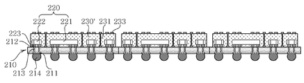
도 3은 본 발명의 제1 실시예에 따른 반도체 모듈의 구조도이다.3 is a structural diagram of a semiconductor module according to a first embodiment of the present invention.
도 3을 참조하면, 본 발명의 제1 실시예에 따른 반도체 모듈은 기저 기판(110)과, 기저 기판(110)에 실장되는 제1 실장 소자(120), 제1 실장 소자(120)를 에워싸게 형성된 제1 몰딩층(130), 제1 몰딩층(130)에 실장된 제2 실장 소자(140) 및 제2 실장 소자를 에워싸도록 형성된 제2 몰딩층(150)으로 이루어져 있다.Referring to FIG. 3, the semiconductor module according to the first embodiment of the present invention surrounds the
여기에서, 기저 기판(110)은 배선 기판으로, HTCC(High temperature cofired ceramic) 혹은 LTCC(Low temperature co-fired ceramic)와 같은 세라믹 기판이나 PCB 기판 등을 포함한다. Here, the
그리고, 기저 기판(110)의 표면에는 사전에 설계된 본딩 패드(111)나 범프 패드(112) 등을 포함한 배선패턴이 형성되어 있으며, 내부에는 비아홀(via hole)(113)이나 쓰루홀(Through hole) 등 이 형성되어 있어 실장되는 실장 소자(120, 140)의 신호라인을 구성하게 된다.In addition, a wiring pattern including a previously designed
또한, 이러한 기저 기판(110)의 일면에는 본딩 패드(111)에 접속된 솔더볼(114)이 어레이 형상으로 배열되어 있으며 이와 같은 솔더볼(114)을 통하여 모기판(미도시)에 실장된다.In addition, the
다음으로, 기저 기판(110)에 실장되는 제1 실장 소자(120)로는 반도체 소자(121)와, 수동소자(122)가 있으며, 반도체 소자(121)는 예를 들면, 트랜지스터, 다이오드, IC 칩 등이고, 수동 소자(122)는 예를 들면, 칩 콘덴서, 칩 저항 등이다.Next, the
이러한 제1 실장 소자(120)는 기저 기판(110)에 접하는 면에 범프 패드(123)를 구비하여 기저 기판(110)에 구비된 범프 패드(112)와 플립칩 본딩을 수행하여 접속된다. 물론, 제1 실장 소자(120)와 기저 기판(110)은 와이어 본딩등을 사용하여 접속될 수도 있다. The
이와 같은 제1 실장 소자(120)를 에워싸도록 제1 몰딩층(130)이 형성되어 있으며, 몰딩층(130)은 가열함으로써 연화하는 재료는 어떠한 것이든 이용할 수 있다.The
일예로, 제1 몰딩층(130)의 재료로는 에폭시 수지, BT 레진 등의 멜라민 유도체, 액정 폴리머, PPE수지, 폴리이미드 수지, 불소 수지, 페놀 수지, 폴리아미드 비스말레이미드 등을 이용할 수 있다. 이러한 수지를 이용함으로써, 고주파 특성이나 제품 신뢰성이 뛰어난 반도체 모듈을 얻을 수 있다.For example, the material of the
에폭시 수지로서는, 비스페놀 A형 수지, 비스페놀 F형 수지, 비스페놀 S형 수지, 페놀 노볼락 수지, 크레졸 노볼락형 에폭시 수지, 트리스 페놀 메탄형 에폭시 수지, 지환식 에폭시 수지 등을 들 수 있다.Examples of the epoxy resins include bisphenol A resins, bisphenol F resins, bisphenol S resins, phenol novolac resins, cresol novolac epoxy resins, trisphenol methane type epoxy resins, and alicyclic epoxy resins.
멜라민 유도체로서는, 멜라민, 멜라민 시아누레이트, 메틸올화 멜라민, (이소)시아누르산, 멜람, 멜럼, 멜롬, 석시노구아민,황산 멜라민, 황산 아세트 구아나민, 황산 멜람, 황산 구아닐 멜라민, 멜라민 수지, BT 레진, 시아누르산, 이소시아누르산,이소시아누르산 유도체, 멜라민 이소시아누레이트, 벤조 구아나민, 아세토구아나민 등의 멜라민 유도체, 구아니진계 화합물 등이 예시된다.As melamine derivatives, melamine, melamine cyanurate, methylolated melamine, (iso) cyanuric acid, melam, melum, melom, succinoguamine, melamine sulfate, sulfate acet guanamine, melamine sulfate, guanyl melamine sulfate, melamine resin , Melamine derivatives such as BT resin, cyanuric acid, isocyanuric acid, isocyanuric acid derivatives, melamine isocyanurate, benzoguanamine, acetoguanamine, and guanigin compounds.
액정 폴리머로서는, 방향족계 액정 폴리에스테르, 폴리이미드, 폴리에스테르 아미드나, 그것들을 함유하는 수지 조성물이 예시된다.As a liquid crystal polymer, aromatic liquid crystalline polyester, polyimide, polyester amide, and the resin composition containing them are illustrated.
또한, 제1 몰딩층(120)은 필러 또는 섬유 등의 충전재를 포함할 수 있다. 필러로서는, 예를 들면 입자 형상 또는 섬유형상의 SiO2, SiN, AlN이나 Al2O3 등을 이용할 수 있다. 제1 몰딩층(120)에 필러나 섬유를 포함함으로써, 제1 몰딩층(120)을 예를 들면 실온으로 냉각할 때에, 휘어짐을 저감할 수 있다. In addition, the
이에 따라, 반도체 소자(121) 및 수동 소자(122)와 제1 몰딩층(130)과의 밀착성을 높일 수 있다. 또한, 제1 몰딩층(130)에 섬유를 포함한 경우, 유동성을 높일 수 있기 때문에, 제1 몰딩층(130)과 반도체 소자(121) 및 수동 소자(122)와의 밀착성을 높일 수 있다. As a result, adhesion between the
그리고, 제1 몰딩층(130)의 내부에는 기저기판(110)의 표면에 형성된 배선패턴과 제1 몰딩층(130)에 적층되는 제2 실장 소자(140)간의 전기적 접속을 제공하는 다수의 비아홀(131)이 형성되어 있으며, 외부 표면에는 제2 실장 소자(140)가 실장될 수 있도록 범프 패드(132)를 포함한 배선패턴이 형성되어 있다.In addition, a plurality of via holes are provided in the
이처럼 외부 표면에 범프 패드(132)가 형성된 제1 몰딩층(130)의 상부에 제1 몰딩층(130)에 접하는 면에 구비된 범프 패드(143)를 이용하여 제2 실장 소자(140)가 플립칩 본딩에 의하여 실장된다. 물론 제1 몰딩층(130)에 형성된 범프 패드(132)와 제2 실장 소자(140)는 와이어 본딩 등을 통하여 연결될 수도 있다.As described above, the
상기 제2 실장 소자(140) 또한 반도체 소자(141)나 수동소자(142)일 수 있으며, 반도체 소자(141)는 예를 들면, 트랜지스터, 다이오드, IC 칩 등이고, 수동 소자(142)는 예를 들면, 칩 콘덴서, 칩 저항 등일 수 있다.The
다음으로, 제1 몰딩층(130)의 표면에 적층된 제2 실장 소자(140)를 둘러싸도록 에폭시 수지, BT 레진 등의 멜라민 유도체, 액정 폴리머, PPE수지, 폴리이미드 수지, 불소 수지, 페놀 수지, 폴리아미드 비스말레이미드 등과 같은 몰딩 물질로 이루어진 제2 몰딩층(150)이 형성되어 있다.Next, an epoxy resin, melamine derivatives such as BT resin, a liquid crystal polymer, a PPE resin, a polyimide resin, a fluorine resin, and a phenol resin so as to surround the second mounting
이와 같은 제2 몰딩층(150)은 필러 또는 섬유 등의 충전재를 포함할 수 있다. 이와 같은 제2 몰딩층(150)으로 인하여 제2 실장 소자(140)는 외부의 충격이나 오염 등으로부터 보호받는다.The
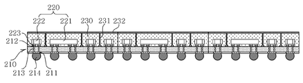
도 4는 본 발명의 제2 실시예에 따른 반도체 모듈의 구조도이다. 4 is a structural diagram of a semiconductor module according to a second embodiment of the present invention.
도 4의 제2 실시예가 도 3의 제1 실시예의 반도체 모듈의 구조와 다른 점은 제2 몰딩층(150')이 제2 실장 소자(140) 뿐만 아니라 제1 몰딩층(130')도 에워싸도록 형성되어 있다는 점이다.The second embodiment of FIG. 4 differs from the structure of the semiconductor module of the first embodiment of FIG. 3 in that the
이처럼 제2 몰딩층(150')이 제2 실장 소자(140) 뿐만 아니라 제1 몰딩층(130')도 에워싸도록 형성하기 위해서는 제1 몰딩층(130')이 기저 기판(110)의 일부를 남겨놓고 몰딩을 수행하여야 하며, 이에 따라 나머지 부분은 제2 몰딩층(150')이 보호하도록 형성된다.As such, in order to form the
이렇게 한다면, 제1 실시예와 달리 제1 몰딩층(130')과 제2 실장 소자(140)의 결속을 강화할 수 있으며, 제2 몰딩층(150')이 전체를 에워싸도록 일체로 형성되기 때문에 외부 충격등으로부터 내부 실장 소자를 더 잘 보호할 수 있다. 그외 구성요소는 제1 실시예와 동일하여 상세한 설명은 생략한다.In this case, unlike the first embodiment, the bonding between the
도 5는 본 발명의 제3 실시예에 따른 반도체 모듈의 구조도이다.5 is a structural diagram of a semiconductor module according to a third embodiment of the present invention.
도 5의 제3 실시예가 도 3의 제1 실시예의 반도체 모듈의 구조와 다른 점은 제2 실장 소자(140)를 보호하기 위하여 캡(160)을 사용하고 있다는 점이다. The third embodiment of FIG. 5 differs from the structure of the semiconductor module of the first embodiment of FIG. 3 in that the
상기 캡(160)은 전자파 차폐 수단을 설치하기 위한 대상이 되는 제 2 실장 소자(140)의 둘레를 둘러싸도록 형성되어 있다. 이러한 캡(160)은 금속 또는 도전성 재질로 구성된다. 그외의 점에 있어서는 제1 실시예와 동일하여 상세한 설명은 생략한다.The
도 6은 본 발명의 제4 실시예에 따른 반도체 모듈의 구조도이다.6 is a structural diagram of a semiconductor module according to a fourth embodiment of the present invention.
도 6의 제4 실시예가 도 5의 제 3 실시예와 다른 점은 캡(160')이 제2 실장 소자(140) 뿐만 아니라 제1 몰딩층(120')도 에워싸도록 형성되어 있다는 점이다.The fourth embodiment of FIG. 6 differs from the third embodiment of FIG. 5 in that the
이처럼 캡(160')이 제2 실장 소자(140) 뿐만 아니라 제1 몰딩층(130')도 에워싸도록 형성하기 위해서는 제1 몰딩층(130')이 기저 기판(110)의 일부를 남겨놓고 몰딩을 수행하여야 하며, 이에 따라 나머지 부분은 캡(160')이 보호하도록 형성된다. 그외 구성요소는 제1 실시예와 동일하여 상세한 설명은 생략한다.As such, in order to form the
도 7 내지 도 15는 본 발명의 제1 실시예에 따른 반도체 모듈의 제조 방법을 나타낸 단면도이다.7 to 15 are cross-sectional views illustrating a method of manufacturing a semiconductor module in accordance with a first embodiment of the present invention.
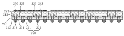
우선, 도 7에 도시되어 있는 바와 같이, 배선 기판으로 표면에 사전에 설계된 본딩 패드(211), 범프 패드(212) 등을 포함한 배선패턴이 형성되어 있거나, 내부에 비아홀(via hole)(213) 등이 형성되어 있는 기저 기판(210)을 준비한다.First, as shown in FIG. 7, a wiring pattern including a
이러한 기저 기판(210)의 일면에는 본딩 패드(211)에 접속된 솔더볼(214)이 어레이 형상으로 배열되어 있으며 이와 같은 솔더볼(214)을 통하여 이후에 모기판(미도시)에 실장된다.
다음으로, 도 8에 도시하는 바와 같이, 기저 기판(210) 상에 복수의 반도체 소자(221)나 수동 소자(222) 등의 실장 소자(220)를 고정한다. Next, as shown in FIG. 8, mounting
여기에서, 기저 기판(210)에 실장 소자(220)를 실장하는 방법은 플립칩 방식을 사용할 수 있으며, 도시되지는 않았지만 와이어 본딩 방식으로 실장할 수 있다.Here, a method of mounting the mounting
여기에서, 반도체 소자(221)는 예를 들면, 트랜지스터, 다이오드, IC 칩 등이다. 또한, 수동 소자(222)는, 예를 들면, 칩 콘덴서, 칩 저항 등이다.Here, the
다음으로, 도 9에 도시하는 바와 같이, 복수의 반도체 소자 및 수동 소자를 고정한 상태에서, 몰딩 물질로 제1 실장 소자(220)를 에워싸도록 몰딩을 수행하여 제1 몰딩층(230)을 형성한다.Next, as shown in FIG. 9, in a state in which a plurality of semiconductor devices and passive devices are fixed, molding is performed to surround the
이때, 제1 몰딩층(230)을 형성하기 위하여 사용가능한 방법으로는 트랜스퍼 몰딩, 인젝션 몰딩, 포팅 또는 디핑 등을 이용하여 형성될 수 있으며, 몰딩 재질로는 예를 들면 에폭시 수지, BT 레진 등의 멜라민 유도체, 액정 폴리머, PPE수지, 폴리이미드 수지, 불소 수지, 페놀 수지, 폴리아미드 비스말레이미드 등을 이용할 수 있다. 이러한 수지를 이용함으로써, 고주파 특성이나 제품 신뢰성이 뛰어난 반도체 모듈을 얻을 수 있다.In this case, a method usable for forming the
또한, 몰딩층(230)은 필러 또는 섬유 등의 충전재를 포함할 수 있다. In addition, the
이후에, 도 10에 도시된 바와 같이 제1 몰딩층(230)에 레이저 등을 사용하여 홀을 형성하고, 형성된 홀 내를 전도성 페이스트 등의 전도성 재료로 매립하여 비아홀(231)을 형성한다. Thereafter, as shown in FIG. 10, a hole is formed in the
계속하여, 도 11에 도시된 바와 같이 제1 몰딩층(230)에 도전층(232)을 형성하고 도 12에 도시된 바와 같이 패터닝하여 복수의 반도체 소자(221) 및 수동 소자(222) 사이를 전기적으로 접속을 제공하거나 범프 패드(233)를 형성하여 외부와 전기적 접속을 제공할 수 있도록 한다. Subsequently, as shown in FIG. 11, the
그 후, 도 13에 도시하는 바와 같이 제1 몰딩층(230)의 상면에 형성된 범프 패드(233)에 제2 실장 소자(240)의 범프 패드(243)가 접하도록 적층하여 제2 실장 소자가 실장되도록 한다.After that, as illustrated in FIG. 13, the
이때, 제1 몰딩층(230)에 실장되는 제2 실장 소자(240)는 트랜지스터, 다이오드, IC 칩 등의 반도체 소자이거나, 칩 콘덴서, 칩 저항 등의 수동소자일 수 있다.In this case, the
그리고, 도 14에 도시된 바와 같이 일예로 에폭시 수지, BT 레진 등의 멜라민 유도체, 액정 폴리머, PPE수지, 폴리이미드 수지, 불소 수지, 페놀 수지, 폴리아미드 비스말레이미드 등의 몰딩 물질로 구성된 제2 몰딩층(250)을 형성하여 외부로부터 보호되도록 한다. And, as shown in FIG. 14, for example, a second material composed of a molding material such as an epoxy resin, melamine derivatives such as BT resin, a liquid crystal polymer, a PPE resin, a polyimide resin, a fluorine resin, a phenol resin, and a polyamide bismaleimide The
이후에, 도 15에 도시된 바와 같이 컷팅 칼이나 레이저 등을 사용하여 다이싱을 하여 반도체 모듈별로 분리되도록 한다.Thereafter, as illustrated in FIG. 15, dicing is performed using a cutting knife or a laser to separate the semiconductor modules.
다음으로, 도 16 내지 도 24는 본 발명의 제2 실시예에 따른 반도체 모듈의 제조 방법의 단면도이다.16 to 24 are cross-sectional views of a method of manufacturing a semiconductor module according to the second embodiment of the present invention.
도 16 내지 도 24에 도시된 반도체 모듈이 제1 실시예에 개시된 반도체 모듈의 제조방법과 다른 점은, 도 18에 도시된 바와 같이 제1 몰딩층(230')을 형성할 때 기저 기판(210)의 전체에 형성되도록 하지 않고 여유 공간이 생성되도록 하고, 도 23에 도시된 바와 같이 제2 몰딩층(250')을 형성할 때 제2 실장 소자(240)뿐만 아니라 제1 몰딩층(230')도 에워싸도록 형성한다는 점이다.16 to 24 is different from the manufacturing method of the semiconductor module disclosed in the first embodiment, the
그외, 배선 기판으로 사전에 설계된 본딩 패드(211), 범프 패드(212). 비아홀(via hole)(213), 솔더볼(214)이 형성되어 있는 기저 기판(210)을 준비하는 단계(도 16 참조), 기저 기판(210) 상에 복수의 반도체 소자(221)나 수동 소자(222) 등의 실장 소자(220)을 고정하는 단계(도 17 참조), 제1 몰딩층(230')에 비아홀(231)을 형성하는 단계(도 19참조), 제1 몰딩층(230')에 도전층(232)를 형성하는 단계(도 20 참조), 범프 패드(233)를 형성하는 단계(도 21 참조), 제1 몰딩층(230')에 제2 실장 소자(240)의 범프 패드(243)가 접하도록 하여 제2 실장 소자를 실장하는 단계(도 22 참조), 반도체 모듈별로 다이싱하는 단계(도 24 참조) 등이 제1 실시예와 유사하기 때문에 그에 대한 구체적인 설명은 생략한다.In addition,
도 25~도 33은 본 발명의 제3 실시예에 따른 반도체 모듈의 제조 방법을 나타낸 단면도이다.25 to 33 are cross-sectional views illustrating a method of manufacturing a semiconductor module in accordance with a third embodiment of the present invention.
도 25 내지 33의 제3 실시예가 제1 실시예의 반도체 모듈의 제조 방법과 다른 점은 제2 실장 소자(240)를 보호하기 위하여 캡(260)을 사용하고 있다는 점이다. The third embodiment of FIGS. 25 to 33 differs from the manufacturing method of the semiconductor module of the first embodiment in that the
상기 캡(260)은 도 32에 도시된 바와 같이 전자파 차폐 수단을 설치하기 위한 대상이 되는 제 2 실장 소자(240)의 둘레를 둘러싸도록 형성되어 있다. 이러한 캡(260)은 금속 또는 도전성 재질로 구성된다. As shown in FIG. 32, the
그외, 배선 기판으로 사전에 설계된 본딩 패드(211), 범프 패드(212). 비아홀(via hole)(213), 솔더볼(214)가 형성되어 있는 기저 기판(210)을 준비하는 단계(도 25 참조), 기저 기판(210) 상에 복수의 반도체 소자(221)나 수동 소자(222) 등의 실장 소자(220)을 고정하는 단계(도 26 참조), 복수의 반도체 소자 및 수동 소자를 고정한 상태에서, 몰딩 물질로 제1 실장 소자(220)를 에워싸도록 몰딩을 수행하여 몰딩층(230)을 형성하는 단계(도 27 참조),제1 몰딩층(230)에 비아홀(231)을 형성하는 단계(도 28 참조), 제1 몰딩층(230)에 도전층(232)를 형성하는 단계(도 29 참조), 범프 패드(233)를 형성하는 단계(도 30 참조), 제1 몰딩층(230)에 제2 실장 소자(240)의 범프 패드(243)가 접하도록 하여 제2 실장 소자를 실장하는 단계(도 31 참조), 반도체 모듈별로 다이싱하는 단계(도 33 참조) 등이 제1 실시예와 유사하기 때문에 그에 대한 구체적인 설명은 생략한다.In addition,
도 34~도 42는 본 발명의 제4 실시예에 따른 반도체 모듈의 제조 방법을 나타낸 단면도이다.34 to 42 are cross-sectional views illustrating a method of manufacturing a semiconductor module in accordance with a fourth embodiment of the present invention.
도 34 내지 43의 제4 실시예에 따른 반도체 모듈의 제조 방법이 도 25 내지 33의 제3 실시예에 따른 반도체 모듈의 제조 방법과 다른 점은 도 41에 도시된 바와 같이 캡(260')이 제2 실장 소자(240)에 더해 제1 몰딩층(230')을 에워싸도록 형성된다는 점이다.The manufacturing method of the semiconductor module according to the fourth embodiment of FIGS. 34 to 43 is different from the manufacturing method of the semiconductor module according to the third embodiment of FIGS. 25 to 33, as shown in FIG. 41. It is formed to surround the
이를 위하여, 제1 실시예와 다르게 도 36에 도시된 바와 같이 제1 몰딩층(230')을 형성할 때 기저기판(210)의 전체에 형성하는 것이 아니라 일부를 남겨놓고 나머지 부분에 형성한다.To this end, unlike the first embodiment, when forming the
그리고, 도 41에 도시된 바와 같이 캡(260')을 형성할 때 제1 실시예와 달리 제1 몰딩층을 포함하여 제2 실장 소자를 에워싸도록 형성한다.As shown in FIG. 41, when the
그외, 배선 기판으로 사전에 설계된 본딩 패드(211), 범프 패드(212). 비아홀(via hole)(213), 솔더볼(214)가 형성되어 있는 기저 기판(210)을 준비하는 단계(도 34 참조), 기저 기판(210) 상에 복수의 반도체 소자(221)나 수동 소자(222) 등의 실장 소자(220)을 고정하는 단계(도 35 참조), 제1 몰딩층(230')에 비아홀(231)을 형성하는 단계(도 37참조), 제1 몰딩층(230')에 도전층(232)를 형성하는 단계(도 38 참조), 범프 패드(233)를 형성하는 단계(도 39 참조), 제1 몰딩층(230')에 제2 실장 소자를 실장하는 단계(도 40 참조), 반도체 모듈별로 다이싱하는 단계(도 42 참조) 등이 제1 실시예와 유사하기 때문에 그에 대한 구체적인 설명은 생략한다.
In addition,
110, 210 : 기저 기판 111, 211 : 본딩패드
112, 212 : 범프 패드 113, 213 : 비아홀
114, 214 : 솔더볼 120, 220 : 제1 실장 소자
121, 221 : 반도체 소자 122, 222 : 수동 소자
123, 223 : 범프 패드 130, 130', 230, 230' : 제1 몰딩층
131, 231 : 비아홀 132, 233 : 범프패드
140, 240 : 제2 실장 소자 141, 214 : 반도체 소자
142, 242 : 수동 소자 243 : 범프 패드
150, 150', 250, 250' : 제2 몰딩층
160, 160', 260, 260' : 캡 110, 210:
112, 212: bump
114 and 214:
121, 221:
123 and 223: bump
131, 231: via
140 and 240: second mounting
142, 242: passive element 243: bump pad
150, 150 ', 250, 250': second molding layer
160, 160 ', 260, 260': cap
Claims (19)
상기 기저기판위에 실장되어 있는 제1 실장 소자;
몰딩 물질로 상기 실장 소자를 에워싸도록 형성되어 있으며 내부에 비아홀을 구비하여 상기 기저기판의 일측 표면에 형성되어 있는 배선패턴과 인터커넥션을 제공하는 제1 몰딩층; 및
상기 제1 몰딩층에 접촉면이 모두 위치하도록 실장되어 있으며,상기 제1 몰딩층에 형성된 비아홀을 통하여 상기 기저 기판의 일측 표면에 형성되어 있는 배선패턴과 전기적으로 접속되는 제2 실장 소자를 포함하는 반도체 모듈.A base substrate having wiring patterns formed on both surfaces thereof;
A first mounting element mounted on the base substrate;
A first molding layer formed to surround the mounting device with a molding material and having a via hole therein to provide interconnection patterns and interconnections formed on one surface of the base substrate; And
A semiconductor including a second mounting element electrically connected to the first molding layer, the second mounting element being electrically connected to a wiring pattern formed on one surface of the base substrate through a via hole formed in the first molding layer; module.
상기 제1 몰딩층의 몰딩 물질은 에폭시 수지, 멜라민 유도체, 액정 폴리머, PPE수지, 폴리이미드 수지, 불소 수지, 페놀 수지, 폴리아미드 비스말레이미드 중 어느 하나로 구성된 것을 특징으로 하는 반도체 모듈.The method according to claim 1,
The molding material of the first molding layer is a semiconductor module, characterized in that composed of any one of an epoxy resin, melamine derivatives, liquid crystal polymer, PPE resin, polyimide resin, fluorine resin, phenol resin, polyamide bismaleimide.
몰딩 물질로 상기 제2 실장 소자를 에워싸도록 형성된 제2 몰딩층을 더 포함하는 반도체 모듈.The method according to claim 1,
And a second molding layer formed to surround the second mounting device with a molding material.
상기 제2 몰딩층의 몰딩 물질은 에폭시 수지, 멜라민 유도체, 액정 폴리머, PPE수지, 폴리이미드 수지, 불소 수지, 페놀 수지, 폴리아미드 비스말레이미드 중 어느 하나로 구성된 것을 특징으로 하는 반도체 모듈.The method according to claim 3,
The molding material of the second molding layer is a semiconductor module, characterized in that composed of any one of an epoxy resin, melamine derivatives, liquid crystal polymer, PPE resin, polyimide resin, fluorine resin, phenol resin, polyamide bismaleimide.
몰딩 물질로 상기 제1 몰딩층과 상기 제2 실장 소자를 에워싸도록 형성된 제2 몰딩층을 더 포함하는 반도체 모듈.The method according to claim 1,
And a second molding layer formed to surround the first molding layer and the second mounting device with a molding material.
상기 제2 몰딩층의 몰딩 물질은 에폭시 수지, 멜라민 유도체, 액정 폴리머, PPE수지, 폴리이미드 수지, 불소 수지, 페놀 수지, 폴리아미드 비스말레이미드 중 어느 하나로 구성된 것을 특징으로 하는 반도체 모듈.The method according to claim 5,
The molding material of the second molding layer is a semiconductor module, characterized in that composed of any one of an epoxy resin, melamine derivatives, liquid crystal polymer, PPE resin, polyimide resin, fluorine resin, phenol resin, polyamide bismaleimide.
상기 제2 실장 소자를 에워싸도록 형성된 캡을 더 포함하는 반도체 모듈.The method according to claim 1,
And a cap formed to surround the second mounting element.
상기 제1 몰딩층과 상기 제2 실장 소자를 에워싸도록 형성된 캡을 더 포함하는 반도체 모듈.The method according to claim 1,
And a cap formed to surround the first molding layer and the second mounting device.
상기 제1 실장 소자는 반도체 소자와 수동 소자로 이루어진 것을 특징으로 하는 반도체 모듈.The method according to claim 1,
The first mounting device is a semiconductor module, characterized in that consisting of a semiconductor device and a passive device.
상기 제2 실장 소자는 반도체 소자와 수동 소자로 이루어진 것을 특징으로 하는 반도체 모듈.The method according to claim 1,
The second mounting device is a semiconductor module, characterized in that consisting of a semiconductor device and a passive device.
(B) 상기 제1 실장 소자가 실장된 기저기판 위에 제1 몰딩층을 형성하는 단계;
(C) 상기 제1 몰딩층에 인터커넥션을 위한 비아홀을 형성하는 단계; 및
(D) 상기 비아홀을 이용하여 상기 기저기판의 일측 표면에 형성되어 있는 배선패턴과 접속되도록 제2 실장 소자를 상기 제1 몰딩층내에 접촉면이 모두 위치하도록 실장하는 단계를 포함하는 반도체 모듈의 제조방법.(A) mounting a first mounting device after preparing a base substrate having wiring patterns formed on both surfaces thereof;
(B) forming a first molding layer on the base substrate on which the first mounting device is mounted;
(C) forming via holes for interconnection in the first molding layer; And
(D) manufacturing a semiconductor module comprising mounting the second mounting element such that all of the contact surfaces are located in the first molding layer so as to be connected to a wiring pattern formed on one surface of the base substrate by using the via hole. .
상기 제1 몰딩층의 몰딩 물질은 에폭시 수지, 멜라민 유도체, 액정 폴리머, PPE수지, 폴리이미드 수지, 불소 수지, 페놀 수지, 폴리아미드 비스말레이미드 중 어느 하나로 구성된 것을 특징으로 하는 반도체 모듈의 제조방법.The method of claim 11,
The molding material of the first molding layer is a semiconductor module manufacturing method, characterized in that composed of any one of an epoxy resin, melamine derivatives, liquid crystal polymer, PPE resin, polyimide resin, fluorine resin, phenol resin, polyamide bismaleimide.
(E) 몰딩 물질로 상기 제2 실장 소자를 에워싸도록 제2 몰딩층을 형성하는 단계를 더 포함하는 반도체 모듈의 제조방법.The method of claim 11,
(E) forming a second molding layer to surround the second mounting device with a molding material.
상기 제2 몰딩층의 몰딩 물질은 에폭시 수지, 멜라민 유도체, 액정 폴리머, PPE수지, 폴리이미드 수지, 불소 수지, 페놀 수지, 폴리아미드 비스말레이미드 중 어느 하나로 구성된 것을 특징으로 하는 반도체 모듈의 제조방법.The method according to claim 13,
The molding material of the second molding layer is a semiconductor module manufacturing method, characterized in that composed of any one of an epoxy resin, melamine derivatives, liquid crystal polymer, PPE resin, polyimide resin, fluorine resin, phenol resin, polyamide bismaleimide.
(E) 몰딩 물질로 상기 제1 몰딩층과 상기 제2 실장 소자를 에워싸도록 제2 몰딩층을 형성하는 단계를 더 포함하는 반도체 모듈의 제조방법.The method of claim 11,
(E) forming a second molding layer with a molding material to surround the first molding layer and the second mounting device.
상기 제2 몰딩층의 몰딩 물질은 에폭시 수지, 멜라민 유도체, 액정 폴리머, PPE수지, 폴리이미드 수지, 불소 수지, 페놀 수지, 폴리아미드 비스말레이미드 중 어느 하나로 구성된 것을 특징으로 하는 반도체 모듈의 제조방법.The method according to claim 15,
The molding material of the second molding layer is a semiconductor module manufacturing method, characterized in that composed of any one of an epoxy resin, melamine derivatives, liquid crystal polymer, PPE resin, polyimide resin, fluorine resin, phenol resin, polyamide bismaleimide.
(E) 상기 제2 실장 소자를 에워싸도록 캡을 형성하는 단계를 더 포함하는 반도체 모듈의 제조방법.The method of claim 11,
(E) forming a cap so as to surround the second mounting element.
(E) 상기 제1 몰딩층과 상기 제2 실장 소자를 에워싸도록 캡을 형성하는 단계를 더 포함하는 반도체 모듈의 제조방법.The method of claim 11,
(E) forming a cap so as to surround the first molding layer and the second mounting element.
상기 (C)단계는,
(C-1) 상기 제1 몰딩층에 레이저를 사용하여 홀을 형성하는 단계; 및
(C-2) 상기 제1 몰딩층에 형성된 홀 내를 전도성 페이스트를 충진하여 비아홀을 형성하는 단계를 포함하는 반도체 모듈의 제조방법.In claim 11
Step (C) is,
(C-1) forming a hole in the first molding layer using a laser; And
(C-2) A method of manufacturing a semiconductor module comprising filling a conductive paste in a hole formed in the first molding layer to form a via hole.
Priority Applications (2)
| Application Number | Priority Date | Filing Date | Title |
|---|---|---|---|
| KR1020100071506A KR101119348B1 (en) | 2010-07-23 | 2010-07-23 | Semiconductor module and manufactureing method thereof |
| US12/897,222 US20120018897A1 (en) | 2010-07-23 | 2010-10-04 | Semiconductor module and method of manufacturing the same |
Applications Claiming Priority (1)
| Application Number | Priority Date | Filing Date | Title |
|---|---|---|---|
| KR1020100071506A KR101119348B1 (en) | 2010-07-23 | 2010-07-23 | Semiconductor module and manufactureing method thereof |
Publications (2)
| Publication Number | Publication Date |
|---|---|
| KR20120010021A KR20120010021A (en) | 2012-02-02 |
| KR101119348B1 true KR101119348B1 (en) | 2012-03-07 |
Family
ID=45492937
Family Applications (1)
| Application Number | Title | Priority Date | Filing Date |
|---|---|---|---|
| KR1020100071506A Expired - Fee Related KR101119348B1 (en) | 2010-07-23 | 2010-07-23 | Semiconductor module and manufactureing method thereof |
Country Status (2)
| Country | Link |
|---|---|
| US (1) | US20120018897A1 (en) |
| KR (1) | KR101119348B1 (en) |
Families Citing this family (21)
| Publication number | Priority date | Publication date | Assignee | Title |
|---|---|---|---|---|
| US9064879B2 (en) | 2010-10-14 | 2015-06-23 | Taiwan Semiconductor Manufacturing Company, Ltd. | Packaging methods and structures using a die attach film |
| US8936966B2 (en) | 2012-02-08 | 2015-01-20 | Taiwan Semiconductor Manufacturing Company, Ltd. | Packaging methods for semiconductor devices |
| US8105875B1 (en) | 2010-10-14 | 2012-01-31 | Taiwan Semiconductor Manufacturing Company, Ltd. | Approach for bonding dies onto interposers |
| US10192796B2 (en) | 2012-09-14 | 2019-01-29 | STATS ChipPAC Pte. Ltd. | Semiconductor device and method of forming dual-sided interconnect structures in FO-WLCSP |
| US9818734B2 (en) | 2012-09-14 | 2017-11-14 | STATS ChipPAC Pte. Ltd. | Semiconductor device and method of forming build-up interconnect structures over a temporary substrate |
| US8890284B2 (en) * | 2013-02-22 | 2014-11-18 | Infineon Technologies Ag | Semiconductor device |
| US8927412B1 (en) * | 2013-08-01 | 2015-01-06 | Taiwan Semiconductor Manufacturing Company, Ltd. | Multi-chip package and method of formation |
| US9910145B2 (en) * | 2013-12-19 | 2018-03-06 | Infineon Technologies Ag | Wireless communication system, a radar system and a method for determining a position information of an object |
| US9368455B2 (en) * | 2014-03-28 | 2016-06-14 | Intel Corporation | Electromagnetic interference shield for semiconductor chip packages |
| KR101656269B1 (en) | 2014-12-30 | 2016-09-12 | 주식회사 네패스 | Semiconductor package and manufacturing method thereof |
| US9893017B2 (en) * | 2015-04-09 | 2018-02-13 | STATS ChipPAC Pte. Ltd. | Double-sided semiconductor package and dual-mold method of making same |
| US9773764B2 (en) * | 2015-12-22 | 2017-09-26 | Intel Corporation | Solid state device miniaturization |
| CN107910310B (en) * | 2017-12-28 | 2023-09-12 | 江阴长电先进封装有限公司 | A multi-chip fan-out packaging structure and packaging method thereof |
| JP2020004886A (en) * | 2018-06-29 | 2020-01-09 | 太陽誘電株式会社 | Semiconductor module |
| US11335712B2 (en) * | 2019-05-13 | 2022-05-17 | Boe Technology Group Co., Ltd. | Array substrate, display apparatus, and method of fabricating array substrate |
| US10849235B1 (en) * | 2020-05-20 | 2020-11-24 | Tactotek Oy | Method of manufacture of a structure and structure |
| US11610847B2 (en) * | 2021-05-07 | 2023-03-21 | STATS ChipPAC Pte. Ltd. | Laser-based redistribution and multi-stacked packages |
| US11749668B2 (en) | 2021-06-09 | 2023-09-05 | STATS ChipPAC Pte. Ltd | PSPI-based patterning method for RDL |
| US12564059B2 (en) | 2022-10-12 | 2026-02-24 | STATS ChipPAC Pte. Ltd. | Semiconductor device and method of forming graphene core shell embedded within shielding layer |
| US12581974B2 (en) | 2023-01-05 | 2026-03-17 | STATS ChipPAC Pte. Ltd. | Semiconductor device and method of making a semiconductor package with graphene-coated interconnects |
| US12588572B2 (en) | 2023-03-15 | 2026-03-24 | STATS ChipPAC Pte. Ltd. | Semiconductor device and method of forming fine pitch conductive posts with graphene-coated cores |
Citations (2)
| Publication number | Priority date | Publication date | Assignee | Title |
|---|---|---|---|---|
| KR100442880B1 (en) | 2002-07-24 | 2004-08-02 | 삼성전자주식회사 | Stacked semiconductor module and manufacturing method thereof |
| KR100800478B1 (en) | 2006-07-18 | 2008-02-04 | 삼성전자주식회사 | Multilayer semiconductor package and manufacturing method thereof |
Family Cites Families (7)
| Publication number | Priority date | Publication date | Assignee | Title |
|---|---|---|---|---|
| US5468999A (en) * | 1994-05-26 | 1995-11-21 | Motorola, Inc. | Liquid encapsulated ball grid array semiconductor device with fine pitch wire bonding |
| US6930256B1 (en) * | 2002-05-01 | 2005-08-16 | Amkor Technology, Inc. | Integrated circuit substrate having laser-embedded conductive patterns and method therefor |
| US7633765B1 (en) * | 2004-03-23 | 2009-12-15 | Amkor Technology, Inc. | Semiconductor package including a top-surface metal layer for implementing circuit features |
| US7141874B2 (en) * | 2003-05-14 | 2006-11-28 | Matsushita Electric Industrial Co., Ltd. | Electronic component packaging structure and method for producing the same |
| US7528474B2 (en) * | 2005-05-31 | 2009-05-05 | Stats Chippac Ltd. | Stacked semiconductor package assembly having hollowed substrate |
| KR101329355B1 (en) * | 2007-08-31 | 2013-11-20 | 삼성전자주식회사 | stack-type semicondoctor package, method of forming the same and electronic system including the same |
| TWI473553B (en) * | 2008-07-03 | 2015-02-11 | 日月光半導體製造股份有限公司 | Chip package structure |
-
2010
- 2010-07-23 KR KR1020100071506A patent/KR101119348B1/en not_active Expired - Fee Related
- 2010-10-04 US US12/897,222 patent/US20120018897A1/en not_active Abandoned
Patent Citations (2)
| Publication number | Priority date | Publication date | Assignee | Title |
|---|---|---|---|---|
| KR100442880B1 (en) | 2002-07-24 | 2004-08-02 | 삼성전자주식회사 | Stacked semiconductor module and manufacturing method thereof |
| KR100800478B1 (en) | 2006-07-18 | 2008-02-04 | 삼성전자주식회사 | Multilayer semiconductor package and manufacturing method thereof |
Also Published As
| Publication number | Publication date |
|---|---|
| KR20120010021A (en) | 2012-02-02 |
| US20120018897A1 (en) | 2012-01-26 |
Similar Documents
| Publication | Publication Date | Title |
|---|---|---|
| KR101119348B1 (en) | Semiconductor module and manufactureing method thereof | |
| KR100692441B1 (en) | Semiconductor device and manufacturing method of semiconductor device | |
| US6492726B1 (en) | Chip scale packaging with multi-layer flip chip arrangement and ball grid array interconnection | |
| US9392698B2 (en) | Chip-embedded printed circuit board and semiconductor package using the PCB, and manufacturing method of the PCB | |
| US6396136B2 (en) | Ball grid package with multiple power/ground planes | |
| US20130292838A1 (en) | Package-on-package interconnect stiffener | |
| KR101942748B1 (en) | Fan-out semiconductor package | |
| KR20190090180A (en) | Electronic component package | |
| KR20190052598A (en) | Fan-out semiconductor package | |
| KR102099749B1 (en) | Fan-out semiconductor package | |
| KR20020061812A (en) | Ball grid array type multi chip package and stack package | |
| US10896877B1 (en) | System in package with double side mounted board | |
| US20170311447A1 (en) | Mechanically-compliant and electrically and thermally conductive leadframes for component-on-package circuits | |
| US6759753B2 (en) | Multi-chip package | |
| US20060091543A1 (en) | Land grid array module | |
| US8994157B1 (en) | Circuit system in a package | |
| US20050002167A1 (en) | Microelectronic package | |
| US6828671B2 (en) | Enhanced BGA grounded heatsink | |
| US7078791B1 (en) | Chip on board package for imager | |
| KR20090080701A (en) | Semiconductor package and laminated package using same | |
| US20160104652A1 (en) | Package structure and method of fabricating the same | |
| US9543277B1 (en) | Wafer level packages with mechanically decoupled fan-in and fan-out areas | |
| KR20150050189A (en) | Semiconductor Package | |
| KR100809254B1 (en) | Chip scale SIP module. | |
| KR20040063784A (en) | Semiconductor apparatus |
Legal Events
| Date | Code | Title | Description |
|---|---|---|---|
| A201 | Request for examination | ||
| PA0109 | Patent application |
St.27 status event code: A-0-1-A10-A12-nap-PA0109 |
|
| PA0201 | Request for examination |
St.27 status event code: A-1-2-D10-D11-exm-PA0201 |
|
| E902 | Notification of reason for refusal | ||
| PE0902 | Notice of grounds for rejection |
St.27 status event code: A-1-2-D10-D21-exm-PE0902 |
|
| P11-X000 | Amendment of application requested |
St.27 status event code: A-2-2-P10-P11-nap-X000 |
|
| P13-X000 | Application amended |
St.27 status event code: A-2-2-P10-P13-nap-X000 |
|
| E701 | Decision to grant or registration of patent right | ||
| PE0701 | Decision of registration |
St.27 status event code: A-1-2-D10-D22-exm-PE0701 |
|
| PG1501 | Laying open of application |
St.27 status event code: A-1-1-Q10-Q12-nap-PG1501 |
|
| GRNT | Written decision to grant | ||
| PR0701 | Registration of establishment |
St.27 status event code: A-2-4-F10-F11-exm-PR0701 |
|
| PR1002 | Payment of registration fee |
St.27 status event code: A-2-2-U10-U11-oth-PR1002 Fee payment year number: 1 |
|
| PG1601 | Publication of registration |
St.27 status event code: A-4-4-Q10-Q13-nap-PG1601 |
|
| R18-X000 | Changes to party contact information recorded |
St.27 status event code: A-5-5-R10-R18-oth-X000 |
|
| FPAY | Annual fee payment |
Payment date: 20150202 Year of fee payment: 4 |
|
| PR1001 | Payment of annual fee |
St.27 status event code: A-4-4-U10-U11-oth-PR1001 Fee payment year number: 4 |
|
| FPAY | Annual fee payment |
Payment date: 20160111 Year of fee payment: 5 |
|
| PR1001 | Payment of annual fee |
St.27 status event code: A-4-4-U10-U11-oth-PR1001 Fee payment year number: 5 |
|
| FPAY | Annual fee payment |
Payment date: 20170102 Year of fee payment: 6 |
|
| PR1001 | Payment of annual fee |
St.27 status event code: A-4-4-U10-U11-oth-PR1001 Fee payment year number: 6 |
|
| FPAY | Annual fee payment |
Payment date: 20180102 Year of fee payment: 7 |
|
| PR1001 | Payment of annual fee |
St.27 status event code: A-4-4-U10-U11-oth-PR1001 Fee payment year number: 7 |
|
| FPAY | Annual fee payment |
Payment date: 20190103 Year of fee payment: 8 |
|
| PR1001 | Payment of annual fee |
St.27 status event code: A-4-4-U10-U11-oth-PR1001 Fee payment year number: 8 |
|
| R18-X000 | Changes to party contact information recorded |
St.27 status event code: A-5-5-R10-R18-oth-X000 |
|
| FPAY | Annual fee payment |
Payment date: 20200102 Year of fee payment: 9 |
|
| PR1001 | Payment of annual fee |
St.27 status event code: A-4-4-U10-U11-oth-PR1001 Fee payment year number: 9 |
|
| PR1001 | Payment of annual fee |
St.27 status event code: A-4-4-U10-U11-oth-PR1001 Fee payment year number: 10 |
|
| PC1903 | Unpaid annual fee |
St.27 status event code: A-4-4-U10-U13-oth-PC1903 Not in force date: 20220216 Payment event data comment text: Termination Category : DEFAULT_OF_REGISTRATION_FEE |
|
| PC1903 | Unpaid annual fee |
St.27 status event code: N-4-6-H10-H13-oth-PC1903 Ip right cessation event data comment text: Termination Category : DEFAULT_OF_REGISTRATION_FEE Not in force date: 20220216 |
|
| P22-X000 | Classification modified |
St.27 status event code: A-4-4-P10-P22-nap-X000 |