KR101114412B1 - Optical sheet in which nano quantum dots are dispersed and backlight unit including the same - Google Patents
Optical sheet in which nano quantum dots are dispersed and backlight unit including the same Download PDFInfo
- Publication number
- KR101114412B1 KR101114412B1 KR1020110011812A KR20110011812A KR101114412B1 KR 101114412 B1 KR101114412 B1 KR 101114412B1 KR 1020110011812 A KR1020110011812 A KR 1020110011812A KR 20110011812 A KR20110011812 A KR 20110011812A KR 101114412 B1 KR101114412 B1 KR 101114412B1
- Authority
- KR
- South Korea
- Prior art keywords
- light
- guide plate
- optical sheet
- wavelength conversion
- light guide
- Prior art date
- Legal status (The legal status is an assumption and is not a legal conclusion. Google has not performed a legal analysis and makes no representation as to the accuracy of the status listed.)
- Active
Links
Images


Classifications
-
- G—PHYSICS
- G02—OPTICS
- G02B—OPTICAL ELEMENTS, SYSTEMS OR APPARATUS
- G02B5/00—Optical elements other than lenses
- G02B5/08—Mirrors
- G02B5/0808—Mirrors having a single reflecting layer
-
- B—PERFORMING OPERATIONS; TRANSPORTING
- B32—LAYERED PRODUCTS
- B32B—LAYERED PRODUCTS, i.e. PRODUCTS BUILT-UP OF STRATA OF FLAT OR NON-FLAT, e.g. CELLULAR OR HONEYCOMB, FORM
- B32B15/00—Layered products comprising a layer of metal
- B32B15/04—Layered products comprising a layer of metal comprising metal as the main or only constituent of a layer, which is next to another layer of the same or of a different material
- B32B15/08—Layered products comprising a layer of metal comprising metal as the main or only constituent of a layer, which is next to another layer of the same or of a different material of synthetic resin
-
- B—PERFORMING OPERATIONS; TRANSPORTING
- B82—NANOTECHNOLOGY
- B82Y—SPECIFIC USES OR APPLICATIONS OF NANOSTRUCTURES; MEASUREMENT OR ANALYSIS OF NANOSTRUCTURES; MANUFACTURE OR TREATMENT OF NANOSTRUCTURES
- B82Y20/00—Nanooptics, e.g. quantum optics or photonic crystals
-
- C—CHEMISTRY; METALLURGY
- C08—ORGANIC MACROMOLECULAR COMPOUNDS; THEIR PREPARATION OR CHEMICAL WORKING-UP; COMPOSITIONS BASED THEREON
- C08J—WORKING-UP; GENERAL PROCESSES OF COMPOUNDING; AFTER-TREATMENT NOT COVERED BY SUBCLASSES C08B, C08C, C08F, C08G or C08H
- C08J3/00—Processes of treating or compounding macromolecular substances
- C08J3/12—Powdering or granulating
- C08J3/126—Polymer particles coated by polymer, e.g. core shell structures
-
- G—PHYSICS
- G02—OPTICS
- G02B—OPTICAL ELEMENTS, SYSTEMS OR APPARATUS
- G02B6/00—Light guides; Structural details of arrangements comprising light guides and other optical elements, e.g. couplings
- G02B6/0001—Light guides; Structural details of arrangements comprising light guides and other optical elements, e.g. couplings specially adapted for lighting devices or systems
- G02B6/0011—Light guides; Structural details of arrangements comprising light guides and other optical elements, e.g. couplings specially adapted for lighting devices or systems the light guides being planar or of plate-like form
- G02B6/0033—Means for improving the coupling-out of light from the light guide
- G02B6/005—Means for improving the coupling-out of light from the light guide provided by one optical element, or plurality thereof, placed on the light output side of the light guide
- G02B6/0055—Reflecting element, sheet or layer
-
- G—PHYSICS
- G02—OPTICS
- G02F—OPTICAL DEVICES OR ARRANGEMENTS FOR THE CONTROL OF LIGHT BY MODIFICATION OF THE OPTICAL PROPERTIES OF THE MEDIA OF THE ELEMENTS INVOLVED THEREIN; NON-LINEAR OPTICS; FREQUENCY-CHANGING OF LIGHT; OPTICAL LOGIC ELEMENTS; OPTICAL ANALOGUE/DIGITAL CONVERTERS
- G02F1/00—Devices or arrangements for the control of the intensity, colour, phase, polarisation or direction of light arriving from an independent light source, e.g. switching, gating or modulating; Non-linear optics
- G02F1/01—Devices or arrangements for the control of the intensity, colour, phase, polarisation or direction of light arriving from an independent light source, e.g. switching, gating or modulating; Non-linear optics for the control of the intensity, phase, polarisation or colour
- G02F1/13—Devices or arrangements for the control of the intensity, colour, phase, polarisation or direction of light arriving from an independent light source, e.g. switching, gating or modulating; Non-linear optics for the control of the intensity, phase, polarisation or colour based on liquid crystals, e.g. single liquid crystal display cells
- G02F1/133—Constructional arrangements; Operation of liquid crystal cells; Circuit arrangements
- G02F1/1333—Constructional arrangements; Manufacturing methods
- G02F1/1335—Structural association of cells with optical devices, e.g. polarisers or reflectors
- G02F1/133553—Reflecting elements
Landscapes
- Physics & Mathematics (AREA)
- Chemical & Material Sciences (AREA)
- Optics & Photonics (AREA)
- General Physics & Mathematics (AREA)
- Crystallography & Structural Chemistry (AREA)
- Nanotechnology (AREA)
- Engineering & Computer Science (AREA)
- Nonlinear Science (AREA)
- Medicinal Chemistry (AREA)
- Organic Chemistry (AREA)
- Mathematical Physics (AREA)
- Polymers & Plastics (AREA)
- Life Sciences & Earth Sciences (AREA)
- Biophysics (AREA)
- Chemical Kinetics & Catalysis (AREA)
- Health & Medical Sciences (AREA)
- Planar Illumination Modules (AREA)
Abstract
본 발명은 반사층, 및 상기 반사층의 상부에 형성되는 파장변환층을 포함하되, 상기 파장변환층은 고분자 수지에 양자점이 분산되어 형성된 광학시트 및 이를 포함하는 백라이트 유닛을 개시한다.The present invention includes a reflective layer, and a wavelength conversion layer formed on the reflective layer, wherein the wavelength conversion layer discloses an optical sheet formed by dispersing quantum dots in a polymer resin and a backlight unit including the same.
Description
본 발명은 광학시트에 관한 것으로서, 금속 반사층의 산화를 방지하고, 블루 파장대의 광량을 높여 전체적인 RGB 값을 균일하게 유지할 수 있는 광학시트 및 이를 포함하는 백라이트 유닛에 관한 것이다.BACKGROUND OF THE INVENTION 1. Field of the Invention The present invention relates to an optical sheet, and to an optical sheet capable of preventing oxidation of a metal reflective layer and increasing the amount of light in a blue wavelength band to maintain an overall RGB value uniformly, and a backlight unit including the same.
최근 디스플레이 시장의 급격한 성장으로 유기 EL, PDP, TFT-LCD 등과 같은 차세대 디스플레이에 관한 연구 개발과 함께 부품의 성능 향상 및 제조공정의 개선을 위한 개발이 활발히 진행되고 있다.Recently, due to the rapid growth of the display market, the development of next-generation displays such as organic EL, PDP, TFT-LCD, and the like is being actively conducted to improve the performance of components and the improvement of the manufacturing process.
이 중 TFT-LCD는 자가 발생하는 광원이 없기 때문에 반드시 별도의 광원을 필요로 하는데, 백라이트 유닛(BackLight Unit)이 TFT-LCD Panel의 배면 광원 역할을 한다.Of these, the TFT-LCD requires a separate light source because there is no self-generating light source, and the backlight unit serves as a back light source of the TFT-LCD panel.
이러한 백라이트 유닛 중 측면 방식은 도광판의 측면에 배열된 광원에서 방출되는 점광원이 도광판에서 면광원으로 변환되어 도광판 상부로 방출된다. 또한, 도광판의 하부로 방출되는 광은 반사시트에 의하여 다시 도광판으로 입사된다.In the lateral method of such a backlight unit, a point light source emitted from a light source arranged on the side of the light guide plate is converted into a surface light source in the light guide plate and is emitted to the upper part of the light guide plate. In addition, the light emitted to the lower portion of the light guide plate is incident to the light guide plate again by the reflective sheet.
이러한 반사시트는 일반적으로 은(Ag) 반사판이 주로 사용되며, 은(Ag)의 산화를 방지하기 위하여 보호코팅층이 형성된다. 그러나 보호코팅층과 은(Ag) 반사판의 계면에서 표면 플라즈몬 공명 현상(Surface Plasmon Resonance, SPR)이 발생하여 450nm이하의 파장에서는 반사시트의 반사율이 급격히 하락하는 문제가 있다.In general, a reflective sheet of silver (Ag) is mainly used, and a protective coating layer is formed to prevent oxidation of silver (Ag). However, Surface Plasmon Resonance (SPR) occurs at the interface between the protective coating layer and the silver (Ag) reflector, causing the reflectance of the reflecting sheet to rapidly decrease at a wavelength of 450 nm or less.
그 결과 백라이트 유닛내에서 블루 파장대의 광이 상당부분 손실되어 휘도가 감소하며, 전체적인 광의 색좌표가 Yellowish한 문제가 있다.As a result, much of the light in the blue wavelength band is lost in the backlight unit, so that the luminance is reduced.
본 발명은 상기와 같은 문제를 해결하기 위한 것으로서, 반사층의 산화를 방지하고, 블루 파장의 광량을 높여 전체적인 RGB 값을 균일하게 유지할 수 있는 광학시트 및 이를 포함하는 백라이트 유닛을 제공한다.The present invention has been made to solve the above problems, and provides an optical sheet and a backlight unit including the same, which can prevent oxidation of the reflection layer and increase the amount of blue wavelengths to maintain the overall RGB value uniformly.
상기와 같은 목적을 달성하기 위하여 본 발명에 따른 광학시트는 반사층, 및 상기 반사층의 상부에 형성되는 파장변환층을 포함하되, 상기 파장변환층은 고분자 수지에 양자점이 분산되어 형성된다.In order to achieve the above object, the optical sheet according to the present invention includes a reflection layer, and a wavelength conversion layer formed on the reflection layer, wherein the wavelength conversion layer is formed by quantum dots dispersed in a polymer resin.
그리고 반사층은 금속 박막으로 구성되거나 베이스 기재상에 금속층이 소정의 두께로 형성될 수 있다.In addition, the reflective layer may be formed of a metal thin film or a metal layer may be formed on the base substrate to have a predetermined thickness.
또한, 양자점은 380nm 내지 480nm의 발광파장을 갖도록 구성할 수 있다.In addition, the quantum dots may be configured to have a light emission wavelength of 380nm to 480nm.
그리고 고분자 수지와 양자점의 중량비는 99:1 내지 97:3으로 구성될 수 있다.And the weight ratio of the polymer resin and the quantum dot may be composed of 99: 1 to 97: 3.
또한, 파장변환층의 두께는 100nm 내지 10㎛로 제어될 수 있다.In addition, the thickness of the wavelength conversion layer may be controlled to 100nm to 10㎛.
상기와 같은 목적을 달성하기 위하여 본 발명에 따른 백라이트 유닛은 입광면을 갖는 도광판과, 상기 도광판의 입광면에 배열되는 발광소자, 및 상기 도광판의 하부에 형성되는 광학시트를 포함하되, 상기 광학시트는 반사층, 및 상기 반사층의 상부에 형성되는 파장변환층을 포함하고, 상기 파장변환층은 고분자 수지에 양자점이 분산되어 형성된다.In order to achieve the above object, the backlight unit according to the present invention includes a light guide plate having a light incident surface, a light emitting element arranged on the light incident surface of the light guide plate, and an optical sheet formed under the light guide plate, wherein the optical sheet Includes a reflective layer and a wavelength conversion layer formed on the reflective layer, wherein the wavelength conversion layer is formed by dispersing quantum dots in a polymer resin.
본 발명에 따르면, 반사층의 산화를 방지하고, 블루 파장대의 광량을 높여 전체적으로 균일한 RGB 값을 유지함으로써 백색광을 구현할 수 있다.According to the present invention, white light can be realized by preventing oxidation of the reflective layer and increasing the amount of light in the blue wavelength range to maintain a uniform RGB value as a whole.
또한, 백라이트 유닛 내에서 소실되는 단파장대의 광을 활용할 수 있어 휘도가 증가하는 장점이 있다. 그리고 도광판 내부에서 광이 흡수되는 문제를 해소할 수 있다.In addition, it is possible to utilize the light of the short wavelength band lost in the backlight unit has the advantage that the brightness is increased. And it is possible to solve the problem that light is absorbed in the light guide plate.
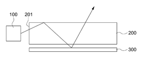
도 1은 본 발명의 실시예에 따른 백라이트 유닛의 개략도이고,
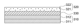
도 2는 본 발명의 실시예에 따른 광학시트의 단면도이고,
도 3은 본 발명의 실시예에 따른 광학시트의 변형예이고,
도 4는 본 발명의 또 다른 실시예에 따른 백라이트 유닛의 개략도이다.1 is a schematic diagram of a backlight unit according to an embodiment of the present invention,
2 is a cross-sectional view of an optical sheet according to an embodiment of the present invention,
3 is a modification of the optical sheet according to the embodiment of the present invention,
4 is a schematic view of a backlight unit according to another embodiment of the present invention.
본 발명은 다양한 변경을 가할 수 있고 여러 가지 실시예를 가질 수 있는 바, 특정 실시예들을 도면에 예시하고 상세한 설명에 상세하게 설명하고자 한다.As the invention allows for various changes and numerous embodiments, particular embodiments will be illustrated in the drawings and described in detail in the written description.
그러나, 이는 본 발명을 특정한 실시 형태에 대해 한정하려는 것이 아니며, 본 발명의 사상 및 기술 범위에 포함되는 모든 변경, 균등물 내지 대체물을 포함하는 것으로 이해되어야 한다.However, this is not intended to limit the present invention to specific embodiments, it should be understood to include all modifications, equivalents, and substitutes included in the spirit and scope of the present invention.
본 출원에서 사용한 용어는 단지 특정한 실시예를 설명하기 위해 사용된 것으로, 본 발명을 한정하려는 의도가 아니다. 단수의 표현은 문맥상 명백하게 다르게 뜻하지 않는 한, 복수의 표현을 포함한다.The terminology used herein is for the purpose of describing particular example embodiments only and is not intended to be limiting of the present invention. Singular expressions include plural expressions unless the context clearly indicates otherwise.
본 출원에서, "포함한다" 또는 "가지다" 등의 용어는 명세서상에 기재된 특징, 숫자, 단계, 동작, 구성요소, 부품 또는 이들을 조합한 것이 존재함을 지정하려는 것이지, 하나 또는 그 이상의 다른 특징들이나 숫자, 단계, 동작, 구성요소, 부품 또는 이들을 조합한 것들의 존재 또는 부가 가능성을 미리 배제하지 않는 것으로 이해되어야 한다.In the present application, the terms "comprises", "having", and the like are used to specify that a feature, a number, a step, an operation, an element, a component, But do not preclude the presence or addition of one or more other features, integers, steps, operations, elements, components, or combinations thereof.
또한 본 출원에서 첨부된 도면은 설명의 편의를 위하여 확대 또는 축소하여 도시된 것으로 이해되어야 한다.In addition, it is to be understood that the accompanying drawings in this application are shown enlarged or reduced for convenience of description.
이제 본 발명에 대하여 도면을 참고하여 상세하게 설명하고, 도면 부호에 관계없이 동일하거나 대응하는 구성 요소는 동일한 참조 번호를 부여하고 이에 대한 중복되는 설명은 생략하기로 한다.DETAILED DESCRIPTION OF THE PREFERRED EMBODIMENTS The present invention will now be described in detail with reference to the drawings. Like reference numerals designate like elements throughout, and duplicate descriptions thereof will be omitted.
도 1은 본 발명의 실시예에 따른 백라이트 유닛의 개략도이고, 도 2는 본 발명의 실시예에 따른 광학시트의 단면도이고, 도 3은 본 발명의 실시예에 따른 광학시트의 변형예이다.1 is a schematic view of a backlight unit according to an embodiment of the present invention, Figure 2 is a cross-sectional view of an optical sheet according to an embodiment of the present invention, Figure 3 is a modification of the optical sheet according to an embodiment of the present invention.
본 발명의 실시예에 따른 백라이트 유닛은 입광면(201)을 갖는 도광판(200)과, 상기 도광판(200)의 입광면에 배열되는 발광소자(100), 및 상기 도광판(200)의 하부에 형성되는 광학시트(300)를 포함한다.The backlight unit according to the embodiment of the present invention is formed on the
상기 도광판(200)은 상기 발광소자(100)에서 입사되는 점광원을 면광원으로 변환하는 광학 시트로서, 일반적인 도광판(200) 형상뿐만 아니라 실시예에 맞게 다양하게 변화할 수 있다. 예를 들면 모서리 부분에 직선면, 곡면 등과 같은 임의의 적합한 표면 형태가 적용될 수 있다.The
또한, 도면에는 도시되지 않았으나 도광판(200) 상면에 프리즘 형상의 요철이 형성될 수 있으며, 이러한 프리즘 형상의 요철은 직선면, 굴절면, 곡면 등과 같은 임의의 표면 형태로 이루어질 수도 있다.In addition, although not shown in the drawings, the prism-shaped unevenness may be formed on the upper surface of the
상기 발광소자(100)는 상기 도광판(200)의 입광면을 따라 복수 개가 형성되며, LED 소자로 형성될 수 있다. 이때 상기 발광소자(100)는 단파장의 광이 방출될 수 있는 백색 LED 또는 UV LED로 구성될 수 있다.The
상기 광학시트(300)는 도광판(200)의 하부로 방출된 광을 반사시켜 다시 도광판(200)으로 재입사시키는 역할을 수행한다. 따라서 광을 반사시키기 가장 적합한 재료 및 구성이 다양하게 선택될 수 있다.The
본 발명에 따른 광학시트(300)는 크게 반사층(310)과 파장변환층(320)으로 구성되는데, 먼저 반사층(310)은 일반적인 디스플레이용 반사판의 구성이 모두 적용될 수 있다. The
예를 들면, 은(Ag), 알루미늄(Al)과 같은 금속 박막을 이용할 수도 있고, 필름과 같은 베이스 기재(311)상에 은(Ag)과 같은 금속 페이스트(312)를 소정의 두께로 도포한 뒤 경화시켜 제조할 수 있다. 또는 베이스 기재(311) 상에 금속 입자를 스퍼터링 또는 스크린 코팅하여 금속층을 형성할 수도 있다. For example, a metal thin film such as silver (Ag) or aluminum (Al) may be used, and a
상기 파장변환층(320)은 고분자 수지(321)에 양자점(322)이 분산되어 형성된다. 양자점(Quantum Dots: QDs)이란 양자고립효과(quantum confinement effect)를 가지는 소정크기의 나노 입자로서, 양자점의 발광파장보다 작은 파장을 갖는 광(여기광)을 흡수하여 좁은 파장대에서 강한 형광을 발생한다.The
이러한 양자점(322)으로는 ZnS, ZnSe, ZnTe, CdS CdSe와 같은 II-VI족계 화합물 반도체, PbS, PbSe, PbTe, AlN, AlP, AlAs와 같은 III-V족계 화합물 반도체, IV-VI족계 화합물 반도체 또는 이들의 혼합물로 이루어진 군에서 어느 하나가 선택될 수 있다. Such
양자점의 제조방법은 일반적으로 사용되는 제조방법 모두 적용될 수 있다. 예를 들면, CdSe 양자점의 경우 Cd 전구체와 Se 전구체를 각각 용해시킨 후, Se 전구체 용액을 Cd 전구체를 녹인 용액에 천천히 주입하고 약 20시간 정도 교반하여 CdSe 양자점 코어(core)를 제조할 수 있다. 이후 동일한 방법으로 ZnS 전구체를 코어 주변에 성장시킴으로써 코어-쉘 구조의 양자점을 제작할 수 있다.The manufacturing method of the quantum dot can be applied to all the manufacturing methods commonly used. For example, in the case of CdSe quantum dots, after dissolving the Cd precursor and Se precursor, respectively, the Se precursor solution may be slowly injected into the solution in which the Cd precursor is dissolved and stirred for about 20 hours to prepare a CdSe quantum dot core. Subsequently, a ZnS precursor may be grown around the core in the same manner to prepare a quantum dot of a core-shell structure.
이때 원하는 발광파장을 갖도록 양자점의 크기를 제어할 수도 있다. 양자점의 크기를 제어하는 방법 역시 공지의 다양한 방법이 적용될 수 있다. 예를 들면, 콜로이드법으로 코어를 온도조건 및 시간에 따라 성장시켜 양자점의 코어 사이즈를 달리 제작할 수 있다.In this case, the size of the quantum dot may be controlled to have a desired emission wavelength. A method for controlling the size of a quantum dot may also be applied to various known methods. For example, the cores may be grown according to temperature conditions and time by a colloidal method to produce different core sizes of quantum dots.
양자점(322)의 분산매질인 고분자 수지(321)는 에폭시 수지 또는 실리콘과 같이 여기광 등에 의하여 변색되거나 변질되지 않는 내광성, 또는 내습성 강한 재질인 것이 바람직하다. 파장변환층(320)은 액체 상태의 고분자 수지(321)와 양자점(322)을 혼합한 뒤 경화되기 전 롤링(rolling) 등 공지의 방법에 의하여 시트 형태로 성형할 수 있다.The
양자점(322)이 혼합된 고분자 수지(321)를 시트 형태로 성형하고 경화시켜 반사층(310) 상에 대면적이면서 균일한 농도의 양자점(322)을 포함하는 파장변환층(320)을 형성할 수 있다.The
본 발명에서는 도광판(200)에서 광학시트(300)로 입사되는 여기광(자외선 영역 포함)이 파장변환층(320)을 통과하면서 블루 파장대(380nm 내지 480nm)의 광으로 변환되도록 제어된다. 즉, 도 2와 같이 양자점(322)은 380nm이하의 파장대를 갖는 여기광(P1)을 흡수한 후 380nm 내지 480nm의 파장대를 갖는 광(P2)을 방출하는 것이다.In the present invention, the excitation light (including the ultraviolet region) incident on the
양자점은 코어의 사이즈가 작아질수록 발광파장이 작아지므로 480nm 이하의 발광파장을 갖기 위하여는 양자점(322)의 코어가 약 5nm이하의 사이즈를 갖는 것이 바람직하다.Since the light emission wavelength is smaller as the size of the quantum dot is smaller, it is preferable that the core of the
그 결과 반사층(310)과 파장변환층(320)과의 계면에서 발생하는 표면 플라즈몬 공명 현상(Surface Plasmon Resonance, SPR)에 의하여 450nm이하의 파장대를 갖는 광의 반사율이 감소하여도, 380nm 내지 480nm의 파장대를 갖는 광의 광량이 증가하므로 블루 영역 파장대에서의 반사율 하락을 보상할 수 있게 된다. 또한 종래 반사판에 의해 반사되지 않는 단파장의 광을 활용하므로 전체적인 광량이 증가하여 휘도가 높아지는 장점이 있다.As a result, even if the reflectance of light having a wavelength band of 450 nm or less is reduced by Surface Plasmon Resonance (SPR) occurring at the interface between the
이때 양자점(322)의 중량비가 고분자 수지 대비 1wt% 미만인 경우에는 표면 플라즈몬 공명 현상(Surface Plasmon Resonance, SPR)을 보상할 정도로 충분히 블루 파장대의 광량을 증가시킬 수 없는 문제가 있고, 고분자 수지 대비 3wt%를 초과하는 경우에는 자기 소멸 현상(self quenching)으로 인하여 발광되는 광을 근접한 양자점이 다시 재흡수 하는 현상이 발생하여 발광 효율이 크게 하락하는 문제가 있다. 따라서 고분자 수지와 양자점의 중량비(wt%)는 99:1 내지 97:3인 것이 바람직하다.In this case, when the weight ratio of the
또한, 파장변환층(320)의 두께가 100nm 미만일 경우, 광학시트에서 반사되어 나오는 광의 손실이 적으나 SPR 효과가 상대적으로 커져서 블루 파장대역의 광손실이 더 큰 문제가 있고, 두께가 10㎛이상인 경우에는 SPR에 의한 감소 효과는 적으나, 두꺼운 두께로 인하여 도광판으로 재입사되는 광량이 상대적으로 적어지고, 파장변환층의 막 박리 현상이 발생하는 문제가 있다. 따라서 파장변환층(320)의 두께는 100nm 이상 10㎛ 이하인 것이 바람직하다.In addition, when the thickness of the
본 발명에 따르면 파장변환층(320)에 의하여 반사층(310)의 금속이 산화되는 것을 방지하는 동시에 양자점(322)에 의하여 380nm 내지 480nm의 파장대를 갖는 광량을 증가시켜 도광판(200)으로 재입사되는 전체 광의 RGB의 값이 균일해지도록 제어할 수 있다.According to the present invention, the metal of the
그러나 상기 광학시트(300)의 구성은 반드시 이에 한정되는 것은 아니고 다양한 변형이 가능하다. 예를 들면, 도 3과 같이 반사층(310) 상에 별도의 보호층(330)이 형성되고 그 위에 파장변환층(320)이 형성될 수도 있는 것이다.However, the configuration of the
이하에서는 410nm, 450nm의 중심 발광파장대를 갖는 양자점을 고분자 수지에 혼합한 후, 반사층 상에 코팅한 광학시트(실시예 1, 실시예 2) 및 보호코팅한 은(Ag) 반사판(비교예 1)에 대해 각각 휘도 및 색좌표를 측정하여 표 1에 기재하였다.Hereinafter, after mixing the quantum dots having a central emission wavelength band of 410nm, 450nm to the polymer resin, and then coated on the reflective layer (Example 1, Example 2) and the protective coating silver (Ag) reflector (Comparative Example 1) The luminance and color coordinates were measured for each, and are shown in Table 1 below.
상기 표 1을 참조하면, 실시예 1과 2의 경우 모두 비교예 1과 비교하여 휘도가 증가한 것을 알 수 있으며, 색좌표 값은 X축과 Y축의 값이 백색광 영역의 좌표와 근접해져 비교예 1에 비해 백색광에 더 가까워졌음을 알 수 있다.
Referring to Table 1, it can be seen that in the case of Examples 1 and 2, the brightness is increased in comparison with Comparative Example 1, the color coordinate value of the X-axis and Y-axis is close to the coordinates of the white light region in Comparative Example 1 It can be seen that closer to white light.
도 4는 본 발명의 또 다른 실시예에 따른 백라이트 유닛의 개략도이다. 이를 참조할 때 본 발명에 따른 백라이트 유닛은 도광판(200)의 하부에 파장변환층(320)이 형성될 수 있다.4 is a schematic diagram of a backlight unit according to another exemplary embodiment of the present invention. Referring to this, in the backlight unit according to the present invention, the
이때 파장변환층(320)은 코팅 등의 방법에 의해 도광판(200)의 하부에 일체로 형성될 수도 있으며, 광학시트(300)의 반사층(310) 상에 형성되어 도광판(200)에 부착될 수도 있다. 파장변환층(320)이 도광판(200)의 하부에 형성된 경우 광학시트(300)는 일반적인 반사판의 구성을 가질 수 있다.In this case, the
이러한 구성에 의하여 최초 도광판(200)의 입사면을 통과하여 내부로 입사된 광 중 일부는 파장변환층(320) 방향으로 입사된다.By this configuration, some of the light incident through the incident surface of the
이때, 파장변환층(320)이 도광판(200)보다 굴절률이 높게 형성된 경우에는 전반사 임계각보다 큰 각도로 굴절된 광은 도광판(200)과의 경계면에 반사되므로 파장변환층(320) 내에서 연속적으로 반사되다가 전반사 임계각보다 작은 각도로 굴절/산란될 때 도광판(200)으로 입사된다.In this case, when the
또한, 상기 파장변환층(320)이 도광판(200)에 비하여 상대적으로 얇게 형성된 경우, 광은 도광판(200)과의 경계면과 반사층(310)과의 경계면 사이에서 굴절/산란/반사가 반복되는 회수가 증가하기 때문에 파장변환층(320) 내부에서 흡수되기 전에 전반사 각도보다 작은 각으로 방출될 확률이 높아지게 되어 도광판(200) 내부에서 광이 흡수되는 문제를 해결할 수 있다.In addition, when the
본 발명에서는 백라이트 유닛을 포함하는 액정표시장치를 포함하나, 액정표시장치의 구성은 공지의 구성이 모두 적용될 수 있는바 자세한 설명은 생략한다.
The present invention includes a liquid crystal display device including a backlight unit, but the configuration of the liquid crystal display device may be applied to all known configurations, and thus a detailed description thereof will be omitted.
상술한 바와 같이, 본 발명은 바람직한 실시예를 통하여 상세히 설명되었지만, 본 발명은 이러한 실시예의 내용에 제한되는 것은 아니다. 본 발명이 속하는 기술분야에서 통상의 지식을 가진 자라면, 비록 실시예에 개시되지 않았지만 첨부된 청구항의 기재범위 내에서 다양한 수정, 변경 또는 부가가 가능하며, 이들 모두 본 발명의 기술적 범위에 속하는 것으로 보아야 할 것이다. As described above, the present invention has been described in detail through the preferred embodiments, but the present invention is not limited to the contents of these embodiments. Those skilled in the art to which the present invention pertains, although not disclosed in the embodiments, various modifications, changes or additions are possible within the scope of the appended claims, all of which fall within the technical scope of the present invention. You will have to look.
100: 발광소자 200: 도광판
300: 광학시트 310: 반사층
320: 파장변환층 321: 고분자 수지
322: 양자점100: light emitting device 200: light guide plate
300: optical sheet 310: reflective layer
320: wavelength conversion layer 321: polymer resin
322: quantum dots
Claims (13)
상기 반사층 상에 형성되는 파장변환층;을 포함하되,
상기 파장변환층은 고분자 수지에 양자점이 분산되어 형성된 광학시트.Reflective layer; And
Including; a wavelength conversion layer formed on the reflective layer,
The wavelength conversion layer is an optical sheet formed by dispersing quantum dots in a polymer resin.
상기 도광판의 입광면에 배열되는 발광소자; 및
상기 도광판의 하부에 형성되는 광학시트를 포함하되,
상기 광학시트는 반사층, 및 상기 반사층의 상부에 형성되는 파장변환층을 포함하고, 상기 파장변환층은 고분자 수지에 양자점이 분산되어 형성된 백라이트 유닛.A light guide plate having a light incident surface;
A light emitting element arranged on a light incident surface of the light guide plate; And
Including an optical sheet formed under the light guide plate,
The optical sheet includes a reflective layer and a wavelength conversion layer formed on the reflective layer, wherein the wavelength conversion layer is formed by dispersing quantum dots in a polymer resin.
상기 도광판의 입광면에 배열되는 발광소자; 및
상기 도광판의 하부에 형성되는 광학시트를 포함하되,
상기 도광판의 하부에는 파장변환층이 형성되고, 상기 파장변환층은 고분자 수지에 양자점이 분산되어 형성된 백라이트 유닛.A light guide plate having a light incident surface;
A light emitting element arranged on a light incident surface of the light guide plate; And
Including an optical sheet formed under the light guide plate,
A wavelength conversion layer is formed below the light guide plate, and the wavelength conversion layer is formed by dispersing quantum dots in a polymer resin.
Priority Applications (1)
| Application Number | Priority Date | Filing Date | Title |
|---|---|---|---|
| KR1020110011812A KR101114412B1 (en) | 2011-02-10 | 2011-02-10 | Optical sheet in which nano quantum dots are dispersed and backlight unit including the same |
Applications Claiming Priority (1)
| Application Number | Priority Date | Filing Date | Title |
|---|---|---|---|
| KR1020110011812A KR101114412B1 (en) | 2011-02-10 | 2011-02-10 | Optical sheet in which nano quantum dots are dispersed and backlight unit including the same |
Publications (1)
| Publication Number | Publication Date |
|---|---|
| KR101114412B1 true KR101114412B1 (en) | 2012-02-22 |
Family
ID=45840373
Family Applications (1)
| Application Number | Title | Priority Date | Filing Date |
|---|---|---|---|
| KR1020110011812A Active KR101114412B1 (en) | 2011-02-10 | 2011-02-10 | Optical sheet in which nano quantum dots are dispersed and backlight unit including the same |
Country Status (1)
| Country | Link |
|---|---|
| KR (1) | KR101114412B1 (en) |
Cited By (7)
| Publication number | Priority date | Publication date | Assignee | Title |
|---|---|---|---|---|
| KR101360638B1 (en) * | 2012-04-27 | 2014-02-10 | 엘지이노텍 주식회사 | Display, light conversion member and method of fabricating light conversion member |
| WO2014073894A1 (en) * | 2012-11-09 | 2014-05-15 | 주식회사 엘엠에스 | Optical sheet and backlight unit comprising same |
| KR101503290B1 (en) | 2012-11-09 | 2015-03-18 | 주식회사 엘엠에스 | Optical sheet and backlight unit having the optical sheet |
| CN105845028A (en) * | 2016-05-19 | 2016-08-10 | 信利(惠州)智能显示有限公司 | Application of transparent conductive film and silver nanowires in display |
| US9650567B2 (en) | 2013-12-20 | 2017-05-16 | Samsung Display Co., Ltd. | Wavelength converter and liquid crystal display including the same |
| US9765937B2 (en) | 2013-09-13 | 2017-09-19 | Samsung Display Co., Ltd. | Light source, a method of manufacturing the same, and a backlight unit having the same |
| CN110738940A (en) * | 2019-11-28 | 2020-01-31 | 京东方科技集团股份有限公司 | Quantum dot film, color film layer and display device |
Citations (3)
| Publication number | Priority date | Publication date | Assignee | Title |
|---|---|---|---|---|
| KR20100029519A (en) * | 2008-09-08 | 2010-03-17 | 삼성전기주식회사 | Quantum dot-wavelength conversion sheet, preparing method of the same and light-emitting device comprising the same |
| KR20100047841A (en) * | 2007-07-18 | 2010-05-10 | 큐디 비젼, 인크. | Quantum dot-based light sheets useful for solid-state lighting |
| KR20100129030A (en) * | 2009-05-29 | 2010-12-08 | 삼성엘이디 주식회사 | Wavelength conversion sheet and light emitting device using the same |
-
2011
- 2011-02-10 KR KR1020110011812A patent/KR101114412B1/en active Active
Patent Citations (3)
| Publication number | Priority date | Publication date | Assignee | Title |
|---|---|---|---|---|
| KR20100047841A (en) * | 2007-07-18 | 2010-05-10 | 큐디 비젼, 인크. | Quantum dot-based light sheets useful for solid-state lighting |
| KR20100029519A (en) * | 2008-09-08 | 2010-03-17 | 삼성전기주식회사 | Quantum dot-wavelength conversion sheet, preparing method of the same and light-emitting device comprising the same |
| KR20100129030A (en) * | 2009-05-29 | 2010-12-08 | 삼성엘이디 주식회사 | Wavelength conversion sheet and light emitting device using the same |
Cited By (7)
| Publication number | Priority date | Publication date | Assignee | Title |
|---|---|---|---|---|
| KR101360638B1 (en) * | 2012-04-27 | 2014-02-10 | 엘지이노텍 주식회사 | Display, light conversion member and method of fabricating light conversion member |
| WO2014073894A1 (en) * | 2012-11-09 | 2014-05-15 | 주식회사 엘엠에스 | Optical sheet and backlight unit comprising same |
| KR101503290B1 (en) | 2012-11-09 | 2015-03-18 | 주식회사 엘엠에스 | Optical sheet and backlight unit having the optical sheet |
| US9765937B2 (en) | 2013-09-13 | 2017-09-19 | Samsung Display Co., Ltd. | Light source, a method of manufacturing the same, and a backlight unit having the same |
| US9650567B2 (en) | 2013-12-20 | 2017-05-16 | Samsung Display Co., Ltd. | Wavelength converter and liquid crystal display including the same |
| CN105845028A (en) * | 2016-05-19 | 2016-08-10 | 信利(惠州)智能显示有限公司 | Application of transparent conductive film and silver nanowires in display |
| CN110738940A (en) * | 2019-11-28 | 2020-01-31 | 京东方科技集团股份有限公司 | Quantum dot film, color film layer and display device |
Similar Documents
| Publication | Publication Date | Title |
|---|---|---|
| KR101114412B1 (en) | Optical sheet in which nano quantum dots are dispersed and backlight unit including the same | |
| KR101730164B1 (en) | Quantum dot-based light sheets useful for solid-state lighting | |
| KR101604339B1 (en) | Light conversion film, baclight unit and display devive comprising the same | |
| JP5654676B2 (en) | Display device | |
| TWI631395B (en) | Optical member, display device having the same and method of fabricating the same | |
| TWI498642B (en) | Optical member, display device having the same and method for fabricating the same | |
| TWI731394B (en) | Light-emitting device | |
| EP2214218A2 (en) | Light emitting diode unit, display apparatus having the same and manufacturing method of the same | |
| KR101775260B1 (en) | Fluorescent films having adjustable color location and color gamut | |
| CN107424524B (en) | Miniature LED display panel | |
| KR101745599B1 (en) | Quantum dot optical sheet and method for preparing same | |
| US20060072339A1 (en) | Backlight module | |
| CN107121841B (en) | It is a kind of for the light conversion film of backlight module, backlight module and display equipment | |
| JP2010533976A5 (en) | ||
| CN111808603A (en) | A kind of quantum dot film and its preparation method, display device | |
| CN108873465A (en) | Quantum dot display base plate and preparation method thereof, display device | |
| AU2017350734A1 (en) | Backlight unit for a display device | |
| JP2024037888A (en) | display device | |
| WO2018201617A1 (en) | Optical film assembly, backlight module, and display apparatus | |
| US11209697B1 (en) | Backlight unit with phosphors and quantum dots | |
| KR102054274B1 (en) | Quantum dot optical sheet, back light unit comprising the same and display apparatus | |
| JP2018055029A (en) | Quantum dot sheet, backlight and liquid crystal display device | |
| CN110989296A (en) | Quantum dot photoresist and preparation method thereof, display substrate and display device | |
| CN115218160A (en) | Backlight module | |
| CN110028949A (en) | The compound membrane preparation method of quantum dot, backlight module |
Legal Events
| Date | Code | Title | Description |
|---|---|---|---|
| A201 | Request for examination | ||
| PA0109 | Patent application |
St.27 status event code: A-0-1-A10-A12-nap-PA0109 |
|
| PA0201 | Request for examination |
St.27 status event code: A-1-2-D10-D11-exm-PA0201 |
|
| R18-X000 | Changes to party contact information recorded |
St.27 status event code: A-3-3-R10-R18-oth-X000 |
|
| R18-X000 | Changes to party contact information recorded |
St.27 status event code: A-3-3-R10-R18-oth-X000 |
|
| D13-X000 | Search requested |
St.27 status event code: A-1-2-D10-D13-srh-X000 |
|
| D14-X000 | Search report completed |
St.27 status event code: A-1-2-D10-D14-srh-X000 |
|
| E701 | Decision to grant or registration of patent right | ||
| PE0701 | Decision of registration |
St.27 status event code: A-1-2-D10-D22-exm-PE0701 |
|
| GRNT | Written decision to grant | ||
| PR0701 | Registration of establishment |
St.27 status event code: A-2-4-F10-F11-exm-PR0701 |
|
| PR1002 | Payment of registration fee |
St.27 status event code: A-2-2-U10-U11-oth-PR1002 Fee payment year number: 1 |
|
| PG1601 | Publication of registration |
St.27 status event code: A-4-4-Q10-Q13-nap-PG1601 |
|
| FPAY | Annual fee payment |
Payment date: 20150202 Year of fee payment: 4 |
|
| PR1001 | Payment of annual fee |
St.27 status event code: A-4-4-U10-U11-oth-PR1001 Fee payment year number: 4 |
|
| FPAY | Annual fee payment |
Payment date: 20160203 Year of fee payment: 5 |
|
| PR1001 | Payment of annual fee |
St.27 status event code: A-4-4-U10-U11-oth-PR1001 Fee payment year number: 5 |
|
| P22-X000 | Classification modified |
St.27 status event code: A-4-4-P10-P22-nap-X000 |
|
| FPAY | Annual fee payment |
Payment date: 20170203 Year of fee payment: 6 |
|
| PR1001 | Payment of annual fee |
St.27 status event code: A-4-4-U10-U11-oth-PR1001 Fee payment year number: 6 |
|
| FPAY | Annual fee payment |
Payment date: 20180202 Year of fee payment: 7 |
|
| PR1001 | Payment of annual fee |
St.27 status event code: A-4-4-U10-U11-oth-PR1001 Fee payment year number: 7 |
|
| FPAY | Annual fee payment |
Payment date: 20190201 Year of fee payment: 8 |
|
| PR1001 | Payment of annual fee |
St.27 status event code: A-4-4-U10-U11-oth-PR1001 Fee payment year number: 8 |
|
| PR1001 | Payment of annual fee |
St.27 status event code: A-4-4-U10-U11-oth-PR1001 Fee payment year number: 9 |
|
| PR1001 | Payment of annual fee |
St.27 status event code: A-4-4-U10-U11-oth-PR1001 Fee payment year number: 10 |
|
| PR1001 | Payment of annual fee |
St.27 status event code: A-4-4-U10-U11-oth-PR1001 Fee payment year number: 11 |
|
| PR1001 | Payment of annual fee |
St.27 status event code: A-4-4-U10-U11-oth-PR1001 Fee payment year number: 12 |
|
| PR1001 | Payment of annual fee |
St.27 status event code: A-4-4-U10-U11-oth-PR1001 Fee payment year number: 13 |
|
| PR1001 | Payment of annual fee |
St.27 status event code: A-4-4-U10-U11-oth-PR1001 Fee payment year number: 14 |
|
| PR1001 | Payment of annual fee |
St.27 status event code: A-4-4-U10-U11-oth-PR1001 Fee payment year number: 15 |
|
| U11 | Full renewal or maintenance fee paid |
Free format text: ST27 STATUS EVENT CODE: A-4-4-U10-U11-OTH-PR1001 (AS PROVIDED BY THE NATIONAL OFFICE) Year of fee payment: 15 |