KR101017848B1 - Beam homogenizer and laser irradiation device and semiconductor device manufacturing method - Google Patents
Beam homogenizer and laser irradiation device and semiconductor device manufacturing method Download PDFInfo
- Publication number
- KR101017848B1 KR101017848B1 KR1020030065026A KR20030065026A KR101017848B1 KR 101017848 B1 KR101017848 B1 KR 101017848B1 KR 1020030065026 A KR1020030065026 A KR 1020030065026A KR 20030065026 A KR20030065026 A KR 20030065026A KR 101017848 B1 KR101017848 B1 KR 101017848B1
- Authority
- KR
- South Korea
- Prior art keywords
- laser
- laser light
- width direction
- linear
- semiconductor film
- Prior art date
- Legal status (The legal status is an assumption and is not a legal conclusion. Google has not performed a legal analysis and makes no representation as to the accuracy of the status listed.)
- Expired - Fee Related
Links
Images




Classifications
-
- G—PHYSICS
- G02—OPTICS
- G02B—OPTICAL ELEMENTS, SYSTEMS OR APPARATUS
- G02B27/00—Optical systems or apparatus not provided for by any of the groups G02B1/00 - G02B26/00, G02B30/00
- G02B27/09—Beam shaping, e.g. changing the cross-sectional area, not otherwise provided for
- G02B27/0927—Systems for changing the beam intensity distribution, e.g. Gaussian to top-hat
-
- H—ELECTRICITY
- H10—SEMICONDUCTOR DEVICES; ELECTRIC SOLID-STATE DEVICES NOT OTHERWISE PROVIDED FOR
- H10P—GENERIC PROCESSES OR APPARATUS FOR THE MANUFACTURE OR TREATMENT OF DEVICES COVERED BY CLASS H10
- H10P95/00—Generic processes or apparatus for manufacture or treatments not covered by the other groups of this subclass
- H10P95/90—Thermal treatments, e.g. annealing or sintering
-
- B—PERFORMING OPERATIONS; TRANSPORTING
- B23—MACHINE TOOLS; METAL-WORKING NOT OTHERWISE PROVIDED FOR
- B23K—SOLDERING OR UNSOLDERING; WELDING; CLADDING OR PLATING BY SOLDERING OR WELDING; CUTTING BY APPLYING HEAT LOCALLY, e.g. FLAME CUTTING; WORKING BY LASER BEAM
- B23K26/00—Working by laser beam, e.g. welding, cutting or boring
- B23K26/02—Positioning or observing the workpiece, e.g. with respect to the point of impact; Aligning, aiming or focusing the laser beam
- B23K26/06—Shaping the laser beam, e.g. by masks or multi-focusing
- B23K26/064—Shaping the laser beam, e.g. by masks or multi-focusing by means of optical elements, e.g. lenses, mirrors or prisms
-
- B—PERFORMING OPERATIONS; TRANSPORTING
- B23—MACHINE TOOLS; METAL-WORKING NOT OTHERWISE PROVIDED FOR
- B23K—SOLDERING OR UNSOLDERING; WELDING; CLADDING OR PLATING BY SOLDERING OR WELDING; CUTTING BY APPLYING HEAT LOCALLY, e.g. FLAME CUTTING; WORKING BY LASER BEAM
- B23K26/00—Working by laser beam, e.g. welding, cutting or boring
- B23K26/02—Positioning or observing the workpiece, e.g. with respect to the point of impact; Aligning, aiming or focusing the laser beam
- B23K26/06—Shaping the laser beam, e.g. by masks or multi-focusing
- B23K26/064—Shaping the laser beam, e.g. by masks or multi-focusing by means of optical elements, e.g. lenses, mirrors or prisms
- B23K26/0648—Shaping the laser beam, e.g. by masks or multi-focusing by means of optical elements, e.g. lenses, mirrors or prisms comprising lenses
-
- B—PERFORMING OPERATIONS; TRANSPORTING
- B23—MACHINE TOOLS; METAL-WORKING NOT OTHERWISE PROVIDED FOR
- B23K—SOLDERING OR UNSOLDERING; WELDING; CLADDING OR PLATING BY SOLDERING OR WELDING; CUTTING BY APPLYING HEAT LOCALLY, e.g. FLAME CUTTING; WORKING BY LASER BEAM
- B23K26/00—Working by laser beam, e.g. welding, cutting or boring
- B23K26/02—Positioning or observing the workpiece, e.g. with respect to the point of impact; Aligning, aiming or focusing the laser beam
- B23K26/06—Shaping the laser beam, e.g. by masks or multi-focusing
- B23K26/073—Shaping the laser spot
- B23K26/0732—Shaping the laser spot into a rectangular shape
-
- B—PERFORMING OPERATIONS; TRANSPORTING
- B23—MACHINE TOOLS; METAL-WORKING NOT OTHERWISE PROVIDED FOR
- B23K—SOLDERING OR UNSOLDERING; WELDING; CLADDING OR PLATING BY SOLDERING OR WELDING; CUTTING BY APPLYING HEAT LOCALLY, e.g. FLAME CUTTING; WORKING BY LASER BEAM
- B23K26/00—Working by laser beam, e.g. welding, cutting or boring
- B23K26/02—Positioning or observing the workpiece, e.g. with respect to the point of impact; Aligning, aiming or focusing the laser beam
- B23K26/06—Shaping the laser beam, e.g. by masks or multi-focusing
- B23K26/073—Shaping the laser spot
- B23K26/0738—Shaping the laser spot into a linear shape
-
- G—PHYSICS
- G02—OPTICS
- G02B—OPTICAL ELEMENTS, SYSTEMS OR APPARATUS
- G02B27/00—Optical systems or apparatus not provided for by any of the groups G02B1/00 - G02B26/00, G02B30/00
- G02B27/09—Beam shaping, e.g. changing the cross-sectional area, not otherwise provided for
-
- G—PHYSICS
- G02—OPTICS
- G02B—OPTICAL ELEMENTS, SYSTEMS OR APPARATUS
- G02B27/00—Optical systems or apparatus not provided for by any of the groups G02B1/00 - G02B26/00, G02B30/00
- G02B27/09—Beam shaping, e.g. changing the cross-sectional area, not otherwise provided for
- G02B27/0938—Using specific optical elements
- G02B27/0994—Fibers, light pipes
-
- Y—GENERAL TAGGING OF NEW TECHNOLOGICAL DEVELOPMENTS; GENERAL TAGGING OF CROSS-SECTIONAL TECHNOLOGIES SPANNING OVER SEVERAL SECTIONS OF THE IPC; TECHNICAL SUBJECTS COVERED BY FORMER USPC CROSS-REFERENCE ART COLLECTIONS [XRACs] AND DIGESTS
- Y10—TECHNICAL SUBJECTS COVERED BY FORMER USPC
- Y10T—TECHNICAL SUBJECTS COVERED BY FORMER US CLASSIFICATION
- Y10T117/00—Single-crystal, oriented-crystal, and epitaxy growth processes; non-coating apparatus therefor
- Y10T117/10—Apparatus
- Y10T117/1004—Apparatus with means for measuring, testing, or sensing
- Y10T117/1008—Apparatus with means for measuring, testing, or sensing with responsive control means
Landscapes
- Physics & Mathematics (AREA)
- Optics & Photonics (AREA)
- Engineering & Computer Science (AREA)
- Plasma & Fusion (AREA)
- Mechanical Engineering (AREA)
- General Physics & Mathematics (AREA)
- Recrystallisation Techniques (AREA)
Abstract
피조사면 상의 빔 스폿에서의 불균일한 에너지 분포는 광학 시스템을 형성하는 원통형 렌즈 어레이의 구조적인 문제점 및 가공 정밀도에 의해 야기된다.Uneven energy distribution at the beam spot on the irradiated surface is caused by structural problems and processing precision of the cylindrical lens array forming the optical system.
본 발명에 따르면, 직사각형 빔 스폿을 형성하기 위한 광학 시스템에 있어서, 피조사면 상의 레이저광의 직사각형 빔 스폿의 짧은 변 방향의 에너지 분포를 균일화하기 위한 광학 시스템은 광도파로로 대체된다. 상기 광도파로는 방사빔을 일정 영역에 한정하고 그 에너지 흐름을 경로의 축에 평행하게 전송할 수 있는 회로이다.According to the present invention, in the optical system for forming the rectangular beam spot, the optical system for equalizing the energy distribution in the short side direction of the rectangular beam spot of the laser light on the irradiated surface is replaced with an optical waveguide. The optical waveguide is a circuit capable of confining a radiation beam to a certain area and transmitting its energy flow parallel to the axis of the path.
직사각형 빔 스폿, 에너지 분포, 광학 시스템, 원통형 렌즈 어레이, 레이저광, 광도파로Rectangular beam spot, energy distribution, optical system, cylindrical lens array, laser light, optical waveguide
Description
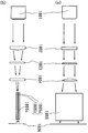
도 1은 본 발명의 수단을 도시하는 도면.1 shows the means of the present invention;
도 2는 본 발명에 개시된 레이저 조사 장치의 예를 도시하는 도면.2 is a diagram showing an example of a laser irradiation apparatus disclosed in the present invention.
도 3은 도 2에 도시된 광학 시스템에 의해 처리된 직사각형 빔 스폿의 에너지 분포를 도시하는 도면.FIG. 3 shows the energy distribution of a rectangular beam spot processed by the optical system shown in FIG. 2. FIG.
도 4는 본 발명에 개시된 레이저 조사 장치의 예를 도시하는 도면.4 is a diagram showing an example of a laser irradiation apparatus disclosed in the present invention.
도 5는 도 4에 도시된 광학 시스템에 의해 처리된 직사각형 빔 스폿의 에너지 분포를 도시하는 도면.FIG. 5 shows the energy distribution of a rectangular beam spot processed by the optical system shown in FIG. 4. FIG.
도 6은 본 발명에 개시된 레이저 조사 장치의 예를 도시하는 도면.6 is a diagram showing an example of the laser irradiation apparatus disclosed in the present invention.
도 7은 도 6에 도시된 광학 시스템에 의해 처리된 직사각형 빔 스폿의 에너지 분포를 도시하는 도면.FIG. 7 shows the energy distribution of rectangular beam spots processed by the optical system shown in FIG. 6. FIG.
도 8은 본 발명에 개시된 레이저 조사 장치의 예를 도시하는 도면.8 is a diagram showing an example of a laser irradiation apparatus disclosed in the present invention.
도 9는 도 8에 도시된 광학 시스템에 의해 처리된 직사각형 빔 스폿의 에너지 분포를 도시하는 도면.FIG. 9 shows the energy distribution of a rectangular beam spot processed by the optical system shown in FIG. 8. FIG.
도 10은 종래의 레이저 조사 장치를 도시하는 도면. 10 shows a conventional laser irradiation apparatus;
* 도면의 주요 부분에 대한 부호의 설명 *Explanation of symbols on the main parts of the drawings
1101 : 레이저 발진기 1102a, 1102b : 구면 렌즈1101:
1103a, 1103b : 원통형 렌즈 어레이 1104, 1105 : 원통형 렌즈1103a, 1103b:
1106 : 광도파로 1106a, 1106b : 반사면1106:
1107a, 1107b : 2겹 원통형 렌즈 1108 : 피조사면1107a, 1107b: 2-ply cylindrical lens 1108: irradiated surface
본 발명은 피조사면 상에서의 빔 스폿을 특정 영역에서 균일화하는 빔 호모지나이저(beam homogenizer)에 관한 것이며, 또한 피조사면 상에 균일화된 빔 스폿을 조사하는 레이저 조사 장치에 관한 것이다. 본 발명에 따른 반도체 장치는, 액티브 매트릭스 액정표시장치 및 액티브 매트릭스 전자 발광 표시장치와 같은 표시장치와, 전기 광학 장치와, 상기 표시장치 또는 전기 광학 장치를 이용하는 전기 기기를 포함하고, 또한, 본 발명은 반도체 장치 제조 방법에 관한 것이다.The present invention relates to a beam homogenizer for uniformizing a beam spot on a surface to be irradiated in a specific area, and also to a laser irradiation apparatus for irradiating a beam spot uniform to a surface to be irradiated. The semiconductor device according to the present invention includes a display device such as an active matrix liquid crystal display device and an active matrix electroluminescent display device, an electro-optical device, and an electric device using the display device or the electro-optical device. Relates to a semiconductor device manufacturing method.
최근, 글래스 등의 절연 기판상에 형성된 비정질 반도체막 또는 결정성 반도체막(단결정이 아닌 다결정 또는 미세결정 등의 결정성을 갖는 반도체막)의 결정성을 결정화하거나 또는 향상시키는 레이저 어닐링 기술이 폭 넓게 연구되고 있다. 상기 반도체막은 일반적으로 규소 반도체막으로 형성된다.Recently, a laser annealing technique for crystallizing or improving the crystallinity of an amorphous semiconductor film or a crystalline semiconductor film (a semiconductor film having crystallinity such as polycrystal or microcrystal, not single crystal) formed on an insulating substrate such as glass has been widely used. Is being studied. The semiconductor film is generally formed of a silicon semiconductor film.
통상적으로 사용되고 있는 석영 기판과 비교하여, 글래스 기판은 보다 경제적이고, 높은 작업성을 가지며, 대면적을 구비하는 기판이 용이하게 제작될 수 있다는 이점을 갖는다. 이 때문에, 상기 연구가 광범위하게 수행되고 있다. 글래스 기판의 융점이 낮기 때문에, 레이저가 결정화를 위해 바람직하게 사용된다. 레이저는 기판의 온도를 크게 변화시킴이 없이 비-단결정(non-single-crystal) 반도체막에만 높은 에너지를 부여할 수 있다.Compared with the commonly used quartz substrate, the glass substrate has the advantage of being more economical, having a high workability, and a substrate having a large area can be easily manufactured. For this reason, the above research is extensively performed. Since the melting point of the glass substrate is low, lasers are preferably used for crystallization. The laser can impart high energy only to the non-single-crystal semiconductor film without significantly changing the temperature of the substrate.
상기 레이저 어닐링을 수행하여 형성된 결정성 규소막은 높은 이동도를 갖는다. 그러므로, 박막 트랜지스터(TFT)는 상기 결정성 규소막을 이용하여 형성되고, 일반적으로, 화소용과 구동회로용의 TFT가 1매의 글래스 기판상에 제작되는 모놀리식(monolithic) 액정 전기 광학 장치 등에 이용된다. 상기 결정성 규소막이 다수의 결정입자로 형성되기 때문에, "다결정 규소막" 또는 "다결정 반도체막"이라 불린다.The crystalline silicon film formed by performing the laser annealing has a high mobility. Therefore, a thin film transistor (TFT) is formed using the above crystalline silicon film, and is generally used for a monolithic liquid crystal electro-optical device or the like in which TFTs for pixels and driving circuits are fabricated on one glass substrate. do. Since the crystalline silicon film is formed of a large number of crystal grains, it is called a "polycrystalline silicon film" or a "polycrystalline semiconductor film".
또한, 엑시머 레이저와 같은 고출력 펄스형 레이저 빔으로부터의 빔이 피조사면에서 단지 몇 ㎝의 정사각형 크기를 갖는 사각형 스폿 또는 적어도 10㎝의 길이를 갖는 라인으로 되도록 광학 시스템에 의해 처리되고, 상기 빔 스폿의 조사 위치가 상기 피조사면에 대해서 상대적으로 주사되어 상기 레이저 어닐링을 수행하는 방법이 양호한 생산성을 가지며 공업적으로 우수하기 때문에 바람직하게 사용된다.Furthermore, the beam from a high power pulsed laser beam, such as an excimer laser, is processed by the optical system to be a square spot having a square size of only a few centimeters or a line having a length of at least 10 cm in the irradiated surface, Since the irradiation position is scanned relative to the irradiated surface, the method of performing the laser annealing is preferably used because it has good productivity and is industrially superior.
선형 빔 스폿을 이용하면, 특히, 전후좌우 방향으로 주사가 필요한 점상(点狀)의 빔 스폿을 이용하는 경우와는 달리, 상기 선형 빔 스폿의 길이방향에 수직인 방향으로만 주사함으로써 피조사면 전체가 상기 빔에 의해 조사될 수 있다. 이 때문에, 높은 생산성이 얻어진다. 여기서, 상기 선형 빔 스폿은 높은 종횡비를 갖는 직사각형 빔 스폿으로 된다. 주사가 길이방향에 수직인 방향으로 수행되는 것은 이 방향이 가장 효율적인 주사 방향이기 때문이다. 높은 생산성 때문에, 적당한 광학 시스템에 의해 펄스 엑시머 레이저 빔을 처리함으로써 얻어진 선형 빔 스폿을 레이저 어닐링에서 사용하는 기술이 현재의 제조 기술에서 주류를 이루고 있다.When the linear beam spot is used, unlike the case of using a point-like beam spot that requires scanning in the front, rear, left, and right directions, the entire irradiated surface is scanned by scanning only in a direction perpendicular to the longitudinal direction of the linear beam spot. Can be irradiated by the beam. For this reason, high productivity is obtained. Here, the linear beam spot is a rectangular beam spot having a high aspect ratio. The scanning is performed in the direction perpendicular to the longitudinal direction because this direction is the most efficient scanning direction. Because of the high productivity, the technique of using linear beam spots in laser annealing obtained by treating pulsed excimer laser beams with a suitable optical system is mainstream in current manufacturing techniques.
피조사면 상에서의 빔 스폿의 형상(레이저 빔의 단면 형상)을 선형화하기 위한 광학 시스템의 예는 도 10에 도시된다. 도 10에 도시된 광학 시스템은 매우 일반적인 것이다. 상기 광학 시스템은 레이저 빔의 단면 형상을 선형으로 변환시킬 뿐만 아니라, 동시에 상기 피조사면에서의 빔 스폿의 에너지를 균일화한다. 일반적으로, 빔의 에너지를 균일화하는 광학 시스템은 빔 호모지나이저로서 불린다. 즉, 도 10에 도시된 광학 시스템도 빔 호모지나이저이다.An example of an optical system for linearizing the shape of the beam spot (cross-sectional shape of the laser beam) on the irradiated surface is shown in FIG. 10. The optical system shown in FIG. 10 is very common. The optical system not only converts the cross-sectional shape of the laser beam linearly, but simultaneously equalizes the energy of the beam spot on the irradiated surface. In general, an optical system that equalizes the energy of the beam is referred to as a beam homogenizer. That is, the optical system shown in FIG. 10 is also a beam homogenizer.
자외광인 엑시머 레이저가 광원으로서 사용되면, 상기 광학 시스템의 모재는 예를 들어 전체적으로 석영일 수 있다. 석영을 사용하는 이유는 높은 투과율이 얻어질 수 있기 때문이다. 또한, 사용된 엑시머 레이저의 파장에 대해 99% 이상의 투과율을 갖는 코팅이 바람직하게 사용될 수 있다.If an excimer laser which is ultraviolet light is used as the light source, the base material of the optical system may be, for example, quartz entirely. The reason for using quartz is that high transmittance can be obtained. In addition, a coating having a transmittance of 99% or more with respect to the wavelength of the excimer laser used may be preferably used.
측면도를 도시하는 도 10a을 먼저 설명한다. 레이저 발진기(1201)로부터 나온 레이저 빔은 원통형 렌즈 어레이(1202a, 1202b, cylindrical lens)에 의해 상기 레이저 빔을 일방향으로 분할한다. 상기 방향은 본원에서 종방향으로서 불리게 된다. 상기 광학 시스템의 중간에 미러가 내장될 때, 상기 종방향은 상기 미러에 의해 반사된 광의 방향을 따르게 된다. 이러한 구조의 빔 스폿은 4개의 빔으로 분할된다. 그 후, 상기 분할된 스폿들은 원통형 렌즈(1204)에 의해 하나의 빔 스폿으로 집광된다. 그 후, 상기 스폿은 다시 분할되어 미러(1207)에 의해 반사된다. 그 후, 상기 분할된 스폿들은 2겹 원통형 렌즈(1208)에 의해 피조사면(1209)에서 다시 하나의 빔 스폿으로 집광된다. 2겹 원통형 렌즈는 2매의 원통형 렌즈로 형성되는 렌즈이다. 결과적으로, 상기 선형 빔 스폿의 종방향에서의 에너지가 균일화되며, 상기 선형 빔 스폿의 종방향의 길이가 결정된다.Fig. 10A showing a side view will first be described. The laser beam emitted from the
다음으로, 평면도를 도시하는 도 10b를 설명한다. 상기 레이저 발진기(1201)로부터 나온 레이저 빔은 원통형 렌즈 어레이(1203)에 의해 상기 종방향에 수직인 방향으로 분할된다. 상기 수직인 방향은 본원에서는 횡방향으로서 인용된다. 상기 광학 시스템의 중간에 미러가 내장될 때, 상기 횡방향은 상기 미러에 의해 반사된 광의 방향을 따른다. 이러한 구조에서 빔 스폿은 7개의 빔으로 분할된다. 그 후, 상기 원통형 렌즈(1205)에 의해 7개의 빔으로 분할된 레이저 빔들은 상기 피조사면(1209)에서 하나의 빔 스폿으로 집광된다. 참조번호 1207 내지 1209로 도시된 단계들은 점선들로 도시되며; 상기 점선들은 상기 미러(1207)가 배치되지 않은 경우의 정확한 광로, 렌즈 및 피조사면의 위치를 도시한다. 따라서, 상기 선형 빔 스폿의 횡방향에서의 에너지가 균일화되며, 상기 횡방향의 길이가 또한 결정된다.Next, Fig. 10B showing a plan view will be described. The laser beam from the
상술된 바와 같이, 원통형 렌즈 어레이(1202a, 1202b 및 1203)는 레이저 빔을 분할하는 렌즈로서 기능한다. 또한, 상기 선형 빔 스폿에서의 에너지 분포의 균일성은 분할된 빔의 수에 의존한다.As described above, the
상기 광학 시스템에서의 상기 렌즈들은 엑시머 레이저에 대응하는 합성 석영으로 제조된다. 또한, 상기 렌즈들은 상기 엑시머 레이저가 용이하게 투과할 수 있도록 표면이 코팅된다. 그러므로, 하나의 렌즈를 통한 엑시머 레이저의 투과율은 99% 이상이 될 수 있다.The lenses in the optical system are made of synthetic quartz corresponding to excimer lasers. In addition, the lenses are coated on a surface so that the excimer laser can be easily transmitted. Therefore, the transmittance of the excimer laser through one lens can be 99% or more.
상기 광학 시스템의 상기 구성에 의해 선형화된 선형 빔 스폿은 횡방향으로 점차 변위하면서 중첩되는 방식으로 조사된다. 그에 따라, 레이저 어닐링을 실행하는 것에 의해 비-단결정 규소막의 전체 표면을 결정화하고 결정성을 향상시킬 수 있다.Linear beam spots linearized by the above configuration of the optical system are irradiated in an overlapping manner with progressive displacement in the transverse direction. Thus, by performing laser annealing, the entire surface of the non-single crystal silicon film can be crystallized and crystallinity can be improved.
다음으로, 레이저 빔에 의해 조사되는 피사체인 반도체막을 제조하는 전형적인 방법을 설명한다. 먼저, 기판으로서, 0.7㎜ 두께의 5인치 스퀘어 Corning 1737 기판이 준비된다. 그 후, 200㎚ 두께의 SiO2 막(산화 규소막)이 형성되고, 상기 SiO2 막의 표면 상에 50㎚ 두께의 비정질 규소막(하기에서는, a-Si 막으로 표기됨)이 형성된다. 상기 두 막은 플라즈마 CVD 장치를 사용하여 형성된다. 상기 기판은 1시간 동안 500℃ 온도에서 질소 가스를 함유하는 분위기하에서 노출되는 것에 의해, 막 내의 수소 농도를 감소시킨다. 따라서, 레이저에 대한 막의 내성이 현저하게 향상된다.Next, a typical method of manufacturing a semiconductor film which is a subject irradiated with a laser beam will be described. First, as a substrate, a 5 inch square Corning 1737 substrate with a thickness of 0.7 mm is prepared. Thereafter, a 200 nm thick SiO 2 film (silicon oxide film) is formed, and a 50 nm thick amorphous silicon film (hereinafter referred to as an a-Si film) is formed on the surface of the SiO 2 film. The two films are formed using a plasma CVD apparatus. The substrate is exposed under an atmosphere containing nitrogen gas at a temperature of 500 ° C. for 1 hour, thereby reducing the hydrogen concentration in the film. Thus, the film's resistance to laser is significantly improved.
Lambda Co.에 의해 제작된 XeCl 엑시머 레이저 L4308(파장: 308㎚, 펄스폭: 30ns)이 상기 레이저 발진기로서 사용된다. 이러한 레이저 발진기는 펄스 발진 레이저를 발생시키며, 펄스당 670mJ의 에너지를 방출하는 성능을 가진다. 상기 레이저 빔의 출구에서, 레이저 빔의 스폿 크기는 10 ×30㎜(모두, 절반폭)이다. 상기 레이저 빔의 출구는, 상기 레이저 발진기로부터 레이저 빔이 나온 직후에, 레이저 빔이 진행하는 방향에 수직인 평면에 의해 정의된다.XeCl excimer laser L4308 (wavelength: 308 nm, pulse width: 30 ns) manufactured by Lambda Co. is used as the laser oscillator. This laser oscillator generates a pulse oscillating laser and has the ability to emit 670 mJ of energy per pulse. At the exit of the laser beam, the spot size of the laser beam is 10 x 30 mm (all, half width). The exit of the laser beam is defined by a plane perpendicular to the direction in which the laser beam travels immediately after the laser beam emerges from the laser oscillator.
상기 엑시머 레이저에 의해 발생된 레이저 빔의 형상은 일반적으로 직사각형이며, 1 내지 5 정도의 범위 내의 종횡비로 표현된다. 상기 레이저 빔 스폿의 강도는 상기 빔 스폿의 중심을 향해 더욱 강한 가우시안 분포를 나타낸다. 상기 엑시머 레이저 빔의 스폿 크기는 도 10에 도시된 광학 시스템에 의해 균일한 에너지 분포를 갖는 125㎜ ×0.4㎜의 선형 레이저 빔 스폿으로 변환된다.The shape of the laser beam generated by the excimer laser is generally rectangular, represented by an aspect ratio within the range of 1 to 5 degrees. The intensity of the laser beam spot exhibits a stronger Gaussian distribution towards the center of the beam spot. The spot size of the excimer laser beam is converted into a 125 mm x 0.4 mm linear laser beam spot with a uniform energy distribution by the optical system shown in FIG.
상기 반도체막에 레이저 빔을 조사할 때, 가장 적합한 중첩 피치는 상기 선형 빔 스폿의 짧은 폭(절반폭)의 대략 1/10이다. 따라서, 상기 반도체막 내의 결정성의 균일성이 향상된다. 상기 예에 따르면, 상기 선형 빔 스폿의 절반폭은 0.4㎜였기 때문에, 상기 엑시머 레이저의 펄스 주파수를 30㎐로 설정하고 주사 속도를 1.0㎜/s로 설정하여, 레이저 빔을 조사하였다. 이때, 상기 레이저 빔의 피조사면에서의 에너지 밀도는 450J/㎠으로 설정되었다. 지금까지 설명한 방법은 선형 빔 스폿을 사용하여 반도체막을 결정화하는데 사용된 매우 일반적인 방법이다.When irradiating a laser beam on the semiconductor film, the most suitable overlap pitch is approximately 1/10 of the short width (half width) of the linear beam spot. Therefore, the uniformity of crystallinity in the semiconductor film is improved. According to the above example, since the half width of the linear beam spot was 0.4 mm, the laser beam was irradiated with the pulse frequency of the excimer laser set to 30 Hz and the scanning speed set to 1.0 mm / s. At this time, the energy density on the irradiated surface of the laser beam was set to 450J /
일부 종래의 빔 호모지나이저는 정밀한 가공을 용이하게 수행할 수 있는 반사 미러를 이용한다.(예를 들어, 일본 특허공개공보 2001-291681호 참조.)Some conventional beam homogenizers use reflective mirrors that can easily perform precise processing (see, for example, Japanese Patent Laid-Open No. 2001-291681).
상기 원통형 렌즈 어레이를 제작하기 위해서는 높은 가공 정밀도가 필요하다.In order to manufacture the cylindrical lens array, high processing precision is required.
원통형 렌즈 어레이는 곡선 방향으로 배열된 원통형 렌즈들로 형성된다. 본원에서의 곡선 방향은 원주 표면의 모선(generatrix)에 수직인 방향을 의미한다. 원통형 렌즈 어레이를 형성하는 원통형 렌즈들은 그들 사이에 반드시 연결부를 구비한다. 상기 연결부는 곡면을 갖지 않기 때문에, 상기 연결부를 통해 조사된 빔은 상기 원통형 렌즈들에 의해 영향을 받지 않고 투과된다. 영향을 받지 않은 채로 피조사면에 도달한 빔은 피조사면 상의 직사각형 빔 스폿에서 불균일한 에너지 분포를 야기할 수 있다.The cylindrical lens array is formed of cylindrical lenses arranged in a curved direction. By the curve direction herein is meant a direction perpendicular to the generatrix of the circumferential surface. Cylindrical lenses forming a cylindrical lens array necessarily have a connection therebetween. Since the connection has no curved surface, the beam irradiated through the connection is transmitted unaffected by the cylindrical lenses. A beam reaching the irradiated surface unaffected may cause an uneven energy distribution in a rectangular beam spot on the irradiated surface.
상기 원통형 렌즈 어레이를 형성하는 원통형 렌즈들은 반드시 동일한 정밀도로 제작된다. 상기 원통형 렌즈들이 상이한 곡률을 가지면, 상기 원통형 렌즈 어레이에 의해 분할된 레이저 빔들은 집광 렌즈에 의해서도 피조사면에서 동일한 위치에 집광되지 않는다. 즉, 상기 피조사면 상의 직사각형 빔 스폿들에서의 에너지 분포는 균일화되지 않는다.Cylindrical lenses forming the cylindrical lens array are necessarily manufactured with the same precision. If the cylindrical lenses have different curvatures, the laser beams divided by the cylindrical lens array are not focused at the same position in the irradiated surface even by the condenser lens. In other words, the energy distribution in the rectangular beam spots on the irradiated surface is not uniform.
상기 피조사면 상의 빔 스폿에서의 불균일한 에너지 분포는 광학 시스템을 형성하는 원통형 렌즈 어레이의 구조상의 문제점 및 가공 정밀도에 의해 야기된다. 즉, 호모지나이저 내로 유도된 모든 레이저 빔이 상기 원통형 렌즈가 작용하는 부분으로 유도되지 않는다는 점과 상기 원통형 렌즈 어레이에 의해 분할된 모든 레이저 빔이 동일한 위치에 집광되지 않는다는 점으로부터 불균일성이 발생한다.The nonuniform energy distribution in the beam spot on the irradiated surface is caused by structural problems and processing precision of the cylindrical lens array forming the optical system. That is, nonuniformity arises from the fact that not all laser beams guided into the homogenizer are directed to the portion where the cylindrical lens acts, and that not all laser beams split by the cylindrical lens array are condensed at the same location.
또한, 상기에서 설명된 수단에 의해 가우시안 분포를 나타내는 상기 피조사면 상에서의 직사각형의 짧은 변의 방향으로 에너지 분포를 구비하는 직사각형의 빔 스폿을 주사하는 것에 의해, 상기 반도체막이 결정화될 때, 상기 반도체막 상에는, 상기 주사 방향과 수직인 방향의 줄무늬 모양이 뚜렷하게 나타난다. 상기 줄무늬 모양은 상기 반도체막의 불균일한 결정성과 동기한다. 예를 들어, 불균일성은 TFT의 전기 특성의 분산으로서 나타나고, 상기 TFT를 이용하는 패널상에 상기 줄무늬 모양이 표시된다.Further, when the semiconductor film is crystallized by scanning a rectangular beam spot having an energy distribution in the direction of the short side of the rectangle on the irradiated surface showing the Gaussian distribution by the means described above, on the semiconductor film , The stripes in the direction perpendicular to the scanning direction are clearly seen. The stripe pattern is synchronized with the nonuniform crystallinity of the semiconductor film. For example, the nonuniformity appears as a dispersion of the electrical properties of the TFT, and the stripe pattern is displayed on the panel using the TFT.
상기 줄무늬 모양은 레이저 발진기의 불안정한 출력에 기인한다. 따라서, 상기 줄무늬 모양을 제거하기 위한 유일한 방법은 레이저 발진기를 개량하는 것이다. 그러나, 상기 피조사면 상의 직사각형 빔 스폿의 짧은 변의 방향으로 에너지 분포가 균일화되면, 상기 레이저 발진기의 출력의 불안정성은 평균화되며, 상기 줄무늬 모양은 사라지게 된다. 즉, 상기 줄무늬 모양의 발생이 방지된다. 따라서, 상기 에너지 분포를 균일화하는 광학 시스템이 요구되었다. 자연히, 원통형 렌즈 어레이를 사용하여 균일한 에너지 분포를 갖는 직사각형 빔 스폿이 얻어질 수 있지만, 정밀도가 높은 광학 시스템이 요구되었다.The stripe pattern is due to the unstable output of the laser oscillator. Thus, the only way to remove the streaks is to improve the laser oscillator. However, if the energy distribution is uniform in the direction of the short side of the rectangular beam spot on the irradiated surface, the instability of the output of the laser oscillator is averaged and the stripe shape disappears. That is, generation of the stripe pattern is prevented. Therefore, there is a need for an optical system that equalizes the energy distribution. Naturally, a rectangular beam spot having a uniform energy distribution can be obtained using a cylindrical lens array, but a high precision optical system is required.
본 발명에 따르면, 직사각형 빔 스폿을 형성하기 위한 광학 시스템에 있어서, 피조사면 상의 직사각형 빔 스폿의 짧은 변 방향에서의 에너지 분포를 균일화하기 위한 광학 시스템은 광도파로로 대체된다. 상기 광도파로는 일정 영역에서 방사광을 차단하여, 그 에너지 흐름을 경로의 축에 평행하게 안내하여 전송하는 능력을 갖는 회로이다.According to the present invention, in the optical system for forming the rectangular beam spot, the optical system for equalizing the energy distribution in the short side direction of the rectangular beam spot on the irradiated surface is replaced with an optical waveguide. The optical waveguide is a circuit having the ability to block the radiated light in a certain region and to direct and transmit the energy flow parallel to the axis of the path.
상술한 문제점들을 해결하기 위한 수단을 하기에서 설명한다. 도 1a 및 도 1b는 상술한 문제점들을 해결하기 위한 수단을 설명하기 위한 개략적인 도면들이다. 먼저, 개략적인 평면도인 도 1a를 설명한다. 서로 마주하는 2개의 반사면들을 갖는 광도파로(1302)와 조사면(1303)은 도면상의 좌측으로부터 그들을 향해 광 빔을 입사하도록 준비된다. 상기 광 빔은 상기 광도파로(1302)가 존재할 때 실선(1301a)으로 표시된다. 또한, 상기 광 빔은 상기 광도파로(1302)가 존재하지 않을 때 점선(1301b)으로 표시된다.Means for solving the above problems are described below. 1A and 1B are schematic diagrams for explaining means for solving the above-described problems. First, FIG. 1A, which is a schematic plan view, will be described. The
상기 광도파로(1302)가 존재하지 않은 경우에, 광 빔(1301b)으로 도시된 바와 같이, 도면의 좌측으로부터 입사하는 광 빔은 조사면(1303a, 1303b, 1303c)의 영역들에 도달한다.When the
상기 광도파로(1302)가 존재하는 경우에, 광 빔(1301a)로 도시된 바와 같이, 입사 광 빔은 상기 광도파로(1302)의 반사면에 의해 반사되며, 모든 광빔이 조사면의 영역(1303b)에 도달한다. 즉, 상기 광도파로(1302)가 존재한 경우에, 상기 광도파로(1302)가 존재하지 않을 경우에 상기 조사면(1303a, 1303c)의 영역들에 도달하여야 하는 모든 입사 광 빔은 상기 조사면의 영역(1303b)에 도달한다. 따라서, 광 빔이 상기 광도파로(1302) 내로 입사하면, 상기 입사 광 빔은 분할되고, 모든 분할된 광 빔들은 상기 조사면(1303b) 상의 동일 위치에서 중첩된다. 따라서, 상기 분할된 광 빔들을 동일 위치에서 중첩시키도록 입사 광 빔을 분할하면, 상기 분할된 광 빔들이 중첩되는 위치에서 광의 에너지 분포를 균일화할 수 있다.In the case where the
일반적으로, 호모지나이저를 사용하여 분할되는 광 빔의 수가 많을수록, 상기 분할된 광 빔이 중첩되는 위치에서의 에너지 분포의 균일성이 높아진다. 상기 광도파로(1302) 내측에서의 반사 회수를 많게 하면, 광 빔의 분할에 의한 빔의 수를 증가시킬 수 있다. 즉, 내부로 입사하는 광 빔의 방향으로 상기 광도파로의 2개의 반사면들을 길게 하면, 상기된 반사 회수를 증가시킬 수 있다. 또한, 서로 마주하는 반사면들 사이의 간격을 작게 하면, 분할되는 빔의 수를 증가시킬 수 있다.In general, the greater the number of light beams that are split using a homogenizer, the higher the uniformity of the energy distribution at the location where the split light beams overlap. Increasing the number of reflections inside the
본 발명의 다른 구성에 따르면, 직사각형 빔 스폿을 형성하기 위한 광학 시스템에 있어서, 피조사면 상의 직사각형 빔 스폿의 짧은 변의 방향으로 에너지 분포를 균일화하기 위한 광학 시스템은 광파이프로 대체된다. 상기 광파이프는 원추, 피라미드, 원주 등으로 인발 성형에 의해 형성되는 부재이며, 광파이프는 통상 반사에 의해 일단부로부터 타단부로 전송한다.According to another configuration of the present invention, in the optical system for forming the rectangular beam spot, the optical system for equalizing the energy distribution in the direction of the short side of the rectangular beam spot on the irradiated surface is replaced with the light pipe. The light pipe is a member formed by drawing, such as a cone, pyramid, circumference, etc., and the light pipe is usually transmitted from one end to the other end by reflection.
본원에 개시되는 레이저 장치는 상술된 바와 같은 광도파로 또는 광파이프를 포함하는 호모지나이저를 구비하는 것을 특징으로 한다. 서로 마주한 2개의 반사면들을 갖는 광도파로 또는 광파이프는 피조사면 상의 직사각형 빔 스폿의 짧은 변 방향의 에너지 분포를 균일화할 수 있다.The laser device disclosed herein is characterized by having a homogenizer comprising an optical waveguide or light pipe as described above. An optical waveguide or light pipe having two reflective surfaces facing each other can equalize the energy distribution in the short side direction of the rectangular beam spot on the irradiated surface.
반도체 장치의 제조에 있어서, 상기 레이저 조사 장치를 사용하면 피조사면 상의 빔 스폿의 불균일한 에너지에 기인하는 줄무늬 모양의 발생을 억제할 수 있고, 반도체막 결정성의 균일성을 향상시킬 수 있다.In the manufacture of a semiconductor device, the use of the laser irradiation apparatus can suppress the generation of streaks caused by uneven energy of the beam spot on the irradiated surface, and can improve the uniformity of the semiconductor film crystallinity.
본 발명의 일 양태에 따르면, 본 발명의 방법은 레이저 빔을 제공하는 단계, 광도파로를 통해 상기 레이저 빔을 통과시키는 단계, 및 반도체막을 결정화하기 위해 상기 광도파로를 통과한 상기 레이저 빔을 반도체막에 조사하는 단계를 포함하고, 상기 반도체막의 표면에서의 상기 레이저 빔의 에너지 분포는 상기 광도파로에 의해 균일화된다.According to one aspect of the present invention, a method of the present invention comprises the steps of providing a laser beam, passing the laser beam through an optical waveguide, and passing the laser beam through the optical waveguide to crystallize a semiconductor film into a semiconductor film. Irradiating to the semiconductor film, wherein the energy distribution of the laser beam on the surface of the semiconductor film is uniformized by the optical waveguide.
직사각형 빔 스폿을 형성하는 본 발명에 개시된 광학 시스템은 도 2를 참조로 설명된다. The optical system disclosed herein for forming a rectangular beam spot is described with reference to FIG.
먼저, 측면도인 도 2b를 설명한다. 레이저 발진기(1101)로부터 나온 레이저 빔은 도 2b에 지시된 화살표 방향으로 전파된다. 상기 레이저 빔은 구면 렌즈(1102a, 1102b)에 의해 확대된다. 상기 구면 렌즈는 상기 레이저 발진기(1101)로부터 나온 빔 스폿이 충분히 큰 경우에 필요하지 않다.First, FIG. 2B is a side view. The laser beam from the
상기 빔 스폿은 -486㎜의 곡률 반경과 20㎜의 두께를 구비한 제 2 면을 구비하는 원통형 렌즈(1105)에 의해 상기 직사각형의 짧은 변 방향으로 수렴된다. 곡률 반경의 부호는, 상기 곡률의 중심이 렌즈면에 대해 상기 빔이 출사하는 측에 있을 때 플러스(+)이고, 상기 곡률의 중심이 상기 레이저가 상기 렌즈면에 대해 입사하는 측에 있을 때 마이너스(-)이다. 또한, 상기 빔이 입사하는 렌즈면은 제 1 면이 되고, 상기 빔이 출사하는 렌즈면은 제 2 면이 된다. 상기 피조사면 상의 직사각형 빔 스폿의 짧은 변에서의 에너지 분포는, 서로 마주하는 2개의 반사면(1106a, 1106b)을 가지며 상기 원통형 렌즈(1105)의 1030㎜ 후방에 위치되는 광도파로(1106)에 의해 균일화된다. 상기 광도파로(1106)는 빔의 출사 방향으로 300㎜의 길이를 가지며, 상기 반사면들 사이의 거리는 2㎜로 된다.The beam spot is converged in the direction of the short side of the rectangle by a
종래의 광학 시스템에 있어서, 피조사면 상에서의 직사각형 빔 스폿의 불균일한 에너지 분포는 원통형 렌즈 어레이의 구조 및 제조 정밀도, 및 분할된 레이저 빔들을 합성하는 원통형 렌즈의 제조 정밀도의 문제점에 의해 야기되었다. 광도파로(1302)를 구비하는 본 발명에 따른 광학 시스템은 상술한 문제점들을 개선할 수 있다.In the conventional optical system, the nonuniform energy distribution of the rectangular beam spot on the irradiated surface is caused by the problems of the structure and manufacturing precision of the cylindrical lens array and the manufacturing precision of the cylindrical lens synthesizing the divided laser beams. The optical system according to the present invention having the
1250㎜ 후방에 배치된 2겹 원통형 렌즈(1107a, 1107b)에 의해, 상기 광도파로(1106)로부터 출사된 레이저 빔은 상기 2겹 원통형 렌즈의 237㎜ 후방에 배치된 피조사면(1108) 상의 직사각형의 짧은 변 방향으로 수렴된다. 2겹 원통형 렌즈는 본원에서는 2개의 원통형 렌즈로 형성되는 렌즈를 지칭한다. 상기 2겹 원통형 렌즈를 형성하는 상기 2개의 원통형 렌즈 중 하나의 렌즈는 125㎜의 곡률 반경을 갖는 제 1 면과, +77㎜의 곡률 반경 및 10㎜의 두께를 갖는 제 2 면을 가지고; 다른 원통형 렌즈는 +97㎜의 곡률 반경을 갖는 제 1 면과, -200㎜의 곡률 반경 및 20㎜의 두께를 갖는 제 2 면을 가진다. 상기 2개의 원통형 렌즈 사이의 간격은 5.5㎜이다. 결과적으로, 직사각형 빔 스폿의 짧은 변에서의 에너지 분포가 균일화되며, 상기 짧은 변 방향의 길이가 결정된다. 상기 2겹 원통형 렌즈가 반드시 필요한 것은 아니지만, 상기 2겹 원통형 렌즈는 광학 시스템과 상기 피조사면 사이에 공간을 가지도록 허용하여, 공간적인 여유(room)이 얻어질 수 있다.By the two-
이제, 평면도인 도 2a를 설명한다. 상기 레이저 발진기(1101)로부터 출사된 레이저 빔의 상기 스폿은 상기 원통형 렌즈 어레이(1103a, 1103b)에 의해 직사각형의 긴 변 방향으로 분할된다. 상기 원통형 렌즈 어레이(1103a)는, 2곡선 방향으로 배열되는 8㎜의 곡률 반경, 5㎜의 두께, 및 2㎜의 폭을 각각 구비하는 30개의 원통형 렌즈를 포함한다. 상기 원통형 렌즈 어레이(1103b)는, 곡선 방향으로 배열되는 -13.33㎜의 곡률 반경, 5㎜의 두께, 및 2㎜의 폭을 각각 구비하는 30개의 원통형 렌즈를 포함한다. 또한, 상기 원통형 렌즈 어레이(1103a, 1103b)는 그 사이에 88㎜의 간격을 갖는다. 그 후, 상기 레이저 빔들은 상기 원통형 렌즈 어레이(1103b)의 120㎜ 후방에 배치된 2140㎜의 곡률 반경 및 20㎜의 두께를 갖는 제 1 면을 구비하는 원통형 렌즈(1104)에 의해 상기 피조사면(1108) 상에서 합성된다. 결과적으로, 상기 직사각형 빔 스폿의 긴 변의 에너지 분포가 균일화되며, 상기 긴 변 방향의 길이가 결정된다.Now, Fig. 2A, which is a plan view, will be described. The spot of the laser beam emitted from the
도 3은 균일한 에너지 분포를 갖는 빔 스폿이 얻어질 수 있는 광학 설계 소프트웨어를 실행한 시뮬레이션 결과를 도시하며, 상기 빔 스폿은 300㎜의 긴 변 방향의 길이와 0.4㎜의 짧은 변 방향의 길이를 가진다. 도 3a는 상기 직사각형 빔 스폿의 중심으로부터 긴 변 방향으로 ±0.3㎜, 짧은 변 방향으로 ±0.2㎜ 의 부분의 에너지 분포를 도시하는 도면이다. 도 3b는 상기 직사각형 빔 스폿의 짧은 변의 중심에서의 에너지 분포의 단면도를 도시한다.FIG. 3 shows simulation results of running optical design software in which beam spots with a uniform energy distribution can be obtained, the beam spots having a length of 300 mm in the long side direction and 0.4 mm in the short side direction. Have FIG. 3A is a diagram showing an energy distribution of a portion of ± 0.3 mm in the long side direction and ± 0.2 mm in the short side direction from the center of the rectangular beam spot. FIG. 3B shows a cross-sectional view of the energy distribution at the center of the short side of the rectangular beam spot.
상기 구조에 있어서, 본 발명에 따른 광학 시스템에 조합된 상기 레이저 발진기는 반도체막에 의해 잘 흡수되는 파장 대역에서 고출력을 구비하는 것이 바람직하다. 규소막이 반도체막을 위해 사용되면, 흡수율을 고려하여, 상기 레이저 발진기로부터 출사된 상기 레이저 빔의 파장은 600㎚ 이하인 것이 바람직하다. 예를 들어, 상술한 형태의 레이저 빔을 출사하기 위한 레이저 발진기로서는, 엑시머 레이저, YAG 레이저(고조파) 및 글래스 레이저(고조파)가 사용될 수 있다.In the above structure, the laser oscillator combined with the optical system according to the present invention preferably has a high output in the wavelength band well absorbed by the semiconductor film. When a silicon film is used for the semiconductor film, in consideration of the absorption rate, the wavelength of the laser beam emitted from the laser oscillator is preferably 600 nm or less. For example, excimer laser, YAG laser (harmonic) and glass laser (harmonic) can be used as the laser oscillator for emitting the laser beam of the above-mentioned form.
또한, 현재까지의 기술력으로는 아직 고출력을 달성하지 못하였지만, 예를 들어, YVO4 레이저(고조파), YLF 레이저(고조파), 및 Ar 레이저 등이 규소막의 결정화에 적합한 파장을 갖는 레이저를 발생하는 레이저 발진기로서 사용될 수 있다.In addition, although the high power has not yet been achieved with the technology up to now, for example, YVO 4 laser (harmonic), YLF laser (harmonic), Ar laser and the like generate a laser having a wavelength suitable for crystallization of the silicon film. It can be used as a laser oscillator.
하기에서는, 본 발명에 따른 빔 호모지나이저 및 레이저 조사 장치가 적용되는 본 발명에 따른 반도체 장치 제조 방법이 설명된다. 먼저, 127㎜의 정사각형 크기 및 0.7㎜의 두께를 갖는 글래스 기판("Corning 1737 글래스")이 준비된다. 상기 기판은 600℃까지의 온도에 충분히 견딘다. 상기 글래스 기판 상에, 베이스 막으로서 산화 규소막이 200㎚ 두께로 형성된다. 또한, 비정질 규소막이 55㎚의 두께를 가지도록 상기 산화 규소막 상에 형성된다. 상기 두 막은 스퍼터링에 의해 형성된다. 선택적으로, 상기 막들은 플라즈마 CVD에 의해 형성될 수 있다.In the following, a method for manufacturing a semiconductor device according to the present invention to which a beam homogenizer and a laser irradiation device according to the present invention is applied is described. First, a glass substrate ("Corning 1737 glass") having a square size of 127 mm and a thickness of 0.7 mm is prepared. The substrate is sufficiently resistant to temperatures up to 600 ° C. On the glass substrate, a silicon oxide film is formed to a thickness of 200 nm as a base film. In addition, an amorphous silicon film is formed on the silicon oxide film so as to have a thickness of 55 nm. The two films are formed by sputtering. Optionally, the films can be formed by plasma CVD.
상기 증착 막들이 형성된 기판은 1시간 동안 450℃의 질소 분위기에서 가열된다. 상기 가열 공정은 상기 비정질 규소막의 수소 함유량을 감소시키도록 작용한다. 상기 비정질 규소막에 함유된 수소가 다량일 경우에는, 이러한 막은 레이저 에너지에 견딜 수 없으므로, 가열 단계가 실시된다. 상기 막의 수소 함유량은 적적하게 1020/㎤의 차수(order)이어야 한다. 본원에서, "1020/㎤"라는 표현은 1㎤ 당 1020의 수소 원자가 존재한다는 것을 의미한다.The substrate on which the deposition films were formed is heated in a nitrogen atmosphere at 450 ° C. for 1 hour. The heating step works to reduce the hydrogen content of the amorphous silicon film. When a large amount of hydrogen is contained in the amorphous silicon film, the film cannot withstand laser energy, and thus a heating step is performed. The hydrogen content of the membrane should suitably be in the order of 10 20 / cm 3. In the present application, the expression "10 20 / cm 3" means that there are 10 20 hydrogen atoms per cm 3.
이러한 실시예에서는, Lambda Physik, Inc.에 의해 제작된 XeCl 엑시머 레이저 "L4308"이 레이저 발진기로서 사용된다. 상기 엑시머 레이저는 펄스형 레이저이다. 상기 엑시머 레이저의 최대 에너지는 펄스 당 670mJ이고, 그 발진 파장은 308㎚이며, 그 최대 주파수는 300㎐이다. 하나의 기판의 레이저가공 동안, 상기 펄스 레이저의 개별적인 펄스들의 에너지 변동이 ±10% 이내, 바람직하게 ±5% 이내로 한정되면, 균일한 결정화가 실행될 수 있다.In this embodiment, the XeCl excimer laser "L4308" manufactured by Lambda Physik, Inc. is used as the laser oscillator. The excimer laser is a pulsed laser. The maximum energy of the excimer laser is 670 mJ per pulse, its oscillation wavelength is 308 nm, and its maximum frequency is 300 Hz. During laser processing of one substrate, uniform crystallization can be performed if the energy variation of the individual pulses of the pulse laser is limited to within ± 10%, preferably within ± 5%.
상술된 레이저 에너지 레벨의 변동은 다음과 같이 정의된다: 하나의 기판의 조사 시간 주기에서의 상기 레이저 에너지 레벨의 평균값은 기준으로서 설정되고, 최소 에너지 또는 최대 에너지와 상기 시간 주기에서의 평균값 사이의 차이값은 %로 표시된다.The variation in the laser energy level described above is defined as follows: The average value of the laser energy level in the irradiation time period of one substrate is set as a reference, and the difference between the minimum or maximum energy and the average value in the time period The value is expressed in%.
상기 레이저 빔에 의한 조사는, 예를 들어 도 2에 도시된 피조사면(1108)이 직사각형 빔 스폿의 짧은 변 방향으로 배치되는 스테이지를 주사하는 것에 의해 수행된다. 이때, 상기 빔 스폿의 에너지 밀도와 상기 피조사면(1108) 상의 주사 속도는 상기 광학 시스템의 조작자에 의해 적절하게 결정될 수 있다. 대략적인 목표로서 상기 에너지 밀도가 200mJ/㎠ 내지 1000mJ/㎠ 범위 내에 있도록 하는 것이다. 상기 직사각형 빔 스폿의 짧은 변 방향의 폭들이 약 90% 이상의 범위 내에서 서로 중첩할 수 있도록 상기 주사 속도가 대략 선택되면, 균일한 레이저 어닐링이 수행될 가능성이 높다. 최적의 주사 속도는 상기 레이저 발진기의 펄스 주파수에 의존하며, 상기 주파수에 비례하는 것으로 고려될 수 있다.Irradiation with the laser beam is performed by scanning a stage in which, for example, the
이렇게 하여, 레이저 어닐링 공정이 완료된다. 다수의 기판들이 상기 공정을 반복함으로써 처리될 수 있다. 예를 들어, 액티브 매트릭스형 액정 디스플레이는 상기 기판을 이용하여 제작될 수 있다. 상기 제작은 공지된 방법에 따라 행해질 수 있다.In this way, the laser annealing process is completed. Multiple substrates can be processed by repeating the process. For example, an active matrix liquid crystal display can be fabricated using the substrate. The fabrication can be done according to known methods.
상기 예에서, 상기 엑시머 레이저는 상기 레이저 발진기로서 사용된다. 상기 엑시머 레이저는 그 가간섭성 길이(coherence lenth)가 수 ㎛ 정도로 매우 작기 때문에 상술된 예의 상기 광학 시스템에 적합하다. 후술되는 일부 레이저들이 본래 긴 가간섭성 길이를 가지지만, 인위적으로 변경된 가간섭성 길이를 갖는 레이저가 사용될 수 있다. YAG 레이저의 고조파 또는 글래스 레이저의 고조파가, 유사한 고출력이 얻어진다는 이유와 상기 규소막에 의해 상기 레이저 빔의 에너지가 상당히 흡수된다는 이유 때문에 바람직하게 선택적으로 이용된다. 상기 규소막의 결정화에 적합한 레이저 발진기로서, YVO4 레이저(고조파), YLF 레이저(고조파), Ar 레이저 등이 예로서 주어질 수 있다. 이러한 레이저 빔들의 파장 대역은 상기 규소막에 의해 양호하게 흡수된다.In this example, the excimer laser is used as the laser oscillator. The excimer laser is suitable for the optical system of the example described above because its coherence lenth is very small, such as several micrometers. Although some lasers described below inherently have long coherence lengths, lasers with artificially altered coherence lengths can be used. Harmonics of YAG lasers or harmonics of glass lasers are preferably selectively used for the reason that similar high power is obtained and for the reason that the energy of the laser beam is significantly absorbed by the silicon film. As a laser oscillator suitable for crystallization of the silicon film, a YVO 4 laser (harmonic wave), a YLF laser (harmonic wave), an Ar laser or the like can be given as an example. The wavelength band of these laser beams is well absorbed by the silicon film.
상기 예에서는 상기 비정질 규소막이 비-단결정 반도체막으로서 사용되었지만, 본 발명은 다른 비-단결정 반도체막에도 적용될 수 있다는 것이 용이하게 예측될 수 있다. 예를 들어, 상기 비-단결정 반도체막은 비정질 규소-게르마늄 막과 같은 비정질 구조를 갖는 화합물 반도체막일 수 있다. 선택적으로, 상기 비-단결정 반도체막에는 다결정 규소막이 사용될 수도 있다.Although the amorphous silicon film is used as the non-single crystal semiconductor film in this example, it can be easily predicted that the present invention can be applied to other non-single crystal semiconductor films. For example, the non-monocrystalline semiconductor film may be a compound semiconductor film having an amorphous structure such as an amorphous silicon-germanium film. Alternatively, a polycrystalline silicon film may be used for the non-single crystal semiconductor film.
실시예 1Example 1
상술된 광학 시스템과 다른 광학 시스템의 예를 본 실시예에서 설명한다.An example of an optical system different from the above-described optical system will be described in this embodiment.
도 4a 및 도 4b는 본 실시예에서 설명되는 광학 시스템의 예를 도시한다. 먼저, 측면도인 도 4b를 설명한다. 레이저 발진기(1401)로부터 출사된 레이저 빔은 도면에 도시된 화살표 방향을 향해 전파된다. 빔 스폿은 곡률 반경이 -182㎜인 제 2 면을 구비하는 10㎜ 두께의 원통형 렌즈(1402)를 사용하여 짧은 변 방향으로 크기가 감소된다. 서로 마주하는 2개의 반사면(1405a, 1405b)을 갖는 광도파로(1405)는 그 빔의 입구가 상기 원통형 렌즈의 초점 영역에 놓이도록 배치된다. 상기 광도파로(1405)는 빔 스폿의 에너지 분포를 균일화한다. 상기 광도파로(1405)는 광 빔이 진행하는 방향으로 300㎜의 길이와, 상기 반사면들 사이에 0.4㎜의 거리를 갖는다. 조사면(1406)은 상기 광도파로(1405)의 출구로부터 0.2㎜ 떨어진 위치에 배치된다. 상기 조사면(1406) 상에, 짧은 변에서의 길이가 0.4㎜이며 균일한 에너지 분포를 갖는 직사각형 빔 스폿이 형성된다.4A and 4B show an example of the optical system described in this embodiment. First, Fig. 4B is a side view. The laser beam emitted from the
다음으로, 평면도인 도 4a를 설명한다. 상기 레이저 발진기(1401)로부터 출사된 레이저 빔은 도면에 도시된 화살표 방향을 향해 전파된다. 상기 빔은, +35㎜의 곡률 반경의 제 1 면을 각각 구비하는, 곡률 방향으로 접합된 3㎜ 폭의 7개의 원통형 렌즈로 형성되는 원통형 렌즈 어레이(1403)를 통과하고, 그에 따라 상기 빔은 상기 직사각형의 긴 변 방향으로 분할된다. 상기 분할된 빔들은 +816㎜의 곡률 반경의 제 1 면을 구비하는 5㎜ 두께의 원통형 렌즈(1404)를 통과하고, 그에 따라 상기 빔들은 상기 조사면(1406) 상에 중첩된다. 그러므로, 상기 직사각형의 긴 변 방향으로 균일화된 에너지 분포를 갖는 직사각형 빔 스폿이 만들어질 수 있다. 상기 원통형 렌즈(1404)가 긴 초점 거리를 갖는 경우에, 그 집광 능력은 손상된다. 이 때문에, 상기 원통형 렌즈(1404)가 반드시 합체될 필요는 없다.Next, FIG. 4A which is a top view is demonstrated. The laser beam emitted from the
도 4a 및 도 4b에 도시된 광학 시스템은 직사각형의 짧은 변 방향의 길이가 0.4㎜이며 균일화된 에너지 분포를 갖는 직사각형 빔 스폿을 형성할 수 있다. 도 5a 및 도 5b는 광학 설계 소프트웨어를 사용하여 수행된 시뮬레이션 결과를 도시한다. 도 5a는 직사각형 빔 스폿의 중심으로부터 긴 변 방향으로 ±0.3㎜, 짧은 변 방향으로 ±0.2㎜의 범위에 있는 부분에서의 상기 빔 스폿의 에너지 분포를 도시하는 도면이다. 도 5b는 상기 직사각형 빔 스폿의 짧은 변의 중심 부분에서의 에너지 분포를 도시하는 단면도이다.The optical system shown in FIGS. 4A and 4B can form a rectangular beam spot having a length of 0.4 mm in the short side direction of the rectangle and having a uniform energy distribution. 5A and 5B show simulation results performed using optical design software. FIG. 5A is a diagram showing the energy distribution of the beam spot in the portion in the range of ± 0.3 mm in the long side direction and ± 0.2 mm in the short side direction from the center of the rectangular beam spot. FIG. 5B is a cross-sectional view showing the energy distribution in the central portion of the short side of the rectangular beam spot.
실시예 2Example 2
상술된 광학 시스템과 다른 광학 시스템의 예를 본 실시예에서 설명한다. 도 6a 및 도 6b는 본 실시예에서 설명할 광학 시스템의 예를 도시한다.An example of an optical system different from the above-described optical system will be described in this embodiment. 6A and 6B show an example of the optical system to be explained in this embodiment.
먼저, 측면도인 도 6b를 설명한다. 도면에서, 레이저 빔이 서로 마주하는 2개의 반사면(1605a, 1605b)을 갖는 광도파로(1605)에 도달할 때까지, 상기 레이저 빔은 도 4a 및 도 4b에 도시된 광로와 완전히 동일한 광로를 통과한다. 상기 광도파로(1605)는 상기 광도파로(1405)와 마찬가지로 서로 마주하는 2개의 반사면들을 갖는다. 상기 광도파로(1605)는 광 빔이 진행하는 방향으로 900㎜의 길이와, 상기 반사면들 사이에 2.6㎜의 거리를 갖는다. 상기 광도파로(1605)로부터 출사되는 광 빔은 짧은 변 방향으로 균일화된 에너지 분포를 갖는, 짧은 변 방향의 길이가 2.6㎜의 인 직사각형 빔 스폿을 형성하도록 형상화된다. 상기 광도파로(1605)로부터 출사되는 광 빔은 상기 광도파로(1605)의 1000㎜ 후방에 배열된 2겹 원통형 렌즈(1606a, 1606b)에 의해 크기가 감소된다. 그 후, 상기 빔은 상기 2겹 원통형 렌즈의 220㎜ 후방에 배치된 조사면(1607) 상에 집광된다. 상기 2겹 원통형 렌즈는, 곡률 반경이 +125㎜인 제 1 면과 곡률 반경이 +69㎜인 제 2 면을 구비하는 10㎜ 두께의 원통형 렌즈와, 곡률 반경이 +75㎜인 제 1 면과 곡률 반경이 -226㎜인 제 2 면을 구비하는 20㎜ 두께의 원통형 렌즈로 구성된다. 부가하여, 상기 원통형 렌즈들 사이의 공간은 1㎜이다. 상기 조사면(1607) 상에, 상기 직사각형의 짧은 변의 방향으로 균일화된 에너지 분포를 갖는 직사각형 빔 스폿이 형성된다. 상기 2겹 렌즈는 곡률 반경이 +963㎜인 제 1 면과 곡률 반경이 -980㎜인 제 2 면을 구비하는 30㎜ 두께의 원통형 렌즈로 대체될 수도 있다. 이러한 경우에, 상기 원통형 렌즈는 상기 광도파로(1605)의 2000㎜ 후방에 배열되고, 상기 조사면(1607)은 바람직하게 상기 원통형 렌즈의 2000㎜ 후방에 배열된다.First, FIG. 6B is a side view. In the figure, the laser beam passes through the same optical path as the optical path shown in FIGS. 4A and 4B until the laser beam reaches an
다음으로, 평면도인 도 6a를 설명한다. 상기 레이저 발진기(1401)로부터 출사된 레이저 빔은 도면에 도시된 화살표 방향을 향해 전파된다. 상기 빔은, 곡률 반경이 +35㎜인 제 1 면을 각각 구비하는, 곡률 방향으로 접합된 3㎜ 두께 및 3㎜ 폭의 7개의 원통형 렌즈들로 구성되는 원통형 렌즈 어레이(1603)를 통과하고, 그에 따라 상기 빔은 상기 직사각형의 긴 변 방향으로 분할된다. 상기 분할된 빔들은 곡률 반경이 +816㎜인 제 1 면을 구비하는 5㎜ 두께의 원통형 렌즈(1604)를 통과하고, 그에 따라 상기 빔들은 상기 조사면(1607) 상에 중첩된다. 그러므로, 상기 직사각형의 긴 변 방향으로 균일화된 에너지 분포를 갖는 직사각형 빔 스폿이 만들어질 수 있다. 상기 원통형 렌즈(1604)가 긴 초점 거리를 가질 경우에, 그 집광 능력은 손상된다. 이 때문에, 상기 원통형 렌즈(1604)가 반드시 합체될 필요는 없다.Next, Fig. 6A, which is a plan view, will be described. The laser beam emitted from the
도 6a 및 도 6b에 도시된 광학 시스템은 상기 직사각형의 짧은 변 방향의 길이가 0.6㎜이며 균일화된 에너지 분포를 갖는 직사각형 빔 스폿을 형성할 수 있다. 도 7a 및 도 7b는 광학 설계 소프트웨어를 사용하여 수행된 시뮬레이션 결과를 도시한다. 도 7a는 직사각형 빔 스폿의 중심으로부터 긴 변 방향으로 ±0.3㎜, 짧은 변 방향으로 ±0.2㎜의 범위에 있는 부분에서의 직사각형 빔 스폿의 에너지 분포를 도시하는 도면이다. 도 7b는 상기 직사각형 빔 스폿의 짧은 변의 중심에서의 에너지 분포를 도시하는 단면도이다.The optical system shown in FIGS. 6A and 6B can form a rectangular beam spot having a length of 0.6 mm in the short side direction of the rectangle and having a uniform energy distribution. 7A and 7B show simulation results performed using optical design software. FIG. 7A is a diagram showing an energy distribution of a rectangular beam spot at a portion in a range of ± 0.3 mm in a long side direction and ± 0.2 mm in a short side direction from the center of the rectangular beam spot. FIG. 7B is a cross-sectional view showing the energy distribution at the center of the short side of the rectangular beam spot.
본 실시예에 도시된 상기 광학 시스템은 예를 들어, 상기 실시예에 따른 방법에 의해 반도체막의 레이저 어닐링을 수행하는데 사용될 수 있다. 예를 들어, 액티브 매트릭스형 액정 디스플레이는 상기 반도체막을 이용하여 제작될 수 있다. 상기 제작은 공지된 방법에 따라 당업자에 의해 수행될 수 있다.The optical system shown in this embodiment can be used, for example, to perform laser annealing of a semiconductor film by the method according to the embodiment. For example, an active matrix liquid crystal display can be fabricated using the semiconductor film. The fabrication can be carried out by those skilled in the art according to known methods.
실시예 3Example 3
상술된 광학 시스템과 다른 광학 시스템의 예를 본 실시예에서 설명한다. 도 8a 및 도 8b는 본 실시예에서 설명할 광학 시스템의 예를 도시한다. An example of an optical system different from the above-described optical system will be described in this embodiment. 8A and 8B show an example of the optical system to be explained in this embodiment.
상기 도면에서, 레이저 빔은 광도파로(1805)를 제외하고는 도 4a 및 도 4b에 도시된 광로와 완전히 동일한 광로를 통해 진행한다. 상기 광도파로(1805)는 상기 광도파로(1405)와 마찬가지로 서로 마주하는 2개의 반사면들을 갖는다. 상기 광도파로(1405)는 서로 마주하는 상기 2개의 반사면 사이에 중공의 공간을 구비하는데 반해, 상기 광도파로(1805)는 상기 반사면들 사이에 굴절률(n)을 갖는 매질(1805c)로 채워지는 공간을 가진다. 이러한 점이 두 실시예 사이의 차이이다. 상기 매질의 굴절률(n)이 상기 반사면을 형성하는 재료의 굴절률보다 큰 경우에, 광 빔이 임계 입사각 이하의 각도로 상기 광도파로(1805)에 입사될 때, 상기 광 빔은 상기 반사면으로부터 전체적으로 반사된다. 즉, 이러한 경우에, 광 빔에 대한 광도파로의 투과율은 상기 빔이 전체적으로 반사되지 않는 경우와 비교하여 높게 된다. 그러므로, 광원(1801)으로부터의 광 빔은 보다 높은 효율로 조사면(1806)에 집광될 수 있다. 부수적으로, 원통형 렌즈(1804)가 반드시 배치되어야 하는 것은 아니다.In this figure, the laser beam travels through the exact same optical path as the optical path shown in FIGS. 4A and 4B except for the
도 8a 및 도 8b에 도시된 상기 광학 시스템은 직사각형 빔 스폿의 짧은 변 방향의 길이가 0.4㎜이며 균일화된 에너지 분포를 갖는 직사각형 빔 스폿을 형성할 수 있다. 상기 매질과 상기 반사면을 형성하는 재질의 굴절률은 각각 1.521 및 1.464이다. 도 9a 및 도 9b는 광학 설계 소프트웨어를 사용하여 수행된 시뮬레이션 결과를 도시한다. 도 9a는 직사각형 빔 스폿의 중심으로부터 긴 변 방향으로 ±0.3㎜, 짧은 변 방향으로 ±0.2㎜의 범위에 놓이는 부분에서의 상기 직사각형 빔 스폿의 에너지 분포를 도시하는 도면이다. 도 9b는 상기 직사각형 빔 스폿의 짧은 변의 중심에서의 에너지 분포를 도시하는 단면도이다.The optical system shown in FIGS. 8A and 8B can form a rectangular beam spot having a short side length of 0.4 mm and having a uniform energy distribution. The refractive indices of the material forming the medium and the reflective surface are 1.521 and 1.464, respectively. 9A and 9B show simulation results performed using optical design software. FIG. 9A is a diagram showing the energy distribution of the rectangular beam spot in the portion lying in the range of ± 0.3 mm in the long side direction and ± 0.2 mm in the short side direction from the center of the rectangular beam spot. 9B is a cross-sectional view showing the energy distribution at the center of the short side of the rectangular beam spot.
본 실시예에 도시된 광학 시스템은 예를 들어, 상기 실시예에 따른 방법에 의해 반도체막의 레이저 어닐링을 수행하는데 사용될 수 있다. 예를 들어, 액티브 매트릭스형 액정 디스플레이 또는 전자 발광 디스플레이는 상기 반도체막을 이용하여 제작될 수 있다. 상기 제작은 공지된 방법에 따라 당업자에 의해 수행될 수 있다.The optical system shown in this embodiment can be used, for example, to perform laser annealing of a semiconductor film by the method according to the above embodiment. For example, an active matrix liquid crystal display or an electroluminescent display can be fabricated using the semiconductor film. The fabrication can be carried out by those skilled in the art according to known methods.
본원에 개시된 레이저 조사 장치는 상술한 바와 같은 광도파로 또는 광파이프를 포함하는 호모지나이저를 구비하는 것이 특징이다. 상기 광도파로 또는 상기 광파이프는 서로 마주하는 2개의 반사면들을 구비하며, 피조사면 상에 직사각형 빔 스폿의 짧은 변 방향에서의 에너지 분포를 균일화할 수 있다.The laser irradiation apparatus disclosed herein is characterized by having a homogenizer including the optical waveguide or the light pipe as described above. The optical waveguide or the optical pipe has two reflective surfaces facing each other, and can uniformize the energy distribution in the short side direction of the rectangular beam spot on the irradiated surface.
Claims (46)
Applications Claiming Priority (2)
| Application Number | Priority Date | Filing Date | Title |
|---|---|---|---|
| JPJP-P-2002-00272812 | 2002-09-19 | ||
| JP2002272812 | 2002-09-19 |
Publications (2)
| Publication Number | Publication Date |
|---|---|
| KR20040025640A KR20040025640A (en) | 2004-03-24 |
| KR101017848B1 true KR101017848B1 (en) | 2011-03-04 |
Family
ID=31944569
Family Applications (1)
| Application Number | Title | Priority Date | Filing Date |
|---|---|---|---|
| KR1020030065026A Expired - Fee Related KR101017848B1 (en) | 2002-09-19 | 2003-09-19 | Beam homogenizer and laser irradiation device and semiconductor device manufacturing method |
Country Status (5)
| Country | Link |
|---|---|
| US (2) | US7594965B2 (en) |
| EP (1) | EP1400832B1 (en) |
| KR (1) | KR101017848B1 (en) |
| CN (1) | CN100468125C (en) |
| TW (1) | TWI332682B (en) |
Cited By (1)
| Publication number | Priority date | Publication date | Assignee | Title |
|---|---|---|---|---|
| WO2019017650A1 (en) | 2017-07-17 | 2019-01-24 | 크루셜머신즈 주식회사 | Laser reflow device |
Families Citing this family (27)
| Publication number | Priority date | Publication date | Assignee | Title |
|---|---|---|---|---|
| US7327916B2 (en) | 2003-03-11 | 2008-02-05 | Semiconductor Energy Laboratory Co., Ltd. | Beam Homogenizer, laser irradiation apparatus, and method of manufacturing a semiconductor device |
| SG137674A1 (en) * | 2003-04-24 | 2007-12-28 | Semiconductor Energy Lab | Beam homogenizer, laser irradiation apparatus, and method for manufacturing semiconductor device |
| US7245802B2 (en) * | 2003-08-04 | 2007-07-17 | Semiconductor Energy Laboratory Co., Ltd. | Beam homogenizer, laser irradiation apparatus and method for manufacturing semiconductor device |
| US7169630B2 (en) | 2003-09-30 | 2007-01-30 | Semiconductor Energy Laboratory Co., Ltd. | Beam homogenizer, laser irradiation apparatus, and method for manufacturing semiconductor device |
| JP4579575B2 (en) | 2004-05-14 | 2010-11-10 | 株式会社半導体エネルギー研究所 | Laser irradiation method and laser irradiation apparatus |
| US7387954B2 (en) * | 2004-10-04 | 2008-06-17 | Semiconductor Energy Laboratory Co., Ltd. | Beam homogenizer, laser irradiation apparatus, and method for manufacturing semiconductor device |
| WO2006046495A1 (en) | 2004-10-27 | 2006-05-04 | Semiconductor Energy Laboratory Co., Ltd. | Beam homogenizer, and laser irradiation method, laser irradiation apparatus, and laser annealing method of non-single crystalline semiconductor film using the same |
| US7433568B2 (en) * | 2005-03-31 | 2008-10-07 | Semiconductor Energy Laboratory Co., Ltd. | Optical element and light irradiation apparatus |
| WO2007049525A1 (en) | 2005-10-26 | 2007-05-03 | Semiconductor Energy Laboratory Co., Ltd. | Laser irradiation apparatus and manufacturing method of semiconductor device |
| US20070127005A1 (en) * | 2005-12-02 | 2007-06-07 | Asml Holding N.V. | Illumination system |
| US7563661B2 (en) * | 2006-02-02 | 2009-07-21 | Semiconductor Energy Laboratory Co., Ltd. | Crystallization method for semiconductor film, manufacturing method for semiconductor device, and laser irradiation apparatus |
| US8237085B2 (en) * | 2006-11-17 | 2012-08-07 | Semiconductor Energy Laboratory Co., Ltd. | Beam homogenizer, laser irradiation apparatus, and laser irradiation method |
| US20090219491A1 (en) * | 2007-10-18 | 2009-09-03 | Evans & Sutherland Computer Corporation | Method of combining multiple Gaussian beams for efficient uniform illumination of one-dimensional light modulators |
| US8358317B2 (en) | 2008-05-23 | 2013-01-22 | Evans & Sutherland Computer Corporation | System and method for displaying a planar image on a curved surface |
| US8702248B1 (en) | 2008-06-11 | 2014-04-22 | Evans & Sutherland Computer Corporation | Projection method for reducing interpixel gaps on a viewing surface |
| US9052497B2 (en) | 2011-03-10 | 2015-06-09 | King Abdulaziz City For Science And Technology | Computing imaging data using intensity correlation interferometry |
| US9099214B2 (en) * | 2011-04-19 | 2015-08-04 | King Abdulaziz City For Science And Technology | Controlling microparticles through a light field having controllable intensity and periodicity of maxima thereof |
| US9641826B1 (en) | 2011-10-06 | 2017-05-02 | Evans & Sutherland Computer Corporation | System and method for displaying distant 3-D stereo on a dome surface |
| CN105223697B (en) * | 2015-08-13 | 2018-04-06 | 电子科技大学 | A kind of terahertz light expands uniforming device |
| RU2723337C1 (en) * | 2016-10-17 | 2020-06-09 | Фокуслайт Текнолоджиз Инк. | Semiconductor laser module and method of use thereof for non-invasive treatment |
| CN107052581B (en) * | 2017-05-02 | 2020-10-23 | 中国工程物理研究院机械制造工艺研究所 | Laser modification welding method based on beam spot energy distribution regulation |
| EP3807571A4 (en) * | 2018-06-14 | 2022-03-23 | Optonomous Technologies, Inc. | HIGH EFFICIENCY LIGHTING SYSTEM AND ITS OPERATION METHOD |
| CN111627800B (en) * | 2020-05-11 | 2023-10-24 | 天津大学 | An efficient ultrashort pulse light processing method for atomic-level surfaces and structures |
| JP2023531879A (en) * | 2020-06-09 | 2023-07-26 | ヌブル インク | Dual-wavelength visible laser light source |
| DE102020126269B4 (en) * | 2020-10-07 | 2024-10-31 | TRUMPF Laser- und Systemtechnik SE | Device and method for generating a defined laser line on a working plane |
| CN113218826B (en) * | 2021-05-24 | 2024-04-23 | 安徽工程大学 | Optical path system of particle counter sensor |
| DE102022108300A1 (en) * | 2022-04-06 | 2023-10-12 | Trumpf Laser- Und Systemtechnik Gmbh | Device for generating a defined laser line on a working plane |
Citations (3)
| Publication number | Priority date | Publication date | Assignee | Title |
|---|---|---|---|---|
| US5080474A (en) * | 1988-12-27 | 1992-01-14 | Isamu Miyamoto | Laser beam shaping device |
| JPH09129573A (en) * | 1995-07-25 | 1997-05-16 | Semiconductor Energy Lab Co Ltd | Method and apparatus for laser annealing |
| JP2002184206A (en) * | 2000-12-15 | 2002-06-28 | Ricoh Co Ltd | Illumination device, uniform illumination device, and projection device, exposure device, and laser processing device using the same |
Family Cites Families (51)
| Publication number | Priority date | Publication date | Assignee | Title |
|---|---|---|---|---|
| GB2044948B (en) | 1979-02-27 | 1983-10-05 | Boc Ltd | Power density of a laser beam heater |
| US4733944A (en) * | 1986-01-24 | 1988-03-29 | Xmr, Inc. | Optical beam integration system |
| US4744615A (en) * | 1986-01-29 | 1988-05-17 | International Business Machines Corporation | Laser beam homogenizer |
| US4793694A (en) * | 1986-04-23 | 1988-12-27 | Quantronix Corporation | Method and apparatus for laser beam homogenization |
| US4830447A (en) * | 1987-02-13 | 1989-05-16 | Fuji Photo Film Co., Ltd. | Optical wavelength conversion device |
| US5303084A (en) * | 1991-08-27 | 1994-04-12 | Kaman Aerospace Corporation | Laser light beam homogenizer and imaging lidar system incorporating same |
| US5224200A (en) * | 1991-11-27 | 1993-06-29 | The United States Of America As Represented By The Department Of Energy | Coherence delay augmented laser beam homogenizer |
| US5285509A (en) * | 1992-12-18 | 1994-02-08 | Hughes Aircraft Company | Coupler for waveguides of differing cross section |
| JPH0727993A (en) | 1993-07-07 | 1995-01-31 | Matsushita Electric Ind Co Ltd | Light beam homogenization optical system |
| GB9324589D0 (en) * | 1993-11-30 | 1994-01-19 | Univ Southampton | Beam shaping device |
| DE19520563A1 (en) | 1995-06-06 | 1996-12-12 | Zeiss Carl Fa | Illumination device for a projection microlithography device |
| US6285443B1 (en) * | 1993-12-13 | 2001-09-04 | Carl-Zeiss-Stiftung | Illuminating arrangement for a projection microlithographic apparatus |
| DE4429913C1 (en) * | 1994-08-23 | 1996-03-21 | Fraunhofer Ges Forschung | Device and method for plating |
| DE19520187C1 (en) | 1995-06-01 | 1996-09-12 | Microlas Lasersystem Gmbh | Optical system for excimer laser |
| JPH08338962A (en) | 1995-06-13 | 1996-12-24 | Toshiba Corp | Beam homogenizer and laser processing equipment |
| US6078652A (en) * | 1995-07-21 | 2000-06-20 | Call Manage, Ltd. | Least cost routing system |
| US6524977B1 (en) | 1995-07-25 | 2003-02-25 | Semiconductor Energy Laboratory Co., Ltd. | Method of laser annealing using linear beam having quasi-trapezoidal energy profile for increased depth of focus |
| JP3917231B2 (en) | 1996-02-06 | 2007-05-23 | 株式会社半導体エネルギー研究所 | Laser irradiation apparatus and laser irradiation method |
| JPH09234579A (en) * | 1996-02-28 | 1997-09-09 | Semiconductor Energy Lab Co Ltd | Laser irradiation device |
| FR2748127B1 (en) | 1996-04-30 | 1998-07-17 | Thomson Csf | DEVICE FOR SHAPING A FLAT BEAM |
| JPH10253916A (en) * | 1997-03-10 | 1998-09-25 | Semiconductor Energy Lab Co Ltd | Laser optical device |
| JP4059952B2 (en) * | 1997-03-27 | 2008-03-12 | 株式会社半導体エネルギー研究所 | Laser light irradiation method |
| JP4086932B2 (en) * | 1997-04-17 | 2008-05-14 | 株式会社半導体エネルギー研究所 | Laser irradiation apparatus and laser processing method |
| JP3770999B2 (en) * | 1997-04-21 | 2006-04-26 | 株式会社半導体エネルギー研究所 | Laser irradiation apparatus and laser irradiation method |
| JP3462053B2 (en) * | 1997-09-30 | 2003-11-05 | 株式会社半導体エネルギー研究所 | Beam homogenizer, laser irradiation apparatus, laser irradiation method, and semiconductor device |
| JPH11186189A (en) * | 1997-12-17 | 1999-07-09 | Semiconductor Energy Lab Co Ltd | Laser irradiation equipment |
| JPH11212021A (en) | 1998-01-27 | 1999-08-06 | Toshiba Corp | Laser light irradiation device |
| JPH11271619A (en) * | 1998-03-19 | 1999-10-08 | Nikon Corp | Illumination optical device and exposure apparatus having the illumination optical device |
| TW539143U (en) * | 1998-03-27 | 2003-06-21 | Koninkl Philips Electronics Nv | Backlight system and display device comprising such a system |
| US6393042B1 (en) * | 1999-03-08 | 2002-05-21 | Semiconductor Energy Laboratory Co., Ltd. | Beam homogenizer and laser irradiation apparatus |
| JP3562389B2 (en) | 1999-06-25 | 2004-09-08 | 三菱電機株式会社 | Laser heat treatment equipment |
| JP4748836B2 (en) * | 1999-08-13 | 2011-08-17 | 株式会社半導体エネルギー研究所 | Laser irradiation device |
| JP4514861B2 (en) * | 1999-11-29 | 2010-07-28 | 株式会社半導体エネルギー研究所 | Laser irradiation apparatus, laser irradiation method, and manufacturing method of semiconductor device |
| US6573162B2 (en) * | 1999-12-24 | 2003-06-03 | Semiconductor Energy Laboratory Co., Ltd. | Laser irradiation apparatus and method of fabricating a semiconductor device |
| US6856630B2 (en) * | 2000-02-02 | 2005-02-15 | Semiconductor Energy Laboratory Co., Ltd. | Beam homogenizer, laser irradiation apparatus, semiconductor device, and method of fabricating the semiconductor device |
| JP4637376B2 (en) | 2000-02-02 | 2011-02-23 | 株式会社半導体エネルギー研究所 | Laser irradiation apparatus and method for manufacturing semiconductor device |
| JP2002141302A (en) | 2000-11-02 | 2002-05-17 | Mitsubishi Electric Corp | Laser optical system for laser annealing and laser annealing device using the same |
| US6621012B2 (en) * | 2001-02-01 | 2003-09-16 | International Business Machines Corporation | Insertion of electrical component within a via of a printed circuit board |
| US6856727B2 (en) * | 2001-03-02 | 2005-02-15 | Wavien, Inc. | Coupling of light from a non-circular light source |
| JP3605047B2 (en) * | 2001-05-22 | 2004-12-22 | キヤノン株式会社 | Illumination apparatus, exposure apparatus, device manufacturing method and device |
| US6785304B2 (en) * | 2001-07-24 | 2004-08-31 | Gsi Lumonics, Inc. | Waveguide device with mode control and pump light confinement and method of using same |
| US6738396B2 (en) * | 2001-07-24 | 2004-05-18 | Gsi Lumonics Ltd. | Laser based material processing methods and scalable architecture for material processing |
| TW552645B (en) * | 2001-08-03 | 2003-09-11 | Semiconductor Energy Lab | Laser irradiating device, laser irradiating method and manufacturing method of semiconductor device |
| TW589667B (en) * | 2001-09-25 | 2004-06-01 | Sharp Kk | Crystalline semiconductor film and production method thereof, and semiconductor device and production method thereof |
| JP3903761B2 (en) * | 2001-10-10 | 2007-04-11 | 株式会社日立製作所 | Laser annealing method and laser annealing apparatus |
| TWI292245B (en) | 2002-03-28 | 2008-01-01 | Mitsubishi Electric Corp | An optical system for uniformly irradiating a laser bear |
| JP3563065B2 (en) | 2002-03-28 | 2004-09-08 | 三菱電機株式会社 | Laser beam uniform irradiation optical system |
| US7327916B2 (en) * | 2003-03-11 | 2008-02-05 | Semiconductor Energy Laboratory Co., Ltd. | Beam Homogenizer, laser irradiation apparatus, and method of manufacturing a semiconductor device |
| SG137674A1 (en) * | 2003-04-24 | 2007-12-28 | Semiconductor Energy Lab | Beam homogenizer, laser irradiation apparatus, and method for manufacturing semiconductor device |
| US7245802B2 (en) * | 2003-08-04 | 2007-07-17 | Semiconductor Energy Laboratory Co., Ltd. | Beam homogenizer, laser irradiation apparatus and method for manufacturing semiconductor device |
| US7169630B2 (en) * | 2003-09-30 | 2007-01-30 | Semiconductor Energy Laboratory Co., Ltd. | Beam homogenizer, laser irradiation apparatus, and method for manufacturing semiconductor device |
-
2003
- 2003-09-18 EP EP03021233.6A patent/EP1400832B1/en not_active Expired - Lifetime
- 2003-09-18 TW TW092125751A patent/TWI332682B/en not_active IP Right Cessation
- 2003-09-19 KR KR1020030065026A patent/KR101017848B1/en not_active Expired - Fee Related
- 2003-09-19 CN CNB031586554A patent/CN100468125C/en not_active Expired - Fee Related
- 2003-09-22 US US10/664,916 patent/US7594965B2/en not_active Expired - Fee Related
-
2009
- 2009-08-28 US US12/549,793 patent/US8105435B2/en not_active Expired - Fee Related
Patent Citations (3)
| Publication number | Priority date | Publication date | Assignee | Title |
|---|---|---|---|---|
| US5080474A (en) * | 1988-12-27 | 1992-01-14 | Isamu Miyamoto | Laser beam shaping device |
| JPH09129573A (en) * | 1995-07-25 | 1997-05-16 | Semiconductor Energy Lab Co Ltd | Method and apparatus for laser annealing |
| JP2002184206A (en) * | 2000-12-15 | 2002-06-28 | Ricoh Co Ltd | Illumination device, uniform illumination device, and projection device, exposure device, and laser processing device using the same |
Cited By (1)
| Publication number | Priority date | Publication date | Assignee | Title |
|---|---|---|---|---|
| WO2019017650A1 (en) | 2017-07-17 | 2019-01-24 | 크루셜머신즈 주식회사 | Laser reflow device |
Also Published As
| Publication number | Publication date |
|---|---|
| TW200414339A (en) | 2004-08-01 |
| EP1400832A1 (en) | 2004-03-24 |
| US20040058553A1 (en) | 2004-03-25 |
| EP1400832B1 (en) | 2014-10-22 |
| TWI332682B (en) | 2010-11-01 |
| US7594965B2 (en) | 2009-09-29 |
| US20090317961A1 (en) | 2009-12-24 |
| CN100468125C (en) | 2009-03-11 |
| KR20040025640A (en) | 2004-03-24 |
| US8105435B2 (en) | 2012-01-31 |
| CN1492255A (en) | 2004-04-28 |
Similar Documents
| Publication | Publication Date | Title |
|---|---|---|
| KR101017848B1 (en) | Beam homogenizer and laser irradiation device and semiconductor device manufacturing method | |
| JP4748836B2 (en) | Laser irradiation device | |
| KR101037119B1 (en) | Method of manufacturing beam homogenizer, laser irradiation device and semiconductor device | |
| US7910416B2 (en) | Laser irradiation apparatus | |
| US8623675B2 (en) | Beam homogenizer, laser irradiation apparatus, and method for manufacturing semiconductor device | |
| KR100998162B1 (en) | Beam homogenizer, laser irradiation apparatus, and manufacturing method of semiconductor device | |
| JPH10270379A (en) | Method and device for laser irradiation | |
| JP4190901B2 (en) | Laser irradiation apparatus and method for manufacturing semiconductor device | |
| JP2004134785A (en) | Beam homogenizer, laser irradiator and method for manufacturing semiconductor device | |
| JP2005129916A (en) | Beam homogenizer, laser irradiation system, and semiconductor device production method | |
| JP4619035B2 (en) | Beam homogenizer, laser irradiation apparatus, and method for manufacturing semiconductor device | |
| JP4177205B2 (en) | Laser heat treatment equipment | |
| JPS5952831A (en) | Beam annealing method | |
| JPH0980368A (en) | Excimer laser processing equipment |
Legal Events
| Date | Code | Title | Description |
|---|---|---|---|
| PA0109 | Patent application |
St.27 status event code: A-0-1-A10-A12-nap-PA0109 |
|
| PG1501 | Laying open of application |
St.27 status event code: A-1-1-Q10-Q12-nap-PG1501 |
|
| R17-X000 | Change to representative recorded |
St.27 status event code: A-3-3-R10-R17-oth-X000 |
|
| R17-X000 | Change to representative recorded |
St.27 status event code: A-3-3-R10-R17-oth-X000 |
|
| PN2301 | Change of applicant |
St.27 status event code: A-3-3-R10-R13-asn-PN2301 St.27 status event code: A-3-3-R10-R11-asn-PN2301 |
|
| A201 | Request for examination | ||
| E13-X000 | Pre-grant limitation requested |
St.27 status event code: A-2-3-E10-E13-lim-X000 |
|
| P11-X000 | Amendment of application requested |
St.27 status event code: A-2-2-P10-P11-nap-X000 |
|
| P13-X000 | Application amended |
St.27 status event code: A-2-2-P10-P13-nap-X000 |
|
| PA0201 | Request for examination |
St.27 status event code: A-1-2-D10-D11-exm-PA0201 |
|
| E902 | Notification of reason for refusal | ||
| PE0902 | Notice of grounds for rejection |
St.27 status event code: A-1-2-D10-D21-exm-PE0902 |
|
| P11-X000 | Amendment of application requested |
St.27 status event code: A-2-2-P10-P11-nap-X000 |
|
| P13-X000 | Application amended |
St.27 status event code: A-2-2-P10-P13-nap-X000 |
|
| R17-X000 | Change to representative recorded |
St.27 status event code: A-3-3-R10-R17-oth-X000 |
|
| E701 | Decision to grant or registration of patent right | ||
| PE0701 | Decision of registration |
St.27 status event code: A-1-2-D10-D22-exm-PE0701 |
|
| GRNT | Written decision to grant | ||
| PR0701 | Registration of establishment |
St.27 status event code: A-2-4-F10-F11-exm-PR0701 |
|
| PR1002 | Payment of registration fee |
St.27 status event code: A-2-2-U10-U11-oth-PR1002 Fee payment year number: 1 |
|
| PG1601 | Publication of registration |
St.27 status event code: A-4-4-Q10-Q13-nap-PG1601 |
|
| FPAY | Annual fee payment |
Payment date: 20140120 Year of fee payment: 4 |
|
| PR1001 | Payment of annual fee |
St.27 status event code: A-4-4-U10-U11-oth-PR1001 Fee payment year number: 4 |
|
| FPAY | Annual fee payment |
Payment date: 20150120 Year of fee payment: 5 |
|
| PR1001 | Payment of annual fee |
St.27 status event code: A-4-4-U10-U11-oth-PR1001 Fee payment year number: 5 |
|
| FPAY | Annual fee payment |
Payment date: 20160119 Year of fee payment: 6 |
|
| PR1001 | Payment of annual fee |
St.27 status event code: A-4-4-U10-U11-oth-PR1001 Fee payment year number: 6 |
|
| FPAY | Annual fee payment |
Payment date: 20170119 Year of fee payment: 7 |
|
| PR1001 | Payment of annual fee |
St.27 status event code: A-4-4-U10-U11-oth-PR1001 Fee payment year number: 7 |
|
| LAPS | Lapse due to unpaid annual fee | ||
| PC1903 | Unpaid annual fee |
St.27 status event code: A-4-4-U10-U13-oth-PC1903 Not in force date: 20180222 Payment event data comment text: Termination Category : DEFAULT_OF_REGISTRATION_FEE |
|
| PC1903 | Unpaid annual fee |
St.27 status event code: N-4-6-H10-H13-oth-PC1903 Ip right cessation event data comment text: Termination Category : DEFAULT_OF_REGISTRATION_FEE Not in force date: 20180222 |
|
| P22-X000 | Classification modified |
St.27 status event code: A-4-4-P10-P22-nap-X000 |