KR101013992B1 - Printed Circuit Board Manufacturing Method - Google Patents
Printed Circuit Board Manufacturing Method Download PDFInfo
- Publication number
- KR101013992B1 KR101013992B1 KR1020080120966A KR20080120966A KR101013992B1 KR 101013992 B1 KR101013992 B1 KR 101013992B1 KR 1020080120966 A KR1020080120966 A KR 1020080120966A KR 20080120966 A KR20080120966 A KR 20080120966A KR 101013992 B1 KR101013992 B1 KR 101013992B1
- Authority
- KR
- South Korea
- Prior art keywords
- carrier
- barrier layer
- forming
- circuit pattern
- hole
- Prior art date
- Legal status (The legal status is an assumption and is not a legal conclusion. Google has not performed a legal analysis and makes no representation as to the accuracy of the status listed.)
- Expired - Fee Related
Links
Images


Classifications
-
- B—PERFORMING OPERATIONS; TRANSPORTING
- B32—LAYERED PRODUCTS
- B32B—LAYERED PRODUCTS, i.e. PRODUCTS BUILT-UP OF STRATA OF FLAT OR NON-FLAT, e.g. CELLULAR OR HONEYCOMB, FORM
- B32B37/00—Methods or apparatus for laminating, e.g. by curing or by ultrasonic bonding
- B32B37/02—Methods or apparatus for laminating, e.g. by curing or by ultrasonic bonding characterised by a sequence of laminating steps, e.g. by adding new layers at consecutive laminating stations
-
- H—ELECTRICITY
- H05—ELECTRIC TECHNIQUES NOT OTHERWISE PROVIDED FOR
- H05K—PRINTED CIRCUITS; CASINGS OR CONSTRUCTIONAL DETAILS OF ELECTRIC APPARATUS; MANUFACTURE OF ASSEMBLAGES OF ELECTRICAL COMPONENTS
- H05K3/00—Apparatus or processes for manufacturing printed circuits
- H05K3/40—Forming printed elements for providing electric connections to or between printed circuits
- H05K3/42—Plated through-holes or plated via connections
-
- B—PERFORMING OPERATIONS; TRANSPORTING
- B65—CONVEYING; PACKING; STORING; HANDLING THIN OR FILAMENTARY MATERIAL
- B65D—CONTAINERS FOR STORAGE OR TRANSPORT OF ARTICLES OR MATERIALS, e.g. BAGS, BARRELS, BOTTLES, BOXES, CANS, CARTONS, CRATES, DRUMS, JARS, TANKS, HOPPERS, FORWARDING CONTAINERS; ACCESSORIES, CLOSURES, OR FITTINGS THEREFOR; PACKAGING ELEMENTS; PACKAGES
- B65D73/00—Packages comprising articles attached to cards, sheets or webs
- B65D73/02—Articles, e.g. small electrical components, attached to webs
-
- C—CHEMISTRY; METALLURGY
- C25—ELECTROLYTIC OR ELECTROPHORETIC PROCESSES; APPARATUS THEREFOR
- C25D—PROCESSES FOR THE ELECTROLYTIC OR ELECTROPHORETIC PRODUCTION OF COATINGS; ELECTROFORMING; APPARATUS THEREFOR
- C25D5/00—Electroplating characterised by the process; Pretreatment or after-treatment of workpieces
- C25D5/02—Electroplating of selected surface areas
- C25D5/022—Electroplating of selected surface areas using masking means
-
- H—ELECTRICITY
- H05—ELECTRIC TECHNIQUES NOT OTHERWISE PROVIDED FOR
- H05K—PRINTED CIRCUITS; CASINGS OR CONSTRUCTIONAL DETAILS OF ELECTRIC APPARATUS; MANUFACTURE OF ASSEMBLAGES OF ELECTRICAL COMPONENTS
- H05K3/00—Apparatus or processes for manufacturing printed circuits
- H05K3/10—Apparatus or processes for manufacturing printed circuits in which conductive material is applied to the insulating support in such a manner as to form the desired conductive pattern
- H05K3/20—Apparatus or processes for manufacturing printed circuits in which conductive material is applied to the insulating support in such a manner as to form the desired conductive pattern by affixing prefabricated conductor pattern
- H05K3/205—Apparatus or processes for manufacturing printed circuits in which conductive material is applied to the insulating support in such a manner as to form the desired conductive pattern by affixing prefabricated conductor pattern using a pattern electroplated or electroformed on a metallic carrier
-
- H—ELECTRICITY
- H05—ELECTRIC TECHNIQUES NOT OTHERWISE PROVIDED FOR
- H05K—PRINTED CIRCUITS; CASINGS OR CONSTRUCTIONAL DETAILS OF ELECTRIC APPARATUS; MANUFACTURE OF ASSEMBLAGES OF ELECTRICAL COMPONENTS
- H05K3/00—Apparatus or processes for manufacturing printed circuits
- H05K3/40—Forming printed elements for providing electric connections to or between printed circuits
- H05K3/42—Plated through-holes or plated via connections
- H05K3/425—Plated through-holes or plated via connections characterised by the sequence of steps for plating the through-holes or via connections in relation to the conductive pattern
- H05K3/428—Plated through-holes or plated via connections characterised by the sequence of steps for plating the through-holes or via connections in relation to the conductive pattern initial plating of through-holes in substrates having a metal pattern
-
- B—PERFORMING OPERATIONS; TRANSPORTING
- B32—LAYERED PRODUCTS
- B32B—LAYERED PRODUCTS, i.e. PRODUCTS BUILT-UP OF STRATA OF FLAT OR NON-FLAT, e.g. CELLULAR OR HONEYCOMB, FORM
- B32B2457/00—Electrical equipment
- B32B2457/08—PCBs, i.e. printed circuit boards
-
- H—ELECTRICITY
- H05—ELECTRIC TECHNIQUES NOT OTHERWISE PROVIDED FOR
- H05K—PRINTED CIRCUITS; CASINGS OR CONSTRUCTIONAL DETAILS OF ELECTRIC APPARATUS; MANUFACTURE OF ASSEMBLAGES OF ELECTRICAL COMPONENTS
- H05K2201/00—Indexing scheme relating to printed circuits covered by H05K1/00
- H05K2201/03—Conductive materials
- H05K2201/0332—Structure of the conductor
- H05K2201/0364—Conductor shape
- H05K2201/0376—Flush conductors, i.e. flush with the surface of the printed circuit
-
- H—ELECTRICITY
- H05—ELECTRIC TECHNIQUES NOT OTHERWISE PROVIDED FOR
- H05K—PRINTED CIRCUITS; CASINGS OR CONSTRUCTIONAL DETAILS OF ELECTRIC APPARATUS; MANUFACTURE OF ASSEMBLAGES OF ELECTRICAL COMPONENTS
- H05K2203/00—Indexing scheme relating to apparatus or processes for manufacturing printed circuits covered by H05K3/00
- H05K2203/03—Metal processing
- H05K2203/0384—Etch stop layer, i.e. a buried barrier layer for preventing etching of layers under the etch stop layer
-
- H—ELECTRICITY
- H05—ELECTRIC TECHNIQUES NOT OTHERWISE PROVIDED FOR
- H05K—PRINTED CIRCUITS; CASINGS OR CONSTRUCTIONAL DETAILS OF ELECTRIC APPARATUS; MANUFACTURE OF ASSEMBLAGES OF ELECTRICAL COMPONENTS
- H05K3/00—Apparatus or processes for manufacturing printed circuits
- H05K3/46—Manufacturing multilayer circuits
- H05K3/4644—Manufacturing multilayer circuits by building the multilayer layer by layer, i.e. build-up multilayer circuits
- H05K3/4652—Adding a circuit layer by laminating a metal foil or a preformed metal foil pattern
- H05K3/4658—Adding a circuit layer by laminating a metal foil or a preformed metal foil pattern characterized by laminating a prefabricated metal foil pattern, e.g. by transfer
Landscapes
- Engineering & Computer Science (AREA)
- Manufacturing & Machinery (AREA)
- Microelectronics & Electronic Packaging (AREA)
- Chemical & Material Sciences (AREA)
- Chemical Kinetics & Catalysis (AREA)
- Electrochemistry (AREA)
- Materials Engineering (AREA)
- Metallurgy (AREA)
- Organic Chemistry (AREA)
- Mechanical Engineering (AREA)
- Printing Elements For Providing Electric Connections Between Printed Circuits (AREA)
- Manufacturing Of Printed Wiring (AREA)
Abstract
인쇄회로기판 제조방법이 개시된다. 층간 접속을 위한 비아를 포함하는 인쇄회로기판을 제조하는 방법으로서, 캐리어의 일면에 회로패턴을 형성하는 단계; 캐리어의 일면을 절연체의 일면에 압착하는 단계; 캐리어를 제거하는 단계; 회로패턴의 일단을 가공하여 절연체를 관통하는 홀을 형성하는 단계; 홀의 내부에, 비아에 상응하도록 도전성 물질을 형성하는 단계를 포함하는 인쇄회로기판 제조방법은, 회로패턴의 밀집도를 높여 제품의 소형화 및 고밀도화를 구현할 수 있다.Disclosed is a method of manufacturing a printed circuit board. CLAIMS 1. A method of manufacturing a printed circuit board including vias for interlayer connection, comprising: forming a circuit pattern on one surface of a carrier; Pressing one side of the carrier to one side of the insulator; Removing the carrier; Processing one end of the circuit pattern to form a hole penetrating the insulator; The printed circuit board manufacturing method including forming a conductive material corresponding to the via in the hole may increase the compactness of the circuit pattern, thereby miniaturizing and increasing the size of the product.
인쇄회로기판, 랜드리스, 매립 Printed Circuit Boards, Landless, Landfill
Description
본 발명은 인쇄회로기판 제조방법에 관한 것이다.The present invention relates to a printed circuit board manufacturing method.
전자 산업의 발달에 따라 전자부품의 고기능화, 소형화에 대한 요구가 급증하고 있다. 이러한 추세에 대응하고자 인쇄회로기판 또한 회로패턴의 고밀도화가 요구되고 있으며, 이에 다양한 미세 회로패턴 구현 공법이 고안, 제시되어 적용되고 있다. With the development of the electronic industry, the demand for high functionalization and miniaturization of electronic components is increasing rapidly. In order to cope with such a trend, printed circuit boards also require higher density of circuit patterns, and various fine circuit pattern implementation methods have been devised, presented, and applied.
일 예로, 회로패턴이 절연체의 표면에 형성되는 종래의 구조가 고밀도회로(20/20um 이하)에 적용되는 경우, 여러 문제점들이 제시되어, 이에 대한 대안으로 회로패턴이 절연체에 매립되는 구조가 제시되었다. 이를 위해 별도의 캐리어 위에 회로패턴을 형성한 후에, 캐리어를 절연체에 압착하여 회로패턴을 절연체에 전사하는 회로형성 공법이 나타났다.As an example, when a conventional structure in which a circuit pattern is formed on the surface of an insulator is applied to a high density circuit (20/20 um or less), various problems are presented, and as an alternative, a structure in which the circuit pattern is embedded in the insulator has been presented. . To this end, after forming a circuit pattern on a separate carrier, a circuit formation method for transferring the circuit pattern to the insulator by pressing the carrier to the insulator appeared.
그런데, 이러한 종래기술에 따르면, 층간 접속을 위한 비아를 형성하기 위하여 레이저 드릴 등을 이용하여 홀을 가공하는 과정에서, 과도한 에너지의 사용으로 인하여, 애초에 의도한 홀의 형상을 확보하지 못하는 것과 같은 여러 가지 문제점 이 발생하게 된다. 이러한 문제점은 회로패턴이 절연체에 매립되어 있는 구조를 통해 구현하고자 했던 구조적인 장점을 실현하는 데에 있어 걸림돌로 취급되고 있는 실정이다.However, according to the related art, in the process of processing a hole by using a laser drill or the like to form a via for interlayer connection, due to the use of excessive energy, various features such as failing to secure the shape of the hole originally intended. Problems will arise. This problem has been treated as a stumbling block in realizing the structural advantages that the circuit pattern was intended to implement through the structure in which the circuit pattern is embedded in the insulator.
도 1 내지 도 7은 종래기술에 따른 인쇄회로기판 제조방법의 각 공정을 나타내는 도면이다. 종래기술에 따르면, 도 1 내지 도 7에 도시된 바와 같이, 절연재(1)의 양면에 동박(2)이 부착되어 있는 동박적층판에 레이저 가공을 하여 홀(3)을 형성한 다음, 홀의 내벽에 무전해 동도금을 통해 시드층(4)을 형성한다. 그리고 나서, 드라이필름을 도포한 후 노광/현상을 거쳐 도금레지스트(5)를 형성한 다음, 전해도금을 이용하여 회로패턴(7)을 형성한다. 이 후, 도금레지스트(5)를 제거하고, 시드층(4) 및 동박(2)을 에칭한다.1 to 7 are views showing each step of the method for manufacturing a printed circuit board according to the prior art. According to the prior art, as shown in Figs. 1 to 7, the
이러한 종래기술에 따르면, 회로패턴을 형성하기 위한 전기동도금 시 도금 두께 편차가 발생하게 되며, 시드층을 에칭하는 과정에서 과에칭에 의하여 회로두께 편차가 더 심화되고, 회로 폭 편차가 커지게 되는 등의 문제점이 발생하게 된다.According to this conventional technique, the plating thickness variation occurs during electroplating for forming the circuit pattern, the circuit thickness variation is further increased by over etching in the process of etching the seed layer, the circuit width variation is increased, etc. Problem occurs.
본 발명은 고밀도 배선이 요구되는 인쇄회로기판에 있어서 보다 배선밀도를 높이기 위하여 랜드가 제거된 형태의 인쇄회로기판을 제조하는 방법을 제공하는 것이다.The present invention provides a method of manufacturing a printed circuit board in which lands are removed in order to increase wiring density in a printed circuit board requiring high density wiring.
본 발명의 일 측면에 따르면, 층간 접속을 위한 비아를 포함하는 인쇄회로기판을 제조하는 방법으로서, 캐리어의 일면에 회로패턴을 형성하는 단계; 캐리어의 일면을 절연체의 일면에 압착하는 단계; 캐리어를 제거하는 단계; 회로패턴의 일단을 가공하여 절연체를 관통하는 홀을 형성하는 단계; 홀의 내부에, 비아에 상응하도록 도전성 물질을 형성하는 단계를 포함하는 인쇄회로기판 제조방법을 제공할 수 있다.According to an aspect of the present invention, a method for manufacturing a printed circuit board including vias for interlayer connection, comprising: forming a circuit pattern on one surface of a carrier; Pressing one side of the carrier to one side of the insulator; Removing the carrier; Processing one end of the circuit pattern to form a hole penetrating the insulator; Provided is a method of manufacturing a printed circuit board including forming a conductive material in a hole corresponding to a via.
홀이 가공되는 회로패턴의 일단에는 비아랜드(via land)가 형성되어 있지 않을 수 있다.Via lands may not be formed at one end of the circuit pattern in which the holes are processed.
한편, 캐리어는 금속 재질로 이루어질 수 있고, 회로패턴을 형성하는 단계는, 캐리어의 일면에, 캐리어와 상이한 재질의 장벽층(barrier)을 형성하는 단계; 장벽층 상에 회로패턴을 형성하는 단계를 포함할 수 있다.On the other hand, the carrier may be made of a metal material, the step of forming a circuit pattern, forming a barrier layer (barrier) of a material different from the carrier on one surface of the carrier; Forming a circuit pattern on the barrier layer.
이 때, 장벽층 상에 장벽층과 상이한 재질의 제1 시드층을 형성하는 단계를 더 수행할 수 있으며, 회로패턴은 전해도금을 통해 제1 시드층 상에 형성될 수 있다.At this time, the step of forming a first seed layer of a different material from the barrier layer on the barrier layer may be further performed, the circuit pattern may be formed on the first seed layer through electroplating.
또한, 홀의 내부에 도전성 물질을 형성하는 단계는, 홀의 내벽 및 장벽층의 표면에 제2 시드층을 형성하는 단계; 전해도금을 통하여, 홀의 내부 및 장벽층 상에 도전성 물질을 형성하는 단계; 장벽층 상에 형성된 도전성 물질을 제거하는 단계; 및 장벽층을 제거하는 단계를 포함할 수 있다.Further, forming the conductive material in the hole may include forming a second seed layer on the inner wall of the hole and the surface of the barrier layer; Forming an electrically conductive material on the inside of the hole and on the barrier layer through electroplating; Removing the conductive material formed on the barrier layer; And removing the barrier layer.
도전성 물질을 형성하는 단계는, 홀 내부가 충전(充塡) 되도록 수행될 수 있 다.The forming of the conductive material may be performed so that the inside of the hole is filled.
본 발명의 바람직한 실시예에 따르면, 회로패턴의 밀집도를 높여 제품의 소형화 및 고밀도화를 구현할 수 있다. According to a preferred embodiment of the present invention, the compactness of the circuit pattern can be increased to realize miniaturization and high density of the product.
본 발명은 다양한 변환을 가할 수 있고 여러 가지 실시예를 가질 수 있는 바, 특정 실시예들을 도면에 예시하고 상세한 설명에 상세하게 설명하고자 한다. 그러나, 이는 본 발명을 특정한 실시 형태에 대해 한정하려는 것이 아니며, 본 발명의 사상 및 기술 범위에 포함되는 모든 변환, 균등물 내지 대체물을 포함하는 것으로 이해되어야 한다. As the invention allows for various changes and numerous embodiments, particular embodiments will be illustrated in the drawings and described in detail in the written description. However, this is not intended to limit the present invention to specific embodiments, it should be understood to include all transformations, equivalents, and substitutes included in the spirit and scope of the present invention.
제1, 제2 등의 용어는 다양한 구성요소들을 설명하는데 사용될 수 있지만, 상기 구성요소들은 상기 용어들에 의해 한정되어서는 안 된다. 상기 용어들은 하나의 구성요소를 다른 구성요소로부터 구별하는 목적으로만 사용된다.The terms first, second, etc. may be used to describe various components, but the components should not be limited by the terms. The terms are used only for the purpose of distinguishing one component from another.
이하, 본 발명에 따른 인쇄회로기판 제조방법의 바람직한 실시예를 첨부도면을 참조하여 상세히 설명하기로 하며, 첨부 도면을 참조하여 설명함에 있어, 동일하거나 대응하는 구성 요소는 동일한 도면번호를 부여하고 이에 대한 중복되는 설명은 생략하기로 한다.Hereinafter, a preferred embodiment of a method for manufacturing a printed circuit board according to the present invention will be described in detail with reference to the accompanying drawings, and in the following description with reference to the accompanying drawings, the same or corresponding components are given the same reference numbers. Duplicate explanations will be omitted.
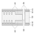
도 8은 본 발명의 일 실시예에 따른 인쇄회로기판 제조방법을 나타내는 순서도이고, 도 9 내지 도 25는 본 발명의 일 실시예에 따른 인쇄회로기판 제조방법의 각 공정을 나타내는 도면이다. 도 9 내지 도 22를 참조하면, 캐리어(10), 장벽층(12), 제1 시드층(14), 도금레지스트(16), 회로패턴(18), 절연체(20), 홀(30), 제2 시드층(40), 도전성 물질(42, 44), 솔더레지스트(50)가 도시되어 있다.8 is a flowchart illustrating a method of manufacturing a printed circuit board according to an embodiment of the present invention, and FIGS. 9 to 25 are views illustrating respective processes of the method of manufacturing a printed circuit board according to an embodiment of the present invention. 9 to 22, the
먼저, 캐리어(10)의 일면에 회로패턴(18)을 형성한다(S110). 캐리어(10)의 일면에 형성되는 회로패턴(18)은 캐리어(10)에 의해 이동되어 추후에 절연체(20)에 매립된다. 이하에서는 캐리어(10)에 회로패턴(18)을 형성하는 방법에 대해 간략히 설명하도록 한다.First, the
우선, 도 9에 도시된 바와 같이, 캐리어(10)의 일면에 장벽층(12, barrier)을 형성한다(S112). 캐리어(10)에 장벽층(12)을 형성하는 방법으로, 도금법을 이용할 수도 있고, 박막 타입의 자재를 캐리어(10)에 압착하는 방법을 이용할 수도 있다.First, as shown in FIG. 9, a
장벽층(12)은 캐리어(10)와 상이한 재질, 보다 구체적으로는 캐리어(10)가 반응하는 에칭액에 대해 반응하지 않는 재질로 이루어진다. 예를 들면, 캐리어(10)가 구리(Cu)로 이루어지는 경우, 장벽층(12)은 니켈(Ni), 크롬(Cr), 알루미늄(Al) 등과 같은 재질로 이루어질 수 있다. 이를 통해, 장벽층(12)은 추후에 에칭장벽(etch-stop)으로서의 기능을 수행할 수 있게 된다.The
그리고 나서, 역시 도 9에 도시된 바와 같이, 장벽층(12) 상에 제1 시드 층(14)을 형성한다(S114). 제1 시드층(14) 역시 장벽층(12)과 상이한 재질, 보다 구체적으로는 캐리어(10)가 반응하는 에칭액에 대해 반응하지 않는 재질로 이루어진다. 예를 들어, 전술한 바와 같이, 장벽층(12)이 니켈(Ni), 크롬(Cr), 알루미늄(Al) 등과 같은 재질로 이루어지는 경우, 제1 시드층(14)은 구리 재질로 이루어질 수 있다. 이와 같은 구리 재질의 제1 시드층(14)을 형성하기 위해, 무전해 동도금과 같은 방법을 이용할 수 있다. Then, as shown in FIG. 9, the
이 후, 도금레지스트(16)를 이용한 전해도금을 통해 제1 시드층(14) 상에 회로패턴(18)을 형성한다(S116). 즉, 도 9에 도시된 바와 같이 제1 시드층(14)의 표면에 패터닝 된 도금레지스트(16)를 형성한 후, 도 10에 도시된 바와 같이 전해도금을 수행하여 회로패턴(18)을 형성하고 나서, 도 11에 도시된 바와 같이 도금레지스트(16)를 제거함으로써 회로패턴(18)을 형성할 수 있다. 이와 같이 전해도금을 이용하여 회로패턴(18)을 형성하는 경우, 패턴 사이의 피치를 미세화할 수 있어, 고밀도 회로를 구현하는 데에 유리하다.Thereafter, the
이러한 과정을 통해 회로패턴(18)을 형성한 다음, 캐리어(10)의 일면을 절연체(20)의 일면에 압착한 후(S120), 캐리어(10)를 제거한다(S130). 즉, 도 12에 도시된 바와 같이 캐리어(10)와 절연체(20)를 정렬한 다음, 도 13에 도시된 바와 같이 이들을 압착하여 회로패턴(18)이 절연체(20)에 매립되도록 한 후, 도 14에 도시된 바와 같이 캐리어(10)를 제거하는 것이다.After the
캐리어(10)를 제거하는 방법으로는 기계적인 연마 방법을 이용할 수도 있으나, 본 실시예에서는 에칭액을 이용한 화학적인 방법을 제시하도록 한다. 니켈, 크 롬 등과 같은 재질의 장벽층(12)이 아래에 배치된 상태에서, 구리 등과 같은 재질의 캐리어(10)에 대해 에칭액을 이용한 에칭을 수행하게 되면, 해당 에칭액이 장벽층(12)에는 영향을 주지 못하므로, 장벽층(12)은 에칭장벽(etch-stop)으로서의 기능을 수행할 수 있게 되어, 에칭 깊이 제어를 보다 효율적으로 수행할 수 있게 되기 때문이다.As a method of removing the
그 다음으로, 도 16에 도시된 바와 같이, 회로패턴(18)의 일단(18')을 가공하여 절연체(20)를 관통하는 홀(30)을 형성한다(S140). 이 때, 홀(30)이 가공되는 회로패턴(18)의 일단(18')에는 비아랜드가 형성되지 않을 수 있다. 즉, 도 15에 도시된 바와 같이, 별도의 비아랜드가 형성되지 않은 회로패턴(18)의 일단(18')을 가공하여 홀(30)을 형성하는 것이다.Next, as shown in FIG. 16, one
별도의 비아랜드가 형성되지 않은 영역(18')을 가공하여 비아를 형성하는 경우, 랜드리스 비아 구조를 구현할 수 있게 되어, 고밀도의 회로패턴(18)을 용이하게 구현할 수 있게 된다. 홀(30)을 형성하기 위하여 기계적인 드릴이 이용될 수 있으며, 가공되는 홀(30)은, 도 17에 도시된 바와 같이, 회로패턴(18)의 일단(18')을 중심으로 하는 원 형상일 수 있다.When vias are formed by
이렇게 홀(30)을 가공한 다음, 홀(30)의 내부에 비아에 상응하도록 도전성 물질을 형성한다(S150). 이에 대해 보다 구체적으로 설명하면 다음과 같다.After processing the
우선, 홀(30)의 내벽 및 장벽층(12)의 표면에 제2 시드층(40)을 형성한다(S152, 도 18). 이러한 제2 시드층(40)을 형성하기 위하여 무전해 동도금과 같은 방법을 이용할 수 있다.First, the
제2 시드층(40)을 형성한 다음에는, 전해도금을 통하여, 홀(30)의 내부 및 장벽층(12) 상에 각각 도전성 물질(42, 44)을 형성한다(S164, 도 19). 이 때, 이러한 공정은 홀(30)의 내부에 구리와 같은 도전성 물질(42)이 충전(充塡)되도록 수행될 수 있다. 즉, 홀(30) 내부에 도전성 물질(42)이 가득 찰 때까지 전해도금을 수행할 수 있는 것이다. 홀(30) 내부에 형성되는 도전성 물질(42)은 추후 층간 도통을 구현하는 비아로서의 기능을 수행하게 되므로, 기 형성된 홀(30) 내부에 도전성 물질(42)을 가득 채움으로써, 층간도통의 신뢰성을 확보하는 데에 유리한 구조를 형성할 수 있게 된다.After the
이 후, 장벽층(12) 상에 형성된 도전성 물질(44)을 제거한다(S156, 도 20). 장벽층(12) 상의 도전성 물질(44)을 제거하는 방법으로, 본 실시예에서는 에칭액을 이용하는 화학적인 방법을 제시한다. 니켈, 크롬 등과 같은 재질의 장벽층(12)이 아래에 배치된 상태에서, 구리 등과 같은 재질의 도전성 물질(44)에 대해 에칭액을 이용한 에칭을 수행하게 되면, 해당 에칭액이 장벽층(12)에는 영향을 주지 못하므로, 장벽층(12)은 에칭장벽(etch-stop)으로서의 기능을 수행할 수 있게 되어, 에칭 깊이 제어를 보다 효율적으로 수행할 수 있게 되기 때문이다.Thereafter, the
그리고 나서, 장벽층(12)을 제거한다(S158, 도 21). 장벽층(12)을 제거하는 방법으로는, 역시 에칭액을 이용한 화학적인 방법을 이용할 수 있다. 장벽층(12)과 그 아래에 위치한 제1 시드층(14)은 서로 에칭액에 대한 반응성이 상이하므로, 제1 시드층(14)에는 별다른 영향을 주지 않고 장벽층(12)만을 효율적으로 제거할 수 있게 된다.Then, the
이 후, 플래시 에칭 등을 통하여 제1 시드층(14)을 제거한 다음(S160, 도 22), 최외곽에 솔더레지스트(50)를 형성하고, 필요한 영역에 대한 표면처리를 수행한다(S170, 도 23).Thereafter, the
한편, 도 9 내지 도 22에서는 양면기판을 제조하는 경우를 예로 들어 설명을 하였으나, 도 24 및 도 25에 도시된 바와 같이, 별도의 내층기판(60) 상에 절연체(20)를 추가로 적층하는 방법을 통하여, 다층인쇄회로기판을 제조할 수도 있음은 물론이다. 이 경우, 회로패턴(18)이 모두 절연체(20)에 매립될 수도 있으나(도 24 참조), 일부 회로패턴(18)은 절연체(20)에 매립되고 나머지 회로패턴(18a)은 내층기판(60)에 매립될 수도 있다(도 25 참조).Meanwhile, in FIGS. 9 to 22, a case of manufacturing a double-sided board is described as an example. However, as illustrated in FIGS. 24 and 25, an
상기에서는 본 발명의 바람직한 실시예를 참조하여 설명하였지만, 해당 기술 분야에서 통상의 지식을 가진 자라면 하기의 특허 청구의 범위에 기재된 본 발명의 사상 및 영역으로부터 벗어나지 않는 범위 내에서 본 발명을 다양하게 수정 및 변경시킬 수 있음을 이해할 수 있을 것이다.It will be apparent to those skilled in the art that various modifications and variations can be made in the present invention without departing from the spirit or scope of the invention as defined in the appended claims. It will be understood that the invention may be varied and varied without departing from the scope of the invention.
전술한 실시예 외의 많은 실시예들이 본 발명의 특허청구범위 내에 존재한다.Many embodiments other than the above-described embodiments are within the scope of the claims of the present invention.
도 1 내지 도 7은 종래기술에 따른 인쇄회로기판 제조방법의 각 공정을 나타내는 도면.1 to 7 is a view showing each step of the method for manufacturing a printed circuit board according to the prior art.
도 8은 본 발명의 일 실시예에 따른 인쇄회로기판 제조방법을 나타내는 순서도.8 is a flow chart showing a printed circuit board manufacturing method according to an embodiment of the present invention.
도 9 내지 도 25는 본 발명의 일 실시예에 따른 인쇄회로기판 제조방법의 각 공정을 나타내는 도면.9 to 25 are views showing each step of the method for manufacturing a printed circuit board according to an embodiment of the present invention.
<도면의 주요부분에 대한 부호의 설명><Description of the symbols for the main parts of the drawings>
10: 캐리어10: carrier
12: 장벽층12: barrier layer
14: 제1 시드층14: first seed layer
16: 도금레지스트16: plating resist
18: 회로패턴18: circuit pattern
20: 절연체20: insulator
30: 홀30: hall
40: 제2 시드층40: second seed layer
42, 44: 도전성 물질42, 44: conductive material
50: 솔더레지스트50: solder resist
Claims (6)
Priority Applications (2)
| Application Number | Priority Date | Filing Date | Title |
|---|---|---|---|
| KR1020080120966A KR101013992B1 (en) | 2008-12-02 | 2008-12-02 | Printed Circuit Board Manufacturing Method |
| US12/508,224 US8197702B2 (en) | 2008-12-02 | 2009-07-23 | Manufacturing method of printed circuit board |
Applications Claiming Priority (1)
| Application Number | Priority Date | Filing Date | Title |
|---|---|---|---|
| KR1020080120966A KR101013992B1 (en) | 2008-12-02 | 2008-12-02 | Printed Circuit Board Manufacturing Method |
Publications (2)
| Publication Number | Publication Date |
|---|---|
| KR20100062361A KR20100062361A (en) | 2010-06-10 |
| KR101013992B1 true KR101013992B1 (en) | 2011-02-14 |
Family
ID=42221718
Family Applications (1)
| Application Number | Title | Priority Date | Filing Date |
|---|---|---|---|
| KR1020080120966A Expired - Fee Related KR101013992B1 (en) | 2008-12-02 | 2008-12-02 | Printed Circuit Board Manufacturing Method |
Country Status (2)
| Country | Link |
|---|---|
| US (1) | US8197702B2 (en) |
| KR (1) | KR101013992B1 (en) |
Families Citing this family (4)
| Publication number | Priority date | Publication date | Assignee | Title |
|---|---|---|---|---|
| JP5600427B2 (en) * | 2009-12-25 | 2014-10-01 | 株式会社フジクラ | Material substrate for through wiring board |
| US9368340B2 (en) | 2014-06-02 | 2016-06-14 | Lam Research Corporation | Metallization of the wafer edge for optimized electroplating performance on resistive substrates |
| CN107447243B (en) * | 2017-06-19 | 2023-07-14 | 中南大学 | A device for one-way surface modification of metal micro-arc oxidation |
| CN111312680B (en) * | 2018-12-12 | 2022-10-28 | 深南电路股份有限公司 | Bearing plate of coreless packaging substrate and preparation method |
Citations (4)
| Publication number | Priority date | Publication date | Assignee | Title |
|---|---|---|---|---|
| JP2005039233A (en) | 2003-06-27 | 2005-02-10 | Tdk Corp | Substrate having via hole and its producing process |
| KR100776248B1 (en) | 2006-11-21 | 2007-11-16 | 삼성전기주식회사 | Printed Circuit Board Manufacturing Method |
| KR20080037307A (en) * | 2006-10-25 | 2008-04-30 | 삼성전기주식회사 | Circuit board and manufacturing method |
| KR20080096985A (en) * | 2007-04-30 | 2008-11-04 | 삼성전기주식회사 | Carrier member for circuit transfer, coreless printed circuit board using the same, and manufacturing method thereof |
Family Cites Families (8)
| Publication number | Priority date | Publication date | Assignee | Title |
|---|---|---|---|---|
| US6958535B2 (en) * | 2000-09-22 | 2005-10-25 | Matsushita Electric Industrial Co., Ltd. | Thermal conductive substrate and semiconductor module using the same |
| US7537668B2 (en) * | 2004-07-21 | 2009-05-26 | Samsung Electro-Mechanics Co., Ltd. | Method of fabricating high density printed circuit board |
| KR100857165B1 (en) * | 2007-04-13 | 2008-09-05 | 삼성전기주식회사 | Circuit Board Manufacturing Method |
| KR100841987B1 (en) * | 2007-07-10 | 2008-06-27 | 삼성전기주식회사 | Multi-layer printed circuit board manufacturing method |
| KR100894178B1 (en) * | 2007-09-28 | 2009-04-22 | 삼성전기주식회사 | Printed Circuit Board Manufacturing Method |
| KR20110028951A (en) * | 2009-09-14 | 2011-03-22 | 삼성전기주식회사 | Printed circuit board and manufacturing method thereof |
| KR101012403B1 (en) * | 2009-10-19 | 2011-02-09 | 삼성전기주식회사 | Printed circuit board and manufacturing method thereof |
| US8334463B2 (en) * | 2009-10-30 | 2012-12-18 | Ibiden Co., Ltd. | Wiring board and method for manufacturing the same |
-
2008
- 2008-12-02 KR KR1020080120966A patent/KR101013992B1/en not_active Expired - Fee Related
-
2009
- 2009-07-23 US US12/508,224 patent/US8197702B2/en active Active
Patent Citations (4)
| Publication number | Priority date | Publication date | Assignee | Title |
|---|---|---|---|---|
| JP2005039233A (en) | 2003-06-27 | 2005-02-10 | Tdk Corp | Substrate having via hole and its producing process |
| KR20080037307A (en) * | 2006-10-25 | 2008-04-30 | 삼성전기주식회사 | Circuit board and manufacturing method |
| KR100776248B1 (en) | 2006-11-21 | 2007-11-16 | 삼성전기주식회사 | Printed Circuit Board Manufacturing Method |
| KR20080096985A (en) * | 2007-04-30 | 2008-11-04 | 삼성전기주식회사 | Carrier member for circuit transfer, coreless printed circuit board using the same, and manufacturing method thereof |
Also Published As
| Publication number | Publication date |
|---|---|
| US8197702B2 (en) | 2012-06-12 |
| KR20100062361A (en) | 2010-06-10 |
| US20100132876A1 (en) | 2010-06-03 |
Similar Documents
| Publication | Publication Date | Title |
|---|---|---|
| KR20090057820A (en) | Printed Circuit Board and Manufacturing Method | |
| CN101188914A (en) | Method of manufacturing printed circuit board | |
| KR20130016100A (en) | Method for manufacturing wiring board | |
| KR101013992B1 (en) | Printed Circuit Board Manufacturing Method | |
| KR100872131B1 (en) | Printed Circuit Board Manufacturing Method | |
| KR101012403B1 (en) | Printed circuit board and manufacturing method thereof | |
| KR101008929B1 (en) | Printed Circuit Board Manufacturing Method | |
| KR101044790B1 (en) | Printed Circuit Board Manufacturing Method | |
| KR20090078518A (en) | Printed Circuit Board and Manufacturing Method | |
| KR101008676B1 (en) | Printed Circuit Board Manufacturing Method | |
| KR100960954B1 (en) | Printed Circuit Board Manufacturing Method | |
| JP2003273510A (en) | Printed circuit board manufacturing method | |
| KR100803960B1 (en) | Package-on Package Substrate and Manufacturing Method Thereof | |
| US7807034B2 (en) | Manufacturing method of non-etched circuit board | |
| JP2001257474A (en) | Manufacturing method of wiring board | |
| KR100999515B1 (en) | Printed Circuit Board Manufacturing Method | |
| KR100894180B1 (en) | Printed Circuit Board Manufacturing Method | |
| KR101067074B1 (en) | Printed Circuit Board and Manufacturing Method of Printed Circuit Board | |
| KR100997801B1 (en) | Printed Circuit Board Manufacturing Method | |
| KR20090086830A (en) | Printed Circuit Board Manufacturing Method | |
| KR101171100B1 (en) | Manufacturing method for circuit board | |
| KR100976202B1 (en) | Printed Circuit Board Manufacturing Method | |
| KR100749141B1 (en) | Package-on Package Substrate and Manufacturing Method Thereof | |
| KR101363076B1 (en) | Printed circuit board and method of manufacturing the same | |
| KR100952640B1 (en) | Printed circuit board and manufacturing method thereof |
Legal Events
| Date | Code | Title | Description |
|---|---|---|---|
| A201 | Request for examination | ||
| PA0109 | Patent application |
St.27 status event code: A-0-1-A10-A12-nap-PA0109 |
|
| PA0201 | Request for examination |
St.27 status event code: A-1-2-D10-D11-exm-PA0201 |
|
| PG1501 | Laying open of application |
St.27 status event code: A-1-1-Q10-Q12-nap-PG1501 |
|
| E902 | Notification of reason for refusal | ||
| PE0902 | Notice of grounds for rejection |
St.27 status event code: A-1-2-D10-D21-exm-PE0902 |
|
| E13-X000 | Pre-grant limitation requested |
St.27 status event code: A-2-3-E10-E13-lim-X000 |
|
| P11-X000 | Amendment of application requested |
St.27 status event code: A-2-2-P10-P11-nap-X000 |
|
| P13-X000 | Application amended |
St.27 status event code: A-2-2-P10-P13-nap-X000 |
|
| E701 | Decision to grant or registration of patent right | ||
| GRNT | Written decision to grant | ||
| PE0701 | Decision of registration |
St.27 status event code: A-1-2-D10-D22-exm-PE0701 |
|
| PR0701 | Registration of establishment |
St.27 status event code: A-2-4-F10-F11-exm-PR0701 |
|
| PR1002 | Payment of registration fee |
St.27 status event code: A-2-2-U10-U11-oth-PR1002 Fee payment year number: 1 |
|
| PG1601 | Publication of registration |
St.27 status event code: A-4-4-Q10-Q13-nap-PG1601 |
|
| FPAY | Annual fee payment |
Payment date: 20131224 Year of fee payment: 4 |
|
| PR1001 | Payment of annual fee |
St.27 status event code: A-4-4-U10-U11-oth-PR1001 Fee payment year number: 4 |
|
| R18-X000 | Changes to party contact information recorded |
St.27 status event code: A-5-5-R10-R18-oth-X000 |
|
| FPAY | Annual fee payment |
Payment date: 20150202 Year of fee payment: 5 |
|
| PR1001 | Payment of annual fee |
St.27 status event code: A-4-4-U10-U11-oth-PR1001 Fee payment year number: 5 |
|
| FPAY | Annual fee payment |
Payment date: 20160111 Year of fee payment: 6 |
|
| PR1001 | Payment of annual fee |
St.27 status event code: A-4-4-U10-U11-oth-PR1001 Fee payment year number: 6 |
|
| FPAY | Annual fee payment |
Payment date: 20170102 Year of fee payment: 7 |
|
| PR1001 | Payment of annual fee |
St.27 status event code: A-4-4-U10-U11-oth-PR1001 Fee payment year number: 7 |
|
| FPAY | Annual fee payment |
Payment date: 20180102 Year of fee payment: 8 |
|
| PR1001 | Payment of annual fee |
St.27 status event code: A-4-4-U10-U11-oth-PR1001 Fee payment year number: 8 |
|
| FPAY | Annual fee payment |
Payment date: 20190103 Year of fee payment: 9 |
|
| PR1001 | Payment of annual fee |
St.27 status event code: A-4-4-U10-U11-oth-PR1001 Fee payment year number: 9 |
|
| R18-X000 | Changes to party contact information recorded |
St.27 status event code: A-5-5-R10-R18-oth-X000 |
|
| FPAY | Annual fee payment |
Payment date: 20200102 Year of fee payment: 10 |
|
| PR1001 | Payment of annual fee |
St.27 status event code: A-4-4-U10-U11-oth-PR1001 Fee payment year number: 10 |
|
| PC1903 | Unpaid annual fee |
St.27 status event code: A-4-4-U10-U13-oth-PC1903 Not in force date: 20210202 Payment event data comment text: Termination Category : DEFAULT_OF_REGISTRATION_FEE |
|
| PC1903 | Unpaid annual fee |
St.27 status event code: N-4-6-H10-H13-oth-PC1903 Ip right cessation event data comment text: Termination Category : DEFAULT_OF_REGISTRATION_FEE Not in force date: 20210202 |