KR100886712B1 - Semiconductor package and manufacturing method thereof - Google Patents
Semiconductor package and manufacturing method thereof Download PDFInfo
- Publication number
- KR100886712B1 KR100886712B1 KR1020070076022A KR20070076022A KR100886712B1 KR 100886712 B1 KR100886712 B1 KR 100886712B1 KR 1020070076022 A KR1020070076022 A KR 1020070076022A KR 20070076022 A KR20070076022 A KR 20070076022A KR 100886712 B1 KR100886712 B1 KR 100886712B1
- Authority
- KR
- South Korea
- Prior art keywords
- conductive particles
- polarity
- disposed
- connection pad
- connection pads
- Prior art date
- Legal status (The legal status is an assumption and is not a legal conclusion. Google has not performed a legal analysis and makes no representation as to the accuracy of the status listed.)
- Expired - Fee Related
Links
Images


Classifications
-
- H—ELECTRICITY
- H10—SEMICONDUCTOR DEVICES; ELECTRIC SOLID-STATE DEVICES NOT OTHERWISE PROVIDED FOR
- H10W—GENERIC PACKAGES, INTERCONNECTIONS, CONNECTORS OR OTHER CONSTRUCTIONAL DETAILS OF DEVICES COVERED BY CLASS H10
- H10W72/00—Interconnections or connectors in packages
-
- H—ELECTRICITY
- H05—ELECTRIC TECHNIQUES NOT OTHERWISE PROVIDED FOR
- H05K—PRINTED CIRCUITS; CASINGS OR CONSTRUCTIONAL DETAILS OF ELECTRIC APPARATUS; MANUFACTURE OF ASSEMBLAGES OF ELECTRICAL COMPONENTS
- H05K3/00—Apparatus or processes for manufacturing printed circuits
- H05K3/30—Assembling printed circuits with electric components, e.g. with resistors
- H05K3/32—Assembling printed circuits with electric components, e.g. with resistors electrically connecting electric components or wires to printed circuits
- H05K3/321—Assembling printed circuits with electric components, e.g. with resistors electrically connecting electric components or wires to printed circuits by conductive adhesives
- H05K3/323—Assembling printed circuits with electric components, e.g. with resistors electrically connecting electric components or wires to printed circuits by conductive adhesives by applying an anisotropic conductive adhesive layer over an array of pads
-
- H—ELECTRICITY
- H10—SEMICONDUCTOR DEVICES; ELECTRIC SOLID-STATE DEVICES NOT OTHERWISE PROVIDED FOR
- H10W—GENERIC PACKAGES, INTERCONNECTIONS, CONNECTORS OR OTHER CONSTRUCTIONAL DETAILS OF DEVICES COVERED BY CLASS H10
- H10W72/00—Interconnections or connectors in packages
- H10W72/30—Die-attach connectors
-
- H—ELECTRICITY
- H05—ELECTRIC TECHNIQUES NOT OTHERWISE PROVIDED FOR
- H05K—PRINTED CIRCUITS; CASINGS OR CONSTRUCTIONAL DETAILS OF ELECTRIC APPARATUS; MANUFACTURE OF ASSEMBLAGES OF ELECTRICAL COMPONENTS
- H05K2201/00—Indexing scheme relating to printed circuits covered by H05K1/00
- H05K2201/10—Details of components or other objects attached to or integrated in a printed circuit board
- H05K2201/10613—Details of electrical connections of non-printed components, e.g. special leads
- H05K2201/10621—Components characterised by their electrical contacts
- H05K2201/10674—Flip chip
-
- H—ELECTRICITY
- H05—ELECTRIC TECHNIQUES NOT OTHERWISE PROVIDED FOR
- H05K—PRINTED CIRCUITS; CASINGS OR CONSTRUCTIONAL DETAILS OF ELECTRIC APPARATUS; MANUFACTURE OF ASSEMBLAGES OF ELECTRICAL COMPONENTS
- H05K2203/00—Indexing scheme relating to apparatus or processes for manufacturing printed circuits covered by H05K3/00
- H05K2203/10—Using electric, magnetic and electromagnetic fields; Using laser light
- H05K2203/105—Using an electrical field; Special methods of applying an electric potential
-
- H—ELECTRICITY
- H10—SEMICONDUCTOR DEVICES; ELECTRIC SOLID-STATE DEVICES NOT OTHERWISE PROVIDED FOR
- H10W—GENERIC PACKAGES, INTERCONNECTIONS, CONNECTORS OR OTHER CONSTRUCTIONAL DETAILS OF DEVICES COVERED BY CLASS H10
- H10W72/00—Interconnections or connectors in packages
- H10W72/071—Connecting or disconnecting
- H10W72/072—Connecting or disconnecting of bump connectors
-
- H—ELECTRICITY
- H10—SEMICONDUCTOR DEVICES; ELECTRIC SOLID-STATE DEVICES NOT OTHERWISE PROVIDED FOR
- H10W—GENERIC PACKAGES, INTERCONNECTIONS, CONNECTORS OR OTHER CONSTRUCTIONAL DETAILS OF DEVICES COVERED BY CLASS H10
- H10W72/00—Interconnections or connectors in packages
- H10W72/071—Connecting or disconnecting
- H10W72/073—Connecting or disconnecting of die-attach connectors
- H10W72/07331—Connecting techniques
-
- H—ELECTRICITY
- H10—SEMICONDUCTOR DEVICES; ELECTRIC SOLID-STATE DEVICES NOT OTHERWISE PROVIDED FOR
- H10W—GENERIC PACKAGES, INTERCONNECTIONS, CONNECTORS OR OTHER CONSTRUCTIONAL DETAILS OF DEVICES COVERED BY CLASS H10
- H10W72/00—Interconnections or connectors in packages
- H10W72/071—Connecting or disconnecting
- H10W72/074—Connecting or disconnecting of anisotropic conductive adhesives
-
- H—ELECTRICITY
- H10—SEMICONDUCTOR DEVICES; ELECTRIC SOLID-STATE DEVICES NOT OTHERWISE PROVIDED FOR
- H10W—GENERIC PACKAGES, INTERCONNECTIONS, CONNECTORS OR OTHER CONSTRUCTIONAL DETAILS OF DEVICES COVERED BY CLASS H10
- H10W72/00—Interconnections or connectors in packages
- H10W72/20—Bump connectors, e.g. solder bumps or copper pillars; Dummy bumps; Thermal bumps
- H10W72/241—Dispositions, e.g. layouts
-
- H—ELECTRICITY
- H10—SEMICONDUCTOR DEVICES; ELECTRIC SOLID-STATE DEVICES NOT OTHERWISE PROVIDED FOR
- H10W—GENERIC PACKAGES, INTERCONNECTIONS, CONNECTORS OR OTHER CONSTRUCTIONAL DETAILS OF DEVICES COVERED BY CLASS H10
- H10W72/00—Interconnections or connectors in packages
- H10W72/20—Bump connectors, e.g. solder bumps or copper pillars; Dummy bumps; Thermal bumps
- H10W72/29—Bond pads specially adapted therefor
-
- H—ELECTRICITY
- H10—SEMICONDUCTOR DEVICES; ELECTRIC SOLID-STATE DEVICES NOT OTHERWISE PROVIDED FOR
- H10W—GENERIC PACKAGES, INTERCONNECTIONS, CONNECTORS OR OTHER CONSTRUCTIONAL DETAILS OF DEVICES COVERED BY CLASS H10
- H10W72/00—Interconnections or connectors in packages
- H10W72/90—Bond pads, in general
- H10W72/921—Structures or relative sizes of bond pads
- H10W72/923—Bond pads having multiple stacked layers
-
- H—ELECTRICITY
- H10—SEMICONDUCTOR DEVICES; ELECTRIC SOLID-STATE DEVICES NOT OTHERWISE PROVIDED FOR
- H10W—GENERIC PACKAGES, INTERCONNECTIONS, CONNECTORS OR OTHER CONSTRUCTIONAL DETAILS OF DEVICES COVERED BY CLASS H10
- H10W72/00—Interconnections or connectors in packages
- H10W72/90—Bond pads, in general
- H10W72/951—Materials of bond pads
- H10W72/952—Materials of bond pads comprising metals or metalloids, e.g. PbSn, Ag or Cu
-
- H—ELECTRICITY
- H10—SEMICONDUCTOR DEVICES; ELECTRIC SOLID-STATE DEVICES NOT OTHERWISE PROVIDED FOR
- H10W—GENERIC PACKAGES, INTERCONNECTIONS, CONNECTORS OR OTHER CONSTRUCTIONAL DETAILS OF DEVICES COVERED BY CLASS H10
- H10W74/00—Encapsulations, e.g. protective coatings
- H10W74/10—Encapsulations, e.g. protective coatings characterised by their shape or disposition
- H10W74/15—Encapsulations, e.g. protective coatings characterised by their shape or disposition on active surfaces of flip-chip devices, e.g. underfills
-
- H—ELECTRICITY
- H10—SEMICONDUCTOR DEVICES; ELECTRIC SOLID-STATE DEVICES NOT OTHERWISE PROVIDED FOR
- H10W—GENERIC PACKAGES, INTERCONNECTIONS, CONNECTORS OR OTHER CONSTRUCTIONAL DETAILS OF DEVICES COVERED BY CLASS H10
- H10W90/00—Package configurations
- H10W90/701—Package configurations characterised by the relative positions of pads or connectors relative to package parts
- H10W90/721—Package configurations characterised by the relative positions of pads or connectors relative to package parts of bump connectors
- H10W90/724—Package configurations characterised by the relative positions of pads or connectors relative to package parts of bump connectors between a chip and a stacked insulating package substrate, interposer or RDL
Landscapes
- Engineering & Computer Science (AREA)
- Manufacturing & Machinery (AREA)
- Microelectronics & Electronic Packaging (AREA)
- Wire Bonding (AREA)
Abstract
반도체 패키지 및 이의 제조 방법이 개시되어 있다. 반도체 패키지는 기판 몸체, 상기 기판 몸체의 일측면에 배치된 접속 패드들 및 상기 일측면과 대향하는 타측면 상에 배치되며 상기 접속 패드들과 전기적으로 연결된 볼 랜드들을 갖는 기판, 상기 접속 패드들과 대응하는 범프들을 갖는 반도체 칩 및 상기 기판 및 상기 반도체 칩 사이에 개재되는 절연 부재, 전계에 의하여 상기 절연 부재 내부에서 이동되어 상기 접속 패드 및 상기 범프의 사이에 배치되는 전기 유동성 도전 입자들을 갖는 이방성 도전 부재를 포함한다.A semiconductor package and a method of manufacturing the same are disclosed. The semiconductor package includes a substrate having a substrate body, connection pads disposed on one side of the substrate body, and ball lands disposed on the other side facing the one side and electrically connected to the connection pads. An anisotropic conductive having a semiconductor chip having corresponding bumps and an insulating member interposed between the substrate and the semiconductor chip, and electrically flowable conductive particles disposed within the insulating member by an electric field and disposed between the connection pad and the bump. Member.
반도체, 패키지, 접속 패드, 이방성 도전 부재 Semiconductor, Package, Connection Pad, Anisotropic Conductive Member
Description
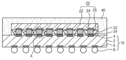
도 1은 본 발명의 일실시예에 의한 반도체 패키지를 도시한 단면도이다.1 is a cross-sectional view illustrating a semiconductor package according to an embodiment of the present invention.
도 2는 도 1의 'A' 부분 확대도이다.FIG. 2 is an enlarged view of a portion 'A' of FIG. 1.
도 3 내지 도 7들은 본 발명의 일실시예에 의한 반도체 패키지의 제조 방법을 도시한 단면도들이다.3 to 7 are cross-sectional views illustrating a method of manufacturing a semiconductor package according to an embodiment of the present invention.
본 발명은 반도체 패키지 및 이의 제조 방법에 관한 것이다.The present invention relates to a semiconductor package and a method of manufacturing the same.
최근 들어, 방대한 데이터를 저장 및 저장된 데이터를 단 시간 내 처리하는 반도체 소자를 포함하는 반도체 패키지가 개발되고 있다.In recent years, semiconductor packages including semiconductor devices for storing massive data and processing stored data in a short time have been developed.
일반적으로, 반도체 패키지는 웨이퍼 상에 트랜지스터, 저항, 커패시터 등과 같은 소자를 집적하여 반도체 칩을 형성하는 반도체 칩 제조 공정 및 반도체 칩을 웨이퍼로부터 개별화하여 외부 회로 기판 등과 전기적으로 접속 및 취성이 약한 반도체 칩을 외부로부터 인가된 충격 및/또는 진동으로부터 보호하는 패키지 공정에 의하여 제조된다.In general, a semiconductor package is a semiconductor chip manufacturing process for forming a semiconductor chip by integrating devices such as transistors, resistors, capacitors, and the like on a wafer, and a semiconductor chip having a weak electrical connection and brittleness with an external circuit board by individualizing the semiconductor chip from the wafer. It is manufactured by a package process that protects it from externally applied shocks and / or vibrations.
반도체 소자를 포함하는 반도체 패키지는 퍼스널 컴퓨터, 텔레비전 수신기, 가전 제품, 정보통신 기기 등에 폭넓게 적용되고 있다.BACKGROUND Semiconductor packages containing semiconductor devices have been widely applied to personal computers, television receivers, home appliances, information and communication devices, and the like.
최근 반도체 패키지의 기술 개발에 따라 반도체 칩의 사이즈의 100% 내지 105%에 불과한 사이즈를 갖는 "플립 칩 패키지"가 개발된 바 있다.Recently, according to the technology development of the semiconductor package, a "flip chip package" having a size of only 100% to 105% of the size of the semiconductor chip has been developed.
종래 플립 칩 패키지는 반도체 칩에 배치된 본딩 패드 및 인쇄회로기판에 형성된 접속 패드를 도전성 와이어 대신 범프로 직접 전기적으로 연결하는 구조를 갖는다.Conventional flip chip packages have a structure in which bonding pads disposed on semiconductor chips and connection pads formed on a printed circuit board are directly and electrically connected to bumps instead of conductive wires.
범프를 이용하여 반도체 칩의 본딩 패드 및 인쇄회로기판의 접속 패드를 직접 전기적으로 연결하는 플립 칩 패키지는 특히 고속으로 데이터를 저장 및/또는 처리할 수 있는 장점을 갖는다.Flip chip packages that directly connect the bonding pads of a semiconductor chip and the connection pads of a printed circuit board by using bumps have an advantage of storing and / or processing data at high speed.
그러나 종래 플립 칩 패키지의 경우 단지 범프를 이용하여 반도체 칩의 본딩 패드 및 인쇄회로기판의 접속 패드를 전기적으로 연결하기 때문에 부수적으로 반도체 칩 및 인쇄회로기판의 사이를 접착 물질 등으로 채우는 언더-필 공정을 필요로 한다.However, in the case of the conventional flip chip package, since the bumps are used to electrically connect the bonding pads of the semiconductor chip and the connection pads of the printed circuit board, the under-fill process of additionally filling the space between the semiconductor chip and the printed circuit board with an adhesive material or the like. need.
최근 도전 볼(conductive ball) 및 레진을 포함하는 이방성 도전 필름(anisotropic conductive film, ACF)을 이용하는 플립 칩 패키지가 개발된 바 있다.Recently, a flip chip package using an anisotropic conductive film (ACF) including a conductive ball and a resin has been developed.
이방성 도전 필름을 이용하는 플립 칩 패키지의 경우, 도전 볼에 의하여 반도체 칩의 본딩 패드 및 인쇄회로기판의 접속 패드가 전기적으로 접속되고, 레진이 반도체 칩 및 인쇄회로기판 사이에 형성된 갭을 채우기 때문에 별도의 언더-필 공 정을 필요로 하지 않는 장점을 갖는다.In the case of a flip chip package using an anisotropic conductive film, the bonding pad of the semiconductor chip and the connection pad of the printed circuit board are electrically connected by the conductive balls, and the resin fills the gap formed between the semiconductor chip and the printed circuit board. It has the advantage of not requiring an under-fill process.
종래 이방성 도전 필름을 이용하여 반도체 칩의 본딩 패드 및 인쇄회로기판의 접속 패드를 전기적으로 연결할 때, 본딩 패드가 이방성 도전 필름의 레진의 내부로 들어가면서 레진은 본딩 패드에 의하여 밀려나게 된다. 레진이 본딩 패드에 의하여 밀려나면서 이방성 도전 필름의 도전볼도 레진과 함께 밀려나게 되어 본딩 패드 및 인쇄회로기판의 접속 패드의 전기적 접속 불량이 발생되는 문제점을 갖는다.When the bonding pad of the semiconductor chip and the connection pad of the printed circuit board are electrically connected by using the conventional anisotropic conductive film, the resin is pushed by the bonding pad while the bonding pad enters into the resin of the anisotropic conductive film. As the resin is pushed by the bonding pad, the conductive balls of the anisotropic conductive film are pushed together with the resin, thereby causing a problem in that electrical connection between the bonding pad and the connection pad of the printed circuit board is generated.
본 발명의 하나의 목적은 반도체 칩의 본딩 패드 및 기판의 접속 패드의 접속 불량을 방지한 반도체 패키지를 제공한다.One object of the present invention is to provide a semiconductor package which prevents a poor connection between a bonding pad of a semiconductor chip and a connection pad of a substrate.
본 발명의 다른 목적은 상기 반도체 패키지의 제조 방법을 제공한다.Another object of the present invention is to provide a method of manufacturing the semiconductor package.
본 발명의 하나의 목적을 구현하기 위한 반도체 패키지는 기판 몸체, 상기 기판 몸체의 일측면에 배치된 접속 패드들 및 상기 일측면과 대향하는 타측면 상에 배치되며 상기 접속 패드들과 전기적으로 연결된 볼 랜드들을 갖는 기판, 상기 접속 패드들과 대응하는 범프들을 갖는 반도체 칩 및 상기 기판 및 상기 반도체 칩 사이에 개재되는 절연 부재, 전계에 의하여 상기 절연 부재 내부에서 이동되어 상기 접속 패드 및 상기 범프의 사이에 배치되는 전기 유동성 도전 입자들을 갖는 이방성 도전 부재를 포함한다.A semiconductor package for realizing an object of the present invention includes a substrate body, connection pads disposed on one side of the substrate body, and a ball disposed on the other side facing the one side and electrically connected to the connection pads. A substrate having lands, a semiconductor chip having bumps corresponding to the connection pads, and an insulating member interposed between the substrate and the semiconductor chip, moved within the insulating member by an electric field, between the connection pad and the bump. An anisotropic conductive member having electrically flowable conductive particles disposed therein.
반도체 패키지의 상기 전기 유동성 도전 입자들은 상기 접속 패드 및 상기 범프 사이에서 제1 밀도로 배치되고, 상기 접속 패드 이외의 영역에서는 상기 제1 밀도보다 낮은 제2 밀도로 배치된다.The electrically flowable conductive particles of the semiconductor package are disposed at a first density between the connection pad and the bump and at a second density lower than the first density in a region other than the connection pad.
반도체 패키지의 상기 각 전기유동성 도전 입자는 제1 극성을 갖는 제1 극성부 및 상기 제1 극성과 반대 극성인 제2 극성을 갖는 제2 극성부 중 적어도 하나를 갖는다.Each of the electrofluidic conductive particles of the semiconductor package has at least one of a first polar portion having a first polarity and a second polar portion having a second polarity opposite to the first polarity.
반도체 패키지의 상기 절연 부재는 접착 물질을 포함한다.The insulating member of the semiconductor package includes an adhesive material.
반도체 패키지의 상기 절연 부재는 상기 전기 유동성 도전 입자들의 유동성을 증가시키기 위해 열에 의하여 점도가 감소 되는 합성 수지 물질을 포함한다.The insulating member of the semiconductor package includes a synthetic resin material whose viscosity is reduced by heat to increase the fluidity of the electrically flowable conductive particles.
반도체 패키지의 상기 전기 유동성 도전 입자들은 상기 접속 패드 및 상기 범프 사이에서는 규칙적으로 배열되고, 상기 접속 패드 이외의 부분에 배치된 전기유동성 도전 입자들은 상대적으로 불규칙하게 배열된 것을 특징으로 하는 반도체 패키지.And wherein the electrically flowable conductive particles of the semiconductor package are regularly arranged between the connection pad and the bump, and the electrically flowable conductive particles disposed at a portion other than the connection pad are arranged relatively irregularly.
본 발명의 다른 목적을 구현하기 위한 반도체 패키지의 제조 방법은 기판 몸체, 상기 기판 몸체의 일측면 상에 배치된 접속 패드들 및 상기 일측면과 대향하는 타측면 상에 배치되며 상기 접속 패드들과 전기적으로 연결되는 볼 랜드들을 갖는 기판을 형성하는 단계, 전기장에 의하여 이동되는 전기유동성 도전 입자들 및 절연 부재를 갖는 이방성 도전 부재를 상기 기판의 상기 일측면 상에 배치하는 단계, 상기 접속 패드를 통해 상기 전기유동성 도전 입자들에 전계를 인가하여, 상기 절연 부재 내에서 상기 전기유동성 도전 입자들을 상기 접속 패드와 대응하는 부분으로 이동시켜 상기 전기 유동성 도전 입자들을 재배열하는 단계 및 상기 접속 패드와 대응하는 상기 전기유동성 도전 입자들을 이용해 반도체 칩의 범프를 상기 접속 패드에 전기적으로 접속하는 단계를 포함한다.A method of manufacturing a semiconductor package for realizing another object of the present invention includes a substrate body, connection pads disposed on one side of the substrate body, and other side surfaces facing the one side and electrically connected to the connection pads. Forming a substrate having ball lands connected to the substrate; disposing anisotropic conductive member having electrophoretic conductive particles and an insulating member moved by an electric field on the one side of the substrate; Applying an electric field to the electro-flowing conductive particles to move the electro-flowing conductive particles to a portion corresponding to the connection pad in the insulating member to rearrange the electrically-flowing conductive particles and to correspond to the connection pad. The bumps of the semiconductor chip are electrically connected to the connection pads using electrofluid conductive particles And a step of connection.
상기 전기 유동성 도전 입자들은 상기 접속 패드와 대응하는 부분에서 제1 밀도를 갖고, 상기 접속 패드 이외의 부분에서 상기 제1 밀도보다 낮은 제2 밀도를 갖는다.The electrically flowable conductive particles have a first density at portions corresponding to the connection pads, and have a second density lower than the first density at portions other than the connection pads.
상기 재배열 단계에서, 상기 이방성 도전 부재에는 열이 인가된다.In the rearrangement step, heat is applied to the anisotropic conductive member.
상기 각 전기유동성 도전 입자는 제1 극성을 갖는 제1 극성부 및 상기 제1 극성과 반대 극성인 제2 극성을 갖는 제2 극성부 중 어느 하나를 갖는다.Each of the electrofluidic conductive particles has any one of a first polar portion having a first polarity and a second polar portion having a second polarity opposite to the first polarity.
상기 각 접속 패드에는 제1 극성을 갖는 제1 전원 및 상기 제1 극성과 반대 극성인 제2 극성을 갖는 제2 전원이 인가된다.Each connection pad is supplied with a first power source having a first polarity and a second power source having a second polarity opposite to the first polarity.
짝수 번째 접속 패드들에는 상기 제1 전원이 제공되고, 홀수 번째 접속 패드들에는 상기 제2 전원이 제공된다.Even-numbered connection pads are provided with the first power source, and odd-numbered connection pads are provided with the second power source.
이하, 첨부된 도면들을 참조하여 본 발명의 실시예들에 따른 반도체 패키지 및 이의 제조 방법에 대하여 상세하게 설명하지만, 본 발명이 하기의 실시예들에 제한되는 것은 아니며, 해당 분야에서 통상의 지식을 가진 자라면 본 발명의 기술적 사상을 벗어나지 않는 범위 내에서 본 발명을 다양한 다른 형태로 구현할 수 있을 것이다.Hereinafter, a semiconductor package and a method of manufacturing the same according to embodiments of the present invention will be described in detail with reference to the accompanying drawings, but the present invention is not limited to the following embodiments, and the general knowledge in the art. Those skilled in the art can implement the present invention in various other forms without departing from the technical spirit of the present invention.
도 1은 본 발명의 일실시예에 의한 반도체 패키지를 도시한 단면도이다. 도 2는 도 1의 'A' 부분 확대도이다.1 is a cross-sectional view illustrating a semiconductor package according to an embodiment of the present invention. FIG. 2 is an enlarged view of a portion 'A' of FIG. 1.
도 1 및 도 2를 참조하면, 반도체 패키지(100)는 기판(10), 반도체 칩(20) 및 이방성 도전 부재(30)를 포함한다. 이에 더하여, 반도체 패키지(100)는 선택적으로 몰딩 부재(40)를 더 포함할 수 있다.1 and 2, the semiconductor package 100 includes a
기판(10)은 기판 몸체(2), 접속 패드(4), 볼 랜드(6) 및 도전 볼(8)을 포함한다.The
기판 몸체(2)는, 예를 들어, 플레이트 형상을 갖고, 기판 몸체(2)의 내부에는 적어도 한 층으로 이루어진 회로 패턴(미도시)을 포함한다. 기판 몸체(2)는, 예를 들어, 인쇄회로기판일 수 있다.The
접속 패드(4)는 기판 몸체(2)의 일측면 상에 배치되고, 볼 랜드(6)는 기판 몸체(2)의 일측면과 대향하는 기판 몸체(2)의 타측면 상에 배치된다. 각 접속 패드(4) 및 각 볼 랜드(6)는 기판 몸체(2)의 회로 패턴에 의하여 상호 전기적으로 연결된다.The
도전 볼(8)은 볼 랜드(6)와 전기적으로 연결되며, 도전 볼(8)은, 예를 들어, 솔더를 포함하는 솔더 볼일 수 있다.The
반도체 칩(20)은 반도체 칩 몸체(22), 본딩 패드(24) 및 범프(26)를 포함한다.The
반도체 칩 몸체(22)는 데이터를 저장하기 위한 데이터 저장부(미도시) 및 데이터를 처리하기 위한 데이터 처리부(미도시)를 포함한다.The
본딩 패드(24)는 반도체 칩 몸체(22) 상에 배치되며, 본딩 패드(24)는 데이터 저장부 및/또는 데이터 처리부와 전기적으로 연결된다. 본딩 패드(24)는, 전기적 특성이 우수한 알루미늄 또는 알루미늄 합금을 포함할 수 있다.The
범프(26)는, 예를 들어, 본딩 패드(24)와 전기적으로 연결된다. 본 실시예에서, 범프(26)는 본딩 패드(24)로부터 돌출된 스터드 범프일 수 있다. 범프(26)는 기판 몸체(2)에 형성된 접속 패드(4)와 대응하는 위치에 형성된다.The
이방성 도전 부재(30)는, 예를 들어, 필름 형상을 갖는다. 이방성 도전 부재(30)는 절연 부재(32) 및 전기유동성 도전 입자(34)를 포함한다.The anisotropic
절연 부재(32)는, 예를 들어, 열에 의하여 유동성이 증가 또는 점도가 감소하는 합성 수지 물질을 포함하고, 절연 부재(32)에는 기판(10) 및 반도체 칩(20)을 고정하기 위한 접착 물질을 포함한다.The
전기유동성 도전 입자(34)는 절연 부재(32)의 내부에 배치된다. 각 전기유동성 도전 입자(34)들은 전계(또는 자기장)에 의하여 절연 부재(32) 내에서 재배열되는 특성을 갖는다.Electrophoretic
전기유동성 도전 입자(34)가 전계에 의하여 절연 부재(32) 내에서 재배열되도록 하기 위해, 전기유동성 도전 입자(34)는 극성을 갖는다.In order for the electrofluidic
각 전기유동성 도전 입자(34)는 제1 극성, 예를 들면, (+) 극성을 갖는 제1 극성부를 가질 수 있다. 이와 다르게, 각 전기 유동성 도전 입자(34)는 제1 극성과 반대인 제2 극성, 예를 들면, (-) 극성을 갖는 제2 극성부를 가질 수 있다. 이와 다르게, 각 전기유동성 도전 입자(34)는 제1 극성을 갖는 제1 극성부 및 제2 극성을 갖는 제2 극성부가 함께 형성될 수 있다.Each electrofluidic
이방성 도전 부재(30)의 절연 부재(32) 내부에 배치되며 극성을 갖는 전기유동성 도전 입자(34)는 전계에 의하여 절연 부재(32) 내에서 이동하여 절연기판(10) 의 접속 패드(4) 및 반도체 칩(20)의 범프(26)의 사이에 집중적으로 배치된다.Electrophoretic
이와 같이 절연 부재(32) 내부에 극성을 갖는 전기유동성 도전 입자(34)가 전계에 의하여 접속 패드(4) 및 범프(26) 사이에 집중적으로 배치될 경우, 접속 패드(4) 및 범프(26)의 사이에서 전기유동성 도전 입자(34)는 제1 밀도로 배치되고, 접속 패드(4) 및 범프(26) 이외의 부분에서 전기유동성 도전 입자(34)는 제1 밀도보다 상대적으로 낮은 제2 밀도로 배치된다. 이로 인해, 범프(26) 및 접속 패드(4)가 전기유동성 도전 입자(34)에 의하여 전기적/물리적으로 결합 되는 도중 발생 되는 범프(26) 및 접속 패드(4)의 전기적 접속 불량을 방지할 수 있다.As described above, when the electrophoretic
또한, 절연 부재(32) 내부에 극성을 갖는 전기유동성 도전 입자(34)가 전계에 의하여 접속 패드(4) 및 범프(26) 사이에 집중적으로 배치될 경우, 접속 패드(4) 및 범프(26)의 사이에서 전기유동성 도전 입자(34)는 접속 패드(4) 및 범프(26) 이외의 부분 보다 규칙적으로 배치된다. 이로써, 범프(26) 및 접속 패드(4)가 전기유동성 도전 입자(34)에 의하여 전기적/물리적으로 결합 되는 도중 발생 되는 범프(26) 및 접속 패드(4)의 전기적 접속 불량을 방지할 수 있다.In addition, when the electrophoretic
도 3 내지 도 7들은 본 발명의 일실시예에 의한 반도체 패키지의 제조 방법을 도시한 단면도들이다.3 to 7 are cross-sectional views illustrating a method of manufacturing a semiconductor package according to an embodiment of the present invention.
도 3을 참조하면, 반도체 패키지를 제조하기 위해서, 예를 들어, 기판(10)이 먼저 제조된다.Referring to FIG. 3, in order to manufacture a semiconductor package, for example, the
플레이트 형상을 갖는 기판(10)은 기판 몸체(2)를 갖고, 기판 몸체(2)의 일측면 상에는 접속 패드(4)가 형성되고, 기판 몸체(2)의 일측면과 대향하는 타측면 상에는 도전성 비아(5) 등을 이용하여 접속 패드(4)와 전기적으로 연결된 볼 랜드(6)가 형성된다.The
도 4를 참조하면, 기판(10)이 제조된 후, 기판(10)의 기판 몸체(2)의 일측면 상에는 예비 이방성 도전 부재(preliminary anisotropic conductive member; 31)가 부착된다.Referring to FIG. 4, after the
예비 이방성 도전 부재(31)는 절연 부재(32) 및 절연 부재(32)의 내부에 배치된 전기유동성 도전 입자(34)를 포함한다.The preliminary anisotropic conductive member 31 includes an insulating
본 실시예에서, 절연 부재(32)는 열에 의하여 유동성은 증가 및 점도는 감소 되는 물리적 특성을 갖는 절연성 합성 수지를 포함한다. 이에 더하여 절연 부재(32)는 기판(10) 및 후술 될 반도체 칩과 고정되기 위한 접착 물질을 더 포함한다.In this embodiment, the insulating
전기유동성 도전 입자(34)는 전계에 의하여 절연 부재(32) 내부에서 이동되어 절연 부재(32)의 내부에서 재배열된다. 전기유동성 도전 입자(34)는 제1 극성을 갖는 제1 극성부를 포함한다. 이와 다르게, 전기유동성 도전 입자(34)는 제1 극성과 반대 극성을 갖는 제2 극성부를 포함한다. 이와 다르게, 전기유동성 도전 입자(34)는 제1 극성을 갖는 상기 제1 및 제2 극성부들을 모두 포함할 수 있다. 본 실시예에서, 제1 극성은, 예를 들어, (+) 극성이고, 제2 극성은, 예를 들어, (-) 극성이다.The electrofluid
전기유동성 도전 입자(34)는 예비 이방성 도전 부재(31)의 절연 부재(32)의 내부에 불규칙하게 배치되어 있다.The electrofluidic
도 5 및 도 6을 참조하면, 예비 이방성 도전 부재(31)가 기판 몸체(2)의 접속 패드(4)에 부착된 후, 예비 이방성 도전 부재(31)의 전기유동성 도전 입자(34)에 전계가 인가되어 전기유동성 도전 입자(34)는 재배열된다.5 and 6, after the preliminary anisotropic conductive member 31 is attached to the
전기유동성 도전 입자(34)를 재배열하기 위하여 예비 이방성 도전 부재(31)에 포함된 전기유동성 도전 입자(34)는, 예를 들어, (+) 극성을 갖는 제1 극성부를 가질 수 있다. 전기유동성 도전 입자(34)가, 예를 들어, (+) 극성을 가질 경우, 접속 패드(4)와 전기적으로 연결된 볼 랜드(6)에는 전원 인가 부재(50)로부터 제공된 (-) 극성을 갖는 전원이 인가된다.The electrofluid
(-) 극성을 갖는 전원이 볼 랜드(6)로부터 접속 패드(4)에 제공될 경우, (+) 극성을 갖는 제1 극성부를 갖는 전기유동성 도전 입자(34)는 인력에 의하여 접속 패드(4) 부분으로 이동되어, 재배열된 전기유동성 도전 입자(34)를 갖는 이방성 도전 부재(30)가 제조된다.When a power source having a negative polarity is provided to the
이때, 전기유동성 도전 입자(34)가 보다 쉽게 접속 패드(4) 부분으로 이동되도록 예비 이방성 도전 부재(31)는 소정 온도로 가열될 수 있다.In this case, the preliminary anisotropic conductive member 31 may be heated to a predetermined temperature so that the electrofluidic
재배열된 전기유동성 도전 입자(34)는 제1 밀도를 갖고, 접속 패드(4) 이외의 부분에서는 제1 밀도보다 낮은 제2 밀도를 갖는다. 또한, 접속 패드(4) 부분에서 제1 밀도를 갖는 전기유동성 도전 입자(34)는 비교적 규칙적으로 재배열된다.The rearranged electrofluidic
한편, 전기유동성 도전 입자(34)를 재배열하기 위하여 예비 이방성 도전 부재(31)에 포함된 전기유동성 도전 입자(34)는, 예를 들어, (-) 극성을 갖는 제2 극성부를 가질 수 있다. 전기유동성 도전 입자(34)가, 예를 들어, (-) 극성을 가질 경우, 접속 패드(4)와 전기적으로 연결된 볼 랜드(6)에는 전원 인가 부재(50)로부터 제공된 (+) 극성을 갖는 전원이 인가된다.Meanwhile, the electrofluid
(+) 극성을 갖는 전원이 볼 랜드(6)로부터 접속 패드(4)에 제공될 경우, (-) 극성을 갖는 제2 극성부를 갖는 전기유동성 도전 입자(34)는 인력에 의하여 접속 패드(4) 부분으로 이동되어, 재배열된 전기유동성 도전 입자(34)를 갖는 이방성 도전 부재(30)가 제조된다.When a power source having a positive polarity is provided to the
이때, 전기유동성 도전 입자(34)가 보다 쉽게 접속 패드(4) 부분으로 이동되도록 예비 이방성 도전 부재(31)는 소정 온도로 가열될 수 있다. In this case, the preliminary anisotropic conductive member 31 may be heated to a predetermined temperature so that the electrofluidic
재배열된 전기유동성 도전 입자(34)는 제1 밀도를 갖고, 접속 패드(4) 이외의 부분에서는 제1 밀도보다 낮은 제2 밀도를 갖는다. 또한, 접속 패드(4) 부분에서 제1 밀도를 갖는 전기유동성 도전 입자(34)는 비교적 규칙적으로 재배열된다.The rearranged electrofluidic
한편, 전기유동성 도전 입자(34)를 재배열하기 위하여 예비 이방성 도전 부재(31)에 포함된 각 전기유동성 도전 입자(34)는, 예를 들어, (+) 극성을 갖는 제1 극성부 및 (-) 극성을 갖는 제2 극성부를 함께 가질 수 있다.On the other hand, in order to rearrange the electrofluidic
접속 패드(4)와 전기적으로 연결된 볼 랜드(6)에 전원 인가 부재(50)로부터 제공된 (+) 극성을 갖는 전원 또는 (-) 극성을 갖는 전원이 인가될 경우, 전기유동성 도전 입자(34)는 인력에 의하여 접속 패드(4) 부분으로 이동되어, 재배열된 전기유동성 도전 입자(34)를 갖는 이방성 도전 부재(30)가 제조된다.The electrofluidic
이때, 전기유동성 도전 입자(34)가 보다 쉽게 접속 패드(4) 부분으로 이동되도록 예비 이방성 도전 부재(31)는 소정 온도로 가열될 수 있다.In this case, the preliminary anisotropic conductive member 31 may be heated to a predetermined temperature so that the electrofluidic
재배열된 전기유동성 도전 입자(34)는 제1 밀도를 갖고, 접속 패드(4) 이외의 부분에서는 제1 밀도보다 낮은 제2 밀도를 갖는다. 또한, 접속 패드(4) 부분에서 제1 밀도를 갖는 전기유동성 도전 입자(34)는 비교적 규칙적으로 재배열된다.The rearranged electrofluidic
전기유동성 도전 입자(34)가 제1 극성부 및 제2 극성부를 함께 가질 경우, 짝수 번째 접속 패드(4)에는 (-) 극성을 갖는 전원이 제공되고, 홀수 번째 접속 패드(4)에는 (+) 극성을 갖는 전원이 제공될 수 있고, 이 결과, 전기유동성 도전 입자(34)들은 절연 부재(32) 내에서 인접한 2 개의 접속 패드(4)들을 연결하는 반원 고리 형상으로 배치될 수 있다.When the electrofluidic
도 7을 참조하면, 기판(10) 상에 재배열된 전기유동성 도전 입자를 갖는 이방성 도전 부재(30)가 부착된 후, 이방성 도전 부재(30)에는 반도체 칩(20)이 부착된다.Referring to FIG. 7, after the anisotropic
반도체 칩(20)은 반도체 칩 몸체(22), 본딩 패드(24) 및 범프(26)를 포함한다. 이때, 반도체 칩(20)의 본딩 패드(24)는 기판(10) 상에 형성된 접속 패드(4)와 대응하는 위치에 형성되고, 본딩 패드(24)에는 범프(26)가 전기적으로 접속된다.The
범프(26)는 전기유동성 도전 입자(24)가 재배열된 이방성 도전 부재(30)의 내부로 제공되어 범프(26), 전기유동성 도전 입자(34) 및 접속 패드(4)는 전기적/물리적으로 접속된다.The
이상에서 상세하게 설명한 바에 의하면, 이방성 도전 부재의 내부에 전계에 의하여 재배열되는 전기유동성 도전 입자를 배치하고, 접속 패드에 전계를 형성하 여 전기유동성 도전 입자를 이방성 도전 부재의 내부에서 재배열하여 접속 패드 및 반도체 칩의 범프 사이의 전기적 접속 불량을 방지하는 효과를 갖는다.As described in detail above, the electrofluid conductive particles rearranged by an electric field are disposed inside the anisotropic conductive member, an electric field is formed on the connection pad, and the electrofluid conductive particles are rearranged inside the anisotropic conductive member. The electrical connection between the connection pad and the bump of the semiconductor chip is prevented.
앞서 설명한 본 발명의 상세한 설명에서는 본 발명의 실시예들을 참조하여 설명하였지만, 해당 기술분야의 숙련된 당업자 또는 해당 기술분야에 통상의 지식을 갖는 자라면 후술 될 특허청구범위에 기재된 본 발명의 사상 및 기술 영역으로부터 벗어나지 않는 범위 내에서 본 발명을 다양하게 수정 및 변경시킬 수 있음을 이해할 수 있을 것이다.In the detailed description of the present invention described above with reference to the embodiments of the present invention, those skilled in the art or those skilled in the art having ordinary knowledge in the scope of the present invention described in the claims and It will be appreciated that various modifications and variations can be made in the present invention without departing from the scope of the art.
Claims (12)
Priority Applications (3)
| Application Number | Priority Date | Filing Date | Title |
|---|---|---|---|
| KR1020070076022A KR100886712B1 (en) | 2007-07-27 | 2007-07-27 | Semiconductor package and manufacturing method thereof |
| US12/043,314 US20090026612A1 (en) | 2007-07-27 | 2008-03-06 | Semiconductor package having an improved connection structure and method for manufacturing the same |
| US13/329,937 US20120088336A1 (en) | 2007-07-27 | 2011-12-19 | Semiconductor package having an improved connection structure and method for manufacturing the same |
Applications Claiming Priority (1)
| Application Number | Priority Date | Filing Date | Title |
|---|---|---|---|
| KR1020070076022A KR100886712B1 (en) | 2007-07-27 | 2007-07-27 | Semiconductor package and manufacturing method thereof |
Publications (2)
| Publication Number | Publication Date |
|---|---|
| KR20090011955A KR20090011955A (en) | 2009-02-02 |
| KR100886712B1 true KR100886712B1 (en) | 2009-03-04 |
Family
ID=40294540
Family Applications (1)
| Application Number | Title | Priority Date | Filing Date |
|---|---|---|---|
| KR1020070076022A Expired - Fee Related KR100886712B1 (en) | 2007-07-27 | 2007-07-27 | Semiconductor package and manufacturing method thereof |
Country Status (2)
| Country | Link |
|---|---|
| US (2) | US20090026612A1 (en) |
| KR (1) | KR100886712B1 (en) |
Families Citing this family (6)
| Publication number | Priority date | Publication date | Assignee | Title |
|---|---|---|---|---|
| US8883559B2 (en) * | 2009-09-25 | 2014-11-11 | Stats Chippac, Ltd. | Semiconductor device and method of forming adhesive material to secure semiconductor die to carrier in WLCSP |
| CN102738101A (en) * | 2011-04-13 | 2012-10-17 | 华东科技股份有限公司 | Semiconductor stereoscopic packaging structure |
| KR101490844B1 (en) * | 2014-02-11 | 2015-02-06 | 에이치엔에스하이텍 (주) | Circuit connecting method, using anisotropic conductive adhesives with organometallic compound |
| JP7185252B2 (en) | 2018-01-31 | 2022-12-07 | 三国電子有限会社 | Method for producing connection structure |
| JP7046351B2 (en) | 2018-01-31 | 2022-04-04 | 三国電子有限会社 | How to make a connection structure |
| JP7160302B2 (en) | 2018-01-31 | 2022-10-25 | 三国電子有限会社 | CONNECTED STRUCTURE AND METHOD OF MAKING CONNECTED STRUCTURE |
Citations (1)
| Publication number | Priority date | Publication date | Assignee | Title |
|---|---|---|---|---|
| US20020098620A1 (en) * | 2001-01-24 | 2002-07-25 | Yi-Chuan Ding | Chip scale package and manufacturing method thereof |
Family Cites Families (40)
| Publication number | Priority date | Publication date | Assignee | Title |
|---|---|---|---|---|
| US3841732A (en) * | 1970-03-04 | 1974-10-15 | A Marks | Dipolar electro-optic structures and method |
| US4667401A (en) * | 1985-11-26 | 1987-05-26 | Clements James R | Method of making an electronic device using an uniaxial conductive adhesive |
| US7198969B1 (en) * | 1990-09-24 | 2007-04-03 | Tessera, Inc. | Semiconductor chip assemblies, methods of making same and components for same |
| AU6015596A (en) * | 1995-06-13 | 1997-01-09 | Hitachi Chemical Company, Ltd. | Semiconductor device, wiring board for mounting semiconducto r and method of production of semiconductor device |
| US5736074A (en) * | 1995-06-30 | 1998-04-07 | Micro Fab Technologies, Inc. | Manufacture of coated spheres |
| US5661042A (en) * | 1995-08-28 | 1997-08-26 | Motorola, Inc. | Process for electrically connecting electrical devices using a conductive anisotropic material |
| JP2908747B2 (en) * | 1996-01-10 | 1999-06-21 | 三菱電機株式会社 | IC socket |
| US6103359A (en) * | 1996-05-22 | 2000-08-15 | Jsr Corporation | Process and apparatus for manufacturing an anisotropic conductor sheet and a magnetic mold piece for the same |
| JPH1084014A (en) * | 1996-07-19 | 1998-03-31 | Shinko Electric Ind Co Ltd | Method for manufacturing semiconductor device |
| US6190509B1 (en) * | 1997-03-04 | 2001-02-20 | Tessera, Inc. | Methods of making anisotropic conductive elements for use in microelectronic packaging |
| JPH1140224A (en) * | 1997-07-11 | 1999-02-12 | Jsr Corp | Anisotropic conductive sheet |
| US20070102827A1 (en) * | 1997-12-08 | 2007-05-10 | 3M Innovative Properties Company | Solvent Assisted Burnishing of Pre-Underfilled Solder-Bumped Wafers for Flipchip Bonding |
| US6492738B2 (en) * | 1999-09-02 | 2002-12-10 | Micron Technology, Inc. | Apparatus and methods of testing and assembling bumped devices using an anisotropically conductive layer |
| TW561266B (en) * | 1999-09-17 | 2003-11-11 | Jsr Corp | Anisotropic conductive sheet, its manufacturing method, and connector |
| JP4240724B2 (en) * | 2000-01-26 | 2009-03-18 | Jsr株式会社 | Anisotropic conductive sheet and connector |
| JP3427086B2 (en) * | 2000-02-23 | 2003-07-14 | Necエレクトロニクス株式会社 | IC socket |
| US6346750B1 (en) * | 2000-04-28 | 2002-02-12 | Micron Technology, Inc. | Resistance-reducing conductive adhesives for attachment of electronic components |
| US7064432B2 (en) * | 2000-07-26 | 2006-06-20 | The Research Foundation Of State University Of New York | Method and system for bonding a semiconductor chip onto a carrier using micro-pins |
| JP2002075064A (en) * | 2000-08-23 | 2002-03-15 | Tdk Corp | Anisotropic conductive film and its manufacturing method, and display using anisotropic conductive film |
| EP1195860B1 (en) * | 2000-09-25 | 2004-12-01 | JSR Corporation | Anisotropically conductive sheet, production process thereof and applied product thereof |
| KR20030078870A (en) * | 2000-12-08 | 2003-10-08 | 제이에스알 가부시끼가이샤 | Anisotropic conductive sheet and wafer inspection device |
| JP2002299378A (en) * | 2001-03-30 | 2002-10-11 | Lintec Corp | Adhesive sheet with conductor, semiconductor device manufacturing method and semiconductor device |
| JP2003149291A (en) * | 2001-11-13 | 2003-05-21 | Unitechno Inc | Contact structure |
| US6733613B2 (en) * | 2002-07-25 | 2004-05-11 | S. Kumar Khanna | Method for curing an anisotropic conductive compound |
| KR100756707B1 (en) * | 2002-08-09 | 2007-09-07 | 제이에스알 가부시끼가이샤 | Anisotropic conductivity connector, conductive paste composition, probe member, and wafer inspecting device |
| ATE367650T1 (en) * | 2002-08-09 | 2007-08-15 | Jsr Corp | TEST CONNECTOR WITH ANISOTROPIC CONDUCTIVITY |
| US6841883B1 (en) * | 2003-03-31 | 2005-01-11 | Micron Technology, Inc. | Multi-dice chip scale semiconductor components and wafer level methods of fabrication |
| TWI239685B (en) * | 2003-05-13 | 2005-09-11 | Jsr Corp | Flaky probe, its manufacturing method and its application |
| CN1806178A (en) * | 2003-06-09 | 2006-07-19 | Jsr株式会社 | Anisotropic conductive connector and wafer inspection device |
| US7309244B2 (en) * | 2003-06-12 | 2007-12-18 | Jsr Corporation | Anisotropic conductive connector device and production method therefor and circuit device inspection device |
| US7081675B2 (en) * | 2004-08-16 | 2006-07-25 | Telephus Inc. | Multilayered anisotropic conductive adhesive for fine pitch |
| KR100733208B1 (en) * | 2004-10-11 | 2007-06-27 | 삼성전기주식회사 | Semiconductor package using filp-chip mounting technology |
| KR100669830B1 (en) * | 2004-11-16 | 2007-04-16 | 삼성전자주식회사 | Multilayer Package Using Anisotropic Conductive Film |
| US20060170096A1 (en) * | 2005-02-02 | 2006-08-03 | Yang Jun Y | Chip scale package and method for manufacturing the same |
| CN100495677C (en) * | 2005-03-29 | 2009-06-03 | 松下电器产业株式会社 | Flip chip packaging method and bump forming method |
| JP4084835B2 (en) * | 2005-03-29 | 2008-04-30 | 松下電器産業株式会社 | Flip chip mounting method and inter-board connection method |
| US7663232B2 (en) * | 2006-03-07 | 2010-02-16 | Micron Technology, Inc. | Elongated fasteners for securing together electronic components and substrates, semiconductor device assemblies including such fasteners, and accompanying systems |
| US7537961B2 (en) * | 2006-03-17 | 2009-05-26 | Panasonic Corporation | Conductive resin composition, connection method between electrodes using the same, and electric connection method between electronic component and circuit substrate using the same |
| WO2007125789A1 (en) * | 2006-04-27 | 2007-11-08 | Panasonic Corporation | Connection structure and method of producing the same |
| KR100842921B1 (en) * | 2007-06-18 | 2008-07-02 | 주식회사 하이닉스반도체 | Manufacturing method of semiconductor package |
-
2007
- 2007-07-27 KR KR1020070076022A patent/KR100886712B1/en not_active Expired - Fee Related
-
2008
- 2008-03-06 US US12/043,314 patent/US20090026612A1/en not_active Abandoned
-
2011
- 2011-12-19 US US13/329,937 patent/US20120088336A1/en not_active Abandoned
Patent Citations (2)
| Publication number | Priority date | Publication date | Assignee | Title |
|---|---|---|---|---|
| US20020098620A1 (en) * | 2001-01-24 | 2002-07-25 | Yi-Chuan Ding | Chip scale package and manufacturing method thereof |
| US20020142518A1 (en) | 2001-01-24 | 2002-10-03 | Yi-Chuan Ding | Chip scale package and manufacturing method |
Also Published As
| Publication number | Publication date |
|---|---|
| US20090026612A1 (en) | 2009-01-29 |
| US20120088336A1 (en) | 2012-04-12 |
| KR20090011955A (en) | 2009-02-02 |
Similar Documents
| Publication | Publication Date | Title |
|---|---|---|
| KR102198858B1 (en) | Semiconductor package stack structure having interposer substrate | |
| US6287892B1 (en) | Shock-resistant semiconductor device and method for producing same | |
| TWI479630B (en) | Enhanced stacked microelectronic assembly with central contacts and its system, module and configuration | |
| JP4332567B2 (en) | Manufacturing method and mounting method of semiconductor device | |
| KR101710178B1 (en) | An embedded chip on chip package and package on package including the same | |
| US20150221625A1 (en) | Semiconductor package having a dissipating plate | |
| CN103811472A (en) | Semiconductor package and manufacturing method thereof | |
| US20150022985A1 (en) | Device-embedded package substrate and semiconductor package including the same | |
| US20140124906A1 (en) | Semiconductor package and method of manufacturing the same | |
| US20100155920A1 (en) | Stacked semiconductor package, semiconductor package module and method of manufacturing the stacked semiconductor package | |
| TWI778236B (en) | semiconductor device | |
| US9392695B2 (en) | Electric component module | |
| CN104584212A (en) | Stacked die package including die in package substrate | |
| KR100886712B1 (en) | Semiconductor package and manufacturing method thereof | |
| TW201351579A (en) | High density three-dimensional package | |
| CN105977231A (en) | Composite solder ball, semiconductor package, semiconductor device and manufacturing method | |
| US20170287873A1 (en) | Electronic assembly components with corner adhesive for warpage reduction during thermal processing | |
| CN103077939A (en) | Semiconductor package including semiconductor chip with through opening | |
| KR101847162B1 (en) | Semiconductor package and method for manufacturing the same | |
| US7994428B2 (en) | Electronic carrier board | |
| JP2011258794A (en) | Electronic apparatus and method of manufacturing the same | |
| JP4952365B2 (en) | Electronic component mounting structure on a double-sided mounting circuit board, semiconductor device, and manufacturing method of double-sided mounting semiconductor device | |
| US9997504B2 (en) | Electronic device module and method of manufacturing the same | |
| CN103379736B (en) | Printed circuit board assembly and method of making the same | |
| JP6323672B2 (en) | Semiconductor device and manufacturing method thereof |
Legal Events
| Date | Code | Title | Description |
|---|---|---|---|
| A201 | Request for examination | ||
| PA0109 | Patent application |
St.27 status event code: A-0-1-A10-A12-nap-PA0109 |
|
| PA0201 | Request for examination |
St.27 status event code: A-1-2-D10-D11-exm-PA0201 |
|
| D13-X000 | Search requested |
St.27 status event code: A-1-2-D10-D13-srh-X000 |
|
| D14-X000 | Search report completed |
St.27 status event code: A-1-2-D10-D14-srh-X000 |
|
| E902 | Notification of reason for refusal | ||
| PE0902 | Notice of grounds for rejection |
St.27 status event code: A-1-2-D10-D21-exm-PE0902 |
|
| E13-X000 | Pre-grant limitation requested |
St.27 status event code: A-2-3-E10-E13-lim-X000 |
|
| P11-X000 | Amendment of application requested |
St.27 status event code: A-2-2-P10-P11-nap-X000 |
|
| P13-X000 | Application amended |
St.27 status event code: A-2-2-P10-P13-nap-X000 |
|
| PG1501 | Laying open of application |
St.27 status event code: A-1-1-Q10-Q12-nap-PG1501 |
|
| E701 | Decision to grant or registration of patent right | ||
| PE0701 | Decision of registration |
St.27 status event code: A-1-2-D10-D22-exm-PE0701 |
|
| GRNT | Written decision to grant | ||
| PR0701 | Registration of establishment |
St.27 status event code: A-2-4-F10-F11-exm-PR0701 |
|
| PR1002 | Payment of registration fee |
St.27 status event code: A-2-2-U10-U11-oth-PR1002 Fee payment year number: 1 |
|
| PG1601 | Publication of registration |
St.27 status event code: A-4-4-Q10-Q13-nap-PG1601 |
|
| LAPS | Lapse due to unpaid annual fee | ||
| PC1903 | Unpaid annual fee |
St.27 status event code: A-4-4-U10-U13-oth-PC1903 Not in force date: 20120226 Payment event data comment text: Termination Category : DEFAULT_OF_REGISTRATION_FEE |
|
| PN2301 | Change of applicant |
St.27 status event code: A-5-5-R10-R13-asn-PN2301 St.27 status event code: A-5-5-R10-R11-asn-PN2301 |
|
| PN2301 | Change of applicant |
St.27 status event code: A-5-5-R10-R13-asn-PN2301 St.27 status event code: A-5-5-R10-R11-asn-PN2301 |
|
| PC1903 | Unpaid annual fee |
St.27 status event code: N-4-6-H10-H13-oth-PC1903 Ip right cessation event data comment text: Termination Category : DEFAULT_OF_REGISTRATION_FEE Not in force date: 20120226 |
|
| PN2301 | Change of applicant |
St.27 status event code: A-5-5-R10-R13-asn-PN2301 St.27 status event code: A-5-5-R10-R11-asn-PN2301 |
|
| P22-X000 | Classification modified |
St.27 status event code: A-4-4-P10-P22-nap-X000 |