KR100871768B1 - Semiconductor element and COA / COA manufacturing method - Google Patents
Semiconductor element and COA / COA manufacturing method Download PDFInfo
- Publication number
- KR100871768B1 KR100871768B1 KR1020070048576A KR20070048576A KR100871768B1 KR 100871768 B1 KR100871768 B1 KR 100871768B1 KR 1020070048576 A KR1020070048576 A KR 1020070048576A KR 20070048576 A KR20070048576 A KR 20070048576A KR 100871768 B1 KR100871768 B1 KR 100871768B1
- Authority
- KR
- South Korea
- Prior art keywords
- metal
- coa
- oxide film
- deposited
- oxide
- Prior art date
- Legal status (The legal status is an assumption and is not a legal conclusion. Google has not performed a legal analysis and makes no representation as to the accuracy of the status listed.)
- Expired - Fee Related
Links
Images


Classifications
-
- H—ELECTRICITY
- H10—SEMICONDUCTOR DEVICES; ELECTRIC SOLID-STATE DEVICES NOT OTHERWISE PROVIDED FOR
- H10W—GENERIC PACKAGES, INTERCONNECTIONS, CONNECTORS OR OTHER CONSTRUCTIONAL DETAILS OF DEVICES COVERED BY CLASS H10
- H10W72/00—Interconnections or connectors in packages
- H10W72/20—Bump connectors, e.g. solder bumps or copper pillars; Dummy bumps; Thermal bumps
-
- H—ELECTRICITY
- H10—SEMICONDUCTOR DEVICES; ELECTRIC SOLID-STATE DEVICES NOT OTHERWISE PROVIDED FOR
- H10D—INORGANIC ELECTRIC SEMICONDUCTOR DEVICES
- H10D64/00—Electrodes of devices having potential barriers
- H10D64/01—Manufacture or treatment
- H10D64/011—Manufacture or treatment of electrodes ohmically coupled to a semiconductor
-
- H—ELECTRICITY
- H10—SEMICONDUCTOR DEVICES; ELECTRIC SOLID-STATE DEVICES NOT OTHERWISE PROVIDED FOR
- H10W—GENERIC PACKAGES, INTERCONNECTIONS, CONNECTORS OR OTHER CONSTRUCTIONAL DETAILS OF DEVICES COVERED BY CLASS H10
- H10W72/00—Interconnections or connectors in packages
- H10W72/01—Manufacture or treatment
- H10W72/012—Manufacture or treatment of bump connectors, dummy bumps or thermal bumps
- H10W72/01231—Manufacture or treatment of bump connectors, dummy bumps or thermal bumps using blanket deposition
-
- H—ELECTRICITY
- H10—SEMICONDUCTOR DEVICES; ELECTRIC SOLID-STATE DEVICES NOT OTHERWISE PROVIDED FOR
- H10W—GENERIC PACKAGES, INTERCONNECTIONS, CONNECTORS OR OTHER CONSTRUCTIONAL DETAILS OF DEVICES COVERED BY CLASS H10
- H10W72/00—Interconnections or connectors in packages
- H10W72/01—Manufacture or treatment
- H10W72/012—Manufacture or treatment of bump connectors, dummy bumps or thermal bumps
- H10W72/01251—Changing the shapes of bumps
- H10W72/01255—Changing the shapes of bumps by using masks
-
- H—ELECTRICITY
- H10—SEMICONDUCTOR DEVICES; ELECTRIC SOLID-STATE DEVICES NOT OTHERWISE PROVIDED FOR
- H10W—GENERIC PACKAGES, INTERCONNECTIONS, CONNECTORS OR OTHER CONSTRUCTIONAL DETAILS OF DEVICES COVERED BY CLASS H10
- H10W72/00—Interconnections or connectors in packages
- H10W72/01—Manufacture or treatment
- H10W72/019—Manufacture or treatment of bond pads
- H10W72/01971—Cleaning, e.g. oxide removal
-
- H—ELECTRICITY
- H10—SEMICONDUCTOR DEVICES; ELECTRIC SOLID-STATE DEVICES NOT OTHERWISE PROVIDED FOR
- H10W—GENERIC PACKAGES, INTERCONNECTIONS, CONNECTORS OR OTHER CONSTRUCTIONAL DETAILS OF DEVICES COVERED BY CLASS H10
- H10W72/00—Interconnections or connectors in packages
- H10W72/071—Connecting or disconnecting
- H10W72/072—Connecting or disconnecting of bump connectors
- H10W72/07251—Connecting or disconnecting of bump connectors characterised by changes in properties of the bump connectors during connecting
-
- H—ELECTRICITY
- H10—SEMICONDUCTOR DEVICES; ELECTRIC SOLID-STATE DEVICES NOT OTHERWISE PROVIDED FOR
- H10W—GENERIC PACKAGES, INTERCONNECTIONS, CONNECTORS OR OTHER CONSTRUCTIONAL DETAILS OF DEVICES COVERED BY CLASS H10
- H10W72/00—Interconnections or connectors in packages
- H10W72/20—Bump connectors, e.g. solder bumps or copper pillars; Dummy bumps; Thermal bumps
- H10W72/251—Materials
- H10W72/252—Materials comprising solid metals or solid metalloids, e.g. PbSn, Ag or Cu
-
- H—ELECTRICITY
- H10—SEMICONDUCTOR DEVICES; ELECTRIC SOLID-STATE DEVICES NOT OTHERWISE PROVIDED FOR
- H10W—GENERIC PACKAGES, INTERCONNECTIONS, CONNECTORS OR OTHER CONSTRUCTIONAL DETAILS OF DEVICES COVERED BY CLASS H10
- H10W72/00—Interconnections or connectors in packages
- H10W72/20—Bump connectors, e.g. solder bumps or copper pillars; Dummy bumps; Thermal bumps
- H10W72/29—Bond pads specially adapted therefor
-
- H—ELECTRICITY
- H10—SEMICONDUCTOR DEVICES; ELECTRIC SOLID-STATE DEVICES NOT OTHERWISE PROVIDED FOR
- H10W—GENERIC PACKAGES, INTERCONNECTIONS, CONNECTORS OR OTHER CONSTRUCTIONAL DETAILS OF DEVICES COVERED BY CLASS H10
- H10W72/00—Interconnections or connectors in packages
- H10W72/90—Bond pads, in general
- H10W72/951—Materials of bond pads
- H10W72/952—Materials of bond pads comprising metals or metalloids, e.g. PbSn, Ag or Cu
-
- Y—GENERAL TAGGING OF NEW TECHNOLOGICAL DEVELOPMENTS; GENERAL TAGGING OF CROSS-SECTIONAL TECHNOLOGIES SPANNING OVER SEVERAL SECTIONS OF THE IPC; TECHNICAL SUBJECTS COVERED BY FORMER USPC CROSS-REFERENCE ART COLLECTIONS [XRACs] AND DIGESTS
- Y10—TECHNICAL SUBJECTS COVERED BY FORMER USPC
- Y10T—TECHNICAL SUBJECTS COVERED BY FORMER US CLASSIFICATION
- Y10T428/00—Stock material or miscellaneous articles
- Y10T428/12—All metal or with adjacent metals
- Y10T428/12493—Composite; i.e., plural, adjacent, spatially distinct metal components [e.g., layers, joint, etc.]
- Y10T428/12528—Semiconductor component
Landscapes
- Internal Circuitry In Semiconductor Integrated Circuit Devices (AREA)
Abstract
본 발명은 금속 듀얼 다마신 공정을 이용하여 BOAC/COA를 구현하기 위한 것으로, 이를 위한 본 발명은, 반도체 기판 상에 전도성 패드 및 패시베이션 산화막을 형성하며, 형성된 전도성 패드 및 패시베이션 산화막 상부에 산화막(Oxide)을 전면 증착하며, 증착된 산화막의 일부를 선택적으로 제거하여 Bond pad가 형성될 영역을 정의하기 위한 산화막 패턴을 형성하며, 형성된 산화막 패턴 상부에 베리어막 및 금속 씨드(Seed)를 전면 증착하며, 증착된 금속 씨드 상부에 금속을 전면 증착하며, 증착된 금속에 대하여 산화막 패턴과 일부의 베리어막 및 금속 씨드가 노출될 때까지 평탄화하며, 노출된 산화막 패턴만을 식각을 통해 제거하여 BOAC/COA를 제조한다. 따라서, 기존에서와 같이 황산 배스(bath)에 의해 PR이 녹게 되어 금속 증착이 비정상적으로 이루어지는 문제점과, 그리고 스트리밍 공정에서 동일한 금속 물질에 의해 데미지가 발생되는 문제점을 해결할 수 있어 반도체 소자의 수율 및 신뢰성을 향상시킬 수 있으며, 또한 반도체 소자의 수율 및 신뢰성이 향상되어 원가 절감 및 소자 성능을 향상시킬 수 있다. The present invention is to implement a BOAC / COA using a metal dual damascene process, the present invention for forming a conductive pad and a passivation oxide film on a semiconductor substrate, the oxide film (Oxide) formed on top of the formed conductive pad and passivation oxide ) Is deposited on the entire surface, and a portion of the deposited oxide film is selectively removed to form an oxide pattern for defining a region where the bond pad is to be formed, and a barrier film and a metal seed are deposited on the formed oxide pattern on the entire surface. All metal is deposited on the deposited metal seed and planarized until the oxide pattern and some barrier and metal seeds are exposed to the deposited metal, and only the exposed oxide pattern is removed by etching to manufacture BOAC / COA. do. Therefore, as described in the related art, the PR is melted by a sulfuric acid bath, so that the metal deposition is abnormal, and the problem of damage caused by the same metal material in the streaming process can be solved. In addition, the yield and reliability of the semiconductor device may be improved, thereby reducing cost and improving device performance.
BOAC/COA, 듀얼 다마신, 금속(Cu) BOAC / COA, dual damascene, metal (Cu)
Description
도 1은 종래 기술에 따른 반도체 소자의 BOAC/COA 구조를 나타낸 수직 단면도, 1 is a vertical cross-sectional view showing a BOAC / COA structure of a semiconductor device according to the prior art,
도 2a 내지 도 2e는 종래 기술에 따른 반도체 소자의 BOAC/COA 제조 방법을 설명하기 위한 수직 단면도,2A to 2E are vertical cross-sectional views illustrating a method of manufacturing a BOAC / COA of a semiconductor device according to the prior art;
도 3은 본 발명의 실시 예에 따른 반도체 소자의 BOAC/COA 구조를 나타낸 수직 단면도, 3 is a vertical cross-sectional view showing a BOAC / COA structure of a semiconductor device according to an embodiment of the present invention,
도 4a 내지 도 4d는 본 발명의 바람직한 실시 예에 따른 반도체 소자의 BOAC/COA 제조 방법을 설명하기 위한 각 공정별 수직 단면도.Figures 4a to 4d is a vertical cross-sectional view for each process for explaining the manufacturing method of the BOAC / COA of the semiconductor device according to an embodiment of the present invention.
본 발명은 반도체 소자 및 BOAC(Bond Over Active Circuit)/COA(Copper Over Anything) 제조 방법에 관한 것이다. The present invention relates to a semiconductor device and a method for manufacturing a BOAC (Bond Over Active Circuit) / COA (Copper Over Anything).
주지된 바와 같이, 반도체 소자에서 BOAC/COA는 도 1에 도시된 바와 같은 구조로 이루어져 있다.As is well known, BOAC / COA in a semiconductor device has a structure as shown in FIG.
더불어, 도 1에 도시된 BOAC/COA 구조는 도 2a 내지 도 2e에 도시된 바와 같은 공정 설계(Scheme)를 통해 제조할 수 있으며, 이를 설명하면 다음과 같다.In addition, the BOAC / COA structure illustrated in FIG. 1 may be manufactured through a process scheme as illustrated in FIGS. 2A to 2E, which will be described below.
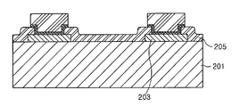
즉, 반도체 공정을 실시하여 반도체(실리콘) 기판(201) 상에 메탈 패드(Metal pad)(203) 및 패시베이션 산화막(passivation Oxide)(205)을 일 예로, 도 2a에 도시된 바와 같이 형성한다. In other words, a semiconductor process may be performed to form a
다음에, 메탈 패드(203) 및 패시베이션 산화막(205) 상부에 베리어 메탈(barrier metal)(TiW)(207)을 전면 증착하고, 이어서 증착된 베리어 메탈(207) 상에 화학 기상 증착(Chemical Vapor Deposition, CVD) 공정을 실시하여 금속(Cu) 씨드(Seed)(209)를 일 예로, 도 2b에 도시된 바와 같이 전면 증착한다. Next, a barrier metal (TiW) 207 is deposited over the
다음으로, 금속(Cu) 씨드(209) 상부에 감광막(Photo Resist, PR)을 전면 증착한 다음에, 전면 증착된 PR의 일부를 Bond pad가 형성될 영역으로 설계된 레티클을 이용하는 노광 공정 및 현상 공정을 실시하여 선택적으로 제거함으로써, 금속 씨드(209) 상부에 본드 패드(Bond Pad)가 형성될 영역을 정의하기 위한 PR 패턴(211)을 일 예로, 도 2c에 도시된 바와 같이 형성한다. Next, an entire surface deposited photoresist (PR) is deposited on the metal (Cu) seed 209, and then an exposure process and a development process using a reticle designed as a region where a bond pad is to be formed on a portion of the front deposited PR. By selectively removing the same, a
이어서, Bond pad가 형성될 영역을 정의하기 위한 PR 패턴(211) 내에 황산 배스(bath)를 사용하는 전기 도금(Electroplating) 공정을 실시하여 금속(213)를 일 예로, 도 2d에 도시된 바와 같이 증착한다. Subsequently, an electroplating process using a sulfuric acid bath in a
마지막으로, 스트리밍 공정을 실시하여 잔류하는 PR 패턴(211)을 제거한 다음에, 이어서 금속 씨드(209)의 일부를 선택적으로 제거하여 일 예로, 도 2e에 도시된 바와 같이 BOAC/COA 제조를 구현할 수 있다. Finally, the
그러나, 상술한 바와 같이 BOAC/COA를 제조함에 있어서, 도 2d의 공정에서와 같이 황산 bath를 사용하는 Electroplating 공정을 실시할 경우, 이 황산 bath에 의해 PR이 녹게 되는 금속 듀얼 다마신(dual damascene) 기법에 위배됨에 따라 금속 증착이 비정상적으로 이루어지며, 또한, 도 2e의 공정에서와 같이 금속 씨드(209)의 일부를 선택적으로 제거하는 스트리밍 공정을 실시할 경우, Bond pad가 형성될 영역에 증착된 물질도 동일한 금속 물질이기 때문에 데미지(Damage)를 받게 되어 반도체 소자의 수율 및 신뢰성을 저하시키게 되는 문제점이 있다. However, in the production of BOAC / COA as described above, when performing an electroplating process using a sulfuric acid bath as in the process of FIG. 2D, the metal dual damascene in which PR is melted by the sulfuric acid bath. Metal deposition is abnormal due to the violation of the technique, and when a streaming process is performed to selectively remove a part of the metal seed 209 as in the process of FIG. Since the materials are the same metal materials, they are damaged, and thus, the yield and reliability of the semiconductor device are reduced.
이에, 본 발명의 기술적 과제는 상술한 문제점을 해결하기 위해 안출한 것으로, 본 발명의 목적은 금속 듀얼 다마신(dual damascene) 공정을 이용하여 BOAC/COA를 구현하여 원가 절감 및 소자 성능을 향상시킬 수 있는 반도체 소자 및 BOAC/COA 제조 방법을 제공함에 있다. Accordingly, the technical problem of the present invention is to solve the above problems, an object of the present invention is to implement a BOAC / COA using a metal dual damascene process to improve the cost reduction and device performance The present invention provides a semiconductor device and a method for manufacturing a BOAC / COA.
상술한 목적을 달성하기 위한 본 발명에서 반도체 소자는 반도체 기판 전면에 형성된 전도성 패드와, 전도성 패드 상에 형성된 패시베이션 산화막과, 전도성 패드 및 패시베이션 산화막 상부에 Bond pad가 형성될 영역으로 정의하기 위해 형성된 금속과, 형성된 금속의 양측벽에 형성된 일부의 베리어막과, 베리어막 양측벽에 형성된 일부의 금속 씨드(Seed)를 포함하는 것을 특징으로 한다. In the present invention for achieving the above object, the semiconductor device is a metal formed to define a conductive pad formed on the front surface of the semiconductor substrate, a passivation oxide film formed on the conductive pad, and a region where the bond pad is formed on the conductive pad and the passivation oxide film And some barrier films formed on both side walls of the formed metal, and some metal seeds formed on both side walls of the barrier film.
상술한 목적을 달성하기 위한 본 발명에서 반도체 소자의 BOAC/COA 제조 방법은 반도체 기판 상에 전도성 패드 및 패시베이션 산화막을 형성하며, 형 성된 전도성 패드 및 패시베이션 산화막 상부에 산화막(Oxide)을 전면 증착하는 단계와, 증착된 산화막의 일부를 선택적으로 제거하여 Bond pad가 형성될 영역을 정의하기 위한 산화막 패턴을 형성하는 단계와, 형성된 산화막 패턴 상부에 베리어막 및 금속 씨드(Seed)를 전면 증착하고, 증착된 금속 씨드 상부에 금속을 전면 증착하고, 증착된 금속에 대하여 산화막 패턴과 일부의 베리어막 및 금속 씨드가 노출될 때까지 평탄화하는 단계와, 노출된 산화막 패턴만을 식각을 통해 제거하여 BOAC/COA를 제조하는 단계를 포함하는 것을 특징으로 한다. In the present invention, a method of manufacturing a COA / COA of a semiconductor device in order to achieve the above object is to form a conductive pad and a passivation oxide film on a semiconductor substrate, and depositing an oxide film on top of the formed conductive pad and passivation oxide film. And selectively removing a portion of the deposited oxide film to form an oxide pattern for defining a region in which a bond pad is to be formed, and depositing a barrier film and a metal seed on the formed oxide film pattern on the entire surface. Full deposition of the metal on the metal seed, and planarization until the oxide pattern, a part of the barrier film and the metal seed is exposed to the deposited metal, and by removing only the exposed oxide pattern through etching to produce a BOAC / COA Characterized in that it comprises a step.
이하, 본 발명의 실시 예는 다수개가 존재할 수 있으며, 이하에서 첨부한 도면을 참조하여 바람직한 실시 예에 대하여 상세히 설명하기로 한다. 이 기술 분야의 숙련자라면 이 실시 예를 통해 본 발명의 목적, 특징 및 이점들을 잘 이해하게 될 것이다. Hereinafter, a plurality of embodiments of the present invention may exist, and a preferred embodiment will be described in detail with reference to the accompanying drawings. Those skilled in the art will appreciate the objects, features and advantages of the present invention through this embodiment.
도 3은 본 발명의 실시 예에 따른 반도체 소자의 BOAC/COA 구조를 나타낸 수직 단면도로서, 다음과 같은 BOAC/COA 구조를 갖는다. 3 is a vertical cross-sectional view illustrating a BOAC / COA structure of a semiconductor device according to an embodiment of the present invention, and has a BOAC / COA structure as follows.
즉, 반도체 기판(401) 상에 메탈 패드(Metal pad)(403) 및 패시베이션 산화막(passivation Oxide)(405)이 형성되어 있다. That is, a
다음으로, 메탈 패드(403) 및 패시베이션 산화막(405) 상부에 Bond pad가 형성될 영역으로 정의하기 위해 금속(Cu)(413)이 형성되어 있다. Next, a metal (Cu) 413 is formed on the
그리고, 금속(Cu)(413) 양측벽에 일부의 베리어 메탈(TiW)(409a)이 형성되어 있으며, 이 형성된 베리어 메탈(409a) 양측벽에 일부의 금속(Cu) 씨드(Seed)(411a)가 형성되어 있다. In addition, some barrier metal (TiW) 409a is formed on both side walls of the metal (Cu) 413, and some metal (Se) seed (411a) is formed on both side walls of the
여기서, Bond pad가 형성될 영역은 산화막(Oxide)을 메탈 패드(403) 및 패시베이션 산화막(405) 상부에 전면 증착시키고, 전면 증착된 산화막의 일부를 선택적으로 제거하여 형성할 수 있다. Here, the region in which the bond pad is to be formed may be formed by depositing an oxide film on the
그리고, 금속(Cu)(413)과 일부 노출된 베리어 메탈(409a) 및 금속(Cu) 씨드(411a)는 산화막 패턴 상부에 베리어 메탈 및 금속(Cu) 씨드를 형성하고, 그 상부에 금속(Cu)(413)을 전면 증착시키며, 증착된 금속(Cu)에 대하여 화학 기계적 연마(Chemical Mechanical Polishing, CMP) 평탄화 공정을 실시하여 산화막 패턴과, 그리고 베리어 메탈(409a) 및 금속 씨드(411a)의 일부가 노출되며, 산화막 식각(Etch)(예컨대, 드라이) 공정을 실시하여 잔류하는 산화막 패턴만을 선택적으로 제거하여 형성할 수 있다. In addition, the metal (Cu) 413 and the
따라서, 본 발명은 금속(Cu) 듀얼 다마신 공정을 이용하여 BOAC/COA를 구현함으로써, 원가 절감 및 소자 성능을 향상시킬 수 있다. Therefore, the present invention can implement a BOAC / COA using a metal (Cu) dual damascene process, it is possible to reduce cost and improve device performance.
도 4a 내지 도 4d는 본 발명의 바람직한 실시 예에 따른 반도체 소자의 BOAC/COA 제조 방법을 설명하기 위한 각 공정별 수직 단면도이다. 4A through 4D are vertical cross-sectional views of respective processes for explaining a method of manufacturing a BOAC / COA of a semiconductor device according to an exemplary embodiment of the present invention.
즉, 반도체 공정을 실시하여 실리콘 기판(401) 상에 전도성(메탈) 패드(403) 및 패시베이션 산화막(405)을 형성하며, 형성된 메탈 패드(403) 및 패시베이션 산화막(405) 상부에 산화막(Oxide)을 전면 증착한 다음에, 전면 증착된 산화막의 일부를 선택적으로 제거함으로써, 메탈 패드(403) 및 패시베이션 산화막(405) 상부에 Bond pad가 형성될 영역을 정의하기 위한 산화막 패턴(407)을 일 예로, 도 3a에 도시된 바와 같이 형성한다. That is, the conductive (metal)
다음에, Bond pad가 형성될 영역을 정의하기 위한 산화막 패턴(407) 상부에 베리어 메탈(베리어막)(409)을 전면 증착하고, 이어서 증착된 베리어 메탈(409) 상에 CVD 공정을 실시하여 금속 씨드(411)를 일 예로, 도 3b에 도시된 바와 같이 전면 증착한다. Next, a barrier metal (barrier film) 409 is entirely deposited on the
다음으로, 금속 씨드(411) 상부에 금속(413)을 전면 증착한 다음에, 증착된 금속에 대하여 CMP 공정을 실시하여 일 예로, 도 3c에 도시된 바와 같이 산화막 패턴(407a)과 그리고 베리어 메탈(409a) 및 금속 씨드(411a)가 일부 노출될 때까지 평탄화한다. Next, the entire surface of the
마지막으로, 산화막 식각(Etch)(드라이) 공정을 실시하여 잔류하는 산화막 패턴(407a)만을 선택적으로 제거하면 금속(413)과, 그리고 일부 노출된 베리어 메탈(409a) 및 금속 씨드(411a)는 제거되지 않으면서 일 예로, 도 3d에 도시된 바와 같이 BOAC/COA 제조를 구현할 수 있다. Finally, if only the
따라서, 본 발명은 금속(Cu) 듀얼 다마신 공정을 이용하여 BOAC/COA를 구현함으로써, 기존에서와 같이 황산 bath에 의해 PR이 녹게 되어 금속 증착이 비정상적으로 이루어지는 문제점과, 그리고 스트리밍 공정에서 동일한 금속 물질에 의해 데미지(Damage)가 발생되는 문제점을 해결할 수 있어 반도체 소자의 수율 및 신뢰성을 향상시킬 수 있다. Accordingly, the present invention implements BOAC / COA using a metal (Cu) dual damascene process, so that the PR is melted by a sulfuric acid bath as in the prior art, so that the metal deposition is abnormal, and the same metal in the streaming process. It is possible to solve the problem of damage caused by the material, thereby improving the yield and reliability of the semiconductor device.
또한, 본 발명의 사상 및 특허청구범위 내에서 권리로서 개시하고 있으므로, 본원 발명은 일반적인 원리들을 이용한 임의의 변형, 이용 및/또는 개작을 포함할 수도 있으며, 본 명세서의 설명으로부터 벗어나는 사항으로서 본 발명이 속하는 업 계에서 공지 또는 관습적 실시의 범위에 해당하고 또한 첨부된 특허청구범위의 제한 범위 내에 포함되는 모든 사항을 포함한다. In addition, since the present invention is disclosed as a right within the spirit and claims of the present invention, the present invention may include any modification, use and / or adaptation using general principles, and the present invention as a matter deviating from the description of the present specification. It includes all matters falling within the scope of the known or customary practice in the industry and falling within the scope of the appended claims.
상기에서 설명한 바와 같이, 본 발명은 금속 듀얼 다마신 공정을 이용하여 BOAC/COA를 구현함으로써, 기존에서와 같이 황산 bath에 의해 PR이 녹게 되어 금속 증착이 비정상적으로 이루어지는 문제점과, 그리고 스트리밍 공정에서 동일한 금속 물질에 의해 데미지가 발생되는 문제점을 해결할 수 있어 반도체 소자의 수율 및 신뢰성을 향상시킬 수 있다. As described above, the present invention implements the BOAC / COA using a metal dual damascene process, so that the PR is melted by a sulfuric acid bath as in the past, the metal deposition is abnormal, and the same in the streaming process It is possible to solve the problem of damage caused by the metal material, thereby improving the yield and reliability of the semiconductor device.
또한, 본 발명은 반도체 소자의 수율 및 신뢰성이 향상되어 원가 절감 및 소자 성능을 향상시킬 수 있는 효과가 있다. In addition, the present invention has the effect of improving the yield and reliability of the semiconductor device to reduce the cost and device performance.
Claims (9)
Priority Applications (4)
| Application Number | Priority Date | Filing Date | Title |
|---|---|---|---|
| KR1020070048576A KR100871768B1 (en) | 2007-05-18 | 2007-05-18 | Semiconductor element and COA / COA manufacturing method |
| US12/120,943 US20080284023A1 (en) | 2007-05-18 | 2008-05-15 | Semiconductor device and method for manufacturing boac/coa |
| TW097118271A TW200849433A (en) | 2007-05-18 | 2008-05-16 | Semiconductor device and method for manufacturing BOAC/COA |
| CN2008100947595A CN101308829B (en) | 2007-05-18 | 2008-05-16 | Semiconductor device and method for manufacturing BOAC/COA |
Applications Claiming Priority (1)
| Application Number | Priority Date | Filing Date | Title |
|---|---|---|---|
| KR1020070048576A KR100871768B1 (en) | 2007-05-18 | 2007-05-18 | Semiconductor element and COA / COA manufacturing method |
Publications (2)
| Publication Number | Publication Date |
|---|---|
| KR20080101446A KR20080101446A (en) | 2008-11-21 |
| KR100871768B1 true KR100871768B1 (en) | 2008-12-05 |
Family
ID=40026700
Family Applications (1)
| Application Number | Title | Priority Date | Filing Date |
|---|---|---|---|
| KR1020070048576A Expired - Fee Related KR100871768B1 (en) | 2007-05-18 | 2007-05-18 | Semiconductor element and COA / COA manufacturing method |
Country Status (4)
| Country | Link |
|---|---|
| US (1) | US20080284023A1 (en) |
| KR (1) | KR100871768B1 (en) |
| CN (1) | CN101308829B (en) |
| TW (1) | TW200849433A (en) |
Families Citing this family (5)
| Publication number | Priority date | Publication date | Assignee | Title |
|---|---|---|---|---|
| KR101313690B1 (en) * | 2011-12-30 | 2013-10-02 | 주식회사 동부하이텍 | Method for fabricating bonding structure of semiconductor device |
| US10037957B2 (en) * | 2016-11-14 | 2018-07-31 | Amkor Technology, Inc. | Semiconductor device and method of manufacturing thereof |
| KR102492733B1 (en) | 2017-09-29 | 2023-01-27 | 삼성디스플레이 주식회사 | Copper plasma etching method and manufacturing method of display panel |
| US11024344B2 (en) | 2018-10-09 | 2021-06-01 | International Business Machines Corporation | Landing pad in interconnect and memory stacks: structure and formation of the same |
| CN114582745B (en) * | 2022-03-07 | 2026-01-20 | 厦门市三安集成电路有限公司 | HBT device and preparation method thereof |
Citations (2)
| Publication number | Priority date | Publication date | Assignee | Title |
|---|---|---|---|---|
| JPH11186309A (en) | 1997-12-19 | 1999-07-09 | Sony Corp | Semiconductor device and method of manufacturing semiconductor device |
| JP2005210121A (en) | 2004-01-22 | 2005-08-04 | Internatl Business Mach Corp <Ibm> | Integration of bonding pads and high performance copper inductors |
Family Cites Families (17)
| Publication number | Priority date | Publication date | Assignee | Title |
|---|---|---|---|---|
| US5953626A (en) * | 1996-06-05 | 1999-09-14 | Advanced Micro Devices, Inc. | Dissolvable dielectric method |
| KR100385042B1 (en) * | 1998-12-03 | 2003-06-18 | 인터내셔널 비지네스 머신즈 코포레이션 | Method for forming electromigration-resistant structures by doping |
| US7381642B2 (en) * | 2004-09-23 | 2008-06-03 | Megica Corporation | Top layers of metal for integrated circuits |
| US6500750B1 (en) * | 1999-04-05 | 2002-12-31 | Motorola, Inc. | Semiconductor device and method of formation |
| US6355153B1 (en) * | 1999-09-17 | 2002-03-12 | Nutool, Inc. | Chip interconnect and packaging deposition methods and structures |
| US6252290B1 (en) * | 1999-10-25 | 2001-06-26 | Chartered Semiconductor Manufacturing Ltd. | Method to form, and structure of, a dual damascene interconnect device |
| US6458683B1 (en) * | 2001-03-30 | 2002-10-01 | Taiwan Semiconductor Manufacturing Co., Ltd | Method for forming aluminum bumps by CVD and wet etch |
| KR100499557B1 (en) * | 2001-06-11 | 2005-07-07 | 주식회사 하이닉스반도체 | method for fabricating the wire of semiconductor device |
| US6403461B1 (en) * | 2001-07-25 | 2002-06-11 | Chartered Semiconductor Manufacturing Ltd. | Method to reduce capacitance between metal lines |
| US6593220B1 (en) * | 2002-01-03 | 2003-07-15 | Taiwan Semiconductor Manufacturing Company | Elastomer plating mask sealed wafer level package method |
| US6717265B1 (en) * | 2002-11-08 | 2004-04-06 | Intel Corporation | Treatment of low-k dielectric material for CMP |
| US7144490B2 (en) * | 2003-11-18 | 2006-12-05 | International Business Machines Corporation | Method for selective electroplating of semiconductor device I/O pads using a titanium-tungsten seed layer |
| KR100583957B1 (en) * | 2003-12-03 | 2006-05-26 | 삼성전자주식회사 | Method of forming double damascene metal wiring by adopting sacrificial metal oxide film |
| US6995084B2 (en) * | 2004-03-17 | 2006-02-07 | International Business Machines Corporation | Method for forming robust solder interconnect structures by reducing effects of seed layer underetching |
| KR100819557B1 (en) * | 2006-08-17 | 2008-04-07 | 삼성전자주식회사 | Metal etching solution, metal etching method using same, and method of manufacturing semiconductor product using same |
| US7582966B2 (en) * | 2006-09-06 | 2009-09-01 | Megica Corporation | Semiconductor chip and method for fabricating the same |
| US7800239B2 (en) * | 2007-12-14 | 2010-09-21 | Semiconductor Components Industries, Llc | Thick metal interconnect with metal pad caps at selective sites and process for making the same |
-
2007
- 2007-05-18 KR KR1020070048576A patent/KR100871768B1/en not_active Expired - Fee Related
-
2008
- 2008-05-15 US US12/120,943 patent/US20080284023A1/en not_active Abandoned
- 2008-05-16 TW TW097118271A patent/TW200849433A/en unknown
- 2008-05-16 CN CN2008100947595A patent/CN101308829B/en not_active Expired - Fee Related
Patent Citations (2)
| Publication number | Priority date | Publication date | Assignee | Title |
|---|---|---|---|---|
| JPH11186309A (en) | 1997-12-19 | 1999-07-09 | Sony Corp | Semiconductor device and method of manufacturing semiconductor device |
| JP2005210121A (en) | 2004-01-22 | 2005-08-04 | Internatl Business Mach Corp <Ibm> | Integration of bonding pads and high performance copper inductors |
Also Published As
| Publication number | Publication date |
|---|---|
| KR20080101446A (en) | 2008-11-21 |
| TW200849433A (en) | 2008-12-16 |
| CN101308829A (en) | 2008-11-19 |
| US20080284023A1 (en) | 2008-11-20 |
| CN101308829B (en) | 2010-06-02 |
Similar Documents
| Publication | Publication Date | Title |
|---|---|---|
| US12381195B2 (en) | Semiconductor devices and methods of manufacture thereof | |
| CN101714539B (en) | The Z-shaped structure of adhering to for TSV copper | |
| US20120228778A1 (en) | Substrates with through vias with conductive features for connection to integrated circuit elements, and methods for forming through vias in substrates | |
| TWI685938B (en) | Skip via structures | |
| JP2006344703A5 (en) | ||
| US10692733B2 (en) | Uniform back side exposure of through-silicon vias | |
| TWI713093B (en) | Semiconductor device having passivation layer and method of making the same | |
| KR100871768B1 (en) | Semiconductor element and COA / COA manufacturing method | |
| KR101701573B1 (en) | Bi-layer hard mask for robust metalization profile | |
| CN103247598B (en) | Hard mask is adopted to form metal wire and through hole | |
| JP5891753B2 (en) | Manufacturing method of semiconductor device | |
| CN114141698B (en) | Semiconductor structure and method for manufacturing the same | |
| KR101976727B1 (en) | Method for forming interconnection structures | |
| CN109887880B (en) | A kind of semiconductor connection structure and its manufacturing method | |
| CN108231599B (en) | Method for improving flat uniformity of wafer surface | |
| KR100447977B1 (en) | Method for forming metal line of semiconductor device by using dual damascene process | |
| US20240321723A1 (en) | Structure to mitigate vertical interconnect access induced metal corrosion | |
| KR20090124398A (en) | Semiconductor device manufacturing method | |
| US20160211405A1 (en) | Method of manufacturing semiconductor device | |
| US20120090648A1 (en) | Cleaning method for semiconductor wafer and cleaning device for semiconductor wafer | |
| KR101010848B1 (en) | Metal wiring manufacturing method and metal wiring of semiconductor device | |
| JP2007287731A (en) | Manufacturing method of semiconductor device |
Legal Events
| Date | Code | Title | Description |
|---|---|---|---|
| A201 | Request for examination | ||
| PA0109 | Patent application |
St.27 status event code: A-0-1-A10-A12-nap-PA0109 |
|
| PA0201 | Request for examination |
St.27 status event code: A-1-2-D10-D11-exm-PA0201 |
|
| PN2301 | Change of applicant |
St.27 status event code: A-3-3-R10-R13-asn-PN2301 St.27 status event code: A-3-3-R10-R11-asn-PN2301 |
|
| D13-X000 | Search requested |
St.27 status event code: A-1-2-D10-D13-srh-X000 |
|
| D14-X000 | Search report completed |
St.27 status event code: A-1-2-D10-D14-srh-X000 |
|
| E902 | Notification of reason for refusal | ||
| PE0902 | Notice of grounds for rejection |
St.27 status event code: A-1-2-D10-D21-exm-PE0902 |
|
| E13-X000 | Pre-grant limitation requested |
St.27 status event code: A-2-3-E10-E13-lim-X000 |
|
| P11-X000 | Amendment of application requested |
St.27 status event code: A-2-2-P10-P11-nap-X000 |
|
| P13-X000 | Application amended |
St.27 status event code: A-2-2-P10-P13-nap-X000 |
|
| E701 | Decision to grant or registration of patent right | ||
| PE0701 | Decision of registration |
St.27 status event code: A-1-2-D10-D22-exm-PE0701 |
|
| PG1501 | Laying open of application |
St.27 status event code: A-1-1-Q10-Q12-nap-PG1501 |
|
| GRNT | Written decision to grant | ||
| PR0701 | Registration of establishment |
St.27 status event code: A-2-4-F10-F11-exm-PR0701 |
|
| PR1002 | Payment of registration fee |
St.27 status event code: A-2-2-U10-U11-oth-PR1002 Fee payment year number: 1 |
|
| PG1601 | Publication of registration |
St.27 status event code: A-4-4-Q10-Q13-nap-PG1601 |
|
| FPAY | Annual fee payment |
Payment date: 20111020 Year of fee payment: 4 |
|
| PR1001 | Payment of annual fee |
St.27 status event code: A-4-4-U10-U11-oth-PR1001 Fee payment year number: 4 |
|
| FPAY | Annual fee payment |
Payment date: 20121026 Year of fee payment: 5 |
|
| PR1001 | Payment of annual fee |
St.27 status event code: A-4-4-U10-U11-oth-PR1001 Fee payment year number: 5 |
|
| LAPS | Lapse due to unpaid annual fee | ||
| PC1903 | Unpaid annual fee |
St.27 status event code: A-4-4-U10-U13-oth-PC1903 Not in force date: 20131127 Payment event data comment text: Termination Category : DEFAULT_OF_REGISTRATION_FEE |
|
| PC1903 | Unpaid annual fee |
St.27 status event code: N-4-6-H10-H13-oth-PC1903 Ip right cessation event data comment text: Termination Category : DEFAULT_OF_REGISTRATION_FEE Not in force date: 20131127 |
|
| PN2301 | Change of applicant |
St.27 status event code: A-5-5-R10-R13-asn-PN2301 St.27 status event code: A-5-5-R10-R11-asn-PN2301 |
|
| R18-X000 | Changes to party contact information recorded |
St.27 status event code: A-5-5-R10-R18-oth-X000 |
|
| P22-X000 | Classification modified |
St.27 status event code: A-4-4-P10-P22-nap-X000 |