KR100846393B1 - Transistor of semiconductor device and manufacturing method thereof - Google Patents
Transistor of semiconductor device and manufacturing method thereof Download PDFInfo
- Publication number
- KR100846393B1 KR100846393B1 KR1020070031720A KR20070031720A KR100846393B1 KR 100846393 B1 KR100846393 B1 KR 100846393B1 KR 1020070031720 A KR1020070031720 A KR 1020070031720A KR 20070031720 A KR20070031720 A KR 20070031720A KR 100846393 B1 KR100846393 B1 KR 100846393B1
- Authority
- KR
- South Korea
- Prior art keywords
- gate
- transistor
- pattern
- gate pattern
- spacer
- Prior art date
- Legal status (The legal status is an assumption and is not a legal conclusion. Google has not performed a legal analysis and makes no representation as to the accuracy of the status listed.)
- Expired - Fee Related
Links
Images


Classifications
-
- H—ELECTRICITY
- H10—SEMICONDUCTOR DEVICES; ELECTRIC SOLID-STATE DEVICES NOT OTHERWISE PROVIDED FOR
- H10D—INORGANIC ELECTRIC SEMICONDUCTOR DEVICES
- H10D30/00—Field-effect transistors [FET]
- H10D30/01—Manufacture or treatment
- H10D30/021—Manufacture or treatment of FETs having insulated gates [IGFET]
- H10D30/023—Manufacture or treatment of FETs having insulated gates [IGFET] having multiple independently-addressable gate electrodes influencing the same channel
-
- H—ELECTRICITY
- H10—SEMICONDUCTOR DEVICES; ELECTRIC SOLID-STATE DEVICES NOT OTHERWISE PROVIDED FOR
- H10D—INORGANIC ELECTRIC SEMICONDUCTOR DEVICES
- H10D30/00—Field-effect transistors [FET]
- H10D30/60—Insulated-gate field-effect transistors [IGFET]
- H10D30/601—Insulated-gate field-effect transistors [IGFET] having lightly-doped drain or source extensions, e.g. LDD IGFETs or DDD IGFETs
-
- H—ELECTRICITY
- H10—SEMICONDUCTOR DEVICES; ELECTRIC SOLID-STATE DEVICES NOT OTHERWISE PROVIDED FOR
- H10D—INORGANIC ELECTRIC SEMICONDUCTOR DEVICES
- H10D30/00—Field-effect transistors [FET]
- H10D30/60—Insulated-gate field-effect transistors [IGFET]
- H10D30/611—Insulated-gate field-effect transistors [IGFET] having multiple independently-addressable gate electrodes influencing the same channel
-
- H—ELECTRICITY
- H10—SEMICONDUCTOR DEVICES; ELECTRIC SOLID-STATE DEVICES NOT OTHERWISE PROVIDED FOR
- H10D—INORGANIC ELECTRIC SEMICONDUCTOR DEVICES
- H10D64/00—Electrodes of devices having potential barriers
- H10D64/20—Electrodes characterised by their shapes, relative sizes or dispositions
- H10D64/27—Electrodes not carrying the current to be rectified, amplified, oscillated or switched, e.g. gates
- H10D64/311—Gate electrodes for field-effect devices
- H10D64/411—Gate electrodes for field-effect devices for FETs
- H10D64/511—Gate electrodes for field-effect devices for FETs for IGFETs
- H10D64/517—Gate electrodes for field-effect devices for FETs for IGFETs characterised by the conducting layers
- H10D64/518—Gate electrodes for field-effect devices for FETs for IGFETs characterised by the conducting layers characterised by their lengths or sectional shapes
Landscapes
- Metal-Oxide And Bipolar Metal-Oxide Semiconductor Integrated Circuits (AREA)
- Insulated Gate Type Field-Effect Transistor (AREA)
- Electrodes Of Semiconductors (AREA)
- Semiconductor Memories (AREA)
Abstract
본 발명은 반도체 소자의 트랜지스터 및 그 제조 방법에 관한 것으로, 본 발명의 트랜지스터는 반도체 기판상에 형성되고 제1 게이트 전극 및 제1 게이트 하드마스크가 적층된 구조를 갖는 제1 게이트 패턴; 상기 제1 게이트 패턴 측벽에 형성된 제1 게이트 스페이서; 상기 제1 게이트 패턴 및 상기 제1 게이트 스페이서의 양측면과 상부면을 감싸면서 제2 게이트 전극 및 제2 게이트 하드마스크가 적층된 구조를 갖는 제2 게이트 패턴; 및 상기 제2 게이트 패턴 측벽의 제2 게이트 스페이서를 포함하고, 상술한 본 발명에 의한 반도체 소자의 트랜지스터 및 그 제조 방법은 제1 게이트 패턴과 제1 게이트 패턴을 감싸는 제2 게이트 패턴으로 이루어진 더블 게이트 구조의 트랜지스터를 제조함으로써, 트랜지스터의 형성 면적과 누설 전류를 감소시킬 수 있고 아울러 고속 동작을 가능하게 한다.The present invention relates to a transistor of a semiconductor device and a method of manufacturing the same, the transistor of the present invention comprises: a first gate pattern formed on a semiconductor substrate and having a structure in which a first gate electrode and a first gate hard mask are stacked; A first gate spacer formed on sidewalls of the first gate pattern; A second gate pattern having a structure in which a second gate electrode and a second gate hard mask are stacked while covering the first gate pattern and both side surfaces and the top surface of the first gate spacer; And a second gate spacer on the sidewalls of the second gate pattern, wherein the semiconductor device transistor and the method of manufacturing the same according to the present invention include a double gate including a first gate pattern and a second gate pattern surrounding the first gate pattern. By manufacturing the transistor of the structure, it is possible to reduce the formation area and the leakage current of the transistor and to enable high speed operation.
Description
도1a 내지 도1c는 종래 기술에 따른 더블 게이트 구조를 갖는 트랜지스터를 설명하기 위한 도면.1A to 1C are diagrams for explaining a transistor having a double gate structure according to the prior art;
도2a 내지 도2c는 본 발명의 일실시예에 따른 반도체 소자의 트랜지스터를 설명하기 위한 도면.2A to 2C are diagrams for describing a transistor of a semiconductor device according to an embodiment of the present invention.
도3a 내지 도3d는 본 발명의 일실시예에 따른 반도체 소자의 트랜지스터 제조 방법을 설명하기 위한 공정 단면도.3A to 3D are cross-sectional views illustrating a method of manufacturing a transistor of a semiconductor device in accordance with an embodiment of the present invention.
* 도면의 주요 부분에 대한 부호의 설명* Explanation of symbols for the main parts of the drawings
201 : 반도체 기판 203 : 소자 분리막201: semiconductor substrate 203: device isolation film
205 : 제1 게이트 절연막 207 : 제1 폴리실리콘막205: first gate insulating film 207: first polysilicon film
209 : 제1 텅스텐 실리사이드막 211 : 제1 질화막209: first tungsten silicide film 211: first nitride film
213 : 제1 게이트 스페이서 215 : 제2 게이트 절연막213: first gate spacer 215: second gate insulating film
217 : 제2 폴리실리콘막 219 : 제2 텅스텐 실리사이드막217: second polysilicon film 219: second tungsten silicide film
221 : 제2 질화막 223 : 제2 게이트 스페이서221: second nitride film 223: second gate spacer
20 : 제1 게이트 패턴 21 : 제2 게이트 패턴20: first gate pattern 21: second gate pattern
본 발명은 반도체 소자의 제조 기술에 관한 것으로, 특히 반도체 소자의 트랜지스터 및 그 제조 방법에 관한 것이다.BACKGROUND OF THE INVENTION 1. Field of the Invention The present invention relates to a semiconductor device manufacturing technology, and more particularly, to a transistor of a semiconductor device and a method of manufacturing the same.
종래 기술에 따르면 반도체 소자의 트랜지스터는 반도체 기판의 활성영역을 가로지르는 한 개의 게이트 패턴을 갖는 싱글 게이트(single gate) 구조를 가질 수 있다. 이러한 싱글 게이트 구조를 이용하는 경우, 트랜지스터의 형성 면적을 줄일 수 있는 이점이 있으나, 트랜지스터의 누설 전류 특성과 턴온 전류 특성을 동시에 만족시키기는 어렵다. 이는, 트랜지스터의 누설 전류 특성과 턴온 전류 특성이 상호 트레이드 오프(trade off) 관계에 있기 때문이다. 따라서, 낮은 소비 전력을 갖는 고속 트랜지스터의 형성이 어렵다.According to the prior art, the transistor of the semiconductor device may have a single gate structure having one gate pattern crossing the active region of the semiconductor substrate. In the case of using such a single gate structure, there is an advantage in that the transistor formation area can be reduced, but it is difficult to simultaneously satisfy the leakage current characteristic and the turn-on current characteristic of the transistor. This is because the leakage current characteristic and the turn-on current characteristic of the transistor are in a trade off relationship with each other. Therefore, it is difficult to form a high speed transistor having low power consumption.
이러한 문제를 해결하기 위하여, 트랜지스터의 턴온 전류 특성을 유지시키면서도 누설 전류 특성을 감소시킬 수 있는 더블 게이트(double gate) 구조를 갖는 트랜지스터가 제안되었다. In order to solve this problem, a transistor having a double gate structure capable of reducing leakage current characteristics while maintaining turn-on current characteristics of the transistor has been proposed.
도1a 내지 도1c는 종래 기술에 따른 더블 게이트 구조를 갖는 트랜지스터를 설명하기 위한 도면이다. 도1a는 종래 기술에 따른 더블 게이트 구조를 갖는 트랜지스터의 레이아웃 도면이고, 도1b는 도1a의 I-I´ 단면도이며, 도1c는 도1a의 등 가 회로도이다.1A to 1C are diagrams for describing a transistor having a double gate structure according to the related art. FIG. 1A is a layout diagram of a transistor having a double gate structure according to the prior art, FIG. 1B is a sectional view taken along line II ′ of FIG. 1A, and FIG. 1C is an equivalent circuit diagram of FIG. 1A.
도1a 내지 도1c를 참조하면, 반도체 기판(101)의 소자 분리 영역(F)에 형성된 소자 분리막(103)에 의해 활성 영역(A)이 한정된다.1A to 1C, the active region A is defined by the
반도체 기판(101)의 활성영역(A) 상에는 활성영역(A)을 가로지르는 두 개의 게이트 패턴 즉, 제1 및 제2 게이트 패턴(105, 107)이 소정 거리 이격되어 형성된다. 이와 같이 활성영역 상에 두 개의 게이트가 형성된 구조를 더블 게이트 구조라 한다.On the active region A of the
제1 게이트 패턴(105)과 제2 게이트 패턴(107) 양측의 반도체 기판(101) 내에는 소스/드레인 접합 영역(미도시됨)이 형성된다. 도1a의 레이아웃 도면을 참조하면, 이러한 소스/드레인 접합 영역은 소정 간격으로 이격된 복수개의 소스/드레인 콘택(C)을 통하여 후속 비트라인 또는 스토리지 전극과 연결된다.Source / drain junction regions (not shown) are formed in the
전술한 더블 게이트 구조를 갖는 트랜지스터는 싱글 게이트 구조를 갖는 트랜지스터에 비하여 게이트를 하나 더 갖고 있기 때문에 누설 전류 특성이 개선되는 이점을 가지나, 트랜지스터가 차지하는 면적이 증가하여 최근 급격히 증가되고 있는 반도체 소자의 고집적화 요구를 만족시킬 수 없다.The transistor having the double gate structure described above has an advantage of improving leakage current characteristics since it has one more gate as compared to the transistor having a single gate structure, but the high integration of the semiconductor device, which has recently increased rapidly due to the increased area of the transistor, has increased. Can't satisfy the demand
본 발명은 상기한 종래기술의 문제점을 해결하기 위하여 제안된 것으로, 제1 게이트 패턴과 제1 게이트 패턴을 감싸는 제2 게이트 패턴으로 이루어진 더블 게이트 구조의 트랜지스터를 제조함으로써, 트랜지스터의 형성 면적과 누설 전류를 감 소시킬 수 있고 아울러 고속 동작을 가능하게 하는 반도체 소자의 트랜지스터 및 그 제조 방법을 제공하는데 그 목적이 있다.The present invention has been proposed to solve the above problems of the prior art, and by manufacturing a transistor having a double gate structure consisting of a first gate pattern and a second gate pattern surrounding the first gate pattern, the transistor formation area and leakage current It is an object of the present invention to provide a transistor of a semiconductor device and a method of manufacturing the same, which can reduce the number and enable high-speed operation.
상기 목적을 달성하기 위한 본 발명의 트랜지스터는, 반도체 기판상에 형성되고 제1 게이트 전극 및 제1 게이트 하드마스크가 적층된 구조를 갖는 제1 게이트 패턴; 상기 제1 게이트 패턴 측벽에 형성된 제1 게이트 스페이서; 상기 제1 게이트 패턴 및 상기 제1 게이트 스페이서의 양측면과 상부면을 감싸면서 제2 게이트 전극 및 제2 게이트 하드마스크가 적층된 구조를 갖는 제2 게이트 패턴; 및 상기 제2 게이트 패턴 측벽의 제2 게이트 스페이서를 포함한다.A transistor of the present invention for achieving the above object comprises a first gate pattern formed on a semiconductor substrate and having a structure in which a first gate electrode and a first gate hard mask are stacked; A first gate spacer formed on sidewalls of the first gate pattern; A second gate pattern having a structure in which a second gate electrode and a second gate hard mask are stacked while covering the first gate pattern and both side surfaces and the top surface of the first gate spacer; And a second gate spacer on the sidewall of the second gate pattern.
또한, 상기 목적을 달성하기 위한 본 발명의 트랜지스터 제조 방법은, 반도체 기판상에 제1 게이트 절연막을 형성하는 단계; 상기 제1 게이트 절연막 상에 제1 게이트 전극 및 제1 게이트 하드마스크가 적층된 구조의 제1 게이트 패턴을 형성하는 단계; 상기 제1 게이트 패턴 측벽에 제1 게이트 스페이서를 형성하는 단계; 상기 제1 게이트 패턴 및 상기 제1 게이트 스페이서를 포함하는 결과물의 전면에 제2 게이트 절연막을 형성하는 단계; 상기 제2 게이트 절연막 상에 상기 제1 게이트 패턴 및 상기 제1 게이트 스페이서의 양측면 및 상부면을 감싸면서 제2 게이트 전극 및 제2 게이트 하드마스크가 적층된 구조를 갖는 제2 게이트 패턴을 형성하는 단계; 및 상기 제2 게이트 패턴 측벽에 제2 게이트 스페이서를 형성하는 단계를 포함한다.In addition, the transistor manufacturing method of the present invention for achieving the above object comprises the steps of forming a first gate insulating film on a semiconductor substrate; Forming a first gate pattern having a structure in which a first gate electrode and a first gate hard mask are stacked on the first gate insulating layer; Forming a first gate spacer on sidewalls of the first gate pattern; Forming a second gate insulating film on an entire surface of the resultant product including the first gate pattern and the first gate spacer; Forming a second gate pattern having a structure in which a second gate electrode and a second gate hard mask are stacked on the second gate insulating layer to surround both side surfaces and upper surfaces of the first gate pattern and the first gate spacer; ; And forming a second gate spacer on sidewalls of the second gate pattern.
또한, 상기 목적을 달성하기 위한 본 발명의 트랜지스터 레이아웃 구조는, 활성 영역을 가로지르는 방향으로 형성된 제1 게이트; 상기 제1 게이트와 중첩되면서 상기 제1 게이트보다 큰 폭을 갖는 제2 게이트; 및 상기 제1 게이트 및 상기 제2 게이트를 중심으로 양 측에 배치된 소스/드레인 콘택을 포함한다.In addition, the transistor layout structure of the present invention for achieving the above object comprises a first gate formed in a direction crossing the active region; A second gate overlapping the first gate and having a width greater than that of the first gate; And source / drain contacts disposed at both sides of the first gate and the second gate.
이하, 본 발명이 속하는 기술 분야에서 통상의 지식을 가진 자가 본 발명의 기술적 사상을 용이하게 실시할 수 있을 정도로 상세히 설명하기 위하여, 본 발명의 가장 바람직한 실시예를 첨부된 도면을 참조하여 설명하기로 한다.DETAILED DESCRIPTION Hereinafter, the most preferred embodiments of the present invention will be described with reference to the accompanying drawings so that those skilled in the art may easily implement the technical idea of the present invention. do.
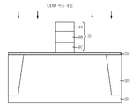
도2a 내지 도2c는 본 발명의 일실시예에 따른 반도체 소자의 트랜지스터를 설명하기 위한 도면이다. 도2a는 본 발명의 일실시예에 따른 트랜지스터의 레이아웃 도면이고, 도2b는 도2a의 Ⅱ-Ⅱ´ 단면도이며, 도2c는 도2a의 등가 회로도이다.2A to 2C are diagrams for describing a transistor of a semiconductor device according to an embodiment of the present invention. FIG. 2A is a layout diagram of a transistor according to an embodiment of the present invention, FIG. 2B is a sectional view taken along line II-II ′ of FIG. 2A, and FIG. 2C is an equivalent circuit diagram of FIG. 2A.
도2a 내지 도2c를 참조하면, 반도체 기판(201)의 소자 분리 영역(F)에 형성된 소자 분리막(203)에 의해 반도체 기판(201)의 활성 영역(A)이 한정된다.2A to 2C, the active region A of the
반도체 기판(201)의 활성영역(A) 상에는 활성영역(A)을 가로지르는 두 개의 게이트 패턴 즉, 제1 및 제2 게이트 패턴(20, 21)이 적층된 구조로 형성된다. 이때, 제2 게이트 패턴(21)은 제1 게이트 패턴(20)의 양측벽 및 상부면을 감싸도록 제1 게이트 패턴(20) 상에서 제1 게이트 패턴(20)보다 더 큰 폭을 갖도록 형성된다.On the active region A of the
좀더 상세하게는, 제1 게이트 패턴(20)은 제1 게이트 절연막(205)에 의해 반도체 기판(201)과 절연되며, 게이트 전극용 제1 폴리실리콘막(207), 게이트 전극용 제1 텅스텐 실리사이드막(209) 및 게이트 하드마스크용 제1 질화막(211)이 순차적으로 적층된 구조를 갖는다. 제1 게이트 패턴(20)의 측벽에는 질화막으로 이루어진 제1 게이트 스페이서(213)가 형성된다. 이때, 제1 질화막(211) 및 제1 게이트 스페이서(213)는 제2 게이트 패턴(21)과의 분리막으로 작용한다. 제1 질화막(211)은 10nm 정도의 두께로 형성됨이 바람직하고, 제1 게이트 스페이서(213)은 5nm의 두께로 형성됨이 바람직하다.More specifically, the
또한, 제2 게이트 패턴(21)은 제2 게이트 절연막(215)에 의해서 반도체 기판(201)과 절연되며, 게이트 전극용 제2 폴리실리콘막(217), 게이트 전극용 제2 텅스텐 실리사이드막(219) 및 게이트 하드마스크용 제2 질화막(221)이 순차적으로 적층된 구조를 갖는다. 제2 게이트 패턴(22)의 측벽에는 질화막으로 이루어진 제2 게이트 스페이서(223)가 형성된다. 여기서, 전술한 바와 같이 제2 게이트 패턴(21)이 제1 게이트 패턴(20)의 양측벽 및 상부면을 감싸기 위해서는, 제2 게이트 패턴(21)의 폭이 제1 게이트 패턴(20)의 폭보다 커야 하며 제2 게이트 패턴(21)을 구성하는 가장 하부막인 게이트 전극용 제2 폴리실리콘막(217)의 높이가 적어도 제1 게이트 패턴(20)의 높이보다 높은 것이 바람직하다. In addition, the
제1 게이트 패턴(20) 양측의 반도체 기판(201) 내에는 LDD 이온 주입 영역(미도시됨)이 형성되고 제2 게이트 패턴(21) 양측의 반도체 기판(201) 내에는 소스/드레인 접합 영역(미도시됨)이 형성된다. 도2a의 레이아웃 도면을 참조하면, 이러한 소스/드레인 접합 영역은 소정 간격으로 이격된 복수개의 소스/드레인 콘택(C)을 통하여 후속 비트라인 또는 스토리지 전극과 연결된다.LDD ion implantation regions (not shown) are formed in the
이와 같은 더블 게이트 구조를 갖는 트랜지스터는 2개의 게이트를 적층 구조로 형성하여 종래 기술의 더블 게이트 구조를 갖는 트랜지스터에 비하여 트랜지스터 형성 면적을 감소시킬 수 있고, 그에 따라 반도체 소자의 고집적화 요구를 만족시킬 수 있다. 아울러, 본 발명의 더블 게이트 구조를 갖는 트랜지스터는 스탠바이(stand-by) 모드에서 2개의 게이트를 모두 턴오프(turn off) 상태로 두어 누설 전류가 감소되고, 액티브(active) 모드에서는 1개의 게이트을 항상 턴온(turn on) 상태로 두어 고속 동작이 가능하다.Such a transistor having a double gate structure can reduce the transistor formation area compared to a transistor having a double gate structure by forming two gates in a stacked structure, thereby satisfying the high integration requirements of the semiconductor device. . In addition, in the transistor having the double gate structure of the present invention, both gates are turned off in the stand-by mode to reduce the leakage current, and one gate is always in the active mode. High speed operation is possible by leaving it on.
도3a 내지 도3d는 본 발명의 일실시예에 따른 반도체 소자의 트랜지스터 제조 방법을 설명하기 위한 공정 단면도이다.3A to 3D are cross-sectional views illustrating a method of manufacturing a transistor of a semiconductor device according to an embodiment of the present invention.
도3a에 도시된 바와 같이, 반도체 기판(301)의 소자 분리 영역에 소자간 격리를 위한 소자 분리막(303)을 형성하여 활성 영역을 한정한 후, 활성 영역에 웰(well) 형성을 위한 이온주입을 수행한다.As shown in FIG. 3A, after forming an
이어서, 반도체 기판(301) 상에 제1 게이트 절연막(305)을 형성한 후, 제1 게이트 절연막(305) 상에 게이트 전극용 도전막으로 제1 폴리실리콘막(307) 및 제1 텅스텐 실리사이드막(309)과 게이트 하드마스크용 절연막으로 제1 질화막(311)을 순차적으로 형성한다. 이때, 제1 질화막(311)은 후속 제2 게이트 패턴과의 분리막으로 작용하며, 10nm 정도의 두께로 형성됨이 바람직하다.Subsequently, after the first
이어서, 제1 질화막(311) 상에 포토레지스트 패턴(미도시됨)을 형성한 후, 이를 식각 마스크로 제1 질화막(311), 제1 텅스텐 실리사이드막(309) 및 제1 폴리 실리콘막(307)을 순차적으로 식각하여 제1 게이트 패턴(30)을 형성한다. Subsequently, after forming a photoresist pattern (not shown) on the
이어서, 제1 게이트 패턴(30)이 형성된 결과물의 전면에 LDD(Light Dopped Drain) 이온 주입 공정을 수행하여 제1 게이트 패턴(30) 양측의 반도체 기판(301) 내에 LDD 이온 주입 영역을 형성한다.Subsequently, a light doped drain (LDD) ion implantation process is performed on the entire surface of the resultant on which the
도3b에 도시된 바와 같이, 제1 게이트 패턴(30)을 포함하는 전체 구조 상부에 게이트 스페이서용 질화막을 5nm 정도의 두께로 형성한 후, 전면 식각을 수행하여 게이트 스페이서용 질화막을 제1 게이트 패턴(30)의 측벽에 잔류시킨다. 이와 같이, 제1 게이트 패턴(30)의 측벽에 잔류된 게이트 스페이서용 질화막을 이하, 제1 게이트 스페이서(313)라 하며, 전술한 제1 질화막(311)과 마찬가지로 후속 제2 게이트 패턴과의 분리막으로 작용한다.As shown in FIG. 3B, after forming the gate spacer nitride film having a thickness of about 5 nm on the entire structure including the
도3c에 도시된 바와 같이, 제1 게이트 패턴(30) 및 그 측벽의 제1 게이트 스페이서(313)를 포함하는 전체 구조 상에 제2 게이트 절연막(315)을 형성한 후, 제2 게이트 절연막(315) 상에 게이트 전극용 도전막으로 제2 폴리실리콘막(317) 및 제2 텅스텐 실리사이드막(319)과 게이트 하드마스크용 절연막으로 제2 질화막(321)을 순차적으로 형성한다. As shown in FIG. 3C, after the second
이어서, 제2 질화막(321) 상에 포토레지스트 패턴(미도시됨)을 형성한 후, 이를 식각 마스크로 제2 질화막(321), 제2 텅스텐 실리사이드막(319) 및 제2 폴리실리콘막(317)을 순차적으로 식각하여 제2 게이트 패턴(31)을 형성한다. 이때, 제2 게이트 패턴(31)의 형성에 사용되는 포토레지스트 패턴은 제1 게이트 패턴(30)의 형성에 사용되는 포토레지스트 패턴보다 큰 폭을 가지면서, 제1 게이트 패턴(30)의 형성에 사용되는 포토레지스트 패턴과 중첩되는 위치에 형성된다. 그 결과, 제2 게이트 패턴(31)은 제1 게이트 패턴(30)의 양측벽 및 상부면을 감싸도록 형성된다. Subsequently, after forming a photoresist pattern (not shown) on the
도3d에 도시된 바와 같이, 제2 게이트 패턴(31)이 형성된 결과물의 전면에 소스/드레인 이온 주입 공정을 수행하여 제2 게이트 패턴(31) 양측의 반도체 기판(301) 내에 소스/드레인 이온 주입 영역을 형성한다.As shown in FIG. 3D, a source / drain ion implantation process is performed on the entire surface of the resultant in which the
이어서, 제2 게이트 패턴(31)을 포함하는 전체 구조 상부에 게이트 스페이서용 질화막을 형성한 후, 전면 식각을 수행하여 게이트 스페이서용 질화막을 제2 게이트 패턴(31)의 측벽에 잔류시킨다. 이와 같이, 제2 게이트 패턴(31)의 측벽에 잔류된 게이트 스페이서용 질화막을 이하, 제2 게이트 스페이서(323)라 한다.Subsequently, after the nitride film for the gate spacer is formed on the entire structure including the
이러한 공정을 통하여 더블 게이트 구조의 트랜지스터를 제조함으로써 트랜지스터의 누설 전류 특성을 향상시킬 수 있음은 물론, 하나의 게이트가 다른 하나의 게이트를 감싸는 구조를 갖기 때문에 트랜지스터의 형성 면적을 감소시킬 수 있다. 특히, 액티브 상태에서는 하나의 게이트를 항상 턴온 상태로 두어 트랜지스터의 고속 동작을 가능하게 한다.Through such a process, a transistor having a double gate structure may be manufactured to improve leakage current characteristics of the transistor, and the gate forming area of the transistor may be reduced since one gate has a structure surrounding the other gate. In particular, in the active state, one gate is always turned on to enable high-speed operation of the transistor.
본 발명의 기술 사상은 상기 바람직한 실시예들에 따라 구체적으로 기록되었으나, 상기한 실시예는 그 설명을 위한 것이며 그 제한을 위한 것이 아님을 주의하여야 한다. 또한, 본 발명의 기술 분야의 통상의 전문가라면 본 발명의 기술 사상의 범위내에서 다양한 실시예가 가능함을 이해할 수 있을 것이다.Although the technical spirit of the present invention has been specifically recorded in accordance with the above-described preferred embodiments, it should be noted that the above-described embodiment is for the purpose of description and not of limitation. In addition, those skilled in the art will understand that various embodiments are possible within the scope of the technical idea of the present invention.
상술한 본 발명에 의한 반도체 소자의 트랜지스터 및 그 제조 방법은, 제1 게이트 패턴과 제1 게이트 패턴을 감싸는 제2 게이트 패턴으로 이루어진 더블 게이트 구조의 트랜지스터를 제조함으로써, 트랜지스터의 형성 면적과 누설 전류를 감소시킬 수 있고 아울러 고속 동작을 가능하게 한다.In the above-described transistor of a semiconductor device according to the present invention and a method of manufacturing the same, a transistor having a double gate structure composed of a first gate pattern and a second gate pattern surrounding the first gate pattern is manufactured to reduce the formation area and leakage current of the transistor. Can be reduced and also enables high speed operation.
Claims (18)
Priority Applications (2)
| Application Number | Priority Date | Filing Date | Title |
|---|---|---|---|
| KR1020070031720A KR100846393B1 (en) | 2007-03-30 | 2007-03-30 | Transistor of semiconductor device and manufacturing method thereof |
| US12/005,464 US8039907B2 (en) | 2007-03-30 | 2007-12-26 | Semiconductor device and method for fabricating the same |
Applications Claiming Priority (1)
| Application Number | Priority Date | Filing Date | Title |
|---|---|---|---|
| KR1020070031720A KR100846393B1 (en) | 2007-03-30 | 2007-03-30 | Transistor of semiconductor device and manufacturing method thereof |
Publications (1)
| Publication Number | Publication Date |
|---|---|
| KR100846393B1 true KR100846393B1 (en) | 2008-07-15 |
Family
ID=39792735
Family Applications (1)
| Application Number | Title | Priority Date | Filing Date |
|---|---|---|---|
| KR1020070031720A Expired - Fee Related KR100846393B1 (en) | 2007-03-30 | 2007-03-30 | Transistor of semiconductor device and manufacturing method thereof |
Country Status (2)
| Country | Link |
|---|---|
| US (1) | US8039907B2 (en) |
| KR (1) | KR100846393B1 (en) |
Families Citing this family (3)
| Publication number | Priority date | Publication date | Assignee | Title |
|---|---|---|---|---|
| US20120018813A1 (en) * | 2010-07-22 | 2012-01-26 | International Business Machines Corporation | BARRIER COAT FOR ELIMINATION OF RESIST RESIDUES ON HIGH k/METAL GATE STACKS |
| AU2010226940C1 (en) * | 2010-10-02 | 2011-07-14 | Bui, Dac Thong Mr | Auto switch MOS-FET |
| KR102911994B1 (en) * | 2020-09-15 | 2026-01-12 | 삼성전자 주식회사 | Semiconductor devices having gate electrode and electronic system |
Citations (2)
| Publication number | Priority date | Publication date | Assignee | Title |
|---|---|---|---|---|
| KR19980067670A (en) * | 1997-02-10 | 1998-10-15 | 김광호 | Double gate transistor manufacturing method |
| KR20060110985A (en) * | 2005-04-21 | 2006-10-26 | 삼성전자주식회사 | Double gate transistors having at least two gate silicon patterns on the active region of the thin body and methods of forming the same |
Family Cites Families (6)
| Publication number | Priority date | Publication date | Assignee | Title |
|---|---|---|---|---|
| KR100803770B1 (en) * | 2000-03-07 | 2008-02-15 | 에이에스엠 인터내셔널 엔.브이. | Gradient (graded) thin film |
| KR100374649B1 (en) * | 2001-08-04 | 2003-03-03 | Samsung Electronics Co Ltd | Structure of semiconductor device and manufacturing method thereof |
| JP4286439B2 (en) * | 2000-08-11 | 2009-07-01 | 富士通マイクロエレクトロニクス株式会社 | Manufacturing method of semiconductor device |
| DE10138585A1 (en) * | 2001-08-06 | 2003-03-06 | Infineon Technologies Ag | memory cell |
| TW502453B (en) * | 2001-09-06 | 2002-09-11 | Winbond Electronics Corp | MOSFET and the manufacturing method thereof |
| JP2004303918A (en) * | 2003-03-31 | 2004-10-28 | Renesas Technology Corp | Semiconductor device manufacturing method and semiconductor device |
-
2007
- 2007-03-30 KR KR1020070031720A patent/KR100846393B1/en not_active Expired - Fee Related
- 2007-12-26 US US12/005,464 patent/US8039907B2/en not_active Expired - Fee Related
Patent Citations (2)
| Publication number | Priority date | Publication date | Assignee | Title |
|---|---|---|---|---|
| KR19980067670A (en) * | 1997-02-10 | 1998-10-15 | 김광호 | Double gate transistor manufacturing method |
| KR20060110985A (en) * | 2005-04-21 | 2006-10-26 | 삼성전자주식회사 | Double gate transistors having at least two gate silicon patterns on the active region of the thin body and methods of forming the same |
Also Published As
| Publication number | Publication date |
|---|---|
| US8039907B2 (en) | 2011-10-18 |
| US20080237722A1 (en) | 2008-10-02 |
Similar Documents
| Publication | Publication Date | Title |
|---|---|---|
| US8410547B2 (en) | Semiconductor device and method for fabricating the same | |
| US10002943B2 (en) | Semiconductor devices having 3D channels, and methods of fabricating semiconductor devices having 3D channels | |
| JP4417601B2 (en) | Semiconductor device and method for forming the same | |
| US7718493B2 (en) | Method for forming semiconductor device | |
| KR101774511B1 (en) | Semiconductor Device With Vertical Channel Transistor | |
| US20070134884A1 (en) | Isolation method of defining active fins, method of fabricating semiconductor device using the same and semiconductor device fabricated thereby | |
| CN104425493A (en) | Semiconductor device with 3D channel and manufacturing method thereof | |
| JP2006279009A (en) | Manufacturing method of semiconductor device | |
| TWI701763B (en) | Transistor structure and semiconductor layout structure | |
| TW202017018A (en) | Semiconductor device and method of forming the same | |
| US10410886B2 (en) | Methods of fabricating a semiconductor device | |
| KR100756808B1 (en) | Semiconductor device and method for fabricating the same | |
| TW201935690A (en) | Layout of semiconductor device, semiconductor device and method of forming the same | |
| KR100846393B1 (en) | Transistor of semiconductor device and manufacturing method thereof | |
| US8809941B2 (en) | Semiconductor device and method for fabricating the same | |
| KR100673011B1 (en) | NOR flash memory device and manufacturing method thereof | |
| CN111863727B (en) | Method for manufacturing semiconductor memory device | |
| CN102842536A (en) | Method for fabricating cell contact and bit line of semiconductor device | |
| CN102891109B (en) | Semiconductor device forming method | |
| CN113410228B (en) | Multi-gate semiconductor structure and method for manufacturing same | |
| CN104658977B (en) | Method for forming semiconductor devices | |
| US7560770B2 (en) | MOSFET device suppressing electrical coupling between adjoining recess gates and method for manufacturing the same | |
| KR101068143B1 (en) | Transistor and manufacturing method | |
| KR100570215B1 (en) | Cell transistor | |
| KR20070021504A (en) | Manufacturing method of semiconductor device |
Legal Events
| Date | Code | Title | Description |
|---|---|---|---|
| A201 | Request for examination | ||
| PA0109 | Patent application |
St.27 status event code: A-0-1-A10-A12-nap-PA0109 |
|
| PA0201 | Request for examination |
St.27 status event code: A-1-2-D10-D11-exm-PA0201 |
|
| E902 | Notification of reason for refusal | ||
| PE0902 | Notice of grounds for rejection |
St.27 status event code: A-1-2-D10-D21-exm-PE0902 |
|
| P11-X000 | Amendment of application requested |
St.27 status event code: A-2-2-P10-P11-nap-X000 |
|
| P13-X000 | Application amended |
St.27 status event code: A-2-2-P10-P13-nap-X000 |
|
| E701 | Decision to grant or registration of patent right | ||
| PE0701 | Decision of registration |
St.27 status event code: A-1-2-D10-D22-exm-PE0701 |
|
| GRNT | Written decision to grant | ||
| PR0701 | Registration of establishment |
St.27 status event code: A-2-4-F10-F11-exm-PR0701 |
|
| PR1002 | Payment of registration fee |
St.27 status event code: A-2-2-U10-U11-oth-PR1002 Fee payment year number: 1 |
|
| PG1601 | Publication of registration |
St.27 status event code: A-4-4-Q10-Q13-nap-PG1601 |
|
| PR1001 | Payment of annual fee |
St.27 status event code: A-4-4-U10-U11-oth-PR1001 Fee payment year number: 4 |
|
| PN2301 | Change of applicant |
St.27 status event code: A-5-5-R10-R13-asn-PN2301 St.27 status event code: A-5-5-R10-R11-asn-PN2301 |
|
| FPAY | Annual fee payment |
Payment date: 20120625 Year of fee payment: 5 |
|
| PR1001 | Payment of annual fee |
St.27 status event code: A-4-4-U10-U11-oth-PR1001 Fee payment year number: 5 |
|
| PN2301 | Change of applicant |
St.27 status event code: A-5-5-R10-R13-asn-PN2301 St.27 status event code: A-5-5-R10-R11-asn-PN2301 |
|
| LAPS | Lapse due to unpaid annual fee | ||
| PC1903 | Unpaid annual fee |
St.27 status event code: A-4-4-U10-U13-oth-PC1903 Not in force date: 20130710 Payment event data comment text: Termination Category : DEFAULT_OF_REGISTRATION_FEE |
|
| PC1903 | Unpaid annual fee |
St.27 status event code: N-4-6-H10-H13-oth-PC1903 Ip right cessation event data comment text: Termination Category : DEFAULT_OF_REGISTRATION_FEE Not in force date: 20130710 |
|
| PN2301 | Change of applicant |
St.27 status event code: A-5-5-R10-R13-asn-PN2301 St.27 status event code: A-5-5-R10-R11-asn-PN2301 |
|
| P22-X000 | Classification modified |
St.27 status event code: A-4-4-P10-P22-nap-X000 |