KR100833955B1 - Array board for transverse electric field liquid crystal display - Google Patents
Array board for transverse electric field liquid crystal display Download PDFInfo
- Publication number
- KR100833955B1 KR100833955B1 KR1020010045473A KR20010045473A KR100833955B1 KR 100833955 B1 KR100833955 B1 KR 100833955B1 KR 1020010045473 A KR1020010045473 A KR 1020010045473A KR 20010045473 A KR20010045473 A KR 20010045473A KR 100833955 B1 KR100833955 B1 KR 100833955B1
- Authority
- KR
- South Korea
- Prior art keywords
- electrode
- liquid crystal
- common
- wiring
- common electrode
- Prior art date
- Legal status (The legal status is an assumption and is not a legal conclusion. Google has not performed a legal analysis and makes no representation as to the accuracy of the status listed.)
- Expired - Fee Related
Links
Images






Classifications
-
- G—PHYSICS
- G02—OPTICS
- G02F—OPTICAL DEVICES OR ARRANGEMENTS FOR THE CONTROL OF LIGHT BY MODIFICATION OF THE OPTICAL PROPERTIES OF THE MEDIA OF THE ELEMENTS INVOLVED THEREIN; NON-LINEAR OPTICS; FREQUENCY-CHANGING OF LIGHT; OPTICAL LOGIC ELEMENTS; OPTICAL ANALOGUE/DIGITAL CONVERTERS
- G02F1/00—Devices or arrangements for the control of the intensity, colour, phase, polarisation or direction of light arriving from an independent light source, e.g. switching, gating or modulating; Non-linear optics
- G02F1/01—Devices or arrangements for the control of the intensity, colour, phase, polarisation or direction of light arriving from an independent light source, e.g. switching, gating or modulating; Non-linear optics for the control of the intensity, phase, polarisation or colour
- G02F1/13—Devices or arrangements for the control of the intensity, colour, phase, polarisation or direction of light arriving from an independent light source, e.g. switching, gating or modulating; Non-linear optics for the control of the intensity, phase, polarisation or colour based on liquid crystals, e.g. single liquid crystal display cells
- G02F1/133—Constructional arrangements; Operation of liquid crystal cells; Circuit arrangements
- G02F1/1333—Constructional arrangements; Manufacturing methods
- G02F1/1343—Electrodes
-
- G—PHYSICS
- G02—OPTICS
- G02F—OPTICAL DEVICES OR ARRANGEMENTS FOR THE CONTROL OF LIGHT BY MODIFICATION OF THE OPTICAL PROPERTIES OF THE MEDIA OF THE ELEMENTS INVOLVED THEREIN; NON-LINEAR OPTICS; FREQUENCY-CHANGING OF LIGHT; OPTICAL LOGIC ELEMENTS; OPTICAL ANALOGUE/DIGITAL CONVERTERS
- G02F1/00—Devices or arrangements for the control of the intensity, colour, phase, polarisation or direction of light arriving from an independent light source, e.g. switching, gating or modulating; Non-linear optics
- G02F1/01—Devices or arrangements for the control of the intensity, colour, phase, polarisation or direction of light arriving from an independent light source, e.g. switching, gating or modulating; Non-linear optics for the control of the intensity, phase, polarisation or colour
- G02F1/13—Devices or arrangements for the control of the intensity, colour, phase, polarisation or direction of light arriving from an independent light source, e.g. switching, gating or modulating; Non-linear optics for the control of the intensity, phase, polarisation or colour based on liquid crystals, e.g. single liquid crystal display cells
- G02F1/133—Constructional arrangements; Operation of liquid crystal cells; Circuit arrangements
- G02F1/1333—Constructional arrangements; Manufacturing methods
- G02F1/1337—Surface-induced orientation of the liquid crystal molecules, e.g. by alignment layers
- G02F1/133707—Structures for producing distorted electric fields, e.g. bumps, protrusions, recesses, slits in pixel electrodes
-
- G—PHYSICS
- G02—OPTICS
- G02F—OPTICAL DEVICES OR ARRANGEMENTS FOR THE CONTROL OF LIGHT BY MODIFICATION OF THE OPTICAL PROPERTIES OF THE MEDIA OF THE ELEMENTS INVOLVED THEREIN; NON-LINEAR OPTICS; FREQUENCY-CHANGING OF LIGHT; OPTICAL LOGIC ELEMENTS; OPTICAL ANALOGUE/DIGITAL CONVERTERS
- G02F1/00—Devices or arrangements for the control of the intensity, colour, phase, polarisation or direction of light arriving from an independent light source, e.g. switching, gating or modulating; Non-linear optics
- G02F1/01—Devices or arrangements for the control of the intensity, colour, phase, polarisation or direction of light arriving from an independent light source, e.g. switching, gating or modulating; Non-linear optics for the control of the intensity, phase, polarisation or colour
- G02F1/13—Devices or arrangements for the control of the intensity, colour, phase, polarisation or direction of light arriving from an independent light source, e.g. switching, gating or modulating; Non-linear optics for the control of the intensity, phase, polarisation or colour based on liquid crystals, e.g. single liquid crystal display cells
- G02F1/133—Constructional arrangements; Operation of liquid crystal cells; Circuit arrangements
- G02F1/1333—Constructional arrangements; Manufacturing methods
- G02F1/1343—Electrodes
- G02F1/134309—Electrodes characterised by their geometrical arrangement
- G02F1/134363—Electrodes characterised by their geometrical arrangement for applying an electric field parallel to the substrate, i.e. in-plane switching [IPS]
Landscapes
- Physics & Mathematics (AREA)
- Nonlinear Science (AREA)
- Mathematical Physics (AREA)
- Chemical & Material Sciences (AREA)
- Crystallography & Structural Chemistry (AREA)
- General Physics & Mathematics (AREA)
- Optics & Photonics (AREA)
- Spectroscopy & Molecular Physics (AREA)
- Geometry (AREA)
- Liquid Crystal (AREA)
Abstract
본 발명은 횡전계방식 액정표시장치의 어레이기판에 관한 것으로, 시야각에 따른 색 이동과 중간 계조에서의 계조반전을 개선하고자 한 횡전계방식 액정표시장치의 어레이기판에 관한 것이다.BACKGROUND OF THE INVENTION 1. Field of the Invention The present invention relates to an array substrate of a transverse electric field type liquid crystal display device, and more particularly to an array substrate of a transverse electric field type liquid crystal display device in order to improve color shift according to a viewing angle and gray level inversion in a halftone.
상세히 설명하면, 본 발명은 횡전계방식(IPS) 액정 표시장치의 어레이기판에서 화소전극과 공통전극을 프린지 필드(Fringe field)가 형성되도록 배치하고 한 화소에 적어도 2개의 서로 다른 방향을 갖는 도메인을 형성시켜 액정 표시장치의 시야각에 따른 화질의 감소특성을 개선한다. In detail, the present invention arranges a pixel electrode and a common electrode so that a fringe field is formed on an array substrate of an IPS liquid crystal display device, and forms domains having at least two different directions in one pixel. It is formed to improve the reduction characteristics of the image quality according to the viewing angle of the liquid crystal display device.
이를 위해 본 발명에서는 각 전극의 하부에 소정형상의 홈을 형성하여, 각 전극에 걸리는 전기장의 방향을 흐트려 왜곡된 평행전기장을 유도한다.To this end, in the present invention, a groove having a predetermined shape is formed in the lower portion of each electrode, thereby distorting the direction of the electric field applied to each electrode to induce a distorted parallel electric field.
Description
도 1은 일반적인 TN 액정표시장치의 일부를 도시한 분해 사시도이고,1 is an exploded perspective view showing a part of a general TN liquid crystal display device;
도 2a와 도 2b는 TN 모드 액정표시장치의 동작을 도시한 도면이고,2A and 2B illustrate an operation of a TN mode liquid crystal display device.
도 3은 횡전계방식 액정표시장치의 한 화소부에 해당하는 단면을 도시한 도면이고,3 is a cross-sectional view corresponding to one pixel part of a transverse electric field type liquid crystal display device;
도 4a와 도 4b는 각각 오프상태와 온상태일 때의 횡전계방식 액정표시장치의 동작을 나타내는 사시도이고,4A and 4B are perspective views showing the operation of the transverse electric field type liquid crystal display device in the off state and the on state, respectively.
도 5a와 도 5b는 일반적인 횡전계방식 액정표시장치의 동작을 나타낸 평면도이고,5A and 5B are plan views illustrating the operation of a general transverse electric field type liquid crystal display device;
도 6은 일반적인 횡전계방식 액정표시장치의 시야각에 따른 색좌표를 도시한 도면이고,6 is a diagram illustrating color coordinates according to a viewing angle of a general transverse electric field type liquid crystal display device;
도 7은 액정 표시장치의 각 계조에 따라 시야각에 따른 투과도를 도시한 도면이고, FIG. 7 is a diagram illustrating transmittance according to a viewing angle according to each gray level of a liquid crystal display;
도 8a와 8b는 각각 단일 도메인의 액정 분자에 대한 빛의 경로와 다중 도메인의 액정분자에 대한 빛의 경로를 도시한 도면이고, 8A and 8B are diagrams illustrating a light path for a liquid crystal molecule of a single domain and a light path for liquid crystal molecules of a multidomain, respectively.
도 9는 본 발명의 제 1 실시예에 따른 횡전계방식 액정표시장치용 어레이기판의 일부를 도시한 평면도이고,9 is a plan view showing a part of an array substrate for a transverse electric field type liquid crystal display device according to a first embodiment of the present invention;
도 10은 도 9의 Ⅹ-Ⅹ를 따라 절단한 단면도이고,10 is a cross-sectional view taken along the line VIII-VIII of FIG. 9,
도 11은 도 9의 K를 확대한 평면도이고,FIG. 11 is a plan view magnifying K of FIG. 9;
도 12는 전기장과 액정의 배향관계를 도시한 도면이고,12 is a view showing an orientation relationship between an electric field and a liquid crystal,
도 13은 본 발명의 본 발명의 제 1 실시예의 구성에 사용되는 네가티브 액정의 배향방향을 도시한 도면이고,FIG. 13 is a view showing an orientation direction of a negative liquid crystal used in the configuration of the first embodiment of the present invention.
도 14는 본 발명의 제 2 실시예에 따른 액정표시장치용 어레이기판의 일부를 도시한 도면이고, FIG. 14 is a view showing a part of an array substrate for a liquid crystal display device according to a second embodiment of the present invention;
도 15는 본 발명의 제 2 실시예의 구성에 사용되는 네가티브 액정의 배향방향을 도시한 도면이고,FIG. 15 is a view showing an orientation direction of a negative liquid crystal used in the configuration of the second embodiment of the present invention.
도 16은 본 발명의 제 3 실시예에 따른 액정표시장치용 어레이기판의 일부를 도시한 도면이고, FIG. 16 is a view showing a part of an array substrate for a liquid crystal display device according to a third embodiment of the present invention;
도 17은 도 16의 L을 확대한 평면도이고,FIG. 17 is a plan view magnifying L of FIG. 16;
도 18은 본 발명의 제 3 실시예의 구성에 사용되는 네가티브 액정의 배향방향을 도시한 도면이고,18 is a diagram showing an orientation direction of a negative liquid crystal used in the configuration of the third embodiment of the present invention,
도 19는 본 발명의 제 4 실시예에 따른 액정표시장치용 어레이기판의 일부를 도시한 도면이고, 19 is a view showing a portion of an array substrate for a liquid crystal display device according to a fourth embodiment of the present invention;
도 20은 제 4 실시예의 구성에 사용되는 네가티브 액정의 배향방향을 도시한 도면이다. 20 is a diagram showing an alignment direction of a negative liquid crystal used in the configuration of the fourth embodiment.
<도면의 주요 부분에 대한 부호의 설명><Description of the symbols for the main parts of the drawings>
150 : 게이트배선 152 : 게이트전극150: gate wiring 152: gate electrode
154 : 액티브층 156 : 소스전극 154
158 : 드레인전극 160 : 공통배선158: drain electrode 160: common wiring
162 : 공통전극 164 : 화소전극 162: common electrode 164: pixel electrode
170 : 데이터배선 192 : 홈170: data wiring 192: home
194 : 액정
194: liquid crystal
본 발명은 화상 표시장치에 관한 것으로, 더욱 상세하게는 박막 트랜지스터(Thin Film Transistor : TFT)를 포함하는 액정표시장치(Liquid Crystal Display : LCD)에 관한 것이다.The present invention relates to an image display device, and more particularly, to a liquid crystal display (LCD) including a thin film transistor (TFT).
특히, 본 발명은 액정표시장치의 액정을 구동하는 제 1 및 제 2 전극이 동일한 기판에 형성된 횡전계 방식(In-Plane Switching mode) 액정표시장치의 어레이기판에 관한 것이다. In particular, the present invention relates to an array substrate of an in-plane switching mode liquid crystal display in which first and second electrodes for driving liquid crystal of a liquid crystal display are formed on the same substrate.
일반적으로 액정표시장치의 구동원리는 액정의 광학적 이방성과 분극성질을 이용한다. 상기 액정은 구조가 가늘고 길기 때문에 분자의 배열에 방향성을 갖고 있으며, 인위적으로 액정에 전기장을 인가하여 분자배열의 방향을 제어할 수 있다. In general, the driving principle of the liquid crystal display device uses the optical anisotropy and polarization of the liquid crystal. Since the liquid crystal is thin and long in structure, the liquid crystal has directivity in the arrangement of molecules, and the direction of the molecular arrangement can be controlled by artificially applying an electric field to the liquid crystal.
따라서, 상기 액정의 분자배열 방향을 임의로 조절하면, 액정의 분자배열이 변하게 되고, 광학적 이방성에 의하여 편광된 빛이 임의로 변조되어 화상정보를 표현할 수 있다.Accordingly, when the molecular arrangement direction of the liquid crystal is arbitrarily adjusted, the molecular arrangement of the liquid crystal is changed, and light polarized by optical anisotropy may be arbitrarily modulated to express image information.
이러한 액정은 전기적인 특성분류에 따라 유전율이방성이 양(+)인 포지티브액정과 음(-)인 네거티브 액정으로 구분될 수 있으며, 유전율이방성이 양인 액정분자는 전기장이 인가되는 방향으로 액정분자의 장축이 평행하게 배열하고, 유전율이방성이 음인 액정분자는 전기장이 인가되는 방향과 액정분자의 장축이 수직하게 배열한다. Such liquid crystals may be classified into positive liquid crystals having positive dielectric anisotropy and negative liquid crystals having negative dielectric anisotropy according to electrical characteristics. The liquid crystal molecules having positive dielectric anisotropy have long axes of liquid crystal molecules in a direction in which an electric field is applied. The liquid crystal molecules arranged in parallel and having negative dielectric anisotropy are arranged perpendicularly to the direction in which the electric field is applied and the long axis of the liquid crystal molecules.
현재에는 박막 트랜지스터와 상기 박막 트랜지스터에 연결된 화소전극이 행렬 방식으로 배열된 능동행렬 액정표시장치(Active Matrix LCD : AM-LCD)가 해상도 및 동영상 구현능력이 우수하여 가장 주목받고 있다. Currently, active matrix LCDs (AM-LCDs) in which thin film transistors and pixel electrodes connected to the thin film transistors are arranged in a matrix manner have attracted the most attention due to their excellent resolution and video performance.
일반적으로 액정표시장치를 구성하는 기본적인 부품인 액정 패널의 구조를 살펴보면 다음과 같다.In general, the structure of a liquid crystal panel, which is a basic component of a liquid crystal display, will be described.
도 1은 일반적인 TN 액정 표시장치의 일부를 나타낸 분해사시도이다.1 is an exploded perspective view showing a part of a general TN liquid crystal display.
도시한 바와 같이, 일반적인 컬러 액정표시장치는 블랙매트릭스(6)와 서브컬러필터(적,녹,청)(8)를 포함한 컬러필터층(7)과, 이 컬러필터층(7)상에 투명한 공통전극(18)이 형성된 상부기판(5)과, 화소영역(P)과 화소영역 상에 형성된 화소전극(17)과 스위칭소자(T)를 포함한 어레이배선이 형성된 하부기판(22)으로 구성되며, 상기 상부기판(5)과 하부기판(22) 사이에는 액정(14)이 충진되어 있다.As shown, a general color liquid crystal display device includes a
상기 하부기판(22)은 어레이기판이라고도 하며, 스위칭 소자인 박막트랜지스 터(T)가 매트릭스형태(matrix type)로 위치하고, 이러한 다수의 박막트랜지스터를 교차하여 지나가는 게이트배선(13)과 데이터배선(15)이 형성된다.The
상기 화소영역(P)은 상기 게이트배선(13)과 데이터배선(15)이 교차하여 정의되는 영역이다. 상기 화소영역(P)상에 형성되는 화소전극(17)은 인듐-틴-옥사이드(indium-tin-oxide : ITO)와 같이 빛의 투과율이 비교적 뛰어난 투명도전성 금속을 사용한다. The pixel area P is an area defined by the
전술한 바와 같이 구성되는 액정표시장치는 상기 화소전극(17)상에 위치한 액정층(14)이 상기 박막트랜지스터(T)로부터 인가된 신호에 의해 배향되고, 상기 액정층의 배향정도에 따라 상기 액정층(14)을 투과하는 빛의 양을 조절하는 방식으로 화상을 표현할 수 있다.In the liquid crystal display device configured as described above, the
상술한 액정표시장치는 상부기판인 컬러필터 기판에 공통 전극이 형성된 구조이다. 즉, 상기 공통 전극이 상기 화소 전극과 수직으로 형성된 구조의 액정표시장치는 상-하로 걸리는 전기장에 의해 액정을 구동하는 방식으로, 투과율과 개구율 등의 특성이 우수하며, 상부기판의 공통전극이 접지역할을 하게 되어 정전기로 인한 액정셀의 파괴를 방지할 수 있다. The liquid crystal display described above has a structure in which a common electrode is formed on a color filter substrate, which is an upper substrate. That is, the liquid crystal display having the common electrode perpendicular to the pixel electrode drives liquid crystals by an electric field applied up and down, and has excellent characteristics such as transmittance and aperture ratio, and the common electrode of the upper substrate is grounded. It serves to prevent the destruction of the liquid crystal cell due to static electricity.
도 2a와 도 2b는 상기 TN(twisted nematic) 액정표시장치의 전압인가시 액정(14)의 동작을 도시한 도면으로, 도 2a는 전압 무인가시의 TN 액정표시장치의 액정의 배열을 도시한 도면이다. 이 때, 상기 액정(14)은 유전성이방성이 양(+)이고, 배향방향에서 부터 평면적으로 보아 상, 하 액정이 90o로 꼬인 수평적 배열상태를 갖는다.2A and 2B illustrate the operation of the
도 2b는 상/하부기판에 전압을 인가했을 때의 액정분자의 배열상태를 도시한 도면으로, 상기 상/하부기판(5,22)의 화소전극(17) 및 공통전극(18)에 전압을 인가하면, 상기 90o로 꼬인 액정분자(14)는 전기장의 방향으로 재배열하게 되어 액정분자의 극값은 대체로 90°가 된다. FIG. 2B illustrates an arrangement of liquid crystal molecules when voltage is applied to upper and lower substrates. The voltage is applied to the
따라서 시야각에 따른 C/R(contrast ratio)과 휘도의 변화가 심하게 되어 광시야각을 구현할 수 없게 되는 문제점이 있다. Therefore, there is a problem in that the change in contrast ratio (C / R) and luminance according to the viewing angle becomes severe, and thus the wide viewing angle cannot be realized.
도 3은 이러한 수직 전기장에 의한 시야각의 문제를 해결하기 위해 제안된 횡전계방식 액정표시장치의 구성을 도시한 도면으로, 기판(30) 상에 화소전극(34)과 공통전극(36)이 동일 평면상에 형성되어 있다. 즉, 액정(14)은 상기 동일 기판상에 상기 화소전극(34)과 공통전극(36)의 수평 전기장(35)에 의해 작동한다. 상기 액정층(14) 상에는 컬러필터 기판(32)이 형성되어 있다.FIG. 3 is a diagram illustrating a configuration of a transverse electric field type liquid crystal display device proposed to solve the problem of the viewing angle caused by the vertical electric field. The
도 4a와 도 4b는 IPS 모드에서 전압 온/오프시 액정분자 배열의 변화를 나타내는 도면으로, 도 4a와 같이, 화소전극(34) 또는 공통전극(36)에 전압이 인가되지 않은 오프상태에서는 액정분자 배열의 변화가 일어나지 않고 있음을 보이고 있다. 4A and 4B illustrate a change in arrangement of liquid crystal molecules when voltage is turned on and off in the IPS mode. As shown in FIG. 4A, when the voltage is not applied to the
도 4b는 상기 화소전극(34)과 공통전극(36)에 전압이 인가되었을 때 액정 분자배열의 변화를 도시한 도면으로, 수평 전기장(35)이 형성됨을 알 수 있다.FIG. 4B illustrates a change in the arrangement of liquid crystal molecules when voltage is applied to the
도 5a와 도 5b는 상기 공통전극과 화소전극에 전압의 인가여부에 따른 액정의 분자배열상태를 평면적으로 도시한 도면으로, 도 5a는 상기 공통전극(34)과 화소전극(36)에 전압이 인가되지 않았을 경우를 도시한 도면으로 액정분자의 배열방향(41)은 초기 배향막(미도시)의 배열방향과 동일한 방향으로 배열된다.5A and 5B are plan views illustrating molecular arrangements of liquid crystals according to whether voltage is applied to the common electrode and the pixel electrode, and FIG. 5A shows a voltage difference between the
도 5b는 화소전극(34)과 공통전극(36)에 전압이 인가될 때 액정분자의 배열방향(41a)을 도시한 도면으로, 전기장이 인가되는 방향(35)으로 액정분자가 배열함을 알 수 있다.FIG. 5B illustrates an
상기 횡전계방식의 장점은 전기장인가시 각 액정의 극값의 변화가 작으므로 광시야각이 가능하다는 것이다. 즉, 액정표시장치를 정면에서 보았을 때, 상/하/좌/우 방향으로 약 70°방향에서 가시 할 수 있다.
The advantage of the transverse electric field method is that a wide viewing angle is possible because the change in the extreme value of each liquid crystal is small when an electric field is applied. That is, when the liquid crystal display device is viewed from the front, the liquid crystal display device may be visible in the about 70 ° direction in the up / down / left / right directions.
도 6은 상기 횡전계방식 액정 표시장치의 시야각에 따른 색좌표의 특성으로 좌/우, 상/하, 45o, 135o의 각에 따른 특성을 도시한 도면이다.FIG. 6 is a diagram illustrating characteristics of color coordinates according to viewing angles of the transverse electric field type liquid crystal display according to angles of 45 ° and 135 ° .
상기 횡전계 방식은 광시야각의 장점은 있으나, 표준 백색광(0.329, 0.333)에서 시야각에 따라 색변이가 일어나는 것을 알 수 있다. 이는 액정의 복굴절특성에 기인하고, 엔도(S.Endow) 등이 발표한 "광시야각과 20 ms의 빠른 응답속도를 갖는 18.1인치의 액정표시장치"(Advanced 18.1-inch Diagonal Super-TFT-LCDs with Mega Wide Viewing Angle and Fast Response Speed of 20ms : IDW 99' 187page)에서도 이 문제를 지적하고 있다. Although the transverse electric field has the advantage of wide viewing angle, it can be seen that color shift occurs depending on the viewing angle in standard white light (0.329, 0.333). This is due to the birefringence characteristics of the liquid crystal, and published by S. Endow et al., "18.1-inch Diagonal Super-TFT-LCDs with wide viewing angle and fast response time of 20 ms" (Advanced 18.1-inch Diagonal Super-TFT-LCDs with Mega Wide Viewing Angle and Fast Response Speed of 20ms: IDW 99 ', p. 187) also point to this problem.
한편, 도 7은 일반적인 액정 표시장치의 계조를 8단계로 구분하여 각 계조에 서 시야각에 따른 투과도를 도시한 도면으로, 정면에서 투과도가 0 %의 계조를 표현할 때, 좌/우측의 시야각이 60o가 되는 영역에서는 투과도가 약 25 %정도로 제 4 레벨의 계조를 표현할 때보다도 투과도가 큼을 알 수 있다.FIG. 7 is a diagram illustrating transmittance according to a viewing angle in each gray scale by dividing the gray scales of a general liquid crystal display into eight levels. When the gray scale of 0% transmittance is expressed from the front, the left and right viewing angles are 60 degrees. In the area of o , the transmittance is about 25%, indicating that the transmittance is larger than that of the fourth level of gray scale.
즉, 다시 설명하면, 암 상태를 표시하는 1 레벨의 계조는 정면에서는 암상 태를 표시하나, 좌/우 시야각이 약 60o 정도 되면 계조반전이 발생하여 약 4레벨에 해당하는 계조반전이 발생하여 암 상태가 아닌 백 상태가 된다.In other words, one level of gray indicating the dark state indicates the dark state in front, but the left / right viewing angle is about 60 o. In this case, gray level inversion occurs, and gray level inversion corresponding to about four levels is generated and becomes a white state instead of a dark state.
상기와 같은 현상을 계조 반전이라 하며, 이러한 현상은 액정의 복굴절특성에 기인한 것으로 각 계조 레벨간의 투과도의 역전현상이 존재하게 되어 고품위의 액정표시장치를 구현하는데 문제점이 있다.Such a phenomenon is referred to as gray scale inversion, and this phenomenon is caused by the birefringence characteristic of the liquid crystal, and thus there is a problem in implementing a high-quality liquid crystal display device due to the inversion of transmittance between gray level.
상기와 같은 종래의 TN 모드의 액정 표시장치와 횡전계방식 액정 표시장치의 문제점을 해결하기 위해 본 발명에서는, 시야각에 따른 색 의존도 및 계조반전 현상이 적은 우수한 액정 표시장치를 제공하는데 그 목적이 있다.
SUMMARY OF THE INVENTION In order to solve the problems of the conventional TN mode liquid crystal display and the transverse electric field type liquid crystal display, the present invention has an object to provide an excellent liquid crystal display having less color dependence and gray level inversion according to a viewing angle. .
상기와 같은 목적을 달성하기 위해 본 발명의 제 1 특징에 따른 횡전계방식 액정표시장치용 어레이기판은 투명한 절연기판과; 상기 기판 상에 서로 교차하여 화소영역을 정의하는 게이트배선과 데이터배선과; 상기 게이트배선에서 소정간격 이격하여 구성된 공통배선과; 상기 게이트배선과 데이터배선의 교차지점에 위치하고 게이트전극과 액티브층과 소스전극 및 드레인전극을 포함하는 박막트랜지스터와; 상기 공통배선에서 화소영역으로 수직하게 분기된 공통전극과; 상기 공통전극과 엇갈려 구성된 화소전극과; 상기 화소전극과 공통전극의 상부에 구성되며, 홈이 형성된 평탄화막을 포함하며, 상기 홈은 상기 평탄화막과 상기 공통전극이 중첩되는 위치 및 상기 평탄화막과 상기 화소전극이 중첩되는 위치에 구성된 것이 특징이다.In order to achieve the above object, an array substrate for a transverse electric field type liquid crystal display device according to a first aspect of the present invention includes a transparent insulating substrate; Gate wiring and data wiring crossing the substrate to define pixel regions; A common wiring configured to be spaced apart from the gate wiring by a predetermined interval; A thin film transistor disposed at an intersection point of the gate line and the data line and including a gate electrode, an active layer, a source electrode, and a drain electrode; A common electrode vertically branched from the common wiring to a pixel area; A pixel electrode intersected with the common electrode; And a planarization film having a groove formed on the pixel electrode and the common electrode, wherein the groove is formed at a position where the planarization film and the common electrode overlap and a position where the planarization film and the pixel electrode overlap. to be.
삭제delete
상기 평탄화막은 액정보다 유전율이 낮은 물질로 형성된 것을 특징으로 한다.The planarization layer is formed of a material having a lower dielectric constant than the liquid crystal.
상기 액정은 유전율 이방성인 양(+)이거나 유전율 이방성이 음(-)인 성질을 가진다.The liquid crystal has a property of having positive dielectric anisotropy or negative dielectric anisotropy.
본 발명의 제 2 특징에 따른 횡전계방식 액정표시장치용 어레이기판은, 투명한 절연기판과; 상기 기판 상에 서로 교차하여 화소영역을 정의하는 게이트배선과 데이터배선과; 상기 게이트배선에서 소정간격 이격하여 구성된 공통배선과; 상기 게이트배선과 데이터배선의 교차지점에 위치하고 게이트전극과 액티브층과 소스전극 및 드레인전극을 포함하는 박막트랜지스터와; 상기 공통배선에서 화소영역으로 수직하게 분기된 공통전극과; 상기 공통전극과 엇갈려 구성된 화소전극과; 상기 화소전극과 공통전극의 상부에 구성되며, 홈이 형성된 평탄화막을 포함하며, 상기 홈은 상기 공통전극의 수직부와 화소전극의 수직부를 중심으로 "V"자 형상으로 구성된 것이 특징이다. An array substrate for a transverse electric field type liquid crystal display device according to a second aspect of the present invention includes a transparent insulating substrate; Gate wiring and data wiring crossing the substrate to define pixel regions; A common wiring configured to be spaced apart from the gate wiring by a predetermined interval; A thin film transistor disposed at an intersection point of the gate line and the data line and including a gate electrode, an active layer, a source electrode, and a drain electrode; A common electrode vertically branched from the common wiring to a pixel area; A pixel electrode intersected with the common electrode; And a flattening film having a groove formed on the pixel electrode and the common electrode, wherein the groove has a “V” shape around the vertical portion of the common electrode and the vertical portion of the pixel electrode.
본 발명의 제 2 특징에 따른 횡전계방식 액정표시장치용 어레이기판은, 투명한 절연기판과; 상기 기판 상에 서로 교차하여 화소영역을 정의하는 게이트배선과 데이터배선과; 상기 게이트배선에서 소정간격 이격하여 구성된 공통배선과; 상기 게이트배선과 데이터배선의 교차지점에 위치하고 게이트전극과 액티브층과 소스전극및 드레인전극을 포함하는 박막트랜지스터와; 상기 공통배선과 평행하게 형성된 공통전극과; 상기 공통전극과 엇갈려 형성된 화소전극과; 상기 화소전극과 공통전극의 상부에 구성되며, 홈이 형성된 평탄화막을 포함하며, 상기 홈은 상기 평탄화막과 상기 공통전극이 중첩되는 위치 및 상기 평탄화막과 상기 화소전극이 중첩되는 위치에 구성된 것이 특징이다. An array substrate for a transverse electric field type liquid crystal display device according to a second aspect of the present invention includes a transparent insulating substrate; Gate wiring and data wiring crossing the substrate to define pixel regions; A common wiring configured to be spaced apart from the gate wiring by a predetermined interval; A thin film transistor disposed at an intersection point of the gate line and the data line and including a gate electrode, an active layer, a source electrode, and a drain electrode; A common electrode formed in parallel with the common wiring; A pixel electrode formed to cross the common electrode; And a planarization film having a groove formed on the pixel electrode and the common electrode, wherein the groove is formed at a position where the planarization film and the common electrode overlap and a position where the planarization film and the pixel electrode overlap. to be.
본 발명의 제 4 특징에 따른 횡전계 방식 액정표시장치용 어레이기판은, 투명한 절연기판과; 상기 기판 상에 서로 교차하여 화소영역을 정의하는 게이트배선과 데이터배선과; 상기 게이트배선에서 소정간격 이격하여 구성된 공통배선과; 상기 게이트배선과 데이터배선의 교차지점에 위치하고 게이트전극과 액티브층과 소스전극 및 드레인전극을 포함하는 박막트랜지스터와; 상기 공통배선과 평행하게 형성된 공통전극과; 상기 공통전극과 엇갈려 형성된 화소전극과; 상기 화소전극과 공통전극의 상부에 구성되며, 홈이 형성된 평탄화막을 포함하며, 상기 홈은 상기 공통전극의 수평부와 화소전극의 수평부를 중심으로 "V"자 형상으로 구성된 것이 특징이다.An array substrate for a transverse electric field type liquid crystal display device according to a fourth aspect of the present invention comprises: a transparent insulating substrate; Gate wiring and data wiring crossing the substrate to define pixel regions; A common wiring configured to be spaced apart from the gate wiring by a predetermined interval; A thin film transistor disposed at an intersection point of the gate line and the data line and including a gate electrode, an active layer, a source electrode, and a drain electrode; A common electrode formed in parallel with the common wiring; A pixel electrode formed to cross the common electrode; And a flattening film having a groove formed on the pixel electrode and the common electrode, wherein the groove has a “V” shape around the horizontal part of the common electrode and the horizontal part of the pixel electrode.
이하, 첨부된 도면을 참조하여 본 발명에 따른 액정 표시장치의 어레이기판를 상세히 설명한다.Hereinafter, an array substrate of a liquid crystal display according to the present invention will be described in detail with reference to the accompanying drawings.
액정 표시장치에서 중간계조에서 밝기의 불균일이 발생하는 원인은 액정 자체의 복굴절 특성에 기인한다. The reason for the unevenness of brightness in the halftone in the liquid crystal display is due to the birefringence characteristic of the liquid crystal itself.
즉, 액정 표시장치에서 완전한 암 상태를 표시하기 위해서는 두 장의 편광판 사이에 복굴절이 0이 되어야 하나, 액정의 자체 특성이 복굴절로 동작하는 광학계(optical system)이기 때문에 이를 보상하기 위해서는 값은 반대이고 크기는 동일한 복굴절을 갖는 새로운 계(system)를 만들면 된다.That is, the birefringence should be zero between the two polarizers in order to display the complete dark state in the liquid crystal display. However, since the liquid crystal itself is an optical system operating by birefringence, the value is opposite and the magnitude is corrected. Is to create a new system with the same birefringence.
이를 위해 본 발명에서는 동일한 화소영역 내에 크기는 같고 방향은 반대인 적어도 2개의 도메인(domain)을 형성하여 액정의 복굴절을 보상하는 방법을 사용한다.To this end, the present invention uses a method of compensating birefringence of the liquid crystal by forming at least two domains having the same size and opposite directions in the same pixel area.
이하 도 8a 와 8b를 참조하여 복굴절을 보상하는 방법에 대해 설명한다. Hereinafter, a method of compensating birefringence will be described with reference to FIGS. 8A and 8B.
도 8a와 도 8b는 일반적인 액정 표시장치와 2 도메인을 갖는 액정 표시장치의 시야각에 따른 복굴절의 차이를 도시한 도면으로, 서로 다른 방향으로 배열되는 2 도메인 액정 표시장치의 경우 한 방향의 복굴절 값을 다른 도메인이 보상하기 때 문에 시야각에 따른 계조반전의 현상이 줄어들게 된다.8A and 8B illustrate differences in birefringence according to a viewing angle of a general liquid crystal display and a liquid crystal display having two domains. In the case of a two domain liquid crystal display arranged in different directions, the birefringence value of one direction is shown. As other domains compensate, the phenomenon of gradation inversion according to the viewing angle is reduced.
즉, 도 8a는 한 도메인을 갖는 액정 표시장치의 단면을 도시한 도면으로, a, b, c의 위치에서의 복굴절 값은 각각 다르게 된다. 따라서, 도 8a에 도시된 한 도메인을 갖는 액정 표시장치에서는 필연적으로 시야각에 따른 화질특성의 저하가 발생하게 된다.That is, FIG. 8A is a diagram showing a cross section of a liquid crystal display having one domain, wherein the birefringence values at positions a, b, and c are different. Therefore, in a liquid crystal display having one domain shown in FIG. 8A, a deterioration in image quality characteristics inevitably occurs due to a viewing angle.
도 8b는 한 화소영역에 두개의 도메인을 형성한 액정 표시장치의 단면을 도시한 도면으로, 제 1 액정분자의 a1의 복굴절 값은 제 1 액정 분자와 반대방향으로 분자배열을 취하는 제 2 액정 분자의 a2의 복굴절 값이 보상하게 되어(결과적으로 복굴절 값이 약 0이 된다) 시야각에 따른 화질의 저하가 작게 된다.Figure 8b is a diagram showing the cross section of the liquid crystal display device forming the two domains in the pixel region, the second liquid-crystal birefringence value of a first of the liquid crystal molecules will take a molecular arrangement in a direction opposite to the first liquid crystal molecules The birefringence value of a 2 of the molecule is compensated (as a result, the birefringence value is about 0), so that the deterioration of the image quality according to the viewing angle is small.
따라서, 이러한 복굴절 보상을 위해, 이하 도 9에서는 공통전극과 화소전극사이에 홈을 형성한 횡전계방식 액정표시장치를 예를 들어 설명한다.Therefore, in order to compensate for such birefringence, a transverse electric field type liquid crystal display device having a groove formed between the common electrode and the pixel electrode will be described below with reference to FIG. 9.
상술한 바와 같이 본 발명에서는 횡전계방식 액정표시장치용 어레이기판에 구성된 공통전극과 화소전극 사이에 홈(192)을 형성하여 다중 도메인(multi domain)을 갖는 액정 표시장치를 제공한다.
As described above, the present invention provides a liquid crystal display having a multi domain by forming a
-- 제 1 실시예 --First Embodiment
본 발명의 제 1 실시예에서는 횡전계 방식 액정 표시장치에서 멀티 도메인을 형성하기 위해 화소전극 또는 공통전극을 서로 엇갈리게 배치하고, 상기 각 전극 사이에 홈을 형성하여 전기장의 배열을 흩트림으로써, 다중 도메인을 형성하는 액 정 표시장치의 구조에 관한 것이다.In the first embodiment of the present invention, in order to form a multi-domain in a transverse electric field type liquid crystal display, pixel electrodes or common electrodes are alternately arranged, and grooves are formed between the electrodes to disperse the arrangement of the electric fields. It relates to a structure of a liquid crystal display device forming a domain.
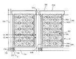
도 9는 본 발명의 제 1 실시예에 따른 액정 표시장치의 평면을 도시한 도면으로, 화소전극(164)과 공통전극(162)이 서로 엇갈리게 구성된다.9 is a diagram illustrating a plane of a liquid crystal display according to a first exemplary embodiment of the present invention, wherein the
도 9에 도시된 본 발명의 제 1 실시예에 따른 액정 표시장치의 구성을 더 자세히 설명하면, 가로방향으로는 게이트 배선(150)과 공통배선(160)이 서로 평행하게 배치되며, 세로방향으로는 데이터 배선(170)이 위치한다.Referring to the configuration of the liquid crystal display according to the first embodiment of the present invention shown in FIG. 9 in more detail, in the horizontal direction, the
상기 게이트 배선(150)과 데이터 배선(170)이 교차하는 부분에는 각각 게이트 전극(152)과 액티브층(154)과 소스 전극(156)이 형성되며, 상기 소스전극(156)과 대응하는 위치에는 드레인 전극(158)이 형성된다.The
한편, 가로방향으로 배열되는 상기 공통배선(160)에는 세로방향으로 다수 개로 분기되어 형성되는 공통전극(162)이 형성된다. 상기 공통전극(162)은 상기 데이터 배선(170)이 연장되는 방향으로 형성된다.On the other hand, the
그리고, 화소전극(164)은 상기 드레인전극(158)과 접촉하며 상기 공통전극(162)이 분기되어 형성되는 방향으로 상기 공통전극(162)과 서로 엇갈리게 형성된다.The
그리고, 상기 화소전극(164)및 상기 공통전극(162)의 상부에 형성된 감광성 유기막인 평탄화(overcoat layer)(미도시)막의 일부를 현상하여 홈(192)을 형성한다.A portion of the overcoat layer (not shown), which is a photosensitive organic layer formed on the
상기 홈(192)은 원형, 삼각형, 사각형, 육각형 등 다양한 형상으로 형성할 수 있다. 또한, 상기 홈(192)은 오버코팅(over coating)으로 사용할 수 있는 물질이면 가능하고 예를 들면, BCB나 아크릴레이트 계열을 사용할 수 있다. The
상기 홈(192)은 평면적으로 상기 공통전극(162)과 화소전극(164)에 걸쳐진 것과 같은 형상이고 각 전극에 엇갈려 구성한다.The
이후, 상기 평탄화막(미도시)의 상부에는 액정(194)이 위치하게 된다.Thereafter, the
화소영역(P)상에 서로 엇갈려 구성된 공통전극(162)과 화소전극(164)의 사이에 형성된 홈(192)은 상기 공통전극(162)과 화소전극(164)사이에 발생하는 전기장의 방향을 왜곡하여 왜곡전기장을 유발시키는 역할을 한다.The
이때, 상기 액정(194)은 유전이방성이 양인 포지티브(positive)액정을 사용하며, 액정의 초기배향은 전극(162,164)에 수평한 방향이 되도록 처리한다.In this case, the
그리고, 편광판의 편광축 방향은 전극(162,164)에 수평한 방향과 수직한 방향으로 정한다.The polarization axis direction of the polarizing plate is determined in a direction perpendicular to a direction horizontal to the
여기서, 상기 홈(192)은 화소전극(164)과 공통전극(162)을 번갈아 가며 각 전극이 연장된 방향으로 각 전극의 상부에 형성되게 되며, 예를 들어 각 화소전극을 동시에 가로지르는 제 1 가상선(C1)에 홈(192)이 형성되면, 다음에는 각 공통전극을 동시에 가로지르는 제 2 가상선(C2)에 홈(192)이 형성되며, 도메인은 상기 제 1, 2 가상선(C1, C2)의 사이에서 형성된다.Here, the
도 10은 도 9의 Ⅹ-Ⅹ을 절단한 단면도이다.10 is a cross-sectional view taken along the line VIII-VIII in FIG. 9.
도시한 바와 같이, 공통전극(162)과 화소전극(164)사이에는 제 1 절연막인 게이트 절연막(163)이 개재(介在)되어 있으며, 상기 공통전극(162)과 화소전극(164)이 구성된 기판(100)의 전면에 액정보다 작은 유전상수를 가지는 투명한 유기절연물질인 유전체막(유전율이 약 5 이하인 물질)을 증착하여 평탄화막(165)을 형성 한 후, 공통전극(162)과 화소전극(164)사이에 소정형상의 홈(192)을 형성한다.As illustrated, a substrate including a
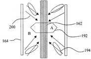
이하, 도 11의 평면도를 참조하여 상기 홈에서의 전기장의 왜곡현상을 설명한다.Hereinafter, the distortion phenomenon of the electric field in the groove will be described with reference to the plan view of FIG. 11.
도 11은 도 9의 K를 확대한 확대 평면도이다. 도시한 바와 같이, 상기 유전체의 유전상수가 액정의 유전상수보다 작은 값을 가지고 있기 때문에 홈(192)이 있는 부분(A)보다 홈이 없는 부분(B)에서의 전기력선의 밀도가 밀하게 되어 전기장의 왜곡현상이 발생한다.FIG. 11 is an enlarged plan view magnifying K of FIG. 9. As shown, since the dielectric constant of the dielectric has a smaller value than the dielectric constant of the liquid crystal, the density of the electric field lines in the non-groove portion B is denser than that of the groove portion A (192). Distortion occurs.
즉, 상기 홈(192)의 경계를 따라 전기장(200)이 꺽여들어가기 때문이다.That is, the
화소전극(164)과 공통전극(162)상부에 구성된 홈(192)을 중심으로 왜곡된 평행 전기장(200)을 유도한다.The distorted parallel
이 왜곡된 평행전기장(200)은 액정분자(194)에 좌우 방향으로의 회전력을 공급하게 되어 두가지 다른 도메인을 만들게 된다.The distorted parallel
여기서, 상기 홈(192)을 기준으로 상/하부에 인가되는 전기장은 서로 반대방향으로 흐트러지는 프린지필드(fringe field)가 형성된다. Here, a fringe field is formed in the electric field applied to the upper and lower parts of the
즉, 다시 설명하면, 상기 화소전극(164)을 사이에 두고, 상기 화소전극(164)의 양측에 형성된 공통전극(162)과 상기 화소전극(164)의 사이에 인가되는 전기장(200)은 상기 화소전극(164)의 상부에 형성된 홈(192)의 경계에서 왜곡되어 화소전극(164)으로 향하게 된다. In other words, the
따라서, 상기 홈(192)을 기준으로 상/하에 위치하는 액정(194)은 전기장의 인가에 따라 서로 다른 방향으로 배열하는 제 1, 2 도메인이 형성된다.Therefore, the
상기와 같이 홈(192)을 기준으로 서로 반대방향으로 액정(194)이 배열하는 이유는 액정의 자유도(degree of freedom)는 2가 되기 때문이다. The reason why the
즉, 도 12에 도시한 도면에서와 같이, 초기 액정의 분자 배열방향(즉, 배향방향)이 상기 화소전극(164) 및 공통전극(162)의 연장방향과 동일한 방향(d2 또는 d3)이라고 하면 액정의 초기 배열 방향(d1)이 화소전극(164) 및 공통전극(162)과 평행하게 위치하는 액정(194)은 전기장(200)이 인가되면, 액정의 장축은 전기장과 수평한 방향으로 재배열하게 된다.That is, as shown in FIG. 12, when the molecular arrangement direction (ie, alignment direction) of the initial liquid crystal is the same direction (d2 or d3) as the extension direction of the
따라서, 홈(192)을 기준으로 전기장의 왜곡된 방향이 각각 다르게 되므로, 서로 다른 도메인이 형성되게 된다.Therefore, since the distorted direction of the electric field is different with respect to the
전술한 바와 같이 본 발명의 제 1 실시예에 따라 제조된 횡전계 방식 액정표시장치는 평면내에서 액정이 두 방향으로 서로 나누어 회전하므로 시야각에 대한 색반전 효과를 각각의 도메인이 서로 보상한다.As described above, in the transverse electric field type liquid crystal display device manufactured according to the first embodiment of the present invention, since the liquid crystals are rotated by dividing each other in two directions in a plane, respective domains compensate each other for the color inversion effect on the viewing angle.
즉, 색반전을 줄일 수 있는 동시에, 그레이 인버전(grey inversion)이 없는 영역을 넓힐 수 있다.In other words, color inversion can be reduced, and an area without gray inversion can be widened.
이와 같은 효과는 네가티브 액정을 사용할 경우에도 동일하다.This effect is also the same when using a negative liquid crystal.
도 13에 도시한 바와 같이, 네가티브액정(195)은 상기 화소전극(도 11의 164)과 공통전극(도 11의 162)에 수직한 초기배향(d1)을 하며, 전기장이 인가되면 전기장의 방향과 액정(195)의 장축이 수직한 방향으로 배열된다.As shown in FIG. 13, the negative
따라서, 다수의 네가티브 액정은 초기배향 방향(d1)에서 제 1 방향(d2)과 이와는 대칭적인 제 2 방향(d3)으로 배향하여 서로 다른 도메인을 형성하게 된다.Therefore, the plurality of negative liquid crystals are aligned in the first direction d2 in the initial alignment direction d1 and in the second direction d3 which is symmetrical thereto to form different domains.
이하, 제 2 실시예는 상기 제 1 실시예의 구조를 변형한 것으로, 공통전극과 화소전극을 가로방향으로 형성한다.
The second embodiment is a modification of the structure of the first embodiment, and forms the common electrode and the pixel electrode in the horizontal direction.
-- 제 2 실시예 -- Second Embodiment
도 14는 본 발명의 제 2 실시예에 따른 횡전계방식 액정표시장치용 어레이기판의 일부를 도시한 평면도이다.14 is a plan view showing a part of an array substrate for a transverse electric field type liquid crystal display device according to a second embodiment of the present invention.
도시한 바와 같이, 게이트배선(250)과 데이터배선(270)을 서로 교차하여 구성하고, 상기 두 배선이 교차하는 지점에는 게이트전극(252)과 액티브층(254)과 소스전극(256)및 드레인전극(258)으로 구성된 박막트랜지스터(T)를 형성한다.As shown, the
또한, 상기 게이트배선(250)과 소정간격 이격하여 평행하게 일 방향으로 구성된 공통배선(260)을 형성한다.In addition, the
상기 공통배선(260)에서 화소영역(P)으로 분기된 공통전극(262)을 구성한다.The
이때, 상기 공통전극(262)은 상기 공통배선(260)에서 상기 화소영역(P)의 양측으로 각각 분기된 제 1 수직부(262a)와 제 2 수직부와(262b), 상기 제 1, 2 수직 부(262a,262b)를 연결하는 다수의 수평부(262c)로 구성한다.In this case, the
또한, 상기 드레인전극(258)과 접촉하는 화소전극(264)을 상기 화소영역(P)에 구성한다.
In addition, the
상기 화소전극(264)은 상기 공통배선(260)의 일부 상부에 구성된 제 1 수평부(264a)와, 상기 제 1 수평부(264a)의 양측에서 각각 수직하게 분기한 제 1 수직부(264b)와 제 2 수직부(264c)로 구성하며, 상기 두 수직부를 연결하는 다수의 제 2 수평부(264d)로 구성한다.The
이때, 상기 공통전극(262)의 수평부(262c)와 상기 화소전극(264)의 제 2 수평부(264d)는 서로 엇갈려 구성한다.In this case, the
이와 같은 구성에서, 다수의 홈(292)을 상기 화소전극(264)의 제 2 수평부(264d)와 공통전극(262)의 수평부(262c)의 연장된 방향으로 형성한다.In this configuration, the plurality of
상기 각 전극에 형성한 홈은 서로 나란히 구성하지 않고 각 전극마다 엇갈려 구성한다.The grooves formed in the electrodes are alternately configured for each electrode without forming them in parallel with each other.
이와 같은 구성은 화소전극을 동시에 가로지르는 제 1 가상선(C1)에 홈(292)이 형성되면, 다음에는 각 공통전극을 동시에 가로지르는 제 2 가상선(C2)에 홈(292)이 형성되며, 도메인은 상기 제 1, 2 가상선(C1, C2)의 사이에서 형성된다.
In this configuration, when the
이때, 전술한 바와 같은 어레이기판으로 구성을 가지는 액정표시장치에 사용되는 액정은 유전이방성이 양(+)인 포지티브(positive)액정(294)을 사용한다.In this case, the liquid crystal used in the liquid crystal display device having the array substrate as described above uses a positive
즉, 상기 액정은 공통전극(262)과 화소전극(264)의 각 수평성분(262c,264d)과 평행한 초기배향의 상태를 가진다.That is, the liquid crystal has an initial alignment state parallel to the
이와 같은 구성에서, 상기 화소전극(264)및 공통전극(262)과 수직한 초기배향을 가지는 네가티브 액정을 사용하여 원하는 2-도메인을 얻을 수 있다.
In such a configuration, a desired 2-domain can be obtained by using a negative liquid crystal having an initial alignment perpendicular to the
즉, 도 15에 도시한 바와 같이, 공통전극과 화소전극 사이에, 초기 액정의 분자 배열방향(즉, 배향방향)(d1)이 상기 화소전극 및 공통전극의 연장방향과 수직한 방향의 액정을 구성하면 앞서 설명한 바와 같이, 액정의 자유도는 2가 되기 때문에 초기배향된 액정을 중심으로 좌/우로 배열하게 된다. 이 때, 액정이 좌/우로 배열되게 하는 힘은 상기 홈(292)에 의해 흐트러지는 전기장 때문이며, 이 전기장에 의해서 2가지 서로 다른 도메인이 형성되게 되는 것이다.That is, as shown in FIG. 15, between the common electrode and the pixel electrode, a liquid crystal having a molecular arrangement direction (ie, an orientation direction) d1 of the initial liquid crystal is perpendicular to the extension direction of the pixel electrode and the common electrode. As described above, since the degree of freedom of the liquid crystal becomes 2, the left and right sides of the liquid crystal are initially arranged. At this time, the force causing the liquid crystal to be arranged left / right is due to the electric field disturbed by the
이하, 제 3 실시예는 상기 홈을 변형한 형태를 제시한다.
Hereinafter, the third embodiment presents a form in which the groove is modified.
-- 제 3 실시예 --Third Embodiment
도 16은 본 발명의 제 3 실시예에 따른 횡전계방식 액정표시장치용 어레이기판의 일부를 도시한 평면도이다.16 is a plan view showing a part of an array substrate for a transverse electric field type liquid crystal display device according to a third embodiment of the present invention.
도시한 바와 같이, 게이트 배선(350)과 공통배선(360)이 서로 평행하게 배치되며, 세로방향으로는 데이터 배선(370)이 위치한다.As illustrated, the
상기 게이트 배선(350)과 데이터 배선(370)이 교차하는 부분의 게이트 배선(350)과 데이터배선(370)에는 각각 게이트전극(352)과 액티브층(354)과 소스전극(356)이 형성되며, 상기 소스전극(356)과 대응하는 위치에는 드레인 전극(358)이 형성된다.A
한편, 가로방향으로 배열되는 상기 공통배선(360)에는 세로방향으로 다수 개로 분기되어 형성되는 공통전극(362)이 형성된다. 상기 공통전극(362)은 상기 데이터 배선(370)이 연장되는 방향으로 형성된다.
On the other hand, in the
그리고, 화소전극(364)은 상기 드레인전극(358)과 접촉하며, 상기 공통전극(362)과 서로 엇갈리게 형성된다.The
그리고, 상기 화소전극(364) 및 상기 공통전극(362)위에 형성된 감광성 평탄화막(미도시)의 일부를 현상(develope)하여 화소전극을 중심으로 "V"형상의 홈(392)을 형성한다. 상기 평탄화막(미도시)의 상부에는 상기 공통전극(362)과, 화소전극(364)에 평행한 초기배향상태의 액정(유전율 이방성이 양인 액정)이 위치한다. A portion of the photosensitive planarization film (not shown) formed on the
전술한 바와 같은 구성은, 상기 "V"형상의 홈(392)을 경계로 하여 "V"형태로 왜곡된 전기장(미도시)이 발생한다.In the above-described configuration, an electric field (not shown) distorted in the "V" shape is generated around the "V" shaped
따라서, 상기 전기장의 분포방향에 상기 액정(394)은 상기 화소전극(364)을 중심으로 서로 대칭적인 방향으로 배열된다. Accordingly, the
이하, 도 17을 참조하여, 상기 홈과 전기장분포에 대해 설명한다.Hereinafter, the grooves and the electric field distribution will be described with reference to FIG. 17.
도 17은 도 16의 L를 확대한 평면도로서, 도시한 바와 같이, 홈(392)의 내부인 A영역에서는 홈의 외부인 B영역 보다 전기장(300)의 전기력선이 밀하게 되어 전기장(300)이 상기 홈(392)의 경계에서 기울어지게 된다.FIG. 17 is an enlarged plan view of L of FIG. 16, and as shown in FIG. 16, in the region A inside the
따라서, 액정(394)의 회전방향은 상기 전기장의 기울어진 방향과 평행한 방향으로 회전하게 된다.Therefore, the rotation direction of the
따라서, 도 17에 도시한 바와 같이, 상기 액정은 상기 화소전극(364)을 중심으로 양측으로 대칭적인 방향으로 배향하게 되어 서로 다른 도메인을 형성하게 된다.
Thus, as shown in FIG. 17, the liquid crystal is aligned in both directions with respect to the
전술한 제 3 실시예의 구성에 네가티브 액정을 사용하여도 동일한 효과를 볼 수 있다.The same effect can be obtained even when negative liquid crystal is used in the configuration of the above-described third embodiment.
도 18에 도시한 바와 같이, 네가티브 액정(395)은 상기 화소전극과 공통전극에 수직한 초기 배향방향(d1)을 가지며, 전기장이 인가되면 도시한 바와 같이 제 1 방향(d2)또는 제 2 방향(d3)으로 배향되어 2-도메인을 형성할 수 있다.As shown in FIG. 18, the negative
전술한 바와 같은 구성은 각 전극을 중심으로 양측으로 대칭 되도록 전기장이 분포하는 형상이므로, 상기 전극을 중심으로 서로 보상관계에 있다.As described above, since the electric field is distributed so as to be symmetrical to both sides with respect to each electrode, the electrodes have a compensation relationship with each other.
따라서, 전극의 중앙에서 발생할 수 있는 전경선이 발생하지 않기 때문에 기존의 프린지 필드에 비해 프린지 필드가 강하여 외부 충격에 대한 복원력이 커지므로 응답특성이 빨라지고 외부 충격시 초기휘도의 복원이 더 짧은 시간내에 이루어진다.Therefore, since there is no foreground line that can occur at the center of the electrode, the fringe field is stronger than the existing fringe field, so the resilience against external impact is increased, resulting in faster response and restoration of initial luminance in a shorter time. .
또한, 상기 전경선이 발생하지 않으므로 기존에 2-도메인에 비해 개구율이 증가하고 휘도가 향상된다.In addition, since the foreground line does not occur, the aperture ratio is increased and the luminance is improved as compared with the conventional two-domain.
이하, 제 4 실시예는 상기 제 3 실시예의 구조를 변형한 것으로, 공통전극과 화소전극의 방향을 가로방향으로 서로 이격하여 구성한다.
Hereinafter, the fourth embodiment is a modification of the structure of the third embodiment, and the common electrodes and the pixel electrodes are spaced apart from each other in the horizontal direction.
-- 제 4 실시예 -- Fourth Embodiment
도 19는 본 발명의 제 4 실시예에 따른 횡전계 방식 액정표시장치용 어레이기판의 일부를 개략적으로 도시한 평면도이다. 19 is a plan view schematically illustrating a part of an array substrate for a transverse electric field type liquid crystal display device according to a fourth exemplary embodiment of the present invention.
도시한 바와 같이, 게이트배선(450)과 데이터배선(470)을 서로 교차하여 구성하고, 상기 두 배선이 교차하는 지점에는 게이트전극(452)과 액티브층(454)과 소스전극(456) 및 드레인전극(458)으로 구성된 박막트랜지스터(T)를 형성한다.As shown, the
상기 게이트배선(450)과 소정간격 이격하여 평행하게 일 방향으로 구성된 공통배선(460)을 형성한다.The
상기 공통배선(460)에서는 화소영역(P)으로 공통전극(462)을 분기하여 구성한다. 상기 공통전극(462)은 상기 화소영역(P)의 양측에서 수직하게 분기된 제 1 수직부(462a)와 제 2 수직부(462b)와, 상기 제 1, 2 수직부(462a,462b) 사이에 가로방향으로 구성한 수평부(462c)를 구성한다.In the
또한, 상기 드레인전극(458)과 접촉하는 화소전극(464)을 상기 화소영역(P)에 구성한다.In addition, a
상기 화소전극(464)은 상기 공통배선(460)의 일부 상부에 구성된 제 1 수평부(464a)와, 상기 제 1 수평부(464a)의 양측에서 각각 수직하게 분기한 제 1 수직부(464b)와 제 2 수직부(464c)로 구성하며, 상기 두 수직부를 연결하는 제 2 수평 부(464d)를 다수개 구성한다.The
이때, 상기 공통전극(462)의 수평부(462c)와 상기 화소전극(464)의 제 2 수평부(464d)는 소정간격 이격하여 서로 엇갈려 구성한다.In this case, the
이와 같은 구성에서, 상기 홈(492)은 상기 수평방향으로 구성된 화소전극(464)을 중심으로 "V"형상으로 구성한다.In this configuration, the
이때, 액정은 상기 화소전극과 공통전극의 방향과 평행한 초기배향을 가지는 포지티브 액정을 사용한다.In this case, the liquid crystal uses a positive liquid crystal having an initial alignment parallel to the directions of the pixel electrode and the common electrode.
이와 같은 구성은 앞서 설명한 바와 같은 2-도메인 효과를 나타낸다.Such a configuration exhibits a two-domain effect as described above.
이하, 도 20은 제 4 실시예에 구성된 네가티브 액정의 배향형태를 도시한 도면이다.20 is a view showing an alignment form of the negative liquid crystal configured in the fourth embodiment.
도시한 바와 같이, 네가티브 액정(495)은 상기 화소전극과 공통전극에 수직한 초기 배향방향(d1)을 가지며, 전기장이 인가되면 도시한 바와 같이 제 1 방향(d2)또는 제 2 방향(d3)으로 배향되어 2-도메인을 형성할 수 있다.As shown, the negative
전술한 바와 같은 구성으로 본 발명에 따른 횡전계방식 액정표시장치용 어레이기판을 제작할 수 있다.With the above-described configuration, an array substrate for a transverse electric field type liquid crystal display device according to the present invention can be manufactured.
상술한 바와 같이 본 발명에 따른 횡전계 방식 액정표시장치용 어레이기판을 제작하게 되면 다음과 같은 특징이 있다.As described above, the array substrate for the transverse electric field type liquid crystal display device according to the present invention has the following characteristics.
첫째, 종래의 횡전계방식 액정표시장치에서는 액정분자가 평면적으로 한 방향으로만 회전함으로 시야각에 따른 색반전의 특성이 존재하였으나, 본 발명에 따른 액정 표시장치에서는 적어도 2개의 서로 다른 반대 방향으로 회전하는 도메인이 형성됨에 따라 시야각에 따른 색반전의 특성을 개선할 수 있는 장점이 있다.First, in the conventional transverse electric field type liquid crystal display device, the liquid crystal molecules are rotated in one direction in a planar manner, so that there is a characteristic of color inversion according to the viewing angle. As the domain is formed, there is an advantage of improving the characteristics of color inversion according to the viewing angle.
둘째, 서로 다른 방향으로 회전하는 두 개의 도메인에 의해 시야각에 따른 계조반전의 특성을 개선할 수 있는 장점이 있다
Second, there is an advantage to improve the characteristics of gray scale inversion according to the viewing angle by the two domains that rotate in different directions
Claims (10)
Priority Applications (3)
| Application Number | Priority Date | Filing Date | Title |
|---|---|---|---|
| KR1020010045473A KR100833955B1 (en) | 2001-07-27 | 2001-07-27 | Array board for transverse electric field liquid crystal display |
| US10/201,785 US6885424B2 (en) | 2001-07-27 | 2002-07-25 | Array substrate for in-plane switching liquid crystal display device having multi-domain |
| US11/081,671 US7092060B2 (en) | 2001-07-27 | 2005-03-17 | Method for fabricating an array substrate for in-plane switching liquid crystal display device having multi-domain |
Applications Claiming Priority (1)
| Application Number | Priority Date | Filing Date | Title |
|---|---|---|---|
| KR1020010045473A KR100833955B1 (en) | 2001-07-27 | 2001-07-27 | Array board for transverse electric field liquid crystal display |
Publications (2)
| Publication Number | Publication Date |
|---|---|
| KR20030010422A KR20030010422A (en) | 2003-02-05 |
| KR100833955B1 true KR100833955B1 (en) | 2008-05-30 |
Family
ID=19712617
Family Applications (1)
| Application Number | Title | Priority Date | Filing Date |
|---|---|---|---|
| KR1020010045473A Expired - Fee Related KR100833955B1 (en) | 2001-07-27 | 2001-07-27 | Array board for transverse electric field liquid crystal display |
Country Status (2)
| Country | Link |
|---|---|
| US (2) | US6885424B2 (en) |
| KR (1) | KR100833955B1 (en) |
Families Citing this family (20)
| Publication number | Priority date | Publication date | Assignee | Title |
|---|---|---|---|---|
| US6876420B2 (en) * | 2002-06-25 | 2005-04-05 | Lg. Philips Lcd Co., Ltd. | In-plane switching mode liquid crystal display device |
| KR100887668B1 (en) * | 2002-12-30 | 2009-03-11 | 엘지디스플레이 주식회사 | Array board for transverse electric field type liquid crystal display device and manufacturing method thereof |
| TWI337678B (en) * | 2003-05-16 | 2011-02-21 | Chimei Innolux Corp | An active matrix liquid crystal display |
| KR100987887B1 (en) * | 2003-06-30 | 2010-10-13 | 엘지디스플레이 주식회사 | Transverse electric field mode liquid crystal display device |
| WO2006005230A1 (en) * | 2004-07-13 | 2006-01-19 | Quanta Display Inc. | Wide-viewing angle lcd device |
| CN1797139A (en) * | 2004-12-30 | 2006-07-05 | 鸿富锦精密工业(深圳)有限公司 | Switch inside plane type LCD device |
| JP4215019B2 (en) * | 2005-03-30 | 2009-01-28 | エプソンイメージングデバイス株式会社 | Liquid crystal device and electronic device |
| KR101134932B1 (en) * | 2005-06-14 | 2012-04-17 | 엘지디스플레이 주식회사 | Liquid crystal display device and method for fabricating thereof |
| KR101279114B1 (en) * | 2005-10-13 | 2013-06-26 | 엘지디스플레이 주식회사 | Liquid crystal display device |
| TWI545380B (en) * | 2006-05-16 | 2016-08-11 | 半導體能源研究所股份有限公司 | Liquid crystal display device and semiconductor device |
| WO2008001507A1 (en) * | 2006-06-26 | 2008-01-03 | Sharp Kabushiki Kaisha | Display |
| US8139185B2 (en) * | 2006-07-07 | 2012-03-20 | Sharp Kabushiki Kaisha | Display device |
| US8208102B2 (en) | 2006-07-21 | 2012-06-26 | Sharp Kabushiki Kaisha | Display device having reflective region and transmissive region |
| JP5093714B2 (en) * | 2006-07-25 | 2012-12-12 | Nltテクノロジー株式会社 | Liquid crystal display |
| EP2053452A3 (en) * | 2006-08-02 | 2012-03-14 | Sharp Kabushiki Kaisha | Display device |
| US8482709B2 (en) | 2010-04-22 | 2013-07-09 | Samsung Display Co., Ltd. | Liquid crystal display |
| KR101892710B1 (en) * | 2011-05-26 | 2018-08-29 | 삼성디스플레이 주식회사 | A liquid crystal display apparatus and the manufacturing method thereof |
| KR20130106219A (en) * | 2012-03-19 | 2013-09-27 | 삼성디스플레이 주식회사 | A display panel and a method for manufacturing the same |
| JP6411798B2 (en) * | 2014-07-10 | 2018-10-24 | Tianma Japan株式会社 | Liquid crystal display |
| CN112185315B (en) * | 2020-10-19 | 2022-04-26 | Tcl华星光电技术有限公司 | Liquid crystal display panel driving method, liquid crystal display panel and liquid crystal display device |
Citations (3)
| Publication number | Priority date | Publication date | Assignee | Title |
|---|---|---|---|---|
| KR19990056726A (en) * | 1997-12-29 | 1999-07-15 | 김영환 | LCD |
| KR20000020857A (en) * | 1998-09-24 | 2000-04-15 | 윤종용 | Liquid crystal display |
| KR20000023314A (en) * | 1998-09-22 | 2000-04-25 | 가나이 쓰토무 | Liquid crystal display device having photo-induced liquid crystal molecule alignment films |
Family Cites Families (20)
| Publication number | Priority date | Publication date | Assignee | Title |
|---|---|---|---|---|
| DE69333323T2 (en) * | 1992-09-18 | 2004-09-16 | Hitachi, Ltd. | A liquid crystal display device |
| JPH095764A (en) | 1995-06-20 | 1997-01-10 | Hitachi Ltd | LCD display substrate |
| JP3474975B2 (en) | 1995-09-06 | 2003-12-08 | 株式会社 日立ディスプレイズ | Liquid crystal display device and method of manufacturing the same |
| JPH09105908A (en) | 1995-10-09 | 1997-04-22 | Hitachi Ltd | Active matrix type liquid crystal display |
| JP3632934B2 (en) | 1995-10-04 | 2005-03-30 | 株式会社 日立ディスプレイズ | Active matrix liquid crystal display device |
| US5745207A (en) * | 1995-11-30 | 1998-04-28 | Matsushita Electric Industrial Co., Ltd. | Active matrix liquid crystal display having electric fields parallel to substrates |
| JP3396130B2 (en) * | 1996-06-03 | 2003-04-14 | シャープ株式会社 | Liquid crystal display |
| JP2776376B2 (en) * | 1996-06-21 | 1998-07-16 | 日本電気株式会社 | Active matrix liquid crystal display panel |
| US6005648A (en) * | 1996-06-25 | 1999-12-21 | Semiconductor Energy Laboratory Co., Ltd. | Display device |
| JPH10142633A (en) * | 1996-11-15 | 1998-05-29 | Mitsubishi Electric Corp | Thin film transistor integrated device, method of manufacturing the same, and liquid crystal display device |
| US6226061B1 (en) * | 1997-03-25 | 2001-05-01 | Sharp Kabushiki Kaisha | Liquid crystal display device having phase different plates |
| KR100257369B1 (en) * | 1997-05-19 | 2000-05-15 | 구본준 | In plane switching mode liquid crystal display device |
| KR100477130B1 (en) * | 1997-09-25 | 2005-08-29 | 삼성전자주식회사 | Thin Film Transistor Board and Manufacturing Method of Flat Drive Liquid Crystal Display |
| JP3228202B2 (en) * | 1997-11-18 | 2001-11-12 | 日本電気株式会社 | Lateral electric field type active matrix liquid crystal display device and method of manufacturing the same |
| US6287899B1 (en) * | 1998-12-31 | 2001-09-11 | Samsung Electronics Co., Ltd. | Thin film transistor array panels for a liquid crystal display and a method for manufacturing the same |
| TW498178B (en) * | 2000-05-02 | 2002-08-11 | Hannstar Display Corp | Manufacturing method and structure for in-plane switching mode liquid crystal display unit |
| JP2001330849A (en) * | 2000-05-18 | 2001-11-30 | Nec Corp | Liquid crystal display device |
| JP2002023171A (en) * | 2000-07-11 | 2002-01-23 | Nec Corp | Liquid crystal display device and manufacturing method therefor |
| JP2002040456A (en) * | 2000-07-28 | 2002-02-06 | Nec Corp | Liquid crystal display device |
| KR100748442B1 (en) * | 2001-02-26 | 2007-08-10 | 엘지.필립스 엘시디 주식회사 | Array board for horizontal electric field drive type liquid crystal display device and manufacturing method thereof |
-
2001
- 2001-07-27 KR KR1020010045473A patent/KR100833955B1/en not_active Expired - Fee Related
-
2002
- 2002-07-25 US US10/201,785 patent/US6885424B2/en not_active Expired - Lifetime
-
2005
- 2005-03-17 US US11/081,671 patent/US7092060B2/en not_active Expired - Lifetime
Patent Citations (3)
| Publication number | Priority date | Publication date | Assignee | Title |
|---|---|---|---|---|
| KR19990056726A (en) * | 1997-12-29 | 1999-07-15 | 김영환 | LCD |
| KR20000023314A (en) * | 1998-09-22 | 2000-04-25 | 가나이 쓰토무 | Liquid crystal display device having photo-induced liquid crystal molecule alignment films |
| KR20000020857A (en) * | 1998-09-24 | 2000-04-15 | 윤종용 | Liquid crystal display |
Also Published As
| Publication number | Publication date |
|---|---|
| US20050157239A1 (en) | 2005-07-21 |
| US6885424B2 (en) | 2005-04-26 |
| US7092060B2 (en) | 2006-08-15 |
| US20030020861A1 (en) | 2003-01-30 |
| KR20030010422A (en) | 2003-02-05 |
Similar Documents
| Publication | Publication Date | Title |
|---|---|---|
| KR100833955B1 (en) | Array board for transverse electric field liquid crystal display | |
| JP6240432B2 (en) | Liquid crystal display | |
| JP3966614B2 (en) | Wide viewing angle LCD | |
| US6256081B1 (en) | LCD of high aperture ratio and high transmittance preventing color shift having transparent pixel and counter electrodes producing oblique electric fields | |
| KR100494702B1 (en) | Fringe field switching liquid crystal display | |
| KR100921137B1 (en) | Liquid crystal display | |
| KR20130034700A (en) | Liquid crystal display | |
| CN101925853A (en) | Liquid crystal display device having a plurality of pixel electrodes | |
| KR101147090B1 (en) | Liquid Crystal Display Device | |
| US7113240B2 (en) | Liquid crystal display device having insulating patterns with width larger than gap in between | |
| WO2011040080A1 (en) | Liquid crystal display device | |
| JP2004151525A (en) | Liquid crystal display | |
| JP2001235748A (en) | Multi-domain liquid crystal display | |
| KR100924747B1 (en) | Wide viewing angle liquid crystal display device | |
| KR100345957B1 (en) | In Plane Switching mode Liquid crystal display device | |
| KR100903650B1 (en) | Liquid crystal display | |
| KR20160064322A (en) | Liquid crystal display | |
| US7663721B2 (en) | Multi-domain vertical alignment liquid crystal display panel | |
| KR100566811B1 (en) | Array panel for in-plane switching mode liquid crystal display | |
| KR100773875B1 (en) | Transverse electric field mode liquid crystal display | |
| US20020033914A1 (en) | Liquid crystal display device and method of fabricating the same | |
| KR100579545B1 (en) | Array panel for in-plane switching mode liquid crystal display | |
| KR100835969B1 (en) | Transverse electric field liquid crystal display device | |
| KR100658074B1 (en) | Cross-field switching mode liquid crystal display device with improved transmittance and afterimage | |
| KR20040105470A (en) | In plane switching mode liquid crystal display device and fabrication method thereof |
Legal Events
| Date | Code | Title | Description |
|---|---|---|---|
| PA0109 | Patent application |
St.27 status event code: A-0-1-A10-A12-nap-PA0109 |
|
| PG1501 | Laying open of application |
St.27 status event code: A-1-1-Q10-Q12-nap-PG1501 |
|
| A201 | Request for examination | ||
| P11-X000 | Amendment of application requested |
St.27 status event code: A-2-2-P10-P11-nap-X000 |
|
| P13-X000 | Application amended |
St.27 status event code: A-2-2-P10-P13-nap-X000 |
|
| PA0201 | Request for examination |
St.27 status event code: A-1-2-D10-D11-exm-PA0201 |
|
| R17-X000 | Change to representative recorded |
St.27 status event code: A-3-3-R10-R17-oth-X000 |
|
| E902 | Notification of reason for refusal | ||
| PE0902 | Notice of grounds for rejection |
St.27 status event code: A-1-2-D10-D21-exm-PE0902 |
|
| P11-X000 | Amendment of application requested |
St.27 status event code: A-2-2-P10-P11-nap-X000 |
|
| P13-X000 | Application amended |
St.27 status event code: A-2-2-P10-P13-nap-X000 |
|
| E902 | Notification of reason for refusal | ||
| PE0902 | Notice of grounds for rejection |
St.27 status event code: A-1-2-D10-D21-exm-PE0902 |
|
| E13-X000 | Pre-grant limitation requested |
St.27 status event code: A-2-3-E10-E13-lim-X000 |
|
| P11-X000 | Amendment of application requested |
St.27 status event code: A-2-2-P10-P11-nap-X000 |
|
| P13-X000 | Application amended |
St.27 status event code: A-2-2-P10-P13-nap-X000 |
|
| PN2301 | Change of applicant |
St.27 status event code: A-3-3-R10-R13-asn-PN2301 St.27 status event code: A-3-3-R10-R11-asn-PN2301 |
|
| E701 | Decision to grant or registration of patent right | ||
| PE0701 | Decision of registration |
St.27 status event code: A-1-2-D10-D22-exm-PE0701 |
|
| GRNT | Written decision to grant | ||
| PR0701 | Registration of establishment |
St.27 status event code: A-2-4-F10-F11-exm-PR0701 |
|
| PR1002 | Payment of registration fee |
St.27 status event code: A-2-2-U10-U11-oth-PR1002 Fee payment year number: 1 |
|
| PG1601 | Publication of registration |
St.27 status event code: A-4-4-Q10-Q13-nap-PG1601 |
|
| R18-X000 | Changes to party contact information recorded |
St.27 status event code: A-5-5-R10-R18-oth-X000 |
|
| PR1001 | Payment of annual fee |
St.27 status event code: A-4-4-U10-U11-oth-PR1001 Fee payment year number: 4 |
|
| R18-X000 | Changes to party contact information recorded |
St.27 status event code: A-5-5-R10-R18-oth-X000 |
|
| R18-X000 | Changes to party contact information recorded |
St.27 status event code: A-5-5-R10-R18-oth-X000 |
|
| FPAY | Annual fee payment |
Payment date: 20120330 Year of fee payment: 5 |
|
| PR1001 | Payment of annual fee |
St.27 status event code: A-4-4-U10-U11-oth-PR1001 Fee payment year number: 5 |
|
| FPAY | Annual fee payment |
Payment date: 20130329 Year of fee payment: 6 |
|
| PR1001 | Payment of annual fee |
St.27 status event code: A-4-4-U10-U11-oth-PR1001 Fee payment year number: 6 |
|
| PR1001 | Payment of annual fee |
St.27 status event code: A-4-4-U10-U11-oth-PR1001 Fee payment year number: 7 |
|
| FPAY | Annual fee payment |
Payment date: 20150429 Year of fee payment: 8 |
|
| PR1001 | Payment of annual fee |
St.27 status event code: A-4-4-U10-U11-oth-PR1001 Fee payment year number: 8 |
|
| FPAY | Annual fee payment |
Payment date: 20160428 Year of fee payment: 9 |
|
| PR1001 | Payment of annual fee |
St.27 status event code: A-4-4-U10-U11-oth-PR1001 Fee payment year number: 9 |
|
| FPAY | Annual fee payment |
Payment date: 20170413 Year of fee payment: 10 |
|
| PR1001 | Payment of annual fee |
St.27 status event code: A-4-4-U10-U11-oth-PR1001 Fee payment year number: 10 |
|
| LAPS | Lapse due to unpaid annual fee | ||
| PC1903 | Unpaid annual fee |
St.27 status event code: A-4-4-U10-U13-oth-PC1903 Not in force date: 20180527 Payment event data comment text: Termination Category : DEFAULT_OF_REGISTRATION_FEE |
|
| PC1903 | Unpaid annual fee |
St.27 status event code: N-4-6-H10-H13-oth-PC1903 Ip right cessation event data comment text: Termination Category : DEFAULT_OF_REGISTRATION_FEE Not in force date: 20180527 |