KR100821289B1 - Flexible Optical Circuit Board and Manufacturing Method Thereof - Google Patents
Flexible Optical Circuit Board and Manufacturing Method Thereof Download PDFInfo
- Publication number
- KR100821289B1 KR100821289B1 KR1020070009416A KR20070009416A KR100821289B1 KR 100821289 B1 KR100821289 B1 KR 100821289B1 KR 1020070009416 A KR1020070009416 A KR 1020070009416A KR 20070009416 A KR20070009416 A KR 20070009416A KR 100821289 B1 KR100821289 B1 KR 100821289B1
- Authority
- KR
- South Korea
- Prior art keywords
- flexible
- copper foil
- optical
- hole
- light
- Prior art date
- Legal status (The legal status is an assumption and is not a legal conclusion. Google has not performed a legal analysis and makes no representation as to the accuracy of the status listed.)
- Active
Links
- 230000003287 optical effect Effects 0.000 title claims abstract description 167
- 238000004519 manufacturing process Methods 0.000 title claims abstract description 17
- RYGMFSIKBFXOCR-UHFFFAOYSA-N Copper Chemical compound [Cu] RYGMFSIKBFXOCR-UHFFFAOYSA-N 0.000 claims abstract description 85
- 239000011889 copper foil Substances 0.000 claims abstract description 48
- 229910052802 copper Inorganic materials 0.000 claims abstract description 41
- 239000010949 copper Substances 0.000 claims abstract description 41
- 239000010410 layer Substances 0.000 claims description 50
- 239000002184 metal Substances 0.000 claims description 21
- 229910052751 metal Inorganic materials 0.000 claims description 21
- 238000000034 method Methods 0.000 claims description 18
- 238000005530 etching Methods 0.000 claims description 9
- 230000001681 protective effect Effects 0.000 claims description 9
- 239000012792 core layer Substances 0.000 claims description 7
- 239000004642 Polyimide Substances 0.000 claims description 5
- 229920001721 polyimide Polymers 0.000 claims description 5
- 229910052782 aluminium Inorganic materials 0.000 claims description 4
- 229910052737 gold Inorganic materials 0.000 claims description 4
- 238000012545 processing Methods 0.000 claims description 4
- 229910052709 silver Inorganic materials 0.000 claims description 4
- 238000005553 drilling Methods 0.000 claims description 3
- 229910052697 platinum Inorganic materials 0.000 claims description 2
- 230000000149 penetrating effect Effects 0.000 claims 1
- 108091008695 photoreceptors Proteins 0.000 claims 1
- 238000010168 coupling process Methods 0.000 description 12
- 230000008878 coupling Effects 0.000 description 11
- 238000005859 coupling reaction Methods 0.000 description 11
- 230000005540 biological transmission Effects 0.000 description 8
- 239000000758 substrate Substances 0.000 description 8
- 238000005253 cladding Methods 0.000 description 5
- 239000011810 insulating material Substances 0.000 description 5
- 229920000106 Liquid crystal polymer Polymers 0.000 description 4
- 239000004977 Liquid-crystal polymers (LCPs) Substances 0.000 description 4
- 229910000679 solder Inorganic materials 0.000 description 4
- 238000012986 modification Methods 0.000 description 3
- 230000004048 modification Effects 0.000 description 3
- 229920000642 polymer Polymers 0.000 description 3
- 238000011161 development Methods 0.000 description 2
- 238000010586 diagram Methods 0.000 description 2
- 238000003754 machining Methods 0.000 description 2
- 238000003491 array Methods 0.000 description 1
- 238000004891 communication Methods 0.000 description 1
- 230000000694 effects Effects 0.000 description 1
- 238000007772 electroless plating Methods 0.000 description 1
- 238000005516 engineering process Methods 0.000 description 1
- 230000010354 integration Effects 0.000 description 1
- 238000010295 mobile communication Methods 0.000 description 1
- 239000013307 optical fiber Substances 0.000 description 1
- 229920002120 photoresistant polymer Polymers 0.000 description 1
- 239000004033 plastic Substances 0.000 description 1
- 238000007747 plating Methods 0.000 description 1
- 229920001690 polydopamine Polymers 0.000 description 1
- 230000000644 propagated effect Effects 0.000 description 1
- 238000007514 turning Methods 0.000 description 1
- XLYOFNOQVPJJNP-UHFFFAOYSA-N water Substances O XLYOFNOQVPJJNP-UHFFFAOYSA-N 0.000 description 1
Images


Classifications
-
- H—ELECTRICITY
- H05—ELECTRIC TECHNIQUES NOT OTHERWISE PROVIDED FOR
- H05K—PRINTED CIRCUITS; CASINGS OR CONSTRUCTIONAL DETAILS OF ELECTRIC APPARATUS; MANUFACTURE OF ASSEMBLAGES OF ELECTRICAL COMPONENTS
- H05K1/00—Printed circuits
- H05K1/02—Details
- H05K1/0274—Optical details, e.g. printed circuits comprising integral optical means
-
- G—PHYSICS
- G02—OPTICS
- G02B—OPTICAL ELEMENTS, SYSTEMS OR APPARATUS
- G02B6/00—Light guides; Structural details of arrangements comprising light guides and other optical elements, e.g. couplings
- G02B6/24—Coupling light guides
- G02B6/42—Coupling light guides with opto-electronic elements
- G02B6/4201—Packages, e.g. shape, construction, internal or external details
- G02B6/4204—Packages, e.g. shape, construction, internal or external details the coupling comprising intermediate optical elements, e.g. lenses, holograms
- G02B6/4214—Packages, e.g. shape, construction, internal or external details the coupling comprising intermediate optical elements, e.g. lenses, holograms the intermediate optical element having redirecting reflective means, e.g. mirrors, prisms for deflecting the radiation from horizontal to down- or upward direction toward a device
-
- H—ELECTRICITY
- H01—ELECTRIC ELEMENTS
- H01S—DEVICES USING THE PROCESS OF LIGHT AMPLIFICATION BY STIMULATED EMISSION OF RADIATION [LASER] TO AMPLIFY OR GENERATE LIGHT; DEVICES USING STIMULATED EMISSION OF ELECTROMAGNETIC RADIATION IN WAVE RANGES OTHER THAN OPTICAL
- H01S5/00—Semiconductor lasers
- H01S5/10—Construction or shape of the optical resonator, e.g. extended or external cavity, coupled cavities, bent-guide, varying width, thickness or composition of the active region
- H01S5/18—Surface-emitting [SE] lasers, e.g. having both horizontal and vertical cavities
-
- H—ELECTRICITY
- H05—ELECTRIC TECHNIQUES NOT OTHERWISE PROVIDED FOR
- H05K—PRINTED CIRCUITS; CASINGS OR CONSTRUCTIONAL DETAILS OF ELECTRIC APPARATUS; MANUFACTURE OF ASSEMBLAGES OF ELECTRICAL COMPONENTS
- H05K3/00—Apparatus or processes for manufacturing printed circuits
- H05K3/40—Forming printed elements for providing electric connections to or between printed circuits
- H05K3/42—Plated through-holes or plated via connections
- H05K3/429—Plated through-holes specially for multilayer circuits, e.g. having connections to inner circuit layers
Landscapes
- Physics & Mathematics (AREA)
- Engineering & Computer Science (AREA)
- General Physics & Mathematics (AREA)
- Optics & Photonics (AREA)
- Microelectronics & Electronic Packaging (AREA)
- Condensed Matter Physics & Semiconductors (AREA)
- Electromagnetism (AREA)
- Manufacturing & Machinery (AREA)
- Optical Integrated Circuits (AREA)
Abstract
본 발명은 연성 광 회로기판 및 그 제조 방법에 관한 것으로서, 연성 동박적층판의 상부 동박층에 접속되는 구동칩, 상기 구동칩에 의해 구동되는 광원부, 상기 광원부로부터 광신호를 전달하기 위해서 상기 광원부에 정렬되어 위치하는 관통홀 어레이가 형성된 광 송신부; 연성 동박적층판의 상부 동박층에 접속되는 구동칩, 상기 구동칩에 의해 구동되는 광 검출부, 상기 광 검출부로부터 광신호를 수신하기 위해서 상기 광 검출부에 정렬되어 위치하는 관통홀 어레이가 형성된 광 수신부; 및 상기 광 송신부와 상기 광 수신부와 정렬된 관통홀 어레이에 대응하여 광 접속을 위해 반사 거울면을 형성하여 상기 연성 동박적층판의 하부 동박층에 배치되는 연성 광 도파로를 포함하여, 광신호의 속도향상과 전달손실을 최소화할 수 있도록 하며 모듈의 소형화할 수 있는 이점이 있다.The present invention relates to a flexible optical circuit board and a method of manufacturing the same, comprising: a driving chip connected to an upper copper foil layer of a flexible copper clad laminate, a light source unit driven by the driving chip, and an optical signal from the light source unit to be aligned; An optical transmitter having a through hole array positioned thereon; A light receiving unit having a driving chip connected to the upper copper foil layer of the flexible copper foil laminated plate, a light detecting unit driven by the driving chip, and a through-hole array arranged in alignment with the light detecting unit to receive an optical signal from the light detecting unit; And a flexible optical waveguide disposed on the lower copper foil layer of the flexible copper clad laminate to form a reflective mirror surface for optical connection corresponding to the through-hole array aligned with the optical transmitter and the optical receiver. It can minimize the over-transmission loss and has the advantage of miniaturization of the module.
Description
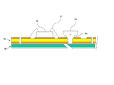
도1은 본 발명의 일실시예에 따른 연성 광 회로기판의 개략 단면도이다.1 is a schematic cross-sectional view of a flexible optical circuit board according to an embodiment of the present invention.
도2는 본 발명의 일실시예에 따른 연성 광 회로기판의 평면도이다.2 is a plan view of a flexible optical circuit board according to an embodiment of the present invention.
도3a 내지 도3l은 본 발명의 일실시예에 따른 연성 광 회로기판의 제조공정도이다.3A to 3L are manufacturing process diagrams of a flexible optical circuit board according to an embodiment of the present invention.
도4는 본 발명의 일실시예에 따른 연성 광 회로기판의 또 다른 계략 단면도이다.4 is another schematic cross-sectional view of a flexible optical circuit board according to an embodiment of the present invention.
<도면의 주요 부분에 대한 부호의 설명> <Explanation of symbols for the main parts of the drawings>
10 : 연성 동박적층판 11, 13 : 동박층10: flexible copper foil laminated
12 : 절연재 14 : 광원부12: insulating material 14: light source
15, 25 : 구동칩 17, 27 : 본딩 와이어15, 25: driving
20, 40 : 관통홀 24 : 광 검출부20, 40: through hole 24: light detector
28 : 금속 반사면 50 : 연성 광도파로28: metal reflective surface 50: flexible optical waveguide
51 : 코어층 52, 53 : 클래드층 51:
55 : 반사 거울면 65 : 솔더범프55
70 : 상하정렬 홀 80 : 하우징70: vertical alignment hole 80: housing
90 : 보호필름 100 : 광송신부 90: protective film 100: light transmitting unit
200 : 광수신부 200: light receiving unit
본 발명은 연성 광 회로기판 및 그 제조 방법에 관한 것으로서, 더욱 상세하게는 광신호를 방출하고 수신하는 광송신부와 광수신부를 구성하는 연성 동박적층판에서 광신호의 전송통로로서 관통홀을 형성하고 연성의 광 도파로를 수직 광 결합시킴으로써 다양한 연성 동박적층판을 이용하여 저렴하게 제작이 가능하고 소형의 제품 구현이 가능한 연성 광 회로기판 및 그 제조 방법에 관한 것이다. The present invention relates to a flexible optical circuit board and a method of manufacturing the same, and more particularly, a through hole is formed as a transmission path of an optical signal in a flexible copper foil laminate comprising an optical transmitter and an optical receiver that emits and receives an optical signal. The present invention relates to a flexible optical circuit board and a method of manufacturing the same, which can be manufactured at low cost by using various flexible copper clad laminates and can realize a small product by vertically coupling an optical waveguide of the optical waveguide.
일반적으로 저속의 전자 시스템에서 회로 기판과 회로기판, 칩과 칩 또는 시스템간의 연결은 전기적인 금속 배선을 통하여 이루어지나, 대용량 병렬 컴퓨터로 구성되는 차세대 정보통신 시스템이나 1Tb/s급 이상의 ATM 스위칭 시스템 등에서와 같이 정보가 대용량화되고, 전송 속도가 향상됨에 따라 이러한 금속 배선을 이용할 경우 스큐(skew), EMI(electromagnetic interference) 등과 같은 전기적인 문제가 발생되어 시스템의 동작 효율이 저하되고 시스템 집적화가 어려워진다.In general, in low-speed electronic systems, the connection between circuit boards and circuit boards, chips and chips or systems is made through electrical metal wiring, but in next-generation information and communication systems consisting of large parallel computers or ATM switching systems of 1 Tb / s or more As the information is increased in volume and the transmission speed is improved, electrical problems such as skew, electromagnetic interference (EMI), etc. are generated when the metal wiring is used, and thus the operation efficiency of the system is reduced and system integration becomes difficult.
근래에 들어 이동통신 분야의 발전으로 3G, 4G와 같은 미래의 휴대폰과 PDA에서 디지털 TV를 시청하거나 녹화가 가능할 것으로 예상되며 이로 인한 데이터 요구량이 증가할 것으로 예상된다.In recent years, with the development of mobile communication, it is expected that digital TV can be watched or recorded in future mobile phones and PDAs such as 3G and 4G, and the data demand is expected to increase.
또한, 향후 더 높은 전송 요구량에 따라 메인보드와 디스플레이 사이를 연결 하는 기존의 폴리이미드를 이용하는 전기전송의 연성회로기판(flexible PCB)은 전송의 한계에 도달하게 된다.In addition, in accordance with higher transmission requirements in the future, the flexible PCB of the electrical transmission using the existing polyimide that connects between the motherboard and the display will reach the limit of transmission.
한편, 최근에 광 송신/수신 모듈을 이용하여 광 연결을 이루는 기술이 개발되었는데, 광 송신/수신 모듈 내부의 광 결합 방식으로는 45°의 경사각으로 위치된 반사경을 구비하는 리본 광섬유 다채널 광 콘넥터에 광 수신 소자를 직접 결합시키는 방식, 45°의 경사각으로 위치된 반사경을 구비하는 폴리머(polymer) 광도파로에 광 송수신 소자를 폴리머 광도파로에 수직으로 결합시키고 폴리머 광도파로를 다채널 광 콘넥터에 연결시키는 방식, 플라스틱 팩키지에 고정된 광 송수신 소자를 다채널 광 콘넥터에 수직으로 결합시키는 방식 등이 이용된다.On the other hand, recently, a technology for making an optical connection by using an optical transmission / reception module has been developed. In the optical coupling method inside the optical transmission / reception module, a ribbon optical fiber multichannel optical connector having a reflector positioned at an inclination angle of 45 ° is provided. Direct coupling of the optical receiving element to the polymer optical waveguide having a reflector positioned at an inclination angle of 45 °, and vertically coupling the optical transmitting and receiving element to the polymer optical waveguide and connecting the polymer optical waveguide to the multichannel optical connector. And a method of vertically coupling the optical transmission / reception element fixed to the plastic package to the multi-channel optical connector.
상기 광원에서 광을 수직 연결하여 광 도파로로 결합하는 기술은 "광모듈" 또는 "광 접속 모듈"로 알려져 있다.The technique of vertically connecting light in the light source and coupling the light waveguide is known as an "optical module" or an "optical connection module".
종래의 연성 동박적층판(Flexible Copper Clad Laminate)을 이용한 광결합 소자에 있어서, 광신호의 전송을 위해서는 광학적으로 투명한 절연층을 이용해야 한다.In a conventional optical coupling device using a flexible copper clad laminate, an optically transparent insulating layer must be used to transmit an optical signal.
현재 상업적으로 판매되는 연성 동박적층판의 절연층은 광학적으로 불투명한 폴리이미드(polyimide)나 LCP(liquid crystal polymer)를 이용하기 때문에 광회로 기판에는 사용이 불가능한 문제점이 있다.Currently, the insulating layer of a commercially available flexible copper clad laminate uses an optically opaque polyimide or liquid crystal polymer (LCP), which makes it impossible to use an optical circuit board.
또한, 종래의 연성 광회로 기판은 광도파로와 VCSEL 또는 포토다이오드 사이의 광정렬을 위해서는 단면의 연성 동박적층판만을 사용해야 하기 때문에 저속 데이터 신호나 전원 공급을 위한 신호 라인을 단면에 모두 형성해야 한다. 따라서, 연성 동박적층판이 넓어지는 문제가 발생한다.In addition, in the conventional flexible optical circuit board, only the flexible copper-clad laminate having a cross section is used for the optical alignment between the optical waveguide and the VCSEL or the photodiode, so that a low-speed data signal or a signal line for power supply must be formed on the cross section. Therefore, a problem arises in that the flexible copper clad laminate is widened.
본 발명은 상술한 바와 같은 종래의 문제점을 해결하기 위하여 연성 동박적층판을 이용하여 광송신부와 광수신부를 포함하는 연성 광 회로기판에 관통홀 구조를 통하여, 광도파로와 수직 연결함으로써 광접속을 하여 절연층의 특성에 영향을 받지 않게 되어 연성 동박적층판에 제작되는 연성 광 회로 기판 및 그 제조 방법을 제공하기 위한 것이다.In order to solve the above-mentioned problems, the present invention uses a flexible copper-clad laminate to insulate an optical connection by vertically connecting with an optical waveguide through a through-hole structure to a flexible optical circuit board including an optical transmitter and an optical receiver. It is for providing the flexible optical circuit board which is not influenced by the characteristic of a layer, and is manufactured to a flexible copper clad laminated board, and its manufacturing method.
또한, 연성 회로기판상에 광송신부와 광수신부를 형성하고, 상기 광송신부와 광수신부에 형성된 관통홀에 정렬하여 양면의 연성 동박적층판을 사용할 수 있으므로 기판의 폭을 반으로 줄여 소형의 제품 제작이 가능한 연성 광 회로기판 및 그 제조 방법을 제공하기 위한 것이다. In addition, since a light transmitting part and a light receiving part are formed on the flexible circuit board, and the double-sided flexible copper clad laminates can be used by aligning with the through holes formed in the light transmitting part and the light receiving part, it is possible to reduce the width of the board in half and to manufacture a small product. It is to provide a flexible optical circuit board and a manufacturing method thereof.
상기와 같은 종래의 문제점을 해결하고 상기 목적을 달성하기 위한 본 발명에 따른 연성 광 회로기판은, 연성 동박적층판의 상부 동박층에 접속되는 구동칩, 상기 구동칩에 의해 구동되는 광원부, 상기 광원부로부터 광신호를 전달하기 위해서 상기 광원부에 정렬되어 위치하는 관통홀 어레이가 형성된 광 송신부; 연성 동박적층판의 상부 동박층에 접속되는 구동칩, 상기 구동칩에 의해 구동되는 광 검출부, 상기 광 검출부로부터 광신호를 수신하기 위해서 상기 광 검출부에 정렬되어 위치하는 관통홀 어레이가 형성된 광 수신부; 및 상기 광 송신부에 정렬된 관통홀 어레이와, 상기 광 수신부와 정렬된 관통홀 어레이에 각각 대응하여 광 접속을 위 해 반사 거울면을 형성하여 상기 연성 동박적층판의 하부 동박층에 배치되는 연성 광 도파로를 포함한다.The flexible optical circuit board according to the present invention for solving the above conventional problems and to achieve the above object is a drive chip connected to the upper copper foil layer of the flexible copper clad laminate, a light source unit driven by the drive chip, from the light source unit An optical transmitter having an array of through holes arranged in alignment with the light source to transmit an optical signal; A light receiving unit having a driving chip connected to the upper copper foil layer of the flexible copper foil laminated plate, a light detecting unit driven by the driving chip, and a through-hole array arranged in alignment with the light detecting unit to receive an optical signal from the light detecting unit; And a reflective optical waveguide disposed on the lower copper foil layer of the flexible copper clad laminate by forming a reflective mirror surface for optical connection corresponding to the through hole array aligned with the optical transmitter and the through hole array aligned with the light receiver. It includes.
또한, 본 발명에 따른 상기 연성 광 회로기판은 상기 관통홀 어레이의 관통홀 내부 표면에 금속막이 코팅된 것을 특징으로 하는 것이다.In addition, the flexible optical circuit board according to the present invention is characterized in that the metal film is coated on the inner surface of the through hole of the through hole array.
또한, 본 발명에 따른 상기 연성 광 회로기판에 있어서, 상기 관통홀의 내부 표면에 코팅된 금속막은 Au, Ag, Cu, Al 또는 Pt에서 선택되는 것을 특징으로 하는 것이다. In the flexible optical circuit board according to the present invention, the metal film coated on the inner surface of the through hole may be selected from Au, Ag, Cu, Al, or Pt.
또한, 본 발명에 따른 상기 연성 광 회로기판에 있어서, 상기 광 송신부는 광원부로서 표면방출레이저(VCSEL) 어레이를 포함하는 것을 특징으로 하는 것이다.In the flexible optical circuit board according to the present invention, the light transmitting unit includes a surface emitting laser (VCSEL) array as a light source unit.
또한, 본 발명에 따른 상기 연성 광 회로기판에 있어서, 상기 광수신부는 광 검출부로서 포토 다이오드 어레이를 포함하는 것을 특징으로 하는 것이다.In the flexible optical circuit board according to the present invention, the light receiving unit includes a photodiode array as a light detector.
또한, 본 발명에 따른 상기 연성 광 회로기판에 있어서, 상기 연성 광도파로의 표면은 보호필름이 더 부가되어 있는 것을 특징으로 하는 것이다.Further, in the flexible optical circuit board according to the present invention, the surface of the flexible optical waveguide is characterized in that a protective film is further added.
또한, 본 발명에 따른 상기 연성 광 회로기판에 있어서, 상기 광 송신부와 광 수신부, 구동칩, 본딩와이어, 광원부 또는 광 검출부에는 보호용 하우징을 구비하는 것을 특징으로 하는 것이다.In the flexible optical circuit board according to the present invention, a protective housing is provided in the light transmitting unit, the light receiving unit, the driving chip, the bonding wire, the light source unit or the light detecting unit.
또한, 본 발명에 따른 상기 연성 광 회로기판에 있어서, 상기 연성 광도파로의 반사 거울면은 45° 반사 거울면 또는 곡면 반사 거울면인 것을 특징으로 하는 것이다. In the flexible optical circuit board according to the present invention, the reflective mirror surface of the flexible optical waveguide is a 45 ° reflective mirror surface or a curved reflective mirror surface.
또한, 본 발명에 따른 상기 연성 광 회로기판에 있어서, 상기 연성 동박적층 판에는 절연층으로서 폴리이미드 또는 LCP가 포함되어 있는 것을 특징으로 하는 것이다.In the flexible optical circuit board according to the present invention, the flexible copper clad laminate may include polyimide or LCP as an insulating layer.
한편, 본 발명에 따른 연성 광 회로기판의 제조방법은, 연성 동박적층판에 상하 정렬 홀을 가공하여 형성하는 단계; 상기 연성 동박적층판의 상부에서 회로전극 패턴 형성을 위해 동박층을 에칭하는 단계; 상기 연성 동박적층판의 관통홀이 형성될 부분에 드릴 가공하여 절연층을 관통하는 단계; 상기 연성 동박적층판의 하부 동박층에 하부 클래드층, 코어층, 상부 클래드층을 적층하여 연성 광도파로를 형성하는 단계; 상기 연성 동박적층판의 상부 동박층에 마스크층을 도포하여 노광, 현상한 후 관통홀이 형성될 부분을 에칭하는 단계; 상기 연성 광도파로에서 상기 관통홀 형성부분에 대응하는 위치에서 반사 거울면을 형성하는 단계; 및 상기 연성 동박적층판 상부 동박층의 회로전극 패턴 위에 광원부, 광검출부, 구동칩을 상기 관통홀 부분과 정렬하고 실장하는 단계를 포함한다.On the other hand, the method of manufacturing a flexible optical circuit board according to the present invention, the step of forming by forming a vertical alignment hole in the flexible copper foil laminated plate; Etching the copper foil layer to form a circuit electrode pattern on the flexible copper foil laminate; Drilling a portion of the flexible copper clad laminate to be formed with a through hole to penetrate the insulating layer; Stacking a lower clad layer, a core layer, and an upper clad layer on the lower copper foil layer of the flexible copper clad laminate to form a flexible optical waveguide; Applying a mask layer to the upper copper foil layer of the flexible copper foil laminate to expose and develop the etching, and etching the portion where the through hole is to be formed; Forming a reflective mirror surface at a position corresponding to the through hole forming portion in the flexible optical waveguide; And arranging and mounting a light source unit, a photodetector unit, and a driving chip on the circuit electrode pattern of the upper copper foil layer of the flexible copper clad laminate plate with the through hole portion.
또한, 본 발명에 따른 상기 연성 광 회로기판의 제조방법에 있어서, 상기 연성 동박적층판 상부 동박층의 회로전극 패턴 위에 실장된 광원부, 구동칩을 포함하는 광송신부와 광검출부, 구동칩을 포함하는 광수신부를 보호하는 하우징을 부가하는 단계를 더 포함하는 것을 특징으로 하는 것이다.In addition, in the method of manufacturing the flexible optical circuit board according to the present invention, a light source unit mounted on a circuit electrode pattern of the upper copper foil layer of the flexible copper clad laminate, a light transmitting unit including a driving chip, a light detecting unit including a driving chip, and a light water including a driving chip Adding a housing for protecting the bride is characterized in that it further comprises.
또한, 본 발명에 따른 상기 연성 광 회로기판의 제조방법에 있어서, 상기 연성 동박적층판에 형성된 관통홀의 내부 표면에 금속 반사면을 형성하는 단계를 더 포함하는 것을 특징으로 하는 것이다.In addition, the method of manufacturing the flexible optical circuit board according to the present invention, characterized in that it further comprises the step of forming a metal reflective surface on the inner surface of the through-hole formed in the flexible copper-clad laminate.
또한, 본 발명에 따른 상기 연성 광 회로기판의 제조방법에 있어서, 상기 연 성 광도파로의 표면에 보호필름을 부착하는 단계를 추가로 포함하는 것을 특징으로 하는 것이다.In addition, the method of manufacturing the flexible optical circuit board according to the present invention, characterized in that it further comprises the step of attaching a protective film on the surface of the flexible optical waveguide.
이하, 본 발명에 대하여 첨부된 도면을 참조하여 도면에 도시된 실시예에 대하여 더욱 상세히 설명한다. Hereinafter, exemplary embodiments of the present invention will be described in detail with reference to the accompanying drawings.
도1은 본 발명의 일실시예에 따른 연성 광 회로기판의 개략도이고, 도2는 본 발명의 일실시예에 따른 연성 광 회로기판의 부분 평면도이다.1 is a schematic diagram of a flexible optical circuit board according to an embodiment of the present invention, and FIG. 2 is a partial plan view of a flexible optical circuit board according to an embodiment of the present invention.
도1을 참조하면, 본 발명의 일실시예에 연성 광 회로기판은 광송신부(100)와 광수신부(200), 상기 광송신부(100)와 광수신부(200) 사이에서 광신호를 전달하는 광도파로(50)로 이루어진다.Referring to FIG. 1, a flexible optical circuit board according to an embodiment of the present invention includes an
도1에서 상기 광송신부(100)와 상기 광수신부(200)는 연성 동박적층판(10) 상에 형성되어 있다. In FIG. 1, the
상기 연성 동박적층판(10)은 가운데에 절연재인 폴리이미드(Polyimide) 또는 LCP가 충진되고 상하부에 동박층(11, 13)이 적층된 구조를 하고 있다. The flexible
상기 광송신부(100)는 연성 동박적층판(10)의 상부 동박층(11)에 접속되는 구동칩(15), 상기 구동칩(15)에 의해 구동되는 광원부(14), 상기 광원부(14)로부터 광신호를 전달하기 위해서 상기 광원부(14)에 정렬되어 위치하는 관통홀 어레이(20)가 형성된다.The
한편, 상기 광수신부(200)는 상기 연성 동박적층판(10)의 상부 동박층(11)에 접속되는 구동칩(25), 상기 구동칩(25)에 의해 구동되는 광 검출부(24), 상기 광 검출부(24)로부터 광신호를 수신하기 위해서 상기 광 검출부(24)에 정렬되어 위치 하는 관통홀 어레이(40)가 형성된다.The
또한, 본 발명에 따른 연성 광 회로기판은 상기 광 송신부(100) 및 상기 광 수신부(200)와 정렬된 관통홀 어레이(20, 40)에 각각 대응하여 광 접속을 위해 반사 거울면(55)을 형성하고 상기 연성 동박적층판(10)의 하부 동박층(13)에 배치되는 연성 광 도파로(50)를 포함한다. In addition, the flexible optical circuit board according to the present invention corresponds to the through-
상기 광 도파로(50)는 가운데에 코어층(51)과 상기 코어층(51)과 인접하여 상하 양쪽 방향으로 클래드층(52, 53)이 위치하여 있다. In the
상기 반사 거울면은 45° 반사 거울면 또는 곡면의 반사 거울면이 사용될 수 있으나, 바람직하게는 45° 반사 거울면이 사용된다. The reflective mirror surface may be a 45 ° reflective mirror surface or a curved reflective mirror surface, but preferably a 45 ° reflective mirror surface is used.
상기 광 송신부(100)에는 광원부(14)로서 VCSEL(Vertical Cavity Surface Emitting Laser) 어레이가 실장되고 상기 VCSEL 어레이로부터 연성 광도파로(50)로 광신호를 전달하는 관통홀 어레이(20)에는 금속 반사면이 형성될 수 있다. The
여기서, 상기 연성 동박적층판(10)에 형성된 상기 관통홀 어레이(20)의 내벽에 도금되는 금속은 Au, Ag, Cu, Al, Pt에서 선택할 수 있다.Here, the metal to be plated on the inner wall of the through-
또한, 상기 광 수신부(200)에는 광검출부(24)로서 포토다이오드(Photo Diode) 어레이가 사용된다. In addition, a photo diode array is used as the
상기 연성 동박적층판(10)에는 광송신부(100) 또는 광수신부(200)에서 광원부(14) 또는 광 검출부(24)를 구동하기 위한 구동칩(15, 25)에 전기 신호 전달을 위한 회로패턴을 포함한다.The flexible copper-clad
또한, 연성 동박적층판(10)과 구동칩(15)의 연결 및 구동칩(15)과 광원 부(14)인 VCSEL 또는 광검출부(24)인 포토다이오드 어레이가 위치하는 전극패드 사이의 연결은 본딩 와이어(bonding wire, 17)를 이용한다. In addition, the connection between the flexible copper-clad
상기 VCSEL 어레이 및 포토다이오드 어레이는 연성 동박적층판(10)에 솔더범프(solder bump, 65)를 이용하여 플립칩 본딩 방식으로 실장된다. The VCSEL array and the photodiode array are mounted on the flexible copper clad
또한, 도2에 도시된 바와 같이 상기 VCSEL 어레이는 상기 연성 동박적층판(10)의 금속(11)에 패턴 형성된 전극패드(60) 위에 솔더 범프(65)로 배치되고, 상기 VCSEL 어레이가 위치된 전극패드(60)는 본딩 와이어(17)에 의하여 구동칩(15)과 연결되어 있다. 상기 연결 방식은 광 수신부(200)의 경우에도 동일하게 적용됨은 물론이다.In addition, as shown in FIG. 2, the VCSEL array is disposed as a
한편, 상기 광 송신부(100)와 광 수신부(200)를 형성하는 기판(10)에는 상기 기판(10)상에 패턴 형성된 전자회로패턴, 구동칩(15, 25), 본딩와이어(17), 광원부(14) 또는 광 검출부(24)를 보호하는 하우징(80)을 더 구비할 수 있다.The
또한, 도1, 도2에서 도시된 바와 같이, 상기 연성 동박적층판(10)에는 상부의 기판과 상기 기판에 부착되는 하부의 연성 광도파로에 광 신호를 전달하는 통로가 되는 관통홀을 레이저 가공하기 위한 레이저 가공 정렬 마크(70)를 포함한다. In addition, as shown in Fig. 1, 2, the flexible copper-clad
또한, 상기 연성 광도파로(50)의 표면에는 보호필름(90)이 더 부가되어 연성 광도파로(50)를 보호하도록 한다.In addition, a
도1, 2를 참조하여 본 발명의 일실시예에 따른 연성 광 회로기판의 동작을 상세하게 설명한다.1 and 2 will be described in detail the operation of the flexible optical circuit board according to an embodiment of the present invention.
먼저 메인보드로부터 전달된 전기적 신호는 VCSEL을 구동하는 구동칩(15)에 전달되고, VCSEL을 구동하는 상기 구동칩(15)은 광원부(14)인 VCSEL 어레이를 독립적으로 각각 구동하여 고속 변조된 광신호를 방출한다. First, the electrical signal transmitted from the main board is transmitted to the
방출된 광신호는 연성 동박적층판(10)의 관통홀 어레이(20)를 통과하여 방출되고, 방출된 광신호는 연성 광도파로(50)의 45°반사 거울면(55)에서 반사되어 연성 광도파로(50)의 코어(51)에 입사된다. The emitted optical signal is emitted through the through-
상기 연성 광도파로(50)의 코어(51)를 통해 전파된 광신호는 광수신부(200)의 연성 광도파로(50) 단부의 45° 반사 거울면(55)에 의해서 반사되어 광수신부(200)의 의 관통홀 어레이(40)를 통과하여 광검출부(24)로 입사되고, 상기 광검출부(24)에 의해서 전기적 신호로 변환된 후 메인보드에 전달된다.The optical signal propagated through the
또한, 관통홀의 내부 표면을 금속으로 도금하면 VCSEL 발광부에서 방출된 광신호가 도금된 금속에 의해서 전반사하여 VCSEL과 광도파로 사이의 결합손실을 더 줄일 수 있다.In addition, when the inner surface of the through hole is plated with metal, the optical signal emitted from the VCSEL light emitting part is totally reflected by the plated metal, thereby further reducing coupling loss between the VCSEL and the optical waveguide.
동일하게, 광수신부에서도 이와 같이 관통홀의 내부 표면을 금속 도금함으로써 광도파로와 포토다이오드 사이의 결합 손실을 더 줄일 수 있다. Similarly, in the light receiving unit, the coupling loss between the optical waveguide and the photodiode can be further reduced by metal plating the inner surface of the through hole.
한편, 도면에서 도시된 화살표는 상술한 바와 같이 광신호가 광송신부(100)에서 방출되어 광수신부(200)로 전달되는 경로를 나타낸다.On the other hand, the arrow shown in the drawing indicates a path in which the optical signal is emitted from the
도3a 내지 도3l은 본 발명의 일실시예에 따른 연성 광 회로기판의 제작 공정을 나타내는 단면도이다.3A to 3L are cross-sectional views illustrating a fabrication process of a flexible optical circuit board according to an embodiment of the present invention.
먼저, 연성 광 회로기판을 제작하기 위하여 도 3a와 같이 가운데에 절연재(12)와 상기 절연재(12) 상하부에 동박층(11, 13)이 적층 형성되어 있는 연성 동 박적층판에 드릴 가공하여 상하 정렬홀(70)을 가공한다. First, in order to fabricate a flexible optical circuit board, as shown in FIG. 3A, a drill is drilled into a flexible copper laminated board in which copper foil layers 11 and 13 are laminated on upper and lower portions of the insulating
상기 상하 정렬홀(70)은 전술한 바와 같이 상부의 기판(10)과 상기 기판에 부착되는 하부의 연성 광도파로(50)의 반사거울면(55)에 정확하게 결합하여 광 신호를 전달하는 통로가 되는 관통홀(20, 40)을 레이저 가공하기 위한 것이다.As described above, the
도3b는 연성 광 회로기판의 관통홀(20, 40)을 형성하기 위한 첫 단계로서 연성 동박적층판(10)의 상부 동박층(11)을 에칭하는 과정을 나타낸다.3B illustrates a process of etching the upper
다음으로, 도3c는 상기 연성 광회로기판의 연성 동박적층판(10)에서 상부 동박층(11)이 에칭된 부분에 레이저 가공을 하여 상기 연성 동박적층판(10)의 절연재 부분(12)을 뚫는 과정을 나타낸다.Next, FIG. 3C illustrates a process of drilling the insulating
도3d는 상기 도3b, 도3c에서 동박층(11)을 가공 처리한 회로패턴과 관통홀(20)이 가공 형성된 연성 광회로기판의 연성 동박적층판(10)을 상하를 뒤집어서 아래의 하부 동박층(13)을 위로 하고 상기 하부 동박층(13)에 하부 클래드층(52)을 적층하는 모습을 나타낸다.FIG. 3D shows the circuit pattern of the
도3e에서는 클래딩(52)위에 코어층(51)을 패터닝하고, 도3f는 상기 코어층(51)에 다시 상부 클래드층(53)을 적층하여 연성 광도파로(50)를 형성하는 과정을 나타낸다. In FIG. 3E, the
도3g는 상기 연성 동박적층판(10)의 상부 동박층(11)에 마스크층(56)을 도포하여 노광, 현상한 후 관통홀(20)이 형성될 부분을 에칭하는 단계를 나타낸다.3G illustrates a step of applying a
상기 마스크층(56)으로는 패턴이 형성된 포토레지스트 또는 드라이 필름이 적용된다.A patterned photoresist or dry film is applied to the
도3h는 상기 연성 동박적층판(10)의 하부 동박층(13)을 에칭하여 완전한 관통홀(20)을 형성하는 과정을 나타낸다. 3H illustrates a process of etching the lower
도3i, 도3j는 상기 연성 광도파로(50)에 비스듬하게 레이저 가공을 하여 45° 반사 거울면(55)을 형성하는 과정을 나타낸다.3I and 3J illustrate a process of forming the 45 °
상기 반사 거울면(55)은 상기 연성 광도파로(50)에 정렬 형성된 관통홀(20) 어레이와 결합하여 광 접속 통로의 역할을 한다.The
도3k는 상기 연성 광회로기판의 연성 동박적층판(10) 위에 구동칩(15)과 광원부(14)를 솔더 범프(65)를 사용하여 실장하고 본딩 와이어(17)로 연결하여 배치한 모습을 나타낸다.FIG. 3K shows the
도3l은 상기 광 송신부(100)와 광 수신부(200)를 형성하는 연성 동박적층판(10) 위에 패턴 형성된 전자회로패턴, 구동칩(15), 본딩와이어(17), 광원부(14) 또는 광 검출부(24)를 보호하는 하우징(80)을 설치하고, 상기 기판(10)과 결합된 상기 연성 광도파로(50)의 클래딩을 보호하기 위하여 연성 광도파로(50)의 표면에 보호필름(90)이 더 부가된 것을 나타낸다.3L illustrates an electronic circuit pattern, a
도면에 도시된 화살표는 광송신부(100)에서 관통홀(20)을 통해서 나오는 광신호가 연성 광도파로(50)의 반사 거울면(55)에 반사되어 광 도파로(50)를 통과하는 모습을 나타낸다.Arrows shown in the drawing indicate that the optical signal from the
한편, 도4는 본 발명의 일실시예에 따른 연성 광 회로기판의 단면도로서, 관통홀 내벽에 금속 반사면을 형성한 것을 나타낸다. On the other hand, Figure 4 is a cross-sectional view of a flexible optical circuit board according to an embodiment of the present invention, showing a metal reflective surface formed on the inner wall of the through hole.
상기 연성 동박적층판(10)과 연성 광도파로(50)의 광결합에 있어서, 광결합 의 효율을 높이기 위한 것으로, 상기 광신호를 전달하는 관통홀(20) 어레이에는 금속 반사면(28)이 형성된다. In the optical coupling of the flexible copper clad
상기 가공된 관통홀(20) 각각의 내부 표면에는 금속 도금하여 광신호의 전반사를 이루도록 금속 반사면을 형성한다. The inner surface of each of the processed through
여기서, 상기 금속 반사면은 Au, Ag, Cu, Al 또는 Pt에서 선택하여 무전해 도금으로 형성될 수 있다.Here, the metal reflective surface may be formed by electroless plating by selecting from Au, Ag, Cu, Al, or Pt.
도면에 도시된 화살표는 광송신부(100)에서 관통홀(20)을 통해서 나오는 광신호가 연성 광도파로(50)의 반사 거울면(55)을 거쳐서 전송되는 경로를 나타낸다.Arrows shown in the drawing indicate a path through which the optical signal from the
도4에 도시된 부분은 광송신부(100)를 나타내고 있으나, 광수신부(200)의 경우에도 동일하게 적용할 수 있다.Although the part shown in FIG. 4 shows the
이상에서 살펴본 바와 같이 본 발명에 따른 연성 광 회로기판 및 그 제조 방법에 따르면 연성 동박적층판을 이용하여 광송신부와 광수신부를 포함하는 연성 광 회로기판에 관통홀 구조를 통하여, 광도파로와 수직 연결에 의한 광접속을 함으로써 절연층의 특성에 영향을 받지 않게 되어 연성 동박적층판 상에 연성 광 회로 기판을 제조할 수 있게 되는 효과가 있다.As described above, according to the flexible optical circuit board and the manufacturing method thereof according to the present invention, the flexible optical circuit board using the flexible copper-clad laminate, through the through-hole structure in the flexible optical circuit board including the optical transmitter and the optical receiver, through the optical waveguide and the vertical connection By the optical connection by this, there is an effect that the flexible optical circuit board can be manufactured on the flexible copper foil laminated plate since the characteristics of the insulating layer are not affected.
또한, 광송신부와 광수신부에 형성된 관통홀에 정렬하여 양면의 연성 동박적층판을 사용할 수 있으므로 기판의 폭을 반으로 줄여 소형의 제품 제작이 가능하게 된다.In addition, since the flexible copper-clad laminate of both sides can be used in alignment with the through-holes formed in the light transmitting unit and the light receiving unit, the width of the substrate can be reduced in half, thereby making it possible to manufacture small products.
이상에서 본 발명은 기재된 구체적인 실시예에 대해서만 상세히 설명되었지 만 본 발명의 기술사상 범위 내에서 다양한 변형 및 수정이 가능함은 당업자에게 있어서 명백한 것이며, 이러한 변형 및 수정이 첨부된 특허청구범위에 속함은 당연한 것이다.Although the present invention has been described in detail only with respect to the specific embodiments described, it will be apparent to those skilled in the art that various modifications and variations are possible within the technical scope of the present invention, and such modifications and modifications belong to the appended claims. will be.
Claims (13)
Priority Applications (1)
| Application Number | Priority Date | Filing Date | Title |
|---|---|---|---|
| KR1020070009416A KR100821289B1 (en) | 2007-01-30 | 2007-01-30 | Flexible Optical Circuit Board and Manufacturing Method Thereof |
Applications Claiming Priority (1)
| Application Number | Priority Date | Filing Date | Title |
|---|---|---|---|
| KR1020070009416A KR100821289B1 (en) | 2007-01-30 | 2007-01-30 | Flexible Optical Circuit Board and Manufacturing Method Thereof |
Publications (1)
| Publication Number | Publication Date |
|---|---|
| KR100821289B1 true KR100821289B1 (en) | 2008-04-11 |
Family
ID=39534531
Family Applications (1)
| Application Number | Title | Priority Date | Filing Date |
|---|---|---|---|
| KR1020070009416A Active KR100821289B1 (en) | 2007-01-30 | 2007-01-30 | Flexible Optical Circuit Board and Manufacturing Method Thereof |
Country Status (1)
| Country | Link |
|---|---|
| KR (1) | KR100821289B1 (en) |
Cited By (6)
| Publication number | Priority date | Publication date | Assignee | Title |
|---|---|---|---|---|
| KR100985764B1 (en) * | 2008-11-03 | 2010-10-06 | (주)인터플렉스 | Method for manufacturing flexible printed circuit board with optical waveguide |
| KR101059642B1 (en) * | 2008-11-28 | 2011-08-25 | 삼성전기주식회사 | Printed circuit board having optical waveguide and manufacturing method thereof |
| KR101545939B1 (en) | 2008-10-27 | 2015-08-21 | 삼성디스플레이 주식회사 | Light source module, method of manufacturing same, and backlight assembly having same |
| CN107918111A (en) * | 2017-12-18 | 2018-04-17 | 成都聚利中宇科技有限公司 | High frequency millimeter swash frequency-scan radar receiving and transmitting front end module |
| WO2021072987A1 (en) | 2019-10-16 | 2021-04-22 | Compass Technology Company Limited | Integrated electro-optical flexible circuit board |
| US20230012678A1 (en) * | 2020-02-12 | 2023-01-19 | Nitto Denko Corporation | Opto-electric hybrid board and opto-electric composite transmission module |
Citations (4)
| Publication number | Priority date | Publication date | Assignee | Title |
|---|---|---|---|---|
| JPH07202423A (en) * | 1993-12-29 | 1995-08-04 | Nippon Chemicon Corp | Guide trench and formation of multi-connection through hole |
| JP2000235127A (en) * | 1999-02-15 | 2000-08-29 | Nippon Telegr & Teleph Corp <Ntt> | Optoelectronic integrated circuit and method of manufacturing the same |
| KR20050062141A (en) * | 2003-12-19 | 2005-06-23 | 삼성전기주식회사 | Method for processing optical waveguide entrance of printed circuit board |
| JP2006284781A (en) * | 2005-03-31 | 2006-10-19 | Furukawa Electric Co Ltd:The | Circuit board |
-
2007
- 2007-01-30 KR KR1020070009416A patent/KR100821289B1/en active Active
Patent Citations (4)
| Publication number | Priority date | Publication date | Assignee | Title |
|---|---|---|---|---|
| JPH07202423A (en) * | 1993-12-29 | 1995-08-04 | Nippon Chemicon Corp | Guide trench and formation of multi-connection through hole |
| JP2000235127A (en) * | 1999-02-15 | 2000-08-29 | Nippon Telegr & Teleph Corp <Ntt> | Optoelectronic integrated circuit and method of manufacturing the same |
| KR20050062141A (en) * | 2003-12-19 | 2005-06-23 | 삼성전기주식회사 | Method for processing optical waveguide entrance of printed circuit board |
| JP2006284781A (en) * | 2005-03-31 | 2006-10-19 | Furukawa Electric Co Ltd:The | Circuit board |
Cited By (12)
| Publication number | Priority date | Publication date | Assignee | Title |
|---|---|---|---|---|
| KR101545939B1 (en) | 2008-10-27 | 2015-08-21 | 삼성디스플레이 주식회사 | Light source module, method of manufacturing same, and backlight assembly having same |
| KR100985764B1 (en) * | 2008-11-03 | 2010-10-06 | (주)인터플렉스 | Method for manufacturing flexible printed circuit board with optical waveguide |
| KR101059642B1 (en) * | 2008-11-28 | 2011-08-25 | 삼성전기주식회사 | Printed circuit board having optical waveguide and manufacturing method thereof |
| CN107918111A (en) * | 2017-12-18 | 2018-04-17 | 成都聚利中宇科技有限公司 | High frequency millimeter swash frequency-scan radar receiving and transmitting front end module |
| WO2021072987A1 (en) | 2019-10-16 | 2021-04-22 | Compass Technology Company Limited | Integrated electro-optical flexible circuit board |
| US11076491B2 (en) | 2019-10-16 | 2021-07-27 | Compass Technology Company Limited | Integrated electro-optical flexible circuit board |
| CN114730054A (en) * | 2019-10-16 | 2022-07-08 | 金柏科技有限公司 | Integrated electro-optical flexible circuit board |
| JP2022552301A (en) * | 2019-10-16 | 2022-12-15 | コンパス テクノロジー カンパニー リミテッド | Integrated electro-optic flexible circuit board |
| US11553598B2 (en) | 2019-10-16 | 2023-01-10 | Compass Technology Company Limited | Integrated electro-optical flexible circuit board |
| EP4045955A4 (en) * | 2019-10-16 | 2023-12-27 | Compass Technology Company Limited | INTEGRATED ELECTRO-OPTIC FLEXIBLE CIRCUIT BOARD |
| CN114730054B (en) * | 2019-10-16 | 2025-02-28 | 厦门金柏半导体有限公司 | Integrated electro-optical flexible circuit board |
| US20230012678A1 (en) * | 2020-02-12 | 2023-01-19 | Nitto Denko Corporation | Opto-electric hybrid board and opto-electric composite transmission module |
Similar Documents
| Publication | Publication Date | Title |
|---|---|---|
| KR100460703B1 (en) | Electro-optical circuit board having unified optical transmission/receiving module and optical waveguide | |
| US8363993B2 (en) | Combined optical and electrical interconnection module and method for producing same | |
| JP3833132B2 (en) | Manufacturing method of optical waveguide device | |
| US7406229B2 (en) | Optical module | |
| EP1975659A1 (en) | Photoelectric conversion module for direct optical interconnection and method of manufacturing the same | |
| KR100871251B1 (en) | Optical module | |
| JP4923402B2 (en) | Optical module and electrical wiring board | |
| WO2013046415A1 (en) | Optical module | |
| US20050025435A1 (en) | Optical module and manufacturing method of the same, optical-communication apparatus, and electronic apparatus | |
| KR100821289B1 (en) | Flexible Optical Circuit Board and Manufacturing Method Thereof | |
| JP5692581B2 (en) | Photoelectric conversion module and method for manufacturing photoelectric conversion module | |
| US7499614B2 (en) | Passive alignment of VCSELs to waveguides in opto-electronic cards and printed circuit boards | |
| JP2004163722A (en) | Component embedded board | |
| KR20040059627A (en) | A printed circuit board being packaged optical devices of multi-channel block type | |
| JP5277874B2 (en) | Opto-electric hybrid board and electronic equipment | |
| KR100452136B1 (en) | Architecture of optical interconnection using optical connection rods in waveguide-embedded multi-layer circuit board | |
| KR100734906B1 (en) | Optical interconnect using flexible optical printed circuit board | |
| JP2008158090A (en) | Optical wiring board | |
| KR20080049881A (en) | Flexible Optical Connection Module for Flat Panel Display and Manufacturing Method Thereof | |
| KR100901445B1 (en) | Flexible optical connection module combined with connector and manufacturing method thereof | |
| KR100874116B1 (en) | Photoelectric conversion module | |
| KR100901446B1 (en) | Package structure of optical connection module and its manufacturing method | |
| KR100864962B1 (en) | Flexible Optical Connection Module for Flat Panel Display and Manufacturing Method Thereof | |
| JP2022191844A (en) | semiconductor package | |
| JP5477576B2 (en) | Optical substrate manufacturing method |
Legal Events
| Date | Code | Title | Description |
|---|---|---|---|
| A201 | Request for examination | ||
| PA0109 | Patent application |
Patent event code: PA01091R01D Comment text: Patent Application Patent event date: 20070130 |
|
| PA0201 | Request for examination | ||
| E902 | Notification of reason for refusal | ||
| PE0902 | Notice of grounds for rejection |
Comment text: Notification of reason for refusal Patent event date: 20071108 Patent event code: PE09021S01D |
|
| E701 | Decision to grant or registration of patent right | ||
| PE0701 | Decision of registration |
Patent event code: PE07011S01D Comment text: Decision to Grant Registration Patent event date: 20080227 |
|
| GRNT | Written decision to grant | ||
| PR0701 | Registration of establishment |
Comment text: Registration of Establishment Patent event date: 20080403 Patent event code: PR07011E01D |
|
| PR1002 | Payment of registration fee |
Payment date: 20080403 End annual number: 3 Start annual number: 1 |
|
| PG1601 | Publication of registration | ||
| PR1001 | Payment of annual fee |
Payment date: 20110405 Start annual number: 4 End annual number: 4 |
|
| PR1001 | Payment of annual fee |
Payment date: 20120404 Start annual number: 5 End annual number: 5 |
|
| FPAY | Annual fee payment |
Payment date: 20130306 Year of fee payment: 6 |
|
| PR1001 | Payment of annual fee |
Payment date: 20130306 Start annual number: 6 End annual number: 6 |
|
| FPAY | Annual fee payment |
Payment date: 20140416 Year of fee payment: 7 |
|
| PR1001 | Payment of annual fee |
Payment date: 20140416 Start annual number: 7 End annual number: 7 |
|
| FPAY | Annual fee payment |
Payment date: 20160308 Year of fee payment: 9 |
|
| PR1001 | Payment of annual fee |
Payment date: 20160308 Start annual number: 9 End annual number: 9 |
|
| FPAY | Annual fee payment |
Payment date: 20170331 Year of fee payment: 10 |
|
| PR1001 | Payment of annual fee |
Payment date: 20170331 Start annual number: 10 End annual number: 10 |
|
| FPAY | Annual fee payment |
Payment date: 20180403 Year of fee payment: 11 |
|
| PR1001 | Payment of annual fee |
Payment date: 20180403 Start annual number: 11 End annual number: 11 |
|
| FPAY | Annual fee payment |
Payment date: 20190403 Year of fee payment: 12 |
|
| PR1001 | Payment of annual fee |
Payment date: 20190403 Start annual number: 12 End annual number: 12 |
|
| PR1001 | Payment of annual fee |
Payment date: 20220404 Start annual number: 15 End annual number: 15 |
|
| PR1001 | Payment of annual fee |
Payment date: 20230403 Start annual number: 16 End annual number: 16 |
|
| PR1001 | Payment of annual fee |
Payment date: 20240226 Start annual number: 17 End annual number: 17 |