KR100809750B1 - Manufacturing Method of Thin Film Transistor - Google Patents
Manufacturing Method of Thin Film Transistor Download PDFInfo
- Publication number
- KR100809750B1 KR100809750B1 KR1020010017167A KR20010017167A KR100809750B1 KR 100809750 B1 KR100809750 B1 KR 100809750B1 KR 1020010017167 A KR1020010017167 A KR 1020010017167A KR 20010017167 A KR20010017167 A KR 20010017167A KR 100809750 B1 KR100809750 B1 KR 100809750B1
- Authority
- KR
- South Korea
- Prior art keywords
- layer
- thin film
- semiconductor layer
- film transistor
- etch stopper
- Prior art date
- Legal status (The legal status is an assumption and is not a legal conclusion. Google has not performed a legal analysis and makes no representation as to the accuracy of the status listed.)
- Expired - Lifetime
Links
- 239000010409 thin film Substances 0.000 title abstract description 28
- 238000004519 manufacturing process Methods 0.000 title abstract description 18
- 239000004065 semiconductor Substances 0.000 claims abstract description 34
- 238000000034 method Methods 0.000 claims abstract description 28
- 239000000758 substrate Substances 0.000 claims abstract description 17
- 238000001039 wet etching Methods 0.000 claims description 2
- 239000010408 film Substances 0.000 abstract description 6
- 239000010410 layer Substances 0.000 description 60
- 229910021417 amorphous silicon Inorganic materials 0.000 description 13
- 238000005530 etching Methods 0.000 description 8
- 239000011241 protective layer Substances 0.000 description 7
- 239000002184 metal Substances 0.000 description 6
- 239000000463 material Substances 0.000 description 5
- 238000005516 engineering process Methods 0.000 description 3
- 238000000623 plasma-assisted chemical vapour deposition Methods 0.000 description 3
- 230000006866 deterioration Effects 0.000 description 2
- 229910021424 microcrystalline silicon Inorganic materials 0.000 description 2
- 238000002834 transmittance Methods 0.000 description 2
- XUIMIQQOPSSXEZ-UHFFFAOYSA-N Silicon Chemical compound [Si] XUIMIQQOPSSXEZ-UHFFFAOYSA-N 0.000 description 1
- 230000015572 biosynthetic process Effects 0.000 description 1
- 229910021419 crystalline silicon Inorganic materials 0.000 description 1
- 238000000151 deposition Methods 0.000 description 1
- 238000011161 development Methods 0.000 description 1
- 238000005401 electroluminescence Methods 0.000 description 1
- 238000001465 metallisation Methods 0.000 description 1
- 229910021420 polycrystalline silicon Inorganic materials 0.000 description 1
- 230000002265 prevention Effects 0.000 description 1
- 230000001681 protective effect Effects 0.000 description 1
- 238000011160 research Methods 0.000 description 1
- 238000012827 research and development Methods 0.000 description 1
- 229910052710 silicon Inorganic materials 0.000 description 1
- 239000010703 silicon Substances 0.000 description 1
- 238000004544 sputter deposition Methods 0.000 description 1
Images


Classifications
-
- G—PHYSICS
- G02—OPTICS
- G02F—OPTICAL DEVICES OR ARRANGEMENTS FOR THE CONTROL OF LIGHT BY MODIFICATION OF THE OPTICAL PROPERTIES OF THE MEDIA OF THE ELEMENTS INVOLVED THEREIN; NON-LINEAR OPTICS; FREQUENCY-CHANGING OF LIGHT; OPTICAL LOGIC ELEMENTS; OPTICAL ANALOGUE/DIGITAL CONVERTERS
- G02F1/00—Devices or arrangements for the control of the intensity, colour, phase, polarisation or direction of light arriving from an independent light source, e.g. switching, gating or modulating; Non-linear optics
- G02F1/01—Devices or arrangements for the control of the intensity, colour, phase, polarisation or direction of light arriving from an independent light source, e.g. switching, gating or modulating; Non-linear optics for the control of the intensity, phase, polarisation or colour
- G02F1/13—Devices or arrangements for the control of the intensity, colour, phase, polarisation or direction of light arriving from an independent light source, e.g. switching, gating or modulating; Non-linear optics for the control of the intensity, phase, polarisation or colour based on liquid crystals, e.g. single liquid crystal display cells
- G02F1/133—Constructional arrangements; Operation of liquid crystal cells; Circuit arrangements
- G02F1/1333—Constructional arrangements; Manufacturing methods
- G02F1/1343—Electrodes
- G02F1/13439—Electrodes characterised by their electrical, optical, physical properties; materials therefor; method of making
-
- H—ELECTRICITY
- H10—SEMICONDUCTOR DEVICES; ELECTRIC SOLID-STATE DEVICES NOT OTHERWISE PROVIDED FOR
- H10D—INORGANIC ELECTRIC SEMICONDUCTOR DEVICES
- H10D30/00—Field-effect transistors [FET]
- H10D30/60—Insulated-gate field-effect transistors [IGFET]
- H10D30/67—Thin-film transistors [TFT]
-
- G—PHYSICS
- G02—OPTICS
- G02F—OPTICAL DEVICES OR ARRANGEMENTS FOR THE CONTROL OF LIGHT BY MODIFICATION OF THE OPTICAL PROPERTIES OF THE MEDIA OF THE ELEMENTS INVOLVED THEREIN; NON-LINEAR OPTICS; FREQUENCY-CHANGING OF LIGHT; OPTICAL LOGIC ELEMENTS; OPTICAL ANALOGUE/DIGITAL CONVERTERS
- G02F2201/00—Constructional arrangements not provided for in groups G02F1/00 - G02F7/00
- G02F2201/12—Constructional arrangements not provided for in groups G02F1/00 - G02F7/00 electrode
- G02F2201/123—Constructional arrangements not provided for in groups G02F1/00 - G02F7/00 electrode pixel
Landscapes
- Physics & Mathematics (AREA)
- Nonlinear Science (AREA)
- Mathematical Physics (AREA)
- Chemical & Material Sciences (AREA)
- Crystallography & Structural Chemistry (AREA)
- General Physics & Mathematics (AREA)
- Optics & Photonics (AREA)
- Thin Film Transistor (AREA)
Abstract
본 발명은 박막 트랜지스터의 성능 및 생산성을 향상시킬 수 있는 박막 트랜지스터의 제조방법에 관한 것으로, 기판에 게이트 전극을 형성하는 단계와;The present invention relates to a method of manufacturing a thin film transistor capable of improving the performance and productivity of the thin film transistor, the method comprising: forming a gate electrode on a substrate;
상기 게이트 전극상에 액티브층으로서 게이트 절연막, 반도체층, 에치 스토퍼층을 순차적으로 형성하는 공정과, 상기 반도체층이 소정부분 노출되도록 에치 스토퍼층을 선택적으로 제거하여 비아홀을 형성하는 공정과, 상기 비아홀을 포함한 에치 스토퍼층상에 선택적으로 n+ 반도체층과 소오스/드레인 전극을 형성하는 전극과, 상기 소오스/드레인 전극과 연결되도록 선택적으로 픽셀 전극을 형성하는 공정을 포함하는 것을 특징으로 한다.Sequentially forming a gate insulating film, a semiconductor layer, and an etch stopper layer as active layers on the gate electrode, selectively removing an etch stopper layer to expose a predetermined portion of the semiconductor layer, and forming a via hole; And forming a pixel electrode selectively on the etch stopper layer including an n + semiconductor layer and a source / drain electrode, and selectively connecting the source / drain electrode to the source / drain electrode.
Description
도 1a 내지 도 1f는 종래의 ES 타입의 박막 트랜지스터의 제조방법을 나타낸 공정 단면도1A to 1F are cross-sectional views illustrating a method of manufacturing a conventional ES type thin film transistor.
도 2a 내지 도 2d는 종래의 BCE 타입의 박막 트랜지스터의 제조방법을 나타낸 공정 단면도2A to 2D are cross-sectional views illustrating a method of manufacturing a conventional BCE type thin film transistor.
도 3a 내지 도 3d는 본 발명의 일실시예에 따른 박막 트랜지스터의 제조방법을 나타낸 공정 단면도3A to 3D are cross-sectional views illustrating a method of manufacturing a thin film transistor according to an exemplary embodiment of the present invention.
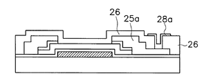
도 4는 본 발명의 일실시예에 따른 패트 부위를 나타낸 단면도Figure 4 is a cross-sectional view showing the pad portion according to an embodiment of the present invention
<도면의 주요 부분에 대한 부호의 설명><Explanation of symbols for the main parts of the drawings>
100 : 기판 101 : 게이트 전극100
102 : 게이트 절연막 103 : 반도체층102 gate
104a : 에치 스토퍼 패턴 105 : 콘택홀104a: etch stopper pattern 105: contact hole
106 : n+ 반도체층 107a : 보호막106: n + semiconductor layer 107a: protective film
본 발명은 박막 트랜지스터(Thin Film Transistor : TFT)의 제조방법에 관한 것으로, 특히 박막 트랜지스터의 성능 및 생산성을 향상시킬 수 있는 박막 트랜지스터의 제조방법에 관한 것이다.The present invention relates to a method of manufacturing a thin film transistor (TFT), and more particularly, to a method of manufacturing a thin film transistor capable of improving the performance and productivity of the thin film transistor.
근래에 고품위 TV(high definition TV : HDTV) 등의 새로운 첨단 영상기기가 개발됨에 따라 평판 표시기에 대한 요구가 대두되고 있다. LCD는 평판 표시기의 대표적인 기술로써 ELD(Electro Luminescence Display), VFD(Vacuum Fluorescence Display), PDP(Plasma Display Panel) 등이 해결하지 못한 저전력화, 고속화 등의 문제를 가지고 있지 않다.Recently, with the development of new high-tech video devices such as high definition TVs (HDTVs), there is a demand for flat panel displays. LCD is a representative technology of flat panel display and does not have problems such as low power and high speed which ELD (Electro Luminescence Display), VFD (Vacuum Fluorescence Display) and PDP (Plasma Display Panel) cannot solve.
이와 같은 LCD는 크게 수동형과 능동형의 두 가지 형태로 나누어지는데, 능동형 LCD는 각 화소 하나 하나를 박막트랜지스터와 같은 능동소자가 제어하도록 되어 있어 속도, 시야각 그리고 대조비(contrast)에 있어서, 수동형 LCD보다 훨씬 뛰어나 100만 화소 이상의 해상도를 필요로 하는 HDTV에 가장 적합한 표시기로 사용되고 있다. 이에 따라, TFT의 중요성이 부각되면서 이에 대한 연구개발이 심화되고 있다.These LCDs are divided into two types, passive and active. Active LCDs are controlled by active elements such as thin film transistors so that each pixel is controlled in terms of speed, viewing angle, and contrast. It is used as the best indicator for HDTV that requires excellent resolution of 1 million pixels or more. Accordingly, as the importance of TFTs is highlighted, R & D on them is intensifying.
현재 LCD 등에서 화소전극의 선택적 구동을 위해 전기적 스위칭 소자로 사용되는 TFT에 대한 연구개발은 수율 향상 및 생산성 개선에 의한 제조 코스트의 절감에 초점을 맞추어 TFT의 구조개선, 비정질 또는 다결정 실리콘의 특성향상, 전극의 오옴성 접촉저항 및 단선/단락 방지 등에 집중되고 있다. 이중, 비정질 실리콘 TFT의 기술은 대면적, 저가격, 양산성을 이유로 더 많은 연구가 이루어지고 있다. Currently, research and development on TFTs, which are used as electrical switching elements for selective driving of pixel electrodes in LCDs, focus on improving the structure of TFTs, improving the characteristics of amorphous or polycrystalline silicon, The focus is on ohmic contact resistance of electrodes and prevention of disconnection and short circuit. Of these, more research is being conducted on the technology of amorphous silicon TFT because of its large area, low cost, and mass productivity.
일반적으로 제조라인에서 사용되는 비정질 TFT는 게이트의 구조에 따라 크게 두 종류로 나누어진다. 그 하나는 역 스택형이라고도 불리 우는 바텀 게이트(bottom gate)형이며, 다른 하나는 정 스택형이라고도 불리 우는 탑 게이트(top gate)형이다. In general, amorphous TFTs used in manufacturing lines are largely divided into two types depending on the structure of the gate. One is a bottom gate type, also called reverse stack type, and the other is a top gate type, also called forward stack type.
상기 바텀 게이트형은 기판 상에 게이트 전극을 먼저 형성하는 것으로 주종을 이루고 있다. 한편, 탑 게이트형은 최초에 박막 트랜지스터의 소오스/드레인 전극을 형성하는 것으로, 현실적으로 누설전류가 크고 양산성이 결여되는 등의 이유로 많이 사용되지 않고 있다.The bottom gate type is mainly formed by first forming a gate electrode on a substrate. On the other hand, the top gate type first forms the source / drain electrodes of the thin film transistor, and is not used much because of the fact that the leakage current is large and the productivity is not sufficient.
상기 바텀 게이트형은 다시 두 종류로 구분된다. 그 하나는 BCE(Back Channel Etch) 타입의 TFT이고, 다른 하나는 ES(Etch Stopper) 타입의 TFT이다.The bottom gate type is divided into two types. One is TFT of BCE (Back Channel Etch) type and the other is TFT of ES (Etch Stopper) type.
이하, 첨부된 도면을 참조하여 종래의 박막 트랜지스터의 제조방법에 대하여 설명하기로 한다.Hereinafter, a manufacturing method of a conventional thin film transistor will be described with reference to the accompanying drawings.
도 1a 내지 도 1f는 종래의 ES 타입의 박막 트랜지스터의 제조방법을 나타낸 공정 단면도이다.1A to 1F are cross-sectional views illustrating a method of manufacturing a conventional ES type thin film transistor.
도 1a에 도시한 바와 같이 투명한 하부 절연 기판(10)상에 제 1 마스크를 이용하여 게이트 전극(11)을 형성하고, 상기 게이트 전극(11)을 포함한 기판(10) 전면에 게이트 절연막(12)과 비정질 실리콘층(13)을 차례로 증착한다.As shown in FIG. 1A, the
도 1b에 도시한 바와 같이 상기 비정질 실리콘층(13)상에 SiNX 재질의 에치 스토퍼층(14)을 증착한 후, 제 2 마스크를 이용한 식각공정을 통해 상기 에치 스토 퍼층(14)을 선택적으로 제거하여 에치 스토퍼 패턴(14a)을 형성한다.As illustrated in FIG. 1B, an etch stopper layer 14 of SiN X material is deposited on the
도 1c에 도시한 바와 같이 상기 기판(10) 전면을 HF 용액으로 세정하고, 상기 에치 스토퍼 패턴(14a)을 포함한 게이트 절연층(12)상에 PECVD(Plasma Enhanced Chemical Vapor Deposition) 공정으로 n+ 비정질 실리콘층이나 미세 결정질 실리콘층(15)을 증착한다.As shown in FIG. 1C, the entire surface of the substrate 10 is cleaned with an HF solution, and n + amorphous on the
그리고 제 3 마스크를 이용한 식각공정을 통해 비정질 실리콘(13)과 n+ 비정질 실리콘층이나 미세 결정질 실리콘층(15)을 제거하여 반도체층(13a)과 n+ 반도체층(15a)을 형성한다.The
이어, 도면에는 도시하지 않았지만 제 4 마스크를 이용한 식각공정을 통해 패드부위의 게이트 전극이 소정부분 노출되도록 콘택홀을 형성한다.Next, although not shown in the drawing, a contact hole is formed to expose a predetermined portion of the gate electrode on the pad portion through an etching process using a fourth mask.
도 1d에 도시한 바와 같이 상기 n+ 반도체층(115a)을 포함한 게이트 절연막(12)상에 ITO층(16)을 증착하고, 제 5 마스크를 이용한 식각공정을 통해 상기 ITO층(16)을 선택적으로 제거하여 상기 게이트 절연막(12)상에 화소전극(16a)을 형성한다.As shown in FIG. 1D, the ITO layer 16 is deposited on the
도 1e에 도시한 바와 같이 상기 화소전극(16a)을 포함한 전면에 스퍼터닝 공정으로 금속층(17)을 증착한 후, 제 6 마스크를 이용한 식각 공정으로 상기 에치 스토퍼 패턴(14a)이 소정부분 노출되도록 상기 금속층(17)과 n+ 반도체층(5a)을 선택적으로 제거하여 소오스/드레인 전극(17a)을 형성한다.
As shown in FIG. 1E, the metal layer 17 is deposited on the entire surface including the
도 1f에 도시한 바와 같이 상기 소오스/드레인 전극(17a)을 포함한 기판(10) 전면에 보호층(18)을 증착하고, 제 7 마스크를 이용한 식각공정을 이용하여 보호층 패턴(18)을 형성한다. 이때, 상기 보호층(18)은 PVX이다.As shown in FIG. 1F, the
여기서, 상기 ES 타입은 백 채널(Back Channel)부의 열화 요소가 없어 TFT 특성면에서 우수하고, 반도체층으로 이용되는 비정질 실리콘을 얇게 형성할 수 있다.Here, the ES type is excellent in TFT characteristics because there is no deterioration element in the back channel portion, and thus, an amorphous silicon used as a semiconductor layer can be formed thinly.
도 2a 내지 도 2d는 종래의 BCE 타입의 박막 트랜지스터의 제조방법을 나타낸 공정 단면도이다.2A to 2D are cross-sectional views illustrating a method of manufacturing a conventional BCE type thin film transistor.
도 2a에 도시한 바와 같이 투명한 하부 절연 기판(20)상에 제 1 마스크를 이용하여 게이트 전극(21)을 형성하고, 상기 게이트 전극(21)을 포함한 기판(20) 전면에 제 2 마스크를 이용한 식각 공정을 이용하여 게이트 절연층(22), 비정질 실리콘 재질의 반도체층(23)과 n+ 반도체층(예컨대, n+ 비정질 실리콘층이나 미세 결정질 실리콘층)(24)을 순차적으로 증착한다. 이때, 상기 n+ 반도체층(24)은 PECVD 공정을 이용한다.As shown in FIG. 2A, the
도 2b에 도시한 바와 같이 상기 n+ 반도체층(24)상에 금속층(25)을 증착한 후, 제 3 마스크를 이용하여 상기 금속층(25)을 식각하여 소오스/드레인 전극(25a)을 형성한다. 그리고 상기 반도체층(23)이 소정부분 노출되도록 n+ 반도체층(24)을 선택적으로 제거한다.
As shown in FIG. 2B, after depositing the metal layer 25 on the n + semiconductor layer 24, the metal layer 25 is etched using a third mask to form a source /
도 2c에 도시한 바와 같이 상기 소오스/드레인 전극(25a)을 포함한 기판(10) 전면에 보호층(26)을 증착한 후, 제 4 마스크를 이용하여 상기 소오스/드레인 전극(25a)중 어느 하나가 소정부분 노출되도록 보호층(26)을 제거하여 콘택홀(27)을 형성한다.As shown in FIG. 2C, after the
도 2d에 도시한 바와 같이 상기 콘택홀(27)을 포함한 보호층(26)상에 ITO(28)을 증착한 후, 제 5 마스크를 이용하여 상기 보호층(26)상의 소정부분에 픽셀 전극(28a)을 형성한다.As shown in FIG. 2D, the ITO 28 is deposited on the
따라서, BCE 타입은 제 5 마스크 공정을 이용하므로 생산성 측면에서 ES 타입보다 우수하다.Therefore, the BCE type is superior to the ES type in terms of productivity since it uses the fifth mask process.
그러나 상기와 같은 박막 트랜지스터의 제조방법에 있어서는 다음과 같은 문제점이 있었다.However, the manufacturing method of the thin film transistor as described above has the following problems.
ES 타입의 박막 트랜지스터는 7개의 마스크를 이용하여 공정을 진행하므로 공정 수가 늘고, 공정 진행상의 여러 가지 문제점으로 인해 양산 기술로 적용하는데 많은 제약이 있다.Since the ES type thin film transistor processes the process using seven masks, the number of processes increases, and there are many limitations in application to the mass production technology due to various problems in the process progress.
그리고 BCE 타입의 박막 트랜지스터는 제 5 마스크 공정을 이용하므로 에치 스토퍼 타입의 박막 트랜지스터보다 생산성 측면에서 우수한 장점이 있으나 n+ 반도체층 식각시 백 채널부위의 반도체층으로 이용되는 비정질 실리콘이 열화되므로 박막 트랜지스터의 성능이 떨어진다. And since the BCE type thin film transistor uses the fifth mask process, there is an advantage in terms of productivity compared to the etch stopper type thin film transistor, but since the amorphous silicon used as the semiconductor layer of the back channel portion during n + semiconductor layer etching is degraded Performance drops.
또한, 비정질 실리콘층의 두께를 두껍게 형성해야하므로 광투과율이 낮아 후면 노광 진행시 어려움이 있다.In addition, since the thickness of the amorphous silicon layer must be formed thick, the light transmittance is low, so that there is a difficulty in proceeding the rear exposure.
본 발명은 상기와 같은 문제점을 해결하기 위하여 안출한 것으로, ES 타입의 박막 트랜지스터 형성시 마스크 공정 수를 줄여 성능과 생산성을 향상시킬 수 있는 박막 트랜지스터의 제조방법을 제공하는데 그 목적이 있다.The present invention has been made to solve the above problems, and an object of the present invention is to provide a method of manufacturing a thin film transistor which can improve the performance and productivity by reducing the number of mask processes when forming an ES type thin film transistor.
상기와 같은 목적을 달성하기 위한 본 발명의 박막 트랜지스터의 제조방법은 기판에 게이트 전극을 형성하는 단계와, 상기 게이트 전극상에 액티브층으로서 게이트 절연막, 반도체층, 에치 스토퍼층을 순차적으로 형성하는 공정과, 상기 반도체층이 소정부분 노출되도록 에치 스토퍼층을 선택적으로 제거하여 비아홀을 형성하는 공정과, 상기 비아홀을 포함한 에치 스토퍼층상에 선택적으로 n+ 반도체층과 소오스/드레인 전극을 형성하는 전극과, 상기 소오스/드레인 전극과 연결되도록 선택적으로 픽셀 전극을 형성하는 공정을 포함하는 것을 특징으로 한다.A method of manufacturing a thin film transistor of the present invention for achieving the above object is a step of forming a gate electrode on a substrate, and sequentially forming a gate insulating film, a semiconductor layer, an etch stopper layer as an active layer on the gate electrode Selectively removing an etch stopper layer to expose a predetermined portion of the semiconductor layer to form a via hole, an electrode for selectively forming an n + semiconductor layer and a source / drain electrode on the etch stopper layer including the via hole; And selectively forming a pixel electrode to be connected to the source / drain electrode.
이하, 첨부된 도면을 참조하여 본 발명의 박막 트랜지스터의 제조방법을 나타낸 공정 단면도이다.Hereinafter, a process cross-sectional view showing a method of manufacturing a thin film transistor of the present invention with reference to the accompanying drawings.
도 3a 내지 도 3d는 본 발명의 일실시예에 따른 박막 트랜지스터의 제조방법을 나타낸 공정 단면도이고, 도 4는 본 발명의 일실시예에 따른 패트 부위를 나타낸 단면도이다.3A to 3D are cross-sectional views illustrating a method of manufacturing a thin film transistor according to an exemplary embodiment of the present invention, and FIG. 4 is a cross-sectional view illustrating a pad portion according to an exemplary embodiment of the present invention.
도 3a에 도시한 바와 같이 투명한 하부 절연 기판(100)상에 제 1 마스크를 이용하여 게이트 전극(101)을 형성하고, 상기 게이트 전극(101)을 포함한 기판(100) 전면에 제 2 마스크를 이용하여 액티브층으로서 게이트 절연막(102), 비정질 실리콘 재질의 반도체층(103) 그리고 PVX 재질의 에치 스토퍼층(104)을 순차적으로 형성한다. 이때, 도면에는 도시하지 않았지만 오밋 콘택(Ohmi Contact) 부분만을 제외하고 상기 PVX 재질의 에치 스토퍼층(104) 형성하므로 채널 부위를 평탄화할 수 있다.As shown in FIG. 3A, the
도 3b에 도시한 바와 같이 상기 에치 스토퍼층(104)에 제 3 마스크를 이용하여 후면 노광 공정을 통해 상기 반도체층(103)이 소정부분 노출되도록 콘택홀(105)을 형성함과 동시에 에치 스토퍼 패턴(104a)을 형성한다. 이때, 상기 에치 스토퍼층(104)은 습식식각 공정을 이용하여 선택적으로 제거한다.As shown in FIG. 3B, a
한편, 도 4에 도시한 바와 같이 패드 부위는 게이트 전극(101)과 후 공정에서 형성될 ITO 재질의 픽셀 전극(108a)을 콘택시킨다.Meanwhile, as shown in FIG. 4, the pad portion contacts the
도 3c에 도시한 바와 같이 상기 기판(100) 전면에 HF 용액으로 세정한 후, 상기 콘택홀(105)을 포함한 에치 스토퍼 패턴(104a)상에 n+ 반도체층(106)을 증착하고, 상기 n+ 반도체층(106)상에 금속배선층(107)을 순차적으로 증착한다.As shown in FIG. 3C, the entire surface of the
이어, 상기 n+ 반도체층(106)과 금속배선층(107)에 제 4 마스크 공정을 이용하여 상기 에치 스토퍼 패턴(104a)이 선택적으로 소정부분 노출되도록 상기 금속배선층(107)과 n+ 반도체층(106)을 동시에 식각하여 소오스/드레인 전극(107a)을 형성 하고, 상기 반도체층(103)의 양 에지부상에 n+ 반도체층(106)을 형성한다.Then, the n + semiconductor layer 106 and the metal wiring layer 107, a fourth mask process using the etch stopper pattern (104a) is selective to the metal wiring layer 107 to expose a predetermined portion of the n + semiconductor layer ( 106 is simultaneously etched to form source /
도 3d에 도시한 바와 같이 상기 소오스/드레인 전극(107a)을 포함한 기판(100) 전면에 ITO(108)을 증착하고, 제 5 마스크 공정을 이용하여 상기 ITO(108)를 선택적으로 제거하여 상기 소오스/드레인 전극(107a)상의 소정부분에 픽셀 전극(108a)을 형성한다.As shown in FIG. 3D, an ITO 108 is deposited on the entire surface of the
이상에서 설명한 바와 같이 본 발명의 박막 트랜지스터의 제조방법에 의하면, 에치 스토퍼 패턴 형성시 콘택 부위를 동시에 형성하므로 5개 마스크를 이용한 ES 타입의 박막 트랜지스터를 형성할 수 있다.As described above, according to the method of manufacturing the thin film transistor of the present invention, since the contact portion is formed at the time of forming the etch stopper pattern, an ES type thin film transistor using five masks can be formed.
따라서, 5개의 마스크를 이용하여 에치 스토퍼를 형성하므로 BEC 타입에서 발생하는 백 채널의 열화 포커스를 제거할 수 있고, 박막 트랜지스터의 특성을 향상시킬 수 있다.Therefore, since the etch stopper is formed using five masks, the deterioration focus of the back channel generated in the BEC type can be eliminated, and the characteristics of the thin film transistor can be improved.
또한, 채널부위의 오밋 콘택 부위를 제외한 부분에 PVX 재질을 형성하여 기판을 평탄화할 수 있어 박막 트랜지스터의 성능을 향상시킬 수 있다.In addition, the substrate may be planarized by forming a PVX material on a portion other than the ohmic contact portion of the channel portion, thereby improving performance of the thin film transistor.
그리고 에치 스토퍼 형성으로 인해 반도체층으로 이용되는 비정질 실리콘의 두께를 감소시킬 수 있으므로 광투과율을 향상시킬 수 있다.In addition, since the thickness of the amorphous silicon used as the semiconductor layer may be reduced due to the formation of the etch stopper, light transmittance may be improved.
또한, 종래의 ES 타입의 박막 트랜지스터보다 공정 수를 감소시키므로 생산성을 향상시킬 수 있고, 소오스/드레인 전극상에 선택적으로 ITO 재질을 사용하므로 데이터 오픈(Data Open)을 방지할 수 있다.In addition, productivity can be improved by reducing the number of processes compared to the conventional ES type thin film transistor, and data open can be prevented by selectively using an ITO material on the source / drain electrodes.
Claims (3)
Priority Applications (1)
| Application Number | Priority Date | Filing Date | Title |
|---|---|---|---|
| KR1020010017167A KR100809750B1 (en) | 2001-03-31 | 2001-03-31 | Manufacturing Method of Thin Film Transistor |
Applications Claiming Priority (1)
| Application Number | Priority Date | Filing Date | Title |
|---|---|---|---|
| KR1020010017167A KR100809750B1 (en) | 2001-03-31 | 2001-03-31 | Manufacturing Method of Thin Film Transistor |
Publications (2)
| Publication Number | Publication Date |
|---|---|
| KR20020076932A KR20020076932A (en) | 2002-10-11 |
| KR100809750B1 true KR100809750B1 (en) | 2008-03-04 |
Family
ID=27699479
Family Applications (1)
| Application Number | Title | Priority Date | Filing Date |
|---|---|---|---|
| KR1020010017167A Expired - Lifetime KR100809750B1 (en) | 2001-03-31 | 2001-03-31 | Manufacturing Method of Thin Film Transistor |
Country Status (1)
| Country | Link |
|---|---|
| KR (1) | KR100809750B1 (en) |
Cited By (5)
| Publication number | Priority date | Publication date | Assignee | Title |
|---|---|---|---|---|
| KR20100091469A (en) * | 2009-02-10 | 2010-08-19 | 삼성전자주식회사 | Thin film transistor array panel and manufacturing method thereof |
| US8519393B2 (en) | 2009-12-10 | 2013-08-27 | Samsung Display Co., Ltd. | Thin film transistor array panel and manufacturing method thereof |
| US8614443B2 (en) | 2011-02-17 | 2013-12-24 | Samsung Display Co., Ltd. | Display apparatus and method of manufacturing the same |
| CN103872061A (en) * | 2012-12-10 | 2014-06-18 | 乐金显示有限公司 | Array substrate and method of fabricating the same |
| US9093540B2 (en) | 2012-06-04 | 2015-07-28 | Samsung Display Co., Ltd. | Oxide semicondutor thin film transistor |
Citations (4)
| Publication number | Priority date | Publication date | Assignee | Title |
|---|---|---|---|---|
| JPH0269942A (en) * | 1988-09-05 | 1990-03-08 | Nec Corp | Ultrathin film transistor and manufacture thereof |
| JPH07312426A (en) * | 1994-05-18 | 1995-11-28 | Casio Comput Co Ltd | Thin film transistor and manufacturing method thereof |
| JPH0870002A (en) * | 1994-08-29 | 1996-03-12 | Nec Corp | Semiconductor device and manufacturing method thereof |
| JPH10294323A (en) * | 1997-04-22 | 1998-11-04 | Fujitsu Ltd | Method for manufacturing semiconductor device |
-
2001
- 2001-03-31 KR KR1020010017167A patent/KR100809750B1/en not_active Expired - Lifetime
Patent Citations (4)
| Publication number | Priority date | Publication date | Assignee | Title |
|---|---|---|---|---|
| JPH0269942A (en) * | 1988-09-05 | 1990-03-08 | Nec Corp | Ultrathin film transistor and manufacture thereof |
| JPH07312426A (en) * | 1994-05-18 | 1995-11-28 | Casio Comput Co Ltd | Thin film transistor and manufacturing method thereof |
| JPH0870002A (en) * | 1994-08-29 | 1996-03-12 | Nec Corp | Semiconductor device and manufacturing method thereof |
| JPH10294323A (en) * | 1997-04-22 | 1998-11-04 | Fujitsu Ltd | Method for manufacturing semiconductor device |
Cited By (9)
| Publication number | Priority date | Publication date | Assignee | Title |
|---|---|---|---|---|
| KR20100091469A (en) * | 2009-02-10 | 2010-08-19 | 삼성전자주식회사 | Thin film transistor array panel and manufacturing method thereof |
| KR101594471B1 (en) | 2009-02-10 | 2016-02-29 | 삼성디스플레이 주식회사 | Thin film transistor array panel and manufacturing method thereof |
| US8519393B2 (en) | 2009-12-10 | 2013-08-27 | Samsung Display Co., Ltd. | Thin film transistor array panel and manufacturing method thereof |
| US8614443B2 (en) | 2011-02-17 | 2013-12-24 | Samsung Display Co., Ltd. | Display apparatus and method of manufacturing the same |
| US9093540B2 (en) | 2012-06-04 | 2015-07-28 | Samsung Display Co., Ltd. | Oxide semicondutor thin film transistor |
| US9455333B2 (en) | 2012-06-04 | 2016-09-27 | Samsung Display Co., Ltd. | Thin film transistor array panel |
| US9793377B2 (en) | 2012-06-04 | 2017-10-17 | Samsung Display Co., Ltd. | Thin film transistor, thin film transistor array panel including the same, and manufacturing method thereof |
| USRE48290E1 (en) | 2012-06-04 | 2020-10-27 | Samsung Display Co., Ltd. | Thin film transistor array panel |
| CN103872061A (en) * | 2012-12-10 | 2014-06-18 | 乐金显示有限公司 | Array substrate and method of fabricating the same |
Also Published As
| Publication number | Publication date |
|---|---|
| KR20020076932A (en) | 2002-10-11 |
Similar Documents
| Publication | Publication Date | Title |
|---|---|---|
| US7071037B2 (en) | Semiconductor device and manufacturing method thereof | |
| KR101282897B1 (en) | Poly Silicon Thin Film Transistor and Method of fabricating the same | |
| JP2008140984A (en) | Semiconductor device, method for manufacturing semiconductor device, and display device | |
| US6757031B2 (en) | Metal contact structure and method for thin film transistor array in liquid crystal display | |
| JP2019537282A (en) | Array substrate, method of manufacturing the same, and display device | |
| KR101134989B1 (en) | Method of fabricating array substrate | |
| US8093113B2 (en) | Array substrate for LCD and method of fabrication thereof | |
| US7125756B2 (en) | Method for fabricating liquid crystal display device | |
| KR20110058356A (en) | Array substrate and its manufacturing method | |
| KR101246790B1 (en) | Array substrate and method of fabricating the same | |
| KR100809750B1 (en) | Manufacturing Method of Thin Film Transistor | |
| US7414691B2 (en) | Liquid crystal display device with prevention of defective disconnection of drain/pixel electrodes by forming two conductive layers on top of entire pixel electrode and then removing a portion of both therefrom | |
| KR20120067108A (en) | Array substrate and method of fabricating the same | |
| KR100539583B1 (en) | Method for crystallizing Silicon and method for manufacturing Thin Film Transistor (TFT) using the same | |
| JP2556550B2 (en) | Method for forming high yield electrical contacts to amorphous silicon | |
| KR100494705B1 (en) | A method for manufacturing of tft lcd | |
| KR100390457B1 (en) | A structure of thin film transistor and a method for manufacturing the same | |
| KR100837884B1 (en) | Manufacturing method of liquid crystal display device | |
| KR100525437B1 (en) | Liquid crystal display device and method for fabricating the same | |
| KR100208023B1 (en) | Method of manufacturing thin film transistor | |
| KR100476049B1 (en) | A method for manufacturing of storage capacitor of liquid crystal display | |
| KR100242946B1 (en) | Thin film transistor and its manufacturing method | |
| KR100816563B1 (en) | Manufacturing Method of Thin Film Transistor | |
| KR19980072230A (en) | Method of manufacturing thin film transistor | |
| KR19990016120A (en) | Thin film transistor and its manufacturing method |
Legal Events
| Date | Code | Title | Description |
|---|---|---|---|
| PA0109 | Patent application |
Patent event code: PA01091R01D Comment text: Patent Application Patent event date: 20010331 |
|
| N231 | Notification of change of applicant | ||
| PN2301 | Change of applicant |
Patent event date: 20011009 Comment text: Notification of Change of Applicant Patent event code: PN23011R01D |
|
| PG1501 | Laying open of application | ||
| N231 | Notification of change of applicant | ||
| PN2301 | Change of applicant |
Patent event date: 20030228 Comment text: Notification of Change of Applicant Patent event code: PN23011R01D |
|
| A201 | Request for examination | ||
| PA0201 | Request for examination |
Patent event code: PA02012R01D Patent event date: 20060125 Comment text: Request for Examination of Application Patent event code: PA02011R01I Patent event date: 20010331 Comment text: Patent Application |
|
| E902 | Notification of reason for refusal | ||
| PE0902 | Notice of grounds for rejection |
Comment text: Notification of reason for refusal Patent event date: 20070525 Patent event code: PE09021S01D |
|
| E701 | Decision to grant or registration of patent right | ||
| PE0701 | Decision of registration |
Patent event code: PE07011S01D Comment text: Decision to Grant Registration Patent event date: 20071126 |
|
| GRNT | Written decision to grant | ||
| PR0701 | Registration of establishment |
Comment text: Registration of Establishment Patent event date: 20080226 Patent event code: PR07011E01D |
|
| PR1002 | Payment of registration fee |
Payment date: 20080226 End annual number: 3 Start annual number: 1 |
|
| PG1601 | Publication of registration | ||
| G170 | Re-publication after modification of scope of protection [patent] | ||
| PG1701 | Publication of correction | ||
| PR1001 | Payment of annual fee |
Payment date: 20101216 Start annual number: 4 End annual number: 4 |
|
| PR1001 | Payment of annual fee |
Payment date: 20111229 Start annual number: 5 End annual number: 5 |
|
| FPAY | Annual fee payment |
Payment date: 20130107 Year of fee payment: 6 |
|
| PR1001 | Payment of annual fee |
Payment date: 20130107 Start annual number: 6 End annual number: 6 |
|
| FPAY | Annual fee payment |
Payment date: 20140116 Year of fee payment: 7 |
|
| PR1001 | Payment of annual fee |
Payment date: 20140116 Start annual number: 7 End annual number: 7 |
|
| FPAY | Annual fee payment |
Payment date: 20150116 Year of fee payment: 8 |
|
| PR1001 | Payment of annual fee |
Payment date: 20150116 Start annual number: 8 End annual number: 8 |
|
| FPAY | Annual fee payment |
Payment date: 20170119 Year of fee payment: 10 |
|
| PR1001 | Payment of annual fee |
Payment date: 20170119 Start annual number: 10 End annual number: 10 |
|
| FPAY | Annual fee payment |
Payment date: 20180118 Year of fee payment: 11 |
|
| PR1001 | Payment of annual fee |
Payment date: 20180118 Start annual number: 11 End annual number: 11 |
|
| FPAY | Annual fee payment |
Payment date: 20200128 Year of fee payment: 13 |
|
| PR1001 | Payment of annual fee |
Payment date: 20200128 Start annual number: 13 End annual number: 13 |
|
| PR1001 | Payment of annual fee |
Payment date: 20210126 Start annual number: 14 End annual number: 14 |
|
| PC1801 | Expiration of term |
Termination date: 20210930 Termination category: Expiration of duration |