KR100789858B1 - Method of Forming Insulating Film, Insulating Film Forming Device and Semiconductor Device - Google Patents
Method of Forming Insulating Film, Insulating Film Forming Device and Semiconductor Device Download PDFInfo
- Publication number
- KR100789858B1 KR100789858B1 KR1020067005431A KR20067005431A KR100789858B1 KR 100789858 B1 KR100789858 B1 KR 100789858B1 KR 1020067005431 A KR1020067005431 A KR 1020067005431A KR 20067005431 A KR20067005431 A KR 20067005431A KR 100789858 B1 KR100789858 B1 KR 100789858B1
- Authority
- KR
- South Korea
- Prior art keywords
- insulating film
- forming
- reactive material
- film
- chamber
- Prior art date
- Legal status (The legal status is an assumption and is not a legal conclusion. Google has not performed a legal analysis and makes no representation as to the accuracy of the status listed.)
- Expired - Fee Related
Links
Images


Classifications
-
- H—ELECTRICITY
- H10—SEMICONDUCTOR DEVICES; ELECTRIC SOLID-STATE DEVICES NOT OTHERWISE PROVIDED FOR
- H10P—GENERIC PROCESSES OR APPARATUS FOR THE MANUFACTURE OR TREATMENT OF DEVICES COVERED BY CLASS H10
- H10P14/00—Formation of materials, e.g. in the shape of layers or pillars
- H10P14/60—Formation of materials, e.g. in the shape of layers or pillars of insulating materials
- H10P14/69—Inorganic materials
- H10P14/692—Inorganic materials composed of oxides, glassy oxides or oxide-based glasses
- H10P14/6921—Inorganic materials composed of oxides, glassy oxides or oxide-based glasses containing silicon
- H10P14/6922—Inorganic materials composed of oxides, glassy oxides or oxide-based glasses containing silicon the material containing Si, O and at least one of H, N, C, F or other non-metal elements, e.g. SiOC, SiOC:H or SiONC
-
- H—ELECTRICITY
- H10—SEMICONDUCTOR DEVICES; ELECTRIC SOLID-STATE DEVICES NOT OTHERWISE PROVIDED FOR
- H10P—GENERIC PROCESSES OR APPARATUS FOR THE MANUFACTURE OR TREATMENT OF DEVICES COVERED BY CLASS H10
- H10P14/00—Formation of materials, e.g. in the shape of layers or pillars
- H10P14/60—Formation of materials, e.g. in the shape of layers or pillars of insulating materials
-
- C—CHEMISTRY; METALLURGY
- C23—COATING METALLIC MATERIAL; COATING MATERIAL WITH METALLIC MATERIAL; CHEMICAL SURFACE TREATMENT; DIFFUSION TREATMENT OF METALLIC MATERIAL; COATING BY VACUUM EVAPORATION, BY SPUTTERING, BY ION IMPLANTATION OR BY CHEMICAL VAPOUR DEPOSITION, IN GENERAL; INHIBITING CORROSION OF METALLIC MATERIAL OR INCRUSTATION IN GENERAL
- C23C—COATING METALLIC MATERIAL; COATING MATERIAL WITH METALLIC MATERIAL; SURFACE TREATMENT OF METALLIC MATERIAL BY DIFFUSION INTO THE SURFACE, BY CHEMICAL CONVERSION OR SUBSTITUTION; COATING BY VACUUM EVAPORATION, BY SPUTTERING, BY ION IMPLANTATION OR BY CHEMICAL VAPOUR DEPOSITION, IN GENERAL
- C23C16/00—Chemical coating by decomposition of gaseous compounds, without leaving reaction products of surface material in the coating, i.e. chemical vapour deposition [CVD] processes
- C23C16/22—Chemical coating by decomposition of gaseous compounds, without leaving reaction products of surface material in the coating, i.e. chemical vapour deposition [CVD] processes characterised by the deposition of inorganic material, other than metallic material
- C23C16/30—Deposition of compounds, mixtures or solid solutions, e.g. borides, carbides, nitrides
- C23C16/40—Oxides
- C23C16/401—Oxides containing silicon
-
- H—ELECTRICITY
- H10—SEMICONDUCTOR DEVICES; ELECTRIC SOLID-STATE DEVICES NOT OTHERWISE PROVIDED FOR
- H10P—GENERIC PROCESSES OR APPARATUS FOR THE MANUFACTURE OR TREATMENT OF DEVICES COVERED BY CLASS H10
- H10P14/00—Formation of materials, e.g. in the shape of layers or pillars
- H10P14/60—Formation of materials, e.g. in the shape of layers or pillars of insulating materials
- H10P14/63—Formation of materials, e.g. in the shape of layers or pillars of insulating materials characterised by the formation processes
- H10P14/6326—Deposition processes
- H10P14/6342—Liquid deposition, e.g. spin-coating, sol-gel techniques or spray coating
-
- H—ELECTRICITY
- H10—SEMICONDUCTOR DEVICES; ELECTRIC SOLID-STATE DEVICES NOT OTHERWISE PROVIDED FOR
- H10P—GENERIC PROCESSES OR APPARATUS FOR THE MANUFACTURE OR TREATMENT OF DEVICES COVERED BY CLASS H10
- H10P14/00—Formation of materials, e.g. in the shape of layers or pillars
- H10P14/60—Formation of materials, e.g. in the shape of layers or pillars of insulating materials
- H10P14/65—Formation of materials, e.g. in the shape of layers or pillars of insulating materials characterised by treatments performed before or after the formation of the materials
- H10P14/6516—Formation of materials, e.g. in the shape of layers or pillars of insulating materials characterised by treatments performed before or after the formation of the materials of treatments performed after formation of the materials
- H10P14/6529—Formation of materials, e.g. in the shape of layers or pillars of insulating materials characterised by treatments performed before or after the formation of the materials of treatments performed after formation of the materials by exposure to a gas or vapour
-
- H—ELECTRICITY
- H10—SEMICONDUCTOR DEVICES; ELECTRIC SOLID-STATE DEVICES NOT OTHERWISE PROVIDED FOR
- H10P—GENERIC PROCESSES OR APPARATUS FOR THE MANUFACTURE OR TREATMENT OF DEVICES COVERED BY CLASS H10
- H10P14/00—Formation of materials, e.g. in the shape of layers or pillars
- H10P14/60—Formation of materials, e.g. in the shape of layers or pillars of insulating materials
- H10P14/65—Formation of materials, e.g. in the shape of layers or pillars of insulating materials characterised by treatments performed before or after the formation of the materials
- H10P14/6516—Formation of materials, e.g. in the shape of layers or pillars of insulating materials characterised by treatments performed before or after the formation of the materials of treatments performed after formation of the materials
- H10P14/6548—Formation of materials, e.g. in the shape of layers or pillars of insulating materials characterised by treatments performed before or after the formation of the materials of treatments performed after formation of the materials by forming intermediate materials, e.g. capping layers or diffusion barriers
-
- H—ELECTRICITY
- H10—SEMICONDUCTOR DEVICES; ELECTRIC SOLID-STATE DEVICES NOT OTHERWISE PROVIDED FOR
- H10W—GENERIC PACKAGES, INTERCONNECTIONS, CONNECTORS OR OTHER CONSTRUCTIONAL DETAILS OF DEVICES COVERED BY CLASS H10
- H10W20/00—Interconnections in chips, wafers or substrates
- H10W20/01—Manufacture or treatment
- H10W20/071—Manufacture or treatment of dielectric parts thereof
- H10W20/074—Manufacture or treatment of dielectric parts thereof of dielectric parts comprising thin functional dielectric layers, e.g. dielectric etch-stop, barrier, capping or liner layers
- H10W20/076—Manufacture or treatment of dielectric parts thereof of dielectric parts comprising thin functional dielectric layers, e.g. dielectric etch-stop, barrier, capping or liner layers in via holes or trenches
-
- H—ELECTRICITY
- H10—SEMICONDUCTOR DEVICES; ELECTRIC SOLID-STATE DEVICES NOT OTHERWISE PROVIDED FOR
- H10W—GENERIC PACKAGES, INTERCONNECTIONS, CONNECTORS OR OTHER CONSTRUCTIONAL DETAILS OF DEVICES COVERED BY CLASS H10
- H10W20/00—Interconnections in chips, wafers or substrates
- H10W20/01—Manufacture or treatment
- H10W20/071—Manufacture or treatment of dielectric parts thereof
- H10W20/081—Manufacture or treatment of dielectric parts thereof by forming openings in the dielectric parts
-
- H—ELECTRICITY
- H10—SEMICONDUCTOR DEVICES; ELECTRIC SOLID-STATE DEVICES NOT OTHERWISE PROVIDED FOR
- H10W—GENERIC PACKAGES, INTERCONNECTIONS, CONNECTORS OR OTHER CONSTRUCTIONAL DETAILS OF DEVICES COVERED BY CLASS H10
- H10W20/00—Interconnections in chips, wafers or substrates
- H10W20/01—Manufacture or treatment
- H10W20/071—Manufacture or treatment of dielectric parts thereof
- H10W20/093—Manufacture or treatment of dielectric parts thereof by modifying materials of the dielectric parts
- H10W20/096—Manufacture or treatment of dielectric parts thereof by modifying materials of the dielectric parts by contacting with gases, liquids or plasmas
-
- H—ELECTRICITY
- H10—SEMICONDUCTOR DEVICES; ELECTRIC SOLID-STATE DEVICES NOT OTHERWISE PROVIDED FOR
- H10P—GENERIC PROCESSES OR APPARATUS FOR THE MANUFACTURE OR TREATMENT OF DEVICES COVERED BY CLASS H10
- H10P14/00—Formation of materials, e.g. in the shape of layers or pillars
- H10P14/60—Formation of materials, e.g. in the shape of layers or pillars of insulating materials
- H10P14/63—Formation of materials, e.g. in the shape of layers or pillars of insulating materials characterised by the formation processes
- H10P14/6326—Deposition processes
- H10P14/6328—Deposition from the gas or vapour phase
- H10P14/6334—Deposition from the gas or vapour phase using decomposition or reaction of gaseous or vapour phase compounds, i.e. chemical vapour deposition
- H10P14/6336—Deposition from the gas or vapour phase using decomposition or reaction of gaseous or vapour phase compounds, i.e. chemical vapour deposition in the presence of a plasma [PECVD]
-
- H—ELECTRICITY
- H10—SEMICONDUCTOR DEVICES; ELECTRIC SOLID-STATE DEVICES NOT OTHERWISE PROVIDED FOR
- H10P—GENERIC PROCESSES OR APPARATUS FOR THE MANUFACTURE OR TREATMENT OF DEVICES COVERED BY CLASS H10
- H10P14/00—Formation of materials, e.g. in the shape of layers or pillars
- H10P14/60—Formation of materials, e.g. in the shape of layers or pillars of insulating materials
- H10P14/66—Formation of materials, e.g. in the shape of layers or pillars of insulating materials characterised by the type of materials
- H10P14/665—Porous materials
-
- H—ELECTRICITY
- H10—SEMICONDUCTOR DEVICES; ELECTRIC SOLID-STATE DEVICES NOT OTHERWISE PROVIDED FOR
- H10P—GENERIC PROCESSES OR APPARATUS FOR THE MANUFACTURE OR TREATMENT OF DEVICES COVERED BY CLASS H10
- H10P14/00—Formation of materials, e.g. in the shape of layers or pillars
- H10P14/60—Formation of materials, e.g. in the shape of layers or pillars of insulating materials
- H10P14/66—Formation of materials, e.g. in the shape of layers or pillars of insulating materials characterised by the type of materials
- H10P14/668—Formation of materials, e.g. in the shape of layers or pillars of insulating materials characterised by the type of materials the materials being characterised by the deposition precursor materials
- H10P14/6681—Formation of materials, e.g. in the shape of layers or pillars of insulating materials characterised by the type of materials the materials being characterised by the deposition precursor materials the precursor containing a compound comprising Si
- H10P14/6684—Formation of materials, e.g. in the shape of layers or pillars of insulating materials characterised by the type of materials the materials being characterised by the deposition precursor materials the precursor containing a compound comprising Si the compound comprising silicon and oxygen
- H10P14/6686—Formation of materials, e.g. in the shape of layers or pillars of insulating materials characterised by the type of materials the materials being characterised by the deposition precursor materials the precursor containing a compound comprising Si the compound comprising silicon and oxygen the compound being a molecule comprising at least one silicon-oxygen bond and the compound having hydrogen or an organic group attached to the silicon or oxygen, e.g. a siloxane
Landscapes
- Chemical & Material Sciences (AREA)
- Inorganic Chemistry (AREA)
- General Chemical & Material Sciences (AREA)
- Chemical Kinetics & Catalysis (AREA)
- Engineering & Computer Science (AREA)
- Materials Engineering (AREA)
- Mechanical Engineering (AREA)
- Metallurgy (AREA)
- Organic Chemistry (AREA)
- Internal Circuitry In Semiconductor Integrated Circuit Devices (AREA)
- Chemical Vapour Deposition (AREA)
- Formation Of Insulating Films (AREA)
Abstract
CVD 장치(111)에서, 히터에 의해 반도체 웨이퍼(W)를 가열하고, 1,3,5,7-테트라메틸시클로테트라실록산(TMCTS)을 도입하여, 고주파 전압을 인가하지 않고서, 열처리를 하여, 실리콘을 포함하는 다공질 저유전률막의 개질 처리를 한다. 이어서, 동일한 CVD 장치(111)에서, 반도체 웨이퍼(W)를 가열하고, TMCTS를 도입하여, 고주파 전압을 인가하고, TMCTS를 포함하는 가스의 플라즈마를 생성하여, 다공질 저유전률막 위에 밀도·경도가 높은 절연막을 형성한다. In the CVD apparatus 111, the semiconductor wafer W is heated by a heater, 1,3,5,7-tetramethylcyclotetrasiloxane (TMCTS) is introduced, and heat treatment is performed without applying a high frequency voltage. The porous low dielectric constant film containing silicon is modified. Subsequently, in the same CVD apparatus 111, the semiconductor wafer W is heated, TMCTS is introduced, a high frequency voltage is applied, a plasma of a gas containing TMCTS is generated, and the density and hardness are applied on the porous low dielectric constant film. A high insulating film is formed.
Description
본 발명은, 다른 종류의 절연막을 효율적으로 성막할 수 있는 성막 방법과 성막 장치 등에 관한 것으로, 특히, 저유전률막의 개질과 상기 저유전률막 상에 막질이 다른 절연막을 형성하는 데에 적합한 절연막의 형성 방법과 절연막 형성 시스템에 관한 것이다.BACKGROUND OF THE INVENTION Field of the Invention The present invention relates to a film forming method and a film forming apparatus capable of forming a film of different types of insulating films efficiently, and in particular, the formation of an insulating film suitable for modifying a low dielectric constant film and forming an insulating film having a different film quality on the low dielectric constant film. A method and an insulating film forming system.
반도체 집적 회로에 있어서, 처리 속도를 향상시키기 위해서는, R·C 시상수를 저감할 필요가 있다. 저항(R)은 저항률이 낮은 구리를 배선재로서 사용함으로써 저감되며, 한편, 정전용량(C)은 층간 절연막으로서 유전률(K)이 낮은 절연막(저유전률막)을 사용함으로써 저감된다. 또한, 저유전률막을 사용함으로써, 크로스토크를 방지하는 것도 가능하게 된다. In a semiconductor integrated circuit, in order to improve the processing speed, it is necessary to reduce the R · C time constant. The resistance R is reduced by using copper having a low resistivity as the wiring material, while the capacitance C is reduced by using an insulating film having a low dielectric constant K (low dielectric constant film) as the interlayer insulating film. In addition, it is also possible to prevent crosstalk by using a low dielectric constant film.
저유전률의 절연막으로서, 내부의 빈 구멍률(空孔率)을 높인 다공질 절연막이 널리 이용되고 있다. 그러나, 다공질 절연막은 그 구조상, 일반적으로 강도가 약하고, 흡습성이 높다고 하는 문제가 있다. 그 때문에, 다공질 절연막을 소수화, 고강도화하는 개질 수법이 널리 검토되고 있다. As an insulating film having a low dielectric constant, a porous insulating film having a high internal porosity is widely used. However, the porous insulating film has a problem in that, in general, its strength is weak and its hygroscopicity is high. For this reason, modification methods for hydrophobicizing and increasing the strength of the porous insulating film have been widely studied.
1,3,5,7-테트라메틸시클로테트라실록산(1,3,5,7-Tetra Methyl Cyclo Tetra Siloxane : TMCTS)을 이용하여 플라즈마에 의한 화학 기상 성장을 행하여 SiOC막을 성막하는 기술이, 예컨대, 미국 특허 제6,147,009호 명세서에 개시되어 있다. 그러나, CVD법을 사용하는 경우, 다공질화가 곤란하기 때문에, 유전률이 매우 낮은 막을 형성하는 것이 어렵다고 하는 문제가 있다. A technique of forming a SiOC film by performing chemical vapor phase growth by plasma using 1,3,5,7-tetramethylcyclotetrasiloxane (1,3,5,7-Tetra Methyl Cyclo Tetra Siloxane: TMCTS), for example, Disclosed in US Pat. No. 6,147,009. However, when the CVD method is used, there is a problem that it is difficult to form a film having a very low dielectric constant because it is difficult to porous.
또한, 구리 배선은 다마신법에 의해, 저유전률 다공질막 상에 경도 및 밀도가 높은 하드마스크를 형성한 후, 포트리소그래프에 의해 에칭을 하여, 형성된 홈 안에 매립되어 형성된다. 또한, 홈 안에는 구리의 확산을 방지하기 위한 배리어 메탈층을 형성하여, 구리 배선을 형성하고 있다. 그러나, 다공질막에 대해서는, 배리어 메탈층 자체가 확산되어 버릴 가능성이 있다. 배선 재료의 다공질막 속으로의 확산을 방지하기 위해서 실리콘 산화막을 두는 것이, 일본 특허 공개 평9-298241호 공보에 개시되어 있다. 이하, 이 산화 실리콘막과 같은 기능, 즉, 배선 재료(금속)의 확산을 방지할 수 있는 절연막을 시일막이라고 기재한다. In addition, the copper wiring is formed by forming a hard mask having a high hardness and a high density on the low dielectric constant porous film by the damascene method, and then etching the same by using a photolithography to fill the trench. Further, a barrier metal layer for preventing the diffusion of copper is formed in the groove to form a copper wiring. However, with respect to the porous membrane, there is a possibility that the barrier metal layer itself is diffused. In order to prevent the diffusion of wiring material into the porous film, a silicon oxide film is provided in Japanese Patent Laid-Open No. 9-298241. Hereinafter, the insulating film which can prevent the function similar to this silicon oxide film, ie, the diffusion of wiring material (metal), is described as a seal film.
종래의 성막 방법에서는, 다공질막을 개질하여, 다공질막과는 막질이 다른 절연막(하드마스크나 시일막)을 더 퇴적하는 경우에는, 다른 챔버에서 다른 반응 물질을 이용하여 다공질 절연막을 개질하고, 다공질 절연막 상에 다른 절연막(하드마스크나 시일막)을 형성하고 있기 때문에, 장치 구성이 크고, 공정수가 많아져 버린다고 하는 문제가 있었다. In the conventional film forming method, when the porous film is modified to further deposit an insulating film (hard mask or seal film) having a different film quality from the porous film, the porous insulating film is modified by using a different reaction material in another chamber, and the porous insulating film Since another insulating film (hard mask or seal film) is formed on the device, there is a problem that the device configuration is large and the number of steps increases.
같은 문제는, 다공질 절연막에 한하지 않고, 저유전률막을 개질하고, 그 위에 막질이 상이한 다른 절연막(하드마스크, 시일막, 패시베이션막) 등을 형성하는 경우에도 발생하고 있었다. The same problem has arisen not only in the case of a porous insulating film, but also in the case of modifying a low dielectric constant film and forming another insulating film (hard mask, seal film, passivation film) or the like on which the film quality is different.
본 발명은 상기한 실상을 감안하여 이루어진 것으로, 저유전률막을 개질하는 처리와, 개질한 후의 저유전률막 상에 막질이 상이한 다른 절연막을 형성하는 처리를 효율적으로 실행할 수 있도록 하는 것을 목적으로 한다. This invention is made | formed in view of the above-mentioned fact, and an object of this invention is to make it possible to efficiently perform the process which reforms a low dielectric constant film, and the process which forms another insulating film from a film quality on the low dielectric constant film after reforming efficiently.
상기 목적을 달성하기 위해서, 본 발명의 제1 관점에 따른 절연막의 형성 방법은, In order to achieve the above object, the insulating film forming method according to the first aspect of the present invention,
제1 절연막을 반응성 물질을 포함하는 분위기 속에서 가열하는 열처리 공정과, A heat treatment step of heating the first insulating film in an atmosphere containing a reactive material,
상기 반응성 물질을 포함하는 가스를 이용한 화학 기상 성장(CVD)에 의해, 상기 열처리 공정에서 열처리된 상기 제1 절연막 상에, 제2 절연막을 형성하는 성막 공정을 구비하는 것을 특징으로 한다. And a film forming step of forming a second insulating film on the first insulating film heat-treated in the heat treatment step by chemical vapor deposition (CVD) using a gas containing the reactive material.
상기 방법에 있어서, 성막 공정은 예컨대, 열처리 공정에서 반응성 물질을 여기하는 것보다도 높은 에너지로 상기 반응성 물질을 여기함으로써, 화학 기상 성장을 일으키는 공정으로 구성된다. In the above method, the film forming step is configured to cause chemical vapor growth by, for example, exciting the reactive material with a higher energy than exciting the reactive material in the heat treatment step.
상기 방법에 있어서, 예컨대, 열처리 공정에서는, 실질적으로 플라즈마를 포함하지 않는 분위기 속에서 제1 절연막이 열처리되고, 성막 공정에서는, 상기 반응성 물질을 포함하는 가스의 플라즈마를 생성하여, 화학 기상 성장(CVD)을 한다. In the above method, for example, in the heat treatment step, the first insulating film is heat-treated in an atmosphere substantially free of plasma, and in the film formation step, a plasma of a gas containing the reactive material is generated and chemical vapor deposition (CVD) is performed. )
상기 방법에 있어서, 예컨대, 제1 절연막은, 다공질 절연막으로 구성되며, 열처리 공정은, 상기 반응성 물질을 다공질 절연막에 결합시켜 상기 다공질 절연막을 개질하는 개질 공정으로 구성되고, 성막 공정은, 상기 반응성 물질을 포함하는 분위기 속에 개질된 제1 절연막을 배치하고, 상기 제1 절연막을 가열하는 동시에 상기 반응성 물질을 포함하는 가스의 플라즈마를 생성하여, 상기 제1 절연막 상에서 상기 반응성 물질을 화학 기상 성장시키는 공정으로 구성된다. In the above method, for example, the first insulating film is composed of a porous insulating film, and the heat treatment step is composed of a modifying step of modifying the porous insulating film by bonding the reactive material to the porous insulating film, and the film forming step is the reactive material. Disposing a modified first insulating film in an atmosphere including a gas, heating the first insulating film, and simultaneously generating a plasma of a gas including the reactive material, thereby chemically vapor-growing the reactive material on the first insulating film. It is composed.
상기 반응성 물질은 예컨대, 상온 상압력에서 기체 또는 상온에서의 증기압이 1 Pa∼101.3 kPa, 바람직하게는 100 Pa∼101.3 kPa인 반응성 물질로 구성된다. The reactive material is composed of, for example, a reactive material having a gas at room temperature and a normal pressure, or a vapor pressure at room temperature of 1 Pa to 101.3 kPa, preferably 100 Pa to 101.3 kPa.
또한, 예컨대, 상기 반응성 물질은 실리콘과 수소를 함유하는 물질로 구성된다. 이 경우, 상기 반응성 물질은 실리콘과 수소의 결합을 2 이상 포함하는 물질로 구성되는 것이 바람직하다. Also, for example, the reactive material is composed of a material containing silicon and hydrogen. In this case, the reactive material is preferably composed of a material containing two or more bonds of silicon and hydrogen.
또한, 상기 반응성 물질은 실리콘 원자의 수가 1∼30, 또한 수소, 산소, 질소로부터 얻어지는 원소를 함유하는 물질로 구성되는 것이 바람직하다. Moreover, it is preferable that the said reactive substance is comprised from the substance containing the number of silicon atoms 1-30, and the element obtained from hydrogen, oxygen, and nitrogen.
또한, 상기 반응성 물질은 예컨대, In addition, the reactive material is, for example,

(식에서, R11, R12, R13, R14, R15, R16은 동일하더라도 다르더라도 좋으며, 각각 H, OH, C6H5, CaH2a+1, CbH2b+1, CF3(CF2)c(CH2)d, CeH2e-1 또는 할로겐 원자를 나타내고, a는 1∼3의 정수, b는 1∼3의 정수, c는 0∼10의 정수, d는 0∼4의 정수, e는 2∼4의 정수, L은 0∼8의 정수, m은 0∼8의 정수, n은 0∼8의 정수이며, 또한 3≤L+m+n≤8 임)으로 나타내어지는 적어도 1종의 환상 실록산으로 구성된다. (Wherein R 11 , R 12 , R 13 , R 14 , R 15 , R 16 may be the same or different, respectively, H, OH, C 6 H 5 , C a H 2a + 1 , C b H 2b + 1 , CF 3 (CF 2 ) c (CH 2 ) d , C e H 2e-1 or a halogen atom, a is an integer of 1 to 3, b is an integer of 1 to 3, c is an integer of 0 to 10, d is an integer of 0-4, e is an integer of 2-4, L is an integer of 0-8, m is an integer of 0-8, n is an integer of 0-8, and 3 <= L + m + n <= 8) at least one cyclic siloxane.
한편, 상기 반응성 물질은 이들에 한정되지 않고, 예컨대, In addition, the said reactive substance is not limited to these, For example,
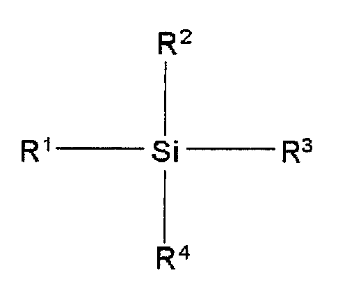
(식에서, R1, R2, R3, R4는 동일하더라도 다르더라도 좋으며, 각각 H, OH, C6H5, CaH2a+1, CbH2b+1O, CF3(CF2)c(CH2)d, CeH2e-1 또는 할로겐 원자를 나타내고, a는 1∼3의 정수, b는 1∼3의 정수, c는 0∼10의 정수, d는 0∼4의 정수, e는 2∼4의 정수임)로 나타내어지는 적어도 1종의 규소 화합물로 구성되는 것도 사용 가능하다. (Wherein R 1 , R 2 , R 3 , R 4 may be the same or different, respectively, H, OH, C 6 H 5 , C a H 2a + 1 , C b H 2b + 1 O, CF 3 (CF 2 ) c (CH 2 ) d , C e H 2e-1 or a halogen atom, a is an integer of 1 to 3, b is an integer of 1 to 3, c is an integer of 0 to 10, and d is 0 to 4 And an integer of 2 to 4 are each an integer consisting of at least one silicon compound represented by).
또한, 상기 반응성 물질은 예컨대, In addition, the reactive material is, for example,

(식에서, R5, R6, R7, R8, R9, R10은 동일만하더라도 다르더라도 좋으며, 각각 H, OH, C6H5, CaH2a+1, CbH2b+1O, CF3(CF2)c(CH2)d, CeH2e-1 또는 할로겐 원자를 나타내고, a는 1∼3의 정수, b는 1∼3의 정수, c는 0∼10의 정수, d는 0∼4의 정수, e는 2∼4의 정수임)로 나타내어지는 적어도 1종의 규소 화합물로 구성되는 것도 사용 가능하다. (Wherein R 5 , R 6 , R 7 , R 8 , R 9 , R 10 may be the same or different, respectively, H, OH, C 6 H 5 , C a H 2a + 1 , C b H 2b + 1 O, CF 3 (CF 2 ) c (CH 2) d, C e H 2e-1 or a halogen atom, a is an integer of 1~3, b is an integer of 1~3, c is of from 0 to 10 Integer, d is an integer of 0-4, e is an integer of 2-4), and it is also possible to use the thing comprised from the at least 1 sort (s) of silicon compound.
또한, 상기 반응성 물질은 예컨대, In addition, the reactive material is, for example,

(식에서, R17, R18, R19, R20, R21, R22는 동일만하더라도 다르더라도 좋으며, 각각 H, OH, C6H5, CaH2a+1, CbH2b+1O, CF3(CF2)c(CH2)d, CeH2e-1 또는 할로겐 원자를 나타내고, a는 1∼3의 정수, b는 1∼3의 정수, c는 0∼10의 정수, d는 0∼4의 정수, e는 2∼4의 정수이며, X는 O, (CH2)f, C6H4, (OSiR23R24)nO, OSiR25R26YSiR27R28O, 또는 NR29이고, R23, R24, R25, R26, R27, R28, R29는 서로 동일하더라도 다르더라도 좋으며, 각각 H, OH, C6H5, CaH2a+1, CbH2b+1O, CF3(CF2)c(CH2)d, CeH2e-1, 할로겐 원자 또는 OSiR30R31R32를 나타내고, a는 1∼3의 정수, b는 1∼3의 정수, c는 0∼10의 정수, d는 0∼4의 정 수, e는 2∼4의 정수, f는 1∼6의 정수, n은 1∼10의 정수이며, Y는 (CH2)m, C6H4를 나타내고, m은 1∼6의 정수이고, R30, R31, R32는 동일하더라도 다르더라도 좋으며, 각각 H 또는 CH3임)로 나타내어지는 적어도 1종의 규소 화합물로 구성되는 것도 사용 가능하다.(Wherein R 17 , R 18 , R 19 , R 20 , R 21 , R 22 may be the same or different, respectively, H, OH, C 6 H 5 , C a H 2a + 1 , C b H 2b + 1 O, CF 3 (CF 2 ) c (CH 2) d, c e H 2e-1 or a halogen atom, a is an integer of 1~3, b is an integer of 1~3, c is of from 0 to 10 integer, d is an integer of 0 to 4, e is an integer of 2~4, X is O, (CH 2) f, C 6 H 4, (OSiR 23 R 24) n O, OSiR 25 R 26 YSiR 27 R 28 O, or NR 29 , and R 23 , R 24 , R 25 , R 26 , R 27 , R 28 , and R 29 may be the same as or different from each other, and H, OH, C 6 H 5 , and C a H 2a, respectively. +1, c b H 2b + 1 O, CF 3 (CF 2) c (CH 2) d, c e H 2e-1, represents a halogen atom, or OSiR 30 R 31 R 32, a is an integer from 1 to 3 , b is an integer of 1 to 3, c is an integer of 0 to 10, d is an integer of 0 to 4, e is an integer of 2 to 4, f is an integer of 1 to 6, n is an integer of 1 to 10 , Y represents (CH 2 ) m , C 6 H 4 , m is an integer from 1 to 6, and R 30 , R 31 , R 32 are the same or different Good, it is also available which is composed of at least one kind of silicon compounds represented by H or CH 3 Im), respectively.
또한, 상기 반응성 물질은 예컨대, In addition, the reactive material is, for example,

(식에서, R33, R34, R35, R36, R37, R38, R39, R40, R41은 서로 동일하더라도 다르더라도 좋으며, 각각 H, OH, C6H5, CaH2a+1, CbH2b+1O, CF3(CF2)c(CH2)d, CeH2e-1 또는 할로겐 원자를 나타내고, a는 1∼3의 정수, b는 1∼3의 정수, c는 0∼10의 정수, d는 0∼4의 정수, e는 2∼4의 정수이며, L은 0∼8의 정수, m은 0∼8의 정수, n은 0∼8의 정수, 또한 3≤L+m+n≤8임)로 나타내어지는 적어도 1종의 환상 실라잔으로 구성되는 것도 사용 가능하다.Wherein R 33 , R 34 , R 35 , R 36 , R 37 , R 38 , R 39 , R 40 , and R 41 may be the same as or different from each other, and H, OH, C 6 H 5 , and C a H, respectively. 2a + 1, C b H 2b + 1 O, CF 3 (CF 2) c (CH 2) d, C e H 2e-1 or a halogen atom, a is an integer from 1 to 3, b is 1 to 3 C is an integer of 0-10, d is an integer of 0-4, e is an integer of 2-4, L is an integer of 0-8, m is an integer of 0-8, n is 0-8 It is also possible to use an integer composed of at least one cyclic silazane represented by 3 ≦ L + m + n ≦ 8).
또한, 상기 반응성 물질은, 예컨대, 1,3,5,7-테트라메틸시클로테트라실록산이다. In addition, the reactive substance is, for example, 1,3,5,7-tetramethylcyclotetrasiloxane.
제1 절연막은 실리콘을 포함하는 다공질 절연막으로 구성되며, 상기 반응성 물질은 1,3,5,7-테트라메틸시클로테트라실록산으로 구성되더라도 좋다. The first insulating film is composed of a porous insulating film containing silicon, and the reactive material may be composed of 1,3,5,7-tetramethylcyclotetrasiloxane.
제1 절연막은 반도체 장치의 층간 절연막을 구성하고, 제2 절연막은 제1 절연막보다도 경도와 밀도의 적어도 한 쪽이 높은 절연층을 구성할 수 있다. The first insulating film may constitute an interlayer insulating film of a semiconductor device, and the second insulating film may constitute an insulating layer having at least one of hardness and density higher than that of the first insulating film.
열처리 공정은 열처리 시간의 경과와 함께 분위기 속의 상기 반응성 물질의 평균 분자량을 (예컨대 연속적으로 단계적으로) 변화시키는 공정을 포함하더라도 좋다. The heat treatment step may include a step of changing (eg, continuously stepwise) the average molecular weight of the reactive substance in the atmosphere with the passage of the heat treatment time.
열처리 공정에 의한 처리 대상인 제1 절연막은 스핀 도포법에 의해 형성된 다공질 절연막 또는 화학 기상 성장(CVD)에 의해 형성된 다공질 절연막으로 구성되더라도 좋다. The first insulating film to be treated by the heat treatment step may be composed of a porous insulating film formed by a spin coating method or a porous insulating film formed by chemical vapor deposition (CVD).
본 발명의 제2 관점에 따른 절연막의 형성 방법은, Method for forming an insulating film according to a second aspect of the present invention,
실리콘을 포함하는 다공질막을 1,3,5,7-테트라메틸시클로테트라실록산을 포함하는 분위기 속에 배치하고 가열하여, 상기 다공질막을 개질하는 개질 공정과, A reforming process of modifying the porous membrane by placing and heating a porous membrane comprising silicon in an atmosphere containing 1,3,5,7-tetramethylcyclotetrasiloxane,
개질된 상기 다공질막을 1,3,5,7-테트라메틸시클로테트라실록산을 포함하는 분위기 속에 배치하여, 상기 1,3,5,7-테트라메틸시클로테트라실록산을 포함하는 가스를 이용한 화학 기상 성장에 의해, 상기 다공질막 상에, 상기 개질된 다공질막보다도 경도와 밀도의 적어도 한 쪽이 높은 절연막을 형성하는 성막 공정을 구비하는 것을 특징으로 한다. The modified porous membrane is placed in an atmosphere containing 1,3,5,7-tetramethylcyclotetrasiloxane, and subjected to chemical vapor growth using a gas containing the 1,3,5,7-tetramethylcyclotetrasiloxane. A film forming step of forming an insulating film having a higher hardness and a density than the modified porous film is provided on the porous film.
개질 공정에서는, 1,3,5,7-테트라메틸시클로테트라실록산을 포함하는 분위기 가스의 플라즈마를 생성시키지 않고, 성막 공정에서는, 1,3,5,7-테트라메틸시클로테트라실록산을 포함하는 가스의 플라즈마를 생성하여 화학 기상 성장을 하도록 하더라도 좋다. In the reforming step, the plasma of the atmosphere gas containing 1,3,5,7-tetramethylcyclotetrasiloxane is not generated, and in the film forming step, the gas containing 1,3,5,7-tetramethylcyclotetrasiloxane It is also possible to generate a plasma of chemical vapor deposition.
상기 목적을 달성하기 위해서, 본 발명의 제3 관점에 따른 절연막 형성 시스템은, 제1 챔버와, 상기 제1 챔버 내에 배치되어 피처리체를 지지하는 제1 지지체와, 상기 제1 지지체에 의해 지지된 피처리체를 가열하는 제1 히터와, 상기 제1 챔버 내에 소정의 반응성 물질을 포함하는 가스를 공급하는 제1 가스 공급 수단과, 제1 지지체 상에 제1 절연막이 배치된 상태에서, 상기 제1 가스 공급 수단에 의해 상기 제1 챔버 내에 상기 반응성 물질을 포함하는 가스를 도입하는 동시에 상기 제1 히터에 의해 상기 제1 절연막을 가열하는 제1 제어 수단과, 제2 챔버와, 상기 제2 챔버 내에 배치되어 피처리체를 지지하는 제2 지지체와, 상기 제2 지지체에 의해 지지된 피처리체를 가열하는 제2 히터와, 상기 제2 챔버 내에 상기 반응성 물질을 포함하는 가스를 공급하는 제2 가스 공급 수단과, 제2 지지체 상에 상기 제1 절연막이 지지된 상태에서, 상기 제2 가스 공급 수단에 의해 상기 제2 챔버 내에 상기 반응성 물질을 포함하는 가스를 도입하여, 상기 제1 절연막 상에 상기 반응 물질로부터의 생성물을 포함하는 제2 절연막을 형성하는 제2 제어 수단을 구비하는 것을 특징으로 한다. In order to achieve the above object, the insulating film forming system according to the third aspect of the present invention comprises a first chamber, a first support disposed in the first chamber to support the object to be processed, and supported by the first support. A first heater for heating the object, first gas supply means for supplying a gas containing a predetermined reactive material in the first chamber, and a first insulating film disposed on the first support, wherein the first First control means for heating the first insulating film by the first heater while introducing a gas containing the reactive material into the first chamber by a gas supply means, a second chamber, and the second chamber; A second support disposed to support the object to be processed, a second heater to heat the object to be supported by the second support, and a second to supply a gas containing the reactive material into the second chamber. In the state where the first insulating film is supported on the gas supply means and the second support, the gas containing the reactive substance is introduced into the second chamber by the second gas supply means, and the gas is supplied onto the first insulating film. And second control means for forming a second insulating film comprising a product from said reactant.
제2 챔버 내에 상기 반응성 물질을 포함하는 가스의 플라즈마를 생성하는 플라즈마 생성 수단을 더 구비하고, 제2 제어 수단은, 제2 지지체 상에 제1 절연막이 배치된 상태에서, 제2 가스 공급 수단에 의해 제2 챔버 내에 상기 반응성 물질을 포함하는 가스를 도입하여, 제2 히터에 의해 제1 절연막을 가열하고, 또한, 플라즈마 생성 수단에 의해 상기 반응성 물질을 포함하는 가스의 플라즈마를 생성함으로써, 제1 절연막 상에 상기 반응성 물질로부터의 생성물을 포함하는 제2 절연막을 형성하도록 하더라도 좋다. And a plasma generating means for generating a plasma of the gas containing the reactive material in the second chamber, wherein the second control means is connected to the second gas supply means in a state where the first insulating film is disposed on the second support. By introducing a gas containing the reactive material into the second chamber, heating the first insulating film by the second heater, and generating a plasma of the gas containing the reactive material by the plasma generating means. A second insulating film containing a product from the reactive material may be formed on the insulating film.
제1 및 제2 챔버는 물리적으로 하나의 챔버로 구성되고, 제1 및 제2 지지체는 물리적으로 하나의 지지체로 구성되며, 제1 및 제2 히터는 물리적으로 하나의 히터로 구성되고, 제1 및 제2 제어 수단은 물리적으로 공통의 제어부로 구성되며, 챔버는 상기 챔버에 도입된 가스에 고주파 전계를 인가하는 고주파 전계 인가 수단을 구비하고, 제어부는 열처리시에는 가스에 고주파 전계를 인가하지 않고, 성막시에는 고주파 전계를 인가하도록 고주파 전계 인가 수단을 제어하는 수단을 구비하며, 1대로 제1 절연막의 개질과 개질된 제1 절연막 상에의 제2 절연막의 형성이 가능하도록 하더라도 좋다. The first and second chambers are physically composed of one chamber, the first and second supports are physically composed of one support, the first and second heaters are physically composed of one heater, and the first And a second control means comprising a physically common control unit, wherein the chamber includes high frequency electric field applying means for applying a high frequency electric field to the gas introduced into the chamber, and the control unit does not apply a high frequency electric field to the gas during heat treatment. And a means for controlling the high frequency electric field applying means so as to apply a high frequency electric field at the time of film formation. The first insulating film may be modified and the second insulating film may be formed on the modified first insulating film.
도 1은 본 발명의 실시형태에 따른 성막 장치의 시스템 구성을 도시한 도면이다. 1 is a diagram illustrating a system configuration of a film forming apparatus according to an embodiment of the present invention.
도 2는 도 1에 도시한 CVD 장치의 일례를 도시한 도면이다. FIG. 2 is a diagram showing an example of the CVD apparatus shown in FIG. 1.
도 3은 본 발명의 제1 실시형태에 따른 프로세스의 레시피의 예를 도시한 도면이다.3 is a diagram showing an example of a recipe of a process according to the first embodiment of the present invention.
도 4는 본 발명의 제1 실시형태에 따른 프로세스의 공정을 설명하기 위한 결과물의 단면도이다. 4 is a cross-sectional view of the result for explaining a process of the process according to the first embodiment of the present invention.
도 5는 본 발명의 제2 실시형태에 따른 프로세스의 공정을 설명하기 위한 결과물의 단면도이다. 5 is a cross-sectional view of the result for explaining a process of the process according to the second embodiment of the present invention.
도 6은 본 발명의 제3 실시형태에 따른 프로세스의 공정을 설명하기 위한 결 과물의 단면도이다. 6 is a cross-sectional view of the result for explaining the process of the process according to the third embodiment of the present invention.
도 7은 도 1에 도시한 CVD 장치의 다른 예를 도시한 도면이다. FIG. 7 is a diagram showing another example of the CVD apparatus shown in FIG. 1.
<도면의 주요 부분에 대한 부호의 설명><Explanation of symbols for the main parts of the drawings>
11 : 성막 장치 12 : 스핀 도포실11
13 : CVD 장치 14 : 반송실13: CVD apparatus 14: conveyance chamber
15 : 반입출실 17 : 반송 아암15: carrying in and out 17: return arm
100 : 제어부 112 : 챔버100: control unit 112: chamber
116 : 서셉터 117 : 히터116: susceptor 117: heater
131 : 샤워헤드 135 : 가스 도입관131: shower head 135: gas introduction pipe
139 : 고주파 전원 140 : 정합기139: high frequency power supply 140: matching device
211 : 다공질 저유전률막 213 : 하드마스크211: porous low dielectric constant film 213: hard mask
225 : 구리 배선 231 : 배선 구멍225
234 : 구리 배선 227 : 다공질 저유전률막234
228 : 하드마스크 311 : 다공질 저유전률막228: hard mask 311: porous low dielectric constant film
<제1 실시형태>First Embodiment
본 발명의 실시형태에 따른 성막 장치(11)에 관해서, 이하 도면을 참조하여 설명한다. The
성막 장치(11)는 도 1에 도시한 바와 같이, 스핀 도포실(12)과, 복수(도면에 서는 3개)의 CVD실(13)(131∼133)과, 반송실(14)과, 반입출실(15)과, 반송 레일(16)과, 반송 아암(17)과, 제어부(100)를 구비한다. As shown in FIG. 1, the
스핀 도포실(12)은 게이트(게이트 밸브)(21)를 통해 반송실(14)에 접속되어 있고, 내부에 스핀 도포(코터) 장치(101)가 배치되어 있으며, 회전 테이블 상에 반도체 웨이퍼를 얹어 놓고서, 반도체 웨이퍼를 고속 회전시키면서, 상기 반도체 웨이퍼 상에 다공성 실리카막 형성 재료를 떨어트려, 거의 균일한 두께의 다공성 실리카막을 형성한다. The
CVD실(13)(131∼133)은 각각 게이트(22)(221∼22n)를 통해 반송실(14)에 접속되어 있고, 내부에 CVD(Chemical Vapor Deposition) 장치(111)가 배치되어 있다.The CVD chambers 13 and 13 1 to 13 3 are connected to the
각 CVD 장치(111)는 소위 평행 평판형 플라즈마 CVD 장치이며, 도 2에 도시한 바와 같이, 원통 형상의 챔버(112)를 갖는다. 챔버(112)는 알루마이트 처리(양극 산화 처리)된 알루미늄 등의 도전성 재료로 구성된다. Each
챔버(112)의 바닥부에는 배기구(113)가 설치되어 있다. 배기구(113)에는 터보 분자 펌프 등의 진공 펌프를 갖춘 배기 장치(114)가 접속되어 있다. 배기 장치(114)는 챔버(112) 안을 소정의 압력까지 배기한다. 또한, 챔버(112)의 측벽에는 게이트(22)(221∼22n)가 설치되어 있다. 게이트(22)를 개방한 상태에서, 챔버(112)와 외부(반송실(14)) 사이에서 웨이퍼(W)의 반입출이 이루어진다.An
챔버(112)의 바닥부에는 대략 원주 형상의 서셉터 지지대(115)가 설치되어 있다. 서셉터 지지대(115) 위에는 웨이퍼(W)의 적재대(지지대)로서의 서셉터(116) 가 설치되어 있다. 서셉터(116)는 알루미나 등의 절연성 세라믹 등으로 구성되며, 내부에 하부 전극(E)이 배치되어 있다. At the bottom of the
서셉터 지지대(115)의 내부에는 히터(117)가 설치되어 있다. 히터(117)는 히터 컨트롤러(118)에 의한 통전에 의해 발열하여, 서셉터(116) 및 웨이퍼(W)는 원하는 온도로 제어된다. The
서셉터(116)에는 반도체 웨이퍼(W)를 주고받기 위한 리프트 핀(119)이 설치되어 있고, 리프트 핀(119)은 실린더(도시하지 않음)에 의해 승강 가능하게 되어 있다. The
서셉터(116) 내에 매설된 하부 전극(E)에는 제1 고주파 전원(120)이 제1 정합기(121)를 통해 접속되어 있다. 제1 고주파 전원(120)은 0.1∼13 MHz 범위의 주파수를 갖고 있다. 제1 고주파 전원(120)에는 직류 전원(122)이 직렬로 접속되어 있다. The first high
이에 따라, 하부 전극(E)에는 직류 전압이 인가되어, 정전 척으로서 기능한다. 서셉터(116)의 상측에는 서셉터(116)와 평행하게 대향하여 샤워헤드(131)가 설치되어 있다. Accordingly, a direct current voltage is applied to the lower electrode E to function as an electrostatic chuck. On the upper side of the
샤워헤드(131)의 서셉터(116)에 대향하는 면에는 다수의 가스 구멍(132)을 갖는 전극판(133)이 설치되어 있다. 샤워헤드(131)는 전극 지지체(134)에 의해, 챔버(112)의 천장 부분에 지지되어 있다. An
샤워헤드(131)에는 가스 도입관(135)이 접속되어 있다. 가스 도입관(135)은 TMCTS(1,3,5,7-테트라메틸시클로테트라실록산) 가스원(136)과, 불활성 가스원(예컨 대, 헬륨(He) 가스원, 아르곤(Ar) 가스원, 질소(N2) 가스원)(137), 그 밖의 첨가 가스(예컨대, O2, N2O, NH3, H2 등)의 가스원(138)에, 도시하지 않는 매스플로우 컨트롤러, 밸브 등을 통해 접속되어 있다. The
각 가스원(136∼138)으로부터의 처리 가스는 가스 도입관(135)을 통해 샤워헤드(131)의 내부에 형성된 중공부(도시하지 않음)에 혼합되어 공급된다. 샤워헤드(131) 내에 공급된 가스는 중공부에서 확산되어, 샤워헤드(131)의 가스 구멍(132)으로부터 챔버(112) 내의 웨이퍼(W)의 표면 영역으로 공급된다. Process gas from each gas source 136-138 is mixed and supplied to the hollow part (not shown) formed in the
샤워헤드(131)에는 제2 고주파 전원(139)이 접속되어 있고, 그 급전선에는 제2 정합기(140)가 개재되어 있다. 제2 고주파 전원(139)은 13 MHz∼2.45 GHz 범위의 주파수를 갖고 있고, 이와 같이 높은 주파수를 인가함으로써, 샤워헤드(131)는 상부 전극으로서 기능하여, 챔버(112) 내에 바람직한 해리 상태이면서 고밀도인 플라즈마를 형성한다. A second high
반송실(14)은 스핀 도포실(12)과 각 CVD실(13)을 연결하여, 스핀 코트가 끝난 반도체 웨이퍼(W)를 스핀 도포실(12)에서 CVD실(13)의 어느 한 CVD 장치(111)로 반송하기 위해서 설치되어 있다. 반송실(14)에는 반송 레일(16)을 따라서 이동 가능한 반송 아암(17)이 구비되어 있다. 반송 아암(17)은 반송실(14) 안을 이동하여 반도체 웨이퍼(W)를 반송한다. The
반입출실(15)은 이 성막 장치(11)에 외부로부터 처리 대상인 반도체 웨이퍼(W)의 반입출을 하기 위해서 설치되어 있다. 처리 대상인 반도체 웨이퍼(W)는 게이 트(24)를 열어 반입출실(15)에 반입되고, 게이트(24)를 닫고, 게이트(23)를 연 상태에서 반송 아암(17)에 의해 픽업된다. 또한, 처리가 끝난 반도체 웨이퍼(W)는 게이트(23)를 열어 반송 아암(17)에 의해 반송실(14)에서 반입출실(15)로 반입되고, 게이트(23)를 닫고, 게이트(24)를 연 상태에서 외부로 반출된다. The carry-in / out
제어부(100)는 마이크로 프로세서 및 제어 메모리 등을 갖춘 프로세스 컨트롤러로 구성되며, 이 성막 장치(11) 전체의 동작을 제어한다. 제어부(100)는 반송 아암(17)에 의한 반도체 웨이퍼(W)의 반송, 게이트(21, 22, 23, 24)의 개폐, 스핀 도포 장치(101)에 의한 스핀 코트 처리, CVD 장치(111)에 의한 다공질 저유전률막의 개질 처리 및 다공질 저유전률막 상에의 하드마스크층의 성막 처리를 제어한다. The
이어서, 상기 구성의 성막 장치(11)에 의한 절연막의 형성 방법을 설명한다. Next, the formation method of the insulating film by the film-forming
이 성막 장치(11)에 의한 성막 처리는 개략적으로는 도 3의 순서도에 도시한 바와 같이, 6개의 단계로 구성된다. 단계 S1에서 피처리체인 반도체 웨이퍼(W)를 반입하고, 단계 S2에서 스핀 도포 장치(101)에 의해 다공질 저유전률막 원료의 용액의 스핀 도포 처리를 한다. 단계 S3에서 스핀 도포 장치(101)로부터 CVD 장치(111)에 반도체 웨이퍼(W)를 반송한다. 단계 S4에서 CVD 장치(111)에 의해 다공질 저유전률막의 개질 처리를 하고, 단계 S5에서 CVD 장치(111)에 의해 하드마스크를 형성한다. 단계 S6에서 처리가 끝난 반도체 웨이퍼(W)를 반출한다. The film forming process by the
이하, 각 단계를 보다 상세히 설명한다. Hereinafter, each step will be described in more detail.
한편, 이하의 순서는 내부에 기억하고 있는 프로세서 제어 프로그램에 기초하여, 전부 제어부(100)가 실행한다. 다만, 이해를 쉽게 하기 위해서, 제어부(100) 에 대해 상세히 언급하는 것은 피하기로 한다. On the other hand, the following steps are all executed by the
단계 S1 : Step S1:
게이트(24)를 열어, 처리 대상인 반도체 웨이퍼(W)를 반입출실(15)로 반송하고, 게이트(24)를 닫는다. 게이트(23)를 열어, 반송 아암(17)에 의해 반도체 웨이퍼(W)를 픽업하여 이것을 반송하고, 게이트(21)를 열어, 스핀 도포실(12) 내의 스핀 도포 장치(101)의 회전 테이블 상에 반도체 웨이퍼(W)를 얹어 놓는다. The
단계 S2 : Step S2:
회전 테이블을 회전시켜, 소정 회전 속도가 되면, 소정량의 다공질 저유전률막 원료의 용액을 반도체 웨이퍼(W)의 상면에 떨어트려 원료 용액의 도포막을 형성하면서, 일정 시간 회전을 계속한다. 도 4(a)에 도시한 바와 같이, 도포막이 건조되어, 원하는 두께의 다공질 저유전률막(211)이 반도체 웨이퍼(W) 위에 형성되면, 회전 테이블의 회전을 정지한다. When the rotary table is rotated to a predetermined rotational speed, the predetermined amount of the porous low dielectric constant film raw material is dropped onto the upper surface of the semiconductor wafer W to form a coating film of the raw material solution, and the rotation is continued for a predetermined time. As shown in Fig. 4A, when the coating film is dried and a porous low dielectric
다공질 저유전률막 원료에는 공지의 실리카 화합물을 사용할 수 있는 것 외에, 예컨대, 탄소(C), 수소(H), 질소(N), 불소(F) 등의 원소가 함유되더라도 좋다. 즉, 형성된 다공질 저유전률막(211)은 실리콘(Si)과 산소(O) 외에, 예컨대, 탄소(C), 수소(H), 질소(N), 불소(F) 등의 원소를 함유하여 구성된다. In addition to the well-known silica compound, a porous low dielectric constant film raw material may contain elements, such as carbon (C), hydrogen (H), nitrogen (N), and fluorine (F), for example. That is, the formed porous low dielectric
단계 S3 : Step S3:
게이트(22)를 열어, 다공질 저유전률막(211)이 도포·형성된 반도체 웨이퍼(W)를 회전 테이블 상에서 반송 아암(17)에 의해 꺼낸다. 게이트(22)를 닫고, 그 시점에서 비어 있는 CVD실(13) 내의 CVD 장치(111)의 서셉터(116)의 돌출되어 있는 리프트 핀(119) 상에 얹어 놓는다. The
이어서, 게이트(22)를 닫는다. Next, the
단계 S4 : Step S4:
리프트 핀(119)을 내려, 반도체 웨이퍼(W)를 서셉터(116) 상에 얹어 놓는다. The
이어서, 히터 컨트롤러(118)를 통해 히터(117)에 통전하여, 서셉터(116)와 반도체 웨이퍼(W)를 예컨대, 200℃∼500℃, 바람직하게는 400℃ 근방까지 가열한다. Subsequently, the
한편, 챔버(112) 내의 압력을 10 Pa∼100 kPa, 바람직하게는 24 kPa 정도까지 감압한다. On the other hand, the pressure in the
또한, TMCTS/희석 가스(여기서는, N2 가스)=0.001∼1.0 정도, 바람직하게는 0.005 근방으로 설정하여, TMCTS 가스를 챔버(112) 내에 공급한다. Further, TMCTS / dilution gas (here, N 2 gas) is set at about 0.01 to 1.0, preferably around 0.005, and TMCTS gas is supplied into the
이 상태를 0.5분∼3시간(바람직하게는 2분 정도) 유지함으로써, 도 4(b)에 도시한 바와 같이, 다공질 저유전률막(211)의 개질(소수화, 고강도화)을 행한다. By maintaining this state for 0.5 minutes to 3 hours (preferably about 2 minutes), as shown in Fig. 4B, the porous low dielectric
단계 S5 : Step S5:
이어서, 히터 컨트롤러(118)를 통해 히터(117)에 통전하여, 서셉터(116)와 반도체 웨이퍼(W)를 예컨대, 200℃∼500℃, 바람직하게는 400℃ 근방의 온도로 유지한다.Then, the
한편, 챔버(112) 내의 압력을 0.1 Pa∼100 Pa, 바람직하게는 5 Pa 정도까지 감압한다. On the other hand, the pressure in the
이어서, TMCTS/희석 가스(여기서는, He 가스)=0.001∼1.0 정도, 바람직하게는 0.005 근방으로 설정하여, TMCTS 가스를 챔버(112) 내에 공급한다. Subsequently, the TMCTS / dilution gas (here, He gas) is set to about 0.01 to 1.0, preferably around 0.005, and the TMCTS gas is supplied into the
또한, 하부 전극(E)과 상부 전극(전극판(133))에, 합계 1 W∼1000 W, 바람직하게는, 50 W 근방의 전력을 공급하여, 플라즈마를 생성하고, 이 상태를 0.5분∼1시간 유지한다. 이에 따라, 플라즈마에 의해 TMCTS의 라디칼이나 이온 등의 활성종이 발생하고, 이들이 반도체 웨이퍼(W)의 표면 근방에서 중합하면서, 그 생성물이 다공질 저유전률막(211) 상에 퇴적된다. 즉, 도 4(c)에 도시한 바와 같이, SiOC로 구성되는 하드마스크(213)가 CVD법에 의해 다공질 저유전률막(211) 상에 형성된다. In addition, the lower electrode E and the upper electrode (electrode plate 133) are supplied with a total power of 1 W to 1000 W, preferably around 50 W, to generate a plasma, and the state is 0.5 minutes to Hold for 1 hour. As a result, active species such as radicals and ions of TMCTS are generated by the plasma, and they are polymerized near the surface of the semiconductor wafer W, and the product is deposited on the porous low dielectric
이와 같이 하여 형성된 하드마스크(213)는 다공질 저유전률막(211)보다도, 경도와 밀도가 크고, 다공질 저유전률막(211)과의 밀착성도 양호하다. The
단계 S6 : Step S6:
성막 처리를 원하는 시간 계속하면, 고주파 전력의 공급을 정지하고, 히터(117)를 오프로 하며, 가스의 공급을 정지한다. 챔버(112)의 내부를 퍼지하여 상압으로 되돌리고, 리프트 핀(119)을 올린다. If the film forming process continues for a desired time, the supply of high frequency power is stopped, the
이어서, 게이트(22)를 열어, 반송 아암(17)에 의해 처리가 끝난 반도체 웨이퍼(W)를 CVD 장치(111)로부터 빼낸다. 게이트(23)를 열어, 반입출실(15)까지 반송하고, 게이트(24)를 열어, 성막 장치(11)로부터 반출한다. Next, the
이상 설명한 바와 같이, 본 실시형태에 따르면, 하나의 CVD 장치(111)와 동일한 반응성 물질(TMCTS)을 이용하여, 다공질 저유전률막(211)의 개질(소수화, 고강도화)과 하드마스크(213)의 형성 처리를 할 수 있다. As described above, according to the present embodiment, the modification (hydrophobization, high strength) of the porous low dielectric
한편, 희석 가스의 종류는 상기 실시형태에 한정되지 않고 임의이다. 또한, 필요에 따라서, 적당한 종류의 첨가 가스를 첨가 가스원(138)으로부터 챔버(112) 내에 공급하도록 하더라도 좋다. In addition, the kind of dilution gas is arbitrary, without being limited to the said embodiment. In addition, an appropriate kind of additive gas may be supplied from the
<제2 실시형태>Second Embodiment
제1 실시형태에 있어서는, 동일한 반응성 물질을 이용하여, 다공질 저유전률막(211)의 개질과 하드마스크(213)의 형성 처리를 하는 예를 설명했지만, 본 발명은 이것에 한정되지 않고, 여러 가지 변형 및 응용이 가능하다. In the first embodiment, an example of modifying the porous low dielectric
이하, 다마신법을 이용한 구리 배선용의 다공질 저유전률 층간 절연막의 개질과 구리 배선 및 배리어 메탈층의 확산 방지용의 시일층의 형성을, 동일한 반응성 물질(TMCTS)과 동일한 CVD 장치를 이용하여 행하는 실시형태를 설명한다. Hereinafter, the embodiment which performs modification of the porous low dielectric constant interlayer insulation film for copper wiring using the damascene method, and formation of the sealing layer for the diffusion prevention of a copper wiring and a barrier metal layer using the same reactive substance (TMCTS) and the same CVD apparatus is provided. Explain.
단계 S11 : Step S11:
처리 대상인 반도체 웨이퍼(W)를 스핀 도포 장치(101)로 반송한다. The semiconductor wafer W to be processed is conveyed to the
여기서, 반도체 웨이퍼(W)에는 다마신법에 의해 반도체 웨이퍼(W) 상에 형성된 절연막(221) 상에 하드마스크(222)가 형성되고, 이들에 배선 홈(223)이 형성되며, 배선 홈(223)의 내면에 배리어 메탈층(224)이 형성되고, 또한, 배리어 메탈층(224)의 내측에 구리 배선(225)이 형성되고 있다. 또한, 하드마스크(222) 상에는 에칭 스토퍼막(226)이 형성되어 있다. Here, in the semiconductor wafer W, a
이 구조물 상에, 스핀 도포 장치(101)에 의해, 제1 실시형태와 같은 식으로 하여, 예컨대, 다공질 무기 실리카, 다공질 유기 실리카 등으로 이루어지는 다공질 저유전률막(227)을 형성한다. 또한, 다공질 저유전률막(227) 상에, CVD 등에 의해 하드마스크(228)를 형성하여, 도 5(a)에 단면을 나타내는 구조체를 제조한다. On this structure, a porous low dielectric
단계 S12 : Step S12:
상기 구조체를 성막 장치(11) 내에 배치되어 있는 도시하지 않는 포토리소그래프 장치 및 에칭 장치로 반송하여, 포트리소그래프 처리와 에칭 처리를 한다. 에칭 처리에서는, 에칭 스토퍼막(226)까지 에칭하여, 도 5(b)에 도시한 바와 같이, 배선 구멍(231)을 형성한다. 계속해서, 도 5(b)에 도시한 구조체를 세정 장치로 옮겨, 세정 처리를 하여, 에칭 잔사를 제거한다. The structure is conveyed to a photolithography apparatus and an etching apparatus (not shown) disposed in the
단계 S13 : Step S13:
상기 구조체를 CVD 장치(111)로 반송하여, 제1 실시형태와 같은 식으로 하여, TMCTS를 포함하는 분위기에서의 열처리에 의해, 도 5(c)에 도시한 바와 같이, 다공질 저유전률막(227)의 개질 처리를 한다. The structure is conveyed to the
단계 S14 : Step S14:
제1 실시형태와 같은 식으로 하여, TMCTS를 포함하는 분위기에서 행하는 플라즈마를 이용한 CVD법에 의해, 도 5(d)에 도시한 바와 같이, 배선 구멍(231)의 적어도 내면에, 고밀도·고경도이며 배리어 메탈의 확산을 방지할 수 있는 시일막(232)을 형성한다. In the same manner as in the first embodiment, as shown in FIG. 5 (d) by the CVD method using plasma performed in an atmosphere containing TMCTS, at least an inner surface of the
단계 S15 : Step S15:
이방성 기상 에칭에 의해, 도 5(e)에 도시한 바와 같이, 시일막(232)의 저면 부분과 에칭 스토퍼막(226)을 에칭하여, 구리 배선(225)의 상면을 노출한다. By the anisotropic vapor phase etching, as shown in FIG. 5E, the bottom portion of the
단계 S16 : Step S16:
도 5(f)에 도시한 바와 같이, 배선 구멍(231)의 내면(측벽)에 배리어 메탈층(233)을 형성하여, 구리 배선(234)을 형성한다. As shown in FIG. 5F, the
이상 설명한 바와 같이, 이 실시형태에 따르면, 배리어 메탈층 상에 다공질 저유전률막(227)이 형성되고, 배선 구멍이 형성된 반도체 장치에, 하나의 CVD 장치와 동일한 반응성 물질(TMCTS)을 이용하여, 다공질 저유전률막(227)의 개질(소수화, 고강도화)과 시일막(232)의 형성 처리를 행할 수 있다. As described above, according to this embodiment, a porous low dielectric
삭제delete
상기 실시형태에 따르면, 1번째의 에칭에서는, 에칭 스토퍼막까지 에칭을 하고 있지 않기 때문에, 1번째의 세정시에는, 구리를 포함하는 에칭 잔사 물질을 제거할 필요가 없다. 통상, 다공질막의 세정에는 다공질막의 약액 내성과 약액의 구리 제거 성능의 양립이 요구되기 때문에, 사용 가능한 세정액은 한정된다. 그러나, 본 수법에 따르면, 1번째의 세정시에는 구리 잔사의 박리 성능은 요구되지 않기 때문에, 여러 가지 세정액의 사용이 가능하게 된다. According to the said embodiment, in the 1st etching, since it does not etch to the etching stopper film | membrane, it is not necessary to remove the etching residue substance containing copper at the time of 1st washing | cleaning. Usually, since the washing | cleaning of a porous membrane requires compatibility of chemical-resistance resistance of a porous membrane with copper removal performance of a chemical | medical solution, the cleaning liquid which can be used is limited. However, according to this method, since peeling performance of a copper residue is not required at the time of a 1st washing | cleaning, use of various washing | cleaning liquids becomes possible.
또한, 2번째 에칭후의 세정에서는, 다공질막은 TMCTS를 이용한 CVD법에 의해 형성된 시일막으로 보호되어 있다. 시일막의 세정 약액 내성은 다공질막의 약액 내성보다 우수하기 때문에, 다공질막은 세정액으로부터 보호된다. In the cleaning after the second etching, the porous film is protected by a seal film formed by a CVD method using TMCTS. Since the cleaning chemical resistance of the seal membrane is superior to the chemical resistance of the porous membrane, the porous membrane is protected from the cleaning liquid.
또한, 다공질막이 시일막에 의해 시일되어 있기 때문에, 배리어 메탈 성막시에 금속 원료가 다공질막으로 확산되기 어렵게 된다. In addition, since the porous membrane is sealed by the seal membrane, the metal raw material is less likely to diffuse into the porous membrane during barrier metal deposition.
상기 실시형태에서는, 도 5에 있어서, 배선 홈(223)과 배선 구멍(231)을 적층하는 예를 나타냈지만, 배선 구멍을 하층에 배선 홈을 상층에 배치하는 구성에도 적용 가능하다. 또한, 심플 다마신이 아니고, 듀얼 다마신법에도 적용 가능하다. 또한, 하층의 절연막(221)에 형성된 배선 홈(223)의 측벽에 시일막을 배치하더라도 좋다. In the said embodiment, although the example which laminated | stacked the
<제3 실시형태>Third Embodiment
본 발명은 상기 제1, 제2 실시형태에 한정되지 않고, 더욱 여러 가지 변형이 가능하다. This invention is not limited to the said 1st, 2nd embodiment, More various deformation | transformation is possible.
예컨대, 다공질막의 개질, 표면 영역의 빈 구멍을 막음에 의한 소수 처리, 또 다른 막의 형성이라는 일련의 공정에 적용하는 것도 가능하다. For example, it is also possible to apply to a series of processes, such as a modification of a porous film, the hydrophobic treatment by blocking the empty hole of a surface area | region, and the formation of another film | membrane.
이 실시의 예를 도 6에 도시한 다공질 저유전률막의 단면 모델을 이용하여 설명한다. An example of this embodiment will be described using a cross-sectional model of the porous low dielectric constant film shown in FIG.
우선, 도 6(a)에 도시한 바와 같이, 기판 상에 다공질 저유전률막(311)을 형성한다. First, as shown in Fig. 6A, a porous low dielectric
이어서, 제1 실시형태와 같은 식으로 하여, CVD 장치(111)에 의해 TMCTS를 이용한 열처리를 하여, 도 6(b)에 도시한 바와 같이, 다공질 저유전률막(311) 내의 빈 구멍의 내부에 TMCTS 모노머 또는 중합도가 작은(평균 분자량이 상대적으로 작은) TMCTS 폴리머를 부착시켜, 개질 처리를 한다. Subsequently, in the same manner as in the first embodiment, a heat treatment using TMCTS is performed by the
이어서, 분위기 가스로서 TMCTS를 포함하는 가스를 이용하여, CVD 장치(111)의 히터에 의해 기판 전체를 열처리 공정과 같은 정도로 가열하는 동시에, 하부 전 극(E)과 전극판(133)에 약한 고주파 전력을 인가한다. 여기서, 고주파 전력은 제1 실시형태에 있어서의 전력보다도 1∼2 자릿수 정도 저하된다. 이에 따라, 도 6(c)에 모식적으로 도시한 바와 같이, 중합도가 중간 정도(평균 분자량이 상대적으로 중간 정도)인 TMCTS 폴리머가, 다공질막 내의 빈 구멍의 네트워크의 국소적으로 좁게 되어 있는 부분을 막아, 다공질 저유전률막(311)의 표면 근방 영역을 시일한다. Subsequently, using the gas containing TMCTS as the atmosphere gas, the entire substrate is heated by the heater of the
이어서, 제1 실시형태와 같은 식으로 하여, 분위기 가스로서 TMCTS를 포함하는 가스를 이용하여, CVD 장치(111)의 히터에 의해 기판 전체를 열처리 공정과 같은 정도로 가열하는 동시에, 하부 전극(E)과 전극판(133)에 합계 50 W 근방의 고주파 전력을 인가한다. 이에 따라, 도 6(d)에 도시한 바와 같이, 중합도가 높은(평균 분자량이 상대적으로 큰) 폴리머를 다공질막 상에 퇴적하여, 절연막(313)을 형성한다.Subsequently, in the same manner as in the first embodiment, using the gas containing TMCTS as the atmosphere gas, the entire substrate is heated by the heater of the
이상 설명한 바와 같이, 이 실시형태에 따르면, 하나의 CVD 장치(111)와 동일한 반응성 물질(TMCTS)을 이용하여, 다공질 저유전률막의 개질·시일, 상기 다공질 저유전률막 상에의 다른 절연막의 형성을 할 수 있다. As described above, according to this embodiment, modification and sealing of the porous low dielectric constant film and formation of another insulating film on the porous low dielectric constant film are performed using the same reactive material (TMCTS) as the one
한편, 이 예에서는, 다공질 저유전률막의 개질 처리, 표면 근방의 시일 처리, 절연막의 형성 처리의 순으로 가하는 에너지를 단계적으로 크게 하는 예를 나타냈다. 그러나, 가하는 에너지를 연속적으로 서서히 증가하도록 하더라도 좋다. 또한, 고주파 전력 이외에, TMCTS의 농도(유량비), 반도체 웨이퍼(W)의 온도 등의 조건을 연속적으로 변경하여, TMCTS 활성종의 사이즈를 제어함으로써, 상기한 개질 처리, 시일 처리, 막 형성 처리를 연속적으로 행하도록 할 수도 있다.On the other hand, in this example, an example in which the energy to be applied in the order of the modification treatment of the porous low dielectric constant film, the seal treatment near the surface, and the formation treatment of the insulating film was increased in steps. However, the applied energy may be continuously increased gradually. In addition to the high-frequency power, the above-described modification treatment, seal treatment, and film formation treatment can be performed by continuously changing conditions such as the concentration (flow rate ratio) of TMCTS, the temperature of the semiconductor wafer W, and controlling the size of the TMCTS active species. It can also be performed continuously.
<변형예><Variation example>
상기 실시형태에 있어서는, 절연막(하드마스크, 시일막)을 플라즈마 CVD에 의해 성막했지만, 열 CVD에 의해 성막하는 것도 가능하다. 이 경우에는, 챔버 내에 고주파 전계를 인가하기 위한 구성, 즉, 전극, 고주파 전원, 정합기 등을 배치할 필요는 없다. 대신에, 열 CVD를 실현할 수 있을 정도의 히터와 히터 컨트롤러를 배치한다. In the said embodiment, although the insulating film (hard mask, sealing film) was formed into a film by plasma CVD, it is also possible to form into a film by thermal CVD. In this case, it is not necessary to arrange a structure for applying a high frequency electric field in the chamber, that is, an electrode, a high frequency power supply, a matcher, or the like. Instead, heaters and heater controllers are disposed so that thermal CVD can be realized.
상기 실시형태에서는, 저유전률막은 스핀 도포 장치(101)를 이용하여 형성된다고 설명했지만, CVD 장치를 이용하여 형성된 다공질 저유전률막이라도 좋다. CVD 장치의 챔버에 공급하는 원료 가스로서는 예컨대, 환상 실록산, 환상 실라잔 등의 환상 실리콘 화합물 가스를 사용할 수 있다. 또한, 환상 실리콘 화합물 가스 외에, O2, O3, CO, CO2, N2O 등의 산소 함유 물질을 원료로 사용하더라도 좋다. 또한, 실리콘 화합물 가스와 열적으로 불안정한 물질을 CVD 장치의 챔버에 공급하여 성막한 후, 성막 온도보다 높은 온도로 가열함으로써 열적으로 불안정한 물질을 제거함으로써 형성한 다공질 저유전률막이라도 좋다. In the above embodiment, the low dielectric constant film has been described using the
다공질 저유전률막은 상기 실시형태에서 나타낸 Si와 O를 함유하는 구성에 한정되지 않는다. 또한, 저유전률막은 다공질, 비다공질의 어느 것이나 가능하다.A porous low dielectric constant film is not limited to the structure containing Si and O shown by the said embodiment. The low dielectric constant film can be either porous or nonporous.
저유전률막의 재질로서는, As a material of the low dielectric constant film,
1) 구성 원소로서 적어도 Si와 O를 함유하는 비다공질의 박막 1) Nonporous thin film containing at least Si and O as constituent elements
(Si와 O 외에 C, H, N, F의 원소가 하나 이상 함유되어 있더라도 좋 다) (It may contain at least one element of C, H, N, F in addition to Si and O.)
2) 구성 원소로서 적어도 C와 H를 함유하는 유기 박막 2) an organic thin film containing at least C and H as constituent elements
(C와 H 외에 O, F, N의 원소가 하나 이상 함유되어 있더라도 좋다) (In addition to C and H, one or more elements of O, F, and N may be contained.)
등을 사용할 수 있다. Etc. can be used.
또한, TMCTS 이외의 다공질 실리카막을 개질할 수 있는 물질이며 더구나 화학 기상 성장의 원료가 될 수 있는 재료로서는 다음과 같은 것이 있으며, 이들을 사용하는 것도 가능하다. In addition, a material capable of modifying a porous silica film other than TMCTS, which can be used as a raw material for chemical vapor growth, includes the following materials, and these may be used.
1) TMCTS와 동등한 효과의 발현을 기대할 수 있는 재료1) Materials that can be expected to produce effects equivalent to TMCTS
Si-H 결합을 분자 내에 2개 이상 포함하는 물질, 예컨대, Materials comprising at least two Si-H bonds in a molecule, such as
모노실라잔, 디실란, 디메틸실란, 디클로로실란, 테트라에틸시클로테트라실록산, 1,2,3-트리에틸-2,4,6-트리메틸시클로트리실라잔, 1,2,3,4,5,6-헥사메틸시클로트리실라잔, 모노메틸실란 등이다. Monosilazane, disilane, dimethylsilane, dichlorosilane, tetraethylcyclotetrasiloxane, 1,2,3-triethyl-2,4,6-trimethylcyclotrisilazane, 1,2,3,4,5, 6-hexamethylcyclotrisilazane, monomethylsilane and the like.
2) 또한, TMCTS의 소수화 효과와 동등한 효과를 기대할 수 있는 재료로서, 2) Also, as a material that can be expected to have the same effect as the hydrophobic effect of TMCTS,
헥사메틸디실라잔, 헥사메틸디실란, 헥사메틸디록산, 트리메틸실란, 테트라메틸실란, 디메틸디메톡시실란, 옥타메틸시클로테트라실록산, 트리메톡시메틸실란, 헥사에틸디실라잔, 헥사페닐디실라잔, 헵타메틸디실라잔, 디프로필-테트라메틸디실라잔, 디-n-부틸-테트라메틸디실라잔, 디-n-옥틸-테트라메틸디실라잔, 디비닐-테트라메틸디실라잔, 1,1,3,3,5,5-헥사메틸시클로트리실라잔, 헥사에틸시클로트리실라잔, 헥사페닐시클로트리실라잔, 옥타메틸시클로테트라실라잔, 옥타에틸시클로테트라실라잔, 테트라에틸-테트라메틸시클로테트라실라잔, 테트라페닐디메틸디실라잔, 디페닐-테트라메틸실라잔, 트리비닐-트리메틸시클로트리실라잔, 테트라비닐-테트라메틸시클로테트라실라잔 등의 물질을 사용하는 것도 가능하다. Hexamethyldisilazane, hexamethyldisilane, hexamethyldisiloxane, trimethylsilane, tetramethylsilane, dimethyldimethoxysilane, octamethylcyclotetrasiloxane, trimethoxymethylsilane, hexaethyldisilazane, hexaphenyldisila Glass, heptamethyldisilazane, dipropyl-tetramethyldisilazane, di-n-butyl-tetramethyldisilazane, di-n-octyl-tetramethyldisilazane, divinyl-tetramethyldisilazane, 1,1,3,3,5,5-hexamethylcyclotrisilazane, hexaethylcyclotrisilazane, hexaphenylcyclotrisilazan, octamethylcyclotetrasilazane, octaethylcyclotetrasilazane, octaethylcyclotetrasilazane, tetraethyl- It is also possible to use substances such as tetramethylcyclotetrasilazane, tetraphenyldimethyldisilazane, diphenyl-tetramethylsilazane, trivinyl-trimethylcyclotrisilazane and tetravinyl-tetramethylcyclotetrasilazane.
3) 또한, TMCTS 효과 중, 고강도화에 중점을 두고 싶은 경우에는, 테트라에톡시실란 등을 사용하는 것도 가능하다. 3) In addition, when it is desired to focus on high strength among TMCTS effects, it is also possible to use tetraethoxysilane or the like.
또한, 가스화의 관점에서는, 실리콘 원자의 수가 1∼30, 바람직하게는, 1∼12 정도, 더욱 바람직하게는, TMCTS와 같이 4개 이하이며, 또한, 수소, 산소, 질소로부터 선택된 원소를 함유하는 물질인 것이 바람직하다. 또한, 상온 상압에서 기체, 또는 상온에서의 증기압이, 1 Pa∼101.3 kPa, 바람직하게는 100 Pa∼101.3 kPa라는 특성을 갖는 물질이 바람직하다. In terms of gasification, the number of silicon atoms is 1 to 30, preferably about 1 to 12, more preferably 4 or less, such as TMCTS, and further contains an element selected from hydrogen, oxygen, and nitrogen. It is preferable that it is a substance. Further, a substance having a characteristic that the gas at normal temperature and normal pressure or the vapor pressure at normal temperature is 1 Pa to 101.3 kPa, preferably 100 Pa to 101.3 kPa is preferable.
또한, 전술한 물질에 한정되지 않고, 이하에 나타내는 물질도 유용하다. In addition, it is not limited to the above-mentioned substance, The substance shown below is also useful.
[화학식 1][Formula 1]

(식에서, R11, R12, R13, R14, R15, R16은 동일하더라도 다르더라도 좋으며, 각각 H, OH, C6H5, CaH2a+1, CbH2b+1, CF3(CF2)c(CH2)d, CeH2e-1 또는 할로겐 원자를 나타내고, a는 1∼3의 정수, b는 1∼3의 정수, c는 0∼10의 정수, d는 0∼4의 정수, e는 2∼4의 정수, L은 0∼8의 정수, m은 0∼8의 정수, n은 0∼8의 정수이며, 또한 3≤L+m+n≤8임)으로 나타내어지는 적어도 1종의 환상 실록산. (Wherein R 11 , R 12 , R 13 , R 14 , R 15 , R 16 may be the same or different, respectively, H, OH, C 6 H 5 , C a H 2a + 1 , C b H 2b + 1 , CF 3 (CF 2 ) c (CH 2 ) d , C e H 2e-1 or a halogen atom, a is an integer of 1 to 3, b is an integer of 1 to 3, c is an integer of 0 to 10, d is an integer of 0-4, e is an integer of 2-4, L is an integer of 0-8, m is an integer of 0-8, n is an integer of 0-8, and 3 <= L + m + n <= At least one cyclic siloxane.
[화학식 2][Formula 2]

(식에서, R1, R2, R3, R4는 동일하더라도 다르더라도 좋으며, 각각 H, OH, C6H5, CaH2a+1, CbH2b+1O, CF3(CF2)c(CH2)d, CeH2e-1 또는 할로겐 원자를 나타내고, a는 1∼3의 정수, b는 1∼3의 정수, c는 0∼10의 정수, d는 0∼4의 정수, e는 2∼4의 정수임)로 나타내어지는 적어도 1종의 규소 화합물. (Wherein R 1 , R 2 , R 3 , R 4 may be the same or different, respectively, H, OH, C 6 H 5 , C a H 2a + 1 , C b H 2b + 1 O, CF 3 (CF 2 ) c (CH 2 ) d , C e H 2e-1 or a halogen atom, a is an integer of 1 to 3, b is an integer of 1 to 3, c is an integer of 0 to 10, and d is 0 to 4 At least one silicon compound represented by an integer of 2, e is an integer of 2 to 4).
[화학식 3][Formula 3]

(식에서, R5, R6, R7, R8, R9, R10은 동일만하더라도 다르더라도 좋으며, 각각 H, OH, C6H5, CaH2a+1, CbH2b+1O, CF3(CF2)c(CH2)d, CeH2e-1 또는 할로겐 원자를 나타내고, a는 1∼3의 정수, b는 1∼3의 정수, c는 0∼10의 정수, d는 0∼4의 정수, e는 2∼4의 정수임)로 나타내어지는 적어도 1종의 규소 화합물. (Wherein R 5 , R 6 , R 7 , R 8 , R 9 , R 10 may be the same or different, respectively, H, OH, C 6 H 5 , C a H 2a + 1 , C b H 2b + 1 O, CF 3 (CF 2 ) c (CH 2) d, c e H 2e-1 or a halogen atom, a is an integer of 1~3, b is an integer of 1~3, c is of from 0 to 10 At least one silicon compound represented by an integer, d is an integer of 0 to 4, e is an integer of 2 to 4).
[화학식 4][Formula 4]

(식에서, R17, R18, R19, R20, R21, R22는 동일만하더라도 다르더라도 좋으며, 각각 H, OH, C6H5, CaH2a+1, CbH2b+1O, CF3(CF2)c(CH2)d, CeH2e-1 또는 할로겐 원자를 나타내고, a는 1∼3의 정수, b는 1∼3의 정수, c는 0∼10의 정수, d는 0∼4의 정수, e는 2∼4의 정수이며, X는 O, (CH2)f, C6H4, (OSiR23R24)nO, OSiR25R26YSiR27R28O, 또는 NR29이고, R23, R24, R25, R26, R27, R28, R29는 서로 동일하더라도 다르더라도 좋으며, 각각 H, OH, C6H5, CaH2a+1, CbH2b+1O, CF3(CF2)c(CH2)d, CeH2e-1, 할로겐 원자 또는 OSiR30R31R32를 나타내고, a는 1∼3의 정수, b는 1∼3의 정수, c는 0∼10의 정수, d는 0∼4의 정수, e는 2∼4의 정수, f는 1∼6의 정수, n은 1∼10의 정수이며, Y는 (CH2)m, C6H4를 나타내고, m은 1∼6의 정수이고, R30, R31, R32는 동일하더라도 다르더라도 좋으며, 각각 H 또는 CH3임)로 나타내어지는 적어도 1종의 규소 화합물.(Wherein R 17 , R 18 , R 19 , R 20 , R 21 , R 22 may be the same or different, respectively, H, OH, C 6 H 5 , C a H 2a + 1 , C b H 2b + 1 O, CF 3 (CF 2 ) c (CH 2) d, c e H 2e-1 or a halogen atom, a is an integer of 1~3, b is an integer of 1~3, c is of from 0 to 10 integer, d is an integer of 0 to 4, e is an integer of 2~4, X is O, (CH 2) f, C 6 H 4, (OSiR 23 R 24) n O, OSiR 25 R 26 YSiR 27 R 28 O, or NR 29 , and R 23 , R 24 , R 25 , R 26 , R 27 , R 28 , and R 29 may be the same as or different from each other, and H, OH, C 6 H 5 , and C a H 2a, respectively. +1, C b H 2b + 1 O, CF 3 (CF 2) c (CH 2) d, C e H 2e-1, represents a halogen atom, or OSiR 30 R 31 R 32, a is an integer from 1 to 3 b is an integer of 1 to 3, c is an integer of 0 to 10, d is an integer of 0 to 4, e is an integer of 2 to 4, f is an integer of 1 to 6, n is an integer of 1 to 10, Y is (CH 2) m, represents a C 6 H 4, m is an integer of 1~6, R 30, R 31, R 32 may be different even if it is the same Were, respectively, H or CH 3 Im) a silicon compound represented by at least one kind of which is a.
[화학식 5][Formula 5]

(식에서, R33, R34, R35, R36, R37, R38, R39, R40, R41은 서로 동일하더라도 다르더라도 좋으며, 각각 H, OH, C6H5, CaH2a+1, CbH2b+1O, CF3(CF2)c(CH2)d, CeH2e-1 또는 할로겐 원자를 나타내고, a는 1∼3의 정수, b는 1∼3의 정수, c는 0∼10의 정수, d는 0∼4의 정수, e는 2∼4의 정수이며, L은 0∼8의 정수, m은 0∼8의 정수, n은 0∼8의 정수, 또한 3≤L+m+n≤8임)로 나타내어지는 적어도 1종의 환상 실라잔.Wherein R 33 , R 34 , R 35 , R 36 , R 37 , R 38 , R 39 , R 40 , and R 41 may be the same as or different from each other, and H, OH, C 6 H 5 , and C a H, respectively. 2a + 1, C b H 2b + 1 O, CF 3 (CF 2) c (CH 2) d, C e H 2e-1 or a halogen atom, a is an integer from 1 to 3, b is 1 to 3 C is an integer of 0-10, d is an integer of 0-4, e is an integer of 2-4, L is an integer of 0-8, m is an integer of 0-8, n is 0-8 At least one cyclic silazane represented by an integer and 3 ≦ L + m + n ≦ 8).
한편, 다공질 저유전률막의 개질 및 다른 절연막을 형성하기 위한 원료(소정의 반응성 물질)로서, 전술한 물질 중에서 선택한 2, 3 또는 4 이상의 물질을 적절하게 조합하여 사용하는 것도 가능하다. 복수 가스의 혼합은 혼합한 가스를 가스원에 축적해 놓더라도 좋고, 혹은 샤워헤드 안이나 챔버 안에서 혼합하도록 하더라도 좋다. On the other hand, as a raw material (predetermined reactive material) for modifying the porous low dielectric constant film and forming another insulating film, it is also possible to use a combination of two, three or four or more materials selected from the above materials as appropriate. In the mixing of a plurality of gases, the mixed gases may be accumulated in a gas source, or may be mixed in a shower head or in a chamber.
또한, 장치 구성이나 프로세스도 상기 실시형태에 한정되지 않는다. In addition, an apparatus structure and a process are not limited to the said embodiment.
예컨대, 매엽 방식의 장치에 한정되지 않고, 배치식의 장치를 사용하는 것도 가능하다. 이 경우에는 예컨대, 도 7에 도시한 바와 같이, 챔버(112)의 상부 전극(전극판(133))과 하부 전극(E) 사이에, 보트(401)에 적재하여 복수의 반도체 웨이퍼(W)를 얹어 놓고서, 샤워헤드 또는 가스 도입관 등으로부터 TMCTS 가스를 도입하여, 전술한 처리를 실시하도록 하더라도 좋다. 또한, 히터는 측방 등에 배치하더라 도 좋다. For example, it is not limited to the single sheet type apparatus, It is also possible to use a batch type apparatus. In this case, for example, as shown in FIG. 7, a plurality of semiconductor wafers W are mounted in a
더욱이, 피처리체도 반도체 웨이퍼(W)에 한하지 않고, 액정 표시 장치나 플라즈마 디스플레이 장치의 유리 기판, 프린트 배선의 회로 기판 등이라도 좋다. Furthermore, the object to be processed is also not limited to the semiconductor wafer W, but may be a glass substrate of a liquid crystal display, a plasma display device, a circuit board of a printed wiring, or the like.
이상 설명한 바와 같이, 본 발명의 제1 관점에 따른 절연막의 형성 방법에 의하면, 열처리 공정에서 사용하는 반응성 물질과 제2 절연막을 형성할 때에 사용하는 반응성 물질이 동일하여, 가스 공급 프로세스를 간략화할 수 있다. 또한, 성막 공정에서 실행하는 처리의 일부(반응성 물질의 공급과 가열 처리)가 열처리 공정에서 실행하는 처리와 같은 식으로 이루어지기 때문에, 성막 공정에서 사용하는 장치 구성을 이용하여, 열처리 공정과 성막 공정을 실행하는 것이 가능하여(이것에 한정되는 것은 아니지만), 시스템의 구성 등을 간략화할 수 있고, 제어도 용이하게 된다. As described above, according to the method for forming the insulating film according to the first aspect of the present invention, the reactive material used in the heat treatment step and the reactive material used for forming the second insulating film are the same, so that the gas supply process can be simplified. have. In addition, since a part of the processing performed in the film forming process (supply and heat treatment of the reactive substance) is performed in the same manner as the processing performed in the heat treatment process, the heat treatment process and the film forming process are performed using the device configuration used in the film forming process. It is possible to execute (but not limited to) this, simplifying the configuration of the system and the like, and making it easier to control.
본 발명의 제2 관점에 따른 절연막의 형성 방법에 의하면, 1,3,5,7-테트라메틸시클로테트라실록산을 사용하여 개질 공정과 성막 공정을 실행하기 때문에, 가스 공급 프로세스를 간략화할 수 있다. 또한, 성막 공정에서 실행하는 처리의 일부(1,3,5,7-테트라메틸시클로테트라실록산의 공급과 가열 처리)가 개질 공정에서 실행하는 처리와 거의 같기 때문에, 성막 공정에서 사용하는 장치 구성을 이용하여, 개질 공정과 성막 공정을 실행하는 것이 가능하여(이것에 한정되는 것은 아니지만), 시스템의 구성 등을 간략화할 수 있고, 제어도 용이하게 된다. According to the method for forming the insulating film according to the second aspect of the present invention, since the reforming process and the film forming process are performed using 1,3,5,7-tetramethylcyclotetrasiloxane, the gas supply process can be simplified. In addition, since a part of the processing performed in the film forming process (supply and heat treatment of 1,3,5,7-tetramethylcyclotetrasiloxane) is almost the same as the processing performed in the reforming process, the device configuration used in the film forming process is It is possible to carry out (but not limited to) the reforming step and the film forming step by using the above, so that the configuration of the system and the like can be simplified, and the control becomes easy.
본 발명의 제3 관점에 따른 절연막 형성 시스템에 의하면, 제1 챔버에서 실행하는 열처리에서 사용하는 반응성 물질과 제2 챔버에서 실행하는 제2 절연막의 형성 처리에서 사용하는 반응성 물질이 동일하여, 가스 공급계를 간략화할 수 있다. 또한, 제1 챔버에서 실행하는 열처리가 제2 챔버에서 실행하는 절연막의 성막 처리 중의 열처리와 중복되기 때문에, 장치·설비의 공통화가 가능하다. According to the insulating film forming system according to the third aspect of the present invention, the reactive material used in the heat treatment performed in the first chamber and the reactive material used in the formation process of the second insulating film performed in the second chamber are the same, so that the gas supply is performed. The system can be simplified. In addition, since the heat treatment performed in the first chamber overlaps with the heat treatment during the film formation process of the insulating film performed in the second chamber, the apparatus and equipment can be used in common.
본 발명의 사상 및 범위를 일탈하지 않고서, 당업자에 의해 상기한 실시형태에 여러 가지 개량 등이 가해질 것이다. 상기한 실시형태는 도해 목적이며, 본 발명의 범위를 한정하는 것은 아니다. 따라서, 본 발명의 범위는 상기 기재를 참조하는 것은 아니며, 하기의 클레임이 권리를 부여받는 균등한 전체 범위를 따라서 결정되어야 한다. Various modifications, etc. will be made to the above-described embodiment by those skilled in the art without departing from the spirit and scope of the present invention. The above embodiment is for the purpose of illustration and does not limit the scope of the present invention. Accordingly, the scope of the present invention should not be determined by reference to the above description, but should be determined along the equivalent full scope to which the following claims are entitled.
본 출원은, 2003년 11월 28일에 출원된, 일본국 특허 출원 특허원 2003-399827호에 기초한 것으로, 그 명세서, 청구의 범위, 도면 및 요약서의 내용을 포함한다. 이 출원의 모든 내용은 여기서 원용된다. This application is based on Japanese Patent Application No. 2003-399827 for which it applied on November 28, 2003, and includes the description, a claim, a drawing, and the summary. All content of this application is incorporated herein.
본 발명은 반도체 장치, 액정 표시 장치 등의 제조 및 프린트 배선의 회로 기판 등에 적용할 수 있다. INDUSTRIAL APPLICABILITY The present invention can be applied to the manufacture of semiconductor devices, liquid crystal display devices and the like, and to circuit boards of printed wirings.
Claims (25)

Applications Claiming Priority (2)
| Application Number | Priority Date | Filing Date | Title |
|---|---|---|---|
| JP2003399827A JP3666751B2 (en) | 2003-11-28 | 2003-11-28 | Insulating film forming method and insulating film forming system |
| JPJP-P-2003-00399827 | 2003-11-28 |
Publications (2)
| Publication Number | Publication Date |
|---|---|
| KR20060083977A KR20060083977A (en) | 2006-07-21 |
| KR100789858B1 true KR100789858B1 (en) | 2008-01-02 |
Family
ID=34631617
Family Applications (1)
| Application Number | Title | Priority Date | Filing Date |
|---|---|---|---|
| KR1020067005431A Expired - Fee Related KR100789858B1 (en) | 2003-11-28 | 2004-11-29 | Method of Forming Insulating Film, Insulating Film Forming Device and Semiconductor Device |
Country Status (6)
| Country | Link |
|---|---|
| US (1) | US7772130B2 (en) |
| JP (1) | JP3666751B2 (en) |
| KR (1) | KR100789858B1 (en) |
| CN (1) | CN1871696B (en) |
| TW (1) | TWI280632B (en) |
| WO (1) | WO2005053008A1 (en) |
Families Citing this family (26)
| Publication number | Priority date | Publication date | Assignee | Title |
|---|---|---|---|---|
| US20090206453A1 (en) * | 2005-02-15 | 2009-08-20 | Ulvac, Inc. | Method for Preparing Modified Porous Silica Films, Modified Porous Silica Films Prepared According to This Method and Semiconductor Devices Fabricated Using the Modified Porous Silica Films |
| JP4630756B2 (en) * | 2005-08-05 | 2011-02-09 | パナソニック株式会社 | Semiconductor device and manufacturing method thereof |
| JP4657859B2 (en) * | 2005-09-09 | 2011-03-23 | ローム株式会社 | Porous thin film manufacturing method, porous thin film and semiconductor device using the same |
| US8039049B2 (en) * | 2005-09-30 | 2011-10-18 | Tokyo Electron Limited | Treatment of low dielectric constant films using a batch processing system |
| JP5093479B2 (en) | 2005-11-24 | 2012-12-12 | 日本電気株式会社 | Method for forming porous insulating film |
| JP4854286B2 (en) * | 2005-12-06 | 2012-01-18 | 株式会社アルバック | Copper wiring structure |
| JP4623520B2 (en) * | 2006-04-10 | 2011-02-02 | 株式会社神戸製鋼所 | Porous membrane manufacturing method and porous membrane manufactured by the method |
| WO2007132879A1 (en) * | 2006-05-17 | 2007-11-22 | Nec Corporation | Semiconductor device, semiconductor device manufacturing method and semiconductor manufacturing apparatus |
| JP5030478B2 (en) * | 2006-06-02 | 2012-09-19 | 株式会社アルバック | Precursor composition of porous film and preparation method thereof, porous film and preparation method thereof, and semiconductor device |
| JP2008021800A (en) | 2006-07-12 | 2008-01-31 | Sanyo Electric Co Ltd | Semiconductor device and manufacturing method thereof |
| JP2008117903A (en) * | 2006-11-02 | 2008-05-22 | Toshiba Corp | Manufacturing method of semiconductor device |
| US7947565B2 (en) * | 2007-02-07 | 2011-05-24 | United Microelectronics Corp. | Forming method of porous low-k layer and interconnect process |
| JP2009094183A (en) * | 2007-10-05 | 2009-04-30 | Nec Electronics Corp | Method for producing hydrophobic porous membrane |
| JP5349789B2 (en) * | 2007-11-14 | 2013-11-20 | ルネサスエレクトロニクス株式会社 | Method for forming multilayer wiring |
| US20090159104A1 (en) * | 2007-12-19 | 2009-06-25 | Judy Huang | Method and apparatus for chamber cleaning by in-situ plasma excitation |
| JP5251156B2 (en) * | 2008-02-12 | 2013-07-31 | Jsr株式会社 | Silicon-containing film and method for forming the same |
| JPWO2009144920A1 (en) * | 2008-05-29 | 2011-10-06 | ルネサスエレクトロニクス株式会社 | Method for manufacturing silylated porous insulating film, method for manufacturing semiconductor device, and silylated material |
| JP5582710B2 (en) * | 2009-03-24 | 2014-09-03 | ルネサスエレクトロニクス株式会社 | Manufacturing method of semiconductor device |
| TWI562204B (en) * | 2010-10-26 | 2016-12-11 | Hitachi Int Electric Inc | Substrate processing apparatus, semiconductor device manufacturing method and computer-readable recording medium |
| US8460753B2 (en) * | 2010-12-09 | 2013-06-11 | Air Products And Chemicals, Inc. | Methods for depositing silicon dioxide or silicon oxide films using aminovinylsilanes |
| CN103178001B (en) * | 2011-12-21 | 2016-06-01 | 中芯国际集成电路制造(上海)有限公司 | The method processing porous ultra-low dielectric constant layer |
| US9631273B2 (en) * | 2012-07-25 | 2017-04-25 | Taiwan Semiconductor Manufacturing Company, Ltd. | Apparatus for dielectric deposition process |
| JP6206096B2 (en) * | 2013-10-31 | 2017-10-04 | 富士通株式会社 | Manufacturing method of semiconductor device |
| SG11201703195QA (en) | 2014-10-24 | 2017-05-30 | Versum Materials Us Llc | Compositions and methods using same for deposition of silicon-containing film |
| CN106388855B (en) * | 2015-08-03 | 2019-05-21 | 长庚大学 | ultrasonic energy display device |
| CN105428253B (en) * | 2015-12-23 | 2018-09-28 | 通富微电子股份有限公司 | The method that salient point etch undercut is controlled in semiconductor packages |
Citations (5)
| Publication number | Priority date | Publication date | Assignee | Title |
|---|---|---|---|---|
| JPH1092804A (en) * | 1996-09-19 | 1998-04-10 | Sony Corp | Method for manufacturing porous dielectric film |
| JP2000068264A (en) * | 1998-08-26 | 2000-03-03 | Sony Corp | Surface treatment method for porous insulating film and method for manufacturing electronic device using the same |
| JP2000150510A (en) * | 1998-11-05 | 2000-05-30 | Sony Corp | Composite porous insulating film and method for forming the same, and electronic device and method for manufacturing the same |
| JP2001035917A (en) * | 1999-07-19 | 2001-02-09 | Hitachi Ltd | Semiconductor device and method of manufacturing the same |
| JP2003100757A (en) * | 2001-09-27 | 2003-04-04 | Toshiba Corp | Semiconductor device and method of manufacturing the same |
Family Cites Families (7)
| Publication number | Priority date | Publication date | Assignee | Title |
|---|---|---|---|---|
| JPH053258A (en) * | 1990-09-25 | 1993-01-08 | Kawasaki Steel Corp | Method for forming interlayer insulating film |
| JP2915357B2 (en) | 1996-03-06 | 1999-07-05 | 松下電器産業株式会社 | Semiconductor device, method of manufacturing the same, and method of forming porous film |
| US6627532B1 (en) * | 1998-02-11 | 2003-09-30 | Applied Materials, Inc. | Method of decreasing the K value in SiOC layer deposited by chemical vapor deposition |
| US6147009A (en) | 1998-06-29 | 2000-11-14 | International Business Machines Corporation | Hydrogenated oxidized silicon carbon material |
| KR100745495B1 (en) * | 1999-03-10 | 2007-08-03 | 동경 엘렉트론 주식회사 | Semiconductor manufacturing method and semiconductor manufacturing apparatus |
| JP3604007B2 (en) * | 2000-03-29 | 2004-12-22 | 富士通株式会社 | Low dielectric constant film forming material, and film and semiconductor device manufacturing method using the same |
| EP1189267B1 (en) | 2000-04-03 | 2012-05-23 | Ulvac, Inc. | Method for preparing porous sio2 film |
-
2003
- 2003-11-28 JP JP2003399827A patent/JP3666751B2/en not_active Expired - Fee Related
-
2004
- 2004-11-29 KR KR1020067005431A patent/KR100789858B1/en not_active Expired - Fee Related
- 2004-11-29 US US10/580,824 patent/US7772130B2/en not_active Expired - Fee Related
- 2004-11-29 CN CN2004800307372A patent/CN1871696B/en not_active Expired - Fee Related
- 2004-11-29 WO PCT/JP2004/017692 patent/WO2005053008A1/en not_active Ceased
- 2004-11-29 TW TW093136841A patent/TWI280632B/en not_active IP Right Cessation
Patent Citations (5)
| Publication number | Priority date | Publication date | Assignee | Title |
|---|---|---|---|---|
| JPH1092804A (en) * | 1996-09-19 | 1998-04-10 | Sony Corp | Method for manufacturing porous dielectric film |
| JP2000068264A (en) * | 1998-08-26 | 2000-03-03 | Sony Corp | Surface treatment method for porous insulating film and method for manufacturing electronic device using the same |
| JP2000150510A (en) * | 1998-11-05 | 2000-05-30 | Sony Corp | Composite porous insulating film and method for forming the same, and electronic device and method for manufacturing the same |
| JP2001035917A (en) * | 1999-07-19 | 2001-02-09 | Hitachi Ltd | Semiconductor device and method of manufacturing the same |
| JP2003100757A (en) * | 2001-09-27 | 2003-04-04 | Toshiba Corp | Semiconductor device and method of manufacturing the same |
Also Published As
| Publication number | Publication date |
|---|---|
| JP2005166716A (en) | 2005-06-23 |
| TWI280632B (en) | 2007-05-01 |
| TW200531204A (en) | 2005-09-16 |
| WO2005053008A1 (en) | 2005-06-09 |
| CN1871696B (en) | 2011-01-19 |
| KR20060083977A (en) | 2006-07-21 |
| US20070275568A1 (en) | 2007-11-29 |
| JP3666751B2 (en) | 2005-06-29 |
| CN1871696A (en) | 2006-11-29 |
| US7772130B2 (en) | 2010-08-10 |
Similar Documents
| Publication | Publication Date | Title |
|---|---|---|
| KR100789858B1 (en) | Method of Forming Insulating Film, Insulating Film Forming Device and Semiconductor Device | |
| US10804144B2 (en) | Deposition of aluminum oxide etch stop layers | |
| JP6928043B2 (en) | Batch curing chamber with gas distribution and individual pumping | |
| US6365518B1 (en) | Method of processing a substrate in a processing chamber | |
| KR100861851B1 (en) | Method and apparatus for forming silicon oxide film | |
| CN107408493B (en) | Pulsed nitride encapsulation | |
| TWI293781B (en) | ||
| KR101568748B1 (en) | Production method for semiconductor device, production device for semiconductor device, and storage medium | |
| KR20020007224A (en) | Method and apparatus for treating l0w k dielectric layers to reduce diffusion | |
| KR20050054983A (en) | Susceptor device for semiconductor processing, film forming apparatus, and film forming method | |
| CN102460653A (en) | Film deposition method, pretreatment device, and treating system | |
| KR102184690B1 (en) | Method of filling recess and processing apparatus | |
| TW202129762A (en) | Method for forming insulation film | |
| KR100860683B1 (en) | Film forming method and heat treating device | |
| WO2005096362A1 (en) | Method and apparatus for forming metal silicate film, and method for manufacturing semiconductor device | |
| JP3915697B2 (en) | Film forming method and film forming apparatus | |
| WO2021247590A1 (en) | Self-assembled monolayer deposition from low vapor pressure organic molecules | |
| KR102771445B1 (en) | Method for forming titanium nitride film and apparatus for forming titanium nitride film | |
| US20240087881A1 (en) | Systems and methods for depositing low-k dielectric films | |
| TW202526071A (en) | Methods for forming low-κ dielectric materials with reduced dielectric constant and increased density | |
| WO2024044460A1 (en) | Systems and methods for depositing low-κ dielectric films | |
| TW202244313A (en) | Batch curing chamber with gas distribution and individual pumping |
Legal Events
| Date | Code | Title | Description |
|---|---|---|---|
| A201 | Request for examination | ||
| PA0105 | International application |
St.27 status event code: A-0-1-A10-A15-nap-PA0105 |
|
| PA0201 | Request for examination |
St.27 status event code: A-1-2-D10-D11-exm-PA0201 |
|
| PG1501 | Laying open of application |
St.27 status event code: A-1-1-Q10-Q12-nap-PG1501 |
|
| R17-X000 | Change to representative recorded |
St.27 status event code: A-3-3-R10-R17-oth-X000 |
|
| E902 | Notification of reason for refusal | ||
| PE0902 | Notice of grounds for rejection |
St.27 status event code: A-1-2-D10-D21-exm-PE0902 |
|
| T11-X000 | Administrative time limit extension requested |
St.27 status event code: U-3-3-T10-T11-oth-X000 |
|
| T11-X000 | Administrative time limit extension requested |
St.27 status event code: U-3-3-T10-T11-oth-X000 |
|
| T11-X000 | Administrative time limit extension requested |
St.27 status event code: U-3-3-T10-T11-oth-X000 |
|
| P11-X000 | Amendment of application requested |
St.27 status event code: A-2-2-P10-P11-nap-X000 |
|
| P13-X000 | Application amended |
St.27 status event code: A-2-2-P10-P13-nap-X000 |
|
| E701 | Decision to grant or registration of patent right | ||
| PE0701 | Decision of registration |
St.27 status event code: A-1-2-D10-D22-exm-PE0701 |
|
| GRNT | Written decision to grant | ||
| PR0701 | Registration of establishment |
St.27 status event code: A-2-4-F10-F11-exm-PR0701 |
|
| PR1002 | Payment of registration fee |
St.27 status event code: A-2-2-U10-U12-oth-PR1002 Fee payment year number: 1 |
|
| PG1601 | Publication of registration |
St.27 status event code: A-4-4-Q10-Q13-nap-PG1601 |
|
| R18-X000 | Changes to party contact information recorded |
St.27 status event code: A-5-5-R10-R18-oth-X000 |
|
| PR1001 | Payment of annual fee |
St.27 status event code: A-4-4-U10-U11-oth-PR1001 Fee payment year number: 4 |
|
| FPAY | Annual fee payment |
Payment date: 20111202 Year of fee payment: 5 |
|
| PR1001 | Payment of annual fee |
St.27 status event code: A-4-4-U10-U11-oth-PR1001 Fee payment year number: 5 |
|
| FPAY | Annual fee payment |
Payment date: 20121130 Year of fee payment: 6 |
|
| PR1001 | Payment of annual fee |
St.27 status event code: A-4-4-U10-U11-oth-PR1001 Fee payment year number: 6 |
|
| LAPS | Lapse due to unpaid annual fee | ||
| PC1903 | Unpaid annual fee |
St.27 status event code: A-4-4-U10-U13-oth-PC1903 Not in force date: 20131222 Payment event data comment text: Termination Category : DEFAULT_OF_REGISTRATION_FEE |
|
| PC1903 | Unpaid annual fee |
St.27 status event code: N-4-6-H10-H13-oth-PC1903 Ip right cessation event data comment text: Termination Category : DEFAULT_OF_REGISTRATION_FEE Not in force date: 20131222 |
|
| P22-X000 | Classification modified |
St.27 status event code: A-4-4-P10-P22-nap-X000 |